US10178775B2 - Copper foil provided with carrier, laminate, printed wiring board, and method for fabricating printed wiring board - Google Patents
Copper foil provided with carrier, laminate, printed wiring board, and method for fabricating printed wiring board Download PDFInfo
- Publication number
- US10178775B2 US10178775B2 US15/002,060 US201615002060A US10178775B2 US 10178775 B2 US10178775 B2 US 10178775B2 US 201615002060 A US201615002060 A US 201615002060A US 10178775 B2 US10178775 B2 US 10178775B2
- Authority
- US
- United States
- Prior art keywords
- layer
- carrier
- copper foil
- foil provided
- copper
- Prior art date
- Legal status (The legal status is an assumption and is not a legal conclusion. Google has not performed a legal analysis and makes no representation as to the accuracy of the status listed.)
- Active, expires
Links
- 0 [1*]N([2*])CC(O)COCC(O)C(OCC(O)CN([1*])[2*])C(O)C(COCC(O)CN([1*])[2*])OCC(O)CN([1*])[2*] Chemical compound [1*]N([2*])CC(O)COCC(O)C(OCC(O)CN([1*])[2*])C(O)C(COCC(O)CN([1*])[2*])OCC(O)CN([1*])[2*] 0.000 description 1
Images


Classifications
-
- H—ELECTRICITY
- H05—ELECTRIC TECHNIQUES NOT OTHERWISE PROVIDED FOR
- H05K—PRINTED CIRCUITS; CASINGS OR CONSTRUCTIONAL DETAILS OF ELECTRIC APPARATUS; MANUFACTURE OF ASSEMBLAGES OF ELECTRICAL COMPONENTS
- H05K3/00—Apparatus or processes for manufacturing printed circuits
- H05K3/02—Apparatus or processes for manufacturing printed circuits in which the conductive material is applied to the surface of the insulating support and is thereafter removed from such areas of the surface which are not intended for current conducting or shielding
- H05K3/022—Processes for manufacturing precursors of printed circuits, i.e. copper-clad substrates
- H05K3/025—Processes for manufacturing precursors of printed circuits, i.e. copper-clad substrates by transfer of thin metal foil formed on a temporary carrier, e.g. peel-apart copper
-
- H—ELECTRICITY
- H05—ELECTRIC TECHNIQUES NOT OTHERWISE PROVIDED FOR
- H05K—PRINTED CIRCUITS; CASINGS OR CONSTRUCTIONAL DETAILS OF ELECTRIC APPARATUS; MANUFACTURE OF ASSEMBLAGES OF ELECTRICAL COMPONENTS
- H05K1/00—Printed circuits
- H05K1/02—Details
- H05K1/09—Use of materials for the conductive, e.g. metallic pattern
-
- B—PERFORMING OPERATIONS; TRANSPORTING
- B32—LAYERED PRODUCTS
- B32B—LAYERED PRODUCTS, i.e. PRODUCTS BUILT-UP OF STRATA OF FLAT OR NON-FLAT, e.g. CELLULAR OR HONEYCOMB, FORM
- B32B33/00—Layered products characterised by particular properties or particular surface features, e.g. particular surface coatings; Layered products designed for particular purposes not covered by another single class
-
- C—CHEMISTRY; METALLURGY
- C25—ELECTROLYTIC OR ELECTROPHORETIC PROCESSES; APPARATUS THEREFOR
- C25D—PROCESSES FOR THE ELECTROLYTIC OR ELECTROPHORETIC PRODUCTION OF COATINGS; ELECTROFORMING; APPARATUS THEREFOR
- C25D5/00—Electroplating characterised by the process; Pretreatment or after-treatment of workpieces
- C25D5/10—Electroplating with more than one layer of the same or of different metals
-
- C—CHEMISTRY; METALLURGY
- C25—ELECTROLYTIC OR ELECTROPHORETIC PROCESSES; APPARATUS THEREFOR
- C25D—PROCESSES FOR THE ELECTROLYTIC OR ELECTROPHORETIC PRODUCTION OF COATINGS; ELECTROFORMING; APPARATUS THEREFOR
- C25D5/00—Electroplating characterised by the process; Pretreatment or after-treatment of workpieces
- C25D5/60—Electroplating characterised by the structure or texture of the layers
- C25D5/605—Surface topography of the layers, e.g. rough, dendritic or nodular layers
- C25D5/611—Smooth layers
-
- C—CHEMISTRY; METALLURGY
- C25—ELECTROLYTIC OR ELECTROPHORETIC PROCESSES; APPARATUS THEREFOR
- C25D—PROCESSES FOR THE ELECTROLYTIC OR ELECTROPHORETIC PRODUCTION OF COATINGS; ELECTROFORMING; APPARATUS THEREFOR
- C25D5/00—Electroplating characterised by the process; Pretreatment or after-treatment of workpieces
- C25D5/627—Electroplating characterised by the visual appearance of the layers, e.g. colour, brightness or mat appearance
-
- C—CHEMISTRY; METALLURGY
- C25—ELECTROLYTIC OR ELECTROPHORETIC PROCESSES; APPARATUS THEREFOR
- C25D—PROCESSES FOR THE ELECTROLYTIC OR ELECTROPHORETIC PRODUCTION OF COATINGS; ELECTROFORMING; APPARATUS THEREFOR
- C25D7/00—Electroplating characterised by the article coated
- C25D7/06—Wires; Strips; Foils
- C25D7/0614—Strips or foils
-
- H—ELECTRICITY
- H05—ELECTRIC TECHNIQUES NOT OTHERWISE PROVIDED FOR
- H05K—PRINTED CIRCUITS; CASINGS OR CONSTRUCTIONAL DETAILS OF ELECTRIC APPARATUS; MANUFACTURE OF ASSEMBLAGES OF ELECTRICAL COMPONENTS
- H05K3/00—Apparatus or processes for manufacturing printed circuits
- H05K3/38—Improvement of the adhesion between the insulating substrate and the metal
- H05K3/381—Improvement of the adhesion between the insulating substrate and the metal by special treatment of the substrate
-
- H—ELECTRICITY
- H05—ELECTRIC TECHNIQUES NOT OTHERWISE PROVIDED FOR
- H05K—PRINTED CIRCUITS; CASINGS OR CONSTRUCTIONAL DETAILS OF ELECTRIC APPARATUS; MANUFACTURE OF ASSEMBLAGES OF ELECTRICAL COMPONENTS
- H05K3/00—Apparatus or processes for manufacturing printed circuits
- H05K3/38—Improvement of the adhesion between the insulating substrate and the metal
- H05K3/382—Improvement of the adhesion between the insulating substrate and the metal by special treatment of the metal
- H05K3/384—Improvement of the adhesion between the insulating substrate and the metal by special treatment of the metal by plating
-
- C—CHEMISTRY; METALLURGY
- C25—ELECTROLYTIC OR ELECTROPHORETIC PROCESSES; APPARATUS THEREFOR
- C25D—PROCESSES FOR THE ELECTROLYTIC OR ELECTROPHORETIC PRODUCTION OF COATINGS; ELECTROFORMING; APPARATUS THEREFOR
- C25D1/00—Electroforming
- C25D1/04—Wires; Strips; Foils
-
- C—CHEMISTRY; METALLURGY
- C25—ELECTROLYTIC OR ELECTROPHORETIC PROCESSES; APPARATUS THEREFOR
- C25D—PROCESSES FOR THE ELECTROLYTIC OR ELECTROPHORETIC PRODUCTION OF COATINGS; ELECTROFORMING; APPARATUS THEREFOR
- C25D3/00—Electroplating: Baths therefor
- C25D3/02—Electroplating: Baths therefor from solutions
- C25D3/38—Electroplating: Baths therefor from solutions of copper
-
- C—CHEMISTRY; METALLURGY
- C25—ELECTROLYTIC OR ELECTROPHORETIC PROCESSES; APPARATUS THEREFOR
- C25D—PROCESSES FOR THE ELECTROLYTIC OR ELECTROPHORETIC PRODUCTION OF COATINGS; ELECTROFORMING; APPARATUS THEREFOR
- C25D5/00—Electroplating characterised by the process; Pretreatment or after-treatment of workpieces
- C25D5/02—Electroplating of selected surface areas
- C25D5/022—Electroplating of selected surface areas using masking means
-
- H—ELECTRICITY
- H05—ELECTRIC TECHNIQUES NOT OTHERWISE PROVIDED FOR
- H05K—PRINTED CIRCUITS; CASINGS OR CONSTRUCTIONAL DETAILS OF ELECTRIC APPARATUS; MANUFACTURE OF ASSEMBLAGES OF ELECTRICAL COMPONENTS
- H05K2201/00—Indexing scheme relating to printed circuits covered by H05K1/00
- H05K2201/03—Conductive materials
- H05K2201/0332—Structure of the conductor
- H05K2201/0335—Layered conductors or foils
- H05K2201/0355—Metal foils
-
- H—ELECTRICITY
- H05—ELECTRIC TECHNIQUES NOT OTHERWISE PROVIDED FOR
- H05K—PRINTED CIRCUITS; CASINGS OR CONSTRUCTIONAL DETAILS OF ELECTRIC APPARATUS; MANUFACTURE OF ASSEMBLAGES OF ELECTRICAL COMPONENTS
- H05K2203/00—Indexing scheme relating to apparatus or processes for manufacturing printed circuits covered by H05K3/00
- H05K2203/01—Tools for processing; Objects used during processing
- H05K2203/0147—Carriers and holders
- H05K2203/0152—Temporary metallic carrier, e.g. for transferring material
-
- H—ELECTRICITY
- H05—ELECTRIC TECHNIQUES NOT OTHERWISE PROVIDED FOR
- H05K—PRINTED CIRCUITS; CASINGS OR CONSTRUCTIONAL DETAILS OF ELECTRIC APPARATUS; MANUFACTURE OF ASSEMBLAGES OF ELECTRICAL COMPONENTS
- H05K2203/00—Indexing scheme relating to apparatus or processes for manufacturing printed circuits covered by H05K3/00
- H05K2203/01—Tools for processing; Objects used during processing
- H05K2203/0147—Carriers and holders
- H05K2203/0156—Temporary polymeric carrier or foil, e.g. for processing or transferring
-
- H—ELECTRICITY
- H05—ELECTRIC TECHNIQUES NOT OTHERWISE PROVIDED FOR
- H05K—PRINTED CIRCUITS; CASINGS OR CONSTRUCTIONAL DETAILS OF ELECTRIC APPARATUS; MANUFACTURE OF ASSEMBLAGES OF ELECTRICAL COMPONENTS
- H05K2203/00—Indexing scheme relating to apparatus or processes for manufacturing printed circuits covered by H05K3/00
- H05K2203/03—Metal processing
- H05K2203/0307—Providing micro- or nanometer scale roughness on a metal surface, e.g. by plating of nodules or dendrites
-
- H—ELECTRICITY
- H05—ELECTRIC TECHNIQUES NOT OTHERWISE PROVIDED FOR
- H05K—PRINTED CIRCUITS; CASINGS OR CONSTRUCTIONAL DETAILS OF ELECTRIC APPARATUS; MANUFACTURE OF ASSEMBLAGES OF ELECTRICAL COMPONENTS
- H05K2203/00—Indexing scheme relating to apparatus or processes for manufacturing printed circuits covered by H05K3/00
- H05K2203/07—Treatments involving liquids, e.g. plating, rinsing
- H05K2203/0703—Plating
- H05K2203/0723—Electroplating, e.g. finish plating
-
- H—ELECTRICITY
- H05—ELECTRIC TECHNIQUES NOT OTHERWISE PROVIDED FOR
- H05K—PRINTED CIRCUITS; CASINGS OR CONSTRUCTIONAL DETAILS OF ELECTRIC APPARATUS; MANUFACTURE OF ASSEMBLAGES OF ELECTRICAL COMPONENTS
- H05K2203/00—Indexing scheme relating to apparatus or processes for manufacturing printed circuits covered by H05K3/00
- H05K2203/07—Treatments involving liquids, e.g. plating, rinsing
- H05K2203/0703—Plating
- H05K2203/0726—Electroforming, i.e. electroplating on a metallic carrier thereby forming a self-supporting structure
-
- H—ELECTRICITY
- H05—ELECTRIC TECHNIQUES NOT OTHERWISE PROVIDED FOR
- H05K—PRINTED CIRCUITS; CASINGS OR CONSTRUCTIONAL DETAILS OF ELECTRIC APPARATUS; MANUFACTURE OF ASSEMBLAGES OF ELECTRICAL COMPONENTS
- H05K2203/00—Indexing scheme relating to apparatus or processes for manufacturing printed circuits covered by H05K3/00
- H05K2203/11—Treatments characterised by their effect, e.g. heating, cooling, roughening
-
- H—ELECTRICITY
- H05—ELECTRIC TECHNIQUES NOT OTHERWISE PROVIDED FOR
- H05K—PRINTED CIRCUITS; CASINGS OR CONSTRUCTIONAL DETAILS OF ELECTRIC APPARATUS; MANUFACTURE OF ASSEMBLAGES OF ELECTRICAL COMPONENTS
- H05K3/00—Apparatus or processes for manufacturing printed circuits
- H05K3/10—Apparatus or processes for manufacturing printed circuits in which conductive material is applied to the insulating support in such a manner as to form the desired conductive pattern
- H05K3/20—Apparatus or processes for manufacturing printed circuits in which conductive material is applied to the insulating support in such a manner as to form the desired conductive pattern by affixing prefabricated conductor pattern
- H05K3/205—Apparatus or processes for manufacturing printed circuits in which conductive material is applied to the insulating support in such a manner as to form the desired conductive pattern by affixing prefabricated conductor pattern using a pattern electroplated or electroformed on a metallic carrier
-
- H—ELECTRICITY
- H05—ELECTRIC TECHNIQUES NOT OTHERWISE PROVIDED FOR
- H05K—PRINTED CIRCUITS; CASINGS OR CONSTRUCTIONAL DETAILS OF ELECTRIC APPARATUS; MANUFACTURE OF ASSEMBLAGES OF ELECTRICAL COMPONENTS
- H05K3/00—Apparatus or processes for manufacturing printed circuits
- H05K3/40—Forming printed elements for providing electric connections to or between printed circuits
- H05K3/4007—Surface contacts, e.g. bumps
-
- H—ELECTRICITY
- H05—ELECTRIC TECHNIQUES NOT OTHERWISE PROVIDED FOR
- H05K—PRINTED CIRCUITS; CASINGS OR CONSTRUCTIONAL DETAILS OF ELECTRIC APPARATUS; MANUFACTURE OF ASSEMBLAGES OF ELECTRICAL COMPONENTS
- H05K3/00—Apparatus or processes for manufacturing printed circuits
- H05K3/40—Forming printed elements for providing electric connections to or between printed circuits
- H05K3/42—Plated through-holes or plated via connections
- H05K3/421—Blind plated via connections
Definitions
- the present invention relates to a copper foil provided with a carrier, a laminate, a printed wiring board, and a method for fabricating a printed wiring board.
- a printed wiring board is first fabricated as a copper-clad laminate in which a copper foil is pasted on an insulating substrate primarily containing a glass epoxy substrate, a BT resin, a polyimide film, or the like.
- a method laminating method in which an insulating substrate and a copper foil are stacked together followed by heating and pressing for formation, or a method (casting method) in which the face having a coating layer of a copper foil is coated with a varnish as a precursor for an insulating substrate material followed by heating/curing.
- the foil thickness is getting smaller in association with the popularization of a fine pitch; for example, the thickness of a copper foil used for a copper-clad laminate is now 9 ⁇ m or less, or even 5 ⁇ m or less.
- the foil thickness of 9 ⁇ m or less extremely deteriorates the handleability in forming a copper-clad laminate using the above-described laminating method or casting method.
- a copper foil provided with a carrier has been developed in which an ultrathin copper layer is formed above a thick metal foil, which is utilized for a carrier, with a peel layer sandwiched therebetween.
- a copper foil provided with a carrier is first laminated on a resin substrate from the ultrathin copper layer side and then the carrier is peeled from the ultrathin copper layer.
- a plating resist formed from a photocurable resin is provided on the exposed ultrathin copper layer from which the carrier has been peeled.
- a predetermined region of the plating resist is exposed to a light to cure the region.
- the uncured plating resist in the non-exposed region is removed and thereafter an electrolytic plating layer is provided in the resist-removed region.
- the cured plating resist is then removed to obtain a resin substrate on which a circuit is formed, which is used to produce a printed wiring board.
- Patent Literature 1 Japanese Patent Laid-Open No. 2006-022406
- a method for producing a laminate in which, after a resin substrate is provided in advance not on the ultrathin copper layer side surface but on the carrier side surface of a copper foil provided with a carrier, a resin layer and a circuit are formed at least one or more times on the ultrathin copper layer side surface of the copper foil provided with a carrier.
- the ultrathin copper layer in a laminate needs to be peeled from the carrier well, but the peel strength between the ultrathin copper layer and the carrier is significantly increased in a laminate formed using such a method, which causes a problem of difficulty in peeling the ultrathin copper layer from the carrier well.
- the present inventors focused on the fact that a roughening treatment is performed for the carrier surface of a laminate having a configuration in which a resin substrate is provided on the carrier side in order to paste on the resin substrate well, and as a result discovered that the roughness of the surface of the carrier on the side pasted on the resin substrate is increased depending on the degree of a roughening treatment thereof, which significantly increases the peel strength of the ultrathin copper layer from the carrier in the laminate.
- the present inventors discovered that controlling the surface roughness of the surface of the carrier on the side on which the resin substrate is pasted, i.e., the surface of the carrier opposite to the surface on which the ultrathin copper layer is formed enables to peel the ultrathin copper layer from the carrier well.
- the present invention which was completed based on the above knowledge, is, in one aspect, a copper foil provided with a carrier having, in order, a carrier, an intermediate layer, and an ultrathin copper layer, wherein, when the surface of the carrier opposite to the ultrathin copper layer is measured using a laser microscope based on JIS B0601-1994, the ten point average roughness Rz of the surface is 6.0 ⁇ m or less.
- the present invention is, in another aspect, a copper foil provided with a carrier having, in order, a carrier, an intermediate layer, and an ultrathin copper layer, wherein, when the surface of the carrier opposite to the ultrathin copper layer is measured using a laser microscope based on JIS B0601-1994, the arithmetic average roughness Ra of the surface is 1.0 ⁇ m or less.
- the present invention is, in yet another aspect, a copper foil provided with a carrier having, in order, a carrier, an intermediate layer, and an ultrathin copper layer, wherein, when the surface of the carrier opposite to the ultrathin copper layer is measured using a laser microscope based on JIS B0601-2001, the maximum cross-sectional height Rt in the roughness curve of the surface is 7.0 ⁇ m or less.
- the ten point average roughness Rz of the surface is 0.9 ⁇ m or more.
- the arithmetic average roughness Ra of the surface is 0.12 ⁇ m or more.
- the maximum cross-sectional height Rt in the roughness curve of the surface is 1.1 ⁇ m or more.
- a roughened layer is formed on the surface of the carrier opposite to the ultrathin copper layer.
- the copper foil provided with a carrier has one or more layers selected from the group consisting of a heat resistant layer, an anti-corrosion layer, a chromate-treated layer, and a silane coupling-treated layer above the roughened layer formed on the surface of the carrier opposite to the ultrathin copper layer.
- the roughened layer formed on the surface of the carrier opposite to the ultrathin copper layer is a layer consisting of a simple substance selected from the group consisting of copper, nickel, cobalt, phosphorus, tungsten, arsenic, molybdenum, chromium, and zinc, or an alloy containing one or more thereof.
- the roughened layer formed on the surface of the carrier opposite to the ultrathin copper layer is formed using a sulfuric acid-copper sulfate electrolytic bath containing one or more selected from the group consisting of a sulfuric acid alkyl ester salt, tungsten, and arsenic.
- no roughened layer is formed on the surface of the carrier opposite to the ultrathin copper layer.
- the copper foil provided with a carrier has one or more layers selected from the group consisting of a heat resistant layer, an anti-corrosion layer, a chromate-treated layer, and a silane coupling-treated layer on the surface of the carrier opposite to the ultrathin copper layer.
- a roughened layer is formed on the ultrathin copper layer surface.
- the roughened layer formed on the ultrathin copper layer surface is a layer consisting of a simple substance selected from the group consisting of copper, nickel, cobalt, phosphorus, tungsten, arsenic, molybdenum, chromium, and zinc, or an alloy containing one or more thereof.
- the copper foil provided with a carrier includes a resin layer on the surface of the roughened layer formed on the ultrathin copper layer surface.
- the copper foil provided with a carrier has one or more layers selected from the group consisting of a heat resistant layer, an anti-corrosion layer, a chromate-treated layer, and a silane coupling-treated layer on the surface of the roughened layer formed on the ultrathin copper layer surface.
- the copper foil provided with a carrier includes a resin layer above one or more layers selected from the group consisting of the heat resistant layer, an anti-corrosion layer, a chromate-treated layer, and a silane coupling-treated layer provided on the surface of the roughened layer formed on the ultrathin copper layer surface.
- the copper foil provided with a carrier includes a resin layer on the ultrathin copper layer surface.
- the resin layer is a resin for adhesion.
- the resin layer is a resin in a semi-cured state.
- the present invention is, in yet another aspect, a laminate fabricated using the copper foil provided with a carrier according to the present invention.
- the present invention is, in yet another aspect, is a laminate including the copper foil provided with a carrier according to the present invention and a resin, wherein a part or all of an edge face of the copper foil provided with a carrier is covered with the resin.
- the present invention is, in yet another aspect, a printed wiring board fabricated using the copper foil provided with a carrier according to the present invention.
- the present invention is a method for fabricating a printed wiring board including:
- the present invention is, in yet another aspect, a method for fabricating a printed wiring board including:
- the present invention is, in yet another aspect, a method for fabricating a printed wiring board including:
- the present invention is, in yet another aspect, is a method for fabricating a printed wiring board including:
- the present invention is, in yet another aspect, is a method for fabricating a printed wiring board including:
- the present invention is, in yet another aspect, a method for fabricating a printed wiring board including:
- a copper foil provided with a carrier can be provided which enables, in a laminate produced by laminating a copper foil provided with a carrier on a resin substrate, to peel the ultrathin copper layer from the carrier well.
- FIG. 1 is a cross-sectional schematic view of a laminate formed using a burying/build-up method.
- FIGS. 2A to 2C are schematic views of a circuit board cross-section during steps until circuit plating and resist removal according to a specific example of the method for fabricating a printed wiring board using the copper foil provided with a carrier according to the present invention.
- FIGS. 3D to 3F are schematic views of a circuit board cross-section during steps from lamination of a resin and a second layer of a copper foil provided with a carrier until laser hole opening according to a specific example of the method for fabricating a printed wiring board using the copper foil provided with a carrier according to the present invention.
- FIGS. 4G to 4I are schematic views of a circuit board cross-section during steps from via fill formation until peeling of the first carrier layer according to a specific example of the method for fabricating a printed wiring board using the copper foil provided with a carrier according to the present invention.
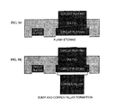
- FIGS. 5J to 5K are schematic views of a circuit board cross-section during steps from flash etching until bump and copper pillar formation according to a specific example of the method for fabricating a printed wiring board using the copper foil provided with a carrier according to the present invention.
- the copper foil provided with a carrier of the present invention has, in order, a carrier, an intermediate layer, and an ultrathin copper layer.
- Methods for using a copper foil provided with a carrier itself are well known to those skilled in the art.
- the surface of the ultrathin copper layer is pasted on an insulating substrate such as a paper substrate phenolic resin, a paper substrate epoxy resin, a synthetic fiber fabric substrate epoxy resin, a glass cloth-paper composite substrate epoxy resin, a glass cloth-glass non-woven composite substrate epoxy resin, and a glass cloth substrate epoxy resin, a polyester film and a polyimide film followed by heating and pressure-bonding; the carrier is then peeled off; the ultrathin copper layer adhered to the insulating substrate is etched in an intended conductive pattern; and eventually a laminate (a copper-clad laminate or the like), a printed wiring board, or the like can be fabricated.
- the carrier that can be used in the present invention is typically a metal foil or a resin film, and provided in the form of, for example, a copper foil, a copper alloy foil, a nickel foil, a nickel alloy foil, an iron foil, an iron alloy foil, a stainless steel foil, an aluminum foil, an aluminum alloy foil, an insulating resin film, a polyimide film, and an LCD film.
- the carrier that can be used in the present invention is typically provided in the form of a rolled copper foil or an electrolytic copper foil.
- an electrolytic copper foil is fabricated by electrolytic deposition of copper on a titanium or stainless steel drum from a copper sulfate bath, and a rolled copper foil is fabricated by repeating plastic working and heat treatment with a mill roll.
- the material for the copper foil in addition to high-purity copper, such as tough pitch copper (JIS H3100 alloy number C1100) and oxygen-free copper (JIS H3100 alloy number C1020 or JIS H3510 alloy number C1011), for example, copper alloys can also be used, such as Sn-containing copper, Ag-containing copper, a copper alloy to which Cr, Zr, Mg, or the like has been added, or a Colson copper alloy to which Ni, Si, and the like has been added.
- the carrier is preferably an electrolytic copper foil or a rolled copper foil because of a high conductivity, and further the carrier is more preferably an electrolytic copper foil because fabricating cost is low and it is easier to control the roughness of the carrier side surface. Note that, when the term “copper foil” is used singly herein, a copper alloy foil is also included therein.
- the thickness of the carrier that can be used in the present invention is not especially limited, the carrier may be appropriately adjusted to a suitable thickness in view its role as a carrier, such as, for example, 12 ⁇ m or more. However, since production costs increase if the carrier is too thick, generally it is preferred that the thickness is 35 ⁇ m or less. Therefore, the thickness of the carrier is typically 12 to 300 ⁇ m, more typically 12 to 150 ⁇ m, more typically 12 to 70 ⁇ m, and more typically 18 to 35 ⁇ m.
- the roughness of the surface of the carrier opposite to the ultrathin copper layer influences the peel strength between the ultrathin copper layer and the carrier in the laminate. It is believed that this is because, in forming an ultrathin copper layer above a carrier with an intermediate layer sandwiched therebetween, the roughness of the surface of the carrier opposite to the ultrathin copper layer larger than a predetermined value has some impact on the intermediate layer to increase the peel strength, for example.
- the roughness of the surface of the carrier opposite to the ultrathin copper layer larger than a predetermined value makes the current pathway on the surface of the carrier opposite to the ultrathin copper layer longer to make the surface less conductive, and as a result much current flows through the ultrathin copper layer side surface of the carrier, i.e., the intermediate layer and the ultrathin copper layer more easily than in conventional cases, which may be the cause of the influence.
- the peel strength is increased similarly. It is believed that this is because a current flowing in the direction opposite to that of a current in forming the ultrathin copper layer (reverse current) is generated in the intermediate layer in the step of roughening.
- the ten point average roughness Rz of the surface is controlled to be 6.0 ⁇ m or less. If the ten point average roughness Rz of the surface of the carrier opposite to the ultrathin copper layer is 6.0 ⁇ m or less, the peel strength of the ultrathin copper layer from the carrier is suppressed, which enables to peel the ultrathin copper layer form the carrier well.
- Rz is preferably 5.0 ⁇ m or less, more preferably 4.0 ⁇ m or less, and more preferably 3.5 ⁇ m or less.
- Rz is preferably 0.9 ⁇ m or more, preferably 1.0 ⁇ m or more, preferably 1.1 ⁇ m or more, more preferably 1.5 ⁇ m or more, and even more preferably 2.0 ⁇ m or more.
- the arithmetic average roughness Ra of the surface is controlled to be 1.0 ⁇ m or less. If the arithmetic average roughness Ra of the surface of the carrier opposite to the ultrathin copper layer is 1.0 ⁇ m or less, the peel strength of the ultrathin copper layer from the carrier is suppressed, which enables to peel the ultrathin copper layer form the carrier well.
- Ra is preferably 0.8 ⁇ m or less, more preferably 0.7 ⁇ m or less, and more preferably 0.6 ⁇ m or less.
- Ra is preferably 0.12 ⁇ m or more, preferably 0.15 ⁇ m or more, preferably 0.2 ⁇ m or more, more preferably 0.22 ⁇ m or more, and even more preferably 0.3 ⁇ m or more.
- the maximum cross-sectional height Rt in the roughness curve of the surface is controlled to be 7.0 ⁇ m or less. If the maximum cross-sectional height Rt of the surface of the carrier opposite to the ultrathin copper layer is 7.0 ⁇ m or less, the peel strength of the ultrathin copper layer from the carrier is suppressed, which enables to peel the ultrathin copper layer form the carrier well.
- Rt is preferably 6.0 ⁇ m or less, more preferably 5.0 ⁇ m or less, and more preferably 4.0 ⁇ m or less.
- Rt is preferably 1.1 ⁇ m or more, preferably 1.2 ⁇ m or more, preferably 1.3 ⁇ m or more, more preferably 1.5 ⁇ m or more, and even more preferably 2.0 ⁇ m or more.
- each of the above roughnesses of the surface of the carrier opposite to the ultrathin copper layer represents the roughness of the roughened layer surface
- a heat resistant layer, an anti-corrosion layer, a chromate-treated layer, and/or a silane coupling-treated layer described below are/is further formed on the roughened layer surface, the roughness of the surface of the outermost layer among them.
- each of the above roughnesses of the surface of the carrier opposite to the ultrathin copper layer represents the roughness of the surface of the outermost layer among them.
- the intermediate layer is provided above the carrier. Another layer may also be provided between the carrier and the intermediate layer.
- the intermediate layer used in the present invention is not especially limited, as long as the configuration of the copper foil provided with a carrier is such that the ultrathin copper layer does not easily peel from the carrier before the lamination step onto an insulating substrate, and such that the ultrathin copper layer can peel from the carrier after the lamination step onto the insulating substrate.
- the intermediate layer of the copper foil provided with a carrier according to the present invention may include one or two or more selected from the group consisting of Cr, Ni, Co, Fe, Mo, Ti, W, P, Cu, Al, and Zn, alloys thereof, hydrates thereof, oxides thereof, and organic substances. Further, a plurality of intermediate layers may be provided.
- the intermediate layer can be configured from the carrier side from a single metal layer formed from one element selected from the group of elements consisting of Cr, Ni, Co, Fe, Mo, Ti, W, P, Cu, Al, and Zn, or, configured by forming an alloy layer formed from one or two or more elements selected from the group of elements consisting of Cr, Ni, Co, Fe, Mo, Ti, W, P, Cu, Al, and Zn, and forming above that layer a layer formed from a hydrate or an oxide or an organic substance of one or two or more elements selected from the group of elements consisting of Cr, Ni, Co, Fe, Mo, Ti, W, P, Cu, Al, and Zn.
- the intermediate layer can be configured from the carrier side from a single metal layer formed from any one element of the group of elements of Cr, Ni, Co, Fe, Mo, Ti, W, P, Cu, Al, and Zn, or, configured by forming an alloy layer formed from one or more elements selected from the group of elements of Cr, Ni, Co, Fe, Mo, Ti, W, P, Cu, Al, and Zn, or an organic substance layer and subsequently forming a single metal layer formed from any one element of the group of elements of Cr, Ni, Co, Fe, Mo, Ti, W, P, Cu, Al, and Zn or an alloy layer formed from one or more elements selected from the group of elements of Cr, Ni, Co, Fe, Mo, Ti, W, P, Cu, Al, and Zn.
- a layer configuration which can be used as the intermediate layer may be used for the other layer.
- the intermediate layer can be configured by laminating a nickel layer, a nickel-phosphorus alloy layer, or a nickel-cobalt alloy layer, and a chromium-containing layer, in that order, on the carrier. Since the adhesive strength between nickel and copper is higher than the adhesive strength between chromium and copper, when the ultrathin copper layer is peeled, the peeling occurs at the interface between the ultrathin copper layer and the chromium. Further, the nickel in the intermediate layer can be expected to provide a barrier effect that prevents the diffusion of the copper component from the carrier into the ultrathin copper layer.
- the amount of nickel deposited in the intermediate layer is preferably 100 ⁇ g/dm 2 or more and 40,000 ⁇ g/dm 2 or less, more preferably 100 ⁇ g/dm 2 or more and 4,000 ⁇ g/dm 2 or less, more preferably 100 ⁇ g/dm 2 or more and 2,500 ⁇ g/dm 2 or less, and more preferably 100 ⁇ g/dm 2 or more and less than 1,000 ⁇ g/dm 2 .
- the amount of chromium deposited in the intermediate layer is preferably 5 ⁇ g/dm 2 or more and 500 ⁇ g/dm 2 or less, and more preferably 5 ⁇ g/dm 2 or more and 100 ⁇ g/dm 2 or less.
- the chromium-containing layer may be a chromium plating layer, a chromium alloy plating layer, or a chromate-treated layer.
- a chromate-treated layer refers to a layer treated with a solution containing chromic anhydride, chromic acid, dichromic acid, a chromate or a dichromate.
- the chromate-treated layer may contain an element such as cobalt, iron, nickel, molybdenum, zinc, tantalum, copper, aluminum, phosphorus, tungsten, tin, arsenic, and titanium (any form is available such as a metal, an alloy, an oxide, a nitride, and a sulfide).
- the chromate-treated layer examples include a chromate-treated layer which has been treated with chromic anhydride or an aqueous solution of potassium dichromate and a chromate-treated layer which has been treated with a treatment solution containing chromic anhydride or potassium dichromate and zinc.
- the intermediate layer of the copper foil provided with a carrier according to the present invention has a configuration in which a nickel layer or an alloy layer containing nickel, and an organic substance layer containing any of a nitrogen-containing organic compound, a sulfur-containing organic compound, and a carboxylic acid are laminated in order on the carrier, and the amount of nickel deposited in the intermediate layer may be 100 to 40,000 ⁇ m/dm 2 .
- an organic substance consisting of one or two or more selected from a nitrogen-containing organic compound, a sulfur-containing organic compound, and a carboxylic acid as the organic substance contained in the intermediate layer, for example.
- a nitrogen-containing organic compound, a sulfur-containing organic compound, and a carboxylic acid includes a nitrogen-containing organic compound having a substituent.
- 1,2,3-benzotriazole carboxybenzotriazole, N′,N′-bis(benzotriazolylmethyl)urea, 1H-1,2,4-triazole, 3-amino-1H-1,2,4-triazole, and the like, which are triazole compounds that have a substituent, as the nitrogen-containing organic compound.
- sulfur-containing organic compound it is preferred to use mercaptobenzothiazole, thiocyanuric acid, 2-benzimidazolethiol, and the like.
- carboxylic acid it is especially preferred to use a monocarboxylic acid, and among these, oleic acid, linoleic acid, linolenic acid, and the like.
- the above-described organic substance is preferably contained at a thickness of 8 nm or more and 80 nm or less, and more preferably 30 nm or more and 70 nm or less.
- the intermediate layer may contain multiple kinds of (one or more) the above-described organic substance.
- the thickness of the organic substance can be measured as follows.
- the exposed surface on the intermediate layer side of the ultrathin copper layer and the exposed surface on the intermediate layer side of the carrier are subjected to XPS measurement to make depth profiles.
- A depth at which the carbon concentration reaches 3 at % or less for the first time from the surface on the intermediate layer side of the ultrathin copper layer
- B depth at which the carbon concentration reaches 3 at % or less for the first time from the surface on the intermediate layer side of the carrier
- the sum of A and B can be regarded as the thickness (nm) of the organic substance in the intermediate layer.
- a method for using the organic substance contained in an intermediate layer will be described in the following with reference also to a method for forming an intermediate layer on a carrier foil.
- Formation of an intermediate layer on a carrier can be carried out by dissolving the above-described organic substance in a solvent and soaking a carrier in the solvent, or by using showering, a spraying method, a dropping method, an electrodeposition method, or the like for the surface on which an intermediate layer is to be formed, and it is unnecessary to employ a particularly limited method.
- the concentration of an organic agent in the solvent is preferably 0.01 g/L to 30 g/L
- the solution temperature is preferably in the range of 20 to 60° C. for all of the above-described organic substances.
- the concentration of the organic substance is not particularly limited, and whether the concentration is high or low does not matter essentially.
- the intermediate layer can be configured by laminating a nickel, and a molybdenum or cobalt or molybdenum-cobalt alloy, in that order, on a carrier. Since the adhesive strength between nickel and copper is higher than the adhesive strength between molybdenum or cobalt and copper, when the ultrathin copper layer is peeled off, the peeling occurs at the interface between the ultrathin copper layer and the molybdenum or cobalt or molybdenum-cobalt alloy. Further, the nickel in the intermediate layer is expected to provide a barrier effect that prevents the diffusion of the copper component from the carrier into the ultrathin copper layer.
- the amount of nickel deposited is 100 to 40,000 ⁇ g/dm 2 ; the amount of molybdenum deposited is 10 to 1,000 ⁇ g/dm 2 ; and the amount of cobalt deposited is 10 to 1,000 ⁇ g/dm 2 .
- the amount of Ni on the surface of the ultrathin copper layer after peeling the ultrathin copper layer from the copper foil provided with a carrier is controlled.
- the amount of Ni deposited in the intermediate layer is reduced and the intermediate layer contains a metal species (Co, Mo) which suppresses the diffusion of Ni into the ultrathin copper layer side.
- the amount of nickel deposited is preferably 100 to 40,000 ⁇ g/dm 2 , preferably 200 to 20,000 ⁇ g/dm 2 , more preferably 300 to 15,000 ⁇ g/dm 2 , and more preferably 300 to 10,000 ⁇ g/dm 2 .
- the amount of molybdenum deposited is preferably 10 to 1,000 ⁇ g/dm 2 and the amount of molybdenum deposited is preferably 20 to 600 ⁇ g/dm 2 , and more preferably 30 to 400 ⁇ g/dm 2 .
- the amount of cobalt deposited is preferably 10 to 1,000 ⁇ g/dm 2 and the amount of cobalt deposited is preferably 20 to 600 ⁇ g/dm 2 , and more preferably 30 to 400 ⁇ g/dm 2 .
- the density of the molybdenum or cobalt or molybdenum-cobalt alloy layer tends to be increased when the current density is lowered and the conveying speed of the carrier is lowered in a plating treatment to provide the molybdenum or cobalt or molybdenum-cobalt alloy layer. If the density of the layer containing molybdenum and/or cobalt is high, the nickel in the nickel layer is less likely to diffuse, which enables to control the amount of Ni on the ultrathin copper layer surface after peeling.
- the intermediate layer can be provided by performing for a carrier a wet plating such as an electroplating, an electroless plating, and an immersion plating, or a dry plating such as a sputtering, a CVD, and a PVD.
- a wet plating such as an electroplating, an electroless plating, and an immersion plating
- a dry plating such as a sputtering, a CVD, and a PVD.
- a pretreatment such as an activation treatment for subjecting the carrier to a wet plating before formation of the intermediate layer.
- the above-described pretreatment which can be used may be any treatment as long as it enables to perform a wet plating for a resin film, and known treatments can be used.
- An ultrathin copper layer is provided above the intermediate layer.
- strike plating may be carried out with a copper-phosphorous alloy to reduce the number of pinholes in the ultrathin copper layer.
- a copper pyrophosphate solution and the like may be used for the strike plating.
- An ultrathin copper layer is provided above the intermediate layer.
- another layer may also be provided between the intermediate layer and the ultrathin copper layer.
- the ultrathin copper layer can be formed through an electroplating utilizing an electrolytic bath of copper sulfate, copper pyrophosphate, copper sulfamate, copper cyanide, or the like, and a copper sulfate bath is preferred because it is used for a common electrolytic copper foil and enables to form a copper foil at a high current density.
- the thickness of the ultrathin copper layer is not particularly limited, the ultrathin copper layer is usually thinner than the carrier, and may be, for example, 12 ⁇ m or less.
- the thickness of the ultrathin copper layer is typically 0.05 to 12 ⁇ m, more typically 0.1 to 12 ⁇ m, 0.5 to 12 ⁇ m, more typically 1.5 to 5 ⁇ m, and more typically 2 to 5 ⁇ m. Further, a layer having a configuration which can be used as the intermediate layer may be used as the other layer.
- a roughened layer may be provided on the surface of the carrier opposite to the ultrathin copper layer side by performing a roughening treatment in order to make the close adhesion properties to a resin substrate good, for example.
- no roughened layer may be formed on the surface of the carrier opposite to the ultrathin copper layer side.
- no roughened layer is formed on the surface of the carrier opposite to the ultrathin copper layer side, there is an advantage that it is easier to control the peel strength between the carrier and the ultrathin copper layer.
- a roughened layer may be provided on the surface of the ultrathin copper layer by performing a roughening treatment in order to make the close adhesion properties to an insulating substrate good, for example.
- “surface of the carrier opposite to the ultrathin copper layer” on which a roughened layer, a heat resistant layer, an anti-corrosion layer, a chromate-treated layer, a silane coupling-treated layer, or the like is to be formed or on which no roughened layer is formed is not particularly limited as long as the surface is located opposite to the ultrathin copper layer across the carrier.
- the surface of the carrier opposite to the ultrathin copper layer may be the surface of the carrier itself, or in the case that a surface-treated layer is formed on the carrier opposite to the ultrathin copper layer, may be the surface of any of layers in the surface-treated layer (including the surface of the outermost layer).
- the roughening treatment performed for the carrier or the ultrathin copper layer can be carried out by forming roughened particles with copper or a copper alloy, for example.
- the roughening treatment may be a fine treatment.
- the roughened layer may be a layer consisting of a simple substance selected from the group consisting of copper, nickel, cobalt, phosphorous, tungsten, arsenic, molybdenum, chromium, and zinc or an alloy containing one or more thereof, or the like.
- a roughening treatment can be carried out in which secondary particles or tertiary particles are further provided using a simple substance of nickel, cobalt, copper, or zinc, an alloy thereof, or the like.
- the roughened layer may be formed using a sulfuric acid-copper sulfate electrolytic bath containing one or more selected from the group consisting of a sulfuric acid alkyl ester salt, tungsten, and arsenic.
- the roughening treatment can be performed using the following electrolytic bath under the following conditions.
- cover plating may be performed after the roughening treatment in order to prevent the roughened particle from being peeled out.
- a heat resistant layer or an anti-corrosion layer may be formed with a simple substance of nickel, cobalt, copper, or zinc, an alloy thereof, or the like, and further for the surface a treatment such as a chromate treatment and a silane coupling treatment may be performed.
- a heat resistant layer or an anti-corrosion layer is formed with a simple substance of nickel, cobalt, copper, or zinc, an alloy thereof, or the like without performing a roughening treatment, further for the surface a treatment such as a chromate treatment and a silane coupling treatment may be performed.
- one or more layers selected from the group consisting of a heat resistant layer, an anti-corrosion layer, a chromate-treated layer, and a silane coupling-treated layer may be formed on the surface of the roughened layer, or one or more layers selected from the group consisting of a heat resistant layer, an anti-corrosion layer, a chromate-treated layer, and a silane coupling-treated layer may be formed on the surface of the carrier or the ultrathin copper layer.
- the above-described heat resistant layer, anti-corrosion layer, chromate-treated layer, and silane coupling-treated layer may be each formed in a plurality of layers (e.g., two or more layers, three or more layers, or the like). These surface treatments have little influence on the surface roughness of the carrier and the ultrathin copper layer.
- the roughening treatment can be carried out by forming roughened particles with copper or a copper alloy, for example.
- fine particles constitute the roughened layer from the perspective of formation of a fine pitch.
- the electroplating conditions in forming roughened particles a high current density, a low copper concentration in the plating solution, or a large quantity of coulomb tends to make the particles fine.
- a laminate e.g., a copper-clad laminate
- a laminate can be produced by pasting a copper foil provided with a carrier on an insulating resin sheet from the ultrathin copper layer side followed by heating and pressure-bonding, and then peeling off the carrier. Further thereafter, the ultrathin copper layer portion can be etched to form a copper circuit for a printed wiring board.
- the insulating resin sheet to be used here is not especially limited as long as the insulating resin sheet has properties that allow to it to be applied in a printed wiring board.
- Examples that can be used include, for a rigid PWB, a paper substrate phenolic resin, a paper substrate epoxy resin, a synthetic fiber fabric substrate epoxy resin, a glass cloth-paper composite substrate epoxy resin, a glass cloth-glass non-woven composite substrate epoxy resin, and a glass cloth substrate epoxy resin, and for an FPC, a polyester film and a polyimide film.
- the printed wiring board or the laminate produced in this way can be mounted on various electronic components for which high-density implementation of mounted components is required.
- a “printed wiring board” includes a printed wiring board with components equipped thereon and a printed circuit board and a printed substrate.
- an electronic device can be fabricated using such a printed wiring board.
- a “copper circuit” includes a copper wiring.
- the copper foil provided with a carrier may be provided with a roughened layer above the ultrathin copper layer, and may be provided with one or more layers selected from the group consisting of a heat resistant layer, an anti-corrosion layer, a chromate-treated layer, and a silane coupling-treated layer above the roughened layer.
- the copper foil provided with a carrier may be provided with a roughened layer above the ultrathin copper layer, and may be provided with a heat resistant layer or anti-corrosion layer above the roughened layer, and may be provided with a chromate-treated layer above the heat resistant layer or anti-corrosion layer, and may be provided with a silane coupling-treated layer above the chromate-treated layer.
- the copper foil provided with a carrier may be provided with a resin layer above the ultrathin copper layer, or above the roughened layer, or above the heat resistant layer or anti-corrosion layer, or a chromate-treated layer, or a silane coupling-treated layer.
- the above-described resin layer may be an adhesive, and may also be an insulating resin layer in a semi-cured state (B stage state) for adhesion.
- This semi-cured state (B stage state) includes states in which there is no stickiness feeling even if the surface is touched with a finger, the insulating resin layer can be stacked and stored, and a curing reaction occurs when further subjected to a heating treatment.
- the above-described resin layer may include a thermosetting resin, or may be a thermoplastic resin.
- the above-described resin layer may include a thermoplastic resin.
- This resin layer may include known resins, resin curing agents, compounds, curing accelerators, dielectrics, reaction catalysts, cross-linking agents, polymers, prepregs, skeletal materials, and the like.
- the resin layer may be formed using the substances (resins, resin curing agents, compounds, curing accelerators, dielectrics, reaction catalysts, cross-linking agents, polymers, prepregs, skeletal materials, and the like) and/or resin layer formation method and formation apparatus described in International Publication No. WO 2008/004399, International Publication No.
- WO 2006/134868 Japanese Patent No. 5046927, Japanese Patent Laid-Open No. 2009-173017, International Publication No. WO 2007/105635, Japanese Patent No. 5180815, International Publication No. WO 2008/114858, International Publication No. WO 2009/008471, Japanese Patent Laid-Open No. 2011-14727, International Publication No. WO 2009/001850, International Publication No. WO 2009/145179, International Publication No. WO 2011/068157, Japanese Patent Laid-Open No. 2013-19056.
- the type of the above-described resin layer is not especially limited.
- preferred resins can include one or more selected from the group consisting of epoxy resins, polyimide resins, polyfunctional cyanate compounds, maleimide compounds, polymaleimide compounds, maleimide resins, aromatic maleimide resins, polyvinyl acetal resins, urethane resins, polyether sulfone (also called polyether sulphone), polyether sulfone (also called polyether sulphone) resins, aromatic polyamide resins, aromatic polyamide resin polymers, rubber resins, polyamines, aromatic polyamines, polyamide-imide resins, rubber-modified epoxy resins, phenoxy resins, carboxyl group-modified acrylonitrile-butadiene resins, polyphenylene oxide, bismaleimide triazine resins, thermosetting polyphenylene oxide resins, cyanate ester resins, carboxylic acid anhydrides, polybasic carboxylic acid anhydrides, linear polymers having
- epoxy resin can be used without any particular problem as long as it has two or more epoxy groups in the molecule and can be used in electrical/electronic material applications.
- an epoxy resin epoxied using a compound having two or more glycidyl groups in the molecule is preferred.
- epoxy resins that can be used include one or a mixture of two or more selected from the group consisting of bisphenol A type epoxy resins, bisphenol F type epoxy resins, bisphenol S type epoxy resins, bisphenol AD type epoxy resins, novolak type epoxy resins, cresol novolak type epoxy resins, alicyclic epoxy resins, brominated epoxy resins, phenol novolak type epoxy resins, naphthalene type epoxy resins, brominated bisphenol A type epoxy resins, ortho-cresol novolak type epoxy resins, rubber-modified bisphenol A type epoxy resins, glycidyl amine compounds such as glycidyl amine type epoxy resins, triglycidyl isocyanurate, and N,N-diglycidyl aniline, glycidyl ester compounds such as diglycidyl tetrahydrophthalate, phosphorus-containing epoxy resins, biphenyl type epoxy resins, biphenyl novolak type epoxy resins, tris
- a known phosphorus-containing epoxy resin can be used for the above-described phosphorus-containing epoxy resin. Further, it is preferred that the above-described phosphorus-containing epoxy resin is an epoxy resin obtained as a derivative from, for example, 9,10-dihydro-9-oxa-10-phosphaphenanthrene-10-oxide that includes two or more epoxy groups in the molecule.
- the resin layer may include a dielectric filler.
- a dielectric dielectric filler
- the dielectric is used for an application of forming a capacitor layer and thereby enables to increase the capacitance of a capacitor circuit.
- this dielectric (dielectric filler) a dielectric powder of a complex oxide having a perovskite structure such as BaTiO 3 , SrTiO 3 , Pb(Zr—Ti)O 3 (commonly called PZT), PbLaTiO 3 .PbLaZrO (commonly called PLZT), and SrBi 2 Ta 2 O 9 (commonly called SBT).
- the resin and/or resin composition and/or compound included in the above-described resin layer is obtained in a B stage state by, for example, dissolving in a solvent such as methyl ethyl ketone (MEK), cyclopentanone, dimethylformamide, dimethylacetamide, N-methylpyrrolidone, toluene, methanol, ethanol, propylene glycol monomethyl ether, dimethylformamide, dimethylacetamide, cyclohexanone, ethyl cellosolve, N-methyl-2-pyrrolidone, N,N-dimethylacetamide, N,N-dimethylformamide to produce a resin solution (resin varnish), coating the resin solution on the surface on the ultrathin copper layer side of the copper foil provided with a carrier by a roll coater method, for example, and then heating and drying as necessary to remove the solvent.
- a solvent such as methyl ethyl ketone (MEK), cyclopentanone, di
- the drying can be carried out using, for example, a hot air drying furnace, at a drying temperature of 100 to 250° C., and preferably 130 to 200° C.
- the composition of the above-described resin layer may be dissolved using a solvent to obtain the resin solution having a resin solid content of 3% by weight to 70% by weight, preferably 3% by weight to 60% by weight, preferably 10% by weight to 40% by weight, and more preferably 25% by weight to 40% by weight.
- a solvent having a boiling point in the range of 50° C. to 200° C.
- the above-described resin layer is a semi-cured resin film having a resin flow when measured based on MIL-P-13949G in the MIL standards in the range of 5% to 35%.
- the resin flow is a value obtained by, based on MIL-P-13949G in the MIL standards, sampling four 10-cm square specimens from a surface-treated copper foil provided with a resin having a resin thickness of pasting the four specimens in a stacked state (as a laminate) under conditions of a pressing temperature of 171° C., a pressing pressure of 14 kgf/cm 2 , and a pressing time of 10 minutes, and calculating the resin flow weight at that point from the measured results based on the following formula.
- Resin ⁇ ⁇ flow ⁇ ⁇ ( % ) Resin ⁇ ⁇ flow ⁇ ⁇ weight ( Laminate ⁇ ⁇ weight ) - ( Copper ⁇ ⁇ foil ⁇ ⁇ weight ) ⁇ 100
- the surface-treated copper foil (surface-treated copper foil provided with a resin) including the above-described resin layer is used in a mode for forming a predetermined wiring pattern from the surface on the opposite side to the side subjected to the roughening treatment of the surface-treated copper foil by stacking the resin layer on the base material, then heating and pressure-bonding the whole stack to thermally cure the resin layer, and if the surface-treated copper foil is an ultrathin copper layer of a copper foil provided with a carrier, then peeling the carrier to expose the ultrathin copper layer to the surface (naturally the exposed portion is the surface on the intermediate layer side of the ultrathin copper layer).
- this surface-treated copper foil provided with a resin is used, the number of sheets of prepreg material used when fabricating a multilayer printed wiring board can be reduced. Moreover, the thickness of the resin layer can be set to a thickness that ensures interlayer insulation, and a copper-clad laminate can be fabricated even without using a prepreg material at all. Further, at this point, the smoothness of the surface can be further improved by applying an insulating resin as an undercoat on the surface of the base material.
- the thickness of the multilayer printed wiring board to be fabricated is thinner by the thickness amount of the prepreg material, so that a very thin multilayer printed wiring board in which the thickness of one layer is 100 ⁇ m or less can be fabricated.
- the thickness of this resin layer is preferably 0.1 to 500 ⁇ m more preferably 0.1 to 300 ⁇ m, more preferably 0.1 to 200 ⁇ m, and more preferably 0.1 to 120 ⁇ m.
- the thickness of the resin layer is thinner than 0.1 ⁇ m the adhesive strength can deteriorate, and it can become difficult to ensure interlayer insulation between an inner layer material and the circuit when this copper foil provided with a carrier provided with a resin is laminated on a base material including an inner layer material without arranging a prepreg material therebetween.
- the resin layer thickness is thicker than 120 ⁇ m, it can be difficult to form a resin layer with a target thickness in one coating step, so that extra material costs and steps are required, which is economically disadvantageous.
- the thickness of the above-described resin layer is 0.1 ⁇ m to 5 ⁇ m, more preferably 0.5 ⁇ m to 5 ⁇ m, and more preferably 1 ⁇ m to 5 ⁇ m, because the thickness of the multilayer printed wiring board is smaller.
- the thickness of the resin layer is 0.1 ⁇ m to 5 ⁇ m
- the above-described thickness of a resin layer is the average value of thicknesses measured by cross-sectional observation at arbitrary 10 points.
- this copper foil provided with a carrier provided with a resin
- An embodiment of the method for fabricating a printed wiring board according to the present invention includes forming a copper-clad laminate by carrying out a step of preparing the copper foil provided with a carrier according to the present invention and an insulating substrate, a step of laminating the copper foil provided with a carrier and the insulating substrate, and a step of, after the copper foil provided with a carrier and the insulating substrate have been laminated in such a manner that the ultrathin copper layer side of the copper foil faces the insulating substrate, peeling the carrier of the copper foil provided with a carrier, and then forming a circuit by any of a semi-additive method, a modified semi-additive method, a partly additive method, and a subtractive method.
- the insulating substrate can also be formed between the inner layer circuits.
- semi-additive method refers to a method for forming a pattern by performing thin electroless plating on an insulating substrate or a copper foil seed layer, and then forming a conductive pattern using electrolytic plating and etching.
- an embodiment of a method for fabricating a printed wiring board according to the present invention using a semi-additive method includes
- modified semi-additive method refers to a method for forming a circuit on an insulating layer by laminating a metal foil on an insulating layer, protecting a non-circuit formed portion with a plating resist, performing copper thickening of a circuit formed portion by electrolytic plating, then removing the resist, and removing the metal foil at portions other than the circuit formed portion by (flash) etching.
- an embodiment of a method for fabricating a printed wiring board according to the present invention using a modified semi-additive method includes
- partly additive method refers to a method for fabricating a printed wiring board by providing a catalyst core on a substrate that is provided with a conductive layer and in which holes for through-holes and via holes have optionally been opened, forming a conductive circuit by etching, optionally providing a solder resist or a plating resist, and then performing thickening on the conductive circuit by an electroless plating treatment on the through-holes, via holes, and the like.
- an embodiment of a method for fabricating a printed wiring board according to the present invention using a partly additive method includes
- subtractive method refers to a method for forming a conductive pattern by selectively removing an unnecessary portion of copper foil on a copper-clad laminate by etching and the like.
- an embodiment of a method for fabricating a printed wiring board according to the present invention using a subtractive method includes
- the step of providing a through-hole and/or a blind via and the subsequent desmearing step do not have to be carried out.
- a copper foil provided with a carrier (first layer) having an ultrathin copper layer on which a roughened layer has been formed on the surface is prepared.
- a resist is coated on the roughened layer of the ultrathin copper layer, exposure and development is carried out, and the resist is etched into a predetermined shape.
- a plating for a circuit is formed, and then the circuit plating is formed in a predetermined shape by removing the resist.
- a resin layer is laminated by providing an embedded resin on the ultrathin copper layer so as to cover the circuit plating (so as to bury the circuit plating), and then a separate copper foil provided with a carrier (second layer) is adhered from the ultrathin copper layer side.
- the carrier is peeled from the second layer of the copper foil provided with a carrier.
- laser hole opening is performed on a predetermined position of the resin layer, and the circuit plating is exposed to form a blind via.
- FIG. 4H a circuit plating is formed as illustrated in the above-described FIGS. 2B and 2C on the via fill.
- the carrier is peeled from the first layer of the copper foil provided with a carrier.
- the ultrathin copper layer on both surfaces is removed by flash etching to expose the surface of the circuit plating in the resin layer.
- a bump is formed on the circuit plating in the resin layer, and a copper pillar is formed on that solder. In this manner, a printed wiring board using the copper foil provided with a carrier according to the present invention is produced.
- the copper foil provided with a carrier can be used, a conventional copper foil provided with a carrier may be used, or a normal copper foil may be used.
- a circuit may be formed in one layer or a plurality of layers on the circuit of the second layer illustrated in FIG. 4H . These circuits can be formed by any of a semi-additive method, a subtractive method, a partly additive method, and a modified semi-additive method.
- the copper foil provided with a carrier used for the first layer may have a substrate on the carrier side surface of the copper foil provided with a carrier.
- the copper foil provided with a carrier used for the first layer is supported, so that wrinkles are less likely to form. Consequently, there is the advantage that productivity is improved.
- any substrate may be used for this substrate, as long as the substrate has an effect of supporting the above-described copper foil provided with a carrier used for the first layer.
- the carrier, the prepreg, and the resin layer described in the specification of the present application or a known carrier, prepreg, resin layer, metal sheet, metal foil, sheet of an inorganic compound, foil of an inorganic compound, sheet of an organic compound, or foil of an organic compound can be used as the above-described substrate.
- the timing to form a substrate on the carrier side surface is not particularly limited, it is necessary to form a substrate before peeling off the carrier.
- it is preferred to form a substrate before a step of forming a resin layer on the ultrathin copper layer side surface of the copper foil provided with a carrier and it is more preferred to form a substrate before a step of forming a circuit on the ultrathin copper layer side surface of the copper foil provided with a carrier.
- the above-described ⁇ E*ab is preferably 50 or more, more preferably 55 or more, and even more preferably 60 or more. If the color difference ⁇ E*ab based on JIS Z8730 of the ultrathin copper layer surface is 45 or more, for example, when forming a circuit on the ultrathin copper layer surface of the copper foil provided with a carrier, the contrast between the ultrathin copper layer and the circuit becomes very clear, so that as a result visibility is good and the positioning of the circuit can be carried out precisely.
- color difference of the ultrathin copper layer surface refers to the color difference of the surface of the ultrathin copper layer, or, in the case that various surface-treated layers have been provided, such as a roughened layer, a heat resistant layer, an anti-corrosion layer, a chromate-treated layer, and a silane coupling-treated layer, the color difference of the surface of that surface-treated layer (outermost surface).
- the above-described color difference ⁇ E*ab is represented by the following equation.
- the color differences ⁇ L, ⁇ a, and ⁇ b in the following equation are each measured with a colorimeter.
- These color differences are a general index represented using an L*a*b* color system based on JIS Z8730 (2009) tinted with black/white/red/green/yellow/blue, in which ⁇ L is represented as white/black, ⁇ a as red/green, and ⁇ b as yellow/blue.
- the color differences ( ⁇ L, ⁇ a, ⁇ b) can be measured using the colorimeter MiniScan XE Plus manufactured by HunterLab.
- the color differences ⁇ L, ⁇ a, ⁇ b are each a color difference based on JIS Z8730 (2009) of the ultrathin copper layer surface when the reference color is defined as the object color of the above-described white board
- ⁇ L is the difference of CIE luminosity L* between two object colors in an L*a*b* color system defined in JIS Z8729 (2004)
- ⁇ a and ⁇ b are the difference of a color coordinate a* or b*, respectively, between two object colors in an L*a*b* color system defined in JIS Z8729 (2004).
- ⁇ E*ab ⁇ square root over ( ⁇ L 2 + ⁇ a 2 + ⁇ b 2 ) ⁇
- the above-described color difference can be adjusted by increasing the current density during ultrathin copper layer formation, reducing the copper concentration in the plating solution, and increasing the linear flow rate of the plating solution.
- the above-described color difference can also be adjusted by providing a roughened layer by performing a roughening treatment on the surface of the ultrathin copper layer.
- a roughened layer is provided, the adjustment can be carried out using an electrolyte including copper and one or more elements selected from the group consisting of nickel, cobalt, tungsten, and molybdenum, increasing the current density higher than for a conventionally (e.g., to 40 to 60 A/dm 2 ), and shortening the treatment time (e.g., to 0.1 to 1.3 seconds).
- the adjustment can be carried out using a plating bath that contains Ni in a concentration twice or more that of other elements, and performing Ni alloy plating (e.g., Ni—W alloy plating, Ni—Co—P alloy plating, and Ni—Zn alloy plating) on the surface of the ultrathin copper layer, or a heat resistant layer, or an anti-corrosion layer, or a chromate-treated layer, or a silane coupling-treated layer by setting a lower current density than conventionally (e.g., 0.1 to 1.3 A/dm 2 ) and a longer treatment time (e.g., 20 seconds to 40 seconds).
- Ni alloy plating e.g., Ni—W alloy plating, Ni—Co—P alloy plating, and Ni—Zn alloy plating
- a known resin and prepreg can be used for the buried resin.
- a BT (bismaleimide triazine) resin a glass cloth prepreg impregnated with a BT resin, an ABF film or ABF manufactured by Ajinomoto Fine-Techno Co., Inc.
- the resin layer and/or resin and/or prepreg described in the present specification can be used for the above-described buried resin.
- the method for fabricating a printed wiring board according to the present invention may be a method for fabricating a printed wiring board including: a step of laminating the ultrathin copper layer side surface or the carrier side surface of the copper foil provided with a carrier according to the present invention and a resin substrate; a step of providing two layers of a resin layer and a circuit at least one time on the surface of the copper foil provided with a carrier opposite to the ultrathin copper layer side surface or the carrier side surface with the resin substrate laminated thereon; and a step of, after the two layers of the resin layer and the circuit have been formed, peeling the carrier or the ultrathin copper layer from the copper foil provided with a carrier (coreless method).
- the ultrathin copper layer side surface or the carrier side surface of the copper foil provided with a carrier according to the present invention and a resin substrate are laminated to fabricate a laminate.
- a resin layer is formed on the surface of the copper foil provided with a carrier opposite to the ultrathin copper layer side surface or the carrier side surface with the resin substrate laminated thereon.
- a separate copper foil provided with a carrier may be laminated from the carrier side or the ultrathin copper layer side on the resin layer formed on the carrier side surface or the ultrathin copper layer side surface.
- a laminate having a configuration in which a copper foil provided with a carrier is laminated on both surfaces of the resin substrate, which is positioned at the center, in an order of a carrier/an intermediate layer/an ultrathin copper layer or an ultrathin copper layer/an intermediate layer/a carrier, or a laminate having a configuration in which “a carrier/an intermediate layer/an ultrathin copper layer/a resin substrate/an ultrathin copper layer/an intermediate layer/a carrier” are laminated in this order may be used for the above-described method for fabricating a printed wiring board (coreless method).
- a separate resin layer may be further provided to form a circuit by further providing a copper layer or metal layer and thereafter processing the copper layer or metal layer.
- a separate resin layer may be further provided on the circuit so as to bury the circuit. Further, such formation of a circuit and a resin layer may be carried out one or more times (build-up method).
- laminate B a coreless substrate can be produced by peeling the ultrathin copper layer or the carrier of each copper foil provided with a carrier from the carrier or the ultrathin copper layer.
- two copper foils provided with a carrier can be used to produce a laminate having a configuration of an ultrathin copper layer/an intermediate layer/a carrier/a carrier/an intermediate layer/an ultrathin copper layer, a laminate having a configuration of a carrier/an intermediate layer/an ultrathin copper layer/an ultrathin copper layer/an intermediate layer/a carrier, or a laminate having a configuration of a carrier/an intermediate layer/an ultrathin copper layer/a carrier/an intermediate layer/an ultrathin copper layer as described below to use the laminate as the center.
- a coreless substrate can be produced by providing two layers of a resin layer and a circuit one or more times on surfaces of the ultrathin copper layers or the carriers on both sides of these laminates (hereinafter, also referred to as laminate A), and, after the two layers of the resin layer and the circuit have been provided, peeling the ultrathin copper layer or the carrier of each copper foil provided with a carrier from the carrier or the ultrathin copper layer.
- laminate A may have another layer on the surface of the ultrathin copper layer, on the surface of the carrier, between the carriers, between the ultrathin copper layers, or between the ultrathin copper layer and the carrier.
- the other layer may be a resin layer or a resin substrate.
- an ultrathin copper layer, a carrier, or a laminate has another layer on the ultrathin copper layer surface, the carrier surface, or the laminate surface
- “surface of an ultrathin copper layer,” “ultrathin copper layer side surface,” “ultrathin copper layer surface,” “surface of a carrier,” “carrier side surface,” “carrier surface,” “surface of a laminate,” and “laminate surface” are a concept also including the surface (outermost surface) of the another layer.
- the laminate preferably has a configuration of an ultrathin copper layer/an intermediate layer/a carrier/a carrier/an intermediate layer/an ultrathin copper layer.
- the ultrathin copper layer is disposed on the coreless substrate side, which facilitates formation of a circuit on the coreless substrate using a modified semi-additive method.
- the reason is that, since the thickness of the ultrathin copper layer is small, it is easy to remove the ultrathin copper layer, which facilitates formation of a circuit on the coreless substrate using a semi-additive method after removing the ultrathin copper layer.
- laminate which is not particularly stated as “laminate A” or “laminate B” indicates a laminate including at least a laminate A and a laminate B.
- a resin which can be used for the resin layer can be used. Further, in the above-described method for fabricating a coreless substrate, when the copper foil provided with a carrier or the laminate is viewed in a plane, at least a part of the periphery of a laminated part of the copper foil provided with a carrier or the laminate (a laminated part of a carrier and an ultrathin copper layer, or a laminated part of one copper foil provided with a carrier and another copper foil provided with a carrier) may be covered with a resin or a prepreg.
- a laminate (laminate A) formed by using the above-described method for fabricating a coreless substrate may have a configuration in which a pair of copper foils provided with a carrier are contacted with each other in a separable manner. Furthermore, when the copper foil provided with a carrier is viewed in a plane, all of the periphery of a laminated part of the copper foil provided with a carrier or the laminate (a laminated part of a carrier and an ultrathin copper layer, or a laminated part of one copper foil provided with a carrier and another copper foil provided with a carrier) may be covered with a resin or a prepreg.
- the laminated part of the copper foil provided with a carrier or the laminate is covered with a resin or a prepreg, and it can be prevented for another member to touch from the lateral direction of this part, that is, the transverse direction against the lamination direction, and as a result, the peeling of the carrier and the ultrathin copper layer or copper foils provided with a carrier can be less likely to occur in handling.
- the above-described permeation of a chemical solution into the interface of this laminated part in a chemical solution treatment step can be prevented, and the corrosion and erosion of the copper foil provided with a carrier can be prevented.
- the laminated part of the copper foil provided with a carrier or the laminate (the laminated part of the carrier and the ultrathin copper layer, or the laminated part of one copper foil provided with a carrier and another copper foil provided with a carrier) covered with a resin or a prepreg needs to be removed by cutting or the like.
- the copper foil provided with a carrier according to the present invention may be laminated from the carrier side or the ultrathin copper layer side on the carrier side or the ultrathin copper layer side of another copper foil provided with a carrier according to the present invention to constitute a laminate.
- the laminate may be a laminate obtained by directly laminating as necessary via an adhesive the carrier side surface or the ultrathin copper layer side surface of the one copper foil provided with a carrier and the carrier side surface or the ultrathin copper layer side surface of the another copper foil provided with a carrier.
- the carrier or the ultrathin copper layer of the one copper foil provided with a carrier and the carrier or the ultrathin copper layer of the another copper foil provided with a carrier may be bonded together.
- the “bonding” includes a mode in which they are bonded together via the surface-treated layer.
- a part or all of the edge face of the laminate may be covered with a resin.
- Lamination of carriers can be carried out by simply stacking or, for example, by using the following methods.
- a laminate having a configuration in which one carrier and the other carrier are laminated and contacted with each other in a separable manner can be fabricated. If one carrier and the other carrier are laminated in a state that one carrier and the other carrier are weakly bonded together, one carrier and the other carrier are separable from each other even without removing the bonding part of one carrier and the other carrier. On the other hand, if one carrier and the other carrier are strongly bonded together, one carrier and the other carrier can be separated from each other by removing the part to which one carrier and the other carrier bonds by cutting, chemical polishing (e.g., etching), mechanical polishing, or the like.
- chemical polishing e.g., etching
- a printed wiring board can be produced by performing a step of providing two layers of a resin layer and a circuit at least one time on the laminate configured in this way, and a step of, after the two layers of the resin layer and the circuit have been formed at least one time, peeling the ultrathin copper layer or the carrier from the copper foil provided with a carrier of the laminate.
- two layers of a resin layer and a circuit may be provided on the surface of one side or both sides of the laminate.
- the resin substrate, resin layer, resin, or prepreg to be used for the above-described laminate may be the resin layer described herein, and may include resins used for the resin layer described herein, resin curing agents, compounds, curing accelerators, dielectrics, reaction catalysts, cross-linking agents, polymers, prepregs, skeletal materials, and the like.
- the copper foil provided with a carrier may be smaller than the resin substrate, resin layer, resin, or prepreg when being viewed in a plane.
- the surface roughness of a rolled copper foil can be controlled by controlling the surface roughness of a mill roll used in rolling.
- the surface roughness of a rolled copper foil can be increased by increasing the surface roughness of a mill roll used in rolling.
- the surface roughness of the shiny surface (glossy surface) of an electrolytic copper foil can be controlled by controlling the surface roughness of an electrolytic drum used in fabricating an electrolytic copper foil.
- the surface roughness of the shiny surface (glossy surface) of an electrolytic copper foil can be increased by increasing the surface roughness of an electrolytic drum.
- the surface roughness of the mat surface (deposition surface) of an electrolytic copper foil can be controlled by controlling the copper concentration of an electrolyte, the current density, and the electrolyte temperature in fabricating an electrolytic copper foil.
- the surface roughness of the mat surface (deposition surface) of an electrolytic copper foil can be increased by decreasing the copper concentration of an electrolyte, increasing the current density, and lowering the electrolyte temperature in fabricating an electrolytic copper foil.
- the surface roughness of the mat surface (deposition surface) of an electrolytic copper foil can be decreased by increasing the copper concentration of an electrolyte, decreasing the current density, and raising the electrolyte temperature in fabricating an electrolytic copper foil.
- an electrolyte concentration of an electrolyte it is recommended to set the copper concentration of an electrolyte to 50 to 130 g/L, the current density to 50 to 120 A/dm 2 , and the electrolyte temperature to 40 to 90° C., for example.
- an aqueous solution of sulfuric acid and copper sulfate was used for the electrolyte in fabricating an electrolytic copper foil.
- Known gloss agents can be used for the gloss agent.
- Example 6 Cl ⁇ : 20 to 50 ppm by mass, polyethylene glycol: 10 to 100 ppm by mass, bis(3-sulfopropyl)disulfide: 10 to 30 ppm by mass, and thiourea: 10 to 50 ppm by mass were added as the gloss agent.
- Example 23 Cl ⁇ : 30 to 80 ppm by mass, bis(3-sulfopropyl)disulfide: 10 to 50 ppm by mass, and thiourea: 10 to 50 ppm by mass were added as the gloss agent.
- An amine compound represented by the following structural formula: 10 to 50 ppm was added:
- R 1 and R 2 are selected from the group consisting of a hydroxyalkyl group, an ether group, an aromatic group, an aromatic-substituted alkyl group, an unsaturated hydrocarbon group, and an alkyl group.
- An intermediate layer was formed on a carrier as described in the column “Intermediate Layer” in Table.
- the treatment conditions are shown below. Note that, for example, “Ni/organic substance” means that a nickel plating treatment was performed followed by an organic substance treatment.
- the glossy surface (shiny surface) of the above electrolytic copper foil or the rolled copper foil was provided with an intermediate layer with a roll-to-roll continuous plating line under the following conditions.
- Ni Ni Treatment (Ni Plating)
- Solution composition nickel sulfate concentration of 200 to 300 g/L, trisodium citrate concentration of 2 to 10 g/L
- a treatment solution used in electrolysis, a surface treatment, plating, or the like employed in the present invention is water unless otherwise noted.
- a Cr layer in an amount to be deposited of 10 ⁇ g/dm 2 was deposited by an electrolytic chromate treatment under the following conditions.
- Solution composition potassium dichromate concentration of 1 to 10 g/L, zinc concentration of 0 to 5 g/L
- Organic Substance Organic Substance Layer Formation Treatment
- An organic substance layer formation treatment was performed by showering and spraying with an aqueous solution having a solution temperature of 40° C. and a pH of 5 that included carboxybenzotriazole (CBTA) in a concentration of 1 to 30 g/L for 20 to 120 seconds.
- CBTA carboxybenzotriazole
- the thickness of the organic substance layer was found to be 13 nm.
- Solution composition Ni sulfate hexahydrate: 50 g/dm 3 , sodium molybdate dihydrate: 60 g/dm 3 , sodium citrate: 90 g/dm 3
- Co—Mo Cobalt-Molybdenum Alloy Plating
- Solution composition Co sulfate: 50 g/dm 3 , sodium molybdate dihydrate: 60 g/dm 3 , sodium citrate: 90 g/dm 3
- a 1 to 5 ⁇ m-thick ultrathin copper layer was formed above the intermediate layer with a roll-to-roll continuous plating line by electroplating under the following conditions to fabricate a copper foil provided with a carrier.
- Solution composition copper concentration of 30 to 120 g/L, sulfuric acid concentration of 20 to 120 g/L, Cl ⁇ : 20 to 50 ppm by mass, polyethylene glycol: 10 to 100 ppm by mass, bis(3-sulfopropyl)disulfide: 10 to 30 ppm by mass, thiourea: 10 to 50 ppm by mass
- the carrier side surface and/or the ultrathin copper layer side surface of the copper foil provided with a carrier were/was subjected to various surface treatments of any of roughening treatments (1) to (3), a heat resistant treatment, an anti-corrosion treatment, and coating with a silane coupling agent.
- a heat resistant treatment for the carrier side nor roughening treatment for the ultrathin copper layer side was carried out.
- Respective treatment conditions are shown below.
- Electrolyte composition 10 to 30 g/L of Cu (added as copper sulfate pentahydrate, the same applies hereafter), 80 to 120 g/L of sulfuric acid
- the carrier side surface or the ultrathin copper layer side surface of the copper foil provided with a carrier which had been subjected to the above roughening treatment (1) was subjected to cover plating in a copper electrolyte bath containing sulfuric acid/copper sulfate in order to prevent the roughened particle from being peeled out and improve the peel strength.
- the cover plating conditions are shown below.
- Solution composition copper concentration of 10 to 30 g/L (added as copper sulfate pentahydrate, the same applies hereafter), sulfuric acid concentration of 80 to 120 g/L
- the carrier side surface or the ultrathin copper layer side surface of the copper foil provided with a carrier which had been subjected to the above roughening treatment (2) was subjected to cover plating in a copper electrolyte bath containing sulfuric acid/copper sulfate in order to prevent the roughened particle from being peeled out and improve the peel strength.
- the cover plating conditions are shown below.
- Solution composition copper concentration of 20 to 40 g/L, sulfuric acid concentration of 80 to 120 g/L
- Solution composition copper concentration of 10 to 30 g/L (added as copper sulfate pentahydrate, the same applies hereafter), sulfuric acid concentration of 80 to 120 g/L
- the carrier side surface or the ultrathin copper layer side surface of the copper foil provided with a carrier which had been subjected to the above roughening treatment (2) was subjected to cover plating in a copper electrolyte bath containing sulfuric acid/copper sulfate in order to prevent the roughened particle from being peeled out and improve the peel strength.
- the cover plating conditions are shown below. Solution composition: copper concentration of 20 to 40 g/L, sulfuric acid concentration of 80 to 120 g/L
- Solution composition copper concentration of 10 to 20 g/L, cobalt concentration of 1 to 10 g/L, nickel concentration of 1 to 10 g/L
- the ultrathin copper layer side surface of the copper foil provided with a carrier which had been subjected to the roughening treatment (3) under the above conditions was subjected to Co—Ni plating to form a heat resistant layer.
- the plating conditions are shown below.
- Solution composition nickel concentration of 10 to 30 g/L, zinc concentration of 1 to 15 g/L
- Solution composition potassium dichromate concentration of 3 to 5 g/L, zinc concentration of 0.1 to 1 g/L
- the treatment was performed by spraying a solution of pH 7 to 8 containing 0.2 to 2% by weight of an alkoxysilane to coat with the silane coupling agent.
- a copper foil provided with a carrier having a thickness listed in Table was produced using the above method, and a copper foil was produced the carrier side surface and the ultrathin copper layer side surface of which were not subjected to a roughening treatment and subjected only to the heat resistant treatment, the anti-corrosion treatment, and the silane coupling treatment.
- a copper foil provided with a carrier having a thickness listed in Table was produced using the above method, and a copper foil was produced the ultrathin copper layer side surface of which was subjected to the roughening treatment (2) (moderate roughening) and further subjected to the heat resistant treatment, the anti-corrosion treatment, and the silane coupling treatment.
- a copper foil provided with a carrier having a thickness listed in Table was produced using the above method, and a copper foil was produced the carrier side surface of which was subjected to the roughening treatment (2) (moderate roughening) and further subjected to the heat resistant treatment, the anti-corrosion treatment, and the silane coupling treatment.
- a copper foil provided with a carrier having a thickness listed in Table was produced using the above method, and a copper foil was produced the carrier side surface of which was subjected to the roughening treatment (3) (fine roughening) and further subjected to the heat resistant treatment, the anti-corrosion treatment, and the silane coupling treatment.
- a copper foil provided with a carrier having a thickness listed in Table was produced using the above method, and a copper foil was produced the carrier side surface of which was subjected to the roughening treatment (2)-2 (moderate roughening) and further subjected to the heat resistant treatment, the anti-corrosion treatment, and the silane coupling treatment.
- a copper foil provided with a carrier having a thickness listed in Table was produced using the above method, and a copper foil was produced the carrier side surface and the ultrathin copper layer side surface of which were subjected to the roughening treatment (2)-2 (moderate roughening) and further subjected to the heat resistant treatment, the anti-corrosion treatment, and the silane coupling treatment.
- a copper foil provided with a carrier having a thickness listed in Table was produced using the above method, and a copper foil was produced the carrier side surface of which was subjected to the roughening treatment (1) (coarse roughening) and further subjected to the heat resistant treatment, the anti-corrosion treatment, and the silane coupling treatment.
- the ten point average surface roughness Rz of the surface of the carrier of the copper foil provided with a carrier opposite to the ultrathin copper layer side was measured using the laser microscope LEXT OLS4000 manufactured by OLYMPUS CORPORATION based on JIS B0601-1994. Rz was measured for arbitrary 10 points and the average value of Rz at the 10 points was defined as the value of Rz. Further, the ten point average surface roughness Rz of the ultrathin copper layer side surface of the carrier was measured in the same way. Furthermore, the ten point average surface roughness Rz of the surface of the ultrathin copper layer opposite to the intermediate layer was measured in the same way.
- the maximum cross-sectional height Rt in the roughness curve of the surface of the carrier of the copper foil provided with a carrier opposite to the ultrathin copper layer side was measured using the laser microscope LEXT OLS4000 manufactured by OLYMPUS CORPORATION based on JIS B0601-2001. Rt was measured for arbitrary 10 points and the average value of Rt at the 10 points was defined as the value of Rt.
- the arithmetic average roughness Ra of the surface of the carrier of the copper foil provided with a carrier opposite to the ultrathin copper layer was measured using the laser microscope LEXT OLS4000 manufactured by OLYMPUS CORPORATION based on JIS 30601-1994. Ra was measured for arbitrary 10 points and the average value of Ra at the 10 points was defined as the value of Ra.
- Each value of the above Rz, Ra, and Rt was determined by a measurement for the ultrathin copper layer and the carrier surface in a direction perpendicular to a traveling direction of an electrolytic copper foil, which was used as a carrier, in an apparatus for fabricating an electrolytic copper foil, or a direction perpendicular to a traveling direction of a rolled copper foil in an apparatus for fabricating a rolled copper foil (TD) using an objective lens with a magnification of ⁇ 500 under conditions that the evaluation length was 258 ⁇ m and the cutoff value was zero.
- the temperature of the environment for measuring Rz, Ra, and Rt of the surface using a laser microscope was 23 to 25° C.
- the peel strength between the carrier and the ultrathin copper layer was measured based on a 90° peeling method (JIS C 6471 8.1) in which the carrier side of the copper foil provided with a carrier produced was pulled in a load cell.
- the ultrathin copper layer side of the copper foil provided with a carrier produced was pasted on a resin substrate to heat-press in the atmosphere under conditions of 15 kgf/cm 2 , 220° C., and 90 minutes, and thereafter the carrier side was pulled in a load cell to measure the peel strength between the carrier and the ultrathin copper layer based on a 90° peeling method (JIS C 6471 8.1).
- a copper plating layer was formed on the copper foil provided with a carrier produced by further plating up the ultrathin copper layer side surface with a copper plating. At this time, the copper plating layer was formed so that the total thickness of the ultrathin copper layer and the copper plating layer was 18 ⁇ m.
- the carrier side of the copper foil provided with a carrier was pasted on a resin substrate to heat-press in the atmosphere under conditions of 15 kgf/cm 2 , 220° C., and 90 minutes, and thereafter the ultrathin copper layer side was pulled in a load cell to measure the peel strength between the carrier and the ultrathin copper layer based on a 90° peeling method (JIS C 6471 8.1).
- the ultrathin copper layer could not be peeled from the carrier.
- Comparative Example 2 the carrier and a resin substrate could not be laminated together and as a result the measurement could not be performed.
- the copper foil provided with a carrier according to each of Examples and Comparative Examples was heat-pressed to laminate on both sides of an FR-4 prepreg larger than the copper foil provided with a carrier from the carrier side in the atmosphere under conditions of 15 kgf/cm 2 , 220° C., and 90 minutes, and as a result a laminate was obtained. Because the laminate was fabricated using a prepreg larger than the copper foil provided with a carrier, the edge face of the copper foil provided with a carrier in the obtained laminate is covered with a resin (prepreg).
- a hole having a diameter of 1 mm was made at 4 points at which the sheet-like carrier was exposed in the thus-produced laminate for a guide hole for positioning in a subsequent building-up step.
- an FR-4 prepreg and a copper foil (JTC 12 ⁇ m (product name) manufactured by JX Nippon Mining & Metals Corporation) were stacked in order, which was subjected to hot press at a pressure of 3 MPa at 170° C. for 100 minutes to produce a 4-layer copper-clad laminate.
- a hole having a diameter of 100 ⁇ m which penetrated the copper foil on the surface of the 4-layer copper-clad laminate and the underlying insulating layer (cured prepreg) was made using a laser processing machine.
- the copper foil surface on the laminate exposed at the bottom of the hole, the side wall of the hole, and the copper foil on the surface of the 4-layer copper-clad laminate were subjected to copper plating using electroless copper plating and copper electroplating to form an electrical connection between the copper foil on the laminate and the copper foil on the surface of the 4-layer copper-clad laminate.
- a part of the copper foil on the surface of the 4-layer copper-clad laminate was etched with a ferric chloride etching solution to form a circuit. In this way, a 4-layer build-up substrate was produced.
- the 4-layer build-up substrate was cut at a position inside of a part at which the edge face of the copper foil provided with a carrier was adhered to the prepreg when the laminate was viewed in a plane, and thereafter the carrier and the ultrathin copper layer of the copper foil provided with a carrier in the laminate were mechanically peeled apart and separated to obtain two pairs of 2-layer build-up wiring boards.
- the presence/absence of peeling between the resin substrate (FR-4 prepreg) and the carrier (peel properties) was evaluated in producing the above two pairs of 2-layer build-up wiring boards.
- the evaluation criteria for the peel properties are shown below.
- the peel strength between the ultrathin copper layer and the carrier in producing the above two pairs of 2-layer build-up wiring boards influences the productivity of a printed wiring board.
- the peel strength between the ultrathin copper layer and the carrier is 50 N/m or more, it takes so much time to peel apart and hence the productivity is poor (it takes 10 minutes/copper foil provided with a carrier or more to peel apart).
- the productivity is poor (it takes 2 minutes/copper foil provided with a carrier or more to peel apart). From this perspective, the evaluation criteria for productivity were determined as follows.
- the ultrathin copper layer could be peeled from the carrier well and the peel properties and the productivity in producing a build-up wiring board using the copper foil provided with a carrier were good.
Landscapes
- Engineering & Computer Science (AREA)
- Chemical & Material Sciences (AREA)
- Chemical Kinetics & Catalysis (AREA)
- Electrochemistry (AREA)
- Materials Engineering (AREA)
- Metallurgy (AREA)
- Organic Chemistry (AREA)
- Microelectronics & Electronic Packaging (AREA)
- Manufacturing & Machinery (AREA)
- Laminated Bodies (AREA)
- Electroplating Methods And Accessories (AREA)
- Parts Printed On Printed Circuit Boards (AREA)
Applications Claiming Priority (2)
| Application Number | Priority Date | Filing Date | Title |
|---|---|---|---|
| JP2015-009884 | 2015-01-21 | ||
| JP2015009884 | 2015-01-21 |
Publications (2)
| Publication Number | Publication Date |
|---|---|
| US20160212857A1 US20160212857A1 (en) | 2016-07-21 |
| US10178775B2 true US10178775B2 (en) | 2019-01-08 |
Family
ID=55589642
Family Applications (1)
| Application Number | Title | Priority Date | Filing Date |
|---|---|---|---|
| US15/002,060 Active 2036-04-12 US10178775B2 (en) | 2015-01-21 | 2016-01-20 | Copper foil provided with carrier, laminate, printed wiring board, and method for fabricating printed wiring board |
Country Status (6)
| Country | Link |
|---|---|
| US (1) | US10178775B2 (ko) |
| EP (1) | EP3048864A3 (ko) |
| KR (1) | KR101852671B1 (ko) |
| CN (1) | CN105813379A (ko) |
| MY (1) | MY185462A (ko) |
| TW (1) | TWI638590B (ko) |
Cited By (1)
| Publication number | Priority date | Publication date | Assignee | Title |
|---|---|---|---|---|
| US11459664B2 (en) * | 2017-07-21 | 2022-10-04 | Temple University—Of the Commonwealth System of Higher Education | Multi-metal catalysts and devices and methods of use thereof |
Families Citing this family (14)
| Publication number | Priority date | Publication date | Assignee | Title |
|---|---|---|---|---|
| CA2917916A1 (en) | 2013-07-09 | 2015-02-05 | United Technologies Corporation | Plated polymer nosecone |
| CA2917967A1 (en) | 2013-07-09 | 2015-01-15 | United Technologies Corporation | Plated polymer compressor |
| US11268526B2 (en) | 2013-07-09 | 2022-03-08 | Raytheon Technologies Corporation | Plated polymer fan |
| WO2015006452A1 (en) * | 2013-07-09 | 2015-01-15 | United Technologies Corporation | Vehicular engine and transmission components made of plated polymers |
| US9789664B2 (en) | 2013-07-09 | 2017-10-17 | United Technologies Corporation | Plated tubular lattice structure |
| US9955588B1 (en) * | 2016-11-28 | 2018-04-24 | Chang Chun Petrochemical Co., Ltd. | Multilayer carrier foil |
| JP6413039B1 (ja) * | 2018-03-29 | 2018-10-24 | Jx金属株式会社 | 表面処理銅箔及び銅張積層板 |
| US10581081B1 (en) * | 2019-02-01 | 2020-03-03 | Chang Chun Petrochemical Co., Ltd. | Copper foil for negative electrode current collector of lithium ion secondary battery |
| US11408087B2 (en) | 2019-06-19 | 2022-08-09 | Co-Tech Development Corp. | Advanced electrodeposited copper foil having island-shaped microstructures and copper clad laminate using the same |
| TWM608774U (zh) * | 2019-06-19 | 2021-03-11 | 金居開發股份有限公司 | 進階反轉電解銅箔及應用其的銅箔基板 |
| TWI700393B (zh) * | 2019-08-27 | 2020-08-01 | 長春石油化學股份有限公司 | 電解銅箔以及包含其之電極與鋰離子電池 |
| CN114178710A (zh) * | 2020-08-24 | 2022-03-15 | 奥特斯(中国)有限公司 | 部件承载件及其制造方法 |
| KR102413300B1 (ko) * | 2020-12-10 | 2022-06-27 | 와이엠티 주식회사 | 금속박, 이를 포함하는 캐리어 부착 금속박 및 이를 포함하는 인쇄회로기판 |
| CN117082728B (zh) * | 2023-09-04 | 2024-03-19 | 江西省鑫聚能科技有限公司 | 单面fcob线路载板叠构及制作工艺 |
Citations (14)
| Publication number | Priority date | Publication date | Assignee | Title |
|---|---|---|---|---|
| US5114543A (en) * | 1989-05-17 | 1992-05-19 | Fukuda Kinoku Hakafun Kogyo Kabushiki Kaisha | Method of making thin copper foil for printed wiring board |
| WO2001063016A1 (en) | 2000-02-24 | 2001-08-30 | Circuit Foil Luxembourg Trading S.A R.L. | Composite copper foil and manufacturing method thereof |
| JP2006022406A (ja) | 2000-09-22 | 2006-01-26 | Furukawa Circuit Foil Kk | キャリア付き極薄銅箔 |
| JP2008140902A (ja) | 2006-11-30 | 2008-06-19 | Murata Mfg Co Ltd | 多層配線基板及びその製造方法 |
| JP2009004423A (ja) | 2007-06-19 | 2009-01-08 | Hitachi Cable Ltd | キャリア箔付き銅箔 |
| JP2012099857A (ja) | 2012-02-06 | 2012-05-24 | Hitachi Chem Co Ltd | 回路形成用支持基板、及び半導体素子搭載用パッケージ基板の製造方法 |
| JP2013030603A (ja) | 2011-07-28 | 2013-02-07 | Hitachi Chem Co Ltd | 配線基板の製造方法 |
| WO2013047272A1 (ja) | 2011-09-30 | 2013-04-04 | Jx日鉱日石金属株式会社 | 樹脂との密着性に優れた銅箔及びその製造方法並びに該電解銅箔を用いたプリント配線板又は電池用負極材 |
| EP2615196A1 (en) | 2010-10-06 | 2013-07-17 | Furukawa Electric Co., Ltd. | Copper foil and manufacturing method therefor, copper foil with carrier and manufacturing method therefor, printed circuit board, and multilayer printed circuit board |
| JP2014141061A (ja) | 2012-12-28 | 2014-08-07 | Jx Nippon Mining & Metals Corp | キャリア付銅箔、及び、それを用いたプリント配線板、プリント回路板及び銅張積層板 |
| WO2014136785A1 (ja) | 2013-03-04 | 2014-09-12 | Jx日鉱日石金属株式会社 | キャリア付銅箔、それを用いた銅張積層板、プリント配線板、電子機器及びプリント配線板の製造方法 |
| WO2014157728A1 (ja) | 2013-03-29 | 2014-10-02 | Jx日鉱日石金属株式会社 | キャリア付銅箔、プリント配線板、銅張積層板、電子機器及びプリント配線板の製造方法 |
| WO2014192895A1 (ja) | 2013-05-29 | 2014-12-04 | Jx日鉱日石金属株式会社 | 銅箔、キャリア付銅箔、銅張積層体、プリント配線板、半導体パッケージ用回路形成基板、半導体パッケージ、電子機器、樹脂基材、回路の形成方法、セミアディティブ工法、プリント配線板の製造方法 |
| JP2015010275A (ja) | 2013-07-02 | 2015-01-19 | Jx日鉱日石金属株式会社 | キャリア付銅箔、その製造方法、プリント配線板、プリント回路板、銅張積層板及びプリント配線板の製造方法 |
Family Cites Families (32)
| Publication number | Priority date | Publication date | Assignee | Title |
|---|---|---|---|---|
| DE69531633D1 (de) | 1995-07-04 | 2003-10-02 | Mitsui Mining & Smelting Co | Harzbeschichtete kupferfolie für mehrschichtige gedruckte leiterplatte und mit dieser kupferfolie versehene mehrschichtige gedruckte leiterplatte |
| JPH115828A (ja) | 1997-06-17 | 1999-01-12 | Mitsui Mining & Smelting Co Ltd | 銅張積層板用樹脂組成物、樹脂付き銅箔、多層銅張り積層板および多層プリント配線板 |
| JP3184485B2 (ja) | 1997-11-06 | 2001-07-09 | 三井金属鉱業株式会社 | 銅張積層板用樹脂組成物、樹脂付き銅箔、多層銅張り積層板および多層プリント配線板 |
| JP3612594B2 (ja) | 1998-05-29 | 2005-01-19 | 三井金属鉱業株式会社 | 樹脂付複合箔およびその製造方法並びに該複合箔を用いた多層銅張り積層板および多層プリント配線板の製造方法 |
| JP2002179772A (ja) | 2000-12-08 | 2002-06-26 | Mitsui Mining & Smelting Co Ltd | プリント配線板の層間絶縁層構成用の樹脂化合物、その樹脂化合物を用いた絶縁層形成用樹脂シート及び樹脂付銅箔、並びにそれらを用いた銅張積層板 |
| JP3434808B2 (ja) | 2001-05-31 | 2003-08-11 | 三井金属鉱業株式会社 | 樹脂付銅箔及びその樹脂付銅箔を用いたプリント配線板 |
| JP4025177B2 (ja) | 2001-11-26 | 2007-12-19 | 三井金属鉱業株式会社 | 絶縁層付銅箔の製造方法 |
| JP4136509B2 (ja) | 2001-12-18 | 2008-08-20 | 三井金属鉱業株式会社 | プリプレグの製造方法並びにプリプレグの製造装置並びに絶縁層付銅箔の製造方法 |
| JP3992225B2 (ja) | 2002-04-05 | 2007-10-17 | 三井金属鉱業株式会社 | プリント配線板用樹脂付金属箔及びこれを用いた多層プリント配線板 |
| JP4178415B2 (ja) | 2002-07-04 | 2008-11-12 | 三井金属鉱業株式会社 | キャリア箔付電解銅箔 |
| JP4286060B2 (ja) | 2003-05-26 | 2009-06-24 | 三井金属鉱業株式会社 | 絶縁層付き銅箔の製造方法 |
| JP3949676B2 (ja) | 2003-07-22 | 2007-07-25 | 三井金属鉱業株式会社 | 極薄接着剤層付銅箔及びその極薄接着剤層付銅箔の製造方法 |
| JP4570070B2 (ja) | 2004-03-16 | 2010-10-27 | 三井金属鉱業株式会社 | 絶縁層形成用の樹脂層を備えたキャリア箔付電解銅箔、銅張積層板、プリント配線板、多層銅張積層板の製造方法及びプリント配線板の製造方法 |
| JP4828427B2 (ja) | 2004-09-10 | 2011-11-30 | 三井金属鉱業株式会社 | プライマー樹脂層を備えたキャリア箔付電解銅箔及びその製造方法 |
| JP2006257153A (ja) | 2005-03-15 | 2006-09-28 | Mitsui Mining & Smelting Co Ltd | 樹脂付銅箔用樹脂組成物及びその製造方法 |
| TW200704833A (en) | 2005-06-13 | 2007-02-01 | Mitsui Mining & Smelting Co | Surface treated copper foil, process for producing surface treated copper foil, and surface treated copper foil with very thin primer resin layer |
| TW200738913A (en) | 2006-03-10 | 2007-10-16 | Mitsui Mining & Smelting Co | Surface treated elctrolytic copper foil and process for producing the same |
| JP2007326923A (ja) | 2006-06-07 | 2007-12-20 | Mitsui Mining & Smelting Co Ltd | フッ素樹脂基材接着用樹脂組成物及びそのフッ素樹脂基材接着用樹脂組成物を用いて得られる金属張積層板 |
| JP5024930B2 (ja) | 2006-10-31 | 2012-09-12 | 三井金属鉱業株式会社 | 表面処理銅箔、極薄プライマ樹脂層付表面処理銅箔及びその表面処理銅箔の製造方法並びに極薄プライマ樹脂層付表面処理銅箔の製造方法 |
| TWI451816B (zh) | 2007-03-20 | 2014-09-01 | Mitsui Mining & Smelting Co | And a resin composition for insulating layer constituting a printed circuit board |
| MY150635A (en) | 2007-06-25 | 2014-02-14 | Mitsui Mining & Smelting Co | Resin composition and resin coated copper foil obtained by using the resin composition |
| JPWO2009008471A1 (ja) | 2007-07-10 | 2010-09-09 | 三井金属鉱業株式会社 | 誘電層付銅箔 |
| DE102007042618A1 (de) * | 2007-09-07 | 2009-03-12 | Emitec Gesellschaft Für Emissionstechnologie Mbh | Verfahren zur Erzeugung einer Oxidschicht auf einer metallischen Folie, Folie mit Oxidschicht und daraus hergestellter Wabenkörper |
| JP2009067029A (ja) | 2007-09-18 | 2009-04-02 | Mitsui Mining & Smelting Co Ltd | 樹脂付銅箔並びに樹脂付銅箔を用いた銅張積層板及び両面銅張積層板 |
| WO2009084533A1 (ja) | 2007-12-28 | 2009-07-09 | Mitsui Mining & Smelting Co., Ltd. | 樹脂付銅箔および樹脂付銅箔の製造方法 |
| JP5636159B2 (ja) | 2007-12-28 | 2014-12-03 | 三井金属鉱業株式会社 | 樹脂付銅箔および樹脂付銅箔の製造方法 |
| JP5430563B2 (ja) | 2008-05-26 | 2014-03-05 | 三井金属鉱業株式会社 | 多層フレキシブルプリント配線板の接着層形成用の樹脂組成物 |
| JP5291553B2 (ja) | 2009-07-02 | 2013-09-18 | 三井金属鉱業株式会社 | 複合樹脂層付銅箔、複合樹脂層付銅箔の製造方法、フレキシブル両面銅張積層板及び立体成型プリント配線板の製造方法 |
| TWI490266B (zh) | 2009-12-02 | 2015-07-01 | Mitsui Mining & Smelting Co | A resin composition for forming a bonding layer of a multilayer flexible printed circuit board, a resin varnish, a resin copper foil having a resin copper foil, a multilayer flexible printed circuit board, and a multilayer flexible printed circuit board |
| US8329315B2 (en) * | 2011-01-31 | 2012-12-11 | Nan Ya Plastics Corporation | Ultra thin copper foil with very low profile copper foil as carrier and its manufacturing method |
| JP5362921B1 (ja) * | 2012-11-09 | 2013-12-11 | Jx日鉱日石金属株式会社 | 表面処理銅箔及びそれを用いた積層板 |
| TWI551436B (zh) * | 2012-09-24 | 2016-10-01 | Jx Nippon Mining & Metals Corp | A carrier metal foil, a laminate made of a resin-made plate-like carrier and a metal foil, and the like |
-
2016
- 2016-01-19 KR KR1020160006344A patent/KR101852671B1/ko active IP Right Grant
- 2016-01-20 US US15/002,060 patent/US10178775B2/en active Active
- 2016-01-20 TW TW105101691A patent/TWI638590B/zh active
- 2016-01-20 MY MYPI2016700215A patent/MY185462A/en unknown
- 2016-01-21 EP EP16152156.2A patent/EP3048864A3/en not_active Withdrawn
- 2016-01-21 CN CN201610041580.8A patent/CN105813379A/zh active Pending
Patent Citations (17)
| Publication number | Priority date | Publication date | Assignee | Title |
|---|---|---|---|---|
| US5114543A (en) * | 1989-05-17 | 1992-05-19 | Fukuda Kinoku Hakafun Kogyo Kabushiki Kaisha | Method of making thin copper foil for printed wiring board |
| WO2001063016A1 (en) | 2000-02-24 | 2001-08-30 | Circuit Foil Luxembourg Trading S.A R.L. | Composite copper foil and manufacturing method thereof |
| US20030012975A1 (en) * | 2000-02-24 | 2003-01-16 | Raymond Gales | Composite copper foil and manufacturing method thereof |
| JP2003524078A (ja) | 2000-02-24 | 2003-08-12 | サーキット フォイル ルクセンブルグ トレーディング エス.エイ アール.エル. | 複合銅箔及びその製造方法 |
| JP2006022406A (ja) | 2000-09-22 | 2006-01-26 | Furukawa Circuit Foil Kk | キャリア付き極薄銅箔 |
| US7026059B2 (en) | 2000-09-22 | 2006-04-11 | Circuit Foil Japan Co., Ltd. | Copper foil for high-density ultrafine printed wiring boad |
| JP2008140902A (ja) | 2006-11-30 | 2008-06-19 | Murata Mfg Co Ltd | 多層配線基板及びその製造方法 |
| JP2009004423A (ja) | 2007-06-19 | 2009-01-08 | Hitachi Cable Ltd | キャリア箔付き銅箔 |
| EP2615196A1 (en) | 2010-10-06 | 2013-07-17 | Furukawa Electric Co., Ltd. | Copper foil and manufacturing method therefor, copper foil with carrier and manufacturing method therefor, printed circuit board, and multilayer printed circuit board |
| JP2013030603A (ja) | 2011-07-28 | 2013-02-07 | Hitachi Chem Co Ltd | 配線基板の製造方法 |
| WO2013047272A1 (ja) | 2011-09-30 | 2013-04-04 | Jx日鉱日石金属株式会社 | 樹脂との密着性に優れた銅箔及びその製造方法並びに該電解銅箔を用いたプリント配線板又は電池用負極材 |
| JP2012099857A (ja) | 2012-02-06 | 2012-05-24 | Hitachi Chem Co Ltd | 回路形成用支持基板、及び半導体素子搭載用パッケージ基板の製造方法 |
| JP2014141061A (ja) | 2012-12-28 | 2014-08-07 | Jx Nippon Mining & Metals Corp | キャリア付銅箔、及び、それを用いたプリント配線板、プリント回路板及び銅張積層板 |
| WO2014136785A1 (ja) | 2013-03-04 | 2014-09-12 | Jx日鉱日石金属株式会社 | キャリア付銅箔、それを用いた銅張積層板、プリント配線板、電子機器及びプリント配線板の製造方法 |
| WO2014157728A1 (ja) | 2013-03-29 | 2014-10-02 | Jx日鉱日石金属株式会社 | キャリア付銅箔、プリント配線板、銅張積層板、電子機器及びプリント配線板の製造方法 |
| WO2014192895A1 (ja) | 2013-05-29 | 2014-12-04 | Jx日鉱日石金属株式会社 | 銅箔、キャリア付銅箔、銅張積層体、プリント配線板、半導体パッケージ用回路形成基板、半導体パッケージ、電子機器、樹脂基材、回路の形成方法、セミアディティブ工法、プリント配線板の製造方法 |
| JP2015010275A (ja) | 2013-07-02 | 2015-01-19 | Jx日鉱日石金属株式会社 | キャリア付銅箔、その製造方法、プリント配線板、プリント回路板、銅張積層板及びプリント配線板の製造方法 |
Non-Patent Citations (1)
| Title |
|---|
| European Search Report in EP Application No. 16152156.2 dated Mar. 9, 2017. |
Cited By (1)
| Publication number | Priority date | Publication date | Assignee | Title |
|---|---|---|---|---|
| US11459664B2 (en) * | 2017-07-21 | 2022-10-04 | Temple University—Of the Commonwealth System of Higher Education | Multi-metal catalysts and devices and methods of use thereof |
Also Published As
| Publication number | Publication date |
|---|---|
| MY185462A (en) | 2021-05-19 |
| EP3048864A2 (en) | 2016-07-27 |
| EP3048864A3 (en) | 2017-04-12 |
| US20160212857A1 (en) | 2016-07-21 |
| KR20160090255A (ko) | 2016-07-29 |
| TWI638590B (zh) | 2018-10-11 |
| TW201644332A (zh) | 2016-12-16 |
| CN105813379A (zh) | 2016-07-27 |
| KR101852671B1 (ko) | 2018-06-04 |
Similar Documents
| Publication | Publication Date | Title |
|---|---|---|
| US10178775B2 (en) | Copper foil provided with carrier, laminate, printed wiring board, and method for fabricating printed wiring board | |
| US10925171B2 (en) | Surface treated copper foil, surface treated copper foil with resin layer, copper foil with carrier, laminate, method for manufacturing printed wiring board, heat dissipation substrate, and method for manufacturing electronic device | |
| US10187983B2 (en) | Copper foil provided with carrier, laminate, printed wiring board, electronic device, and method for fabricating printed wiring board | |
| US10791631B2 (en) | Surface treated copper foil, copper foil with carrier, laminate, method for manufacturing printed wiring board, and method for manufacturing electronic device | |
| US9839124B2 (en) | Copper foil provided with carrier, laminate, printed wiring board, electronic device and method for fabricating printed wiring board | |
| US10820414B2 (en) | Surface treated copper foil, copper foil with carrier, laminate, method for manufacturing printed wiring board, and method for manufacturing electronic device | |
| WO2015012376A1 (ja) | 表面処理銅箔、キャリア付銅箔、基材、樹脂基材、プリント配線板、銅張積層板及びプリント配線板の製造方法 | |
| KR102067859B1 (ko) | 캐리어 부착 동박, 적층체, 프린트 배선판의 제조 방법 및 전자기기의 제조 방법 | |
| TWI705738B (zh) | 表面處理銅箔、附載體銅箔、積層體、印刷配線板之製造方法及電子機器之製造方法 | |
| KR20150085105A (ko) | 캐리어 부착 구리박, 구리 피복 적층판, 프린트 배선판, 전자 기기, 및, 프린트 배선판의 제조 방법 | |
| CN108696987B (zh) | 表面处理铜箔、附有载体的铜箔、积层体、印刷布线板的制造方法及电子机器的制造方法 | |
| US10925170B2 (en) | Surface treated copper foil, surface treated copper foil with resin layer, copper foil with carrier, laminate, method for manufacturing printed wiring board, and method for manufacturing electronic device | |
| US20160381806A1 (en) | Copper foil with carrier, laminate, printed wiring board, and method of producing electronic devices | |
| US20160381805A1 (en) | Copper foil with carrier, laminate, printed wiring board, and method of producing electronic devices | |
| WO2014109396A1 (ja) | 表面処理銅箔、積層板、キャリア付銅箔、プリント配線板、プリント回路板、電子機器、及びプリント配線板の製造方法 | |
| JP2018168409A (ja) | キャリア付銅箔、積層体、キャリア付銅箔の製造方法、積層体の製造方法、プリント配線板の製造方法及び電子機器の製造方法 | |
| JP6821370B2 (ja) | キャリア付金属箔、積層体、積層体の製造方法、プリント配線板の製造方法及び電子機器の製造方法 | |
| JP6099778B1 (ja) | キャリア付銅箔、積層体、プリント配線板、プリント配線板の製造方法及び電子機器の製造方法。 | |
| JP6522974B2 (ja) | キャリア付銅箔、積層体、積層体の製造方法、及び、プリント配線板の製造方法 | |
| JP2017124533A (ja) | キャリア付銅箔、積層体、キャリア付銅箔の製造方法、プリント配線板の製造方法及び電子機器の製造方法 | |
| JP6023366B1 (ja) | キャリア付銅箔、積層体、プリント配線板の製造方法及び電子機器の製造方法 | |
| JP2016050364A (ja) | キャリア付銅箔、銅張積層板、プリント配線板、電子機器、積層体、キャリア付銅箔の製造方法、銅張積層板の製造方法及びプリント配線板の製造方法 |
Legal Events
| Date | Code | Title | Description |
|---|---|---|---|
| AS | Assignment |
Owner name: JX NIPPON MINING & METALS CORPORATION, JAPAN Free format text: ASSIGNMENT OF ASSIGNORS INTEREST;ASSIGNORS:MIYOSHI, YOSHIYUKI;KOHIKI, MICHIYA;ISHII, MASAFUMI;SIGNING DATES FROM 20160201 TO 20160208;REEL/FRAME:037883/0205 |
|
| STCF | Information on status: patent grant |
Free format text: PATENTED CASE |
|
| CC | Certificate of correction | ||
| AS | Assignment |
Owner name: JX NIPPON MINING & METALS CORPORATION, JAPAN Free format text: CHANGE OF ADDRESS;ASSIGNOR:JX NIPPON MINING & METALS CORPORATION;REEL/FRAME:057453/0937 Effective date: 20160101 Owner name: JX NIPPON MINING & METALS CORPORATION, JAPAN Free format text: CHANGE OF ADDRESS;ASSIGNOR:JX NIPPON MINING & METALS CORPORATION;REEL/FRAME:057160/0114 Effective date: 20200629 |
|
| MAFP | Maintenance fee payment |
Free format text: PAYMENT OF MAINTENANCE FEE, 4TH YEAR, LARGE ENTITY (ORIGINAL EVENT CODE: M1551); ENTITY STATUS OF PATENT OWNER: LARGE ENTITY Year of fee payment: 4 |