KR20120127613A - 실리콘의 결정질 산화물 부동화 박막을 포함하는 광전지 및 그 제조 방법 - Google Patents
실리콘의 결정질 산화물 부동화 박막을 포함하는 광전지 및 그 제조 방법 Download PDFInfo
- Publication number
- KR20120127613A KR20120127613A KR1020127022105A KR20127022105A KR20120127613A KR 20120127613 A KR20120127613 A KR 20120127613A KR 1020127022105 A KR1020127022105 A KR 1020127022105A KR 20127022105 A KR20127022105 A KR 20127022105A KR 20120127613 A KR20120127613 A KR 20120127613A
- Authority
- KR
- South Korea
- Prior art keywords
- substrate
- silicon
- thin film
- amorphous
- photovoltaic cell
- Prior art date
Links
- 239000010409 thin film Substances 0.000 title claims abstract description 63
- 229910021419 crystalline silicon Inorganic materials 0.000 title claims abstract description 23
- VYPSYNLAJGMNEJ-UHFFFAOYSA-N Silicium dioxide Chemical compound O=[Si]=O VYPSYNLAJGMNEJ-UHFFFAOYSA-N 0.000 title claims description 14
- 238000004519 manufacturing process Methods 0.000 title claims description 7
- 238000002161 passivation Methods 0.000 title description 11
- 239000000758 substrate Substances 0.000 claims abstract description 89
- 229910021417 amorphous silicon Inorganic materials 0.000 claims abstract description 70
- XUIMIQQOPSSXEZ-UHFFFAOYSA-N Silicon Chemical compound [Si] XUIMIQQOPSSXEZ-UHFFFAOYSA-N 0.000 claims abstract description 38
- 229910052710 silicon Inorganic materials 0.000 claims abstract description 38
- 239000010703 silicon Substances 0.000 claims abstract description 38
- 229910021424 microcrystalline silicon Inorganic materials 0.000 claims abstract description 16
- 238000010301 surface-oxidation reaction Methods 0.000 claims description 11
- 230000015572 biosynthetic process Effects 0.000 claims description 10
- QVGXLLKOCUKJST-UHFFFAOYSA-N atomic oxygen Chemical compound [O] QVGXLLKOCUKJST-UHFFFAOYSA-N 0.000 claims description 6
- 229910052760 oxygen Inorganic materials 0.000 claims description 6
- 239000001301 oxygen Substances 0.000 claims description 6
- CBENFWSGALASAD-UHFFFAOYSA-N Ozone Chemical compound [O-][O+]=O CBENFWSGALASAD-UHFFFAOYSA-N 0.000 claims description 4
- 229910052814 silicon oxide Inorganic materials 0.000 claims description 3
- XLYOFNOQVPJJNP-UHFFFAOYSA-N water Substances O XLYOFNOQVPJJNP-UHFFFAOYSA-N 0.000 claims description 3
- 238000000034 method Methods 0.000 claims 16
- 230000008021 deposition Effects 0.000 abstract description 11
- 230000001590 oxidative effect Effects 0.000 abstract description 3
- 230000003647 oxidation Effects 0.000 description 13
- 238000007254 oxidation reaction Methods 0.000 description 13
- 238000000151 deposition Methods 0.000 description 10
- KRHYYFGTRYWZRS-UHFFFAOYSA-N Fluorane Chemical compound F KRHYYFGTRYWZRS-UHFFFAOYSA-N 0.000 description 5
- 239000010408 film Substances 0.000 description 4
- 238000004140 cleaning Methods 0.000 description 3
- 238000011109 contamination Methods 0.000 description 2
- 239000002019 doping agent Substances 0.000 description 2
- 238000005530 etching Methods 0.000 description 2
- 238000009832 plasma treatment Methods 0.000 description 2
- 238000000623 plasma-assisted chemical vapour deposition Methods 0.000 description 2
- 238000005215 recombination Methods 0.000 description 2
- 230000006798 recombination Effects 0.000 description 2
- GRYLNZFGIOXLOG-UHFFFAOYSA-N Nitric acid Chemical compound O[N+]([O-])=O GRYLNZFGIOXLOG-UHFFFAOYSA-N 0.000 description 1
- 230000002411 adverse Effects 0.000 description 1
- 239000000969 carrier Substances 0.000 description 1
- 239000002800 charge carrier Substances 0.000 description 1
- 238000006243 chemical reaction Methods 0.000 description 1
- 239000013078 crystal Substances 0.000 description 1
- 230000007547 defect Effects 0.000 description 1
- 230000000593 degrading effect Effects 0.000 description 1
- 230000001627 detrimental effect Effects 0.000 description 1
- AMGQUBHHOARCQH-UHFFFAOYSA-N indium;oxotin Chemical compound [In].[Sn]=O AMGQUBHHOARCQH-UHFFFAOYSA-N 0.000 description 1
- 230000001678 irradiating effect Effects 0.000 description 1
- 229910052751 metal Inorganic materials 0.000 description 1
- 239000002184 metal Substances 0.000 description 1
- 150000002739 metals Chemical class 0.000 description 1
- QPJSUIGXIBEQAC-UHFFFAOYSA-N n-(2,4-dichloro-5-propan-2-yloxyphenyl)acetamide Chemical compound CC(C)OC1=CC(NC(C)=O)=C(Cl)C=C1Cl QPJSUIGXIBEQAC-UHFFFAOYSA-N 0.000 description 1
- 229910017604 nitric acid Inorganic materials 0.000 description 1
- 230000003287 optical effect Effects 0.000 description 1
- 238000005457 optimization Methods 0.000 description 1
- 239000002245 particle Substances 0.000 description 1
- 238000009751 slip forming Methods 0.000 description 1
- 230000007704 transition Effects 0.000 description 1
- 229910052905 tridymite Inorganic materials 0.000 description 1
- 238000009827 uniform distribution Methods 0.000 description 1
Images


Classifications
-
- H—ELECTRICITY
- H01—ELECTRIC ELEMENTS
- H01L—SEMICONDUCTOR DEVICES NOT COVERED BY CLASS H10
- H01L31/00—Semiconductor devices sensitive to infrared radiation, light, electromagnetic radiation of shorter wavelength or corpuscular radiation and specially adapted either for the conversion of the energy of such radiation into electrical energy or for the control of electrical energy by such radiation; Processes or apparatus specially adapted for the manufacture or treatment thereof or of parts thereof; Details thereof
- H01L31/04—Semiconductor devices sensitive to infrared radiation, light, electromagnetic radiation of shorter wavelength or corpuscular radiation and specially adapted either for the conversion of the energy of such radiation into electrical energy or for the control of electrical energy by such radiation; Processes or apparatus specially adapted for the manufacture or treatment thereof or of parts thereof; Details thereof adapted as photovoltaic [PV] conversion devices
- H01L31/06—Semiconductor devices sensitive to infrared radiation, light, electromagnetic radiation of shorter wavelength or corpuscular radiation and specially adapted either for the conversion of the energy of such radiation into electrical energy or for the control of electrical energy by such radiation; Processes or apparatus specially adapted for the manufacture or treatment thereof or of parts thereof; Details thereof adapted as photovoltaic [PV] conversion devices characterised by at least one potential-jump barrier or surface barrier
- H01L31/072—Semiconductor devices sensitive to infrared radiation, light, electromagnetic radiation of shorter wavelength or corpuscular radiation and specially adapted either for the conversion of the energy of such radiation into electrical energy or for the control of electrical energy by such radiation; Processes or apparatus specially adapted for the manufacture or treatment thereof or of parts thereof; Details thereof adapted as photovoltaic [PV] conversion devices characterised by at least one potential-jump barrier or surface barrier the potential barriers being only of the PN heterojunction type
- H01L31/0745—Semiconductor devices sensitive to infrared radiation, light, electromagnetic radiation of shorter wavelength or corpuscular radiation and specially adapted either for the conversion of the energy of such radiation into electrical energy or for the control of electrical energy by such radiation; Processes or apparatus specially adapted for the manufacture or treatment thereof or of parts thereof; Details thereof adapted as photovoltaic [PV] conversion devices characterised by at least one potential-jump barrier or surface barrier the potential barriers being only of the PN heterojunction type comprising a AIVBIV heterojunction, e.g. Si/Ge, SiGe/Si or Si/SiC solar cells
- H01L31/0747—Semiconductor devices sensitive to infrared radiation, light, electromagnetic radiation of shorter wavelength or corpuscular radiation and specially adapted either for the conversion of the energy of such radiation into electrical energy or for the control of electrical energy by such radiation; Processes or apparatus specially adapted for the manufacture or treatment thereof or of parts thereof; Details thereof adapted as photovoltaic [PV] conversion devices characterised by at least one potential-jump barrier or surface barrier the potential barriers being only of the PN heterojunction type comprising a AIVBIV heterojunction, e.g. Si/Ge, SiGe/Si or Si/SiC solar cells comprising a heterojunction of crystalline and amorphous materials, e.g. heterojunction with intrinsic thin layer or HIT® solar cells; solar cells
-
- H—ELECTRICITY
- H01—ELECTRIC ELEMENTS
- H01L—SEMICONDUCTOR DEVICES NOT COVERED BY CLASS H10
- H01L31/00—Semiconductor devices sensitive to infrared radiation, light, electromagnetic radiation of shorter wavelength or corpuscular radiation and specially adapted either for the conversion of the energy of such radiation into electrical energy or for the control of electrical energy by such radiation; Processes or apparatus specially adapted for the manufacture or treatment thereof or of parts thereof; Details thereof
- H01L31/0248—Semiconductor devices sensitive to infrared radiation, light, electromagnetic radiation of shorter wavelength or corpuscular radiation and specially adapted either for the conversion of the energy of such radiation into electrical energy or for the control of electrical energy by such radiation; Processes or apparatus specially adapted for the manufacture or treatment thereof or of parts thereof; Details thereof characterised by their semiconductor bodies
- H01L31/036—Semiconductor devices sensitive to infrared radiation, light, electromagnetic radiation of shorter wavelength or corpuscular radiation and specially adapted either for the conversion of the energy of such radiation into electrical energy or for the control of electrical energy by such radiation; Processes or apparatus specially adapted for the manufacture or treatment thereof or of parts thereof; Details thereof characterised by their semiconductor bodies characterised by their crystalline structure or particular orientation of the crystalline planes
- H01L31/0368—Semiconductor devices sensitive to infrared radiation, light, electromagnetic radiation of shorter wavelength or corpuscular radiation and specially adapted either for the conversion of the energy of such radiation into electrical energy or for the control of electrical energy by such radiation; Processes or apparatus specially adapted for the manufacture or treatment thereof or of parts thereof; Details thereof characterised by their semiconductor bodies characterised by their crystalline structure or particular orientation of the crystalline planes including polycrystalline semiconductors
-
- H—ELECTRICITY
- H01—ELECTRIC ELEMENTS
- H01L—SEMICONDUCTOR DEVICES NOT COVERED BY CLASS H10
- H01L31/00—Semiconductor devices sensitive to infrared radiation, light, electromagnetic radiation of shorter wavelength or corpuscular radiation and specially adapted either for the conversion of the energy of such radiation into electrical energy or for the control of electrical energy by such radiation; Processes or apparatus specially adapted for the manufacture or treatment thereof or of parts thereof; Details thereof
- H01L31/0248—Semiconductor devices sensitive to infrared radiation, light, electromagnetic radiation of shorter wavelength or corpuscular radiation and specially adapted either for the conversion of the energy of such radiation into electrical energy or for the control of electrical energy by such radiation; Processes or apparatus specially adapted for the manufacture or treatment thereof or of parts thereof; Details thereof characterised by their semiconductor bodies
- H01L31/036—Semiconductor devices sensitive to infrared radiation, light, electromagnetic radiation of shorter wavelength or corpuscular radiation and specially adapted either for the conversion of the energy of such radiation into electrical energy or for the control of electrical energy by such radiation; Processes or apparatus specially adapted for the manufacture or treatment thereof or of parts thereof; Details thereof characterised by their semiconductor bodies characterised by their crystalline structure or particular orientation of the crystalline planes
- H01L31/0376—Semiconductor devices sensitive to infrared radiation, light, electromagnetic radiation of shorter wavelength or corpuscular radiation and specially adapted either for the conversion of the energy of such radiation into electrical energy or for the control of electrical energy by such radiation; Processes or apparatus specially adapted for the manufacture or treatment thereof or of parts thereof; Details thereof characterised by their semiconductor bodies characterised by their crystalline structure or particular orientation of the crystalline planes including amorphous semiconductors
- H01L31/03762—Semiconductor devices sensitive to infrared radiation, light, electromagnetic radiation of shorter wavelength or corpuscular radiation and specially adapted either for the conversion of the energy of such radiation into electrical energy or for the control of electrical energy by such radiation; Processes or apparatus specially adapted for the manufacture or treatment thereof or of parts thereof; Details thereof characterised by their semiconductor bodies characterised by their crystalline structure or particular orientation of the crystalline planes including amorphous semiconductors including only elements of Group IV of the Periodic System
-
- H—ELECTRICITY
- H01—ELECTRIC ELEMENTS
- H01L—SEMICONDUCTOR DEVICES NOT COVERED BY CLASS H10
- H01L31/00—Semiconductor devices sensitive to infrared radiation, light, electromagnetic radiation of shorter wavelength or corpuscular radiation and specially adapted either for the conversion of the energy of such radiation into electrical energy or for the control of electrical energy by such radiation; Processes or apparatus specially adapted for the manufacture or treatment thereof or of parts thereof; Details thereof
- H01L31/04—Semiconductor devices sensitive to infrared radiation, light, electromagnetic radiation of shorter wavelength or corpuscular radiation and specially adapted either for the conversion of the energy of such radiation into electrical energy or for the control of electrical energy by such radiation; Processes or apparatus specially adapted for the manufacture or treatment thereof or of parts thereof; Details thereof adapted as photovoltaic [PV] conversion devices
- H01L31/06—Semiconductor devices sensitive to infrared radiation, light, electromagnetic radiation of shorter wavelength or corpuscular radiation and specially adapted either for the conversion of the energy of such radiation into electrical energy or for the control of electrical energy by such radiation; Processes or apparatus specially adapted for the manufacture or treatment thereof or of parts thereof; Details thereof adapted as photovoltaic [PV] conversion devices characterised by at least one potential-jump barrier or surface barrier
- H01L31/072—Semiconductor devices sensitive to infrared radiation, light, electromagnetic radiation of shorter wavelength or corpuscular radiation and specially adapted either for the conversion of the energy of such radiation into electrical energy or for the control of electrical energy by such radiation; Processes or apparatus specially adapted for the manufacture or treatment thereof or of parts thereof; Details thereof adapted as photovoltaic [PV] conversion devices characterised by at least one potential-jump barrier or surface barrier the potential barriers being only of the PN heterojunction type
- H01L31/0745—Semiconductor devices sensitive to infrared radiation, light, electromagnetic radiation of shorter wavelength or corpuscular radiation and specially adapted either for the conversion of the energy of such radiation into electrical energy or for the control of electrical energy by such radiation; Processes or apparatus specially adapted for the manufacture or treatment thereof or of parts thereof; Details thereof adapted as photovoltaic [PV] conversion devices characterised by at least one potential-jump barrier or surface barrier the potential barriers being only of the PN heterojunction type comprising a AIVBIV heterojunction, e.g. Si/Ge, SiGe/Si or Si/SiC solar cells
-
- H—ELECTRICITY
- H01—ELECTRIC ELEMENTS
- H01L—SEMICONDUCTOR DEVICES NOT COVERED BY CLASS H10
- H01L31/00—Semiconductor devices sensitive to infrared radiation, light, electromagnetic radiation of shorter wavelength or corpuscular radiation and specially adapted either for the conversion of the energy of such radiation into electrical energy or for the control of electrical energy by such radiation; Processes or apparatus specially adapted for the manufacture or treatment thereof or of parts thereof; Details thereof
- H01L31/18—Processes or apparatus specially adapted for the manufacture or treatment of these devices or of parts thereof
- H01L31/186—Particular post-treatment for the devices, e.g. annealing, impurity gettering, short-circuit elimination, recrystallisation
- H01L31/1868—Passivation
-
- Y—GENERAL TAGGING OF NEW TECHNOLOGICAL DEVELOPMENTS; GENERAL TAGGING OF CROSS-SECTIONAL TECHNOLOGIES SPANNING OVER SEVERAL SECTIONS OF THE IPC; TECHNICAL SUBJECTS COVERED BY FORMER USPC CROSS-REFERENCE ART COLLECTIONS [XRACs] AND DIGESTS
- Y02—TECHNOLOGIES OR APPLICATIONS FOR MITIGATION OR ADAPTATION AGAINST CLIMATE CHANGE
- Y02E—REDUCTION OF GREENHOUSE GAS [GHG] EMISSIONS, RELATED TO ENERGY GENERATION, TRANSMISSION OR DISTRIBUTION
- Y02E10/00—Energy generation through renewable energy sources
- Y02E10/50—Photovoltaic [PV] energy
- Y02E10/547—Monocrystalline silicon PV cells
-
- Y—GENERAL TAGGING OF NEW TECHNOLOGICAL DEVELOPMENTS; GENERAL TAGGING OF CROSS-SECTIONAL TECHNOLOGIES SPANNING OVER SEVERAL SECTIONS OF THE IPC; TECHNICAL SUBJECTS COVERED BY FORMER USPC CROSS-REFERENCE ART COLLECTIONS [XRACs] AND DIGESTS
- Y02—TECHNOLOGIES OR APPLICATIONS FOR MITIGATION OR ADAPTATION AGAINST CLIMATE CHANGE
- Y02E—REDUCTION OF GREENHOUSE GAS [GHG] EMISSIONS, RELATED TO ENERGY GENERATION, TRANSMISSION OR DISTRIBUTION
- Y02E10/00—Energy generation through renewable energy sources
- Y02E10/50—Photovoltaic [PV] energy
- Y02E10/548—Amorphous silicon PV cells
-
- Y—GENERAL TAGGING OF NEW TECHNOLOGICAL DEVELOPMENTS; GENERAL TAGGING OF CROSS-SECTIONAL TECHNOLOGIES SPANNING OVER SEVERAL SECTIONS OF THE IPC; TECHNICAL SUBJECTS COVERED BY FORMER USPC CROSS-REFERENCE ART COLLECTIONS [XRACs] AND DIGESTS
- Y02—TECHNOLOGIES OR APPLICATIONS FOR MITIGATION OR ADAPTATION AGAINST CLIMATE CHANGE
- Y02P—CLIMATE CHANGE MITIGATION TECHNOLOGIES IN THE PRODUCTION OR PROCESSING OF GOODS
- Y02P70/00—Climate change mitigation technologies in the production process for final industrial or consumer products
- Y02P70/50—Manufacturing or production processes characterised by the final manufactured product
Landscapes
- Engineering & Computer Science (AREA)
- General Physics & Mathematics (AREA)
- Microelectronics & Electronic Packaging (AREA)
- Physics & Mathematics (AREA)
- Condensed Matter Physics & Semiconductors (AREA)
- Electromagnetism (AREA)
- Power Engineering (AREA)
- Computer Hardware Design (AREA)
- Sustainable Energy (AREA)
- Life Sciences & Earth Sciences (AREA)
- Manufacturing & Machinery (AREA)
- Chemical & Material Sciences (AREA)
- Crystallography & Structural Chemistry (AREA)
- Photovoltaic Devices (AREA)
- Formation Of Insulating Films (AREA)
Abstract
이형접합 광전지는, 기판 (1) 과 비정질 또는 미세 결정질 실리콘층 (3) 사이에서, 결정질 실리콘 기판 (1) 의 전면 또는 후면 (1a) 중 하나의 위에 직접 배치되는 적어도 하나의 실리콘의 결정질 산화물 박막 (11) 을 포함한다. 박막 (11) 은 기판 (1) 의 상기 면 (1a) 의 부동화를 가능하게 하도록 한다. 보다 구체적으로는, 비정질 실리콘층 (3) 의 성막 이전에, 박막 (11) 은 기판 (1) 의 표면 부분을 라디칼 (radically) 산화시킴으로써 얻어진다. 게다가, 얇은 진성 또는 미세 도핑된 비정질 실리콘층 (2) 은 상기 박막 (11) 과 비정질 또는 미세 결정질 실리콘층 사이에 위치될 수 있다.
Description
본 발명은 주어진 도핑 형태를 가진 결정질 실리콘 기판과 비정질 또는 미세 결정질 실리콘층을 포함하는 이형접합 광전지뿐만 아니라, 적어도 하나의 이러한 광전지를 제조하는 방법에 관한 것이다.
이형접합 (heterojunction) 광전지는 수용된 광자들을 전기 신호로 직접 변환할 수 있는 다층 스택 (stack) 으로 구성된다. 특히, 이형접합은 주어진 도핑 형태 (n 또는 p) 의 결정질 실리콘 기판, 그리고 이 기판의 도핑 형태에 반대되는 도핑 형태의 비정질 실리콘층에 의해 형성된다.
게다가, "전기 부동화" 층으로 불리는 중간층은, 이형접합의 계면 특성들을 향상시키고, 따라서 변환의 효율성을 향상시키기 위하여, 일반적으로 이형접합을 형성하는 2 개의 요소들 사이에 위치된다. 특허 출원 US 2001/0029978 에 기재된 바와 같이, 이러한 중간층은 일반적으로 진성 (intrinsic) 비정질 실리콘층이다.
예로서, 도 1 은 특허 출원 US 2001/0029978 에 기재된 바와 같이, 종래 기술에 따른 광전지의 특별한 실시 형태를 나타낸다. 이형접합 광전지는 결정질 실리콘 기판 (1) 을 포함하는데, 이는 예컨대 n-도핑되어 전면 (1a) 을 포함하며,
- 진성 비정질 실리콘층 (2),
- 예컨대, 기판 (1) 과 이형접합을 형성하도록 p-도핑된 비정질 실리콘층 (3),
- 예컨대, 인듐 주석 산화물 (또는 ITO) 로 구성되는 전극 (4),
- 그리고, 빗 (comb) 형태의 집전 장치 (5) 로 균일하게 그리고 연속하여 덮여진다.
게다가, 기판 (1) 의 전면 (1a) 은 셀의 광학적 밀폐를 향상시키기 위해 조직화 (또는 구조화) 된다.
도 1 에 있어서, 기판 (1) 의 후면 (1b) 은 평평하고 전극 (6) 으로 덮여진다. 그러나, 다른 경우들에서는, 도 2 에 나타낸 것과 같이 조직화되어 다층 스택으로 덮여질 수 있다. 따라서, 이러한 실시 형태에서, 기판 (1) 의 후면 (1b) 은,
- 진성 비정질 실리콘층 (7),
- 예컨대, n-도핑 형태로 매우 강하게 도핑된 비정질 실리콘층 (8),
- 예컨대, ITO 로 구성된 전극 (9),
- 그리고 빗 형태의 집전 장치 (10) 에 의해 균일하게 그리고 연속하여 덮여진다.
따라서, 도 1 및 도 2 에 도시된 바와 같이, 이형접합 광전지들은, 적어도 하나의 면이 유리하게 조직화될 수 있는 기판에 다수의 매우 미세한 층들 (대략, 수 나노미터 ~ 수십 나노미터) 의 균일한 성막을 필요로 한다. 또한, 때때로 박막의 균일 성막 (conformal deposition) 이라 불리는 박막의 균일한 성막에 의해, 얇은 층이 성막되는 면의 제거를 수행하기 위하여 실질적으로 일정한 두께로 박막이 성막되는 것이 이해된다.
그러나, 대부분 항상 필요로 하는 기판의 적어도 하나의 면을 조직화하는 단계는 이러한 층들의 양호한 균일한 분배를 불가능하게 한다. 특히, 조직화 단계는 개설된 표면의 현저한 증가를 유도한다. 게다가, 광전지의 분야에 있어서, 피라미드들의 형태로 기판의 적어도 하나의 면을 조직화하는 것은 공통적이다. 그러나, 얻어진 피라미드들의 측면들은 종종 매우 거칠고, 피라미드들의 정점들과 골들은 가파르며 (일반적으로 30nm 미만의 곡률 반경), 이는 조직화된 면에 연속으로 성막된 층들에 대한 완벽한 두께 균일성에 악영향을 미친다. 예로서, 특허 출원 US 2001/0029978 에서는, 2 개의 피라미드들 사이에 영역 "b" 를 라운드화 (round off) 하기 위해 불화수소산 (HF) 및 질산 용액을 사용하는, 습식 등방성 에칭을 실시하는 것을 제안한다. 그러나, 이 에칭은 약 2㎛ 이상이 매우 중요하고, 나노미터 수준에서 피라미드의 측면들을 매끄럽게 할 수 없다.
게다가, 세척 단계들, 에칭 단계들뿐만 아니라 조직화 단계 및 성막들 이전의 대기 시간들은, 조직화된 기판의 표면의 상태 밀도의 현저한 증가를 유발하는 기판의 조직화된 표면의 오염 (입자 및/또는 금속) 을 발생시킬 수 있다. 따라서, 이러한 오염의 문제점들은 표면의 양호한 부동화에 유해하며, 따라서 부동화 층으로서 진성 비정질 실리콘의 전이층의 사용에도 불구하고 높은 출력들을 이룰 수 없다.
J. Sritharathiikhun 외. (응용 물리학 일본 신문, Vol. 47, N°11, 2008, pp 8452 ~ 8455) 의 "고효율 p-형 수화 미세 결정질 실리콘 산화물/n-형 결정질 실리콘 이형접합 태양 전지를 위한 비정질 실리콘 산화물 버퍼층의 최적화" 의 문헌에서, n-도핑된 결정질 실리콘 기판 (n-a-Si:H) 과 p-도핑된 미세 결정질 실리콘 산화물층 (p-μc-SiO:H) 사이에 진성 비정질 실리콘 산화물 (i-a-SiO:H) 의 표면 부동화 층을 사용하는 것이 제안되어 있다. 이러한 부동화 층은 매우 높은 주파수에서의 플라즈마 강화 화학 기상 성막 (VHF-PECVD) 기술에 의해 성막된다. 또한, 이러한 층의 최적의 두께는 6nm 이다. 그러나, 이러한 부동화 층을 생성하는 것은 n-도핑된 결정질 실리콘 기판과 상기 부동화 층 사이의 계면에 많은 결함들의 형성을 야기한다.
본 발명의 목적은 쉽게 실시할 수 있으면서도 우수한 표면 부동성을 가지는 이형접합 광전지를 제안하는 것이다.
본 발명에 따라, 이러한 목적은, 주어진 도핑 형태를 가지는 결정질 실리콘 기판과 비정질 또는 미세 결정질 실리콘층을 포함하는 이형접합 광전지로서, 이형 접합 광전지가 상기 기판과 상기 비정질 또는 미세 결정질 실리콘층 사이에, 기판의 면에 직접 성막된 적어도 하나의 실리콘의 결정질 산화물 박막을 포함한다는 사실에 의하여 달성된다.
본 발명의 개량에 따라, 실리콘의 결정질 산화물 박막은 라디컬 산화에 의해 얻어지는 기판의 표면부로 구성된다.
다른 개량에 따라, 실리콘의 결정질 산화물 박막은 2 나노미터 이하의 두께를 갖는다.
본 발명에 따르면, 이러한 목적은 실리콘의 결정질 산화물 박막이 비정질 또는 미세 결정질 실리콘층을 형성하기 전에 기판의 표면의 표면 라디칼 산화에 의해 실행된다는 사실에 의해 또한 달성된다.
다른 이점들과 특징들은, 첨부된 도면들에서 나타내어지고 비제한적인 예들로서 주어진 본 발명의 특정한 실시형태들의 이하의 설명으로부터 보다 분명하게 나타날 수 있다.
도 1 은, 종래 기술에 따른 광전지의 특정한 실시형태의 개략적인 단면도를 나타낸다.
도 2 는, 도 1 에 따른 광전지의 대안의 실시형태의 개략적인 단면도를 나타낸다.
도 3 내지 도 9 는 본 발명에 따른 광전지들의 여러 실시형태들을 나타내는 도면들이다.
도 2 는, 도 1 에 따른 광전지의 대안의 실시형태의 개략적인 단면도를 나타낸다.
도 3 내지 도 9 는 본 발명에 따른 광전지들의 여러 실시형태들을 나타내는 도면들이다.
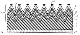
도 3 에 따른 광전지는 도 1 에 나타낸 광전지의 다층 스택과 실질적으로 유사한 다층 스택을 가진다. 하지만, 도 3 에서는, 실리콘의 결정질 산화물 박막 (11) 이 결정질 실리콘 기판 (1) 과 얇은 진성 비정질 실리콘층 (2) 사이에 성막된다.
그런 다음, 박막 (11) 에 의하여 형성된 유닛, 진성 비정질 실리콘층 (2), p-도핑된 비정질 실리콘층 (3), 전극 (4) 및 집전 장치 (5) 는 기판 (1) 의 정면 (1a) 에 배열된 다층 스택을 구성하고, 도 3 에서 A1 으로 나타낸다.
보다 구체적으로는, 박막 (11) 은 상기 기판 (1) 과 진성 비정질 실리콘층 (2) 사이에 n-도핑된 결정질 실리콘의 기판 (1) 의 정면 (1a) 에 직접적으로 배열된다. 그 결과로서, 박막은 기판 (1) 의 정면 (1a) 과 직접적으로 접촉한다. 게다가, 유리하게는, 박막은 2 나노미터 이하의 두께, 또한 유리하게는 0.1nm 와 2nm 사이의 두께 및 통상적으로 약 0.5nm 의 두께를 가진다.
보다 구체적으로는, 스택 (A1) 의 연속적인 얇은 층들 (2, 3, 4 및 5) 의 형성 이전에, 박막 (11) 은 기판 (1) 의 표면 부분의 실리콘을 산화함으로써 얻어지는 박막이다. 기판 (1) 의 표면 부분에 의하여, 박막은 매우 낮은 두께 (유리하게는, 2nm 미만) 로, 기판 (1) 의 자유면으로부터 기판의 내부로 신장하는, 기판 (1) 의 영역으로 이해된다. 게다가, 박막 (11) 은 실리콘의 결정질 산화물, 즉 결정형의 산화물로 구성된다. 특히, 특정한 경우들에서, 실리콘 산화물의 결정형은 결정면 (100) 을 갖는 실리콘 기판에 대한 트리디마이트 (tridymite) 형태일 수 있는 것으로 가정된다.
게다가, 상기 산화는 라디칼 표면 산화, 즉 라디칼들 (또는 자유 라디칼들) 에 의하여 수행된 산화이다. 특히, 이러한 라디칼들은, 예컨대 산소, 오존 및/또는 물로부터 얻어지는, 산소화된 라디칼들이다.
그런 다음, 이렇게 얻어진 라디칼들은 기판 (1) 의 표면 부분에 실리콘을 산화시킨다. 게다가, 라디칼 산화 중 이와 같이 얻어진 실리콘 산화물은 적어도 부분적으로 결정형이다. 보다 구체적으로는, 실리콘 기판의 라디칼 표면 산화는 실리콘 기판의 표면에 상기 결정질 박막을 형성하기 위하여 유리하게 조절된다. 하지만, 특정한 경우들에서, 기판의 라디칼 표면 산화는 비정질형의 실리콘 산화물의, 실리콘의 결정질 산화물 상의, 추가의 형성을 포함할 수 있다. 하지만, 박막 (11) 을 형성하는 실리콘의 결정질 산화물이 기판 (11) 과 비정질 실리콘 산화물 사이에 개재되어 유지된다. 게다가, 라디칼 표면 산화 동안 유리하게 형성된 비정질 실리콘 산화물은 라디칼 표면 산화의 뒤를 잇는 중간 단계 동안, 보다 구체적으로는, 스택 (A1) 의 다른 층들의 형성 이전에, 스트리핑 (stripping) 에 의하여 가능한 한 제거될 수 있다.
유리하게, 산화될 기판의 표면에 자외선을 조사함으로써 또는 플라즈마에 의하여 산화를 돕는다. 플라즈마 또는 자외선 처리는, 특히 기판 (1) 의 실리콘을 산화시키기 위하여 사용된 자유 라디칼들의 형성을 용이하게 한다. 보다 구체적으로는, 이들은 처리의 형태에 따라 Oㆍ, O2 ㆍ, 및/또는 OHㆍ 형태의 라디칼들이고, 특히 산소 및/또는 오존 및/또는 물로부터 얻어진다.
특정한 실시형태에 따라, 기판 (1) 의 표면 부분의 산화는 범위가 160 nm ~ 400 nm 에 이르는 파장들을 가진 자외선 및 산소로부터 실시될 수 있다. 예컨대, 사용된 자외선의 파장들은 대략 185 nm 그리고 대략 254 nm 이다. 이러한 특정한 실시형태에서, 산소는 자외선의 작용 하에서, 자유 라디칼들 Oㆍ 로 그리고 오존으로 해리된다. 자유 라디칼들은 실리콘 표면을 산화시킬 수 있다.
게다가, 산화 작동중 온도는 주위 온도와 대략 900℃ 사이에 포함될 수 있으면서, 압력은 대략 10-4 와 대략 105 Pa 사이에 포함될 수 있다. 하지만, 유리한 방법으로, 온도와 압력은 각각 주위 온도와 주위 압력이다.
일단 박막 (11) 이 형성되면, 적어도 하나의 광전지를 제조하는 방법은 박층들의 연속적인 성막을 계속한다. 특히, 도 3 에 나타낸 실시형태에서, 박막 (11) 의 형성은 이하의 연속적인 성막들이 후속된다:
- 얇은 진성 비정질 실리콘층 (2) 의 성막,
- 상기 박막 (11) 상으로의 p-도핑된 얇은 비정질 실리콘층 (3) 의 성막,
- 층 (3) 상으로의 전극 (4) 의 성막,
- 전극 (4) 상으로의 집전 장치 (5) 의 성막, 및
- 기판 (1) 의 후면 (1b) 상으로의 전극 (6) 의 성막.
전술된 바와 같이, 라디칼 산화 작동중 박막 (11) 상에 형성가능한 비정질 실리콘 산화물을 제거하기 위한 중간 단계는 상기 얇은 층들의 연속 성막 이전에 실시될 수 있다.
따라서, 기판 (1) 의 표면들 중 하나에 실리콘의 결정질 산화물 박막을 형성시키면, 특히, 라디칼 산화가 실시될 때, 실리콘의 결정질 산화물이 매우 양호한 진성 품질을 갖는 중요한 부동화 특성들을 얻을 수 있음에 주목하였다. 따라서, 이러한 실리콘의 결정질 산화물 박막은 재결합하는 동안 전하 운반체들이 포획 (trap) 되는 것을 방지하는 것을 가능하게 한다. 따라서, 이는 기판 (1) 의 표면 부동화를 보장함으로써 터널 산화물 (tunnel oxide) 역할을 한다. 따라서, 광전지의 개방 회로 장력을 증가시킬 수 있고, 잠재적으로 출력의 저하 없이 셀의 폼 팩터 (form factor) 를 다양하게 하고 단락 전류를 증폭시킬 수 있다.
게다가, 하나 이상의 광전지들의 제조 방법을 용이하게 할 수 있다. 실제로, 산화물의 박막으로 이와 같이 덮여진 기판 (1) 의 표면은, 제조 방법의 다음 단계들 (다른 얇은 층들의 성막) 을 실행하기 이전에, 가능한 대기 시간을 증가시킬 수 있는 보다 긴 지속 기간 동안 안정적이다. 게다가, 특정한 경우들에서 그리고 세정 상태들에 따라, 실리콘의 결정질 산화물 박막의 형성 이전에, 기판 (1) 의 표면에 존재하는 자연 산화막을 제거하는 것은 불필요하다. 후자는 특정한 상태들 하에서 라디칼 산화의 단계 동안 결정질 형태로 변형될 수 있다. 마지막으로, 부동화 층으로서 적어도 하나의 실리콘의 결정질 산화물 박막을 형성한다는 사실은, 진성 비정질 실리콘을 성막시키기 이전에 불화수소산으로 기판을 세정하는 단계로부터 처리를 자유롭게 할 수 있어, 처리 안정성이 향상될 수 있다.
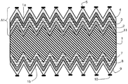
도 3 에 있어서, 기판 (1) 의 후면 (1b) 은 평평하고, 도 1 에 따른 실시 형태에서와 같이, 전극 (6) 으로 덮여진다. 반면에, 도 4 에 도시된 바와 같이, 후면 (1b) 은 도 2 에 도시된 바와 같이 조직화 (textured) 될 수 있고, 다층 스택으로, 즉
- 진성 비정질 실리콘층 (7),
- 예컨대, n-도핑으로 매우 강하게 도핑된 비정질 실리콘층 (8),
- 예컨대, ITO 로 구성된 전극 (9),
- 그리고 빗 (comb) 형태의 집전 장치 (10) 에 의해 균일하게 그리고 연속하여 덮여질 수 있다.
게다가, 특정한 실시형태들에 있어서, 추가의 박막 (12) 이 기판 (1) 의 후면 (1b) 위에 성막될 수 있다.
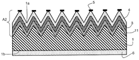
따라서, 대안의 실시형태에 따라서 그리고 도 5 에 도시된 바와 같이, 셀은 도 3 및 도 4 에서 도시된 다층 스택과 동일한 다층 스택 (A1) 으로 덮여진 정면 (1a) 을 포함할 수 있다. 반면에, 정면 (1a) 과 같이, 기판 (1) 의 후면 (1b) 은 조직화되고, 게다가, 추가의 실리콘의 결정질 산화물 박막 (12) 으로 덮여진다. 상기 추가의 박막 (12) 은 얇은 진성 비정질층 (7), n-도핑된 얇은 비정질 실리콘층 (8), 전극 (9) 및 집전 장치 (10) 로 형성된 다층 스택으로 덮여지고, 그런 다음 유닛은 기판 (1) 의 후면 (1b) 을 덮는 다층 스택을 형성하고, 도 5 에서 B1 으로 나타낸다.
특정한 경우들에서, 실리콘의 결정질 산화물의 매우 양호한 진성 품질은 우수한 표면 부동화를 얻기에 충분하고, 상기 박막과 도핑된 얇은 비정질 실리콘층 사이에 진성 비정질 실리콘의 얇은 부동화 층 (2) 의 필요성을 제거할 수 있다.
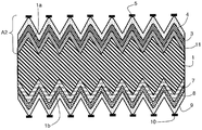
그런 다음, 박막 (11) 은 기판 (1) 과 p-도핑된 비정질 실리콘층 (3) 사이에 직접 성막될 수 있다. 따라서, 이러한 실시형태들에서, 다층 스택 (A1) 을 박막 (11) 과 p-도핑된 얇은 비정질 실리콘층 (3) 사이의 얇은 진성 실리콘층 (2) 을 제거하는 스택 (A1) 과 상이한 다층 스택 (A2) 으로 교체하는 것이 예상될 수 있다. 그런 다음, 이러한 스택 (A2) 은 도 6 ~ 도 9 에 도시된 바와 같이 기판 (1) 의 후면 (1b) 에 대한 다양한 실시형태들과 연관될 수 있다.
따라서, 도 6 에서, 기판 (1) 의 정면 (1a) 를 덮는 상기 스택 (A2) 은, 기판 (1) 의 평평한 후면 (1b) 을 덮는 전극 (6) 과 연관된다.
도 7 에서, 후면 (1b) 은 기판 (1) 의 정면 (1a) 과 같이 조직화되고, 도 2 에 나타낸 것과 같은 다층 스택, 즉 추가의 실리콘의 결정질 산화물 박막 (12) 을 포함하지 않는 다층 스택으로 덮여진다.
도 8 에서, 기판 (1) 의 후면 (1b) 은 기판의 정면 (1a) 과 같이 또한 조직화되고, 다층 스택 (B1), 즉 기판 (1) 과 n-도핑된 얇은 비정질 실리콘층 (8) 사이에 삽입된 추가의 박막 (12) 을 포함하는 스택으로 덮여진다.
마지막으로, 도 9 에서, 기판 (1) 의 후면 (1b) 은 기판의 정면 (1b) 과 같이 또한 조직화되고, 다층 스택 (B2) 으로 덮여진다. 다층 스택 (B2) 은, 추가의 박막 (12) 과 비정질 실리콘층 (8) 사이에 배열된 진성 비정질 실리콘층 (7) 을 포함하지 않는 스택 (B1) 과 상이하다.
광전지가 기판 (1) 의 후면 (1b) 에 배열된 추가의 박막 (12) 뿐만 아니라 기판 (1) 의 정면 (1a) 에 배열된 박막 (11) 을 포함할 때, 2 개의 박막들 (11, 12) 은 동시적인 방법으로, 또는 연속적인 방법으로 실현될 수 있다.
이 경우에, 2 개의 박막들 (11, 12) 은 연속적인 방법으로 실현되고, 광전지는 이하와 같이 유리하게 구성될 수 있다:
- 박막 (11), 가능한 한 얇은 진성 비정질 실리콘층 (2) 및 p-도핑된 비정질 실리콘층 (3) 은 이형접합을 형성하기 위하여 기판 (1) 의 정면 (1a) 에 연속적으로 형성되고,
- 그런 다음, 추가의 박막 (12), 가능한 한 얇은 진성 비정질 실리콘층 (7) 및 n-도핑된 비정질 실리콘층 (8) 은 기판 (1) 의 후면 (1b) 에 연속적으로 형성되고,
- 그리고, 마지막으로, 전극들 (4 및 9) 및 상기 전극들 (4 및 9) 과 각각 연결된 집전 장치들 (5 및 10) 은 이들 각각의 스택 상에 형성된다.
유리하게는, 각각의 2 개의 박막들 (11 및 12) 은, 산소화된 라디칼들과 같은 자유 라디칼들에 의해 라디칼 산화로 그리고 가능하게는 플라즈마 처리 또는 자외선의 도움으로 구성된다.
다른 대안의 실시형태에 따라, 광전지는 또한 기판 (1) 의 정면 (1a) 상에 위치되는 것 (도 3, 4, 6 및 7 의 경우들) 이 아니라, 기판 (1) 의 후면 (1b) 상에 위치되는 단 하나의 실리콘의 결정질 산화물 박막을 포함할 수 있다. 실리콘의 결정질 산화물 박막은 항상 산소화된 라디칼들에 의하여 그리고 가능하게는 플라즈마 처리 또는 자외선의 도움으로 라디칼 산화에 의해 유리하게 구성된다. 이러한 경우에서, 정면 (1a) 은 기판 (1) 과 p-도핑된 얇은 비정질 실리콘층 (3) 사이에 배열된 얇은 진성 비정질 실리콘층 (2) 으로 유리하게 덮여진다. 후면 (1b) 은 실리콘의 결정질 산화물 박막과 도핑된 결정질 실리콘층 (8) 사이에 얇은 진성 비정질 실리콘층 (7) 을 포함할 수 있거나 포함할 수 없다.
본 발명은 전술한 실시형태들, 특히 기판 (1) 의 도핑 형태 (n 또는 p) 와 도핑된 비정질 실리콘층 (3 및 8) 에 관하여 한정되지 않는다.
결과적으로, 본 발명은, 각각 p-도핑된 그리고 n-도핑된 비정질 실리콘층들 (3 및 8) 과 n-도핑된 결정질 실리콘 기판을 포함하는 실시형태들에 한정되지 않는다. 비정질 실리콘층 (3) 은 이형접합을 형성하기 위하여 기판 (1) 의 도핑 형태 (n 또는 p) 에 반대되는 도핑 형태 (p 또는 n) 를 가져야만 하고, 기판 (1) 의 후면 (1b) 의 측면 상에 배열된 비정질 실리콘층 (8) 은 기판 (1) 의 도핑 형태 (n 또는 p) 와 같은 도핑 형태 (n 또는 p) 를 가져야만 한다.
게다가, 비정질 실리콘으로 구성되는 대신에, 얇은 층들 (3 및 8) 은 또한 미세 결정질 실리콘으로 구성될 수 있다.
마지막으로, 진성 비정질 실리콘층들 (2 및 7) 을 사용하는 대신에, 상기 층 (2 또는 7) 에 배열되도록 의도된 비정질 실리콘층 (3 또는 8) 의 도핑 형태와 같은 도핑 형태로 미세 도핑된 (microdopped) 비정질 실리콘으로 또한 불려지는, 약간 도핑된 비정질 실리콘을 사용할 수 있다. 약간 도핑된 또는 미세 도핑된 비정질 실리콘에 의하여, 도핑은 일반적으로 사용된 도핑 레벨보다 실질적으로 낮다는 것으로 이해된다. 따라서, 실시예와 같이, 각각의 비정질 실리콘층들 (2 및 7) 의 도핑제들의 농도는 1×10¹⁶ ~ 1×10¹⁸ at/cm3 사이일 수 있는 반면에, 각각의 비정질 실리콘의 얇은 층들 (3 및 8) 은 1×10¹⁹ at.cm3 ~ 1×10²² at.cm3 사이의 도핑제들의 농도를 가질 수 있다.
미세 도핑된 비정질 실리콘으로 진성 비정질 실리콘을 교체하는 것은, 낮은 도핑 레벨 때문에, 낮은 국부적인 상태 밀도, 따라서 높은 개방 회로 장력뿐만 아니라 기판과 계면에서의 캐리어들의 낮은 재결합률을 얻는 것을 허용한다. 게다가, 미세 도핑된 비정질층은, 셀의 직렬 저항을 감소시키고 셀의 폼 팩터를 실질적으로 향상시키는 진성 비정질 층의 전도도보다 실질적으로 더 높은 전도도를 가진다.
Claims (18)
- 주어진 도핑 형태를 가진 결정질 실리콘 기판 (1) 과 비정질 또는 미세 결정질 실리콘층 (3, 8) 을 포함하는 이형접합 광전지에 있어서,
상기 기판 (1) 과 상기 비정질 또는 미세 결정질 실리콘층 (3, 8) 사이에, 상기 기판 (1) 의 면 (1a, 1b) 위에 직접 배치되는 적어도 하나의 실리콘의 결정질 산화물 박막 (11) 을 포함하는 것을 특징으로 하는 이형접합 광전지. - 제 1 항에 있어서,
상기 실리콘의 결정질 산화물 박막 (11) 은, 라디칼들에 의해 산화되는 상기 기판 (1) 의 표면부로 구성되는 것을 특징으로 하는 이형접합 광전지. - 제 1 항 또는 제 2 항에 있어서,
상기 실리콘의 결정질 산화물 박막 (11) 은 2 나노미터 이하의 두께를 가지는 것을 특징으로 하는 이형접합 광전지. - 제 1 항 내지 제 3 항 중 어느 한 항에 있어서,
상기 실리콘의 결정질 산화물 박막 (11) 과 상기 비정질 또는 미세 결정질 실리콘층 (3, 8) 사이에 얇은 진성 (intrinsic) 또는 미세 도핑된 비정질 실리콘층 (2, 7) 이 개재된 것을 특징으로 하는 이형접합 광전지. - 제 1 항 내지 제 3 항 중 어느 한 항에 있어서,
상기 실리콘의 결정질 산화물 박막 (11) 은 상기 비정질 또는 미세 결정질 실리콘층 (3, 8) 과 직접 접촉하는 것을 특징으로 하는 이형접합 광전지. - 제 1 항 내지 제 5 항 중 어느 한 항에 있어서,
상기 비정질 또는 미세 결정질 실리콘층 (8) 은 상기 결정질 실리콘 기판 (1) 의 도핑 형태와 동일한 도핑 형태를 갖는 것을 특징으로 하는 이형접합 광전지. - 제 1 항 내지 제 5 항 중 어느 한 항에 있어서,
상기 비정질 또는 미세 결정질 실리콘층 (3) 은 상기 결정질 실리콘 기판 (1) 의 도핑 형태와 반대되는 도핑 형태를 갖는 것을 특징으로 하는 이형접합 광전지. - 제 7 항에 있어서,
상기 기판 (1) 과 추가의 비정질 또는 미세 결정질 실리콘층 (8) 사이에, 상기 기판 (1) 의 다른 면 (1b) 에 직접 배열되는 추가의 실리콘의 결정질 산화물 박막 (12) 을 포함하고, 상기 추가의 비정질 또는 미세 결정질 실리콘층 (8) 은 상기 결정질 실리콘 기판 (1) 의 도핑 형태와 동일한 도핑 형태를 갖는 것을 특징으로 하는 이형접합 광전지. - 제 8 항에 있어서,
상기 추가의 실리콘의 결정질 산화물 박막 (12) 과 상기 추가의 비정질 또는 미세 결정질 실리콘층 (8) 사이에 추가의 얇은 진성 또는 미세 도핑된 비정질 실리콘층 (7) 이 개재된 것을 특징으로 하는 이형접합 광전지. - 제 8 항에 있어서,
상기 추가의 실리콘의 결정질 산화물 박막 (12) 은 상기 추가의 비정질 또는 미세 결정질 실리콘층 (8) 과 직접 접촉하는 것을 특징으로 하는 이형접합 광전지. - 제 1 항 내지 제 10 항 중 어느 한 항에 있어서,
상기 결정질 실리콘 기판 (1) 의 적어도 하나의 면 (1a, 1b) 이 조직화 (textured) 되는 것을 특징으로 하는 이형접합 광전지. - 제 1 항 내지 제 11 항 중 어느 한 항에 있어서,
상기 박막과 상기 비정질 또는 미세 결정질 실리콘층 (3, 8) 사이에서, 상기 실리콘의 결정질 산화물 박막 (11, 12) 에 비정질 실리콘 산화물층이 직접 배열되는 것을 특징으로 하는 이형접합 광전지. - 제 1 항 내지 제 12 항 중 어느 한 항에 따른 적어도 하나의 광전지의 제조 방법에 있어서,
실리콘의 결정질 산화물 박막 (11, 12) 은, 상기 비정질 또는 미세 결정질 실리콘층 (3, 8) 의 형성 이전에, 상기 기판 (1) 의 표면의 라디칼 표면 산화에 의해 만들어지는 것을 특징으로 하는 광전지 제조 방법. - 제 13 항에 있어서,
상기 라디칼 표면 산화는 산소 및/또는 오존 및/또는 물로부터 얻어진 산소화된 라디칼들에 의하여 실시되는 것을 특징으로 하는 광전지 제조 방법. - 제 14 항에 있어서,
상기 기판 (1) 의 표면의 표면 산화는 상기 표면에 자외선들을 가함으로써 보조되는 것을 특징으로 하는 광전지 제조 방법. - 제 15 항에 있어서,
상기 산소화된 라디칼들은 적어도 산소로부터 얻어지고, 상기 자외선들은 160 nm 와 400 nm 사이의 범위에 있는 파장들을 갖는 것을 특징으로 하는 광전지 제조 방법. - 제 13 항 또는 제 14 항에 있어서,
상기 기판 (1) 의 표면의 상기 표면 산화는 플라즈마로 보조되는 것을 특징으로 하는 광전지 제조 방법. - 제 13 항 내지 제 17 항 중 어느 한 항에 있어서,
상기 기판 (1) 의 표면의 상기 라디칼 표면 산화에 후속하여, 상기 박막 (11, 12) 의 상기 표면에 비정질 형태로 라디칼 표면 산화 중에 형성되는 실리콘 산화물의 일부를 제거하는 스트리핑 단계가 실시되는 것을 특징으로 하는 광전지 제조 방법.
Applications Claiming Priority (3)
| Application Number | Priority Date | Filing Date | Title |
|---|---|---|---|
| FR1000309A FR2955702B1 (fr) | 2010-01-27 | 2010-01-27 | Cellule photovoltaique comprenant un film mince de passivation en oxyde cristallin de silicium et procede de realisation |
| FR1000309 | 2010-01-27 | ||
| PCT/FR2011/000050 WO2011092402A2 (fr) | 2010-01-27 | 2011-01-26 | Cellule photovoltaïque comprenant un film mince de passivation en oxyde cristallin de silicium et procédé de réalisation |
Publications (1)
| Publication Number | Publication Date |
|---|---|
| KR20120127613A true KR20120127613A (ko) | 2012-11-22 |
Family
ID=43092832
Family Applications (1)
| Application Number | Title | Priority Date | Filing Date |
|---|---|---|---|
| KR1020127022105A KR20120127613A (ko) | 2010-01-27 | 2011-01-26 | 실리콘의 결정질 산화물 부동화 박막을 포함하는 광전지 및 그 제조 방법 |
Country Status (8)
| Country | Link |
|---|---|
| US (1) | US10276738B2 (ko) |
| EP (1) | EP2529416B1 (ko) |
| JP (2) | JP2013518426A (ko) |
| KR (1) | KR20120127613A (ko) |
| CN (1) | CN102770972B (ko) |
| ES (1) | ES2560216T3 (ko) |
| FR (1) | FR2955702B1 (ko) |
| WO (1) | WO2011092402A2 (ko) |
Cited By (5)
| Publication number | Priority date | Publication date | Assignee | Title |
|---|---|---|---|---|
| KR20140112649A (ko) * | 2013-03-13 | 2014-09-24 | 엘지전자 주식회사 | 태양전지 |
| KR20140115435A (ko) * | 2013-03-19 | 2014-10-01 | 엘지전자 주식회사 | 태양전지 |
| KR101867969B1 (ko) * | 2017-01-18 | 2018-06-15 | 엘지전자 주식회사 | 이종 접합 태양전지 |
| KR101886818B1 (ko) * | 2018-07-25 | 2018-08-08 | 충남대학교산학협력단 | 이종 접합 실리콘 태양 전지의 제조 방법 |
| KR20190008390A (ko) * | 2016-11-23 | 2019-01-23 | 엘지전자 주식회사 | 태양 전지 및 이의 제조 방법 |
Families Citing this family (24)
| Publication number | Priority date | Publication date | Assignee | Title |
|---|---|---|---|---|
| JP5824681B2 (ja) * | 2011-06-30 | 2015-11-25 | パナソニックIpマネジメント株式会社 | 光起電力装置 |
| KR101430054B1 (ko) * | 2012-09-20 | 2014-08-18 | 한국기술교육대학교 산학협력단 | 결정질 실리콘 태양전지의 제조 방법 |
| FR2996059B1 (fr) * | 2012-09-24 | 2015-06-26 | Commissariat Energie Atomique | Procede de realisation d'une cellule photovoltaique a heterojonction et cellule photovoltaique ainsi obtenue |
| KR101925929B1 (ko) * | 2013-01-16 | 2018-12-06 | 엘지전자 주식회사 | 태양 전지 및 그의 제조 방법 |
| KR101925928B1 (ko) * | 2013-01-21 | 2018-12-06 | 엘지전자 주식회사 | 태양 전지 및 그의 제조 방법 |
| KR20160090287A (ko) * | 2013-09-27 | 2016-07-29 | 덴마크스 텍니스케 유니버시테트 | 나노구조의 실리콘계 태양 전지 및 나노구조의 실리콘계 태양 전지의 제조 방법 |
| FR3015770B1 (fr) | 2013-12-19 | 2016-01-22 | Commissariat Energie Atomique | Procede et systeme de controle de qualite de cellules photovoltaiques |
| JP2015138829A (ja) * | 2014-01-21 | 2015-07-30 | 長州産業株式会社 | 太陽電池モジュール |
| US20150380581A1 (en) * | 2014-06-27 | 2015-12-31 | Michael C. Johnson | Passivation of light-receiving surfaces of solar cells with crystalline silicon |
| AU2015283813B2 (en) * | 2014-07-02 | 2021-01-07 | Sundrive Solar Pty Ltd | A method for forming a photovoltaic cell and a photovoltaic cell formed according to the method |
| US9812448B2 (en) | 2014-12-17 | 2017-11-07 | Samsung Electronics Co., Ltd. | Semiconductor devices and methods for fabricating the same |
| CN104576803B (zh) * | 2015-01-21 | 2016-10-12 | 中电投西安太阳能电力有限公司 | 基于GaN纳米线三维结构的太阳能电池及其制备方法 |
| CN105990470B (zh) * | 2015-03-06 | 2017-06-16 | 新日光能源科技股份有限公司 | 异质结太阳能电池及其制造方法 |
| CN106024964B (zh) * | 2016-07-13 | 2017-09-22 | 北京工业大学 | 一种n型背结双面太阳电池的制备方法 |
| CN106252424A (zh) * | 2016-08-24 | 2016-12-21 | 常州天合光能有限公司 | 热氧化改善钝化层界面的异质结电池及其制备方法 |
| WO2018061769A1 (ja) * | 2016-09-27 | 2018-04-05 | パナソニックIpマネジメント株式会社 | 太陽電池セルおよび太陽電池セルの製造方法 |
| US10861694B2 (en) * | 2017-01-17 | 2020-12-08 | Zf Friedrichshafen Ag | Method of manufacturing an insulation layer on silicon carbide |
| KR102514785B1 (ko) * | 2017-05-19 | 2023-03-29 | 상라오 징코 솔라 테크놀러지 디벨롭먼트 컴퍼니, 리미티드 | 태양 전지 및 이의 제조 방법 |
| GB2565056A (en) * | 2017-07-28 | 2019-02-06 | Comptek Solutions Oy | Semiconductor device and method of manufacture |
| CN108054219A (zh) * | 2017-12-15 | 2018-05-18 | 浙江晶科能源有限公司 | 一种p型太阳能电池及其制作方法 |
| CN112151636B (zh) * | 2020-08-21 | 2022-07-15 | 隆基绿能科技股份有限公司 | 硅基异质结太阳电池及其制备方法 |
| EP4307394A1 (en) * | 2021-05-18 | 2024-01-17 | Hengdian Group DMEGC Magnetics Co., Ltd. | Perc battery back passivation structure, and perc battery and preparation method therefor |
| CN113257927A (zh) * | 2021-05-18 | 2021-08-13 | 横店集团东磁股份有限公司 | 一种perc电池背钝化结构、perc电池及制备方法 |
| CN113937192A (zh) * | 2021-07-30 | 2022-01-14 | 国家电投集团科学技术研究院有限公司 | 硅异质结太阳电池非晶硅钝化层的制备方法 |
Family Cites Families (22)
| Publication number | Priority date | Publication date | Assignee | Title |
|---|---|---|---|---|
| US5057439A (en) * | 1990-02-12 | 1991-10-15 | Electric Power Research Institute | Method of fabricating polysilicon emitters for solar cells |
| JPH0738111A (ja) | 1993-07-22 | 1995-02-07 | Fujitsu Ltd | 薄膜トランジスタの形成方法 |
| JPH0766437A (ja) | 1993-08-30 | 1995-03-10 | Tonen Corp | 光電変換装置用基板の製造方法 |
| JPH0786271A (ja) * | 1993-09-17 | 1995-03-31 | Fujitsu Ltd | シリコン酸化膜の作製方法 |
| US6207890B1 (en) * | 1997-03-21 | 2001-03-27 | Sanyo Electric Co., Ltd. | Photovoltaic element and method for manufacture thereof |
| JP3233281B2 (ja) * | 1999-02-15 | 2001-11-26 | 日本電気株式会社 | ゲート酸化膜の形成方法 |
| US6890450B2 (en) | 2001-02-02 | 2005-05-10 | Intel Corporation | Method of providing optical quality silicon surface |
| US6916717B2 (en) | 2002-05-03 | 2005-07-12 | Motorola, Inc. | Method for growing a monocrystalline oxide layer and for fabricating a semiconductor device on a monocrystalline substrate |
| JP2005175023A (ja) * | 2003-12-08 | 2005-06-30 | National Institute Of Advanced Industrial & Technology | 高密度シリコン酸化膜、その製造方法およびそれを用いた半導体デバイス |
| US7554031B2 (en) * | 2005-03-03 | 2009-06-30 | Sunpower Corporation | Preventing harmful polarization of solar cells |
| JP2007194485A (ja) | 2006-01-20 | 2007-08-02 | Osaka Univ | 太陽電池用シリコン基板の製造方法 |
| EP1850378A3 (en) * | 2006-04-28 | 2013-08-07 | Semiconductor Energy Laboratory Co., Ltd. | Memory device and semicondutor device |
| US7737357B2 (en) * | 2006-05-04 | 2010-06-15 | Sunpower Corporation | Solar cell having doped semiconductor heterojunction contacts |
| NL2000248C2 (nl) * | 2006-09-25 | 2008-03-26 | Ecn Energieonderzoek Ct Nederl | Werkwijze voor het vervaardigen van kristallijn-silicium zonnecellen met een verbeterde oppervlaktepassivering. |
| JP2008300440A (ja) | 2007-05-29 | 2008-12-11 | Sanyo Electric Co Ltd | 太陽電池セル及び太陽電池モジュール |
| US20100275996A1 (en) * | 2007-11-30 | 2010-11-04 | Kaneka Corporation | Silicon-based thin-film photoelectric conversion device |
| JP5572307B2 (ja) * | 2007-12-28 | 2014-08-13 | 株式会社半導体エネルギー研究所 | 光電変換装置の製造方法 |
| TW200947725A (en) * | 2008-01-24 | 2009-11-16 | Applied Materials Inc | Improved HIT solar cell structure |
| WO2009120631A2 (en) * | 2008-03-25 | 2009-10-01 | Applied Materials, Inc. | Surface cleaning and texturing process for crystalline solar cells |
| US20090293954A1 (en) * | 2008-05-30 | 2009-12-03 | Semiconductor Energy Laboratory Co., Ltd. | Photoelectric Conversion Device And Method For Manufacturing The Same |
| US20100186802A1 (en) * | 2009-01-27 | 2010-07-29 | Peter Borden | Hit solar cell structure |
| JP5537101B2 (ja) | 2009-09-10 | 2014-07-02 | 株式会社カネカ | 結晶シリコン系太陽電池 |
-
2010
- 2010-01-27 FR FR1000309A patent/FR2955702B1/fr not_active Expired - Fee Related
-
2011
- 2011-01-26 US US13/522,901 patent/US10276738B2/en active Active
- 2011-01-26 ES ES11708521.7T patent/ES2560216T3/es active Active
- 2011-01-26 JP JP2012550488A patent/JP2013518426A/ja active Pending
- 2011-01-26 EP EP11708521.7A patent/EP2529416B1/fr active Active
- 2011-01-26 CN CN201180007552.XA patent/CN102770972B/zh active Active
- 2011-01-26 KR KR1020127022105A patent/KR20120127613A/ko active Search and Examination
- 2011-01-26 WO PCT/FR2011/000050 patent/WO2011092402A2/fr active Application Filing
-
2015
- 2015-08-03 JP JP2015153692A patent/JP2016006895A/ja active Pending
Cited By (5)
| Publication number | Priority date | Publication date | Assignee | Title |
|---|---|---|---|---|
| KR20140112649A (ko) * | 2013-03-13 | 2014-09-24 | 엘지전자 주식회사 | 태양전지 |
| KR20140115435A (ko) * | 2013-03-19 | 2014-10-01 | 엘지전자 주식회사 | 태양전지 |
| KR20190008390A (ko) * | 2016-11-23 | 2019-01-23 | 엘지전자 주식회사 | 태양 전지 및 이의 제조 방법 |
| KR101867969B1 (ko) * | 2017-01-18 | 2018-06-15 | 엘지전자 주식회사 | 이종 접합 태양전지 |
| KR101886818B1 (ko) * | 2018-07-25 | 2018-08-08 | 충남대학교산학협력단 | 이종 접합 실리콘 태양 전지의 제조 방법 |
Also Published As
| Publication number | Publication date |
|---|---|
| FR2955702A1 (fr) | 2011-07-29 |
| JP2013518426A (ja) | 2013-05-20 |
| FR2955702B1 (fr) | 2012-01-27 |
| US10276738B2 (en) | 2019-04-30 |
| ES2560216T3 (es) | 2016-02-17 |
| WO2011092402A2 (fr) | 2011-08-04 |
| JP2016006895A (ja) | 2016-01-14 |
| WO2011092402A3 (fr) | 2012-08-30 |
| EP2529416B1 (fr) | 2015-10-21 |
| CN102770972B (zh) | 2016-03-23 |
| CN102770972A (zh) | 2012-11-07 |
| EP2529416A2 (fr) | 2012-12-05 |
| US20120291861A1 (en) | 2012-11-22 |
Similar Documents
| Publication | Publication Date | Title |
|---|---|---|
| KR20120127613A (ko) | 실리콘의 결정질 산화물 부동화 박막을 포함하는 광전지 및 그 제조 방법 | |
| US8877539B2 (en) | Method for producing a photovoltaic cell including the preparation of the surface of a crystalline silicon substrate | |
| US9871161B2 (en) | Method for making crystalline silicon-based solar cell, and method for making solar cell module | |
| JP5421701B2 (ja) | 結晶シリコン太陽電池及びその製造方法 | |
| Suhail et al. | Improved efficiency of graphene/Si Schottky junction solar cell based on back contact structure and DUV treatment | |
| JP7331232B2 (ja) | 太陽電池及びその製造方法、太陽電池モジュール | |
| WO2012036146A1 (ja) | 結晶太陽電池及びその製造方法 | |
| US9905710B2 (en) | Solar cell | |
| Tucci et al. | 17% efficiency heterostructure solar cell based on p-type crystalline silicon | |
| JP2013239476A (ja) | 光起電力装置およびその製造方法、光起電力モジュール | |
| US20120273036A1 (en) | Photoelectric conversion device and manufacturing method thereof | |
| CN108475707B (zh) | 光电转换装置的制造方法 | |
| KR101086074B1 (ko) | 실리콘 나노 와이어 제조 방법, 실리콘 나노 와이어를 포함하는 태양전지 및 태양전지의 제조 방법 | |
| JP2012049156A (ja) | 太陽電池およびその製造方法 | |
| JP5948148B2 (ja) | 光電変換装置 | |
| CN115188837A (zh) | 一种背接触太阳能电池及制备方法、电池组件 | |
| JP5307688B2 (ja) | 結晶シリコン系太陽電池 | |
| WO2014134515A1 (en) | High-efficiency, low-cost silicon-zinc oxide heterojunction solar cells | |
| JP2014082285A (ja) | 太陽電池およびその製造方法、太陽電池モジュール | |
| CN108431967B (zh) | 光电转换装置的制造方法 | |
| JP2017005270A (ja) | 光電変換装置の作製方法 | |
| Tucci et al. | CF4/O2 dry etching of textured crystalline silicon surface in a-Si: H/c-Si heterojunction for photovoltaic applications | |
| WO2017010029A1 (ja) | 光電変換装置 | |
| TWI443852B (zh) | 太陽能電池形成方法 | |
| CN110809827A (zh) | 光电转换装置的制造方法 |
Legal Events
| Date | Code | Title | Description |
|---|---|---|---|
| AMND | Amendment | ||
| A201 | Request for examination | ||
| AMND | Amendment | ||
| E902 | Notification of reason for refusal | ||
| AMND | Amendment | ||
| E601 | Decision to refuse application | ||
| AMND | Amendment |