JP6759784B2 - 半導体モジュール - Google Patents
半導体モジュール Download PDFInfo
- Publication number
- JP6759784B2 JP6759784B2 JP2016137730A JP2016137730A JP6759784B2 JP 6759784 B2 JP6759784 B2 JP 6759784B2 JP 2016137730 A JP2016137730 A JP 2016137730A JP 2016137730 A JP2016137730 A JP 2016137730A JP 6759784 B2 JP6759784 B2 JP 6759784B2
- Authority
- JP
- Japan
- Prior art keywords
- semiconductor chip
- metal bonding
- insulating layer
- semiconductor
- bonding material
- Prior art date
- Legal status (The legal status is an assumption and is not a legal conclusion. Google has not performed a legal analysis and makes no representation as to the accuracy of the status listed.)
- Active
Links
- 239000004065 semiconductor Substances 0.000 title claims description 107
- 229910052751 metal Inorganic materials 0.000 claims description 73
- 239000002184 metal Substances 0.000 claims description 73
- 239000000463 material Substances 0.000 claims description 63
- 239000000758 substrate Substances 0.000 claims description 24
- 229910018072 Al 2 O 3 Inorganic materials 0.000 claims description 2
- 230000017525 heat dissipation Effects 0.000 description 18
- 238000006243 chemical reaction Methods 0.000 description 13
- 229910000679 solder Inorganic materials 0.000 description 9
- 239000000919 ceramic Substances 0.000 description 2
- 230000006866 deterioration Effects 0.000 description 2
- 238000010586 diagram Methods 0.000 description 2
- 238000009413 insulation Methods 0.000 description 2
- 230000000704 physical effect Effects 0.000 description 2
- 239000004020 conductor Substances 0.000 description 1
- PMHQVHHXPFUNSP-UHFFFAOYSA-M copper(1+);methylsulfanylmethane;bromide Chemical compound Br[Cu].CSC PMHQVHHXPFUNSP-UHFFFAOYSA-M 0.000 description 1
- 230000007423 decrease Effects 0.000 description 1
- 230000001771 impaired effect Effects 0.000 description 1
- 238000004519 manufacturing process Methods 0.000 description 1
- 238000005498 polishing Methods 0.000 description 1
- 238000004904 shortening Methods 0.000 description 1
Images


Classifications
-
- H—ELECTRICITY
- H01—ELECTRIC ELEMENTS
- H01L—SEMICONDUCTOR DEVICES NOT COVERED BY CLASS H10
- H01L23/00—Details of semiconductor or other solid state devices
- H01L23/34—Arrangements for cooling, heating, ventilating or temperature compensation ; Temperature sensing arrangements
- H01L23/36—Selection of materials, or shaping, to facilitate cooling or heating, e.g. heatsinks
- H01L23/367—Cooling facilitated by shape of device
- H01L23/3675—Cooling facilitated by shape of device characterised by the shape of the housing
-
- H—ELECTRICITY
- H01—ELECTRIC ELEMENTS
- H01L—SEMICONDUCTOR DEVICES NOT COVERED BY CLASS H10
- H01L23/00—Details of semiconductor or other solid state devices
- H01L23/34—Arrangements for cooling, heating, ventilating or temperature compensation ; Temperature sensing arrangements
- H01L23/36—Selection of materials, or shaping, to facilitate cooling or heating, e.g. heatsinks
- H01L23/373—Cooling facilitated by selection of materials for the device or materials for thermal expansion adaptation, e.g. carbon
- H01L23/3735—Laminates or multilayers, e.g. direct bond copper ceramic substrates
-
- H—ELECTRICITY
- H01—ELECTRIC ELEMENTS
- H01L—SEMICONDUCTOR DEVICES NOT COVERED BY CLASS H10
- H01L23/00—Details of semiconductor or other solid state devices
- H01L23/02—Containers; Seals
- H01L23/04—Containers; Seals characterised by the shape of the container or parts, e.g. caps, walls
-
- H—ELECTRICITY
- H01—ELECTRIC ELEMENTS
- H01L—SEMICONDUCTOR DEVICES NOT COVERED BY CLASS H10
- H01L23/00—Details of semiconductor or other solid state devices
- H01L23/02—Containers; Seals
- H01L23/04—Containers; Seals characterised by the shape of the container or parts, e.g. caps, walls
- H01L23/043—Containers; Seals characterised by the shape of the container or parts, e.g. caps, walls the container being a hollow construction and having a conductive base as a mounting as well as a lead for the semiconductor body
- H01L23/049—Containers; Seals characterised by the shape of the container or parts, e.g. caps, walls the container being a hollow construction and having a conductive base as a mounting as well as a lead for the semiconductor body the other leads being perpendicular to the base
-
- H—ELECTRICITY
- H01—ELECTRIC ELEMENTS
- H01L—SEMICONDUCTOR DEVICES NOT COVERED BY CLASS H10
- H01L23/00—Details of semiconductor or other solid state devices
- H01L23/02—Containers; Seals
- H01L23/04—Containers; Seals characterised by the shape of the container or parts, e.g. caps, walls
- H01L23/053—Containers; Seals characterised by the shape of the container or parts, e.g. caps, walls the container being a hollow construction and having an insulating or insulated base as a mounting for the semiconductor body
-
- H—ELECTRICITY
- H01—ELECTRIC ELEMENTS
- H01L—SEMICONDUCTOR DEVICES NOT COVERED BY CLASS H10
- H01L23/00—Details of semiconductor or other solid state devices
- H01L23/34—Arrangements for cooling, heating, ventilating or temperature compensation ; Temperature sensing arrangements
- H01L23/36—Selection of materials, or shaping, to facilitate cooling or heating, e.g. heatsinks
-
- H—ELECTRICITY
- H01—ELECTRIC ELEMENTS
- H01L—SEMICONDUCTOR DEVICES NOT COVERED BY CLASS H10
- H01L24/00—Arrangements for connecting or disconnecting semiconductor or solid-state bodies; Methods or apparatus related thereto
-
- H—ELECTRICITY
- H01—ELECTRIC ELEMENTS
- H01L—SEMICONDUCTOR DEVICES NOT COVERED BY CLASS H10
- H01L24/00—Arrangements for connecting or disconnecting semiconductor or solid-state bodies; Methods or apparatus related thereto
- H01L24/01—Means for bonding being attached to, or being formed on, the surface to be connected, e.g. chip-to-package, die-attach, "first-level" interconnects; Manufacturing methods related thereto
- H01L24/26—Layer connectors, e.g. plate connectors, solder or adhesive layers; Manufacturing methods related thereto
- H01L24/31—Structure, shape, material or disposition of the layer connectors after the connecting process
- H01L24/32—Structure, shape, material or disposition of the layer connectors after the connecting process of an individual layer connector
-
- H—ELECTRICITY
- H01—ELECTRIC ELEMENTS
- H01L—SEMICONDUCTOR DEVICES NOT COVERED BY CLASS H10
- H01L25/00—Assemblies consisting of a plurality of individual semiconductor or other solid state devices ; Multistep manufacturing processes thereof
- H01L25/03—Assemblies consisting of a plurality of individual semiconductor or other solid state devices ; Multistep manufacturing processes thereof all the devices being of a type provided for in the same subgroup of groups H01L27/00 - H01L33/00, or in a single subclass of H10K, H10N, e.g. assemblies of rectifier diodes
- H01L25/04—Assemblies consisting of a plurality of individual semiconductor or other solid state devices ; Multistep manufacturing processes thereof all the devices being of a type provided for in the same subgroup of groups H01L27/00 - H01L33/00, or in a single subclass of H10K, H10N, e.g. assemblies of rectifier diodes the devices not having separate containers
- H01L25/07—Assemblies consisting of a plurality of individual semiconductor or other solid state devices ; Multistep manufacturing processes thereof all the devices being of a type provided for in the same subgroup of groups H01L27/00 - H01L33/00, or in a single subclass of H10K, H10N, e.g. assemblies of rectifier diodes the devices not having separate containers the devices being of a type provided for in group H01L29/00
- H01L25/071—Assemblies consisting of a plurality of individual semiconductor or other solid state devices ; Multistep manufacturing processes thereof all the devices being of a type provided for in the same subgroup of groups H01L27/00 - H01L33/00, or in a single subclass of H10K, H10N, e.g. assemblies of rectifier diodes the devices not having separate containers the devices being of a type provided for in group H01L29/00 the devices being arranged next and on each other, i.e. mixed assemblies
-
- H—ELECTRICITY
- H01—ELECTRIC ELEMENTS
- H01L—SEMICONDUCTOR DEVICES NOT COVERED BY CLASS H10
- H01L25/00—Assemblies consisting of a plurality of individual semiconductor or other solid state devices ; Multistep manufacturing processes thereof
- H01L25/03—Assemblies consisting of a plurality of individual semiconductor or other solid state devices ; Multistep manufacturing processes thereof all the devices being of a type provided for in the same subgroup of groups H01L27/00 - H01L33/00, or in a single subclass of H10K, H10N, e.g. assemblies of rectifier diodes
- H01L25/04—Assemblies consisting of a plurality of individual semiconductor or other solid state devices ; Multistep manufacturing processes thereof all the devices being of a type provided for in the same subgroup of groups H01L27/00 - H01L33/00, or in a single subclass of H10K, H10N, e.g. assemblies of rectifier diodes the devices not having separate containers
- H01L25/07—Assemblies consisting of a plurality of individual semiconductor or other solid state devices ; Multistep manufacturing processes thereof all the devices being of a type provided for in the same subgroup of groups H01L27/00 - H01L33/00, or in a single subclass of H10K, H10N, e.g. assemblies of rectifier diodes the devices not having separate containers the devices being of a type provided for in group H01L29/00
- H01L25/072—Assemblies consisting of a plurality of individual semiconductor or other solid state devices ; Multistep manufacturing processes thereof all the devices being of a type provided for in the same subgroup of groups H01L27/00 - H01L33/00, or in a single subclass of H10K, H10N, e.g. assemblies of rectifier diodes the devices not having separate containers the devices being of a type provided for in group H01L29/00 the devices being arranged next to each other
-
- H—ELECTRICITY
- H01—ELECTRIC ELEMENTS
- H01L—SEMICONDUCTOR DEVICES NOT COVERED BY CLASS H10
- H01L25/00—Assemblies consisting of a plurality of individual semiconductor or other solid state devices ; Multistep manufacturing processes thereof
- H01L25/18—Assemblies consisting of a plurality of individual semiconductor or other solid state devices ; Multistep manufacturing processes thereof the devices being of types provided for in two or more different subgroups of the same main group of groups H01L27/00 - H01L33/00, or in a single subclass of H10K, H10N
-
- H—ELECTRICITY
- H02—GENERATION; CONVERSION OR DISTRIBUTION OF ELECTRIC POWER
- H02M—APPARATUS FOR CONVERSION BETWEEN AC AND AC, BETWEEN AC AND DC, OR BETWEEN DC AND DC, AND FOR USE WITH MAINS OR SIMILAR POWER SUPPLY SYSTEMS; CONVERSION OF DC OR AC INPUT POWER INTO SURGE OUTPUT POWER; CONTROL OR REGULATION THEREOF
- H02M7/00—Conversion of ac power input into dc power output; Conversion of dc power input into ac power output
- H02M7/42—Conversion of dc power input into ac power output without possibility of reversal
- H02M7/44—Conversion of dc power input into ac power output without possibility of reversal by static converters
- H02M7/48—Conversion of dc power input into ac power output without possibility of reversal by static converters using discharge tubes with control electrode or semiconductor devices with control electrode
- H02M7/53—Conversion of dc power input into ac power output without possibility of reversal by static converters using discharge tubes with control electrode or semiconductor devices with control electrode using devices of a triode or transistor type requiring continuous application of a control signal
- H02M7/537—Conversion of dc power input into ac power output without possibility of reversal by static converters using discharge tubes with control electrode or semiconductor devices with control electrode using devices of a triode or transistor type requiring continuous application of a control signal using semiconductor devices only, e.g. single switched pulse inverters
-
- H—ELECTRICITY
- H01—ELECTRIC ELEMENTS
- H01L—SEMICONDUCTOR DEVICES NOT COVERED BY CLASS H10
- H01L2224/00—Indexing scheme for arrangements for connecting or disconnecting semiconductor or solid-state bodies and methods related thereto as covered by H01L24/00
- H01L2224/01—Means for bonding being attached to, or being formed on, the surface to be connected, e.g. chip-to-package, die-attach, "first-level" interconnects; Manufacturing methods related thereto
- H01L2224/10—Bump connectors; Manufacturing methods related thereto
- H01L2224/15—Structure, shape, material or disposition of the bump connectors after the connecting process
- H01L2224/16—Structure, shape, material or disposition of the bump connectors after the connecting process of an individual bump connector
- H01L2224/161—Disposition
- H01L2224/16151—Disposition the bump connector connecting between a semiconductor or solid-state body and an item not being a semiconductor or solid-state body, e.g. chip-to-substrate, chip-to-passive
- H01L2224/16221—Disposition the bump connector connecting between a semiconductor or solid-state body and an item not being a semiconductor or solid-state body, e.g. chip-to-substrate, chip-to-passive the body and the item being stacked
- H01L2224/16225—Disposition the bump connector connecting between a semiconductor or solid-state body and an item not being a semiconductor or solid-state body, e.g. chip-to-substrate, chip-to-passive the body and the item being stacked the item being non-metallic, e.g. insulating substrate with or without metallisation
-
- H—ELECTRICITY
- H01—ELECTRIC ELEMENTS
- H01L—SEMICONDUCTOR DEVICES NOT COVERED BY CLASS H10
- H01L2224/00—Indexing scheme for arrangements for connecting or disconnecting semiconductor or solid-state bodies and methods related thereto as covered by H01L24/00
- H01L2224/01—Means for bonding being attached to, or being formed on, the surface to be connected, e.g. chip-to-package, die-attach, "first-level" interconnects; Manufacturing methods related thereto
- H01L2224/26—Layer connectors, e.g. plate connectors, solder or adhesive layers; Manufacturing methods related thereto
- H01L2224/28—Structure, shape, material or disposition of the layer connectors prior to the connecting process
- H01L2224/29—Structure, shape, material or disposition of the layer connectors prior to the connecting process of an individual layer connector
- H01L2224/29001—Core members of the layer connector
- H01L2224/29099—Material
- H01L2224/291—Material with a principal constituent of the material being a metal or a metalloid, e.g. boron [B], silicon [Si], germanium [Ge], arsenic [As], antimony [Sb], tellurium [Te] and polonium [Po], and alloys thereof
-
- H—ELECTRICITY
- H01—ELECTRIC ELEMENTS
- H01L—SEMICONDUCTOR DEVICES NOT COVERED BY CLASS H10
- H01L2224/00—Indexing scheme for arrangements for connecting or disconnecting semiconductor or solid-state bodies and methods related thereto as covered by H01L24/00
- H01L2224/01—Means for bonding being attached to, or being formed on, the surface to be connected, e.g. chip-to-package, die-attach, "first-level" interconnects; Manufacturing methods related thereto
- H01L2224/26—Layer connectors, e.g. plate connectors, solder or adhesive layers; Manufacturing methods related thereto
- H01L2224/31—Structure, shape, material or disposition of the layer connectors after the connecting process
- H01L2224/32—Structure, shape, material or disposition of the layer connectors after the connecting process of an individual layer connector
- H01L2224/321—Disposition
- H01L2224/32151—Disposition the layer connector connecting between a semiconductor or solid-state body and an item not being a semiconductor or solid-state body, e.g. chip-to-substrate, chip-to-passive
- H01L2224/32221—Disposition the layer connector connecting between a semiconductor or solid-state body and an item not being a semiconductor or solid-state body, e.g. chip-to-substrate, chip-to-passive the body and the item being stacked
- H01L2224/32245—Disposition the layer connector connecting between a semiconductor or solid-state body and an item not being a semiconductor or solid-state body, e.g. chip-to-substrate, chip-to-passive the body and the item being stacked the item being metallic
-
- H—ELECTRICITY
- H01—ELECTRIC ELEMENTS
- H01L—SEMICONDUCTOR DEVICES NOT COVERED BY CLASS H10
- H01L2224/00—Indexing scheme for arrangements for connecting or disconnecting semiconductor or solid-state bodies and methods related thereto as covered by H01L24/00
- H01L2224/01—Means for bonding being attached to, or being formed on, the surface to be connected, e.g. chip-to-package, die-attach, "first-level" interconnects; Manufacturing methods related thereto
- H01L2224/42—Wire connectors; Manufacturing methods related thereto
- H01L2224/47—Structure, shape, material or disposition of the wire connectors after the connecting process
- H01L2224/48—Structure, shape, material or disposition of the wire connectors after the connecting process of an individual wire connector
- H01L2224/4805—Shape
- H01L2224/4809—Loop shape
- H01L2224/48091—Arched
-
- H—ELECTRICITY
- H01—ELECTRIC ELEMENTS
- H01L—SEMICONDUCTOR DEVICES NOT COVERED BY CLASS H10
- H01L2224/00—Indexing scheme for arrangements for connecting or disconnecting semiconductor or solid-state bodies and methods related thereto as covered by H01L24/00
- H01L2224/01—Means for bonding being attached to, or being formed on, the surface to be connected, e.g. chip-to-package, die-attach, "first-level" interconnects; Manufacturing methods related thereto
- H01L2224/42—Wire connectors; Manufacturing methods related thereto
- H01L2224/47—Structure, shape, material or disposition of the wire connectors after the connecting process
- H01L2224/48—Structure, shape, material or disposition of the wire connectors after the connecting process of an individual wire connector
- H01L2224/481—Disposition
- H01L2224/48105—Connecting bonding areas at different heights
- H01L2224/48106—Connecting bonding areas at different heights the connector being orthogonal to a side surface of the semiconductor or solid-state body, e.g. parallel layout
-
- H—ELECTRICITY
- H01—ELECTRIC ELEMENTS
- H01L—SEMICONDUCTOR DEVICES NOT COVERED BY CLASS H10
- H01L2224/00—Indexing scheme for arrangements for connecting or disconnecting semiconductor or solid-state bodies and methods related thereto as covered by H01L24/00
- H01L2224/01—Means for bonding being attached to, or being formed on, the surface to be connected, e.g. chip-to-package, die-attach, "first-level" interconnects; Manufacturing methods related thereto
- H01L2224/42—Wire connectors; Manufacturing methods related thereto
- H01L2224/47—Structure, shape, material or disposition of the wire connectors after the connecting process
- H01L2224/48—Structure, shape, material or disposition of the wire connectors after the connecting process of an individual wire connector
- H01L2224/481—Disposition
- H01L2224/48135—Connecting between different semiconductor or solid-state bodies, i.e. chip-to-chip
- H01L2224/48137—Connecting between different semiconductor or solid-state bodies, i.e. chip-to-chip the bodies being arranged next to each other, e.g. on a common substrate
-
- H—ELECTRICITY
- H01—ELECTRIC ELEMENTS
- H01L—SEMICONDUCTOR DEVICES NOT COVERED BY CLASS H10
- H01L2224/00—Indexing scheme for arrangements for connecting or disconnecting semiconductor or solid-state bodies and methods related thereto as covered by H01L24/00
- H01L2224/01—Means for bonding being attached to, or being formed on, the surface to be connected, e.g. chip-to-package, die-attach, "first-level" interconnects; Manufacturing methods related thereto
- H01L2224/42—Wire connectors; Manufacturing methods related thereto
- H01L2224/47—Structure, shape, material or disposition of the wire connectors after the connecting process
- H01L2224/48—Structure, shape, material or disposition of the wire connectors after the connecting process of an individual wire connector
- H01L2224/481—Disposition
- H01L2224/48151—Connecting between a semiconductor or solid-state body and an item not being a semiconductor or solid-state body, e.g. chip-to-substrate, chip-to-passive
- H01L2224/48153—Connecting between a semiconductor or solid-state body and an item not being a semiconductor or solid-state body, e.g. chip-to-substrate, chip-to-passive the body and the item being arranged next to each other, e.g. on a common substrate
- H01L2224/48175—Connecting between a semiconductor or solid-state body and an item not being a semiconductor or solid-state body, e.g. chip-to-substrate, chip-to-passive the body and the item being arranged next to each other, e.g. on a common substrate the item being metallic
-
- H—ELECTRICITY
- H01—ELECTRIC ELEMENTS
- H01L—SEMICONDUCTOR DEVICES NOT COVERED BY CLASS H10
- H01L2224/00—Indexing scheme for arrangements for connecting or disconnecting semiconductor or solid-state bodies and methods related thereto as covered by H01L24/00
- H01L2224/01—Means for bonding being attached to, or being formed on, the surface to be connected, e.g. chip-to-package, die-attach, "first-level" interconnects; Manufacturing methods related thereto
- H01L2224/42—Wire connectors; Manufacturing methods related thereto
- H01L2224/47—Structure, shape, material or disposition of the wire connectors after the connecting process
- H01L2224/48—Structure, shape, material or disposition of the wire connectors after the connecting process of an individual wire connector
- H01L2224/481—Disposition
- H01L2224/48151—Connecting between a semiconductor or solid-state body and an item not being a semiconductor or solid-state body, e.g. chip-to-substrate, chip-to-passive
- H01L2224/48221—Connecting between a semiconductor or solid-state body and an item not being a semiconductor or solid-state body, e.g. chip-to-substrate, chip-to-passive the body and the item being stacked
- H01L2224/48245—Connecting between a semiconductor or solid-state body and an item not being a semiconductor or solid-state body, e.g. chip-to-substrate, chip-to-passive the body and the item being stacked the item being metallic
-
- H—ELECTRICITY
- H01—ELECTRIC ELEMENTS
- H01L—SEMICONDUCTOR DEVICES NOT COVERED BY CLASS H10
- H01L2224/00—Indexing scheme for arrangements for connecting or disconnecting semiconductor or solid-state bodies and methods related thereto as covered by H01L24/00
- H01L2224/73—Means for bonding being of different types provided for in two or more of groups H01L2224/10, H01L2224/18, H01L2224/26, H01L2224/34, H01L2224/42, H01L2224/50, H01L2224/63, H01L2224/71
- H01L2224/732—Location after the connecting process
- H01L2224/73251—Location after the connecting process on different surfaces
- H01L2224/73265—Layer and wire connectors
-
- H—ELECTRICITY
- H01—ELECTRIC ELEMENTS
- H01L—SEMICONDUCTOR DEVICES NOT COVERED BY CLASS H10
- H01L24/00—Arrangements for connecting or disconnecting semiconductor or solid-state bodies; Methods or apparatus related thereto
- H01L24/01—Means for bonding being attached to, or being formed on, the surface to be connected, e.g. chip-to-package, die-attach, "first-level" interconnects; Manufacturing methods related thereto
- H01L24/42—Wire connectors; Manufacturing methods related thereto
- H01L24/47—Structure, shape, material or disposition of the wire connectors after the connecting process
- H01L24/48—Structure, shape, material or disposition of the wire connectors after the connecting process of an individual wire connector
-
- H—ELECTRICITY
- H01—ELECTRIC ELEMENTS
- H01L—SEMICONDUCTOR DEVICES NOT COVERED BY CLASS H10
- H01L24/00—Arrangements for connecting or disconnecting semiconductor or solid-state bodies; Methods or apparatus related thereto
- H01L24/01—Means for bonding being attached to, or being formed on, the surface to be connected, e.g. chip-to-package, die-attach, "first-level" interconnects; Manufacturing methods related thereto
- H01L24/42—Wire connectors; Manufacturing methods related thereto
- H01L24/47—Structure, shape, material or disposition of the wire connectors after the connecting process
- H01L24/49—Structure, shape, material or disposition of the wire connectors after the connecting process of a plurality of wire connectors
-
- H—ELECTRICITY
- H01—ELECTRIC ELEMENTS
- H01L—SEMICONDUCTOR DEVICES NOT COVERED BY CLASS H10
- H01L2924/00—Indexing scheme for arrangements or methods for connecting or disconnecting semiconductor or solid-state bodies as covered by H01L24/00
- H01L2924/049—Nitrides composed of metals from groups of the periodic table
- H01L2924/0503—13th Group
- H01L2924/05032—AlN
-
- H—ELECTRICITY
- H01—ELECTRIC ELEMENTS
- H01L—SEMICONDUCTOR DEVICES NOT COVERED BY CLASS H10
- H01L2924/00—Indexing scheme for arrangements or methods for connecting or disconnecting semiconductor or solid-state bodies as covered by H01L24/00
- H01L2924/049—Nitrides composed of metals from groups of the periodic table
- H01L2924/0504—14th Group
- H01L2924/05042—Si3N4
-
- H—ELECTRICITY
- H01—ELECTRIC ELEMENTS
- H01L—SEMICONDUCTOR DEVICES NOT COVERED BY CLASS H10
- H01L2924/00—Indexing scheme for arrangements or methods for connecting or disconnecting semiconductor or solid-state bodies as covered by H01L24/00
- H01L2924/053—Oxides composed of metals from groups of the periodic table
- H01L2924/0543—13th Group
- H01L2924/05432—Al2O3
-
- H—ELECTRICITY
- H01—ELECTRIC ELEMENTS
- H01L—SEMICONDUCTOR DEVICES NOT COVERED BY CLASS H10
- H01L2924/00—Indexing scheme for arrangements or methods for connecting or disconnecting semiconductor or solid-state bodies as covered by H01L24/00
- H01L2924/10—Details of semiconductor or other solid state devices to be connected
- H01L2924/102—Material of the semiconductor or solid state bodies
- H01L2924/1025—Semiconducting materials
- H01L2924/1026—Compound semiconductors
- H01L2924/1027—IV
- H01L2924/10272—Silicon Carbide [SiC]
-
- H—ELECTRICITY
- H01—ELECTRIC ELEMENTS
- H01L—SEMICONDUCTOR DEVICES NOT COVERED BY CLASS H10
- H01L2924/00—Indexing scheme for arrangements or methods for connecting or disconnecting semiconductor or solid-state bodies as covered by H01L24/00
- H01L2924/10—Details of semiconductor or other solid state devices to be connected
- H01L2924/11—Device type
- H01L2924/12—Passive devices, e.g. 2 terminal devices
- H01L2924/1203—Rectifying Diode
-
- H—ELECTRICITY
- H01—ELECTRIC ELEMENTS
- H01L—SEMICONDUCTOR DEVICES NOT COVERED BY CLASS H10
- H01L2924/00—Indexing scheme for arrangements or methods for connecting or disconnecting semiconductor or solid-state bodies as covered by H01L24/00
- H01L2924/10—Details of semiconductor or other solid state devices to be connected
- H01L2924/11—Device type
- H01L2924/13—Discrete devices, e.g. 3 terminal devices
- H01L2924/1304—Transistor
- H01L2924/1305—Bipolar Junction Transistor [BJT]
- H01L2924/13055—Insulated gate bipolar transistor [IGBT]
-
- H—ELECTRICITY
- H01—ELECTRIC ELEMENTS
- H01L—SEMICONDUCTOR DEVICES NOT COVERED BY CLASS H10
- H01L2924/00—Indexing scheme for arrangements or methods for connecting or disconnecting semiconductor or solid-state bodies as covered by H01L24/00
- H01L2924/10—Details of semiconductor or other solid state devices to be connected
- H01L2924/11—Device type
- H01L2924/13—Discrete devices, e.g. 3 terminal devices
- H01L2924/1304—Transistor
- H01L2924/1306—Field-effect transistor [FET]
- H01L2924/13091—Metal-Oxide-Semiconductor Field-Effect Transistor [MOSFET]
-
- H—ELECTRICITY
- H01—ELECTRIC ELEMENTS
- H01L—SEMICONDUCTOR DEVICES NOT COVERED BY CLASS H10
- H01L2924/00—Indexing scheme for arrangements or methods for connecting or disconnecting semiconductor or solid-state bodies as covered by H01L24/00
- H01L2924/10—Details of semiconductor or other solid state devices to be connected
- H01L2924/11—Device type
- H01L2924/14—Integrated circuits
- H01L2924/141—Analog devices
- H01L2924/1425—Converter
-
- H—ELECTRICITY
- H01—ELECTRIC ELEMENTS
- H01L—SEMICONDUCTOR DEVICES NOT COVERED BY CLASS H10
- H01L2924/00—Indexing scheme for arrangements or methods for connecting or disconnecting semiconductor or solid-state bodies as covered by H01L24/00
- H01L2924/10—Details of semiconductor or other solid state devices to be connected
- H01L2924/11—Device type
- H01L2924/14—Integrated circuits
- H01L2924/141—Analog devices
- H01L2924/1426—Driver
-
- H—ELECTRICITY
- H01—ELECTRIC ELEMENTS
- H01L—SEMICONDUCTOR DEVICES NOT COVERED BY CLASS H10
- H01L2924/00—Indexing scheme for arrangements or methods for connecting or disconnecting semiconductor or solid-state bodies as covered by H01L24/00
- H01L2924/30—Technical effects
- H01L2924/35—Mechanical effects
- H01L2924/351—Thermal stress
- H01L2924/3512—Cracking
Landscapes
- Engineering & Computer Science (AREA)
- Power Engineering (AREA)
- Microelectronics & Electronic Packaging (AREA)
- Computer Hardware Design (AREA)
- Physics & Mathematics (AREA)
- Condensed Matter Physics & Semiconductors (AREA)
- General Physics & Mathematics (AREA)
- Chemical & Material Sciences (AREA)
- Materials Engineering (AREA)
- Ceramic Engineering (AREA)
- Cooling Or The Like Of Semiconductors Or Solid State Devices (AREA)
- Inverter Devices (AREA)
Description
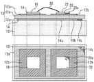
図1は、実施の形態1に係る半導体モジュールの断面図である。この半導体モジュールは絶縁基板12を備えている。絶縁基板12は、絶縁層12aと、絶縁層12aの上面に形成された第1金属パターン12bと、絶縁層12aの下面に形成された第2金属パターン12cとを有している。絶縁層12aの材料は例えばAlN、Al2O3又はSiNである。
図3は、実施の形態2に係る半導体モジュールの断面図である。半導体チップの厚さZ2は0.25mm以上0.35mm以下である。絶縁層12aの厚みZ3は0.8mm以上である。図4は、AlNで形成した絶縁層12aの厚みと、第1金属接合材16、20及び第2金属接合材14に及ぶひずみとの関係を示す図である。図4のAには、参考までに、半導体チップがSiで形成され、絶縁層AlNを0.653mmとしたときの、第1金属接合材16、20と第2金属接合材14の非弾性ひずみ増加分が示されている。
図5は、実施の形態3に係る半導体モジュールの断面図である。絶縁基板12と半導体チップ18はケース50に収容されている。ケース50は、放熱板10に固定されている。ケース50には端子52が固定されている。この端子52にはプリント基板54が固定されている。プリント基板54はケース50の中の絶縁基板12の直上にある。プリント基板54には導電性の材料でランド60が形成されている。このランド60には、制御IC64の端子64aがはんだ62で固定されている。制御IC64は、半導体チップ18を駆動させる駆動回路と、半導体チップ18の保護回路とを集積したICである。制御IC64はケース50の中に収容されている。
図6は、実施の形態4に係る電力変換装置を示す図である。電力変換装置は、実施の形態1〜3のいずれか1つで説明した半導体モジュールを少なくとも1つ有する。すなわち、電力変換装置の少なくとも一箇所は、実施の形態1〜3で説明した厚さの絶縁層12aと、半導体チップが形成される。図6には、半導体チップとして、6つのスイッチング素子と6つの還流ダイオードが設けられ、全体として3相交流インバータ回路を構成する電力変換装置が示されている。インバータ回路に限らず、コンバータ装置、サーボアンプ又は電源ユニットなどを形成してもよい。
Claims (3)
- 絶縁層と、前記絶縁層の上面に形成された第1金属パターンと、前記絶縁層の下面に形成された第2金属パターンとを有する絶縁基板と、
前記第1金属パターンに第1金属接合材で固定され、SiCによって形成された半導体チップと、
前記第2金属パターンに第2金属接合材で固定された放熱板と、を備え、
前記半導体チップの厚みは0.25mm以上0.35mm以下であり、
前記絶縁層の厚みは前記半導体チップの厚みに対し2.66倍以上5倍以下であり、
前記第2金属接合材は、前記半導体チップの直下にある直下部分と、前記直下部分につながり前記半導体チップの直下にない非直下部分とを有し、
前記第1金属接合材に導入されたクラックは、前記非直下部分に導入されたクラックより小規模であることを特徴とする半導体モジュール。 - 前記絶縁層の材料は、AlN、Al2O3又はSiNであることを特徴とする請求項1に記載の半導体モジュール。
- 前記絶縁基板と、前記半導体チップを収容し、前記放熱板に固定されたケースと、
前記半導体チップを駆動させる駆動回路と、前記半導体チップの保護回路とを集積した制御ICと、を備え、
前記制御ICは前記ケースの中に収容されたことを特徴とする請求項1又は2に記載の半導体モジュール。
Priority Applications (4)
| Application Number | Priority Date | Filing Date | Title |
|---|---|---|---|
| JP2016137730A JP6759784B2 (ja) | 2016-07-12 | 2016-07-12 | 半導体モジュール |
| US15/453,966 US10727150B2 (en) | 2016-07-12 | 2017-03-09 | Semiconductor module and power converter |
| DE102017209119.3A DE102017209119B4 (de) | 2016-07-12 | 2017-05-31 | Halbleitermodul und Leistungswandler |
| CN201710565919.9A CN107611111B (zh) | 2016-07-12 | 2017-07-12 | 半导体模块、电力转换装置 |
Applications Claiming Priority (1)
| Application Number | Priority Date | Filing Date | Title |
|---|---|---|---|
| JP2016137730A JP6759784B2 (ja) | 2016-07-12 | 2016-07-12 | 半導体モジュール |
Publications (3)
| Publication Number | Publication Date |
|---|---|
| JP2018010929A JP2018010929A (ja) | 2018-01-18 |
| JP2018010929A5 JP2018010929A5 (ja) | 2019-01-10 |
| JP6759784B2 true JP6759784B2 (ja) | 2020-09-23 |
Family
ID=60783074
Family Applications (1)
| Application Number | Title | Priority Date | Filing Date |
|---|---|---|---|
| JP2016137730A Active JP6759784B2 (ja) | 2016-07-12 | 2016-07-12 | 半導体モジュール |
Country Status (4)
| Country | Link |
|---|---|
| US (1) | US10727150B2 (ja) |
| JP (1) | JP6759784B2 (ja) |
| CN (1) | CN107611111B (ja) |
| DE (1) | DE102017209119B4 (ja) |
Families Citing this family (4)
| Publication number | Priority date | Publication date | Assignee | Title |
|---|---|---|---|---|
| CN114365279A (zh) * | 2019-09-13 | 2022-04-15 | 株式会社电装 | 半导体装置 |
| KR102122210B1 (ko) * | 2019-10-18 | 2020-06-12 | 제엠제코(주) | 방열 기판, 그 제조 방법, 그리고 이를 포함하는 반도체 패키지 |
| JP6822609B1 (ja) * | 2019-10-24 | 2021-01-27 | 三菱電機株式会社 | 熱電変換素子モジュールおよび熱電変換素子モジュールの製造方法 |
| JP7178980B2 (ja) * | 2019-10-30 | 2022-11-28 | 三菱電機株式会社 | 半導体装置 |
Family Cites Families (32)
| Publication number | Priority date | Publication date | Assignee | Title |
|---|---|---|---|---|
| ATE378800T1 (de) | 1999-05-28 | 2007-11-15 | Denki Kagaku Kogyo Kk | Schaltungskeramiksubstrat und sein herstellungsverfahren |
| TW512653B (en) * | 1999-11-26 | 2002-12-01 | Ibiden Co Ltd | Multilayer circuit board and semiconductor device |
| JP2001284513A (ja) * | 2000-03-29 | 2001-10-12 | Mitsubishi Electric Corp | パワー半導体装置 |
| JP2001358263A (ja) * | 2000-06-12 | 2001-12-26 | Hitachi Ltd | 半導体装置およびその回路形成方法 |
| JP3926141B2 (ja) * | 2000-12-27 | 2007-06-06 | 日本特殊陶業株式会社 | 配線基板 |
| US7800222B2 (en) | 2007-11-29 | 2010-09-21 | Infineon Technologies Ag | Semiconductor module with switching components and driver electronics |
| US8304660B2 (en) * | 2008-02-07 | 2012-11-06 | National Taiwan University | Fully reflective and highly thermoconductive electronic module and method of manufacturing the same |
| JP5434914B2 (ja) | 2008-06-12 | 2014-03-05 | 株式会社安川電機 | パワーモジュールおよびその制御方法 |
| EP2518190A1 (en) * | 2009-12-25 | 2012-10-31 | FUJIFILM Corporation | Insulated substrate, process for production of insulated substrate, process for formation of wiring line, wiring substrate, and light-emitting element |
| JP5213884B2 (ja) | 2010-01-27 | 2013-06-19 | 三菱電機株式会社 | 半導体装置モジュール |
| CN103250242B (zh) | 2010-11-25 | 2016-03-30 | 三菱电机株式会社 | 半导体装置以及半导体装置的制造方法 |
| JP5626087B2 (ja) * | 2011-04-13 | 2014-11-19 | 三菱電機株式会社 | 半導体装置 |
| EP2709148A4 (en) * | 2011-05-13 | 2015-07-15 | Fuji Electric Co Ltd | SEMICONDUCTOR COMPONENT AND MANUFACTURING METHOD THEREFOR |
| US8963321B2 (en) * | 2011-09-12 | 2015-02-24 | Infineon Technologies Ag | Semiconductor device including cladded base plate |
| JP5887901B2 (ja) * | 2011-12-14 | 2016-03-16 | 富士電機株式会社 | 半導体装置及び半導体装置の製造方法 |
| US10122293B2 (en) | 2012-01-17 | 2018-11-06 | Infineon Technologies Americas Corp. | Power module package having a multi-phase inverter and power factor correction |
| JP5966504B2 (ja) * | 2012-03-28 | 2016-08-10 | 三菱マテリアル株式会社 | はんだ接合構造、パワーモジュール、ヒートシンク付パワーモジュール用基板、並びに、はんだ接合構造の製造方法、パワーモジュールの製造方法、ヒートシンク付パワーモジュール用基板の製造方法 |
| JP6044097B2 (ja) * | 2012-03-30 | 2016-12-14 | 三菱マテリアル株式会社 | ヒートシンク付パワーモジュール用基板、冷却器付パワーモジュール用基板及びパワーモジュール |
| EP2854174B1 (en) * | 2012-05-22 | 2019-02-20 | Panasonic Intellectual Property Management Co., Ltd. | Semiconductor device and method for manufacturing same |
| JP6147256B2 (ja) * | 2012-07-19 | 2017-06-14 | 三菱電機株式会社 | 電力用半導体モジュール |
| WO2014030659A1 (ja) * | 2012-08-23 | 2014-02-27 | 日産自動車株式会社 | 絶縁基板、多層セラミック絶縁基板、パワー半導体装置と絶縁基板の接合構造体、及びパワー半導体モジュール |
| JP6368646B2 (ja) * | 2012-09-20 | 2018-08-01 | ローム株式会社 | パワーモジュール半導体装置およびインバータ装置、およびパワーモジュール半導体装置の製造方法、および金型 |
| JP6102171B2 (ja) | 2012-10-17 | 2017-03-29 | 富士電機株式会社 | 炭化珪素mos型半導体装置の製造方法 |
| JP2014130875A (ja) | 2012-12-28 | 2014-07-10 | Mitsubishi Electric Corp | 半導体装置およびその製造方法 |
| TWI478479B (zh) * | 2013-01-17 | 2015-03-21 | Delta Electronics Inc | 整合功率模組封裝結構 |
| JP5975911B2 (ja) * | 2013-03-15 | 2016-08-23 | ルネサスエレクトロニクス株式会社 | 半導体装置 |
| JP6265693B2 (ja) | 2013-11-12 | 2018-01-24 | 三菱電機株式会社 | 半導体装置およびその製造方法 |
| JP6129090B2 (ja) | 2014-01-30 | 2017-05-17 | 三菱電機株式会社 | パワーモジュール及びパワーモジュールの製造方法 |
| TWI560829B (en) * | 2014-03-07 | 2016-12-01 | Xintec Inc | Chip package and method thereof |
| JP2015220295A (ja) | 2014-05-15 | 2015-12-07 | 三菱電機株式会社 | パワーモジュール及びその製造方法 |
| JP6233507B2 (ja) * | 2014-05-15 | 2017-11-22 | 富士電機株式会社 | パワー半導体モジュールおよび複合モジュール |
| CN110120375A (zh) * | 2014-05-20 | 2019-08-13 | 三菱电机株式会社 | 功率用半导体装置 |
-
2016
- 2016-07-12 JP JP2016137730A patent/JP6759784B2/ja active Active
-
2017
- 2017-03-09 US US15/453,966 patent/US10727150B2/en active Active
- 2017-05-31 DE DE102017209119.3A patent/DE102017209119B4/de active Active
- 2017-07-12 CN CN201710565919.9A patent/CN107611111B/zh active Active
Also Published As
| Publication number | Publication date |
|---|---|
| US10727150B2 (en) | 2020-07-28 |
| CN107611111A (zh) | 2018-01-19 |
| CN107611111B (zh) | 2021-09-07 |
| DE102017209119B4 (de) | 2024-02-22 |
| DE102017209119A1 (de) | 2018-01-18 |
| US20180019180A1 (en) | 2018-01-18 |
| JP2018010929A (ja) | 2018-01-18 |
Similar Documents
| Publication | Publication Date | Title |
|---|---|---|
| JP5542567B2 (ja) | 半導体装置 | |
| JP7025181B2 (ja) | パワーモジュールおよびその製造方法、グラファイトプレート、および電源装置 | |
| JP6759784B2 (ja) | 半導体モジュール | |
| US20170338189A1 (en) | Insulated circuit board, power module and power unit | |
| JP2013069782A (ja) | 半導体装置 | |
| JP6786416B2 (ja) | 半導体装置 | |
| US9520369B2 (en) | Power module and method of packaging the same | |
| JP2007234690A (ja) | パワー半導体モジュール | |
| US20120306086A1 (en) | Semiconductor device and wiring substrate | |
| JP7040032B2 (ja) | 半導体装置 | |
| JP6988345B2 (ja) | 半導体装置 | |
| JP2010283053A (ja) | 半導体装置及びその製造方法 | |
| JP2013179229A (ja) | パワーモジュール半導体装置 | |
| JP2021190505A (ja) | 半導体装置 | |
| US20130112993A1 (en) | Semiconductor device and wiring substrate | |
| JP7195208B2 (ja) | 半導体装置および半導体装置の製造方法 | |
| JP2013157550A (ja) | パワーモジュール半導体装置およびその製造方法 | |
| JP7163583B2 (ja) | 半導体装置 | |
| KR20210103417A (ko) | 파워모듈 및 그 제조방법 | |
| JP2021141221A (ja) | 半導体モジュール | |
| JP2008306134A (ja) | 半導体モジュール | |
| JP2007227762A (ja) | 半導体装置及びこれを備えた半導体モジュール | |
| JP4375299B2 (ja) | パワー半導体装置 | |
| CN106252307B (zh) | 半导体装置 | |
| US10903138B2 (en) | Semiconductor device and method of manufacturing the same |
Legal Events
| Date | Code | Title | Description |
|---|---|---|---|
| A521 | Request for written amendment filed |
Free format text: JAPANESE INTERMEDIATE CODE: A523 Effective date: 20181119 |
|
| A621 | Written request for application examination |
Free format text: JAPANESE INTERMEDIATE CODE: A621 Effective date: 20181119 |
|
| A977 | Report on retrieval |
Free format text: JAPANESE INTERMEDIATE CODE: A971007 Effective date: 20190807 |
|
| A131 | Notification of reasons for refusal |
Free format text: JAPANESE INTERMEDIATE CODE: A131 Effective date: 20190820 |
|
| A521 | Request for written amendment filed |
Free format text: JAPANESE INTERMEDIATE CODE: A523 Effective date: 20191010 |
|
| A02 | Decision of refusal |
Free format text: JAPANESE INTERMEDIATE CODE: A02 Effective date: 20200310 |
|
| A521 | Request for written amendment filed |
Free format text: JAPANESE INTERMEDIATE CODE: A523 Effective date: 20200522 |
|
| A911 | Transfer to examiner for re-examination before appeal (zenchi) |
Free format text: JAPANESE INTERMEDIATE CODE: A911 Effective date: 20200601 |
|
| TRDD | Decision of grant or rejection written | ||
| A01 | Written decision to grant a patent or to grant a registration (utility model) |
Free format text: JAPANESE INTERMEDIATE CODE: A01 Effective date: 20200804 |
|
| A61 | First payment of annual fees (during grant procedure) |
Free format text: JAPANESE INTERMEDIATE CODE: A61 Effective date: 20200817 |
|
| R150 | Certificate of patent or registration of utility model |
Ref document number: 6759784 Country of ref document: JP Free format text: JAPANESE INTERMEDIATE CODE: R150 |
|
| R250 | Receipt of annual fees |
Free format text: JAPANESE INTERMEDIATE CODE: R250 |
|
| R250 | Receipt of annual fees |
Free format text: JAPANESE INTERMEDIATE CODE: R250 |