JP6759784B2 - Semiconductor module - Google Patents
Semiconductor module Download PDFInfo
- Publication number
- JP6759784B2 JP6759784B2 JP2016137730A JP2016137730A JP6759784B2 JP 6759784 B2 JP6759784 B2 JP 6759784B2 JP 2016137730 A JP2016137730 A JP 2016137730A JP 2016137730 A JP2016137730 A JP 2016137730A JP 6759784 B2 JP6759784 B2 JP 6759784B2
- Authority
- JP
- Japan
- Prior art keywords
- semiconductor chip
- metal bonding
- insulating layer
- semiconductor
- bonding material
- Prior art date
- Legal status (The legal status is an assumption and is not a legal conclusion. Google has not performed a legal analysis and makes no representation as to the accuracy of the status listed.)
- Active
Links
- 239000004065 semiconductor Substances 0.000 title claims description 107
- 229910052751 metal Inorganic materials 0.000 claims description 73
- 239000002184 metal Substances 0.000 claims description 73
- 239000000463 material Substances 0.000 claims description 63
- 239000000758 substrate Substances 0.000 claims description 24
- 229910018072 Al 2 O 3 Inorganic materials 0.000 claims description 2
- 230000017525 heat dissipation Effects 0.000 description 18
- 238000006243 chemical reaction Methods 0.000 description 13
- 229910000679 solder Inorganic materials 0.000 description 9
- 239000000919 ceramic Substances 0.000 description 2
- 230000006866 deterioration Effects 0.000 description 2
- 238000010586 diagram Methods 0.000 description 2
- 238000009413 insulation Methods 0.000 description 2
- 230000000704 physical effect Effects 0.000 description 2
- 239000004020 conductor Substances 0.000 description 1
- PMHQVHHXPFUNSP-UHFFFAOYSA-M copper(1+);methylsulfanylmethane;bromide Chemical compound Br[Cu].CSC PMHQVHHXPFUNSP-UHFFFAOYSA-M 0.000 description 1
- 230000007423 decrease Effects 0.000 description 1
- 230000001771 impaired effect Effects 0.000 description 1
- 238000004519 manufacturing process Methods 0.000 description 1
- 238000005498 polishing Methods 0.000 description 1
- 238000004904 shortening Methods 0.000 description 1
Images


Classifications
-
- H—ELECTRICITY
- H01—ELECTRIC ELEMENTS
- H01L—SEMICONDUCTOR DEVICES NOT COVERED BY CLASS H10
- H01L23/00—Details of semiconductor or other solid state devices
- H01L23/34—Arrangements for cooling, heating, ventilating or temperature compensation ; Temperature sensing arrangements
- H01L23/36—Selection of materials, or shaping, to facilitate cooling or heating, e.g. heatsinks
- H01L23/367—Cooling facilitated by shape of device
- H01L23/3675—Cooling facilitated by shape of device characterised by the shape of the housing
-
- H—ELECTRICITY
- H01—ELECTRIC ELEMENTS
- H01L—SEMICONDUCTOR DEVICES NOT COVERED BY CLASS H10
- H01L23/00—Details of semiconductor or other solid state devices
- H01L23/34—Arrangements for cooling, heating, ventilating or temperature compensation ; Temperature sensing arrangements
- H01L23/36—Selection of materials, or shaping, to facilitate cooling or heating, e.g. heatsinks
- H01L23/373—Cooling facilitated by selection of materials for the device or materials for thermal expansion adaptation, e.g. carbon
- H01L23/3735—Laminates or multilayers, e.g. direct bond copper ceramic substrates
-
- H—ELECTRICITY
- H01—ELECTRIC ELEMENTS
- H01L—SEMICONDUCTOR DEVICES NOT COVERED BY CLASS H10
- H01L23/00—Details of semiconductor or other solid state devices
- H01L23/02—Containers; Seals
- H01L23/04—Containers; Seals characterised by the shape of the container or parts, e.g. caps, walls
-
- H—ELECTRICITY
- H01—ELECTRIC ELEMENTS
- H01L—SEMICONDUCTOR DEVICES NOT COVERED BY CLASS H10
- H01L23/00—Details of semiconductor or other solid state devices
- H01L23/02—Containers; Seals
- H01L23/04—Containers; Seals characterised by the shape of the container or parts, e.g. caps, walls
- H01L23/043—Containers; Seals characterised by the shape of the container or parts, e.g. caps, walls the container being a hollow construction and having a conductive base as a mounting as well as a lead for the semiconductor body
- H01L23/049—Containers; Seals characterised by the shape of the container or parts, e.g. caps, walls the container being a hollow construction and having a conductive base as a mounting as well as a lead for the semiconductor body the other leads being perpendicular to the base
-
- H—ELECTRICITY
- H01—ELECTRIC ELEMENTS
- H01L—SEMICONDUCTOR DEVICES NOT COVERED BY CLASS H10
- H01L23/00—Details of semiconductor or other solid state devices
- H01L23/02—Containers; Seals
- H01L23/04—Containers; Seals characterised by the shape of the container or parts, e.g. caps, walls
- H01L23/053—Containers; Seals characterised by the shape of the container or parts, e.g. caps, walls the container being a hollow construction and having an insulating or insulated base as a mounting for the semiconductor body
-
- H—ELECTRICITY
- H01—ELECTRIC ELEMENTS
- H01L—SEMICONDUCTOR DEVICES NOT COVERED BY CLASS H10
- H01L23/00—Details of semiconductor or other solid state devices
- H01L23/34—Arrangements for cooling, heating, ventilating or temperature compensation ; Temperature sensing arrangements
- H01L23/36—Selection of materials, or shaping, to facilitate cooling or heating, e.g. heatsinks
-
- H—ELECTRICITY
- H01—ELECTRIC ELEMENTS
- H01L—SEMICONDUCTOR DEVICES NOT COVERED BY CLASS H10
- H01L24/00—Arrangements for connecting or disconnecting semiconductor or solid-state bodies; Methods or apparatus related thereto
-
- H—ELECTRICITY
- H01—ELECTRIC ELEMENTS
- H01L—SEMICONDUCTOR DEVICES NOT COVERED BY CLASS H10
- H01L24/00—Arrangements for connecting or disconnecting semiconductor or solid-state bodies; Methods or apparatus related thereto
- H01L24/01—Means for bonding being attached to, or being formed on, the surface to be connected, e.g. chip-to-package, die-attach, "first-level" interconnects; Manufacturing methods related thereto
- H01L24/26—Layer connectors, e.g. plate connectors, solder or adhesive layers; Manufacturing methods related thereto
- H01L24/31—Structure, shape, material or disposition of the layer connectors after the connecting process
- H01L24/32—Structure, shape, material or disposition of the layer connectors after the connecting process of an individual layer connector
-
- H—ELECTRICITY
- H01—ELECTRIC ELEMENTS
- H01L—SEMICONDUCTOR DEVICES NOT COVERED BY CLASS H10
- H01L25/00—Assemblies consisting of a plurality of individual semiconductor or other solid state devices ; Multistep manufacturing processes thereof
- H01L25/03—Assemblies consisting of a plurality of individual semiconductor or other solid state devices ; Multistep manufacturing processes thereof all the devices being of a type provided for in the same subgroup of groups H01L27/00 - H01L33/00, or in a single subclass of H10K, H10N, e.g. assemblies of rectifier diodes
- H01L25/04—Assemblies consisting of a plurality of individual semiconductor or other solid state devices ; Multistep manufacturing processes thereof all the devices being of a type provided for in the same subgroup of groups H01L27/00 - H01L33/00, or in a single subclass of H10K, H10N, e.g. assemblies of rectifier diodes the devices not having separate containers
- H01L25/07—Assemblies consisting of a plurality of individual semiconductor or other solid state devices ; Multistep manufacturing processes thereof all the devices being of a type provided for in the same subgroup of groups H01L27/00 - H01L33/00, or in a single subclass of H10K, H10N, e.g. assemblies of rectifier diodes the devices not having separate containers the devices being of a type provided for in group H01L29/00
- H01L25/071—Assemblies consisting of a plurality of individual semiconductor or other solid state devices ; Multistep manufacturing processes thereof all the devices being of a type provided for in the same subgroup of groups H01L27/00 - H01L33/00, or in a single subclass of H10K, H10N, e.g. assemblies of rectifier diodes the devices not having separate containers the devices being of a type provided for in group H01L29/00 the devices being arranged next and on each other, i.e. mixed assemblies
-
- H—ELECTRICITY
- H01—ELECTRIC ELEMENTS
- H01L—SEMICONDUCTOR DEVICES NOT COVERED BY CLASS H10
- H01L25/00—Assemblies consisting of a plurality of individual semiconductor or other solid state devices ; Multistep manufacturing processes thereof
- H01L25/03—Assemblies consisting of a plurality of individual semiconductor or other solid state devices ; Multistep manufacturing processes thereof all the devices being of a type provided for in the same subgroup of groups H01L27/00 - H01L33/00, or in a single subclass of H10K, H10N, e.g. assemblies of rectifier diodes
- H01L25/04—Assemblies consisting of a plurality of individual semiconductor or other solid state devices ; Multistep manufacturing processes thereof all the devices being of a type provided for in the same subgroup of groups H01L27/00 - H01L33/00, or in a single subclass of H10K, H10N, e.g. assemblies of rectifier diodes the devices not having separate containers
- H01L25/07—Assemblies consisting of a plurality of individual semiconductor or other solid state devices ; Multistep manufacturing processes thereof all the devices being of a type provided for in the same subgroup of groups H01L27/00 - H01L33/00, or in a single subclass of H10K, H10N, e.g. assemblies of rectifier diodes the devices not having separate containers the devices being of a type provided for in group H01L29/00
- H01L25/072—Assemblies consisting of a plurality of individual semiconductor or other solid state devices ; Multistep manufacturing processes thereof all the devices being of a type provided for in the same subgroup of groups H01L27/00 - H01L33/00, or in a single subclass of H10K, H10N, e.g. assemblies of rectifier diodes the devices not having separate containers the devices being of a type provided for in group H01L29/00 the devices being arranged next to each other
-
- H—ELECTRICITY
- H01—ELECTRIC ELEMENTS
- H01L—SEMICONDUCTOR DEVICES NOT COVERED BY CLASS H10
- H01L25/00—Assemblies consisting of a plurality of individual semiconductor or other solid state devices ; Multistep manufacturing processes thereof
- H01L25/18—Assemblies consisting of a plurality of individual semiconductor or other solid state devices ; Multistep manufacturing processes thereof the devices being of types provided for in two or more different subgroups of the same main group of groups H01L27/00 - H01L33/00, or in a single subclass of H10K, H10N
-
- H—ELECTRICITY
- H02—GENERATION; CONVERSION OR DISTRIBUTION OF ELECTRIC POWER
- H02M—APPARATUS FOR CONVERSION BETWEEN AC AND AC, BETWEEN AC AND DC, OR BETWEEN DC AND DC, AND FOR USE WITH MAINS OR SIMILAR POWER SUPPLY SYSTEMS; CONVERSION OF DC OR AC INPUT POWER INTO SURGE OUTPUT POWER; CONTROL OR REGULATION THEREOF
- H02M7/00—Conversion of ac power input into dc power output; Conversion of dc power input into ac power output
- H02M7/42—Conversion of dc power input into ac power output without possibility of reversal
- H02M7/44—Conversion of dc power input into ac power output without possibility of reversal by static converters
- H02M7/48—Conversion of dc power input into ac power output without possibility of reversal by static converters using discharge tubes with control electrode or semiconductor devices with control electrode
- H02M7/53—Conversion of dc power input into ac power output without possibility of reversal by static converters using discharge tubes with control electrode or semiconductor devices with control electrode using devices of a triode or transistor type requiring continuous application of a control signal
- H02M7/537—Conversion of dc power input into ac power output without possibility of reversal by static converters using discharge tubes with control electrode or semiconductor devices with control electrode using devices of a triode or transistor type requiring continuous application of a control signal using semiconductor devices only, e.g. single switched pulse inverters
-
- H—ELECTRICITY
- H01—ELECTRIC ELEMENTS
- H01L—SEMICONDUCTOR DEVICES NOT COVERED BY CLASS H10
- H01L2224/00—Indexing scheme for arrangements for connecting or disconnecting semiconductor or solid-state bodies and methods related thereto as covered by H01L24/00
- H01L2224/01—Means for bonding being attached to, or being formed on, the surface to be connected, e.g. chip-to-package, die-attach, "first-level" interconnects; Manufacturing methods related thereto
- H01L2224/10—Bump connectors; Manufacturing methods related thereto
- H01L2224/15—Structure, shape, material or disposition of the bump connectors after the connecting process
- H01L2224/16—Structure, shape, material or disposition of the bump connectors after the connecting process of an individual bump connector
- H01L2224/161—Disposition
- H01L2224/16151—Disposition the bump connector connecting between a semiconductor or solid-state body and an item not being a semiconductor or solid-state body, e.g. chip-to-substrate, chip-to-passive
- H01L2224/16221—Disposition the bump connector connecting between a semiconductor or solid-state body and an item not being a semiconductor or solid-state body, e.g. chip-to-substrate, chip-to-passive the body and the item being stacked
- H01L2224/16225—Disposition the bump connector connecting between a semiconductor or solid-state body and an item not being a semiconductor or solid-state body, e.g. chip-to-substrate, chip-to-passive the body and the item being stacked the item being non-metallic, e.g. insulating substrate with or without metallisation
-
- H—ELECTRICITY
- H01—ELECTRIC ELEMENTS
- H01L—SEMICONDUCTOR DEVICES NOT COVERED BY CLASS H10
- H01L2224/00—Indexing scheme for arrangements for connecting or disconnecting semiconductor or solid-state bodies and methods related thereto as covered by H01L24/00
- H01L2224/01—Means for bonding being attached to, or being formed on, the surface to be connected, e.g. chip-to-package, die-attach, "first-level" interconnects; Manufacturing methods related thereto
- H01L2224/26—Layer connectors, e.g. plate connectors, solder or adhesive layers; Manufacturing methods related thereto
- H01L2224/28—Structure, shape, material or disposition of the layer connectors prior to the connecting process
- H01L2224/29—Structure, shape, material or disposition of the layer connectors prior to the connecting process of an individual layer connector
- H01L2224/29001—Core members of the layer connector
- H01L2224/29099—Material
- H01L2224/291—Material with a principal constituent of the material being a metal or a metalloid, e.g. boron [B], silicon [Si], germanium [Ge], arsenic [As], antimony [Sb], tellurium [Te] and polonium [Po], and alloys thereof
-
- H—ELECTRICITY
- H01—ELECTRIC ELEMENTS
- H01L—SEMICONDUCTOR DEVICES NOT COVERED BY CLASS H10
- H01L2224/00—Indexing scheme for arrangements for connecting or disconnecting semiconductor or solid-state bodies and methods related thereto as covered by H01L24/00
- H01L2224/01—Means for bonding being attached to, or being formed on, the surface to be connected, e.g. chip-to-package, die-attach, "first-level" interconnects; Manufacturing methods related thereto
- H01L2224/26—Layer connectors, e.g. plate connectors, solder or adhesive layers; Manufacturing methods related thereto
- H01L2224/31—Structure, shape, material or disposition of the layer connectors after the connecting process
- H01L2224/32—Structure, shape, material or disposition of the layer connectors after the connecting process of an individual layer connector
- H01L2224/321—Disposition
- H01L2224/32151—Disposition the layer connector connecting between a semiconductor or solid-state body and an item not being a semiconductor or solid-state body, e.g. chip-to-substrate, chip-to-passive
- H01L2224/32221—Disposition the layer connector connecting between a semiconductor or solid-state body and an item not being a semiconductor or solid-state body, e.g. chip-to-substrate, chip-to-passive the body and the item being stacked
- H01L2224/32245—Disposition the layer connector connecting between a semiconductor or solid-state body and an item not being a semiconductor or solid-state body, e.g. chip-to-substrate, chip-to-passive the body and the item being stacked the item being metallic
-
- H—ELECTRICITY
- H01—ELECTRIC ELEMENTS
- H01L—SEMICONDUCTOR DEVICES NOT COVERED BY CLASS H10
- H01L2224/00—Indexing scheme for arrangements for connecting or disconnecting semiconductor or solid-state bodies and methods related thereto as covered by H01L24/00
- H01L2224/01—Means for bonding being attached to, or being formed on, the surface to be connected, e.g. chip-to-package, die-attach, "first-level" interconnects; Manufacturing methods related thereto
- H01L2224/42—Wire connectors; Manufacturing methods related thereto
- H01L2224/47—Structure, shape, material or disposition of the wire connectors after the connecting process
- H01L2224/48—Structure, shape, material or disposition of the wire connectors after the connecting process of an individual wire connector
- H01L2224/4805—Shape
- H01L2224/4809—Loop shape
- H01L2224/48091—Arched
-
- H—ELECTRICITY
- H01—ELECTRIC ELEMENTS
- H01L—SEMICONDUCTOR DEVICES NOT COVERED BY CLASS H10
- H01L2224/00—Indexing scheme for arrangements for connecting or disconnecting semiconductor or solid-state bodies and methods related thereto as covered by H01L24/00
- H01L2224/01—Means for bonding being attached to, or being formed on, the surface to be connected, e.g. chip-to-package, die-attach, "first-level" interconnects; Manufacturing methods related thereto
- H01L2224/42—Wire connectors; Manufacturing methods related thereto
- H01L2224/47—Structure, shape, material or disposition of the wire connectors after the connecting process
- H01L2224/48—Structure, shape, material or disposition of the wire connectors after the connecting process of an individual wire connector
- H01L2224/481—Disposition
- H01L2224/48105—Connecting bonding areas at different heights
- H01L2224/48106—Connecting bonding areas at different heights the connector being orthogonal to a side surface of the semiconductor or solid-state body, e.g. parallel layout
-
- H—ELECTRICITY
- H01—ELECTRIC ELEMENTS
- H01L—SEMICONDUCTOR DEVICES NOT COVERED BY CLASS H10
- H01L2224/00—Indexing scheme for arrangements for connecting or disconnecting semiconductor or solid-state bodies and methods related thereto as covered by H01L24/00
- H01L2224/01—Means for bonding being attached to, or being formed on, the surface to be connected, e.g. chip-to-package, die-attach, "first-level" interconnects; Manufacturing methods related thereto
- H01L2224/42—Wire connectors; Manufacturing methods related thereto
- H01L2224/47—Structure, shape, material or disposition of the wire connectors after the connecting process
- H01L2224/48—Structure, shape, material or disposition of the wire connectors after the connecting process of an individual wire connector
- H01L2224/481—Disposition
- H01L2224/48135—Connecting between different semiconductor or solid-state bodies, i.e. chip-to-chip
- H01L2224/48137—Connecting between different semiconductor or solid-state bodies, i.e. chip-to-chip the bodies being arranged next to each other, e.g. on a common substrate
-
- H—ELECTRICITY
- H01—ELECTRIC ELEMENTS
- H01L—SEMICONDUCTOR DEVICES NOT COVERED BY CLASS H10
- H01L2224/00—Indexing scheme for arrangements for connecting or disconnecting semiconductor or solid-state bodies and methods related thereto as covered by H01L24/00
- H01L2224/01—Means for bonding being attached to, or being formed on, the surface to be connected, e.g. chip-to-package, die-attach, "first-level" interconnects; Manufacturing methods related thereto
- H01L2224/42—Wire connectors; Manufacturing methods related thereto
- H01L2224/47—Structure, shape, material or disposition of the wire connectors after the connecting process
- H01L2224/48—Structure, shape, material or disposition of the wire connectors after the connecting process of an individual wire connector
- H01L2224/481—Disposition
- H01L2224/48151—Connecting between a semiconductor or solid-state body and an item not being a semiconductor or solid-state body, e.g. chip-to-substrate, chip-to-passive
- H01L2224/48153—Connecting between a semiconductor or solid-state body and an item not being a semiconductor or solid-state body, e.g. chip-to-substrate, chip-to-passive the body and the item being arranged next to each other, e.g. on a common substrate
- H01L2224/48175—Connecting between a semiconductor or solid-state body and an item not being a semiconductor or solid-state body, e.g. chip-to-substrate, chip-to-passive the body and the item being arranged next to each other, e.g. on a common substrate the item being metallic
-
- H—ELECTRICITY
- H01—ELECTRIC ELEMENTS
- H01L—SEMICONDUCTOR DEVICES NOT COVERED BY CLASS H10
- H01L2224/00—Indexing scheme for arrangements for connecting or disconnecting semiconductor or solid-state bodies and methods related thereto as covered by H01L24/00
- H01L2224/01—Means for bonding being attached to, or being formed on, the surface to be connected, e.g. chip-to-package, die-attach, "first-level" interconnects; Manufacturing methods related thereto
- H01L2224/42—Wire connectors; Manufacturing methods related thereto
- H01L2224/47—Structure, shape, material or disposition of the wire connectors after the connecting process
- H01L2224/48—Structure, shape, material or disposition of the wire connectors after the connecting process of an individual wire connector
- H01L2224/481—Disposition
- H01L2224/48151—Connecting between a semiconductor or solid-state body and an item not being a semiconductor or solid-state body, e.g. chip-to-substrate, chip-to-passive
- H01L2224/48221—Connecting between a semiconductor or solid-state body and an item not being a semiconductor or solid-state body, e.g. chip-to-substrate, chip-to-passive the body and the item being stacked
- H01L2224/48245—Connecting between a semiconductor or solid-state body and an item not being a semiconductor or solid-state body, e.g. chip-to-substrate, chip-to-passive the body and the item being stacked the item being metallic
-
- H—ELECTRICITY
- H01—ELECTRIC ELEMENTS
- H01L—SEMICONDUCTOR DEVICES NOT COVERED BY CLASS H10
- H01L2224/00—Indexing scheme for arrangements for connecting or disconnecting semiconductor or solid-state bodies and methods related thereto as covered by H01L24/00
- H01L2224/73—Means for bonding being of different types provided for in two or more of groups H01L2224/10, H01L2224/18, H01L2224/26, H01L2224/34, H01L2224/42, H01L2224/50, H01L2224/63, H01L2224/71
- H01L2224/732—Location after the connecting process
- H01L2224/73251—Location after the connecting process on different surfaces
- H01L2224/73265—Layer and wire connectors
-
- H—ELECTRICITY
- H01—ELECTRIC ELEMENTS
- H01L—SEMICONDUCTOR DEVICES NOT COVERED BY CLASS H10
- H01L24/00—Arrangements for connecting or disconnecting semiconductor or solid-state bodies; Methods or apparatus related thereto
- H01L24/01—Means for bonding being attached to, or being formed on, the surface to be connected, e.g. chip-to-package, die-attach, "first-level" interconnects; Manufacturing methods related thereto
- H01L24/42—Wire connectors; Manufacturing methods related thereto
- H01L24/47—Structure, shape, material or disposition of the wire connectors after the connecting process
- H01L24/48—Structure, shape, material or disposition of the wire connectors after the connecting process of an individual wire connector
-
- H—ELECTRICITY
- H01—ELECTRIC ELEMENTS
- H01L—SEMICONDUCTOR DEVICES NOT COVERED BY CLASS H10
- H01L24/00—Arrangements for connecting or disconnecting semiconductor or solid-state bodies; Methods or apparatus related thereto
- H01L24/01—Means for bonding being attached to, or being formed on, the surface to be connected, e.g. chip-to-package, die-attach, "first-level" interconnects; Manufacturing methods related thereto
- H01L24/42—Wire connectors; Manufacturing methods related thereto
- H01L24/47—Structure, shape, material or disposition of the wire connectors after the connecting process
- H01L24/49—Structure, shape, material or disposition of the wire connectors after the connecting process of a plurality of wire connectors
-
- H—ELECTRICITY
- H01—ELECTRIC ELEMENTS
- H01L—SEMICONDUCTOR DEVICES NOT COVERED BY CLASS H10
- H01L2924/00—Indexing scheme for arrangements or methods for connecting or disconnecting semiconductor or solid-state bodies as covered by H01L24/00
- H01L2924/049—Nitrides composed of metals from groups of the periodic table
- H01L2924/0503—13th Group
- H01L2924/05032—AlN
-
- H—ELECTRICITY
- H01—ELECTRIC ELEMENTS
- H01L—SEMICONDUCTOR DEVICES NOT COVERED BY CLASS H10
- H01L2924/00—Indexing scheme for arrangements or methods for connecting or disconnecting semiconductor or solid-state bodies as covered by H01L24/00
- H01L2924/049—Nitrides composed of metals from groups of the periodic table
- H01L2924/0504—14th Group
- H01L2924/05042—Si3N4
-
- H—ELECTRICITY
- H01—ELECTRIC ELEMENTS
- H01L—SEMICONDUCTOR DEVICES NOT COVERED BY CLASS H10
- H01L2924/00—Indexing scheme for arrangements or methods for connecting or disconnecting semiconductor or solid-state bodies as covered by H01L24/00
- H01L2924/053—Oxides composed of metals from groups of the periodic table
- H01L2924/0543—13th Group
- H01L2924/05432—Al2O3
-
- H—ELECTRICITY
- H01—ELECTRIC ELEMENTS
- H01L—SEMICONDUCTOR DEVICES NOT COVERED BY CLASS H10
- H01L2924/00—Indexing scheme for arrangements or methods for connecting or disconnecting semiconductor or solid-state bodies as covered by H01L24/00
- H01L2924/10—Details of semiconductor or other solid state devices to be connected
- H01L2924/102—Material of the semiconductor or solid state bodies
- H01L2924/1025—Semiconducting materials
- H01L2924/1026—Compound semiconductors
- H01L2924/1027—IV
- H01L2924/10272—Silicon Carbide [SiC]
-
- H—ELECTRICITY
- H01—ELECTRIC ELEMENTS
- H01L—SEMICONDUCTOR DEVICES NOT COVERED BY CLASS H10
- H01L2924/00—Indexing scheme for arrangements or methods for connecting or disconnecting semiconductor or solid-state bodies as covered by H01L24/00
- H01L2924/10—Details of semiconductor or other solid state devices to be connected
- H01L2924/11—Device type
- H01L2924/12—Passive devices, e.g. 2 terminal devices
- H01L2924/1203—Rectifying Diode
-
- H—ELECTRICITY
- H01—ELECTRIC ELEMENTS
- H01L—SEMICONDUCTOR DEVICES NOT COVERED BY CLASS H10
- H01L2924/00—Indexing scheme for arrangements or methods for connecting or disconnecting semiconductor or solid-state bodies as covered by H01L24/00
- H01L2924/10—Details of semiconductor or other solid state devices to be connected
- H01L2924/11—Device type
- H01L2924/13—Discrete devices, e.g. 3 terminal devices
- H01L2924/1304—Transistor
- H01L2924/1305—Bipolar Junction Transistor [BJT]
- H01L2924/13055—Insulated gate bipolar transistor [IGBT]
-
- H—ELECTRICITY
- H01—ELECTRIC ELEMENTS
- H01L—SEMICONDUCTOR DEVICES NOT COVERED BY CLASS H10
- H01L2924/00—Indexing scheme for arrangements or methods for connecting or disconnecting semiconductor or solid-state bodies as covered by H01L24/00
- H01L2924/10—Details of semiconductor or other solid state devices to be connected
- H01L2924/11—Device type
- H01L2924/13—Discrete devices, e.g. 3 terminal devices
- H01L2924/1304—Transistor
- H01L2924/1306—Field-effect transistor [FET]
- H01L2924/13091—Metal-Oxide-Semiconductor Field-Effect Transistor [MOSFET]
-
- H—ELECTRICITY
- H01—ELECTRIC ELEMENTS
- H01L—SEMICONDUCTOR DEVICES NOT COVERED BY CLASS H10
- H01L2924/00—Indexing scheme for arrangements or methods for connecting or disconnecting semiconductor or solid-state bodies as covered by H01L24/00
- H01L2924/10—Details of semiconductor or other solid state devices to be connected
- H01L2924/11—Device type
- H01L2924/14—Integrated circuits
- H01L2924/141—Analog devices
- H01L2924/1425—Converter
-
- H—ELECTRICITY
- H01—ELECTRIC ELEMENTS
- H01L—SEMICONDUCTOR DEVICES NOT COVERED BY CLASS H10
- H01L2924/00—Indexing scheme for arrangements or methods for connecting or disconnecting semiconductor or solid-state bodies as covered by H01L24/00
- H01L2924/10—Details of semiconductor or other solid state devices to be connected
- H01L2924/11—Device type
- H01L2924/14—Integrated circuits
- H01L2924/141—Analog devices
- H01L2924/1426—Driver
-
- H—ELECTRICITY
- H01—ELECTRIC ELEMENTS
- H01L—SEMICONDUCTOR DEVICES NOT COVERED BY CLASS H10
- H01L2924/00—Indexing scheme for arrangements or methods for connecting or disconnecting semiconductor or solid-state bodies as covered by H01L24/00
- H01L2924/30—Technical effects
- H01L2924/35—Mechanical effects
- H01L2924/351—Thermal stress
- H01L2924/3512—Cracking
Landscapes
- Engineering & Computer Science (AREA)
- Power Engineering (AREA)
- Microelectronics & Electronic Packaging (AREA)
- Computer Hardware Design (AREA)
- Physics & Mathematics (AREA)
- Condensed Matter Physics & Semiconductors (AREA)
- General Physics & Mathematics (AREA)
- Chemical & Material Sciences (AREA)
- Materials Engineering (AREA)
- Ceramic Engineering (AREA)
- Cooling Or The Like Of Semiconductors Or Solid State Devices (AREA)
- Inverter Devices (AREA)
Description
本発明は、例えば大電流のスイッチングなどに用いられる半導体モジュール、及びその半導体モジュールを用いた電力変換装置に関する。 The present invention relates to a semiconductor module used for switching a large current, for example, and a power conversion device using the semiconductor module.
特許文献1には、セラミック板と、セラミック板の上面と下面に形成された電極とを有する絶縁基板が開示されている。そして、一方の電極には金属接合材でベース板が固定され、他方の電極には金属接合材で半導体素子が固定されている。 Patent Document 1 discloses an insulating substrate having a ceramic plate and electrodes formed on the upper surface and the lower surface of the ceramic plate. The base plate is fixed to one electrode with a metal bonding material, and the semiconductor element is fixed to the other electrode with a metal bonding material.
電力制御用の半導体モジュールは、IGBT、MOSFET及びFWDi等の半導体チップを搭載している。このような半導体モジュールはパワーモジュールと呼ばれている。パワーモジュールは、放熱板にはんだ接合された絶縁基板と、絶縁基板の金属パターンにはんだ接合された半導体チップを備える。 The semiconductor module for power control is equipped with a semiconductor chip such as an IGBT, MOSFET, and FWDi. Such a semiconductor module is called a power module. The power module includes an insulating substrate solder-bonded to the heat dissipation plate and a semiconductor chip solder-bonded to the metal pattern of the insulating substrate.
パワーモジュールの応用製品であるインバータ機器には低損失化と小型化が求められているため、半導体モジュールにも低損失化と小型化が求められている。低損失化は、搭載する半導体チップを薄くしたり、半導体チップ構造を最適化したりすることにより実現される。小型化はパッケージ構造の最適化により実現される。しかしながら、半導体モジュールを小型化すると、半導体モジュール内で半導体チップが密集し、放熱面積も小さくなるので、放熱性の悪化が懸念される。この放熱性の悪化を回避するために絶縁基板の絶縁層を薄くすることが考えられる。 Since inverter devices, which are application products of power modules, are required to have low loss and miniaturization, semiconductor modules are also required to have low loss and miniaturization. Low loss is realized by thinning the mounted semiconductor chip and optimizing the semiconductor chip structure. Miniaturization is realized by optimizing the package structure. However, when the semiconductor module is miniaturized, the semiconductor chips are densely packed in the semiconductor module and the heat dissipation area is also reduced, so that there is a concern that the heat dissipation property may be deteriorated. In order to avoid this deterioration of heat dissipation, it is conceivable to thin the insulating layer of the insulating substrate.
このように、半導体モジュールの低損失化のために半導体チップを薄くし、放熱性改善のために絶縁基板の絶縁層を薄くする、というのが最近の傾向である。 As described above, the recent trend is to make the semiconductor chip thinner in order to reduce the loss of the semiconductor module, and to make the insulating layer of the insulating substrate thinner in order to improve heat dissipation.
半導体チップと絶縁基板を接合する第1はんだと、絶縁基板と放熱板を接合する第2はんだは、半導体モジュール使用時に半導体チップの接合温度とケース温度に大きな温度変化が生じる動作パターンにおいて、半導体チップ、絶縁基板、及び放熱板の線膨張係数差によって熱疲労を起こす。熱疲労により第1はんだと第2はんだにクラックが生じると、半導体チップの放熱性が悪化し信頼性の寿命が低下する問題があった。 The first solder that joins the semiconductor chip and the insulating substrate and the second solder that joins the insulating substrate and the heat dissipation plate are the semiconductor chips in an operation pattern in which the bonding temperature and the case temperature of the semiconductor chip change significantly when the semiconductor module is used. Thermal fatigue is caused by the difference in linear expansion coefficient between the insulating substrate and the heat radiating plate. When cracks occur in the first solder and the second solder due to thermal fatigue, there is a problem that the heat dissipation of the semiconductor chip deteriorates and the reliability life is shortened.
特にSiCのようなSiと比較して固い物性値を持つ材料で半導体チップを形成すると、温度変化時に第1はんだに大きな応力歪が生じる。絶縁層を薄くすると第1はんだにさらに大きな応力歪がかかり、半導体モジュールの寿命を短くする問題があった。 In particular, when a semiconductor chip is formed of a material having a hard physical property value as compared with Si such as SiC, a large stress strain is generated in the first solder when the temperature changes. When the insulating layer is made thin, a larger stress strain is applied to the first solder, which has a problem of shortening the life of the semiconductor module.
半導体チップの厚みを薄くすることによって第1はんだにかかる応力歪を低減することが考えられる。しかし、SiCはSiに比べて固い材質であるため、ウエハを薄くするために用いる研磨治具の摩耗が激しく量産効率が悪化する。 It is conceivable to reduce the stress-strain applied to the first solder by reducing the thickness of the semiconductor chip. However, since SiC is a harder material than Si, the polishing jig used for thinning the wafer is heavily worn and the mass production efficiency is deteriorated.
本発明は、上述のような課題を解決するためになされたもので、半導体チップの放熱性を高く保つことができる半導体モジュールと電力変換装置を提供することを目的とする。 The present invention has been made to solve the above-mentioned problems, and an object of the present invention is to provide a semiconductor module and a power conversion device capable of maintaining high heat dissipation of a semiconductor chip.
本願の発明に係る半導体モジュールは、絶縁層と、該絶縁層の上面に形成された第1金属パターンと、該絶縁層の下面に形成された第2金属パターンとを有する絶縁基板と、該第1金属パターンに第1金属接合材で固定され、SiCによって形成された半導体チップと、該第2金属パターンに第2金属接合材で固定された放熱板と、を備え、該半導体チップの厚みは0.25mm以上0.35mm以下であり、該絶縁層の厚みは該半導体チップの厚みに対し2.66倍以上5倍以下であり、該第2金属接合材は、該半導体チップの直下にある直下部分と、該直下部分につながり該半導体チップの直下にない非直下部分とを有し、該第1金属接合材に導入されたクラックは、該非直下部分に導入されたクラックより小規模であることを特徴とする。
The semiconductor module according to the present invention includes an insulating substrate having an insulating layer, a first metal pattern formed on the upper surface of the insulating layer, and a second metal pattern formed on the lower surface of the insulating layer, and the first metal pattern. A semiconductor chip fixed to a metal pattern with a first metal bonding material and formed of SiC, and a heat radiating plate fixed to the second metal pattern with a second metal bonding material are provided, and the thickness of the semiconductor chip is The thickness of the insulating layer is 0.25 mm or more and 0.35 mm or less, the thickness of the insulating layer is 2.66 times or more and 5 times or less with respect to the thickness of the semiconductor chip, and the second metal bonding material is directly below the semiconductor chip. and just below the portion, and a non-directly below the portion not in the right under the ties the semiconductor chip to the straight lower portion, cracks introduced into the first metal bonding material, on a small scale from cracks introduced into the non-directly under part characterized in that there.
本発明によれば、半導体チップの直下に形成される第1金属接合材のクラックを抑制し、SiC半導体チップを用いたときに大きく形成される基板である絶縁基板の下の第2金属接合材のクラックを許容することで、半導体チップの放熱性を高く保つことができる。 According to the present invention, the second metal bonding material under the insulating substrate, which is a substrate that is largely formed when a SiC semiconductor chip is used, suppresses cracks in the first metal bonding material formed directly under the semiconductor chip. By allowing cracks in the semiconductor chip, the heat dissipation of the semiconductor chip can be kept high.
本発明の実施の形態に係る半導体モジュールと電力変換装置について図面を参照して説明する。同じ又は対応する構成要素には同じ符号を付し、説明の繰り返しを省略する場合がある。 The semiconductor module and the power conversion device according to the embodiment of the present invention will be described with reference to the drawings. The same or corresponding components may be designated by the same reference numerals and the description may be omitted.
実施の形態1.
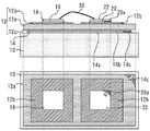
図1は、実施の形態1に係る半導体モジュールの断面図である。この半導体モジュールは絶縁基板12を備えている。絶縁基板12は、絶縁層12aと、絶縁層12aの上面に形成された第1金属パターン12bと、絶縁層12aの下面に形成された第2金属パターン12cとを有している。絶縁層12aの材料は例えばAlN、Al2O3又はSiNである。
Embodiment 1.
FIG. 1 is a cross-sectional view of the semiconductor module according to the first embodiment. This semiconductor module includes an
第1金属パターン12bには第1金属接合材16、20で半導体チップ18、22が固定されている。半導体チップ18、22はSiCによって形成されている。半導体チップ18は例えばIGBT(Insulated Gate Bipolar Transistor)であり、半導体チップ22は例えば還流ダイオードである。SiCによって形成された半導体チップ又はウエハの厚みは0.25mm〜0.35mmとすることが一般的である。例えば、特開2014−82361号公報の明細書段落0005にはn型SiCウエハの厚さが350μmであることが開示されている。本発明の実施の形態1に係る半導体モジュールの半導体チップ18、22の厚みZ2は0.25mm以上0.35mm以下とした。
The
第2金属パターン12cには第2金属接合材14によって放熱板10が固定されている。放熱板10は例えば金属などの放熱性の高い材料で形成する。第1金属接合材16、20と第2金属接合材14は例えばはんだである。第2金属接合材14は、半導体チップ18、22の直下にある直下部分14aと、直下部分14aにつながり半導体チップ18、22の直下にない非直下部分14bとを有している。第2金属接合材14が形成される面積は、第1金属接合材16、20が形成される面積より大きい。
The
ところで、絶縁層12aと半導体チップ18、22の物性値及び線膨張係数の関係から、絶縁層12aの厚みを厚くすると、半導体チップ18、22下の第1金属接合材16、20の歪みが低減され、絶縁基板12下の第2金属接合材14の歪みが増加する。このような関係は、絶縁層12aを窒化アルミで形成し、半導体チップ18、22をSiCで形成した場合だけでなく、一般的に成立する関係である。
By the way, from the relationship between the physical properties of the
熱サイクルによって半導体モジュールの各部が膨張と収縮を繰り返すと、第1金属接合材16、20の端部にクラックが形成され、第2金属接合材14の端部にクラックが形成される。図1には第1金属接合材20に形成されたクラック20aと、第2金属接合材14に形成されたクラック14cが示されている。
When each part of the semiconductor module repeatedly expands and contracts due to the thermal cycle, cracks are formed at the ends of the first
図2には、半導体モジュールの断面図と平面図が示されている。図2において、第2金属接合材14に形成されたクラック14cと、第1金属接合材20に形成されたクラック20aを説明の便宜のために表示する。第1金属接合材20のクラック20aは半導体チップ22の放熱性の悪化に直結する。他方、第2金属接合材14のクラック14cについては、非直下部分14bに形成されたものであるから、半導体チップ22の放熱性への影響は小さい。
FIG. 2 shows a cross-sectional view and a plan view of the semiconductor module. In FIG. 2, the
そして、クラック20a、14cの規模は、上述のとおり絶縁層12aの厚さで調整できる。本発明の実施の形態1では、絶縁層12aの厚みZ1は半導体チップ18、22の厚みZ2に対し2.66倍以上5倍以下とした。すなわち、絶縁層12aを厚くして、半導体チップ18、22下の第1金属接合材16、20のクラックを低減し、絶縁基板12下の第2金属接合材14のクラックが増加するようにした。
The scale of the
つまり、半導体チップ18、20の放熱性を大きく悪化させる第1金属接合材16、20のクラックを抑制しつつ、半導体チップ18、20の放熱性への寄与が小さい第2金属接合材14の非直下部分14bにクラックを生成させる。これにより、半導体チップの放熱性を高く保つことができる。半導体チップ18、20の材料をSiCのような固い材料とした場合には第1金属接合材16、20に特にクラックが生じやすいが、上記のようにクラックの発生しやすさを調整することで、第1金属接合材16、20の熱疲労に起因するクラックを抑制又は小規模にとどめることができる。
That is, the second
このように、本発明の実施の形態1に係る半導体モジュールでは、第1金属接合材16、20に導入されたクラックは、第2金属接合材14に導入されたクラックより小規模となる。第2金属接合材14には相対的に大規模なクラックが導入されるが、平面視で半導体チップ18、20を絶縁基板12の中央に配置することで、直下部分14aへのクラックを防止しつつ非直下部分14bにクラックを形成できるから、半導体チップ18、22の放熱性を大きく損ねることはない。
As described above, in the semiconductor module according to the first embodiment of the present invention, the cracks introduced in the first
半導体チップ18、20をSiCで形成した場合には大電流を扱うことができるので絶縁基板12を大きくする。その場合、第2金属接合材14の非直下部分14bの面積が大きくなるので、クラックが非直下部分14bから直下部分14aに進展する可能性を低くすることができる。
When the semiconductor chips 18 and 20 are made of SiC, a large current can be handled, so the insulating
本発明の実施の形態1に係る半導体モジュールはその特徴を失わない範囲で様々な変形が可能である。例えば、絶縁基板12に固定する半導体チップの数は任意である。以下の実施の形態に係る半導体モジュールと電力変換装置についても同様である。なお、以下の実施の形態に係る半導体モジュールと電力変換装置については、実施の形態1との類似点が多いので、実施の形態1との相違点を中心に説明する。
The semiconductor module according to the first embodiment of the present invention can be variously modified without losing its characteristics. For example, the number of semiconductor chips fixed to the insulating
実施の形態2.
図3は、実施の形態2に係る半導体モジュールの断面図である。半導体チップの厚さZ2は0.25mm以上0.35mm以下である。絶縁層12aの厚みZ3は0.8mm以上である。図4は、AlNで形成した絶縁層12aの厚みと、第1金属接合材16、20及び第2金属接合材14に及ぶひずみとの関係を示す図である。図4のAには、参考までに、半導体チップがSiで形成され、絶縁層AlNを0.653mmとしたときの、第1金属接合材16、20と第2金属接合材14の非弾性ひずみ増加分が示されている。
Embodiment 2.
FIG. 3 is a cross-sectional view of the semiconductor module according to the second embodiment. The thickness Z2 of the semiconductor chip is 0.25 mm or more and 0.35 mm or less. The thickness Z3 of the insulating
この場合、絶縁基板12の下にある第2金属接合材14に、第1金属接合材16、20よりも大きいひずみが及ぶ。しかしながら、図4のBに示すように、半導体チップの材料をSiCに変更すると、AlNで形成された絶縁層12aの厚さは0.653mmのままとしても、半導体チップの下の第1金属接合材16、20に大きなひずみが及ぶようになる。これはSiCがSiより硬い材料であることが原因である。このように、半導体チップをSiCで形成する場合には、第1金属接合材16、20に大きなひずみが及びやすい。
In this case, the second
しかし、図4のC、D、Eに示すとおり、絶縁層12aの厚さを0.8mm、1.0mm、1.5mmと増加させていくと、第1金属接合材16、20に及ぶひずみが減少し、第2金属接合材14に及ぼされるひずみが増加する。本発明の実施の形態2では、絶縁層12aの厚みZ3は0.8mm以上としたので、第1金属接合材16、20におよぶひずみは、常に第2金属接合材14に及ぶひずみより小さい。具体的には、第1金属接合材16、20のひずみは、図4のAに示す絶縁層がSiの場合と同等以下にすることができる。よって、半導体チップの放熱性を高く保つことができる。
However, as shown in C, D, and E of FIG. 4, when the thickness of the insulating
実施の形態3.
図5は、実施の形態3に係る半導体モジュールの断面図である。絶縁基板12と半導体チップ18はケース50に収容されている。ケース50は、放熱板10に固定されている。ケース50には端子52が固定されている。この端子52にはプリント基板54が固定されている。プリント基板54はケース50の中の絶縁基板12の直上にある。プリント基板54には導電性の材料でランド60が形成されている。このランド60には、制御IC64の端子64aがはんだ62で固定されている。制御IC64は、半導体チップ18を駆動させる駆動回路と、半導体チップ18の保護回路とを集積したICである。制御IC64はケース50の中に収容されている。
Embodiment 3.
FIG. 5 is a cross-sectional view of the semiconductor module according to the third embodiment. The insulating
プリント基板54にはケース50の外に伸びる端子56が接続されている。端子56は信号端子として機能する。ケース50には、ケース50の外部に伸びる主端子70が固定されている。ケース50にはふた74が取り付けられている。このように、ケース50の中に半導体チップ18の駆動回路と保護回路を集積した制御IC64を内蔵した半導体モジュールをインテリジェントパワーモジュール(IPM)と呼ぶ。IPMの場合、半導体モジュールより小型化が求められる。パッケージの小型化に伴ってチップを高集積すると、IPM内部の熱密度が高くなり、IPM動作時のチップ接合温度の温度変化が大きくなる。そのような状況において実施の形態1、2で説明した構成を採用すれば、半導体チップの放熱性を高く保つことができる。
A terminal 56 extending outside the
実施の形態4.
図6は、実施の形態4に係る電力変換装置を示す図である。電力変換装置は、実施の形態1〜3のいずれか1つで説明した半導体モジュールを少なくとも1つ有する。すなわち、電力変換装置の少なくとも一箇所は、実施の形態1〜3で説明した厚さの絶縁層12aと、半導体チップが形成される。図6には、半導体チップとして、6つのスイッチング素子と6つの還流ダイオードが設けられ、全体として3相交流インバータ回路を構成する電力変換装置が示されている。インバータ回路に限らず、コンバータ装置、サーボアンプ又は電源ユニットなどを形成してもよい。
Embodiment 4.
FIG. 6 is a diagram showing a power conversion device according to the fourth embodiment. The power conversion device has at least one semiconductor module described in any one of the first to third embodiments. That is, at least one of the power conversion devices is formed with the insulating
電力変換装置に、実施の形態1〜3のいずれかの半導体モジュールを使用することで、半導体モジュール自体を小型化でき、高密度化でき、高寿命化できる。そのため、電力変換装置の筺体及びバスバーの設計制約が減り、電力変換装置の筺体サイズを小型化できる。また、従来は、インバータの筺体サイズに搭載できる半導体モジュールのレイアウト制約によって、インバータの制御電力素子数が制限されたが、本発明の半導体モジュールを用いることで電力変換装置内のレイアウト自由度が向上するので、制御電力素子数を増加することができ、インバータ自体の機能向上を実現することができる。 By using the semiconductor module according to any one of the first to third embodiments in the power conversion device, the semiconductor module itself can be miniaturized, the density can be increased, and the life can be extended. Therefore, the design restrictions on the housing and the bus bar of the power conversion device are reduced, and the size of the housing of the power conversion device can be reduced. Further, conventionally, the number of control power elements of the inverter is limited by the layout restriction of the semiconductor module that can be mounted on the housing size of the inverter, but the use of the semiconductor module of the present invention improves the degree of layout freedom in the power converter. Therefore, the number of control power elements can be increased, and the function of the inverter itself can be improved.
なお、ここまでの説明した各実施の形態で説明した技術的特徴は適宜に組み合わせて用いてもよい。 The technical features described in each of the embodiments described so far may be used in combination as appropriate.
10 放熱板、 12 絶縁基板、 12a 絶縁層、 12b 第1金属パターン、 12c 第2金属パターン、 14 第2金属接合材、 16,20 第1金属接合材、 18,22 半導体チップ 10 Heat dissipation plate, 12 Insulation substrate, 12a Insulation layer, 12b 1st metal pattern, 12c 2nd metal pattern, 14 2nd metal bonding material, 16, 20 1st metal bonding material, 18, 22 Semiconductor chips
Claims (3)
前記第1金属パターンに第1金属接合材で固定され、SiCによって形成された半導体チップと、
前記第2金属パターンに第2金属接合材で固定された放熱板と、を備え、
前記半導体チップの厚みは0.25mm以上0.35mm以下であり、
前記絶縁層の厚みは前記半導体チップの厚みに対し2.66倍以上5倍以下であり、
前記第2金属接合材は、前記半導体チップの直下にある直下部分と、前記直下部分につながり前記半導体チップの直下にない非直下部分とを有し、
前記第1金属接合材に導入されたクラックは、前記非直下部分に導入されたクラックより小規模であることを特徴とする半導体モジュール。 An insulating substrate having an insulating layer, a first metal pattern formed on the upper surface of the insulating layer, and a second metal pattern formed on the lower surface of the insulating layer.
A semiconductor chip fixed to the first metal pattern with a first metal bonding material and formed of SiC,
A heat radiating plate fixed to the second metal pattern with a second metal bonding material is provided.
The thickness of the semiconductor chip is 0.25 mm or more and 0.35 mm or less.
The thickness of the insulating layer is 2.66 times or more and 5 times or less the thickness of the semiconductor chip.
The second metal bonding material, wherein the has a portion directly below directly under the semiconductor chip, and a non-directly below the portion not in the immediately below ties the semiconductor chip to the portion directly under,
A semiconductor module characterized in that the cracks introduced into the first metal bonding material are smaller than the cracks introduced into the non-direct portion .
前記半導体チップを駆動させる駆動回路と、前記半導体チップの保護回路とを集積した制御ICと、を備え、
前記制御ICは前記ケースの中に収容されたことを特徴とする請求項1又は2に記載の半導体モジュール。 A case that accommodates the insulating substrate and the semiconductor chip and is fixed to the heat radiating plate.
A control IC in which a drive circuit for driving the semiconductor chip and a protection circuit for the semiconductor chip are integrated is provided.
The semiconductor module according to claim 1 or 2, wherein the control IC is housed in the case.
Priority Applications (4)
| Application Number | Priority Date | Filing Date | Title |
|---|---|---|---|
| JP2016137730A JP6759784B2 (en) | 2016-07-12 | 2016-07-12 | Semiconductor module |
| US15/453,966 US10727150B2 (en) | 2016-07-12 | 2017-03-09 | Semiconductor module and power converter |
| DE102017209119.3A DE102017209119B4 (en) | 2016-07-12 | 2017-05-31 | Semiconductor module and power converter |
| CN201710565919.9A CN107611111B (en) | 2016-07-12 | 2017-07-12 | Semiconductor module and power conversion device |
Applications Claiming Priority (1)
| Application Number | Priority Date | Filing Date | Title |
|---|---|---|---|
| JP2016137730A JP6759784B2 (en) | 2016-07-12 | 2016-07-12 | Semiconductor module |
Publications (3)
| Publication Number | Publication Date |
|---|---|
| JP2018010929A JP2018010929A (en) | 2018-01-18 |
| JP2018010929A5 JP2018010929A5 (en) | 2019-01-10 |
| JP6759784B2 true JP6759784B2 (en) | 2020-09-23 |
Family
ID=60783074
Family Applications (1)
| Application Number | Title | Priority Date | Filing Date |
|---|---|---|---|
| JP2016137730A Active JP6759784B2 (en) | 2016-07-12 | 2016-07-12 | Semiconductor module |
Country Status (4)
| Country | Link |
|---|---|
| US (1) | US10727150B2 (en) |
| JP (1) | JP6759784B2 (en) |
| CN (1) | CN107611111B (en) |
| DE (1) | DE102017209119B4 (en) |
Families Citing this family (4)
| Publication number | Priority date | Publication date | Assignee | Title |
|---|---|---|---|---|
| WO2021049039A1 (en) * | 2019-09-13 | 2021-03-18 | 株式会社デンソー | Semiconductor device |
| KR102122210B1 (en) * | 2019-10-18 | 2020-06-12 | 제엠제코(주) | Heat sink board, manufacturing method thereof, and semiconductor package including the same |
| WO2021079462A1 (en) * | 2019-10-24 | 2021-04-29 | 三菱電機株式会社 | Thermoelectric conversion element module and method for producing thermoelectric conversion element module |
| JP7178980B2 (en) * | 2019-10-30 | 2022-11-28 | 三菱電機株式会社 | semiconductor equipment |
Family Cites Families (32)
| Publication number | Priority date | Publication date | Assignee | Title |
|---|---|---|---|---|
| DK1056321T3 (en) | 1999-05-28 | 2008-03-03 | Denki Kagaku Kogyo Kk | Ceramic substrate circuit and its manufacturing process |
| TW512653B (en) * | 1999-11-26 | 2002-12-01 | Ibiden Co Ltd | Multilayer circuit board and semiconductor device |
| JP2001284513A (en) * | 2000-03-29 | 2001-10-12 | Mitsubishi Electric Corp | Power semiconductor device |
| JP2001358263A (en) * | 2000-06-12 | 2001-12-26 | Hitachi Ltd | Semiconductor device and method of forming circuit of the same |
| JP3926141B2 (en) * | 2000-12-27 | 2007-06-06 | 日本特殊陶業株式会社 | Wiring board |
| US7800222B2 (en) | 2007-11-29 | 2010-09-21 | Infineon Technologies Ag | Semiconductor module with switching components and driver electronics |
| US8304660B2 (en) * | 2008-02-07 | 2012-11-06 | National Taiwan University | Fully reflective and highly thermoconductive electronic module and method of manufacturing the same |
| JP5434914B2 (en) | 2008-06-12 | 2014-03-05 | 株式会社安川電機 | Power module and control method thereof |
| US20120256224A1 (en) * | 2009-12-25 | 2012-10-11 | Fujifilm Corporation | Insulated substrate, process for production of insulated substrate, process for formation of wiring line, wiring substrate, and light-emitting element |
| JP5213884B2 (en) | 2010-01-27 | 2013-06-19 | 三菱電機株式会社 | Semiconductor device module |
| WO2012070261A1 (en) | 2010-11-25 | 2012-05-31 | 三菱電機株式会社 | Semiconductor device and method for manufacturing semiconductor device |
| JP5626087B2 (en) * | 2011-04-13 | 2014-11-19 | 三菱電機株式会社 | Semiconductor device |
| WO2012157583A1 (en) * | 2011-05-13 | 2012-11-22 | 富士電機株式会社 | Semiconductor device and manufacturing method thereof |
| US8963321B2 (en) * | 2011-09-12 | 2015-02-24 | Infineon Technologies Ag | Semiconductor device including cladded base plate |
| JP5887901B2 (en) * | 2011-12-14 | 2016-03-16 | 富士電機株式会社 | Semiconductor device and manufacturing method of semiconductor device |
| US10122293B2 (en) | 2012-01-17 | 2018-11-06 | Infineon Technologies Americas Corp. | Power module package having a multi-phase inverter and power factor correction |
| JP5966504B2 (en) * | 2012-03-28 | 2016-08-10 | 三菱マテリアル株式会社 | Solder joint structure, power module, power module substrate with heat sink, solder joint structure manufacturing method, power module manufacturing method, heat sink power module substrate manufacturing method |
| JP6044097B2 (en) * | 2012-03-30 | 2016-12-14 | 三菱マテリアル株式会社 | Power module substrate with heat sink, power module substrate with cooler, and power module |
| WO2013175714A1 (en) * | 2012-05-22 | 2013-11-28 | パナソニック株式会社 | Semiconductor device and method for manufacturing same |
| US9196604B2 (en) * | 2012-07-19 | 2015-11-24 | Mitsubishi Electric Corporation | Power semiconductor module having pattern laminated region |
| WO2014030659A1 (en) * | 2012-08-23 | 2014-02-27 | 日産自動車株式会社 | Insulating substrate、multilayer ceramic insulating substrate, joined structure of power semiconductor device and insulating substrate, and power semiconductor module |
| WO2014046058A1 (en) * | 2012-09-20 | 2014-03-27 | ローム株式会社 | Power module semiconductor device and inverter device, power module semiconductor device producing method, and mold |
| JP6102171B2 (en) | 2012-10-17 | 2017-03-29 | 富士電機株式会社 | Method for manufacturing silicon carbide MOS semiconductor device |
| JP2014130875A (en) | 2012-12-28 | 2014-07-10 | Mitsubishi Electric Corp | Semiconductor device and manufacturing method of the same |
| TWI478479B (en) * | 2013-01-17 | 2015-03-21 | Delta Electronics Inc | Integrated power module packaging structure |
| JP5975911B2 (en) * | 2013-03-15 | 2016-08-23 | ルネサスエレクトロニクス株式会社 | Semiconductor device |
| JP6265693B2 (en) * | 2013-11-12 | 2018-01-24 | 三菱電機株式会社 | Semiconductor device and manufacturing method thereof |
| JP6129090B2 (en) | 2014-01-30 | 2017-05-17 | 三菱電機株式会社 | Power module and method for manufacturing power module |
| TWI560829B (en) * | 2014-03-07 | 2016-12-01 | Xintec Inc | Chip package and method thereof |
| JP2015220295A (en) | 2014-05-15 | 2015-12-07 | 三菱電機株式会社 | Power module and manufacturing method of the same |
| JP6233507B2 (en) * | 2014-05-15 | 2017-11-22 | 富士電機株式会社 | Power semiconductor modules and composite modules |
| CN110120375A (en) * | 2014-05-20 | 2019-08-13 | 三菱电机株式会社 | Power semiconductor apparatus |
-
2016
- 2016-07-12 JP JP2016137730A patent/JP6759784B2/en active Active
-
2017
- 2017-03-09 US US15/453,966 patent/US10727150B2/en active Active
- 2017-05-31 DE DE102017209119.3A patent/DE102017209119B4/en active Active
- 2017-07-12 CN CN201710565919.9A patent/CN107611111B/en active Active
Also Published As
| Publication number | Publication date |
|---|---|
| US10727150B2 (en) | 2020-07-28 |
| DE102017209119A1 (en) | 2018-01-18 |
| CN107611111B (en) | 2021-09-07 |
| US20180019180A1 (en) | 2018-01-18 |
| CN107611111A (en) | 2018-01-19 |
| JP2018010929A (en) | 2018-01-18 |
| DE102017209119B4 (en) | 2024-02-22 |
Similar Documents
| Publication | Publication Date | Title |
|---|---|---|
| JP5542567B2 (en) | Semiconductor device | |
| JP7025181B2 (en) | Power modules and their manufacturing methods, graphite plates, and power supplies | |
| JP6759784B2 (en) | Semiconductor module | |
| US20170338189A1 (en) | Insulated circuit board, power module and power unit | |
| JP2013069782A (en) | Semiconductor device | |
| US20120306086A1 (en) | Semiconductor device and wiring substrate | |
| JP6786416B2 (en) | Semiconductor device | |
| US9520369B2 (en) | Power module and method of packaging the same | |
| JP2007234690A (en) | Power semiconductor module | |
| JP7040032B2 (en) | Semiconductor device | |
| JP6988345B2 (en) | Semiconductor device | |
| JP2010283053A (en) | Semiconductor device and method for manufacturing the same | |
| JP2013179229A (en) | Power module semiconductor device | |
| JP2021190505A (en) | Semiconductor device | |
| US20130112993A1 (en) | Semiconductor device and wiring substrate | |
| JP2022133480A (en) | Semiconductor device | |
| JP7195208B2 (en) | Semiconductor device and method for manufacturing semiconductor device | |
| JP2013157550A (en) | Power module semiconductor device and method of manufacturing the same | |
| JP7163583B2 (en) | semiconductor equipment | |
| KR20210103417A (en) | Power module and manufacturing method thereof | |
| JP2021141221A (en) | Semiconductor module | |
| JP2008306134A (en) | Semiconductor module | |
| JP2007227762A (en) | Semiconductor device and semiconductor module equipped therewith | |
| JP4375299B2 (en) | Power semiconductor device | |
| CN106252307B (en) | Semiconductor device with a plurality of semiconductor chips |
Legal Events
| Date | Code | Title | Description |
|---|---|---|---|
| A521 | Request for written amendment filed |
Free format text: JAPANESE INTERMEDIATE CODE: A523 Effective date: 20181119 |
|
| A621 | Written request for application examination |
Free format text: JAPANESE INTERMEDIATE CODE: A621 Effective date: 20181119 |
|
| A977 | Report on retrieval |
Free format text: JAPANESE INTERMEDIATE CODE: A971007 Effective date: 20190807 |
|
| A131 | Notification of reasons for refusal |
Free format text: JAPANESE INTERMEDIATE CODE: A131 Effective date: 20190820 |
|
| A521 | Request for written amendment filed |
Free format text: JAPANESE INTERMEDIATE CODE: A523 Effective date: 20191010 |
|
| A02 | Decision of refusal |
Free format text: JAPANESE INTERMEDIATE CODE: A02 Effective date: 20200310 |
|
| A521 | Request for written amendment filed |
Free format text: JAPANESE INTERMEDIATE CODE: A523 Effective date: 20200522 |
|
| A911 | Transfer to examiner for re-examination before appeal (zenchi) |
Free format text: JAPANESE INTERMEDIATE CODE: A911 Effective date: 20200601 |
|
| TRDD | Decision of grant or rejection written | ||
| A01 | Written decision to grant a patent or to grant a registration (utility model) |
Free format text: JAPANESE INTERMEDIATE CODE: A01 Effective date: 20200804 |
|
| A61 | First payment of annual fees (during grant procedure) |
Free format text: JAPANESE INTERMEDIATE CODE: A61 Effective date: 20200817 |
|
| R150 | Certificate of patent or registration of utility model |
Ref document number: 6759784 Country of ref document: JP Free format text: JAPANESE INTERMEDIATE CODE: R150 |
|
| R250 | Receipt of annual fees |
Free format text: JAPANESE INTERMEDIATE CODE: R250 |
|
| R250 | Receipt of annual fees |
Free format text: JAPANESE INTERMEDIATE CODE: R250 |