JP6517360B2 - 膜応力を制御可能なシリコン基板の上に電荷トラップ用多結晶シリコン膜を成長させる方法 - Google Patents
膜応力を制御可能なシリコン基板の上に電荷トラップ用多結晶シリコン膜を成長させる方法 Download PDFInfo
- Publication number
- JP6517360B2 JP6517360B2 JP2017546134A JP2017546134A JP6517360B2 JP 6517360 B2 JP6517360 B2 JP 6517360B2 JP 2017546134 A JP2017546134 A JP 2017546134A JP 2017546134 A JP2017546134 A JP 2017546134A JP 6517360 B2 JP6517360 B2 JP 6517360B2
- Authority
- JP
- Japan
- Prior art keywords
- single crystal
- crystal semiconductor
- layer
- polycrystalline silicon
- less
- Prior art date
- Legal status (The legal status is an assumption and is not a legal conclusion. Google has not performed a legal analysis and makes no representation as to the accuracy of the status listed.)
- Active
Links
- 239000000758 substrate Substances 0.000 title claims description 255
- 238000000034 method Methods 0.000 title claims description 136
- 229910021420 polycrystalline silicon Inorganic materials 0.000 title claims description 129
- XUIMIQQOPSSXEZ-UHFFFAOYSA-N Silicon Chemical compound [Si] XUIMIQQOPSSXEZ-UHFFFAOYSA-N 0.000 title claims description 57
- 239000010703 silicon Substances 0.000 title claims description 56
- 229910052710 silicon Inorganic materials 0.000 title claims description 55
- 239000004065 semiconductor Substances 0.000 claims description 346
- 239000013078 crystal Substances 0.000 claims description 215
- 238000000137 annealing Methods 0.000 claims description 46
- 239000012298 atmosphere Substances 0.000 claims description 41
- 238000000151 deposition Methods 0.000 claims description 41
- 238000005229 chemical vapour deposition Methods 0.000 claims description 40
- VYPSYNLAJGMNEJ-UHFFFAOYSA-N Silicium dioxide Chemical compound O=[Si]=O VYPSYNLAJGMNEJ-UHFFFAOYSA-N 0.000 claims description 28
- VEXZGXHMUGYJMC-UHFFFAOYSA-N Hydrochloric acid Chemical compound Cl VEXZGXHMUGYJMC-UHFFFAOYSA-N 0.000 claims description 25
- 229910052739 hydrogen Inorganic materials 0.000 claims description 25
- 229910000041 hydrogen chloride Inorganic materials 0.000 claims description 25
- IXCSERBJSXMMFS-UHFFFAOYSA-N hydrogen chloride Substances Cl.Cl IXCSERBJSXMMFS-UHFFFAOYSA-N 0.000 claims description 25
- 239000000460 chlorine Substances 0.000 claims description 24
- 230000008021 deposition Effects 0.000 claims description 24
- 239000007789 gas Substances 0.000 claims description 23
- 239000001257 hydrogen Substances 0.000 claims description 23
- 229910021421 monocrystalline silicon Inorganic materials 0.000 claims description 23
- 229910052801 chlorine Inorganic materials 0.000 claims description 20
- 230000001590 oxidative effect Effects 0.000 claims description 20
- ZAMOUSCENKQFHK-UHFFFAOYSA-N Chlorine atom Chemical compound [Cl] ZAMOUSCENKQFHK-UHFFFAOYSA-N 0.000 claims description 19
- 239000012686 silicon precursor Substances 0.000 claims description 15
- 239000000203 mixture Substances 0.000 claims description 12
- 235000012239 silicon dioxide Nutrition 0.000 claims description 12
- 230000002093 peripheral effect Effects 0.000 claims description 11
- 239000000377 silicon dioxide Substances 0.000 claims description 11
- 238000010438 heat treatment Methods 0.000 claims description 10
- 150000002500 ions Chemical class 0.000 claims description 10
- ZDHXKXAHOVTTAH-UHFFFAOYSA-N trichlorosilane Chemical class Cl[SiH](Cl)Cl ZDHXKXAHOVTTAH-UHFFFAOYSA-N 0.000 claims description 10
- MROCJMGDEKINLD-UHFFFAOYSA-N dichlorosilane Chemical class Cl[SiH2]Cl MROCJMGDEKINLD-UHFFFAOYSA-N 0.000 claims description 7
- 125000004435 hydrogen atom Chemical class [H]* 0.000 claims description 7
- 238000005468 ion implantation Methods 0.000 claims description 6
- 150000004756 silanes Chemical class 0.000 claims description 6
- 239000007800 oxidant agent Substances 0.000 claims description 5
- 230000003746 surface roughness Effects 0.000 claims description 5
- 238000005498 polishing Methods 0.000 claims description 4
- CBENFWSGALASAD-UHFFFAOYSA-N Ozone Chemical compound [O-][O+]=O CBENFWSGALASAD-UHFFFAOYSA-N 0.000 claims description 3
- 239000010410 layer Substances 0.000 description 253
- 235000012431 wafers Nutrition 0.000 description 184
- 239000012212 insulator Substances 0.000 description 43
- 239000000463 material Substances 0.000 description 22
- 230000008569 process Effects 0.000 description 21
- QVGXLLKOCUKJST-UHFFFAOYSA-N atomic oxygen Chemical compound [O] QVGXLLKOCUKJST-UHFFFAOYSA-N 0.000 description 18
- 229910052760 oxygen Inorganic materials 0.000 description 18
- 239000001301 oxygen Substances 0.000 description 18
- 238000005530 etching Methods 0.000 description 17
- 230000003647 oxidation Effects 0.000 description 15
- 238000007254 oxidation reaction Methods 0.000 description 15
- IJGRMHOSHXDMSA-UHFFFAOYSA-N Atomic nitrogen Chemical compound N#N IJGRMHOSHXDMSA-UHFFFAOYSA-N 0.000 description 12
- 229910052757 nitrogen Inorganic materials 0.000 description 12
- 239000000243 solution Substances 0.000 description 12
- 238000004140 cleaning Methods 0.000 description 11
- 239000002131 composite material Substances 0.000 description 11
- 150000004767 nitrides Chemical class 0.000 description 11
- 239000000356 contaminant Substances 0.000 description 10
- 150000002431 hydrogen Chemical class 0.000 description 10
- 239000002019 doping agent Substances 0.000 description 9
- QGZKDVFQNNGYKY-UHFFFAOYSA-N Ammonia Chemical compound N QGZKDVFQNNGYKY-UHFFFAOYSA-N 0.000 description 8
- 238000004519 manufacturing process Methods 0.000 description 8
- ZOXJGFHDIHLPTG-UHFFFAOYSA-N Boron Chemical compound [B] ZOXJGFHDIHLPTG-UHFFFAOYSA-N 0.000 description 7
- UFHFLCQGNIYNRP-UHFFFAOYSA-N Hydrogen Chemical compound [H][H] UFHFLCQGNIYNRP-UHFFFAOYSA-N 0.000 description 7
- 229910052796 boron Inorganic materials 0.000 description 7
- 239000011261 inert gas Substances 0.000 description 6
- 229910052814 silicon oxide Inorganic materials 0.000 description 6
- 238000012546 transfer Methods 0.000 description 6
- 239000005052 trichlorosilane Substances 0.000 description 6
- 230000007547 defect Effects 0.000 description 5
- 239000002245 particle Substances 0.000 description 5
- XLYOFNOQVPJJNP-UHFFFAOYSA-N water Chemical compound O XLYOFNOQVPJJNP-UHFFFAOYSA-N 0.000 description 5
- BLRPTPMANUNPDV-UHFFFAOYSA-N Silane Chemical compound [SiH4] BLRPTPMANUNPDV-UHFFFAOYSA-N 0.000 description 4
- 229910021529 ammonia Inorganic materials 0.000 description 4
- 239000007864 aqueous solution Substances 0.000 description 4
- 125000004429 atom Chemical group 0.000 description 4
- 239000003638 chemical reducing agent Substances 0.000 description 4
- SLLGVCUQYRMELA-UHFFFAOYSA-N chlorosilicon Chemical compound Cl[Si] SLLGVCUQYRMELA-UHFFFAOYSA-N 0.000 description 4
- 239000007943 implant Substances 0.000 description 4
- 238000004518 low pressure chemical vapour deposition Methods 0.000 description 4
- 238000005240 physical vapour deposition Methods 0.000 description 4
- 238000000623 plasma-assisted chemical vapour deposition Methods 0.000 description 4
- 229910000077 silane Inorganic materials 0.000 description 4
- JBRZTFJDHDCESZ-UHFFFAOYSA-N AsGa Chemical compound [As]#[Ga] JBRZTFJDHDCESZ-UHFFFAOYSA-N 0.000 description 3
- GYHNNYVSQQEPJS-UHFFFAOYSA-N Gallium Chemical compound [Ga] GYHNNYVSQQEPJS-UHFFFAOYSA-N 0.000 description 3
- 229910001218 Gallium arsenide Inorganic materials 0.000 description 3
- OAICVXFJPJFONN-UHFFFAOYSA-N Phosphorus Chemical compound [P] OAICVXFJPJFONN-UHFFFAOYSA-N 0.000 description 3
- 238000001994 activation Methods 0.000 description 3
- 229910052782 aluminium Inorganic materials 0.000 description 3
- XAGFODPZIPBFFR-UHFFFAOYSA-N aluminium Chemical compound [Al] XAGFODPZIPBFFR-UHFFFAOYSA-N 0.000 description 3
- 229910052785 arsenic Inorganic materials 0.000 description 3
- RQNWIZPPADIBDY-UHFFFAOYSA-N arsenic atom Chemical compound [As] RQNWIZPPADIBDY-UHFFFAOYSA-N 0.000 description 3
- 239000008367 deionised water Substances 0.000 description 3
- 229910021641 deionized water Inorganic materials 0.000 description 3
- BUMGIEFFCMBQDG-UHFFFAOYSA-N dichlorosilicon Chemical compound Cl[Si]Cl BUMGIEFFCMBQDG-UHFFFAOYSA-N 0.000 description 3
- 229910052733 gallium Inorganic materials 0.000 description 3
- 229910052734 helium Chemical group 0.000 description 3
- 238000002513 implantation Methods 0.000 description 3
- 230000006911 nucleation Effects 0.000 description 3
- 238000010899 nucleation Methods 0.000 description 3
- 229910052698 phosphorus Inorganic materials 0.000 description 3
- 239000011574 phosphorus Substances 0.000 description 3
- 238000012545 processing Methods 0.000 description 3
- 239000000126 substance Substances 0.000 description 3
- 239000002344 surface layer Substances 0.000 description 3
- QYKABQMBXCBINA-UHFFFAOYSA-N 4-(oxan-2-yloxy)benzaldehyde Chemical compound C1=CC(C=O)=CC=C1OC1OCCCC1 QYKABQMBXCBINA-UHFFFAOYSA-N 0.000 description 2
- VXEGSRKPIUDPQT-UHFFFAOYSA-N 4-[4-(4-methoxyphenyl)piperazin-1-yl]aniline Chemical compound C1=CC(OC)=CC=C1N1CCN(C=2C=CC(N)=CC=2)CC1 VXEGSRKPIUDPQT-UHFFFAOYSA-N 0.000 description 2
- UGFAIRIUMAVXCW-UHFFFAOYSA-N Carbon monoxide Chemical compound [O+]#[C-] UGFAIRIUMAVXCW-UHFFFAOYSA-N 0.000 description 2
- MHAJPDPJQMAIIY-UHFFFAOYSA-N Hydrogen peroxide Chemical compound OO MHAJPDPJQMAIIY-UHFFFAOYSA-N 0.000 description 2
- 229910003902 SiCl 4 Inorganic materials 0.000 description 2
- 229910000577 Silicon-germanium Inorganic materials 0.000 description 2
- LEVVHYCKPQWKOP-UHFFFAOYSA-N [Si].[Ge] Chemical compound [Si].[Ge] LEVVHYCKPQWKOP-UHFFFAOYSA-N 0.000 description 2
- 230000004913 activation Effects 0.000 description 2
- 229910052787 antimony Inorganic materials 0.000 description 2
- WATWJIUSRGPENY-UHFFFAOYSA-N antimony atom Chemical compound [Sb] WATWJIUSRGPENY-UHFFFAOYSA-N 0.000 description 2
- 238000000231 atomic layer deposition Methods 0.000 description 2
- LUXIMSHPDKSEDK-UHFFFAOYSA-N bis(disilanyl)silane Chemical compound [SiH3][SiH2][SiH2][SiH2][SiH3] LUXIMSHPDKSEDK-UHFFFAOYSA-N 0.000 description 2
- 229910002091 carbon monoxide Inorganic materials 0.000 description 2
- 239000012159 carrier gas Substances 0.000 description 2
- 238000006243 chemical reaction Methods 0.000 description 2
- 238000003776 cleavage reaction Methods 0.000 description 2
- 238000007796 conventional method Methods 0.000 description 2
- 238000002109 crystal growth method Methods 0.000 description 2
- 238000005520 cutting process Methods 0.000 description 2
- 238000009792 diffusion process Methods 0.000 description 2
- PZPGRFITIJYNEJ-UHFFFAOYSA-N disilane Chemical compound [SiH3][SiH3] PZPGRFITIJYNEJ-UHFFFAOYSA-N 0.000 description 2
- 238000005516 engineering process Methods 0.000 description 2
- 229910052732 germanium Inorganic materials 0.000 description 2
- GNPVGFCGXDBREM-UHFFFAOYSA-N germanium atom Chemical compound [Ge] GNPVGFCGXDBREM-UHFFFAOYSA-N 0.000 description 2
- 239000001307 helium Chemical group 0.000 description 2
- -1 helium ions Chemical class 0.000 description 2
- BHEPBYXIRTUNPN-UHFFFAOYSA-N hydridophosphorus(.) (triplet) Chemical compound [PH] BHEPBYXIRTUNPN-UHFFFAOYSA-N 0.000 description 2
- UIUXUFNYAYAMOE-UHFFFAOYSA-N methylsilane Chemical compound [SiH3]C UIUXUFNYAYAMOE-UHFFFAOYSA-N 0.000 description 2
- 238000012986 modification Methods 0.000 description 2
- 230000004048 modification Effects 0.000 description 2
- 238000001451 molecular beam epitaxy Methods 0.000 description 2
- 238000005121 nitriding Methods 0.000 description 2
- 230000003071 parasitic effect Effects 0.000 description 2
- 238000001953 recrystallisation Methods 0.000 description 2
- 230000009467 reduction Effects 0.000 description 2
- 229910052594 sapphire Inorganic materials 0.000 description 2
- 239000010980 sapphire Substances 0.000 description 2
- 230000007017 scission Effects 0.000 description 2
- HBMJWWWQQXIZIP-UHFFFAOYSA-N silicon carbide Chemical compound [Si+]#[C-] HBMJWWWQQXIZIP-UHFFFAOYSA-N 0.000 description 2
- 229910010271 silicon carbide Inorganic materials 0.000 description 2
- 239000005049 silicon tetrachloride Substances 0.000 description 2
- 238000003860 storage Methods 0.000 description 2
- VEDJZFSRVVQBIL-UHFFFAOYSA-N trisilane Chemical compound [SiH3][SiH2][SiH3] VEDJZFSRVVQBIL-UHFFFAOYSA-N 0.000 description 2
- 238000009279 wet oxidation reaction Methods 0.000 description 2
- VHUUQVKOLVNVRT-UHFFFAOYSA-N Ammonium hydroxide Chemical compound [NH4+].[OH-] VHUUQVKOLVNVRT-UHFFFAOYSA-N 0.000 description 1
- 241000252506 Characiformes Species 0.000 description 1
- 229910002601 GaN Inorganic materials 0.000 description 1
- 229910000530 Gallium indium arsenide Inorganic materials 0.000 description 1
- JMASRVWKEDWRBT-UHFFFAOYSA-N Gallium nitride Chemical compound [Ga]#N JMASRVWKEDWRBT-UHFFFAOYSA-N 0.000 description 1
- GPXJNWSHGFTCBW-UHFFFAOYSA-N Indium phosphide Chemical compound [In]#P GPXJNWSHGFTCBW-UHFFFAOYSA-N 0.000 description 1
- 229910052581 Si3N4 Inorganic materials 0.000 description 1
- KXNLCSXBJCPWGL-UHFFFAOYSA-N [Ga].[As].[In] Chemical compound [Ga].[As].[In] KXNLCSXBJCPWGL-UHFFFAOYSA-N 0.000 description 1
- 238000009825 accumulation Methods 0.000 description 1
- 230000003213 activating effect Effects 0.000 description 1
- 239000000908 ammonium hydroxide Substances 0.000 description 1
- 238000004458 analytical method Methods 0.000 description 1
- 230000005540 biological transmission Effects 0.000 description 1
- 230000015572 biosynthetic process Effects 0.000 description 1
- 238000005422 blasting Methods 0.000 description 1
- 229910052810 boron oxide Inorganic materials 0.000 description 1
- 125000004432 carbon atom Chemical group C* 0.000 description 1
- 239000000969 carrier Substances 0.000 description 1
- 239000003518 caustics Substances 0.000 description 1
- 238000003486 chemical etching Methods 0.000 description 1
- 150000001804 chlorine Chemical class 0.000 description 1
- VJTAZCKMHINUKO-UHFFFAOYSA-M chloro(2-methoxyethyl)mercury Chemical compound [Cl-].COCC[Hg+] VJTAZCKMHINUKO-UHFFFAOYSA-M 0.000 description 1
- 238000011109 contamination Methods 0.000 description 1
- PMHQVHHXPFUNSP-UHFFFAOYSA-M copper(1+);methylsulfanylmethane;bromide Chemical compound Br[Cu].CSC PMHQVHHXPFUNSP-UHFFFAOYSA-M 0.000 description 1
- 238000013461 design Methods 0.000 description 1
- JKWMSGQKBLHBQQ-UHFFFAOYSA-N diboron trioxide Chemical compound O=BOB=O JKWMSGQKBLHBQQ-UHFFFAOYSA-N 0.000 description 1
- 230000000694 effects Effects 0.000 description 1
- 239000012776 electronic material Substances 0.000 description 1
- 230000007613 environmental effect Effects 0.000 description 1
- 238000000227 grinding Methods 0.000 description 1
- 238000007654 immersion Methods 0.000 description 1
- 238000011065 in-situ storage Methods 0.000 description 1
- 238000007689 inspection Methods 0.000 description 1
- 238000009413 insulation Methods 0.000 description 1
- 230000010354 integration Effects 0.000 description 1
- 230000001788 irregular Effects 0.000 description 1
- 238000005259 measurement Methods 0.000 description 1
- 230000007246 mechanism Effects 0.000 description 1
- 229910052751 metal Inorganic materials 0.000 description 1
- 239000002184 metal Substances 0.000 description 1
- 150000002894 organic compounds Chemical class 0.000 description 1
- TWNQGVIAIRXVLR-UHFFFAOYSA-N oxo(oxoalumanyloxy)alumane Chemical compound O=[Al]O[Al]=O TWNQGVIAIRXVLR-UHFFFAOYSA-N 0.000 description 1
- 238000002161 passivation Methods 0.000 description 1
- 238000000678 plasma activation Methods 0.000 description 1
- 238000002360 preparation method Methods 0.000 description 1
- 230000001902 propagating effect Effects 0.000 description 1
- 239000010453 quartz Substances 0.000 description 1
- 238000011160 research Methods 0.000 description 1
- 238000000926 separation method Methods 0.000 description 1
- HQVNEWCFYHHQES-UHFFFAOYSA-N silicon nitride Chemical compound N12[Si]34N5[Si]62N3[Si]51N64 HQVNEWCFYHHQES-UHFFFAOYSA-N 0.000 description 1
- 238000010561 standard procedure Methods 0.000 description 1
- 238000005728 strengthening Methods 0.000 description 1
- 238000010301 surface-oxidation reaction Methods 0.000 description 1
- 230000000699 topical effect Effects 0.000 description 1
Images


Classifications
-
- H—ELECTRICITY
- H01—ELECTRIC ELEMENTS
- H01L—SEMICONDUCTOR DEVICES NOT COVERED BY CLASS H10
- H01L21/00—Processes or apparatus adapted for the manufacture or treatment of semiconductor or solid state devices or of parts thereof
- H01L21/70—Manufacture or treatment of devices consisting of a plurality of solid state components formed in or on a common substrate or of parts thereof; Manufacture of integrated circuit devices or of parts thereof
- H01L21/71—Manufacture of specific parts of devices defined in group H01L21/70
- H01L21/76—Making of isolation regions between components
- H01L21/762—Dielectric regions, e.g. EPIC dielectric isolation, LOCOS; Trench refilling techniques, SOI technology, use of channel stoppers
- H01L21/7624—Dielectric regions, e.g. EPIC dielectric isolation, LOCOS; Trench refilling techniques, SOI technology, use of channel stoppers using semiconductor on insulator [SOI] technology
- H01L21/76251—Dielectric regions, e.g. EPIC dielectric isolation, LOCOS; Trench refilling techniques, SOI technology, use of channel stoppers using semiconductor on insulator [SOI] technology using bonding techniques
- H01L21/76254—Dielectric regions, e.g. EPIC dielectric isolation, LOCOS; Trench refilling techniques, SOI technology, use of channel stoppers using semiconductor on insulator [SOI] technology using bonding techniques with separation/delamination along an ion implanted layer, e.g. Smart-cut, Unibond
-
- H—ELECTRICITY
- H01—ELECTRIC ELEMENTS
- H01L—SEMICONDUCTOR DEVICES NOT COVERED BY CLASS H10
- H01L21/00—Processes or apparatus adapted for the manufacture or treatment of semiconductor or solid state devices or of parts thereof
- H01L21/02—Manufacture or treatment of semiconductor devices or of parts thereof
- H01L21/02104—Forming layers
- H01L21/02365—Forming inorganic semiconducting materials on a substrate
- H01L21/02367—Substrates
- H01L21/0237—Materials
- H01L21/02373—Group 14 semiconducting materials
- H01L21/02381—Silicon, silicon germanium, germanium
-
- H—ELECTRICITY
- H01—ELECTRIC ELEMENTS
- H01L—SEMICONDUCTOR DEVICES NOT COVERED BY CLASS H10
- H01L21/00—Processes or apparatus adapted for the manufacture or treatment of semiconductor or solid state devices or of parts thereof
- H01L21/02—Manufacture or treatment of semiconductor devices or of parts thereof
- H01L21/02104—Forming layers
- H01L21/02365—Forming inorganic semiconducting materials on a substrate
- H01L21/02436—Intermediate layers between substrates and deposited layers
- H01L21/02439—Materials
- H01L21/02441—Group 14 semiconducting materials
- H01L21/0245—Silicon, silicon germanium, germanium
-
- H—ELECTRICITY
- H01—ELECTRIC ELEMENTS
- H01L—SEMICONDUCTOR DEVICES NOT COVERED BY CLASS H10
- H01L21/00—Processes or apparatus adapted for the manufacture or treatment of semiconductor or solid state devices or of parts thereof
- H01L21/02—Manufacture or treatment of semiconductor devices or of parts thereof
- H01L21/02104—Forming layers
- H01L21/02365—Forming inorganic semiconducting materials on a substrate
- H01L21/02436—Intermediate layers between substrates and deposited layers
- H01L21/02439—Materials
- H01L21/02488—Insulating materials
-
- H—ELECTRICITY
- H01—ELECTRIC ELEMENTS
- H01L—SEMICONDUCTOR DEVICES NOT COVERED BY CLASS H10
- H01L21/00—Processes or apparatus adapted for the manufacture or treatment of semiconductor or solid state devices or of parts thereof
- H01L21/02—Manufacture or treatment of semiconductor devices or of parts thereof
- H01L21/02104—Forming layers
- H01L21/02365—Forming inorganic semiconducting materials on a substrate
- H01L21/02436—Intermediate layers between substrates and deposited layers
- H01L21/02494—Structure
- H01L21/02513—Microstructure
-
- H—ELECTRICITY
- H01—ELECTRIC ELEMENTS
- H01L—SEMICONDUCTOR DEVICES NOT COVERED BY CLASS H10
- H01L21/00—Processes or apparatus adapted for the manufacture or treatment of semiconductor or solid state devices or of parts thereof
- H01L21/02—Manufacture or treatment of semiconductor devices or of parts thereof
- H01L21/02104—Forming layers
- H01L21/02365—Forming inorganic semiconducting materials on a substrate
- H01L21/02518—Deposited layers
- H01L21/02521—Materials
- H01L21/02524—Group 14 semiconducting materials
- H01L21/02532—Silicon, silicon germanium, germanium
-
- H—ELECTRICITY
- H01—ELECTRIC ELEMENTS
- H01L—SEMICONDUCTOR DEVICES NOT COVERED BY CLASS H10
- H01L21/00—Processes or apparatus adapted for the manufacture or treatment of semiconductor or solid state devices or of parts thereof
- H01L21/02—Manufacture or treatment of semiconductor devices or of parts thereof
- H01L21/02104—Forming layers
- H01L21/02365—Forming inorganic semiconducting materials on a substrate
- H01L21/02612—Formation types
- H01L21/02617—Deposition types
- H01L21/02636—Selective deposition, e.g. simultaneous growth of mono- and non-monocrystalline semiconductor materials
- H01L21/02639—Preparation of substrate for selective deposition
-
- H—ELECTRICITY
- H01—ELECTRIC ELEMENTS
- H01L—SEMICONDUCTOR DEVICES NOT COVERED BY CLASS H10
- H01L21/00—Processes or apparatus adapted for the manufacture or treatment of semiconductor or solid state devices or of parts thereof
- H01L21/70—Manufacture or treatment of devices consisting of a plurality of solid state components formed in or on a common substrate or of parts thereof; Manufacture of integrated circuit devices or of parts thereof
- H01L21/71—Manufacture of specific parts of devices defined in group H01L21/70
- H01L21/76—Making of isolation regions between components
- H01L21/762—Dielectric regions, e.g. EPIC dielectric isolation, LOCOS; Trench refilling techniques, SOI technology, use of channel stoppers
- H01L21/7624—Dielectric regions, e.g. EPIC dielectric isolation, LOCOS; Trench refilling techniques, SOI technology, use of channel stoppers using semiconductor on insulator [SOI] technology
- H01L21/76251—Dielectric regions, e.g. EPIC dielectric isolation, LOCOS; Trench refilling techniques, SOI technology, use of channel stoppers using semiconductor on insulator [SOI] technology using bonding techniques
-
- H—ELECTRICITY
- H01—ELECTRIC ELEMENTS
- H01L—SEMICONDUCTOR DEVICES NOT COVERED BY CLASS H10
- H01L21/00—Processes or apparatus adapted for the manufacture or treatment of semiconductor or solid state devices or of parts thereof
- H01L21/70—Manufacture or treatment of devices consisting of a plurality of solid state components formed in or on a common substrate or of parts thereof; Manufacture of integrated circuit devices or of parts thereof
- H01L21/71—Manufacture of specific parts of devices defined in group H01L21/70
- H01L21/76—Making of isolation regions between components
- H01L21/763—Polycrystalline semiconductor regions
-
- H—ELECTRICITY
- H01—ELECTRIC ELEMENTS
- H01L—SEMICONDUCTOR DEVICES NOT COVERED BY CLASS H10
- H01L27/00—Devices consisting of a plurality of semiconductor or other solid-state components formed in or on a common substrate
- H01L27/02—Devices consisting of a plurality of semiconductor or other solid-state components formed in or on a common substrate including semiconductor components specially adapted for rectifying, oscillating, amplifying or switching and having at least one potential-jump barrier or surface barrier; including integrated passive circuit elements with at least one potential-jump barrier or surface barrier
- H01L27/12—Devices consisting of a plurality of semiconductor or other solid-state components formed in or on a common substrate including semiconductor components specially adapted for rectifying, oscillating, amplifying or switching and having at least one potential-jump barrier or surface barrier; including integrated passive circuit elements with at least one potential-jump barrier or surface barrier the substrate being other than a semiconductor body, e.g. an insulating body
- H01L27/1203—Devices consisting of a plurality of semiconductor or other solid-state components formed in or on a common substrate including semiconductor components specially adapted for rectifying, oscillating, amplifying or switching and having at least one potential-jump barrier or surface barrier; including integrated passive circuit elements with at least one potential-jump barrier or surface barrier the substrate being other than a semiconductor body, e.g. an insulating body the substrate comprising an insulating body on a semiconductor body, e.g. SOI
Description
この出願は、2015年3月3日に出願された米国仮出願(仮出願番号62/127,418)に基づく優先権を主張する。同開示は参照により全体として本明細書に組み込まれる。
前記方法は、
単結晶半導体支持基板(または単結晶半導体ハンドル基板)のおもて面に界面接触する半導体酸化物層、半導体窒化物層、または半導体酸窒化物層を形成するステップを含み、
前記単結晶半導体支持基板は、互いに略平行な表面である2つの主面を有し、該2つの主面のうち一方は前記単結晶半導体支持基板のおもて面(前面)であり、他方は前記単結晶半導体支持基板の裏面(後面)であり、前記単結晶半導体支持基板は、さらに、前記単結晶半導体支持基板のおもて面と裏面とを接続する周縁部と、前記単結晶半導体支持基板のおもて面と裏面との間に位置する中央平面と、前記単結晶半導体支持基板のおもて面と裏面との間に位置するバルク領域とを有し、前記単結晶半導体支持基板の最小バルク領域抵抗率は、500ohm−cm以上であり、
前記方法は、
前記半導体酸化物層、前記半導体窒化物層、または前記半導体酸窒化物層がおもて面に界面接触している前記単結晶半導体支持基板を、水素、塩化水素、塩素およびこれらの任意の組み合わせから成る群から選択されるガスを含む周囲雰囲気内でアニールするステップと、
前記単結晶半導体支持基板のおもて面に界面接触している半導体酸化物層、半導体窒化物層、または半導体酸窒化物層の上に、多結晶シリコン層を化学気相成長法により堆積させるステップと、
単結晶半導体ドナー基板のおもて面の上に位置する誘電体層を、前記単結晶半導体支持基板の多結晶シリコン層に接合させ、これにより接合構造を形成するステップとを含み、
前記単結晶半導体ドナー基板は、互いに略平行な表面である2つの主面を有し、該2つの主面のうち一方は前記単結晶半導体ドナー基板のおもて面(前面)であり、他方は前記単結晶半導体ドナー基板の裏面(後面)であり、前記単結晶半導体ドナー基板は、さらに、前記単結晶半導体ドナー基板のおもて面と裏面とを接続する周縁部と、前記単結晶半導体ドナー基板のおもて面と裏面との間に位置する中央平面とを有する。
前記方法は、
単結晶半導体支持基板のおもて面に界面接触する半導体酸化物層、半導体窒化物層、または半導体酸窒化物層を形成するステップを含み、
前記単結晶半導体支持基板は、互いに略平行な表面である2つの主面を有し、該2つの主面のうち一方は前記単結晶半導体支持基板のおもて面であり、他方は前記単結晶半導体支持基板の裏面であり、前記単結晶半導体支持基板は、さらに、前記単結晶半導体支持基板のおもて面と裏面とを接続する周縁部と、前記単結晶半導体支持基板のおもて面と裏面との間に位置する中央平面と、前記単結晶半導体支持基板のおもて面と裏面との間に位置するバルク領域とを有し、前記単結晶半導体支持基板の最小バルク領域抵抗率は、500ohm−cm以上であり、
前記方法は、
前記半導体酸化物層、前記半導体窒化物層、または前記半導体酸窒化物層がおもて面に界面接触している前記単結晶半導体支持基板を、水素、塩化水素、塩素およびこれらの任意の組み合わせから成る群から選択されるガスを含む周囲雰囲気内でアニールするステップと、
前記半導体酸化物層、前記半導体窒化物層、または前記半導体酸窒化物層がおもて面に界面接触している前記単結晶半導体支持基板を、シリコン前駆体を含む約850℃以上の周囲雰囲気に曝露し、前記半導体酸化物層、前記半導体窒化物層、または前記半導体酸窒化物層の上に多結晶シリコン層を堆積させるステップと、
単結晶半導体ドナー基板のおもて面の上に位置する誘電体層を、前記単結晶半導体支持基板の多結晶シリコン層に接合させ、これにより接合構造を形成するステップとを含み、
前記単結晶半導体ドナー基板は、互いに略平行な表面である2つの主面を有し、該2つの主面のうち一方は前記単結晶半導体ドナー基板のおもて面であり、他方は前記単結晶半導体ドナー基板の裏面であり、前記単結晶半導体ドナー基板は、さらに、前記単結晶半導体ドナー基板のおもて面と裏面とを接続する周縁部と、前記単結晶半導体ドナー基板のおもて面と裏面との間に位置する中央平面とを有する。
前記多層構造は、単結晶半導体支持基板を備え、
前記単結晶半導体支持基板は、互いに略平行な表面である2つの主面を有し、該2つの主面のうち一方は前記単結晶半導体支持基板のおもて面であり、他方は前記単結晶半導体支持基板の裏面であり、前記単結晶半導体支持基板は、さらに、前記単結晶半導体支持基板のおもて面と裏面とを接続する周縁部と、前記単結晶半導体支持基板のおもて面と裏面との間に位置する中央平面と、前記単結晶半導体支持基板のおもて面と裏面との間に位置するバルク領域とを有し、前記単結晶半導体支持基板の最小バルク領域抵抗率は、500ohm−cm以上であり、
前記多層構造は、
前記単結晶半導体支持基板のおもて面に界面接触し、約5ナノメートル以上約1000ナノメートル以下の大きさの穴を有する、凹凸のある半導体酸化物層、凹凸のある半導体酸化物層または凹凸のある半導体酸窒化物層と、
前記凹凸のある半導体酸化物層、前記凹凸のある半導体酸化物層または前記凹凸のある半導体酸窒化物層に界面接触している多結晶シリコン層と、
前記多結晶シリコン層に界面接触している誘電体層と、
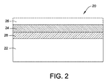
前記誘電体層と界面接触している単結晶半導体デバイス層と、をさらに備え、
前記多層構造のウエハバウは、前記半導体デバイス層のおもて面、および/または、前記単結晶半導体支持基板の裏面の少なくとも3点で測定して、約80マイクロメートルより小さい。

本発明をさらに説明するために、以下の非制限的な実施例を挙げる。
一例では、チョクラルスキー法により成長したインゴットから切り出したシリコンウエハを、SC1溶液を用いて洗浄する。洗浄は、シリコンウエハのおもて面で厚みが0.8nm以上2.0nm以下のシリコン酸化物層が得られるように実施する。次に、化学気相成長チャンバ内にウエハをロードする。850℃以上1000℃以下の温度までウエハを加熱する。設定温度に達した時点で、5秒以上60秒以下(好ましくは、10秒以上40秒以下)の時間、同じ温度でウエハをベーキングする。CVDチャンバ内の周囲雰囲気は、H2、または、H2とエッチングガス(例えば、HClまたはCl2)との組み合わせのいずれかである。還元雰囲気(選択的にエッチングガスを含む)をチャンバに導入し、ウエハの表面の汚染物質を取り除く。ベーキングが完了すると、ウエハに対して、還元雰囲気のベーキングと同じ温度で、多結晶シリコンの化学気相成長法を実施する。多結晶シリコンの化学気相成長用のシリコン前駆体の例は、トリクロロシラン、ジクロロシラン、シランおよびこれらの誘導体である。多結晶シリコンの化学気相成長は、大気圧下または減圧下で行う。成長速度は、0.1μm/分以上2μm/分以下である。多結晶層について所望の厚み(0.5マイクロメートル以上3マイクロメートル以下であってよい)を達成した後、アンロードする上で安全な温度(700℃以上900℃以下)までウエハを冷却する。
一例では、チョクラルスキー法により成長したインゴットから切り出したシリコンウエハを、SC1溶液を用いて洗浄する。洗浄は、シリコンウエハのおもて面で厚みが0.8nm以上2.0nm以下のシリコン酸化物層が得られるように実施する。次に、化学気相成長チャンバ内にウエハをロードする。850℃以上1000℃以下の温度までウエハを加熱する。設定温度に達した時点で、5秒以上60秒以下(好ましくは、10秒以上40秒以下)の時間、同じ温度でウエハをベーキングする。CVDチャンバ内の周囲雰囲気は、H2、または、H2とエッチングガス(例えば、HClまたはCl2)との組み合わせのいずれかである。還元雰囲気(選択的にエッチングガスを含む)をチャンバに導入し、ウエハの表面の汚染物質を取り除く。ベーキングが完了すると、ウエハに対して、還元雰囲気のベーキングと同じ温度で、多結晶シリコンの化学気相成長法を実施する。多結晶シリコンの化学気相成長用のシリコン前駆体の例は、トリクロロシラン、ジクロロシラン、シランおよびこれらの誘導体である。多結晶シリコンの化学気相成長は、大気圧下または減圧下で行う。成長速度は、0.1μm/分以上2μm/分以下である。多結晶シリコンを所望の厚みまで堆積させた後、堆積温度よりも高い温度までウエハ温度を上昇させ、アニールにより残留膜応力を除く。有効に膜応力を解放するための温度は、1000℃またはそれ以上(例えば、1050℃または1100℃)である。アニールの均熱時間(soak time)は、10秒またはそれ以上である。アニールが完了すると、アンロードを行う上で安全な温度までウエハを冷却する。ここで、図5を参照する。図5は、多結晶シリコンの堆積とアニールの条件に対するウエハのワープの依存性を示すグラフである。多結晶シリコン膜における残留膜応力は、ウエハバウとウエハワープの仕様(典型的には、200mmウエハと300mmウエハの両方で、60μm未満である)に適合するように酸化物のベーキング、成長温度、成長速度および堆積後アニールの条件を調節することにより、0から100MPaの範囲で制御できる。所定の膜応力について、ウエハバウとウエハワープは膜厚に比例して増加する。それゆえ、開示している多結晶シリコンの処理により、厚みが最大数十マイクロメートルの多結晶シリコン膜を成長させることができる。多結晶層について所望の厚み(0.5マイクロメートル以上3マイクロメートル以下であってよい)を達成した後、アニールを行い、アンロードする上で安全な温度(700℃以上900℃以下)までウエハを冷却する。
一例では、チョクラルスキー法により成長したインゴットから切り出したシリコンウエハを、SC1溶液を用いて洗浄する。洗浄は、シリコンウエハのおもて面で厚みが0.8nm以上2.0nm以下のシリコン酸化物層が得られるように実施する。次に、化学気相成長チャンバ内にウエハをロードする。850℃以上1000℃以下の温度までウエハを加熱する。設定温度に達した時点で、5秒以上60秒以下(好ましくは、10秒以上40秒以下)の時間、同じ温度でウエハをベーキングする。CVDチャンバ内の周囲雰囲気は、H2、または、H2とエッチングガス(例えば、HClまたはCl2)との組み合わせのいずれかである。還元雰囲気(選択的にエッチングガスを含む)をチャンバに導入し、ウエハの表面の汚染物質を取り除く。ベーキングが完了すると、ウエハに対して、還元雰囲気のベーキングと同じ温度で、多結晶シリコンシードの化学気相成長法を実施する。シード層の厚みは、10nm以上200nmである。シード層を所望の厚みまで堆積させた後、温度を上昇させ、アニールにより残留膜応力を取り除く。シード層の厚みは、多結晶シリコンの核の大きさにより設定する。応力を効果的に解放するために、シード層は、50nmより小さいボイドを残しつつ、基板表面をカバーする必要がある。これにより、多結晶シリコンシード層と酸化物との界面へのH2のアクセスが可能となる。H2は界面酸化物を減らし、多結晶シリコンシード層の粒界にある原子が基板へ拡散するのを促進し、これにより膜応力を解放する。シード層が、H2の界面酸化物へのアクセスを完全に妨げるのに十分な厚みを有している場合、後段のアニールプロセスでは膜応力を有効に解放できない。一方、シード層が連続的でなく、隣接する2つの核の間の開口部が50nmよりも大きい場合、シードアニールプロセス中に酸化物層が除去された後に大きい核が形成される。大きい核は成長して、多結晶シリコン堆積の最後には大きい粒(すなわち、直径が1μmより大きい)となり、トラップ効率が低下する。実施例2と比較して、この実施例3では、膜応力を設計するための追加のインサイチュ制御機構が得られる。有効に膜応力を解放するための温度は、1000℃またはそれ以上(例えば、1050℃または1100℃)である。アニールの均熱時間は、10秒またはそれ以上(例えば30秒)である。次に、温度を低下させ、850℃以上1000℃以下とする。低下したこの温度で、多結晶シリコン層の残りを堆積させる。所望の厚みを有する多結晶シリコンを堆積させた後、アンロードを行う上で安全な温度までウエハを冷却する。多結晶層について所望の厚み(0.5マイクロメートル以上3マイクロメートル以下であってよい)を達成した後、アンロードする上で安全な温度(700℃以上900℃以下)までウエハを冷却する。
Claims (60)
- 多層構造を準備する方法であって、
前記方法は、
単結晶半導体支持基板のおもて面に界面接触する半導体酸化物層を形成するステップを含み、
前記単結晶半導体支持基板は、互いに略平行な表面である2つの主面を有し、該2つの主面のうち一方は前記単結晶半導体支持基板のおもて面であり、他方は前記単結晶半導体支持基板の裏面であり、前記単結晶半導体支持基板は、さらに、前記単結晶半導体支持基板のおもて面と裏面とを接続する周縁部と、前記単結晶半導体支持基板のおもて面と裏面との間に位置する中央平面と、前記単結晶半導体支持基板のおもて面と裏面との間に位置するバルク領域とを有し、前記単結晶半導体支持基板の最小バルク領域抵抗率は、500ohm−cm以上であり、
前記方法は、
前記半導体酸化物層がおもて面に界面接触している前記単結晶半導体支持基板を、水素、塩化水素、塩素およびこれらの任意の組み合わせから成る群から選択されるガスを含む周囲雰囲気内でアニールするステップであって、前記半導体酸化物層を含む前記単結晶半導体支持基板のアニールは、大きさが約5ナノメートル以上約1000ナノメートル以下の穴を含む凹凸のある半導体酸化物層を形成するステップと、
前記単結晶半導体支持基板のおもて面に界面接触している凹凸のある半導体酸化物層の上に、多結晶シリコン層を化学気相成長法により堆積させるステップと、
単結晶半導体ドナー基板のおもて面の上に位置する誘電体層を、前記単結晶半導体支持基板の多結晶シリコン層に接合させ、これにより接合構造を形成するステップとを含み、
前記単結晶半導体ドナー基板は、互いに略平行な表面である2つの主面を有し、該2つの主面のうち一方は前記単結晶半導体ドナー基板のおもて面であり、他方は前記単結晶半導体ドナー基板の裏面であり、前記単結晶半導体ドナー基板は、さらに、前記単結晶半導体ドナー基板のおもて面と裏面とを接続する周縁部と、前記単結晶半導体ドナー基板のおもて面と裏面との間に位置する中央平面とを有する、
方法。 - 前記単結晶半導体支持基板は、シリコンを含み、
前記半導体酸化物層は、二酸化ケイ素を含む、
請求項1に記載の方法。 - 前記単結晶半導体支持基板は、チョクラルスキー法またはフロートゾーン法により成長した単結晶シリコンインゴットから切り出されたシリコンウエハを含み、
前記半導体酸化物は、二酸化ケイ素を含む、
請求項1に記載の方法。 - 前記半導体酸化物層は、前記単結晶半導体支持基板のおもて面の上に堆積させ、
前記半導体酸化物層は、空気、オゾン、および、酸化剤を含む水性組成物から成る群から選択される酸化性媒質に前記単結晶半導体支持基板を曝露することにより形成する、
請求項1に記載の方法。 - 前記半導体酸化物層の厚みは、約0.1ナノメートル以上約25ナノメートル以下である、
請求項4に記載の方法。 - 前記半導体酸化物層の厚みは、約0.5ナノメートル以上約5ナノメートル以下である、
請求項4に記載の方法。 - 前記単結晶半導体支持基板のバルク抵抗率は、約500Ohm−cm以上約100000Ohm−cm以下であり、または、約1000Ohm−cm以上約100000Ohm−cm以下である、
請求項1に記載の方法。 - 前記単結晶半導体支持基板のバルク抵抗率は、約1000Ohm−cm以上約10000Ohm−cm以下、または、約2000Ohm−cm以上約10000Ohm−cm以下である、
請求項1に記載の方法。 - 前記単結晶半導体支持基板のバルク抵抗率は、約3000Ohm−cm以上約10000Ohm−cm以下、または、約3000Ohm−cm以上約5000Ohm−cm以下である、
請求項1に記載の方法。 - 前記単結晶半導体支持基板のおもて面には、前記半導体酸化物層が設けられ、
前記半導体酸化物層は、水素、塩化水素、塩素およびこれらの任意の組み合わせから成る群から選択されるガスを含む周囲雰囲気において、約850℃より高い温度でアニールする、
請求項1に記載の方法。 - 前記単結晶半導体支持基板のおもて面には、前記半導体酸化物層が設けられ、
前記半導体酸化物層は、水素、塩化水素、塩素およびこれらの任意の組み合わせから成る群から選択されるガスを含む周囲雰囲気において、約850℃以上約1000℃以下の温度でアニールする、
請求項1に記載の方法。 - 前記多結晶シリコン層は、シラン、トリクロロシラン、ジクロロシランおよびこれらの任意の組み合わせから成る群から選択されるシリコン前駆体を含む成長周囲雰囲気から、約0.1マイクロメートル/分以上の成長速度で堆積させる、
請求項1に記載の方法。 - 前記多結晶シリコン層は、シラン、トリクロロシラン、ジクロロシランおよびこれらの任意の組み合わせから成る群から選択されるシリコン前駆体を含む成長周囲雰囲気から、約0.1マイクロメートル/分以上約2マイクロメートル/分以下の成長速度で堆積させる、
請求項1に記載の方法。 - 化学気相成長法による前記多結晶シリコン層の堆積は、多結晶シリコンシード層を堆積させた後に中断し、
前記多結晶シリコンシード層は、約1000℃より高い温度でアニールする、
請求項1に記載の方法。 - 前記多結晶シリコンシード層の厚みは、3マイクロメートルより小さい、
請求項14に記載の方法。 - 化学気相成長法による前記多結晶シリコン層の堆積は、前記単結晶半導体支持基板を約850℃以上約1000℃以下まで冷却した後に再開する、
請求項14に記載の方法。 - 化学気相成長法による前記多結晶シリコン層の堆積は、多結晶シリコンシード層を堆積させた後に中断し、
前記多結晶シリコンシード層は、約1000℃以上約1100℃以下の温度でアニールする、
請求項1に記載の方法。 - 前記多結晶シリコンシード層の厚みは、3マイクロメートルより小さい、
請求項17に記載の方法。 - 化学気相成長法による前記多結晶シリコン層の堆積は、前記単結晶半導体支持基板を約850℃以上約1000℃以下まで冷却した後に再開する、
請求項17に記載の方法。 - 前記多結晶シリコン層の厚みは、約0.1マイクロメートル以上約50マイクロメートル以下である、
請求項1に記載の方法。 - 前記多結晶シリコン層の厚みは、約0.1マイクロメートル以上約20マイクロメートル以下である、
請求項1に記載の方法。 - 前記多結晶シリコン層の厚みは、約0.1マイクロメートル以上約10マイクロメートル以下である、
請求項1に記載の方法。 - 前記多結晶シリコン層の厚みは、約0.5マイクロメートル以上約5マイクロメートル以下である、
請求項1に記載の方法。 - 前記多結晶シリコン層は、約850℃より高い温度で堆積させる、
請求項1に記載の方法。 - 前記多結晶シリコン層は、約850℃以上約1000℃以下で堆積させる、
請求項1に記載の方法。 - 前記堆積した多結晶シリコン層を約1000℃より高い温度でアニールするステップをさらに含む、
請求項1に記載の方法。 - 前記堆積した多結晶シリコン層を約1000℃以上約1100℃以下の温度でアニールするステップをさらに含む、
請求項1に記載の方法。 - 前記堆積した多結晶シリコン層を、RMS2x2 um2で測定した表面粗さが約5オングストロームより小さくなるまで研磨するステップをさらに含む、
請求項1に記載の方法。 - 前記単結晶半導体ドナー基板のおもて面の上に位置する誘電体層に接合させる前に、前記多結晶シリコン層を酸化させるステップをさらに含む、
請求項1に記載の方法。 - 前記半導体ドナー基板の誘電体層と、前記単結晶半導体支持基板のおもて面に界面接触する凹凸のある半導体酸化物層の上の前記多結晶シリコン層との接合を強化するのに十分な温度と時間、前記接合構造を加熱するステップをさらに含む、
請求項1に記載の方法。 - 前記単結晶半導体ドナー基板は、イオン注入されたダメージ層を含む、
請求項1に記載の方法。 - 前記単結晶半導体ドナー基板のイオン注入ダメージ層の位置で、前記接合構造を機械的に割断し、前記単結晶半導体支持基板、前記凹凸のある半導体酸化物層、前記多結晶シリコン層、前記多結晶シリコン層に接触している前記誘電体層、および前記誘電体層に接触している単結晶半導体デバイス層を含む割断構造を準備するステップをさらに含む、
請求項31に記載の方法。 - 前記単結晶半導体デバイス層と前記単結晶半導体支持基板との接合を強化するのに十分な温度と時間、前記割断構造を加熱するステップをさらに含む、
請求項32に記載の方法。 - 多層構造を準備する方法であって、
前記方法は、
単結晶半導体支持基板のおもて面に界面接触する半導体酸化物層を形成するステップを含み、
前記単結晶半導体支持基板は、互いに略平行な表面である2つの主面を有し、該2つの主面のうち一方は前記単結晶半導体支持基板のおもて面であり、他方は前記単結晶半導体支持基板の裏面であり、前記単結晶半導体支持基板は、さらに、前記単結晶半導体支持基板のおもて面と裏面とを接続する周縁部と、前記単結晶半導体支持基板のおもて面と裏面との間に位置する中央平面と、前記単結晶半導体支持基板のおもて面と裏面との間に位置するバルク領域とを有し、前記単結晶半導体支持基板の最小バルク領域抵抗率は、500ohm−cm以上であり、
前記方法は、
前記半導体酸化物層がおもて面に界面接触している前記単結晶半導体支持基板を、水素、塩化水素、塩素およびこれらの任意の組み合わせから成る群から選択されるガスを含む周囲雰囲気内でアニールするステップであって、前記半導体酸化物層を含む前記単結晶半導体支持基板のアニールは、大きさが約5ナノメートル以上約1000ナノメートル以下の穴を含む凹凸のある半導体酸化物層を形成するステップと、
前記凹凸のある半導体酸化物層がおもて面に界面接触している前記単結晶半導体支持基板を、シリコン前駆体を含む約850℃以上の周囲雰囲気に曝露し、前記凹凸のある半導体酸化物層の上に多結晶シリコン層を堆積させるステップと、
単結晶半導体ドナー基板のおもて面の上に位置する誘電体層を、前記単結晶半導体支持基板の多結晶シリコン層に接合させ、これにより接合構造を形成するステップとを含み、
前記単結晶半導体ドナー基板は、互いに略平行な表面である2つの主面を有し、該2つの主面のうち一方は前記単結晶半導体ドナー基板のおもて面であり、他方は前記単結晶半導体ドナー基板の裏面であり、前記単結晶半導体ドナー基板は、さらに、前記単結晶半導体ドナー基板のおもて面と裏面とを接続する周縁部と、前記単結晶半導体ドナー基板のおもて面と裏面との間に位置する中央平面とを有する、
方法。 - 前記単結晶半導体支持基板は、シリコンを含み、
前記半導体酸化物層は、二酸化ケイ素を含む、
請求項34に記載の方法。 - 前記単結晶半導体支持基板は、チョクラルスキー法またはフロートゾーン法により成長した単結晶シリコンインゴットから切り出されたシリコンウエハを含み、
前記半導体酸化物は、二酸化ケイ素を含む、
請求項34に記載の方法。 - 前記半導体酸化物層は、前記単結晶半導体支持基板のおもて面の上に堆積させ、
前記半導体酸化物層は、空気、オゾン、および、酸化剤を含む水性組成物から成る群から選択される酸化性媒質に前記単結晶半導体支持基板を曝露することにより形成する、
請求項34に記載の方法。 - 前記半導体酸化物層の厚みは、約0.1ナノメートル以上約25ナノメートル以下である、
請求項34に記載の方法。 - 前記半導体酸化物層の厚みは、約0.5ナノメートル以上約5ナノメートル以下である、
請求項34に記載の方法。 - 前記単結晶半導体支持基板のバルク抵抗率は、約500Ohm−cm以上約100000Ohm−cm以下であり、または、約1000Ohm−cm以上約100000Ohm−cm以下である、
請求項34に記載の方法。 - 前記単結晶半導体支持基板のバルク抵抗率は、約1000Ohm−cm以上約10000Ohm−cm以下、または、約2000Ohm−cm以上約10000Ohm−cm以下である、
請求項34に記載の方法。 - 前記単結晶半導体支持基板のバルク抵抗率は、約3000Ohm−cm以上約10000Ohm−cm以下、または、約3000Ohm−cm以上約5000Ohm−cm以下である、
請求項34に記載の方法。 - 前記単結晶半導体支持基板のおもて面には、前記半導体酸化物層が設けられ、
前記半導体酸化物層は、水素、塩化水素、塩素およびこれらの任意の組み合わせから成る群から選択されるガスを含む周囲雰囲気において、約850℃より高い温度でアニールする、
請求項34に記載の方法。 - 前記単結晶半導体支持基板のおもて面には、前記半導体酸化物層が設けられ、
前記半導体酸化物層は、水素、塩化水素、塩素およびこれらの任意の組み合わせから成る群から選択されるガスを含む周囲雰囲気において、約850℃以上約1000℃以下の温度でアニールする、
請求項34に記載の方法。 - 前記シリコン前駆体は、シラン、トリクロロシラン、ジクロロシランおよびこれらの任意の組み合わせから成る群から選択され、
前記多結晶シリコン層は、約0.1マイクロメートル/分以上の成長速度で堆積させる、
請求項34に記載の方法。 - 前記シリコン前駆体は、シラン、トリクロロシラン、ジクロロシランおよびこれらの任意の組み合わせから成る群から選択され、
前記多結晶シリコン層は、約0.1マイクロメートル/分以上約2マイクロメートル/分以下の成長速度で堆積させる、
請求項34に記載の方法。 - 前記多結晶シリコン層の堆積は、多結晶シリコンシード層を約3マイクロメートル堆積させた後に中断し、
前記多結晶シリコンシード層は、約1000℃より高い温度でアニールする、
請求項34に記載の方法。 - 前記多結晶シリコン層の厚みは、約0.1マイクロメートル以上約50マイクロメートル以下である、
請求項34に記載の方法。 - 前記多結晶シリコン層の厚みは、約0.1マイクロメートル以上約20マイクロメートル以下である、
請求項34に記載の方法。 - 前記多結晶シリコン層の厚みは、約0.1マイクロメートル以上約10マイクロメートル以下である、
請求項34に記載の方法。 - 前記多結晶シリコン層の厚みは、約0.5マイクロメートル以上約5マイクロメートル以下である、
請求項34に記載の方法。 - 前記多結晶シリコン層は、約850℃以上約1000℃以下で堆積させる、
請求項34に記載の方法。 - 前記堆積した多結晶シリコン層を約1000℃より高い温度でアニールするステップをさらに含む、
請求項34に記載の方法。 - 前記堆積した多結晶シリコン層を約1000℃以上約1100℃以下の温度でアニールするステップをさらに含む、
請求項34に記載の方法。 - 前記堆積した多結晶シリコン層を、RMS2x2 um2で測定した表面粗さが約5オングストロームより小さくなるまで研磨するステップをさらに含む、
請求項34に記載の方法。 - 前記単結晶半導体ドナー基板のおもて面の上に設けられた誘電体層に接合させる前に、前記多結晶シリコン層を酸化させるステップをさらに含む、
請求項34に記載の方法。 - 前記半導体ドナー基板の誘電体層と、前記単結晶半導体支持基板のおもて面に界面接触する凹凸のある半導体酸化物層の上の前記多結晶シリコン層との接合を強化するのに十分な温度と時間、前記接合構造を加熱するステップをさらに含む、
請求項34に記載の方法。 - 前記単結晶半導体ドナー基板は、イオン注入されたダメージ層を含む、
請求項34に記載の方法。 - 前記単結晶半導体ドナー基板のイオン注入ダメージ層の位置で、前記接合構造を機械的に割断し、前記単結晶半導体支持基板、前記凹凸のある半導体酸化物層、前記多結晶シリコン層、前記多結晶シリコン層に接触している前記誘電体層、および前記誘電体層に接触している単結晶半導体デバイス層を含む割断構造を準備するステップをさらに含む、
請求項58に記載の方法。 - 前記単結晶半導体デバイス層と前記多結晶シリコン層との接合を強化するのに十分な温度と時間、前記割断構造を加熱するステップをさらに含む、
請求項59に記載の方法。
Applications Claiming Priority (3)
| Application Number | Priority Date | Filing Date | Title |
|---|---|---|---|
| US201562127418P | 2015-03-03 | 2015-03-03 | |
| US62/127,418 | 2015-03-03 | ||
| PCT/US2016/019464 WO2016140850A1 (en) | 2015-03-03 | 2016-02-25 | Method of depositing charge trapping polycrystalline silicon films on silicon substrates with controllable film stress |
Related Child Applications (1)
| Application Number | Title | Priority Date | Filing Date |
|---|---|---|---|
| JP2019078624A Division JP6796162B2 (ja) | 2015-03-03 | 2019-04-17 | 膜応力を制御可能なシリコン基板の上に電荷トラップ用多結晶シリコン膜を成長させる方法 |
Publications (3)
| Publication Number | Publication Date |
|---|---|
| JP2018507562A JP2018507562A (ja) | 2018-03-15 |
| JP2018507562A5 JP2018507562A5 (ja) | 2019-04-11 |
| JP6517360B2 true JP6517360B2 (ja) | 2019-05-22 |
Family
ID=55755658
Family Applications (2)
| Application Number | Title | Priority Date | Filing Date |
|---|---|---|---|
| JP2017546134A Active JP6517360B2 (ja) | 2015-03-03 | 2016-02-25 | 膜応力を制御可能なシリコン基板の上に電荷トラップ用多結晶シリコン膜を成長させる方法 |
| JP2019078624A Active JP6796162B2 (ja) | 2015-03-03 | 2019-04-17 | 膜応力を制御可能なシリコン基板の上に電荷トラップ用多結晶シリコン膜を成長させる方法 |
Family Applications After (1)
| Application Number | Title | Priority Date | Filing Date |
|---|---|---|---|
| JP2019078624A Active JP6796162B2 (ja) | 2015-03-03 | 2019-04-17 | 膜応力を制御可能なシリコン基板の上に電荷トラップ用多結晶シリコン膜を成長させる方法 |
Country Status (6)
| Country | Link |
|---|---|
| US (3) | US10283402B2 (ja) |
| EP (3) | EP3266038B1 (ja) |
| JP (2) | JP6517360B2 (ja) |
| CN (1) | CN107533953B (ja) |
| TW (1) | TWI711067B (ja) |
| WO (1) | WO2016140850A1 (ja) |
Cited By (1)
| Publication number | Priority date | Publication date | Assignee | Title |
|---|---|---|---|---|
| TWI828929B (zh) * | 2019-07-15 | 2024-01-11 | 法商索泰克公司 | 用於基材之親水性接合的方法 |
Families Citing this family (27)
| Publication number | Priority date | Publication date | Assignee | Title |
|---|---|---|---|---|
| CN107533953B (zh) * | 2015-03-03 | 2021-05-11 | 环球晶圆股份有限公司 | 具有可控膜应力的在硅衬底上沉积电荷捕获多晶硅膜的方法 |
| JP6592534B2 (ja) * | 2015-06-01 | 2019-10-16 | サンエディソン・セミコンダクター・リミテッドSunEdison Semiconductor Limited | 多層構造体及びその製造方法 |
| FR3037443B1 (fr) * | 2015-06-12 | 2018-07-13 | Soitec | Heterostructure et methode de fabrication |
| JP6447439B2 (ja) * | 2015-09-28 | 2019-01-09 | 信越半導体株式会社 | 貼り合わせsoiウェーハの製造方法 |
| WO2017142849A1 (en) * | 2016-02-19 | 2017-08-24 | Sunedison Semiconductor Limited | Semiconductor on insulator structure comprising a buried high resistivity layer |
| US20180019169A1 (en) * | 2016-07-12 | 2018-01-18 | QMAT, Inc. | Backing substrate stabilizing donor substrate for implant or reclamation |
| SG10201913059PA (en) * | 2016-12-05 | 2020-02-27 | Globalwafers Co Ltd | High resistivity silicon-on-insulator structure and method of manufacture thereof |
| FR3062238A1 (fr) * | 2017-01-26 | 2018-07-27 | Soitec | Support pour une structure semi-conductrice |
| US10468486B2 (en) | 2017-10-30 | 2019-11-05 | Taiwan Semiconductor Manufacturing Company Ltd. | SOI substrate, semiconductor device and method for manufacturing the same |
| KR102562239B1 (ko) * | 2018-04-27 | 2023-07-31 | 글로벌웨이퍼스 씨오., 엘티디. | 반도체 도너 기판으로부터의 층 전이를 용이하게 하는 광 지원형 소판 형성 |
| CN112262467A (zh) * | 2018-06-08 | 2021-01-22 | 环球晶圆股份有限公司 | 将硅薄层移转的方法 |
| JP6827442B2 (ja) * | 2018-06-14 | 2021-02-10 | 信越半導体株式会社 | 貼り合わせsoiウェーハの製造方法及び貼り合わせsoiウェーハ |
| JP7230297B2 (ja) * | 2018-07-05 | 2023-03-01 | ソイテック | 集積された高周波デバイスのための基板及びそれを製造するための方法 |
| US10943813B2 (en) * | 2018-07-13 | 2021-03-09 | Globalwafers Co., Ltd. | Radio frequency silicon on insulator wafer platform with superior performance, stability, and manufacturability |
| CN110875171A (zh) * | 2018-08-31 | 2020-03-10 | 北京北方华创微电子装备有限公司 | 多晶硅功能层的制备方法 |
| KR102357328B1 (ko) * | 2018-12-20 | 2022-02-08 | 어플라이드 머티어리얼스, 인코포레이티드 | 도핑된 ⅳ족 재료들을 성장시키는 방법 |
| FR3098642B1 (fr) * | 2019-07-12 | 2021-06-11 | Soitec Silicon On Insulator | procédé de fabrication d'une structure comprenant une couche mince reportée sur un support muni d’une couche de piégeage de charges |
| CN110400743A (zh) * | 2019-08-15 | 2019-11-01 | 上海新傲科技股份有限公司 | 多晶硅薄膜半导体衬底的制备方法 |
| CN113711335A (zh) * | 2019-11-14 | 2021-11-26 | 华为数字能源技术有限公司 | 半导体衬底及其制造方法、半导体器件 |
| EP3840033A1 (fr) * | 2019-12-17 | 2021-06-23 | Commissariat à l'énergie atomique et aux énergies alternatives | Procédé de fabrication d'un substrat rf-soi à couche de piégeage issue d'une transformation cristalline d'une couche enterrée |
| JP7192757B2 (ja) * | 2019-12-19 | 2022-12-20 | 株式会社Sumco | エピタキシャルシリコンウェーハ及びその製造方法並びにx線検出センサ |
| JP7380179B2 (ja) * | 2019-12-19 | 2023-11-15 | 株式会社Sumco | 多層soiウェーハ及びその製造方法並びにx線検出センサ |
| JP2021190660A (ja) * | 2020-06-04 | 2021-12-13 | 株式会社Sumco | 貼り合わせウェーハ用の支持基板 |
| US20220115226A1 (en) * | 2020-10-08 | 2022-04-14 | Okmetic Oy | Manufacture method of a high-resistivity silicon handle wafer for a hybrid substrate structure |
| FR3117668B1 (fr) * | 2020-12-16 | 2022-12-23 | Commissariat Energie Atomique | Structure amelioree de substrat rf et procede de realisation |
| TWI792295B (zh) * | 2021-05-04 | 2023-02-11 | 合晶科技股份有限公司 | 半導體基板及其製造方法 |
| EP4287239A1 (en) * | 2022-06-02 | 2023-12-06 | Imec VZW | A low loss semiconductor substrate |
Family Cites Families (89)
| Publication number | Priority date | Publication date | Assignee | Title |
|---|---|---|---|---|
| US4501060A (en) | 1983-01-24 | 1985-02-26 | At&T Bell Laboratories | Dielectrically isolated semiconductor devices |
| FR2580673B1 (fr) * | 1985-04-19 | 1987-09-25 | Haond Michel | Procede de fabrication sur un support isolant d'un film de silicium monocristallin oriente et a defauts localises |
| JPS6265317A (ja) * | 1985-09-17 | 1987-03-24 | Mitsubishi Electric Corp | 半導体単結晶膜形成のためのウエハ構造 |
| US4755865A (en) | 1986-01-21 | 1988-07-05 | Motorola Inc. | Means for stabilizing polycrystalline semiconductor layers |
| US4760036A (en) * | 1987-06-15 | 1988-07-26 | Delco Electronics Corporation | Process for growing silicon-on-insulator wafers using lateral epitaxial growth with seed window oxidation |
| JPH0648686B2 (ja) * | 1988-03-30 | 1994-06-22 | 新日本製鐵株式会社 | ゲッタリング能力の優れたシリコンウェーハおよびその製造方法 |
| US5189508A (en) * | 1988-03-30 | 1993-02-23 | Nippon Steel Corporation | Silicon wafer excelling in gettering ability and method for production thereof |
| JPH06105691B2 (ja) | 1988-09-29 | 1994-12-21 | 株式会社富士電機総合研究所 | 炭素添加非晶質シリコン薄膜の製造方法 |
| JP2617798B2 (ja) | 1989-09-22 | 1997-06-04 | 三菱電機株式会社 | 積層型半導体装置およびその製造方法 |
| US6043138A (en) | 1996-09-16 | 2000-03-28 | Advanced Micro Devices, Inc. | Multi-step polysilicon deposition process for boron penetration inhibition |
| US5783469A (en) | 1996-12-10 | 1998-07-21 | Advanced Micro Devices, Inc. | Method for making nitrogenated gate structure for improved transistor performance |
| JP3171322B2 (ja) * | 1997-03-11 | 2001-05-28 | 日本電気株式会社 | Soi基板およびその製造方法 |
| US6068928A (en) | 1998-02-25 | 2000-05-30 | Siemens Aktiengesellschaft | Method for producing a polycrystalline silicon structure and polycrystalline silicon layer to be produced by the method |
| US6479166B1 (en) * | 1998-10-06 | 2002-11-12 | Case Western Reserve University | Large area polysilicon films with predetermined stress characteristics and method for producing same |
| US6268068B1 (en) | 1998-10-06 | 2001-07-31 | Case Western Reserve University | Low stress polysilicon film and method for producing same |
| JP4313874B2 (ja) | 1999-02-02 | 2009-08-12 | キヤノン株式会社 | 基板の製造方法 |
| US6204205B1 (en) * | 1999-07-06 | 2001-03-20 | Taiwan Semiconductor Manufacturing Company | Using H2anneal to improve the electrical characteristics of gate oxide |
| US20020090758A1 (en) | 2000-09-19 | 2002-07-11 | Silicon Genesis Corporation | Method and resulting device for manufacturing for double gated transistors |
| US20050026432A1 (en) | 2001-04-17 | 2005-02-03 | Atwater Harry A. | Wafer bonded epitaxial templates for silicon heterostructures |
| US6562127B1 (en) | 2002-01-16 | 2003-05-13 | The United States Of America As Represented By The Secretary Of The Navy | Method of making mosaic array of thin semiconductor material of large substrates |
| US6995430B2 (en) | 2002-06-07 | 2006-02-07 | Amberwave Systems Corporation | Strained-semiconductor-on-insulator device structures |
| US7074623B2 (en) | 2002-06-07 | 2006-07-11 | Amberwave Systems Corporation | Methods of forming strained-semiconductor-on-insulator finFET device structures |
| US6743662B2 (en) | 2002-07-01 | 2004-06-01 | Honeywell International, Inc. | Silicon-on-insulator wafer for RF integrated circuit |
| US7057234B2 (en) | 2002-12-06 | 2006-06-06 | Cornell Research Foundation, Inc. | Scalable nano-transistor and memory using back-side trapping |
| WO2004061944A1 (en) | 2003-01-07 | 2004-07-22 | S.O.I.Tec Silicon On Insulator Technologies | Recycling of a wafer comprising a multi-layer structure after taking-off a thin layer |
| US7005160B2 (en) * | 2003-04-24 | 2006-02-28 | Asm America, Inc. | Methods for depositing polycrystalline films with engineered grain structures |
| CN1856873A (zh) | 2003-09-26 | 2006-11-01 | 卢万天主教大学 | 制造具有降低的欧姆损耗的多层半导体结构的方法 |
| FR2860341B1 (fr) * | 2003-09-26 | 2005-12-30 | Soitec Silicon On Insulator | Procede de fabrication de structure multicouche a pertes diminuees |
| US6992025B2 (en) | 2004-01-12 | 2006-01-31 | Sharp Laboratories Of America, Inc. | Strained silicon on insulator from film transfer and relaxation by hydrogen implantation |
| US7279400B2 (en) | 2004-08-05 | 2007-10-09 | Sharp Laboratories Of America, Inc. | Method of fabricating single-layer and multi-layer single crystalline silicon and silicon devices on plastic using sacrificial glass |
| US7312487B2 (en) | 2004-08-16 | 2007-12-25 | International Business Machines Corporation | Three dimensional integrated circuit |
| DE102004041378B4 (de) * | 2004-08-26 | 2010-07-08 | Siltronic Ag | Halbleiterscheibe mit Schichtstruktur mit geringem Warp und Bow sowie Verfahren zu ihrer Herstellung |
| US7476594B2 (en) | 2005-03-30 | 2009-01-13 | Cree, Inc. | Methods of fabricating silicon nitride regions in silicon carbide and resulting structures |
| FR2890489B1 (fr) | 2005-09-08 | 2008-03-07 | Soitec Silicon On Insulator | Procede de fabrication d'une heterostructure de type semi-conducteur sur isolant |
| FR2897982B1 (fr) | 2006-02-27 | 2008-07-11 | Tracit Technologies Sa | Procede de fabrication des structures de type partiellement soi, comportant des zones reliant une couche superficielle et un substrat |
| US7964514B2 (en) * | 2006-03-02 | 2011-06-21 | Applied Materials, Inc. | Multiple nitrogen plasma treatments for thin SiON dielectrics |
| FR2902233B1 (fr) | 2006-06-09 | 2008-10-17 | Soitec Silicon On Insulator | Procede de limitation de diffusion en mode lacunaire dans une heterostructure |
| FR2911430B1 (fr) | 2007-01-15 | 2009-04-17 | Soitec Silicon On Insulator | "procede de fabrication d'un substrat hybride" |
| WO2008149699A1 (en) | 2007-06-01 | 2008-12-11 | Semiconductor Energy Laboratory Co., Ltd. | Manufacturing method of semiconductor substrate and semiconductor device |
| JP4445524B2 (ja) | 2007-06-26 | 2010-04-07 | 株式会社東芝 | 半導体記憶装置の製造方法 |
| JP2009016692A (ja) | 2007-07-06 | 2009-01-22 | Toshiba Corp | 半導体記憶装置の製造方法と半導体記憶装置 |
| US20090278233A1 (en) | 2007-07-26 | 2009-11-12 | Pinnington Thomas Henry | Bonded intermediate substrate and method of making same |
| US7915716B2 (en) | 2007-09-27 | 2011-03-29 | Stats Chippac Ltd. | Integrated circuit package system with leadframe array |
| US7879699B2 (en) | 2007-09-28 | 2011-02-01 | Infineon Technologies Ag | Wafer and a method for manufacturing a wafer |
| US8128749B2 (en) | 2007-10-04 | 2012-03-06 | International Business Machines Corporation | Fabrication of SOI with gettering layer |
| US7868419B1 (en) | 2007-10-18 | 2011-01-11 | Rf Micro Devices, Inc. | Linearity improvements of semiconductor substrate based radio frequency devices |
| JP2009135453A (ja) | 2007-10-30 | 2009-06-18 | Semiconductor Energy Lab Co Ltd | 半導体装置の作製方法、半導体装置及び電子機器 |
| US7883990B2 (en) * | 2007-10-31 | 2011-02-08 | International Business Machines Corporation | High resistivity SOI base wafer using thermally annealed substrate |
| US20090236689A1 (en) | 2008-03-24 | 2009-09-24 | Freescale Semiconductor, Inc. | Integrated passive device and method with low cost substrate |
| FR2933234B1 (fr) | 2008-06-30 | 2016-09-23 | S O I Tec Silicon On Insulator Tech | Substrat bon marche a structure double et procede de fabrication associe |
| FR2933233B1 (fr) * | 2008-06-30 | 2010-11-26 | Soitec Silicon On Insulator | Substrat de haute resistivite bon marche et procede de fabrication associe |
| US8058137B1 (en) | 2009-04-14 | 2011-11-15 | Monolithic 3D Inc. | Method for fabrication of a semiconductor device and structure |
| JP2010258083A (ja) | 2009-04-22 | 2010-11-11 | Panasonic Corp | Soiウェーハ、その製造方法および半導体装置の製造方法 |
| KR101094554B1 (ko) * | 2009-06-08 | 2011-12-19 | 주식회사 하이닉스반도체 | 불휘발성 메모리 소자의 제조방법 |
| CN105552115B (zh) | 2009-11-02 | 2019-10-29 | 富士电机株式会社 | 半导体器件以及用于制造半导体器件的方法 |
| JP5644096B2 (ja) | 2009-11-30 | 2014-12-24 | ソニー株式会社 | 接合基板の製造方法及び固体撮像装置の製造方法 |
| US8252624B2 (en) | 2010-01-18 | 2012-08-28 | Applied Materials, Inc. | Method of manufacturing thin film solar cells having a high conversion efficiency |
| US9099526B2 (en) | 2010-02-16 | 2015-08-04 | Monolithic 3D Inc. | Integrated circuit device and structure |
| WO2011118643A1 (ja) | 2010-03-26 | 2011-09-29 | テルモ株式会社 | 留置針組立体 |
| US8859393B2 (en) | 2010-06-30 | 2014-10-14 | Sunedison Semiconductor Limited | Methods for in-situ passivation of silicon-on-insulator wafers |
| US8642416B2 (en) | 2010-07-30 | 2014-02-04 | Monolithic 3D Inc. | Method of forming three dimensional integrated circuit devices using layer transfer technique |
| JP5117588B2 (ja) | 2010-09-07 | 2013-01-16 | 株式会社東芝 | 窒化物半導体結晶層の製造方法 |
| JP5627649B2 (ja) | 2010-09-07 | 2014-11-19 | 株式会社東芝 | 窒化物半導体結晶層の製造方法 |
| FR2967812B1 (fr) | 2010-11-19 | 2016-06-10 | S O I Tec Silicon On Insulator Tech | Dispositif electronique pour applications radiofrequence ou de puissance et procede de fabrication d'un tel dispositif |
| US9287353B2 (en) | 2010-11-30 | 2016-03-15 | Kyocera Corporation | Composite substrate and method of manufacturing the same |
| US8536021B2 (en) | 2010-12-24 | 2013-09-17 | Io Semiconductor, Inc. | Trap rich layer formation techniques for semiconductor devices |
| US8481405B2 (en) | 2010-12-24 | 2013-07-09 | Io Semiconductor, Inc. | Trap rich layer with through-silicon-vias in semiconductor devices |
| EP2656388B1 (en) | 2010-12-24 | 2020-04-15 | QUALCOMM Incorporated | Trap rich layer for semiconductor devices |
| US8796116B2 (en) | 2011-01-31 | 2014-08-05 | Sunedison Semiconductor Limited | Methods for reducing the metal content in the device layer of SOI structures and SOI structures produced by such methods |
| KR101870476B1 (ko) | 2011-03-16 | 2018-06-22 | 썬에디슨, 인크. | 핸들 웨이퍼에 고 비저항 영역을 갖는 실리콘-온-인슐레이터 구조체 및 그러한 구조체를 제조하는 방법 |
| FR2973159B1 (fr) * | 2011-03-22 | 2013-04-19 | Soitec Silicon On Insulator | Procede de fabrication d'un substrat de base |
| FR2973158B1 (fr) * | 2011-03-22 | 2014-02-28 | Soitec Silicon On Insulator | Procédé de fabrication d'un substrat de type semi-conducteur sur isolant pour applications radiofréquences |
| FR2980916B1 (fr) | 2011-10-03 | 2014-03-28 | Soitec Silicon On Insulator | Procede de fabrication d'une structure de type silicium sur isolant |
| US9496255B2 (en) | 2011-11-16 | 2016-11-15 | Qualcomm Incorporated | Stacked CMOS chipset having an insulating layer and a secondary layer and method of forming same |
| US8741739B2 (en) | 2012-01-03 | 2014-06-03 | International Business Machines Corporation | High resistivity silicon-on-insulator substrate and method of forming |
| US20130193445A1 (en) | 2012-01-26 | 2013-08-01 | International Business Machines Corporation | Soi structures including a buried boron nitride dielectric |
| US8921209B2 (en) | 2012-09-12 | 2014-12-30 | International Business Machines Corporation | Defect free strained silicon on insulator (SSOI) substrates |
| FR2999801B1 (fr) * | 2012-12-14 | 2014-12-26 | Soitec Silicon On Insulator | Procede de fabrication d'une structure |
| CN103077949B (zh) * | 2013-01-28 | 2016-09-14 | 上海华虹宏力半导体制造有限公司 | 绝缘体上硅射频器件及其制作方法 |
| US9202711B2 (en) | 2013-03-14 | 2015-12-01 | Sunedison Semiconductor Limited (Uen201334164H) | Semiconductor-on-insulator wafer manufacturing method for reducing light point defects and surface roughness |
| US8951896B2 (en) * | 2013-06-28 | 2015-02-10 | International Business Machines Corporation | High linearity SOI wafer for low-distortion circuit applications |
| US9768056B2 (en) | 2013-10-31 | 2017-09-19 | Sunedison Semiconductor Limited (Uen201334164H) | Method of manufacturing high resistivity SOI wafers with charge trapping layers based on terminated Si deposition |
| KR102189611B1 (ko) | 2014-01-23 | 2020-12-14 | 글로벌웨이퍼스 씨오., 엘티디. | 고 비저항 soi 웨이퍼 및 그 제조 방법 |
| WO2015119742A1 (en) | 2014-02-07 | 2015-08-13 | Sunedison Semiconductor Limited | Methods for preparing layered semiconductor structures |
| JP6118757B2 (ja) * | 2014-04-24 | 2017-04-19 | 信越半導体株式会社 | 貼り合わせsoiウェーハの製造方法 |
| JP6179530B2 (ja) * | 2015-01-23 | 2017-08-16 | 信越半導体株式会社 | 貼り合わせsoiウェーハの製造方法 |
| CN107533953B (zh) * | 2015-03-03 | 2021-05-11 | 环球晶圆股份有限公司 | 具有可控膜应力的在硅衬底上沉积电荷捕获多晶硅膜的方法 |
| JP6344271B2 (ja) * | 2015-03-06 | 2018-06-20 | 信越半導体株式会社 | 貼り合わせ半導体ウェーハ及び貼り合わせ半導体ウェーハの製造方法 |
| US9716136B1 (en) * | 2016-03-16 | 2017-07-25 | Globalfoundries Inc. | Embedded polysilicon resistors with crystallization barriers |
-
2016
- 2016-02-25 CN CN201680025562.9A patent/CN107533953B/zh active Active
- 2016-02-25 US US15/554,034 patent/US10283402B2/en active Active
- 2016-02-25 EP EP16716946.5A patent/EP3266038B1/en active Active
- 2016-02-25 EP EP22192385.7A patent/EP4120320A1/en active Pending
- 2016-02-25 EP EP18167041.5A patent/EP3367424B1/en active Active
- 2016-02-25 WO PCT/US2016/019464 patent/WO2016140850A1/en active Application Filing
- 2016-02-25 JP JP2017546134A patent/JP6517360B2/ja active Active
- 2016-03-03 TW TW105106562A patent/TWI711067B/zh active
-
2018
- 2018-11-12 US US16/186,683 patent/US10658227B2/en active Active
-
2019
- 2019-04-17 JP JP2019078624A patent/JP6796162B2/ja active Active
- 2019-12-19 US US16/720,136 patent/US10784146B2/en active Active
Cited By (1)
| Publication number | Priority date | Publication date | Assignee | Title |
|---|---|---|---|---|
| TWI828929B (zh) * | 2019-07-15 | 2024-01-11 | 法商索泰克公司 | 用於基材之親水性接合的方法 |
Also Published As
| Publication number | Publication date |
|---|---|
| EP3266038B1 (en) | 2019-09-25 |
| EP4120320A1 (en) | 2023-01-18 |
| US20180233400A1 (en) | 2018-08-16 |
| CN107533953B (zh) | 2021-05-11 |
| EP3266038A1 (en) | 2018-01-10 |
| US10283402B2 (en) | 2019-05-07 |
| US20200126848A1 (en) | 2020-04-23 |
| JP2018507562A (ja) | 2018-03-15 |
| TW201707051A (zh) | 2017-02-16 |
| US20190096745A1 (en) | 2019-03-28 |
| EP3367424A1 (en) | 2018-08-29 |
| WO2016140850A1 (en) | 2016-09-09 |
| EP3367424B1 (en) | 2022-10-19 |
| CN107533953A (zh) | 2018-01-02 |
| US10784146B2 (en) | 2020-09-22 |
| JP6796162B2 (ja) | 2020-12-02 |
| TWI711067B (zh) | 2020-11-21 |
| JP2019153797A (ja) | 2019-09-12 |
| US10658227B2 (en) | 2020-05-19 |
Similar Documents
| Publication | Publication Date | Title |
|---|---|---|
| JP6517360B2 (ja) | 膜応力を制御可能なシリコン基板の上に電荷トラップ用多結晶シリコン膜を成長させる方法 | |
| TWI721223B (zh) | 具有較佳電荷捕獲效率之高電阻率絕緣體上矽基板 | |
| JP6650463B2 (ja) | 電荷トラップ層を備えた高抵抗率の半導体・オン・インシュレーターウェハーの製造方法 | |
| TWI727123B (zh) | 高電阻率絕緣體上矽結構及其製造方法 | |
| JP7206366B2 (ja) | 高抵抗率半導体・オン・インシュレータウエハおよび製造方法 |
Legal Events
| Date | Code | Title | Description |
|---|---|---|---|
| A521 | Request for written amendment filed |
Free format text: JAPANESE INTERMEDIATE CODE: A523 Effective date: 20190225 |
|
| A621 | Written request for application examination |
Free format text: JAPANESE INTERMEDIATE CODE: A621 Effective date: 20190225 |
|
| A871 | Explanation of circumstances concerning accelerated examination |
Free format text: JAPANESE INTERMEDIATE CODE: A871 Effective date: 20190301 |
|
| A975 | Report on accelerated examination |
Free format text: JAPANESE INTERMEDIATE CODE: A971005 Effective date: 20190311 |
|
| TRDD | Decision of grant or rejection written | ||
| A01 | Written decision to grant a patent or to grant a registration (utility model) |
Free format text: JAPANESE INTERMEDIATE CODE: A01 Effective date: 20190319 |
|
| A61 | First payment of annual fees (during grant procedure) |
Free format text: JAPANESE INTERMEDIATE CODE: A61 Effective date: 20190417 |
|
| R150 | Certificate of patent or registration of utility model |
Ref document number: 6517360 Country of ref document: JP Free format text: JAPANESE INTERMEDIATE CODE: R150 |
|
| S111 | Request for change of ownership or part of ownership |
Free format text: JAPANESE INTERMEDIATE CODE: R313113 |
|
| R350 | Written notification of registration of transfer |
Free format text: JAPANESE INTERMEDIATE CODE: R350 |
|
| R250 | Receipt of annual fees |
Free format text: JAPANESE INTERMEDIATE CODE: R250 |
|
| R250 | Receipt of annual fees |
Free format text: JAPANESE INTERMEDIATE CODE: R250 |
|
| R250 | Receipt of annual fees |
Free format text: JAPANESE INTERMEDIATE CODE: R250 |