JP6517360B2 - Method of growing polycrystalline silicon film for charge trapping on silicon substrate capable of controlling film stress - Google Patents
Method of growing polycrystalline silicon film for charge trapping on silicon substrate capable of controlling film stress Download PDFInfo
- Publication number
- JP6517360B2 JP6517360B2 JP2017546134A JP2017546134A JP6517360B2 JP 6517360 B2 JP6517360 B2 JP 6517360B2 JP 2017546134 A JP2017546134 A JP 2017546134A JP 2017546134 A JP2017546134 A JP 2017546134A JP 6517360 B2 JP6517360 B2 JP 6517360B2
- Authority
- JP
- Japan
- Prior art keywords
- single crystal
- crystal semiconductor
- layer
- polycrystalline silicon
- less
- Prior art date
- Legal status (The legal status is an assumption and is not a legal conclusion. Google has not performed a legal analysis and makes no representation as to the accuracy of the status listed.)
- Active
Links
Images


Classifications
-
- H—ELECTRICITY
- H01—ELECTRIC ELEMENTS
- H01L—SEMICONDUCTOR DEVICES NOT COVERED BY CLASS H10
- H01L21/00—Processes or apparatus adapted for the manufacture or treatment of semiconductor or solid state devices or of parts thereof
- H01L21/70—Manufacture or treatment of devices consisting of a plurality of solid state components formed in or on a common substrate or of parts thereof; Manufacture of integrated circuit devices or of parts thereof
- H01L21/71—Manufacture of specific parts of devices defined in group H01L21/70
- H01L21/76—Making of isolation regions between components
- H01L21/762—Dielectric regions, e.g. EPIC dielectric isolation, LOCOS; Trench refilling techniques, SOI technology, use of channel stoppers
- H01L21/7624—Dielectric regions, e.g. EPIC dielectric isolation, LOCOS; Trench refilling techniques, SOI technology, use of channel stoppers using semiconductor on insulator [SOI] technology
- H01L21/76251—Dielectric regions, e.g. EPIC dielectric isolation, LOCOS; Trench refilling techniques, SOI technology, use of channel stoppers using semiconductor on insulator [SOI] technology using bonding techniques
- H01L21/76254—Dielectric regions, e.g. EPIC dielectric isolation, LOCOS; Trench refilling techniques, SOI technology, use of channel stoppers using semiconductor on insulator [SOI] technology using bonding techniques with separation/delamination along an ion implanted layer, e.g. Smart-cut, Unibond
-
- H—ELECTRICITY
- H01—ELECTRIC ELEMENTS
- H01L—SEMICONDUCTOR DEVICES NOT COVERED BY CLASS H10
- H01L21/00—Processes or apparatus adapted for the manufacture or treatment of semiconductor or solid state devices or of parts thereof
- H01L21/02—Manufacture or treatment of semiconductor devices or of parts thereof
- H01L21/02104—Forming layers
- H01L21/02365—Forming inorganic semiconducting materials on a substrate
- H01L21/02367—Substrates
- H01L21/0237—Materials
- H01L21/02373—Group 14 semiconducting materials
- H01L21/02381—Silicon, silicon germanium, germanium
-
- H—ELECTRICITY
- H01—ELECTRIC ELEMENTS
- H01L—SEMICONDUCTOR DEVICES NOT COVERED BY CLASS H10
- H01L21/00—Processes or apparatus adapted for the manufacture or treatment of semiconductor or solid state devices or of parts thereof
- H01L21/02—Manufacture or treatment of semiconductor devices or of parts thereof
- H01L21/02104—Forming layers
- H01L21/02365—Forming inorganic semiconducting materials on a substrate
- H01L21/02436—Intermediate layers between substrates and deposited layers
- H01L21/02439—Materials
- H01L21/02441—Group 14 semiconducting materials
- H01L21/0245—Silicon, silicon germanium, germanium
-
- H—ELECTRICITY
- H01—ELECTRIC ELEMENTS
- H01L—SEMICONDUCTOR DEVICES NOT COVERED BY CLASS H10
- H01L21/00—Processes or apparatus adapted for the manufacture or treatment of semiconductor or solid state devices or of parts thereof
- H01L21/02—Manufacture or treatment of semiconductor devices or of parts thereof
- H01L21/02104—Forming layers
- H01L21/02365—Forming inorganic semiconducting materials on a substrate
- H01L21/02436—Intermediate layers between substrates and deposited layers
- H01L21/02439—Materials
- H01L21/02488—Insulating materials
-
- H—ELECTRICITY
- H01—ELECTRIC ELEMENTS
- H01L—SEMICONDUCTOR DEVICES NOT COVERED BY CLASS H10
- H01L21/00—Processes or apparatus adapted for the manufacture or treatment of semiconductor or solid state devices or of parts thereof
- H01L21/02—Manufacture or treatment of semiconductor devices or of parts thereof
- H01L21/02104—Forming layers
- H01L21/02365—Forming inorganic semiconducting materials on a substrate
- H01L21/02436—Intermediate layers between substrates and deposited layers
- H01L21/02494—Structure
- H01L21/02513—Microstructure
-
- H—ELECTRICITY
- H01—ELECTRIC ELEMENTS
- H01L—SEMICONDUCTOR DEVICES NOT COVERED BY CLASS H10
- H01L21/00—Processes or apparatus adapted for the manufacture or treatment of semiconductor or solid state devices or of parts thereof
- H01L21/02—Manufacture or treatment of semiconductor devices or of parts thereof
- H01L21/02104—Forming layers
- H01L21/02365—Forming inorganic semiconducting materials on a substrate
- H01L21/02518—Deposited layers
- H01L21/02521—Materials
- H01L21/02524—Group 14 semiconducting materials
- H01L21/02532—Silicon, silicon germanium, germanium
-
- H—ELECTRICITY
- H01—ELECTRIC ELEMENTS
- H01L—SEMICONDUCTOR DEVICES NOT COVERED BY CLASS H10
- H01L21/00—Processes or apparatus adapted for the manufacture or treatment of semiconductor or solid state devices or of parts thereof
- H01L21/02—Manufacture or treatment of semiconductor devices or of parts thereof
- H01L21/02104—Forming layers
- H01L21/02365—Forming inorganic semiconducting materials on a substrate
- H01L21/02612—Formation types
- H01L21/02617—Deposition types
- H01L21/02636—Selective deposition, e.g. simultaneous growth of mono- and non-monocrystalline semiconductor materials
- H01L21/02639—Preparation of substrate for selective deposition
-
- H—ELECTRICITY
- H01—ELECTRIC ELEMENTS
- H01L—SEMICONDUCTOR DEVICES NOT COVERED BY CLASS H10
- H01L21/00—Processes or apparatus adapted for the manufacture or treatment of semiconductor or solid state devices or of parts thereof
- H01L21/70—Manufacture or treatment of devices consisting of a plurality of solid state components formed in or on a common substrate or of parts thereof; Manufacture of integrated circuit devices or of parts thereof
- H01L21/71—Manufacture of specific parts of devices defined in group H01L21/70
- H01L21/76—Making of isolation regions between components
- H01L21/762—Dielectric regions, e.g. EPIC dielectric isolation, LOCOS; Trench refilling techniques, SOI technology, use of channel stoppers
- H01L21/7624—Dielectric regions, e.g. EPIC dielectric isolation, LOCOS; Trench refilling techniques, SOI technology, use of channel stoppers using semiconductor on insulator [SOI] technology
- H01L21/76251—Dielectric regions, e.g. EPIC dielectric isolation, LOCOS; Trench refilling techniques, SOI technology, use of channel stoppers using semiconductor on insulator [SOI] technology using bonding techniques
-
- H—ELECTRICITY
- H01—ELECTRIC ELEMENTS
- H01L—SEMICONDUCTOR DEVICES NOT COVERED BY CLASS H10
- H01L21/00—Processes or apparatus adapted for the manufacture or treatment of semiconductor or solid state devices or of parts thereof
- H01L21/70—Manufacture or treatment of devices consisting of a plurality of solid state components formed in or on a common substrate or of parts thereof; Manufacture of integrated circuit devices or of parts thereof
- H01L21/71—Manufacture of specific parts of devices defined in group H01L21/70
- H01L21/76—Making of isolation regions between components
- H01L21/763—Polycrystalline semiconductor regions
-
- H—ELECTRICITY
- H01—ELECTRIC ELEMENTS
- H01L—SEMICONDUCTOR DEVICES NOT COVERED BY CLASS H10
- H01L27/00—Devices consisting of a plurality of semiconductor or other solid-state components formed in or on a common substrate
- H01L27/02—Devices consisting of a plurality of semiconductor or other solid-state components formed in or on a common substrate including semiconductor components specially adapted for rectifying, oscillating, amplifying or switching and having at least one potential-jump barrier or surface barrier; including integrated passive circuit elements with at least one potential-jump barrier or surface barrier
- H01L27/12—Devices consisting of a plurality of semiconductor or other solid-state components formed in or on a common substrate including semiconductor components specially adapted for rectifying, oscillating, amplifying or switching and having at least one potential-jump barrier or surface barrier; including integrated passive circuit elements with at least one potential-jump barrier or surface barrier the substrate being other than a semiconductor body, e.g. an insulating body
- H01L27/1203—Devices consisting of a plurality of semiconductor or other solid-state components formed in or on a common substrate including semiconductor components specially adapted for rectifying, oscillating, amplifying or switching and having at least one potential-jump barrier or surface barrier; including integrated passive circuit elements with at least one potential-jump barrier or surface barrier the substrate being other than a semiconductor body, e.g. an insulating body the substrate comprising an insulating body on a semiconductor body, e.g. SOI
Description
(関連出願の相互参照)
この出願は、2015年3月3日に出願された米国仮出願(仮出願番号62/127,418)に基づく優先権を主張する。同開示は参照により全体として本明細書に組み込まれる。
(Cross-reference to related applications)
This application claims priority based on US provisional application filed on March 3, 2015 (provisional application number 62/127, 418). The same disclosure is incorporated herein by reference in its entirety.
本発明は、概して、半導体ウエハの製造の分野に関する。より具体的に言うと、本発明は、電荷トラップ層を備えたセミコンダクタ・オン・インシュレータ(例えばシリコン・オン・インシュレータ)構造を製造する方法に関する。 The present invention relates generally to the field of semiconductor wafer manufacturing. More specifically, the present invention relates to a method of manufacturing a semiconductor on insulator (e.g. silicon on insulator) structure with a charge trapping layer.
一般的に、半導体ウエハは、単結晶インゴット(例えば、シリコンインゴット)から作られるものであり、トリミングおよびグラインドされ、後で実施される手順でウエハの方位がわかるようにフラットやノッチが1つ以上設けられる。次に、インゴットはスライスされてウエハに個片化される。シリコンで作られた半導体ウエハに言及しているが、他の材料、例えばゲルマニウム、炭化ケイ素、シリコンゲルマニウムまたはガリウムヒ素を用いて半導体ウエハを準備してもよい。 In general, semiconductor wafers are made from single crystal ingots (eg, silicon ingots) and can be trimmed and ground, and one or more flats or notches so that the orientation of the wafer can be known in a procedure to be performed later. Provided. Next, the ingot is sliced and separated into wafers. Although reference is made to semiconductor wafers made of silicon, other materials such as germanium, silicon carbide, silicon germanium or gallium arsenide may be used to prepare the semiconductor wafers.
半導体ウエハ(例えば、シリコンウエハ)は、複合材層構造の準備に利用されることはある。複合材層構造(例えば、セミコンダクタ・オン・インシュレータ、具体例ではシリコン・オン・インシュレータ(SOI)構造)は、一般的に、支持ウエハ(または、支持層)、デバイス層、および、支持層とデバイス層との間に設けられた絶縁膜(つまり、誘電膜(典型的には酸化物層))とを備えている。一般的に、デバイス層の厚みは0.01マイクロメートル以上20マイクロメートル以下(例えば0.05マイクロメートル以上20マイクロメートル以下)である。一般的に、複合材層構造(例えば、シリコン・オン・インシュレータ(SOI)、シリコン・オン・サファイア(SOS)およびシリコン・オン・クウォーツ)は、2つのウエハを接触させ、熱処理を施して接合を強化することにより製造される。 Semiconductor wafers (e.g., silicon wafers) may be used to prepare composite layer structures. Composite layer structures (eg, semiconductor-on-insulator, in particular silicon-on-insulator (SOI) structures) generally comprise a support wafer (or support layer), a device layer, and a support layer and device. And an insulating film (that is, a dielectric film (typically, an oxide layer)) provided between the layers. Generally, the thickness of the device layer is 0.01 micrometers or more and 20 micrometers or less (e.g., 0.05 micrometers or more and 20 micrometers or less). In general, composite layer structures (eg, silicon on insulator (SOI), silicon on sapphire (SOS) and silicon on quartz) contact two wafers and apply heat treatment to bond them. Manufactured by strengthening.
アニールの後、接合構造に更なる処理が施され、ドナーウエハの大部分が除去され、これにより層転写が行われる。例えば、バックエッチSOI(つまり、BESOI)と称されることが多いウエハシンニング技術(例えば、エッチング、グラインディング)を用いてもよい。ここで、シリコンウエハは支持ウエハに接合され、支持ウエハの上に設けられた薄いシリコン層のみが残るまでゆっくりエッチング除去される(特許文献1を参照)。同文献の開示は、参照により、その内容のすべてが本明細書に記載されているかのように本明細書に組み込まれる。この方法では、時間とコストがかかる上、基板の一方が無駄になり、さらに、一般的に厚みが数ミクロン未満の層では均一な厚みが得られない。 After annealing, the bond structure is further processed to remove the majority of the donor wafer, which results in layer transfer. For example, wafer thinning techniques (e.g., etching, grinding) often referred to as back etch SOI (i.e., BESOI) may be used. Here, the silicon wafer is bonded to the support wafer and slowly etched away until only the thin silicon layer provided on the support wafer remains (see Patent Document 1). The disclosure of the same document is hereby incorporated by reference as if the entire content of the document is described herein. This method is time-consuming and costly, and one of the substrates is wasted, and furthermore, a layer having a thickness of less than a few microns can not generally obtain a uniform thickness.
層転写を行う他の一般的な方法では、水素注入の後、熱誘起された層の分割が行われる。粒子(例えば、水素原子、または、水素原子とヘリウム原子との組み合わせ)は、ドナーウエハのおもて面の下、所定の深さの位置に注入される。注入された粒子は、埋め込んだ深さにおいて、ドナーウエハに割断面を形成する。ドナーウエハの表面は洗浄され、注入プロセス中にウエハの上に堆積した有機化合物が除去される。 Another common method of layer transfer involves hydrogen induced splitting followed by thermally induced layer splitting. Particles (eg, hydrogen atoms or a combination of hydrogen and helium atoms) are implanted at a predetermined depth below the front surface of the donor wafer. The implanted particles form fractured surfaces in the donor wafer at the embedded depth. The surface of the donor wafer is cleaned to remove organic compounds deposited on the wafer during the implantation process.
次に、ドナーウエハのおもて面が支持ウエハに接合され、親水性ボンディングプロセスにより接合ウエハが形成される。接合の前に、ドナーウエハおよび/または支持ウエハの表面を、例えば酸素と窒素を含むプラズマに曝露することにより、ウエハを活性化させる。プラズマへの暴露により、しばしば表面活性化と称されるプロセスにおいて表面構造が変化する。この表面活性化プロセスにより、ドナーウエハと支持ウエハの一方または両方が親水性となる。次に、2つのウエハは一緒にプレスされ、これらの間に接合が形成される。この接合は比較的弱いので、更なる処理を行う前に強化する必要がある。 Next, the front surface of the donor wafer is bonded to the support wafer, and a bonded wafer is formed by a hydrophilic bonding process. Prior to bonding, the wafer is activated by exposing the surface of the donor wafer and / or the support wafer to a plasma containing, for example, oxygen and nitrogen. Exposure to plasma changes the surface structure in a process often referred to as surface activation. This surface activation process makes one or both of the donor wafer and the support wafer hydrophilic. The two wafers are then pressed together to form a bond between them. This bond is relatively weak and needs to be strengthened before further processing.
幾つかのプロセスでは、ドナーウエハと支持ウエハ(つまり、接合されたウエハ)との親水性接合は、接合された一対のウエハを加熱し、またはアニールすることにより強化される。幾つかのプロセスでは、ウエハボンディングは、低温(例えば約300℃以上約500℃以下)で行われることがある。ウエハボンディングを高温(例えば約800℃以上約1100℃以下)で行うプロセスもある。温度が高いと、ドナーウエハと支持ウエハの隣接する表面間で共有結合が形成され、これにより、ドナーウエハと支持ウエハとが強固に接合される。接合されたウエハの加熱またはアニールと同時に、事前にドナーウエハに注入された粒子により、割断面が弱化する。 In some processes, the hydrophilic bond between the donor wafer and the support wafer (ie, the bonded wafer) is enhanced by heating or annealing the bonded pair of wafers. In some processes, wafer bonding may be performed at low temperatures (eg, about 300 ° C. or more and about 500 ° C. or less). There is also a process in which wafer bonding is performed at high temperature (for example, about 800 ° C. or more and about 1100 ° C. or less). When the temperature is high, a covalent bond is formed between the adjacent surfaces of the donor wafer and the support wafer, thereby firmly bonding the donor wafer and the support wafer. At the same time as heating or annealing of the bonded wafers, the fractured surface is weakened by the particles previously implanted into the donor wafer.
次に、ドナーウエハの一部が、接合したウエハから割断面に沿って分離(つまり、割断)され、SOIウエハが形成される。割断は、フィクスチャ内に接合ウエハを配置し、接合ウエハの両面に対して垂直な方向に機械的な力を加え、接合ウエハからドナーウエハの一部を引っ張って分離することにより行われることがある。ある方法では、吸引カップを用いて機械的な力が加えられる。ドナーウエハの一部の分離は、接合ウエハの割断面のエッジ部分に機械的なくさびを打ち込み、割断面に沿ってクラックを伝播させることにより開始する。吸引カップにより加えられる機械的な力により、接合したウエハからドナーウエハの一部が引っ張られ、これによりSOIウエハが形成される。 Next, a part of the donor wafer is separated (that is, cut) from the bonded wafer along the fracture surface to form an SOI wafer. Cleavage may be performed by placing the bonded wafer in a fixture, applying mechanical force in a direction perpendicular to both sides of the bonded wafer, and pulling apart a portion of the donor wafer from the bonded wafer. . In one method, a mechanical force is applied using a suction cup. The separation of a portion of the donor wafer is initiated by driving a mechanical wedge into the edge portion of the fractured surface of the bonded wafer and propagating the crack along the fractured surface. The mechanical force exerted by the suction cup pulls a portion of the donor wafer from the bonded wafer, thereby forming an SOI wafer.
他の方法では、接合ペアが所定時間、高温に曝露され、これによりドナーウエハの一部が接合ウエハから分離される。高温に曝露することにより、割断面に沿ってクラックが生じ、伝播し、これによりドナーウエハの一部が分離される。この方法によれば、転写された層の均一性が向上し、ドナーウエハの再利用が可能になる。しかし、通常、埋め込まれて接合したペアを約500℃まで加熱することが必要になる。 In another method, the bonding pair is exposed to high temperature for a predetermined time, thereby separating a portion of the donor wafer from the bonding wafer. Exposure to high temperatures causes cracks along the fracture surface to propagate and thereby separate a portion of the donor wafer. This method improves the uniformity of the transferred layer and allows the donor wafer to be reused. However, it is usually necessary to heat the embedded and bonded pair to about 500 ° C.
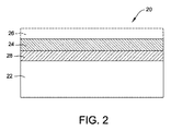
RF系デバイス(例えば、アンテナとスイッチ)用の高抵抗率セミコンダクタ・オン・インシュレータ(例えば、シリコン・オン・インシュレータ)ウエハを利用することにより、コストと集積性の点で、従来の基板に対して有利な効果が得られる。高周波用途で導電性基板を用いたときに本質的に生じる寄生電力損失を低減し、かつ高調波歪を最小化するために、これで十分ではないが、抵抗率の高い基板ウエハを用いることが必要である。したがって、RFデバイス用支持ウエハの抵抗率は、約500Ohm−cmより高いのが一般的である。図1を参照して、シリコン・オン・インシュレータ構造2は、抵抗率の非常に高いシリコンウエハ4、埋め込み酸化物(BOX)層6およびシリコンデバイス層10を備えている。こうした基板は、自由キャリア(電子またはホール)を生成するBOX/支持基板界面の位置に導電性の高い反転層または蓄積層12を形成しやすい。これにより、デバイスがRF周波数で動作するときには、基板の実効抵抗が低下すると共に、寄生電力損失とデバイスの非線形性が生じる。これらの反転層/蓄積層は、BOXに固定された電荷、酸化物にトラップされた電荷、界面にトラップされた電荷、さらに、デバイス自身に印加されたDCバイアスに起因して生じるものである可能性がある。
The use of high resistivity semiconductor-on-insulator (eg, silicon-on-insulator) wafers for RF-based devices (eg, antennas and switches), compared to conventional substrates in terms of cost and integration. An advantageous effect is obtained. To use a high resistivity substrate wafer, although this is not sufficient, to reduce parasitic power losses that are inherently generated when using conductive substrates in high frequency applications and to minimize harmonic distortion is necessary. Therefore, the resistivity of the support wafer for RF devices is generally higher than about 500 Ohm-cm. Referring to FIG. 1, a silicon-on-insulator structure 2 comprises a silicon wafer 4 having a very high resistivity, a buried oxide (BOX) layer 6 and a
それゆえ、非常に近い表面領域であっても基板の高い抵抗率が維持されるように、誘起された反転層または蓄積層において電荷をトラップする方法が必要とされている。高抵抗率支持基板と埋め込み酸化物(BOX)との間に電荷トラップ層(CTL)を設けることにより、SOIウエハを用いたRFデバイスの性能が向上することが知られている。界面トラップ性の高いこれらの層を形成する方法が幾つか提案されている。例えば、図2を参照して、RFデバイス用のCTLを有するセミコンダクタ・オン・インシュレータ20(例えば、シリコン・オン・インシュレータまたはSOI)を製造する1つ方法では、高抵抗率シリコン基板22の上にドープされていない多結晶シリコン膜28を堆積させるステップと、その上に、酸化物スタック24と上部シリコン層26とを形成するステップとを実施する。多結晶シリコン層28は、シリコン基板22と埋め込み酸化物層24との間に設けられた高欠陥層として機能する。図2には、シリコン・オン・インシュレータ構造20において高抵抗率基板22と埋め込み酸化物層24との間に設けられ、電荷トラップ層28として利用される多結晶シリコン膜が示されている。他の方法では、重イオンを注入して、表面付近にダメージ層を形成する。デバイス(例えば、高周波デバイス)は、上部シリコン層26内に形成される。
Therefore, there is a need for a method of trapping charge in the induced inversion or storage layer so that the high resistivity of the substrate is maintained even at very close surface areas. It is known that providing a charge trapping layer (CTL) between a high resistivity support substrate and a buried oxide (BOX) will improve the performance of RF devices using SOI wafers. Several methods for forming these layers with high interface trapping properties have been proposed. For example, referring to FIG. 2, in one method of manufacturing a semiconductor-on-insulator 20 (eg, silicon-on-insulator or SOI) having a CTL for an RF device, on a high resistivity silicon substrate 22 The steps of depositing an undoped
アカデミックな研究によれば、酸化物と基板との間に多結晶シリコン層を設けることにより、デバイスの絶縁性が向上し、伝送線路の損失が低減し、さらに高調波歪みが低減する(例えば、非特許文献1−5を参照)。 According to academic research, by providing a polycrystalline silicon layer between the oxide and the substrate, the insulation of the device is improved, the loss of the transmission line is reduced, and the harmonic distortion is reduced (for example, See Non-Patent Documents 1-5).
簡潔に言って、本発明は、多層構造を準備する方法に関する。
前記方法は、
単結晶半導体支持基板(または単結晶半導体ハンドル基板)のおもて面に界面接触する半導体酸化物層、半導体窒化物層、または半導体酸窒化物層を形成するステップを含み、
前記単結晶半導体支持基板は、互いに略平行な表面である2つの主面を有し、該2つの主面のうち一方は前記単結晶半導体支持基板のおもて面(前面)であり、他方は前記単結晶半導体支持基板の裏面(後面)であり、前記単結晶半導体支持基板は、さらに、前記単結晶半導体支持基板のおもて面と裏面とを接続する周縁部と、前記単結晶半導体支持基板のおもて面と裏面との間に位置する中央平面と、前記単結晶半導体支持基板のおもて面と裏面との間に位置するバルク領域とを有し、前記単結晶半導体支持基板の最小バルク領域抵抗率は、500ohm−cm以上であり、
前記方法は、
前記半導体酸化物層、前記半導体窒化物層、または前記半導体酸窒化物層がおもて面に界面接触している前記単結晶半導体支持基板を、水素、塩化水素、塩素およびこれらの任意の組み合わせから成る群から選択されるガスを含む周囲雰囲気内でアニールするステップと、
前記単結晶半導体支持基板のおもて面に界面接触している半導体酸化物層、半導体窒化物層、または半導体酸窒化物層の上に、多結晶シリコン層を化学気相成長法により堆積させるステップと、
単結晶半導体ドナー基板のおもて面の上に位置する誘電体層を、前記単結晶半導体支持基板の多結晶シリコン層に接合させ、これにより接合構造を形成するステップとを含み、
前記単結晶半導体ドナー基板は、互いに略平行な表面である2つの主面を有し、該2つの主面のうち一方は前記単結晶半導体ドナー基板のおもて面(前面)であり、他方は前記単結晶半導体ドナー基板の裏面(後面)であり、前記単結晶半導体ドナー基板は、さらに、前記単結晶半導体ドナー基板のおもて面と裏面とを接続する周縁部と、前記単結晶半導体ドナー基板のおもて面と裏面との間に位置する中央平面とを有する。
Briefly stated, the present invention relates to a method of preparing a multilayer structure.
The method is
Forming a semiconductor oxide layer, a semiconductor nitride layer, or a semiconductor oxynitride layer in interface contact with the front surface of the single crystal semiconductor support substrate (or the single crystal semiconductor handle substrate);
The single crystal semiconductor supporting substrate has two main surfaces which are surfaces substantially parallel to each other, and one of the two main surfaces is the front surface (front surface) of the single crystal semiconductor supporting substrate, and the other is Is the back surface (rear surface) of the single crystal semiconductor support substrate, and the single crystal semiconductor support substrate further includes a peripheral portion connecting the front surface and the back surface of the single crystal semiconductor support substrate, and the single crystal semiconductor And a bulk region located between the front surface and the back surface of the single crystal semiconductor support substrate, wherein the single crystal semiconductor support is provided with a central plane located between the front surface and the back surface of the support substrate. The minimum bulk area resistivity of the substrate is greater than 500 ohm-cm,
The method is
The semiconductor oxide layer, the semiconductor nitride layer, or the single crystal semiconductor supporting substrate in which the semiconductor oxynitride layer is in interfacial contact with the front surface, hydrogen, hydrogen chloride, chlorine, and any combination thereof Annealing in an ambient atmosphere comprising a gas selected from the group consisting of
A polycrystalline silicon layer is deposited by chemical vapor deposition on the semiconductor oxide layer, the semiconductor nitride layer, or the semiconductor oxynitride layer in interface contact with the front surface of the single crystal semiconductor supporting substrate. Step and
Bonding the dielectric layer located on the front surface of the single crystal semiconductor donor substrate to the polycrystalline silicon layer of the single crystal semiconductor supporting substrate to thereby form a bonding structure.
The single crystal semiconductor donor substrate has two main surfaces which are surfaces substantially parallel to each other, and one of the two main surfaces is the front surface (front surface) of the single crystal semiconductor donor substrate, and the other is Is the back surface (rear surface) of the single crystal semiconductor donor substrate, and the single crystal semiconductor donor substrate further includes a peripheral portion connecting the front surface and the back surface of the single crystal semiconductor donor substrate, and the single crystal semiconductor It has a central plane located between the front and back surfaces of the donor substrate.
本発明は、更なる多層構造を準備する方法に関する。
前記方法は、
単結晶半導体支持基板のおもて面に界面接触する半導体酸化物層、半導体窒化物層、または半導体酸窒化物層を形成するステップを含み、
前記単結晶半導体支持基板は、互いに略平行な表面である2つの主面を有し、該2つの主面のうち一方は前記単結晶半導体支持基板のおもて面であり、他方は前記単結晶半導体支持基板の裏面であり、前記単結晶半導体支持基板は、さらに、前記単結晶半導体支持基板のおもて面と裏面とを接続する周縁部と、前記単結晶半導体支持基板のおもて面と裏面との間に位置する中央平面と、前記単結晶半導体支持基板のおもて面と裏面との間に位置するバルク領域とを有し、前記単結晶半導体支持基板の最小バルク領域抵抗率は、500ohm−cm以上であり、
前記方法は、
前記半導体酸化物層、前記半導体窒化物層、または前記半導体酸窒化物層がおもて面に界面接触している前記単結晶半導体支持基板を、水素、塩化水素、塩素およびこれらの任意の組み合わせから成る群から選択されるガスを含む周囲雰囲気内でアニールするステップと、
前記半導体酸化物層、前記半導体窒化物層、または前記半導体酸窒化物層がおもて面に界面接触している前記単結晶半導体支持基板を、シリコン前駆体を含む約850℃以上の周囲雰囲気に曝露し、前記半導体酸化物層、前記半導体窒化物層、または前記半導体酸窒化物層の上に多結晶シリコン層を堆積させるステップと、
単結晶半導体ドナー基板のおもて面の上に位置する誘電体層を、前記単結晶半導体支持基板の多結晶シリコン層に接合させ、これにより接合構造を形成するステップとを含み、
前記単結晶半導体ドナー基板は、互いに略平行な表面である2つの主面を有し、該2つの主面のうち一方は前記単結晶半導体ドナー基板のおもて面であり、他方は前記単結晶半導体ドナー基板の裏面であり、前記単結晶半導体ドナー基板は、さらに、前記単結晶半導体ドナー基板のおもて面と裏面とを接続する周縁部と、前記単結晶半導体ドナー基板のおもて面と裏面との間に位置する中央平面とを有する。
The present invention relates to a method of preparing further multilayer structures.
The method is
Forming a semiconductor oxide layer, a semiconductor nitride layer, or a semiconductor oxynitride layer in interfacial contact with the front surface of the single crystal semiconductor supporting substrate,
The single crystal semiconductor support substrate has two main surfaces which are surfaces substantially parallel to each other, and one of the two main surfaces is the front surface of the single crystal semiconductor support substrate, and the other is the single surface. A back surface of a crystal semiconductor support substrate, wherein the single crystal semiconductor support substrate further includes a peripheral portion connecting a front surface and a back surface of the single crystal semiconductor support substrate, and a front surface of the single crystal semiconductor support substrate. And a bulk region located between the front surface and the back surface of the single crystal semiconductor support substrate, and having a minimum bulk region resistance of the single crystal semiconductor support substrate. The rate is over 500 ohm-cm,
The method is
The semiconductor oxide layer, the semiconductor nitride layer, or the single crystal semiconductor supporting substrate in which the semiconductor oxynitride layer is in interfacial contact with the front surface, hydrogen, hydrogen chloride, chlorine, and any combination thereof Annealing in an ambient atmosphere comprising a gas selected from the group consisting of
An ambient atmosphere including a silicon precursor and the single crystal semiconductor supporting substrate in which the semiconductor oxide layer, the semiconductor nitride layer, or the semiconductor oxynitride layer is in interfacial contact with the front surface, and which includes a silicon precursor And exposing a polycrystalline silicon layer on the semiconductor oxide layer, the semiconductor nitride layer, or the semiconductor oxynitride layer;
Bonding the dielectric layer located on the front surface of the single crystal semiconductor donor substrate to the polycrystalline silicon layer of the single crystal semiconductor supporting substrate to thereby form a bonding structure.
The single crystal semiconductor donor substrate has two main surfaces which are surfaces substantially parallel to each other, one of the two main surfaces is the front surface of the single crystal semiconductor donor substrate, and the other is the single surface. A back surface of a crystalline semiconductor donor substrate, wherein the single crystal semiconductor donor substrate further includes a peripheral portion connecting a front surface and a back surface of the single crystal semiconductor donor substrate, and a front surface of the single crystal semiconductor donor substrate. It has a central plane located between the face and the back.
本発明は、さらに、多層構造に関する。
前記多層構造は、単結晶半導体支持基板を備え、
前記単結晶半導体支持基板は、互いに略平行な表面である2つの主面を有し、該2つの主面のうち一方は前記単結晶半導体支持基板のおもて面であり、他方は前記単結晶半導体支持基板の裏面であり、前記単結晶半導体支持基板は、さらに、前記単結晶半導体支持基板のおもて面と裏面とを接続する周縁部と、前記単結晶半導体支持基板のおもて面と裏面との間に位置する中央平面と、前記単結晶半導体支持基板のおもて面と裏面との間に位置するバルク領域とを有し、前記単結晶半導体支持基板の最小バルク領域抵抗率は、500ohm−cm以上であり、
前記多層構造は、
前記単結晶半導体支持基板のおもて面に界面接触し、約5ナノメートル以上約1000ナノメートル以下の大きさの穴を有する、凹凸のある半導体酸化物層、凹凸のある半導体酸化物層または凹凸のある半導体酸窒化物層と、
前記凹凸のある半導体酸化物層、前記凹凸のある半導体酸化物層または前記凹凸のある半導体酸窒化物層に界面接触している多結晶シリコン層と、
前記多結晶シリコン層に界面接触している誘電体層と、
前記誘電体層と界面接触している単結晶半導体デバイス層と、をさらに備え、
前記多層構造のウエハバウは、前記半導体デバイス層のおもて面、および/または、前記単結晶半導体支持基板の裏面の少なくとも3点で測定して、約80マイクロメートルより小さい。
The invention further relates to a multilayer structure.
The multilayer structure comprises a single crystal semiconductor support substrate,
The single crystal semiconductor support substrate has two main surfaces which are surfaces substantially parallel to each other, and one of the two main surfaces is the front surface of the single crystal semiconductor support substrate, and the other is the single surface. A back surface of a crystal semiconductor support substrate, wherein the single crystal semiconductor support substrate further includes a peripheral portion connecting a front surface and a back surface of the single crystal semiconductor support substrate, and a front surface of the single crystal semiconductor support substrate. And a bulk region located between the front surface and the back surface of the single crystal semiconductor support substrate, and having a minimum bulk region resistance of the single crystal semiconductor support substrate. The rate is over 500 ohm-cm,
The multilayer structure is
An uneven semiconductor oxide layer, an uneven semiconductor oxide layer or an uneven semiconductor oxide layer having an interface contact with the front surface of the single crystal semiconductor supporting substrate and having a hole size of about 5 nm or more and about 1000 nm or less An uneven semiconductor oxynitride layer,
A polycrystalline silicon layer interface-contacted with the uneven semiconductor oxide layer, the uneven semiconductor oxide layer, or the uneven semiconductor oxynitride layer;
A dielectric layer interfaced with the polycrystalline silicon layer;
Further comprising a single crystal semiconductor device layer in interface contact with the dielectric layer;
The wafer bow of the multilayer structure is less than about 80 micrometers, as measured at at least three points on the front surface of the semiconductor device layer and / or the back surface of the single crystal semiconductor support substrate.
本発明の他の課題と特徴の一部は、以下の説明により明らかになり、また、以下の説明で指摘している。 Other objects and features of the present invention will become apparent in the following description and are pointed out in the following description.
本発明によれば、単結晶半導体支持基板(例えば、単結晶半導体支持ウエハ)の上に電荷トラップ層を製造するための方法が提供される。電荷トラップ層を備えた単結晶半導体支持ウエハ(または単結晶半導体ハンドルウエハ)は、セミコンダクタ・オン・インシュレータ(例えば、シリコン・オン・インシュレータ)構造の製造において有用である。本発明によれば、単結晶半導体支持ウエハにおける電荷トラップ層は、セミコンダクタ・オン・インシュレータ構造における酸化物界面付近(つまり、埋め込み酸化物層またはBOX付近)の領域に形成される。好都合には、本発明の方法によれば、熱処理(例えば、後で説明するセミコンダクタ・オン・インシュレータ基板とデバイスの製造における熱処理ステップ)に対して安定性の高い高欠陥の電荷トラップ層が得られる。好都合には、本発明の方法によれば、電荷トラップ層を準備する従来の手法を用いた場合と比較して汚染物質が少ない清浄な多結晶シリコン電荷トラップ層が得られる。好都合には、本発明の方法によれば、ワープとバウが低減した支持基板を備えたセミコンダクタ・オン・インシュレータ構造が得られる。 According to the present invention, a method is provided for fabricating a charge trapping layer on a single crystal semiconductor support substrate (eg, a single crystal semiconductor support wafer). Single crystal semiconductor support wafers (or single crystal semiconductor handle wafers) with charge trapping layers are useful in the fabrication of semiconductor-on-insulator (eg, silicon-on-insulator) structures. According to the present invention, the charge trapping layer in the single crystal semiconductor supporting wafer is formed in the region near the oxide interface (that is, near the buried oxide layer or BOX) in the semiconductor-on-insulator structure. Advantageously, according to the method of the present invention, a high defect charge trapping layer is obtained which is highly stable to heat treatment (e.g. a heat treatment step in the manufacture of semiconductor-on-insulator substrates and devices described later). . Advantageously, the method of the present invention results in a clean polycrystalline silicon charge trapping layer with less contamination compared to using conventional techniques for preparing a charge trapping layer. Advantageously, the method of the present invention provides a semiconductor-on-insulator structure with a support substrate with reduced warp and bow.
本発明の方法に従って準備した支持基板は、セミコンダクタ・オン・インシュレータ (例えばシリコン・オン・インシュレータ)構造の製造での利用に適している。ここで、図3を参照する。公知技術により層を転写し、少なくとも、以下の層または領域、つまり、支持基板42、半導体酸化物層44、電荷トラップ層46、誘電体層48(例えば、埋め込み酸化物)および単結晶半導体デバイス層50(例えば、単結晶シリコンドナー基板から得られるシリコン層)、を備えた本発明のセミコンダクタ・オン・インシュレータ(例えば、シリコン・オン・インシュレータ)構造40を作る。幾つかの実施形態では、本発明のセミコンダクタ・オン・インシュレータ (例えば、シリコン・オン・インシュレータ)構造40は、少なくとも、以下の層または領域、つまり、支持基板42、半導体窒化物または半導体酸窒化物層44、電荷トラップ層46、誘電体層48(例えば、埋め込み酸化物)および単結晶半導体デバイス層50(例えば、単結晶シリコンドナー基板から得られるシリコン層)を備えている。
The support substrate prepared in accordance with the method of the present invention is suitable for use in the manufacture of semiconductor-on-insulator (eg, silicon-on-insulator) structures. Here, FIG. 3 is referred to. Transfer layers by known techniques and at least the following layers or regions:
本発明の方法と構造で用いられる基板は、半導体支持基板42(例えば、単結晶半導体支持ウエハ)および半導体ドナー基板(例えば、単結晶半導体ドナーウエハ)であってもよい。セミコンダクタ・オン・インシュレータ複合材構造40における半導体デバイス層50は、単結晶半導体ドナーウエハから得られる。半導体デバイス層50は、例えば半導体ドナー基板をエッチングするウエハシンニング技術、または損傷した平面を有する半導体ドナー基板の割断により、半導体支持基板42の上に転写してよい。概して、単結晶半導体支持ウエハおよび単結晶半導体ドナーウエハは、略平行な2つの主面を有している。一方の平行な面は基板のおもて面であり、他方の平行な面は基板の裏面である。基板は、おもて面と裏面とを接続する周縁部、おもて面と裏面の間に位置するバルク領域、および、おもて面と裏面との間に位置する中央平面とを有している。基板は、さらに、中央平面に対して垂直な仮想中心軸と、仮想中心軸から周縁部までの径方向長さを有する。さらに、半導体基板(例えば、シリコンウエハ)は、典型的には、所定の大きさの全体厚みムラ(TTV:total thickness variation)、ワープ(warp)およびバウ(bow)を有しているので、おもて面上の点と裏面上の点との中点が常に正確に平面内にあるとは限らない。ただし、実際上、TTV、ワープおよびバウの大きさは、典型的には非常に小さいとみなすことができ、中点群は、おもて面と裏面から略等距離の位置にある仮想中央面内に入るということができる。
The substrates used in the methods and structures of the present invention may be a semiconductor support substrate 42 (e.g., a single crystal semiconductor support wafer) and a semiconductor donor substrate (e.g., a single crystal semiconductor donor wafer). The
本明細書で説明しているいずれかの操作の前に、基板のおもて面と裏面は実質的に同一であってよい。表面を「おもて面」、「裏面」と称しているのは、便宜上、単に本発明の方法による操作を行う表面を区別するためである。本発明では、単結晶半導体支持基板(例えば、単結晶シリコン支持ウエハ)の「おもて面」は、基板の主面であって接合構造の内面となる面を指す。図3を参照して、本発明の電荷トラップ層46は、半導体酸化物層44との界面接触部に形成されている。半導体酸化物層44は、単結晶半導体支持基板42のおもて面に形成されている。単結晶半導体支持基板42(例えば、支持ウエハ)の「裏面(rear surface)」は、主面であってセミコンダクタ・オン・インシュレータ複合材(コンポジット)構造40の外表面となる面を指す。同様に、単結晶半導体ドナー基板(例えば、単結晶シリコンドナーウエハ)の「おもて面(front surface)」は、単結晶半導体ドナー基板の主面であって、セミコンダクタ・オン・インシュレータ複合材構造40の内表面を構成するものを指す。単結晶半導体ドナー基板のおもて面には、しばしば誘電体層(例えば、二酸化ケイ素層)が設けられる。この誘電体層は、最終構造において埋め込み酸化物(BOX)層を構成する。単結晶半導体ドナー基板(例えば、単結晶シリコンドナーウエハ)の「裏面」は、単結晶半導体ドナー基板の主面であって、セミコンダクタ・オン・インシュレータ複合材構造40の外表面を構成するものを指す。従来の接合ステップおよびウエハシンニングステップを完了すると、単結晶半導体ドナー基板により、複合材構造40を含むセミコンダクタ・オン・インシュレータ(例えば、シリコン・オン・インシュレータ)の半導体デバイス層50が形成される。
Prior to any of the operations described herein, the front and back surfaces of the substrate may be substantially identical. The front side is referred to as "front side" and "back side", for the sake of convenience, merely to distinguish the surface on which the method according to the invention is operated. In the present invention, the “front surface” of a single crystal semiconductor support substrate (for example, a single crystal silicon support wafer) refers to the main surface of the substrate and the inner surface of the bonding structure. Referring to FIG. 3, the charge trapping layer 46 of the present invention is formed at the interface contact with the semiconductor oxide layer 44. The semiconductor oxide layer 44 is formed on the front surface of the single crystal
半導体支持基板42とデバイス層50は、単結晶半導体材料を含んでいてよい。好ましい実施形態では、半導体材料は、シリコン、炭化ケイ素、サファイア、窒化アルミニウム、シリコンゲルマニウム、ガリウムヒ素、窒化ガリウム、リン化インジウム、インジウムガリウムヒ素、ゲルマニウム、およびこれらの組み合わせから成る群から選択されてよい。半導体支持基板42およびデバイス層46は、互いに同じ半導体材料を含んでいてもよいし、互いに異なる半導体材料を含んでいてもよい。したがって、セミコンダクタ・オン・インシュレータ複合材構造40は、例えば、シリコン・オン・インシュレータ、サファイア・オン・インシュレータ、窒化アルミニウム・オン・インシュレータおよびその他の組み合わせであってもよい。本発明の単結晶半導体ウエハ(例えば、単結晶シリコン支持ウエハと単結晶シリコンドナーウエハ)の公称径は、典型的には、約150mm以上、約200mm以上、約300mm以上、または約450mm以上である。ウエハの厚みは、約250マイクロメートル以上約1500マイクロメートル以下、例えば、約300マイクロメートル以上約1000マイクロメートル以下、好適には約500マイクロメートル以上約1000マイクロメートル以下であってよい。幾つかの具体的な実施形態では、ウエハの厚みは約725マイクロメートルであってもよい。
The
特に好ましい実施形態では、単結晶半導体ウエハの例は、従来のチョクラルスキー結晶成長法またはフロートゾーン成長法に従って成長した単結晶インゴットから切り出された単結晶シリコンウエハである。当該方法、および、標準のシリコンスライス、ラップ、エッチングおよび研磨は、例えば、F. Shimura, Semiconductor Silicon Crystal Technology, Academic Press, 1989, and Silicon Chemical Etching, (J. Grabmaier ed.) Springer-Verlag, N.Y., 1982に開示されている(この文献は、参照により本明細書に組み込まれる)。好ましくは、ウエハは、当業者に知られた標準的な方法により研磨および洗浄される(例えば、W.C. O’Mara et al., Handbook of Semiconductor Silicon Technology, Noyes Publicationsを参照)。必要であれば、ウエハは、例えば、標準的なSC1/SC2溶液を用いて洗浄してもよい。幾つかの実施形態では、本発明の単結晶シリコンウエハは、従来のチョクラルスキー(Cz)結晶成長法に従って成長した単結晶インゴットから切り出されたものであり、典型的な公称径は、約150nm以上、約200nm以上、約300nm以上、または約450nm以上である。好ましくは、単結晶シリコン支持ウエハと単結晶シリコンドナーウエハの両方が、鏡面研磨されたおもて面の仕上がりを有しており、表面欠陥(スクラッチ、大径のパーティクルなど)がない。ウエハの厚みは、約250マイクロメートル以上約1500マイクロメートル以下(例えば、約300マイクロメートル以上約1000マイクロメートル以下)、好適には、約500マイクロメートル以上約1000マイクロメートル以下であってよい。ある具体的な実施形態では、ウエハの厚みは約725マイクロメートルであってもよい。 In a particularly preferred embodiment, an example of a single crystal semiconductor wafer is a single crystal silicon wafer cut from a single crystal ingot grown according to the conventional Czochralski crystal growth method or float zone growth method. The method and standard silicon slices, wraps, etching and polishing are described, for example, in F. Shimura, Semiconductor Silicon Crystal Technology, Academic Press, 1989, and Silicon Chemical Etching, (J. Grabmaier ed.) Springer-Verlag, NY , 1982, which is incorporated herein by reference. Preferably, the wafer is polished and cleaned by standard methods known to those skilled in the art (see, for example, W.C. O'Mara et al., Handbook of Semiconductor Silicon Technology, Noyes Publications). If necessary, the wafer may be cleaned using, for example, a standard SC1 / SC2 solution. In some embodiments, the single crystal silicon wafer of the present invention is cut from a single crystal ingot grown according to conventional Czochralski (Cz) crystal growth method, and has a typical nominal diameter of about 150 nm Or more, about 200 nm or more, about 300 nm or more, or about 450 nm or more. Preferably, both the single crystal silicon support wafer and the single crystal silicon donor wafer have a mirror-polished front surface finish and are free of surface defects (scratch, large diameter particles, etc.). The thickness of the wafer may be about 250 micrometers or more and about 1500 micrometers or less (e.g., about 300 micrometers or more and about 1000 micrometers or less), preferably about 500 micrometers or more and about 1000 micrometers or less. In one specific embodiment, the thickness of the wafer may be about 725 micrometers.
幾つかの実施形態では、単結晶半導体支持基板および単結晶半導体ドナー基板(つまり、単結晶半導体支持ウエハおよび単結晶半導体ドナーウエハ)は、一般的にチョクラルスキー成長法で達成される濃度で格子間酸素を含んでいる。幾つかの実施形態では、約4ppma以上約18ppma以下の濃度で酸素を含んでいる。幾つかの実施形態では、約10ppma以上約35ppma下の濃度で酸素を含んでいる。好ましくは、単結晶シリコン支持ウエハは、約10ppma以下の濃度で酸素を含んでいる。格子間酸素は、SEMI MF 1188−1105を用いて測定してよい。 In some embodiments, a single crystal semiconductor support substrate and a single crystal semiconductor donor substrate (ie, a single crystal semiconductor support wafer and a single crystal semiconductor donor wafer) are generally interstitially grown at concentrations achieved by Czochralski growth. Contains oxygen. Some embodiments include oxygen at a concentration of about 4 to about 18 ppma. Some embodiments include oxygen at a concentration of about 10 ppma or more and about 35 ppma or less. Preferably, the single crystal silicon support wafer contains oxygen at a concentration of about 10 ppma or less. Interstitial oxygen may be measured using SEMI MF 1188-1105.
図3を参照して、幾つかの実施形態では、単結晶半導体支持基板42(例えば、単結晶シリコン支持ウエハ)の最小バルク抵抗率は、比較的高い。高抵抗率ウエハは、一般的に、チョクラルスキー法またはフロートゾーン法により成長した単結晶インゴットから切り出す。高抵抗率ウエハは、電気的に活性なドーパント、例えばホウ素(p型)、ガリウム(p型)、リン(n型)、アンチモン(n型)およびヒ素(n型)を、概して非常に低い濃度で含んでいてよい。Cz法により成長したシリコンウエハには、約600℃以上約1000℃以下の温度でアニールを実施し、結晶成長中に取り込まれた酸素により生じる熱ドナーをなくす。幾つかの実施形態では、単結晶半導体支持ウエハの最小バルク抵抗率は、100Ohm−cm以上、または、500Ohm−cm以上であり、例えば約100Ohm−cm以上約100,000Ohm−cm以下、または約500Ohm−cm以上約100000Ohm−cm以下、または、約1000Ohm−cm以上約100000Ohm−cm以下、または、約500Ohm−cm以上約10000Ohm−cm以下、または、約750Ohm−cm以上約10000Ohm−cm以下、約1000Ohm−cm以上約10000Ohm−cm以下、約200Ohm−cm以上約10000Ohm−cm以下、約300Ohm−cm以上約10000Ohm−cm以下、または、約300Ohm−cm以上約5000Ohm−cm以下である。高抵抗率ウエハを準備する方法は、この技術分野では知られており、SunEdison,Inc.(ミズーリ州セントピーターズ、以前はMEMC Electronic Materials,Inc.)などのサプライヤーから入手できる。 Referring to FIG. 3, in some embodiments, the minimum bulk resistivity of single crystal semiconductor support substrate 42 (eg, a single crystal silicon support wafer) is relatively high. High resistivity wafers are generally cut from single crystal ingots grown by the Czochralski method or the float zone method. High resistivity wafers generally have very low concentrations of electrically active dopants such as boron (p-type), gallium (p-type), phosphorus (n-type), antimony (n-type) and arsenic (n-type) May be included. The silicon wafer grown by the Cz method is annealed at a temperature of about 600 ° C. or more and about 1000 ° C. or less to eliminate the thermal donor generated by oxygen taken in during crystal growth. In some embodiments, the minimum bulk resistivity of the single crystal semiconductor support wafer is greater than or equal to 100 Ohm-cm, or greater than or equal to 500 Ohm-cm, such as greater than or equal to about 100 Ohm-cm and less than or equal to about 100,000 Ohm-cm, or about 500 Ohm. -Cm to about 100,000 ohm-cm or less, or about 1000 ohm-cm to about 100,000 ohm-cm or less, or about 500 ohm-cm to about 10,000 ohm-cm or less, or about 750 ohm-cm to about 10,000 ohm-cm or less, about 1000 ohm -Cm to about 10000 Ohm-cm or less, about 200 Ohm-cm to about 10000 Ohm-cm or less, about 300 Ohm-cm to about 10000 Ohm-cm or less, or about 300 Ohm-cm to about 5000 Ohm-cm or less A. Methods for preparing high resistivity wafers are known in the art and can be found in Sun Edison, Inc. Available from suppliers such as (St. Peters, MO, formerly MEMC Electronic Materials, Inc.).
幾つかの実施形態では、高抵抗単結晶半導体支持基板42は、p型ドーパントまたはn型ドーパントを含んでいる。好適なドーパントの例は、ホウ素(p型)、ガリウム(p型)、リン(n型)、ヒ素(n型)である。幾つかの実施形態では、単結晶半導体支持基板は、p型ドーパントを含んでいる。幾つかの実施形態では、単結晶半導体支持基板は、p型ドーパント(例えばホウ素)を含む単結晶シリコンウエハである。ホウ素ドーパントの濃度は、高抵抗率支持基板を得ることができるように、比較的低く、例えば1×10¹⁴atoms/cm3未満、好ましくは1×1013atoms/cm3未満である。
In some embodiments, the high resistance single crystal
幾つかの実施形態では、単結晶半導体支持基板42(例えば、単結晶シリコン支持ウエハ)の最小バルク抵抗率は比較的低く、例えば、約100ohm−cm未満、約50ohm−cm未満、約1ohm−cm未満、約0.1ohm−cm未満または約0.01ohm−cm未満である。幾つかの好ましい実施形態では、単結晶半導体支持基板42の最小バルク抵抗率は比較的低く、例えば、約100ohm−cm未満、または、約1ohm−cm以上約100ohm−cm以下である。低抵抗率ウエハは、電気的に活性なドーパント、例えばホウ素(p型)、ガリウム(p型)、リン(n型)、アンチモン(n型)およびヒ素(n型)を含んでいてもよい。
In some embodiments, the minimum bulk resistivity of the single crystal semiconductor support substrate 42 (eg, a single crystal silicon support wafer) is relatively low, eg, less than about 100 ohm-cm, less than about 50 ohm-cm, about 1 ohm-cm Less than about 0.1 ohm-cm or less than about 0.01 ohm-cm. In some preferred embodiments, the minimum bulk resistivity of the single crystal
幾つかの実施形態では、サウンドブラスティング(sound blasting)プロセスまたはコースティックエッチング(caustic etch)により、単結晶半導体支持基板42の表面に意図的にダメージを与えてもよい。
In some embodiments, the surface of the single crystal
本発明の方法に従って、単結晶半導体支持基板42のおもて面は、例えば酸化性媒質に曝露することにより、酸化してよい。単結晶半導体支持基板42を酸化することにより、支持基板42のおもて面に半導体酸化物層44が形成される。幾つかの実施形態では、単結晶半導体支持基板42のおもて面は、半導体窒化物層または半導体酸窒化物層を含んでいてよい。幾つかの実施形態では、単結晶半導体支持基板42は、空気またはオゾンに曝露してもよい。幾つかの実施形態では、単結晶半導体支持基板42は、酸化剤を含む水溶液に浸漬してもよい。当該水溶液の例は、SC1溶液である。幾つかの実施形態では、単結晶半導体支持基板42は、電荷トラップ層を堆積させる前に、熱酸化(これにより、単結晶半導体材料が幾らか消費されることになる)、および/または、CVD酸化物成長、および/または、原子層堆積により酸化してもよい。
According to the method of the present invention, the front surface of the single crystal
幾つかの実施形態では、単結晶半導体支持基板42のおもて面に、所定のプロセス(例えば酸化プロセス)を施し、これにより誘電体層(例えば、半導体酸化物層、半導体窒化物層または半導体酸窒化物層)を成長させてもよい。幾つかの実施形態では、誘電体層は二酸化ケイ素を含んでいる。二酸化ケイ素は、シリコン支持基板のおもて面を酸化することにより形成できる。おもて面の酸化は、熱酸化(これにより、堆積した半導体材料膜が幾らか消費されることになる)、および/または、CVD酸化物成長、および/または、原子層堆積により行ってよい。幾つかの実施形態では、半導体支持基板は、加熱炉(例えば、ASM A400)内で熱酸化してもよい。このときの温度は、酸化環境において750℃以上1100℃以下であってよい。酸化環境雰囲気は、不活性ガス(例えばArまたはN2)とO2との混合物であってよい。酸素含有量は、1%以上10%以下、またはそれ以上であってよい。幾つかの実施形態では、酸化環境雰囲気は、最大酸素100%(ドライ酸化)であってもよい。幾つかの実施形態では、酸化環境雰囲気は、酸素とアンモニアを含んでいてもよい。幾つかの実施形態では、環境雰囲気は、不活性ガス(例えば、ArまたはN2)と酸化性ガス(例えば、O2と水蒸気(ウェット酸化))の混合物を含んでいてもよい。幾つかの実施形態では、環境雰囲気は、不活性ガス(例えば、ArまたはN2)と酸化性ガス(例えば、O2と水蒸気(ウェット酸化))と窒化性ガス(例えば、アンモニア)を含んでいてもよい。幾つかの実施形態では、環境雰囲気は、不活性ガス(例えば、ArまたはN2)と窒化性ガス(例えば、アンモニア)を含んでいてもよい。例示的な実施形態では、半導体支持ウエハは、垂直炉(例えば、A400)内でロードしてもよい。温度は、N2とO2の混合物を用いた酸化温度まで上昇させる。所望の温度で、水蒸気をガス流内へ導入する。所望の酸化物の厚みを得た後、水蒸気とO2の供給を止め、加熱炉の温度を低下させ、ウエハを加熱炉からアンロードする。
In some embodiments, the front surface of the single crystal
幾つかの実施形態では、支持基板42は、酸化剤を含む水溶液(例えば、SC1溶液またはSC2溶液)に浸漬することにより酸化してよい。幾つかの実施形態では、SC1溶液は、脱イオン水を5部、水性のNH4OH(水酸化アンモニウム、NH3は重量パーセント濃度で29%)を1部、水性のH2O2を1部(過酸化水素、30%)含んでいる。幾つかの実施形態では、支持基板は、酸化剤を含む水溶液(例えば、SC2溶液)に浸漬することにより酸化してよい。幾つかの実施形態では、SC2溶液は、脱イオン水を5部、水性のHCl(塩化水素、39%)を1部、水性のH2O2(過酸化水素、30%)を1部含んでいる。
In some embodiments, the
幾つかの実施形態では、支持基板42は酸化され、基板42のおもて面層との界面接触部に、厚みが約0.1ナノメートル以上約25ナノメートル以下(例えば約0.5ナノメートル以上約5ナノメートル以下、または、約1ナノメートル以上約5ナノメートル以下)の半導体酸化物層44が設けられる。
In some embodiments,
単結晶半導体支持基板42のおもて面を酸化して当該おもて面に半導体酸化物層44を形成した後、おもて面に半導体酸化物層44が設けられた単結晶半導体支持基板42を、還元剤および/またはエッチング剤を含む周囲雰囲気に曝露する。還元剤および/またはエッチング剤を含む周囲雰囲気に曝露することにより、好都合には基板の上にある酸化物層が清浄化され、後で実施する多結晶シリコンの堆積のために半導体酸化物層に凹凸が形成される。クリーンルーム内でのウエハハンドリングにより、有機汚染物質、ホウ素、アルミニウム、リンなどの汚染物質が、支持基板の表面の上に堆積することがある。汚染物質は、多結晶シリコン膜の核形成プロセスを妨害したり、シリコン内で望まないドーパントになったりする。後者の場合、基板や多結晶シリコン膜の抵抗率が変化し、これにより高周波信号の歪みや電力損失が大きくなる。還元剤および/またはエッチング剤を含む周囲雰囲気により、これらの汚染物質を清浄化できる。本発明では、水素などの還元剤が、酸化ホウ素や酸化アルミニウムなど、クリーンルームに一般的に存在する汚染物質と反応する。一方、塩素や塩化水素などのエッチングガスは、アルミニウム、ホウ素およびリンと反応して揮発性の塩素系物質を生成する。この塩素系物質は、水素ガスにより、シリコン表面から取り除かれる。シリコン酸化物が存在すると、有機物である汚染物質中の炭素原子がシリコン原子に置き換わり、一酸化炭素が生成する。この一酸化炭素は、水素キャリアガスにより、シリコン表面から取り除かれる。それゆえ、高純度・高効率の電荷トラップ層を得るためには、多結晶シリコンを堆積させる前にベーキング/エッチングステップを実施することが好都合である。さらに、ベーキング/エッチングプロセスにより、酸化物層内にホールが形成されて凹凸のある酸化物構造が形成され、これにより、多結晶シリコン電荷トラップ層の堆積中に、シリコン表面がシリコン前駆体に対して露出する。凹凸のある酸化物に形成されたホールの密度と大きさは、ベーキング/エッチングステップにおける温度、時間およびガス流量により十分に制御できる。典型的には、ホールの大きさは、約5ナノメートル以上約1000ナノメートル以下、例えば、約5ナノメートル以上約500ナノメートル以下または約5ナノメートル以上約200ナノメートル以下の範囲で制御でき、これにより、多結晶シリコンの粒径および膜応力の設計が可能になる。ここで、図4を参照する。図4は、酸化物内に形成され、多結晶シリコンの電荷トラップ層のための核形成サイトを与える約40nmの開口部を示している。凹凸のある酸化物構造を十分に制御して、酸化物層全体をなくすことなく、ウエハ表面にわたって均一な密度の穴を形成する必要がある。残留酸化物は、多結晶シリコン電荷トラップ層の熱安定性にとって重要である。この後に行う、SOI基板の熱処理およびデバイスの製造において、多結晶シリコン層は、再結晶化を経て多結晶粒と単結晶基板との直接接触により製造されうる。多結晶シリコンと基板との界面に残留している酸化物により、再結晶化プロセスが有効にブロックされ、多結晶シリコン層の、電荷トラップ機能を有しない単結晶シリコンへの変化が妨げられる。
A single crystal semiconductor supporting substrate in which a semiconductor oxide layer 44 is provided on the front surface after the front surface of the single crystal
洗浄/アニールステップは、多結晶シリコン電荷トラップ層を堆積させたのと同じチャンバ(例えば、CVD反応チャンバ)内で実施するのが好都合である。還元雰囲気は、追加的に、ウエハをさらに清浄にするためのエッチャントを含んでいてよい。したがって、ウエハ洗浄用の周囲雰囲気は、水素、塩化水素、塩素、または、水素、塩化水素および塩素の任意の組み合わせを含んでいてよい。幾つかの実施形態では、ウエハ洗浄用の周囲雰囲気は、水素と塩化水素を含んでいてよい。幾つかの実施形態では、ウエハ洗浄用の周囲雰囲気は、水素と塩素を含んでいてよい。さらに、ウエハ洗浄は、高温(例えば、850℃より高い温度、例えば、850℃以上約1100℃以下、または、約850℃以上約1000℃以下、好ましくは900℃以上約1000℃以下)で実施してもよい。チャンバ内の圧力は、大気圧または大気圧よりも低い圧力(例えば、1Torr以上760Torr以下、1Torr以上400Torr以下)であってもよい。洗浄のための所望の温度で、ウエハは、水素、塩化水素、塩素、または、水素、塩化水素および塩素の任意の組み合わせを含む周囲雰囲気に、約1秒以上約300秒以下(例えば、約5秒以上約60秒以下、または、約10秒以上約40秒以下)曝露してよい。 The cleaning / annealing step is conveniently performed in the same chamber (eg, a CVD reaction chamber) in which the polycrystalline silicon charge trap layer is deposited. The reducing atmosphere may additionally include an etchant to further clean the wafer. Thus, the ambient atmosphere for cleaning the wafer may include hydrogen, hydrogen chloride, chlorine, or any combination of hydrogen, hydrogen chloride and chlorine. In some embodiments, the ambient atmosphere for wafer cleaning may include hydrogen and hydrogen chloride. In some embodiments, the ambient atmosphere for wafer cleaning may include hydrogen and chlorine. Furthermore, wafer cleaning is performed at a high temperature (for example, a temperature higher than 850 ° C., for example, 850 ° C. to about 1100 ° C. or about 850 ° C. to about 1000 ° C., preferably 900 ° C. to about 1000 ° C.). May be The pressure in the chamber may be atmospheric pressure or a pressure lower than atmospheric pressure (for example, 1 Torr or more and 760 Torr or less, 1 Torr or more and 400 Torr or less). At a desired temperature for cleaning, the wafer may be in the ambient atmosphere containing hydrogen, hydrogen chloride, chlorine, or any combination of hydrogen, hydrogen chloride and chlorine for about 1 second or more and about 300 seconds or less (e.g., about 5 seconds). Seconds or more and about 60 seconds or less, or about 10 seconds or more and about 40 seconds or less).
単結晶半導体支持基板42のおもて面の上に半導体酸化物層44を形成し、さらにウエハにアニールおよび凹凸形成を行った後、半導体酸化物層44との界面接触部に多結晶シリコン電荷トラップ層46を堆積させる。幾つかの実施形態では、単結晶半導体支持基板42のおもて面の上に設けられた半導体酸化物層44の上に、半導体材料を堆積させる。セミコンダクタ・オン・インシュレータデバイス40の電荷トラップ層46の形成に適した半導体材料は、製造したデバイスにおいて大きな欠陥のある層を形成できる。幾つかの実施形態では、電荷トラップ層は多結晶シリコンを含む。ここでいう多結晶材料は、結晶方位が不規則な小さい結晶を複数含んでいる材料を指す。多結晶粒の粒径は、約20ナノメートルであってもよい。多結晶粒の大きさ(粒径)は、約20ナノメートルであってもよい。粒の大きさは、約20ナノメートル以上約1マイクロメートル以下であってもよく、例えば、約0.3マイクロメートル以上約1マイクロメートル以下であってもよい。本発明の方法によれば、堆積した多結晶材料の結晶粒径が小さいほど、電荷トラップ層における欠陥が大きくなる。多結晶シリコン電荷トラップ層の抵抗率は、100Ohm−cm以上、約500Ohm−cm以上、約1000Ohm−cm以上、または、約3000Ohm−cm以上、例えば、約100Ohm−cm以上約100000Ohm−cm以下、または、約500Ohm−cm以上約100000Ohm−cm以下、または、約1000Ohm−cm以上約100000Ohm−cm以下、約500Ohm−cm以上約10,000Ohm−cm以下、または、約750Ohm−cm以上約10000Ohm−cm以下、約1000Ohm−cm以上約10,000Ohm−cm以下、約2000Ohm−cm以上約10000Ohm−cm以下、約3000Ohm−cm以上約10000Ohm−cm以下、または、約3000Ohm−cm以上約8000Ohm−cm以下であってよい。多結晶シリコンは、有機金属化学気相成長法(MOCVD)、物理気相成長法(PVD)、化学気相成長法(CVD)、低圧化学気相成長法(LPCVD)、プラズマ増強化学気相成長法(PECVD)または分子線エピタキシー(MBE)を用いて堆積させてよい。幾つかの実施形態では、多結晶シリコンは、化学気相成長法により堆積させる。幾つかの実施形態では、多結晶シリコンは、高温で堆積させる。幾つかの実施形態では、多結晶シリコンを堆積させた後、支持基板を高温でアニールする。幾つかの実施形態では、多結晶シリコンの一部を堆積させることにより、電荷トラップ層の最終の厚みと比べて小さい厚みの多結晶シリコンシード層を堆積させる。多結晶シード層を備えた支持基板を高温でアニールし、その後、残りの電荷トラップ層を堆積させる。幾つかの実施形態では、十分に堆積した多結晶シリコン電荷トラップ層を高温でアニールして、膜応力を約0MPa以上約500MPa以下(例えば、約0MPa以上約100MPa以下)まで低下させることができる。半導体酸化物層44により、電荷トラップ層46の高い多結晶性(polycrystallinity)を得やすくなる。したがって、電荷トラップ層46の堆積前に半導体酸化物層44が形成されていない場合、堆積した半導体材料の結晶性は下位の基板42の結晶性に従いやすくなるが、これは電荷トラップ層にとっては好ましくない。
After the semiconductor oxide layer 44 is formed on the front surface of the single-crystal
幾つかの実施形態では、半導体酸化物層は、電荷トラップ層の堆積ステップにおいてエピタキシャルシリコン層の代わりに多結晶シリコン層を形成するために、支持基板の上に存在している。半導体酸化物層の上での多結晶シリコン層の核形成は、H2とHClの一方または両方と、選択的にシリコン前駆体とを含む周囲雰囲気における半導体酸化物層の選択的エッチングにより実現する。エッチングと多結晶シリコン層の堆積はこの順序で実施してよく、このときエッチングステップを最初に、または同時に実施してよい。エッチング周囲雰囲気、または、多結晶シリコンを堆積させるための雰囲気に含まれる例示的なシリコン前駆体は、メチルシラン、四水素化ケイ素(シラン)、トリシラン、ジシラン、ペンタシラン、ネオペンタシラン、テトラシラン、ジクロロシラン(SiH2Cl2)、トリクロロシラン(SiHCl3)、四塩化ケイ素(SiCl4)から選択されてよい。多結晶シリコンの成長は、半導体酸化物層における開口部の形成により開始し、隣接する核どうしが1つになり、成長に伴って硬い膜が形成される。半導体酸化物層の厚みと特性(例えば、ポロシティ、密度、および化学組成)を制御することにより、さまざまな用途に適合するように多結晶シリコン層を設計できる。 In some embodiments, a semiconductor oxide layer is present on the support substrate to form a polycrystalline silicon layer instead of the epitaxial silicon layer in the charge trapping layer deposition step. Nucleation of the polycrystalline silicon layer over the semiconductor oxide layer is achieved by selective etching of the semiconductor oxide layer in the ambient atmosphere comprising one or both of H 2 and HCl and, optionally, a silicon precursor. . The etching and the deposition of the polycrystalline silicon layer may be performed in this order, where the etching step may be performed first or simultaneously. Exemplary silicon precursors included in the ambient atmosphere for etching or for depositing polycrystalline silicon include methylsilane, silicon tetrahydride (silane), trisilane, disilane, pentasilane, neopentasilane, tetrasilane, dichlorosilane It may be selected from (SiH 2 Cl 2 ), trichlorosilane (SiHCl 3 ), silicon tetrachloride (SiCl 4 ). The growth of polycrystalline silicon starts with the formation of an opening in the semiconductor oxide layer, and adjacent nuclei become one, and a hard film is formed as the growth proceeds. By controlling the thickness and properties (e.g., porosity, density, and chemical composition) of the semiconductive oxide layer, the polycrystalline silicon layer can be designed to be compatible with various applications.
電荷トラップ層を形成するための単結晶半導体支持ウエハのおもて面への材料の堆積は、有機金属化学気相成長法(MOCVD)、物理気相成長法(PVD)、化学気相成長法(CVD)、低圧化学気相成長法(LPCVD)、プラズマ増強化学気相成長法(PECVD)または分子線エピタキシー(MBE)により行ってよい。好ましい実施形態では、多結晶シリコンは、化学気相成長法により堆積させる。CVD用のシリコン前駆体の例は、特に、メチルシラン、四水素化ケイ素(シラン)、トリシラン、ジシラン、ペンタシラン、ネオペンタシラン、テトラシラン、ジクロロシラン(SiH2Cl2)、トリクロロシラン(SiHCl3)、四塩化ケイ素(SiCl4)である。幾つかの好ましい実施形態では、シリコン前駆体は、シラン、ジクロロシラン (SiH2Cl2)およびトリクロロシラン(SiHCl3)から選択される。例えば、多結晶シリコンは、シラン、ジクロロシラン (SiH2Cl2)およびトリクロロシラン(SiHCl3)を用いたCVDにより、表面酸化層の上に、約850℃より高い温度(例えば、約850℃以上1100℃以下、または、約850℃以上1000℃以下)で堆積させてよい。高温とすることにより、高い成長速度が得られ、これはスループットとコスト低減に寄与する。CVDの成長速度は、約0.1マイクロメートル/分以上(例えば約0.1マイクロメートル/分以上約10マイクロメートル/分以下、または、約0.1マイクロメートル/分以上約2マイクロメートル/分以下)であってもよい。多結晶シリコン層の堆積は、層の厚みが、約0.1マイクロメートル以上(例えば約0.1マイクロメートル以上約50マイクロメートル以下、約0.1マイクロメートル以上約20マイクロメートル以下、約0.1マイクロメートル以上約10マイクロメートル以下、約0.5マイクロメートル以上約5マイクロメートル以下、約0.5マイクロメートル以上約3マイクロメートル以下、約1マイクロメートル以上約2マイクロメートル以下、または、約2マイクロメートル以上約5マイクロメートル以下)になるまで続けてよい。堆積は、約1Torr以上約760Torr以下(例えば、約1Torr以上約400Torr以下)の圧力で行ってよい。 Deposition of materials on the front side of a single crystal semiconductor support wafer to form a charge trapping layer may be metal organic chemical vapor deposition (MOCVD), physical vapor deposition (PVD), chemical vapor deposition (CVD), low pressure chemical vapor deposition (LPCVD), plasma enhanced chemical vapor deposition (PECVD) or molecular beam epitaxy (MBE). In a preferred embodiment, polycrystalline silicon is deposited by chemical vapor deposition. Examples of silicon precursors for CVD are, in particular, methylsilane, silicon tetrahydride (silane), trisilane, disilane, pentasilane, neopentasilane, tetrasilane, dichlorosilane (SiH 2 Cl 2 ), trichlorosilane (SiHCl 3 ), Silicon tetrachloride (SiCl 4 ). In some preferred embodiments, the silicon precursor is selected from silane, dichlorosilane (SiH 2 Cl 2 ) and trichlorosilane (SiHCl 3 ). For example, polycrystalline silicon can be deposited above the surface oxide layer by CVD using silane, dichlorosilane (SiH 2 Cl 2 ) and trichlorosilane (SiHCl 3 ) at temperatures above about 850 ° C. (eg, about 850 ° C. or higher). Or less, or about 850 ° C. or more and 1000 ° C. or less). The high temperature provides a high growth rate, which contributes to throughput and cost reduction. The growth rate of CVD is about 0.1 micrometer / minute or more (eg, about 0.1 micrometer / minute or more and about 10 micrometers / minute or less, or about 0.1 micrometer / minute or more about 2 micrometers / minute Or less). In the deposition of the polycrystalline silicon layer, the thickness of the layer is about 0.1 micrometer or more (eg, about 0.1 micrometer or more and about 50 micrometers or less, about 0.1 micrometer or more and about 20 micrometers or less, about 0 .1 micrometer or more and about 10 micrometers or less, about 0.5 micrometers or more and about 5 micrometers or less, about 0.5 micrometers or more and about 3 micrometers or less, about 1 micrometers or more and about 2 micrometers or less, or It may continue until it becomes about 2 micrometers or more and about 5 micrometers or less). The deposition may be performed at a pressure of about 1 Torr or more and about 760 Torr or less (e.g., about 1 Torr or more and about 400 Torr or less).
幾つかの実施形態では、化学気相成長法による多結晶シリコン層の堆積は、多結晶シリコンシード層を堆積させた後に、中断する。多結晶シリコンシード層の厚みは、最終の多結晶シリコン電荷トラップ層についての所望の全厚よりも小さい値であってよい。したがって、多結晶シリコンシード層は、20マイクロメートル未満、10マイクロメートル未満、5マイクロメートル未満、3マイクロメートル未満、2マイクロメートル未満、1マイクロメートル未満または0.5マイクロメートル未満、例えば、約50ナノメートル以上約20マイクロメートル以下、約50ナノメートル以上約10マイクロメートル以下、約50ナノメートル以上約5マイクロメートル以下、約50ナノメートル以上約3マイクロメートル以下、約50ナノメートル以上約2マイクロメートル以下、約50ナノメートル以上約1マイクロメートル以下、約50ナノメートル以上約500ナノメートル以下、または約50ナノメートル以上約200ナノメートル以下の厚みまで堆積させてよい。シード層の厚みは、多結晶シリコンの核の大きさにより設定される。応力を効果的に解放するために、シード層は、50nmより小さいボイドを残しつつ、基板表面をカバーする必要がある。これにより、多結晶シリコンシード層と酸化物との界面に対するH2のアクセスが実現する。H2は界面酸化物を減らし、多結晶シリコンシード層の粒界にある原子が基板へ拡散するのを促進し、これにより膜応力を解放する。シード層が、H2の界面酸化物へのアクセスを完全に妨げるのに十分な厚みを有している場合、後段のアニールプロセスでは膜応力を有効に解放できない。一方、シード層が連続的でなく、隣接する2つの核間の開口部が50nmよりも大きい場合、シードアニールプロセス中に酸化物層が除去され、その後に大きい核が形成される。大きい核は成長して、多結晶シリコン堆積の最後には大きい粒(すなわち、直径が1μmより大きい)となり、これによりトラップ効率が低下する。CVDチャンバ内でのシリコン前駆体の供給を中断すれば、堆積は中断する。多結晶シリコンの堆積を中断した後、多結晶シード層を含む支持基板をアニールしてよい。多結晶シード層をアニールすることにより、電荷トラップ層について所望の特性を得やすくなる。例えば、清浄な表面、高純度の膜、高抵抗率膜、所望の核の大きさおよび均一性が得られ、さらに、残留膜応力が低下する。幾つかの実施形態では、多結晶シリコンシード層を高温でアニールし、膜応力を約0MPa以上約500MPa以下(例えば、約0MPa以上約100MPa以下)まで低下させる。多結晶シード層は、約1000℃以上(例えば、約1000℃以上約1200℃以下、または、約1000℃以上約1100℃以下)の温度でアニールする。シード層は、約1秒以上約300秒以下(例えば、約5秒以上約60秒以下、または、約10秒以上約40秒以下)の時間、アニールしてよい。アニール用の周囲雰囲気は、水素、塩化水素、塩素、または、水素、塩化水素および塩素の任意の組み合わせを含んでいてよい。アニールステップは、減圧下または大気圧下(例えば、約1Torr以上約760Torr以下、または、約10Torr以上約760Torr以下)で実施してもよい。粒径と多結晶シリコン膜の応力は、アニール温度、アニール時間およびガス流量により制御する。適切なアニール時間の経過後、単結晶半導体支持基板を850℃以上1000℃以下まで冷却し、その後、化学気相成長法による多結晶シリコン層の堆積を再開する。 In some embodiments, deposition of the polycrystalline silicon layer by chemical vapor deposition is discontinued after depositing the polycrystalline silicon seed layer. The thickness of the polycrystalline silicon seed layer may be less than the desired total thickness for the final polycrystalline silicon charge trapping layer. Thus, the polycrystalline silicon seed layer is less than 20 micrometers, less than 10 micrometers, less than 5 micrometers, less than 3 micrometers, less than 2 micrometers, less than 1 micrometer or less than 0.5 micrometers, for example about 50 More than about 20 micrometers or less, about 50 nanometers or more about 10 micrometers or less, about 50 nanometers or more about 5 micrometers or less, about 50 nanometers or more about 3 micrometers or less, about 50 nanometers or more about 2 micrometers It may be deposited to a thickness of no more than a meter, about 50 nanometers or more and about 1 micrometer or less, about 50 nanometers or more and about 500 nanometers or less, or about 50 nanometers or more and about 200 nanometers or less. The thickness of the seed layer is set by the size of the nucleus of polycrystalline silicon. In order to effectively release the stress, the seed layer needs to cover the substrate surface, leaving voids smaller than 50 nm. This realizes H 2 access to the interface between the polycrystalline silicon seed layer and the oxide. H 2 reduces the interfacial oxide and promotes the diffusion of atoms at the grain boundaries of the polycrystalline silicon seed layer to the substrate, thereby releasing film stress. If the seed layer has a thickness sufficient to completely prevent access to the H 2 interfacial oxide, the subsequent annealing process can not effectively release the film stress. On the other hand, if the seed layer is not continuous and the opening between two adjacent nuclei is larger than 50 nm, the oxide layer is removed during the seed annealing process and then large nuclei are formed. The large nuclei grow and at the end of the polycrystalline silicon deposition become large grains (ie, larger than 1 μm in diameter), which reduces the trapping efficiency. If the supply of silicon precursor in the CVD chamber is interrupted, the deposition is interrupted. After suspending the deposition of polycrystalline silicon, the support substrate comprising the polycrystalline seed layer may be annealed. Annealing the polycrystalline seed layer facilitates obtaining desired properties for the charge trapping layer. For example, clean surfaces, high purity films, high resistivity films, desired core size and uniformity are obtained, and residual film stress is reduced. In some embodiments, the polycrystalline silicon seed layer is annealed at high temperature to reduce film stress to about 0 MPa or more and about 500 MPa or less (eg, about 0 MPa or more and about 100 MPa or less). The polycrystalline seed layer is annealed at a temperature of about 1000 ° C. or more (eg, about 1000 ° C. or more and about 1200 ° C. or less, or about 1000 ° C. or more and about 1100 ° C. or less). The seed layer may be annealed for a time of about 1 second to about 300 seconds (e.g., about 5 seconds to about 60 seconds, or about 10 seconds to about 40 seconds). The ambient atmosphere for annealing may include hydrogen, hydrogen chloride, chlorine, or any combination of hydrogen, hydrogen chloride and chlorine. The annealing step may be performed under reduced pressure or at atmospheric pressure (eg, about 1 Torr or more and about 760 Torr or less, or about 10 Torr or more and about 760 Torr or less). The grain size and stress of the polycrystalline silicon film are controlled by the annealing temperature, the annealing time and the gas flow rate. After the appropriate annealing time has elapsed, the single crystal semiconductor supporting substrate is cooled to 850 ° C. or more and 1000 ° C. or less, and then the deposition of the polycrystalline silicon layer is resumed by the chemical vapor deposition method.
幾つかの実施形態では、多結晶シリコン層を備えた支持基板は、堆積が完了した後にアニールする。多結晶シード層をアニールすることにより、電荷トラップ層について所望の特性を得やすくなる。例えば、清浄な表面、高純度の膜、高抵抗率膜、所望の核の大きさおよび均一性が得られ、さらに、残留膜応力が低下する。幾つかの実施形態では、十分に堆積した多結晶シリコンの電荷トラップ層を高温でアニールし、約0MPa以上約500MPa以下(例えば、約0MPa以上約100MPa以下)まで膜応力を低下させる。堆積した多結晶シリコン層を含む支持基板は、約1000℃より高い温度(例えば、約1000℃以上約1100℃以下)でアニールしてもよい。多結晶シリコン電荷トラップ層を含む支持基板は、約1秒以上約300秒以下(例えば、約5秒以上約60秒以下、または、約10秒以上約40秒以下)アニールしてもよい。アニール用の周囲雰囲気は、水素、塩化水素、塩素、または、水素、塩化水素および塩素の任意の組み合わせを含んでいてよい。適切なアニール時間の経過後、単結晶半導体支持基板を取り外す上で安全な温度までCVDチャンバを冷却してよい。 In some embodiments, the support substrate with the polycrystalline silicon layer is annealed after the deposition is complete. Annealing the polycrystalline seed layer facilitates obtaining desired properties for the charge trapping layer. For example, clean surfaces, high purity films, high resistivity films, desired core size and uniformity are obtained, and residual film stress is reduced. In some embodiments, the fully deposited polycrystalline silicon charge trap layer is annealed at high temperature to reduce film stress to about 0 MPa or more and about 500 MPa or less (eg, about 0 MPa or more and about 100 MPa or less). The support substrate comprising the deposited polycrystalline silicon layer may be annealed at a temperature greater than about 1000 ° C. (eg, greater than or equal to about 1000 ° C. and less than or equal to about 1100 ° C.). The support substrate comprising the polycrystalline silicon charge trapping layer may be annealed for about 1 second or more and about 300 seconds or less (eg, about 5 seconds or more and about 60 seconds or less, or about 10 seconds or more and about 40 seconds or less). The ambient atmosphere for annealing may include hydrogen, hydrogen chloride, chlorine, or any combination of hydrogen, hydrogen chloride and chlorine. After an appropriate annealing time, the CVD chamber may be cooled to a temperature that is safe for removing the single crystal semiconductor support substrate.
幾つかの実施形態では、堆積した電荷トラップ層の上に酸化膜を形成してよい。これは、当業者に知られた方法、例えば熱酸化(この方法では、堆積した半導体材料膜が幾らか消費されることになる)および/またはCVD酸化物成長法により実施してよい。幾つかの実施形態では、電荷トラップ層は、熱酸化(この方法では、堆積した半導体材料膜が幾らか消費されることになる)してよく、または、二酸化ケイ素膜は、CVD酸化物成長法により堆積させてよい。幾つかの実施形態では、単結晶半導体支持基板のおもて面の上に堆積した電荷トラップ層を加熱炉(例えば、ASM A400)内で加熱してもよい。このときの温度は、酸化環境において750℃以上1200℃以下であってもよい。酸化環境雰囲気は、不活性ガス(例えばArまたはN2)とO2との混合物であってよい。酸素含有量は、1%以上10%以下、またはそれ以上であってよい。幾つかの実施形態では、酸化環境雰囲気は、最大酸素100%(ドライ酸化)であってもよい。例示的な実施形態では、半導体支持ウエハは、垂直炉(例えば、A400)内へロードしてよい。温度は、N2とO2の混合物を用いた酸化温度まで上昇させる。酸化物について所望の厚みを達成した後、O2の供給を止め、加熱炉の温度を低下させ、ウエハを加熱炉からアンロードする。界面層内に窒素を取り込んでシリコン窒化物またはシリコン酸窒化物を得るために、雰囲気は、窒素のみを含んでいてもよいし、酸素と窒素の混合物を含んでいてもよい。温度は、約1100℃以上約1400℃以下の温度まで上昇させてもよい。他の窒素源はアンモニアである。幾つかの実施形態では、電荷トラップ層は、厚みが約0.01マイクロメートル以上、または、約0.05マイクロメートル以上(例えば、約0.05マイクロメートル以上約4マイクロメートル以下、約0.1マイクロメートル以上約2マイクロメートル以下、または、約0.2マイクロメートル以上約0.4マイクロメートル以下)の酸化物を得るのに十分な時間、酸化させてよい。 In some embodiments, an oxide film may be formed on the deposited charge trapping layer. This may be carried out by methods known to the person skilled in the art, for example thermal oxidation (in which method some deposited semiconductor material film will be consumed) and / or CVD oxide growth. In some embodiments, the charge trapping layer may be thermally oxidized (in this way, some of the deposited semiconductor material film will be consumed), or a silicon dioxide film may be CVD oxide growth It may be deposited by In some embodiments, the charge trapping layer deposited on the front side of the single crystal semiconductor support substrate may be heated in a furnace (eg, ASM A400). The temperature at this time may be 750 ° C. or more and 1200 ° C. or less in an oxidizing environment. Oxidizing environment atmosphere may be a mixture of O 2 and inert gas (e.g., Ar or N 2). The oxygen content may be 1% or more and 10% or less or more. In some embodiments, the oxidizing ambient may be up to 100% oxygen (dry oxidation). In an exemplary embodiment, the semiconductor support wafer may be loaded into a vertical furnace (eg, A400). The temperature is raised to the oxidation temperature with a mixture of N 2 and O 2 . After achieving the desired thickness for the oxide, the O 2 supply is turned off, the furnace temperature is reduced, and the wafer is unloaded from the furnace. The atmosphere may contain only nitrogen or may contain a mixture of oxygen and nitrogen in order to incorporate nitrogen into the interface layer to obtain silicon nitride or silicon oxynitride. The temperature may be raised to a temperature of about 1100 ° C. or more and about 1400 ° C. or less. Another source of nitrogen is ammonia. In some embodiments, the charge trapping layer has a thickness of about 0.01 micrometer or more, or about 0.05 micrometer or more (eg, about 0.05 micrometer or more and about 4 micrometers or less, about 0. The oxidation may be for a time sufficient to obtain an oxide of 1 micrometer or more and about 2 micrometers or less, or about 0.2 micrometers or more and about 0.4 micrometers or less).
電荷トラップ層を堆積させ、選択的に酸化を行った後、ウエハの洗浄と研磨を選択的に行う。幾つかの実施形態では、堆積した多結晶シリコン電荷トラップ層の表面粗さは、RMS2x2 um2で測定して50ナノメートルのオーダーである。必要であれば、ウエハは、例えば標準のSC1/SC2溶液を用いて洗浄してよい。さらに、ウエハ(具体的には、電荷トラップ層の上に選択的に設けられた二酸化ケイ素層)に対して化学機械研磨(CMP)を行い、表面粗さを低下させ(好ましくは、RMS2x2 um2のレベルが約5オングストローム未満、例えば約1オングストローム以上約2オングストローム以下となるまで)低下させてもよい。粗さの分析結果である二乗平均平方根(以下の式で表される)は、線に沿って均等な間隔を隔てて並べられた複数の点を含み、yiは中心線(mean line)からデータ点までの垂直距離である。表面粗さが好ましくは2オングストローム未満であれば、表面は、接合または選択的な酸化に対応可能である。 After depositing and selectively oxidizing the charge trapping layer, the wafer is selectively cleaned and polished. In some embodiments, the surface roughness of the deposited polycrystalline silicon charge trapping layer is on the order of 50 nanometers as measured by RMS 2 × 2 um 2 . If necessary, the wafer may be cleaned using, for example, a standard SC1 / SC2 solution. Furthermore, chemical mechanical polishing (CMP) is performed on the wafer (specifically, the silicon dioxide layer selectively provided on the charge trapping layer) to reduce the surface roughness (preferably, RMS 2 × 2 um 2 May be reduced to less than about 5 angstroms, such as about 1 angstroms or more and about 2 angstroms or less. The analysis result of roughness, which is the root mean square (represented by the following equation), includes a plurality of points equally spaced along the line, and y i is from the mean line It is the vertical distance to the data point. The surface can accommodate bonding or selective oxidation if the surface roughness is preferably less than 2 angstroms.

本明細書で説明している方法に従って準備した単結晶半導体支持ウエハは、電荷トラップ層を備え、さらに、選択的に、酸化膜が、従来の層転写方法に従って準備した単結晶半導体ドナー基板(例えば、単結晶半導体ドナーウエハ)に接合されている。つまり、単結晶半導体ドナーウエハには、酸化、注入および注入後洗浄を含む標準の加工ステップを実施してよい。したがって、多層半導体構造(例えば、単結晶シリコンドナーウエハ)の準備に従来用いられている材料の単結晶半導体ドナー基板(例えば、単結晶半導体ウエハ)は、エッチングされ、研磨され、さらに選択的に酸化され、そしてイオン注入されて内部にダメージ層が形成される。 A single crystal semiconductor support wafer prepared according to the method described herein comprises a charge trapping layer, and optionally, an oxide film is prepared according to a conventional layer transfer method (e.g. a single crystal semiconductor donor substrate (e.g. , Single crystal semiconductor donor wafer). That is, single crystal semiconductor donor wafers may be subjected to standard processing steps including oxidation, implant and post implant clean. Thus, single crystal semiconductor donor substrates (eg, single crystal semiconductor wafers) of materials conventionally used in the preparation of multilayer semiconductor structures (eg, single crystal silicon donor wafers) are etched, polished, and selectively oxidized. And ion implantation to form a damage layer inside.
幾つかの実施形態では、単結晶半導体ドナー基板のおもて面は、熱酸化してよく(これにより、単結晶半導体材料が幾らか消費されることになる)、二酸化ケイ素は、CVD酸化物成長により成長させてよい。幾つかの実施形態では、半導体支持基板は、加熱炉(例えば、ASM A400)内で熱酸化してよい。温度は、酸化環境において750℃以上1200℃以下であってよい。酸化環境雰囲気は、不活性ガス(例えばArまたはN2)とO2との混合物であってよい。酸素含有量は、1%以上10%以下、またはそれ以上であってよい。幾つかの実施形態では、酸化環境雰囲気は、最大酸素100%(ドライ酸化)であってもよい。例示的な実施形態では、半導体ドナーウエハを垂直炉(A400)内にロードしてよい。N2とO2の混合物を用いた酸化温度まで、温度を上昇させる。所望の厚みを達成した後、O2の供給を止め、加熱炉の温度を低下させ、ウエハを加熱炉からアンロードする。幾つかの実施形態では、ドナー基板は、おもて面層の上で、厚みが約1ナノメートル以上、例えば、約0.01マイクロメートル以上約10マイクロメートル以下、例えば約0.01マイクロメートル以上約2マイクロメートル以下、または、約0.1マイクロメートル以上約1マイクロメートル以下の酸化物層が得られるように酸化する。酸化プロセスでは、さらに、ドナー基板の裏面を酸化する。これにより、好都合には、シリコンと二酸化ケイ素との熱膨張率の違いにより生じうるワープとバウが低下する。 In some embodiments, the front side of the single crystal semiconductor donor substrate may be thermally oxidized (which results in some consumption of the single crystal semiconductor material), silicon dioxide is a CVD oxide You may grow by growth. In some embodiments, the semiconductor support substrate may be thermally oxidized in a furnace (eg, ASM A400). The temperature may be 750 ° C. or more and 1200 ° C. or less in an oxidizing environment. Oxidizing environment atmosphere may be a mixture of O 2 and inert gas (e.g., Ar or N 2). The oxygen content may be 1% or more and 10% or less or more. In some embodiments, the oxidizing ambient may be up to 100% oxygen (dry oxidation). In an exemplary embodiment, a semiconductor donor wafer may be loaded into a vertical furnace (A400). The temperature is raised to the oxidation temperature with a mixture of N 2 and O 2 . After achieving the desired thickness, the O 2 supply is shut off, the furnace temperature is reduced, and the wafer is unloaded from the furnace. In some embodiments, the donor substrate has a thickness of about 1 nanometer or more, such as about 0.01 micrometer or more and about 10 micrometers or less, such as about 0.01 micrometer, on the front surface layer. Oxidation is performed so as to obtain an oxide layer of about 2 micrometers or less or about 0.1 micrometer or more and about 1 micrometer or less. The oxidation process further oxidizes the back side of the donor substrate. This advantageously reduces the warp and bow that can occur due to the difference in thermal expansion between silicon and silicon dioxide.
イオン注入は、市販の装置(例えば、Applied Materials社のQuantum H)を用いて行ってよい。注入されるイオンの例は、He、H、H2またはその任意の組み合わせである。イオン注入は、半導体ドナー基板内にダメージ層を形成するのに十分な密度と時間、実施する。注入密度は、約1012ions/cm2以上約1017ions/cm2以下(例えば、約1014ions/cm2以上約1017ions/cm2以下)であってよい。注入エネルギーは、約1keV以上約3000keV以下(例えば、約10keV以上約3000keV以下)であってよい。幾つかの実施形態では、単結晶半導体ドナーウエハ(例えば、単結晶シリコンドナーウエハ)に対して注入を行った後、洗浄を行うのが好ましいことがある。幾つかの好ましい実施形態では、洗浄は、ピラニア溶液を用いた洗浄およびその後に行う脱イオン水を用いたリンスと、SC1/SC2洗浄とを含んでいてよい。 Ion implantation may be performed using a commercially available apparatus (eg, Quantum H from Applied Materials). Examples of implanted ions are He, H, H 2 or any combination thereof. The ion implantation is performed at a density and for a time sufficient to form a damaged layer in the semiconductor donor substrate. The implant density may be about 10 12 ions / cm 2 or more and about 10 17 ions / cm 2 or less (eg, about 10 14 ions / cm 2 or more and about 10 17 ions / cm 2 or less). The implantation energy may be about 1 keV or more and about 3000 keV or less (eg, about 10 keV or more and about 3000 keV or less). In some embodiments, it may be preferable to perform cleaning after implanting on a single crystal semiconductor donor wafer (eg, a single crystal silicon donor wafer). In some preferred embodiments, the wash may include a wash with a piranha solution followed by a rinse with deionized water, and an SC1 / SC2 wash.
本発明の幾つかの実施形態では、ヘリウムイオンおよび/または水素イオンの注入によりイオン注入領域が形成された単結晶半導体ドナー基板を、熱的に活性化された割断面を単結晶半導体ドナー基板に形成するのに十分な温度でアニールする。好適なツールの一例は、箱型炉(例えばBlue Mモデル)であってよい。ある好ましい実施形態では、イオンを注入した単結晶半導体ドナー基板は、約200℃以上約350℃以下、約225℃以上約325℃以下、好ましくは約300℃でアニールする。アニールは、約2時間以上約10時間以下行ってもよく、例えば約2時間以上約8時間以下行う。これらの温度範囲内で行うアニールは、熱活性化割断面を形成するのに十分である。割断面を活性化させるアニールを行った後、単結晶半導体ドナー基板の表面を洗浄することが好ましい。 In some embodiments of the present invention, a thermally activated single crystal semiconductor donor substrate having a single crystal semiconductor donor substrate in which an ion implantation region is formed by implantation of helium ions and / or hydrogen ions is used as a single crystal semiconductor donor substrate. Anneal at a temperature sufficient to form. An example of a suitable tool may be a box furnace (eg, Blue M model). In one preferred embodiment, the ion implanted single crystal semiconductor donor substrate is annealed at about 200 ° C. or more and about 350 ° C. or less, about 225 ° C. or more and about 325 ° C. or less, preferably about 300 ° C. The annealing may be performed for about 2 hours or more and about 10 hours or less, for example, about 2 hours or more and about 8 hours or less. Annealing performed within these temperature ranges is sufficient to form a thermally activated fractured surface. After annealing to activate the fractured surface, it is preferable to clean the surface of the single crystal semiconductor donor substrate.
幾つかの実施形態では、イオン注入し、選択的に洗浄とアニールを行った単結晶半導体ドナー基板に対して、酸素プラズマおよび/または窒素プラズマを用いた表面活性化を行う。幾つかの実施形態では、酸素プラズマ表面活性化のツールは市販品であり、例えばEV Groupから入手可能なEVG(登録商標)810LT Low Temp Plasma Activation Systemであってもよい。イオン注入し、選択的に洗浄した単結晶半導体ドナーウエハをチャンバ内にロードする。チャンバ内を排気し、大気圧よりも低い圧力までO2で再充填し、これによりプラズマを形成する。単結晶半導体ドナーウエハをこのプラズマに所定時間(約1秒以上約120秒以下であってもよい)曝露する。酸素プラズマ表面酸化を実施して単結晶半導体ドナー基板のおもて面を親水性とし、本発明に従って準備した上述の単結晶半導体支持基板に接合しやすくする。 In some embodiments, ion-implanted, selectively cleaned and annealed single crystal semiconductor donor substrates are surface activated using oxygen plasma and / or nitrogen plasma. In some embodiments, the oxygen plasma surface activation tool is a commercial item, and may be, for example, the EVG® 810 LT Low Temp Plasma Activation System available from EV Group. An ion implanted and selectively cleaned single crystal semiconductor donor wafer is loaded into the chamber. The chamber is evacuated and refilled with O 2 to a pressure less than atmospheric pressure, thereby forming a plasma. The single crystal semiconductor donor wafer is exposed to this plasma for a predetermined time (which may be about 1 second or more and about 120 seconds or less). An oxygen plasma surface oxidation is performed to render the front surface of the single crystal semiconductor donor substrate hydrophilic and to facilitate bonding to the above-described single crystal semiconductor supporting substrate prepared according to the present invention.
次に、単結晶半導体ドナー基板の親水性おもて面層と単結晶半導体支持基板のおもて面(選択的に酸化してもよい)とを接触させて接合構造を形成する。機械的な接合は比較的弱いので、接合構造をさらにアニールしてドナーウエハと支持ウエハとの接合を強化する。本発明の幾つかの実施形態では、単結晶半導体ドナー基板内に熱活性化された割断面を形成するのに十分な温度でアニールする。好適なツールの一例は、箱型炉(例えばBlue Mモデル)であってよい。ある好ましい実施形態では、接合構造は、約200℃以上約350℃以下の温度、約225℃以上約325℃以下の温度、好ましくは約300℃でアニールする。アニールは、約0.5時間以上約10時間以下行ってもよく、例えば約2時間行う。これらの温度範囲内で行うアニールは、熱活性化割断面を形成するのに十分である。割断面を活性化させるアニールを行った後、単結晶半導体ドナー基板の表面を洗浄してもよい。 Next, the hydrophilic front surface layer of the single crystal semiconductor donor substrate is brought into contact with the front surface (which may be selectively oxidized) of the single crystal semiconductor supporting substrate to form a junction structure. Because the mechanical bond is relatively weak, the bond structure is further annealed to enhance the bond between the donor wafer and the support wafer. In some embodiments of the present invention, annealing is performed at a temperature sufficient to form a thermally activated fractured surface in a single crystal semiconductor donor substrate. An example of a suitable tool may be a box furnace (eg, Blue M model). In one preferred embodiment, the junction structure is annealed at a temperature of about 200 ° C. or more and about 350 ° C. or less, a temperature of about 225 ° C. or more and about 325 ° C. or less, preferably about 300 ° C. Annealing may be performed for about 0.5 hours or more and about 10 hours or less, for example, for about 2 hours. Annealing performed within these temperature ranges is sufficient to form a thermally activated fractured surface. After the annealing for activating the fractured surface, the surface of the single crystal semiconductor donor substrate may be cleaned.
アニールの後、単結晶半導体ドナー基板と単結晶半導体支持基板との接合は、割断面で接合構造を割断することにより層転写を開始するのに十分に強い。割断は、当業者に知られた技術に従って実施してよい。幾つかの実施形態では、接合構造は、慣習的な割断ステーション(cleave station)に配置されてよい。この割断ステーションは、静止した吸引カップに一面が固定され、追加の吸引カップによりヒンジアーム上に他面が固定されている。クラックは、吸引カップの取り付け部の近くで開始し、可動式アームがヒンジ周りに旋回し、ウエハが割断される。この割断により、半導体ドナーウエハの一部が除去され、セミコンダクタ・オン・インシュレータ複合材構造の上に半導体デバイス層(好ましくは、シリコンデバイス層)が残る。 After annealing, the bond between the single crystal semiconductor donor substrate and the single crystal semiconductor support substrate is sufficiently strong to initiate layer transfer by cleaving the bond structure at the fracture surface. The cleavage may be performed according to techniques known to those skilled in the art. In some embodiments, the bonding structure may be located at a conventional cleaving station. The cleaving station is fixed on one side to a stationary suction cup and on the other side on the hinge arm by an additional suction cup. The crack starts near the attachment of the suction cup, the movable arm pivots around the hinge and the wafer is cut. This cleaving removes a portion of the semiconductor donor wafer, leaving a semiconductor device layer (preferably a silicon device layer) over the semiconductor-on-insulator composite structure.
割断した後、割断構造を高温でアニールし、転写したデバイス層と単結晶半導体支持基板との接合をさらに強化してよい。好適なツールの一例は、垂直炉(例えば、ASM A400)である。幾つかの好ましい実施形態では、接合構造を約1000℃以上1200℃以下の温度、好ましくは約1000℃でアニールする。アニールは、約0.5時間以上約8時間以下、好ましくは約4時間、行ってよい。これらの温度範囲内でのアニールは、転写したデバイス層と単結晶半導体支持基板との接合を強化するのに十分である。 After cutting, the cut structure may be annealed at high temperature to further strengthen the bond between the transferred device layer and the single crystal semiconductor supporting substrate. One example of a suitable tool is a vertical furnace (e.g., ASM A400). In some preferred embodiments, the junction structure is annealed at a temperature of about 1000 ° C. or more and 1200 ° C. or less, preferably about 1000 ° C. The annealing may be performed for about 0.5 hours to about 8 hours, preferably about 4 hours. Annealing within these temperature ranges is sufficient to strengthen the bond between the transferred device layer and the single crystal semiconductor support substrate.
割断と高温アニールを行った後、薄い熱酸化物を除去し、表面から微粒子を除去するための洗浄プロセスを接合構造に対して実施してよい。幾つかの実施形態では、単結晶半導体ドナーウエハに対して、シングルウエハ用水平フローエピタキシャルリアクタ(horizontal flow single wafer epitaxial reactor)内でキャリアガスとしてH2を用いた気相HClエッチングプロセスを実施することにより、所望の厚みと滑らかさを得ることができる。幾つかの実施形態では、デバイス層の厚みは約1ナノメートル以上約100マイクロメートル以下(例えば、約10ナノメートル以上約50マイクロメートル以下)であってよい。幾つかの実施形態では、転写したデバイス層の上にエピタキシャル層を堆積させてもよい。最終のSOIウエハは、半導体支持基板、電荷トラップ層、誘電体層(例えば、埋め込み酸化物層)を備えていてよい。次に、半導体デバイス層にエンドオブラインの測定・検査を実施し、典型的なSC1−SC2プロセスを用いた最終時間、洗浄してよい。 After cutting and high temperature annealing, a cleaning process may be performed on the bonded structure to remove thin thermal oxides and remove particulates from the surface. In some embodiments, a single crystal semiconductor donor wafer is subjected to a gas phase HCl etching process using H 2 as a carrier gas in a horizontal flow single wafer epitaxial reactor for single wafers. , Desired thickness and smoothness can be obtained. In some embodiments, the thickness of the device layer may be about 1 nanometer or more and about 100 micrometers or less (eg, about 10 nanometers or more and about 50 micrometers or less). In some embodiments, an epitaxial layer may be deposited on the transferred device layer. The final SOI wafer may comprise a semiconductor support substrate, a charge trapping layer, a dielectric layer (eg, a buried oxide layer). The semiconductor device layer may then be subjected to end-of-line measurement and inspection and cleaned for a final time using a typical SC1-SC2 process.
本発明によれば、BOXの下に埋め込まれた、堆積した半導体材料の電荷トラップ層を有するSOIウエハが得られる。図3を参照して、従来の技術により層転写を行い、少なくとも、以下の層または領域、つまり支持基板42、半導体酸化物層44、電荷トラップ層46、誘電体層48(例えば、埋め込み酸化物)および単結晶半導体デバイス層50(例えば、単結晶シリコンドナー基板から得られるシリコン層)を備えたセミコンダクタ・オン・インシュレータ(例えば、シリコン・オン・インシュレータ)構造40を形成する。幾つかの実施形態では、少なくとも以下の層または領域、つまり支持基板42、半導体窒化物または半導体酸窒化物層44、電荷トラップ層46、誘電体層48(例えば、埋め込み酸化物)および単結晶半導体デバイス層50(例えば、単結晶シリコンドナー基板から得られるシリコン層)を備えたセミコンダクタ・オン・インシュレータ(例えば、シリコン・オン・インシュレータ)構造40を準備する。図4の写真と図5のグラフに示すように、本発明の堆積方法によれば、有利には、汚染物質が減少した多結晶シリコン電荷トラップ層と、ウエハバウ(wafer bow)が低減したセミコンダクタ・オン・インシュレータ(例えば、シリコン・オン・インシュレータ)構造とを備えたウエハが製造される。ウエハバウは、半導体デバイス層のおもて面および/または単結晶半導体支持基板の裏面に設けられた少なくとも3点でのばらつきに基づいて測定してよい。本発明によれば、SOI構造のウエハバウは、約80マイクロメートル未満、約60マイクロメートル未満または約20マイクロメートル未満であってよい。
According to the present invention, an SOI wafer is obtained having a charge trapping layer of deposited semiconductor material embedded under the BOX. Referring to FIG. 3, the layer transfer is performed according to the conventional technique, and at least the following layers or regions are supported:
本発明を詳細に説明したが、特許請求の範囲で規定される本発明の範囲から逸脱しない範囲で、改良や変形が行われてよいことは明らかである。 While the invention has been described in detail, it is apparent that modifications and variations may be made without departing from the scope of the invention as defined in the claims.
[実施例]
本発明をさらに説明するために、以下の非制限的な実施例を挙げる。
[Example]
The following non-limiting examples are provided to further illustrate the present invention.
(実施例1)
一例では、チョクラルスキー法により成長したインゴットから切り出したシリコンウエハを、SC1溶液を用いて洗浄する。洗浄は、シリコンウエハのおもて面で厚みが0.8nm以上2.0nm以下のシリコン酸化物層が得られるように実施する。次に、化学気相成長チャンバ内にウエハをロードする。850℃以上1000℃以下の温度までウエハを加熱する。設定温度に達した時点で、5秒以上60秒以下(好ましくは、10秒以上40秒以下)の時間、同じ温度でウエハをベーキングする。CVDチャンバ内の周囲雰囲気は、H2、または、H2とエッチングガス(例えば、HClまたはCl2)との組み合わせのいずれかである。還元雰囲気(選択的にエッチングガスを含む)をチャンバに導入し、ウエハの表面の汚染物質を取り除く。ベーキングが完了すると、ウエハに対して、還元雰囲気のベーキングと同じ温度で、多結晶シリコンの化学気相成長法を実施する。多結晶シリコンの化学気相成長用のシリコン前駆体の例は、トリクロロシラン、ジクロロシラン、シランおよびこれらの誘導体である。多結晶シリコンの化学気相成長は、大気圧下または減圧下で行う。成長速度は、0.1μm/分以上2μm/分以下である。多結晶層について所望の厚み(0.5マイクロメートル以上3マイクロメートル以下であってよい)を達成した後、アンロードする上で安全な温度(700℃以上900℃以下)までウエハを冷却する。
Example 1
In one example, a silicon wafer cut out from an ingot grown by the Czochralski method is cleaned using an SC1 solution. The cleaning is performed to obtain a silicon oxide layer having a thickness of 0.8 nm or more and 2.0 nm or less on the front surface of the silicon wafer. Next, the wafer is loaded into a chemical vapor deposition chamber. The wafer is heated to a temperature of 850 ° C. or more and 1000 ° C. or less. When the set temperature is reached, the wafer is baked at the same temperature for 5 seconds to 60 seconds (preferably, 10 seconds to 40 seconds). The ambient atmosphere in the CVD chamber is either H 2 or a combination of H 2 and an etching gas (eg, HCl or Cl 2 ). A reducing atmosphere (optionally containing an etching gas) is introduced into the chamber to remove contaminants on the surface of the wafer. Once the baking is complete, the wafer is subjected to chemical vapor deposition of polycrystalline silicon at the same temperature as the baking in a reducing atmosphere. Examples of silicon precursors for chemical vapor deposition of polycrystalline silicon are trichlorosilane, dichlorosilane, silanes and their derivatives. Chemical vapor deposition of polycrystalline silicon is performed under atmospheric pressure or reduced pressure. The growth rate is 0.1 μm / min or more and 2 μm / min or less. After achieving the desired thickness (which may be 0.5 micrometers or more and 3 micrometers or less) for the polycrystalline layer, the wafer is cooled to a temperature (700 ° C. or more and 900 ° C. or less) safe for unloading.
(実施例2)
一例では、チョクラルスキー法により成長したインゴットから切り出したシリコンウエハを、SC1溶液を用いて洗浄する。洗浄は、シリコンウエハのおもて面で厚みが0.8nm以上2.0nm以下のシリコン酸化物層が得られるように実施する。次に、化学気相成長チャンバ内にウエハをロードする。850℃以上1000℃以下の温度までウエハを加熱する。設定温度に達した時点で、5秒以上60秒以下(好ましくは、10秒以上40秒以下)の時間、同じ温度でウエハをベーキングする。CVDチャンバ内の周囲雰囲気は、H2、または、H2とエッチングガス(例えば、HClまたはCl2)との組み合わせのいずれかである。還元雰囲気(選択的にエッチングガスを含む)をチャンバに導入し、ウエハの表面の汚染物質を取り除く。ベーキングが完了すると、ウエハに対して、還元雰囲気のベーキングと同じ温度で、多結晶シリコンの化学気相成長法を実施する。多結晶シリコンの化学気相成長用のシリコン前駆体の例は、トリクロロシラン、ジクロロシラン、シランおよびこれらの誘導体である。多結晶シリコンの化学気相成長は、大気圧下または減圧下で行う。成長速度は、0.1μm/分以上2μm/分以下である。多結晶シリコンを所望の厚みまで堆積させた後、堆積温度よりも高い温度までウエハ温度を上昇させ、アニールにより残留膜応力を除く。有効に膜応力を解放するための温度は、1000℃またはそれ以上(例えば、1050℃または1100℃)である。アニールの均熱時間(soak time)は、10秒またはそれ以上である。アニールが完了すると、アンロードを行う上で安全な温度までウエハを冷却する。ここで、図5を参照する。図5は、多結晶シリコンの堆積とアニールの条件に対するウエハのワープの依存性を示すグラフである。多結晶シリコン膜における残留膜応力は、ウエハバウとウエハワープの仕様(典型的には、200mmウエハと300mmウエハの両方で、60μm未満である)に適合するように酸化物のベーキング、成長温度、成長速度および堆積後アニールの条件を調節することにより、0から100MPaの範囲で制御できる。所定の膜応力について、ウエハバウとウエハワープは膜厚に比例して増加する。それゆえ、開示している多結晶シリコンの処理により、厚みが最大数十マイクロメートルの多結晶シリコン膜を成長させることができる。多結晶層について所望の厚み(0.5マイクロメートル以上3マイクロメートル以下であってよい)を達成した後、アニールを行い、アンロードする上で安全な温度(700℃以上900℃以下)までウエハを冷却する。
(Example 2)
In one example, a silicon wafer cut out from an ingot grown by the Czochralski method is cleaned using an SC1 solution. The cleaning is performed to obtain a silicon oxide layer having a thickness of 0.8 nm or more and 2.0 nm or less on the front surface of the silicon wafer. Next, the wafer is loaded into a chemical vapor deposition chamber. The wafer is heated to a temperature of 850 ° C. or more and 1000 ° C. or less. When the set temperature is reached, the wafer is baked at the same temperature for 5 seconds to 60 seconds (preferably, 10 seconds to 40 seconds). The ambient atmosphere in the CVD chamber is either H 2 or a combination of H 2 and an etching gas (eg, HCl or Cl 2 ). A reducing atmosphere (optionally containing an etching gas) is introduced into the chamber to remove contaminants on the surface of the wafer. Once the baking is complete, the wafer is subjected to chemical vapor deposition of polycrystalline silicon at the same temperature as the baking in a reducing atmosphere. Examples of silicon precursors for chemical vapor deposition of polycrystalline silicon are trichlorosilane, dichlorosilane, silanes and their derivatives. Chemical vapor deposition of polycrystalline silicon is performed under atmospheric pressure or reduced pressure. The growth rate is 0.1 μm / min or more and 2 μm / min or less. After depositing polycrystalline silicon to the desired thickness, the wafer temperature is raised to a temperature above the deposition temperature and annealing removes residual film stress. The temperature for effective film stress release is 1000 ° C. or higher (eg, 1050 ° C. or 1100 ° C.). The soak time of annealing is 10 seconds or more. When the annealing is completed, the wafer is cooled to a temperature safe for unloading. Here, FIG. 5 is referred to. FIG. 5 is a graph showing the dependence of wafer warp on polycrystalline silicon deposition and annealing conditions. Residual film stress in polycrystalline silicon film is oxide baking, growth temperature, growth rate to meet wafer bow and wafer warp specifications (typically less than 60 μm on both 200 mm and 300 mm wafers) And by adjusting the conditions of post deposition annealing, it can control in the range of 0 to 100 MPa. For a given film stress, wafer bow and wafer warp increase in proportion to film thickness. Therefore, the disclosed processing of polycrystalline silicon can grow polycrystalline silicon films up to several tens of micrometers in thickness. After achieving the desired thickness (which may be 0.5 micrometers or more and 3 micrometers or less) for the polycrystalline layer, the wafer is annealed and unloaded to a temperature that is safe (700.degree. C. or more and 900.degree. C. or less) Cool down.
(実施例3)
一例では、チョクラルスキー法により成長したインゴットから切り出したシリコンウエハを、SC1溶液を用いて洗浄する。洗浄は、シリコンウエハのおもて面で厚みが0.8nm以上2.0nm以下のシリコン酸化物層が得られるように実施する。次に、化学気相成長チャンバ内にウエハをロードする。850℃以上1000℃以下の温度までウエハを加熱する。設定温度に達した時点で、5秒以上60秒以下(好ましくは、10秒以上40秒以下)の時間、同じ温度でウエハをベーキングする。CVDチャンバ内の周囲雰囲気は、H2、または、H2とエッチングガス(例えば、HClまたはCl2)との組み合わせのいずれかである。還元雰囲気(選択的にエッチングガスを含む)をチャンバに導入し、ウエハの表面の汚染物質を取り除く。ベーキングが完了すると、ウエハに対して、還元雰囲気のベーキングと同じ温度で、多結晶シリコンシードの化学気相成長法を実施する。シード層の厚みは、10nm以上200nmである。シード層を所望の厚みまで堆積させた後、温度を上昇させ、アニールにより残留膜応力を取り除く。シード層の厚みは、多結晶シリコンの核の大きさにより設定する。応力を効果的に解放するために、シード層は、50nmより小さいボイドを残しつつ、基板表面をカバーする必要がある。これにより、多結晶シリコンシード層と酸化物との界面へのH2のアクセスが可能となる。H2は界面酸化物を減らし、多結晶シリコンシード層の粒界にある原子が基板へ拡散するのを促進し、これにより膜応力を解放する。シード層が、H2の界面酸化物へのアクセスを完全に妨げるのに十分な厚みを有している場合、後段のアニールプロセスでは膜応力を有効に解放できない。一方、シード層が連続的でなく、隣接する2つの核の間の開口部が50nmよりも大きい場合、シードアニールプロセス中に酸化物層が除去された後に大きい核が形成される。大きい核は成長して、多結晶シリコン堆積の最後には大きい粒(すなわち、直径が1μmより大きい)となり、トラップ効率が低下する。実施例2と比較して、この実施例3では、膜応力を設計するための追加のインサイチュ制御機構が得られる。有効に膜応力を解放するための温度は、1000℃またはそれ以上(例えば、1050℃または1100℃)である。アニールの均熱時間は、10秒またはそれ以上(例えば30秒)である。次に、温度を低下させ、850℃以上1000℃以下とする。低下したこの温度で、多結晶シリコン層の残りを堆積させる。所望の厚みを有する多結晶シリコンを堆積させた後、アンロードを行う上で安全な温度までウエハを冷却する。多結晶層について所望の厚み(0.5マイクロメートル以上3マイクロメートル以下であってよい)を達成した後、アンロードする上で安全な温度(700℃以上900℃以下)までウエハを冷却する。
(Example 3)
In one example, a silicon wafer cut out from an ingot grown by the Czochralski method is cleaned using an SC1 solution. The cleaning is performed to obtain a silicon oxide layer having a thickness of 0.8 nm or more and 2.0 nm or less on the front surface of the silicon wafer. Next, the wafer is loaded into a chemical vapor deposition chamber. The wafer is heated to a temperature of 850 ° C. or more and 1000 ° C. or less. When the set temperature is reached, the wafer is baked at the same temperature for 5 seconds to 60 seconds (preferably, 10 seconds to 40 seconds). The ambient atmosphere in the CVD chamber is either H 2 or a combination of H 2 and an etching gas (eg, HCl or Cl 2 ). A reducing atmosphere (optionally containing an etching gas) is introduced into the chamber to remove contaminants on the surface of the wafer. Once the baking is complete, the wafer is subjected to chemical vapor deposition of polycrystalline silicon seeds at the same temperature as the baking in a reducing atmosphere. The thickness of the seed layer is 10 nm or more and 200 nm. After depositing the seed layer to the desired thickness, the temperature is raised and annealing removes residual film stress. The thickness of the seed layer is set by the size of the nucleus of polycrystalline silicon. In order to effectively release the stress, the seed layer needs to cover the substrate surface, leaving voids smaller than 50 nm. This allows H 2 access to the interface between the polycrystalline silicon seed layer and the oxide. H 2 reduces the interfacial oxide and promotes the diffusion of atoms at the grain boundaries of the polycrystalline silicon seed layer to the substrate, thereby releasing film stress. If the seed layer has a thickness sufficient to completely prevent access to the H 2 interfacial oxide, the subsequent annealing process can not effectively release the film stress. On the other hand, if the seed layer is not continuous and the opening between two adjacent nuclei is larger than 50 nm, large nuclei will be formed after the oxide layer is removed during the seed annealing process. The large nuclei grow and become large grains (ie, greater than 1 μm in diameter) at the end of polycrystalline silicon deposition, reducing the trapping efficiency. Compared to Example 2, this Example 3 provides an additional in situ control mechanism for designing film stress. The temperature for effective film stress release is 1000 ° C. or higher (eg, 1050 ° C. or 1100 ° C.). The annealing soak time is 10 seconds or more (eg, 30 seconds). Next, the temperature is lowered to 850 ° C. or more and 1000 ° C. or less. At this reduced temperature, the remainder of the polycrystalline silicon layer is deposited. After depositing polycrystalline silicon having the desired thickness, the wafer is cooled to a temperature that is safe for unloading. After achieving the desired thickness (which may be 0.5 micrometers or more and 3 micrometers or less) for the polycrystalline layer, the wafer is cooled to a temperature (700 ° C. or more and 900 ° C. or less) safe for unloading.
上述の組成とプロセスでは、本発明の範囲から逸脱しない範囲で、さまざまな変更が行われてよく、上述の説明に含まれるすべての事項は、例示的であって限定的な意味でないと解釈される。 In the above composition and process, various modifications may be made without departing from the scope of the present invention, and all matters included in the above description are interpreted as illustrative and not restrictive. Ru.
本発明またはその好ましい実施形態の要素を導入する際に記載する冠詞である、1つの(a, an)、その(または前記)(the)および前記(said)は、当該要素が1つ以上存在することを示している。「備える、含む、有する」(comprising, including, having)は、記載した要素以外の追加の要素を含みうることを示している。 The article described in the introduction of an element of the invention or of a preferred embodiment thereof, one (a, an), (or the above) (the) and (said), the presence of one or more of the said elements It shows that you do. "Comprising, including, having" indicates that additional elements other than the listed elements may be included.
Claims (60)
前記方法は、
単結晶半導体支持基板のおもて面に界面接触する半導体酸化物層を形成するステップを含み、
前記単結晶半導体支持基板は、互いに略平行な表面である2つの主面を有し、該2つの主面のうち一方は前記単結晶半導体支持基板のおもて面であり、他方は前記単結晶半導体支持基板の裏面であり、前記単結晶半導体支持基板は、さらに、前記単結晶半導体支持基板のおもて面と裏面とを接続する周縁部と、前記単結晶半導体支持基板のおもて面と裏面との間に位置する中央平面と、前記単結晶半導体支持基板のおもて面と裏面との間に位置するバルク領域とを有し、前記単結晶半導体支持基板の最小バルク領域抵抗率は、500ohm−cm以上であり、
前記方法は、
前記半導体酸化物層がおもて面に界面接触している前記単結晶半導体支持基板を、水素、塩化水素、塩素およびこれらの任意の組み合わせから成る群から選択されるガスを含む周囲雰囲気内でアニールするステップであって、前記半導体酸化物層を含む前記単結晶半導体支持基板のアニールは、大きさが約5ナノメートル以上約1000ナノメートル以下の穴を含む凹凸のある半導体酸化物層を形成するステップと、
前記単結晶半導体支持基板のおもて面に界面接触している凹凸のある半導体酸化物層の上に、多結晶シリコン層を化学気相成長法により堆積させるステップと、
単結晶半導体ドナー基板のおもて面の上に位置する誘電体層を、前記単結晶半導体支持基板の多結晶シリコン層に接合させ、これにより接合構造を形成するステップとを含み、
前記単結晶半導体ドナー基板は、互いに略平行な表面である2つの主面を有し、該2つの主面のうち一方は前記単結晶半導体ドナー基板のおもて面であり、他方は前記単結晶半導体ドナー基板の裏面であり、前記単結晶半導体ドナー基板は、さらに、前記単結晶半導体ドナー基板のおもて面と裏面とを接続する周縁部と、前記単結晶半導体ドナー基板のおもて面と裏面との間に位置する中央平面とを有する、
方法。 A method of preparing a multilayer structure,
The method is
Forming a semiconductor oxide layer interfaced with the front surface of the single crystal semiconductor support substrate,
The single crystal semiconductor support substrate has two main surfaces which are surfaces substantially parallel to each other, and one of the two main surfaces is the front surface of the single crystal semiconductor support substrate, and the other is the single surface. A back surface of a crystal semiconductor support substrate, wherein the single crystal semiconductor support substrate further includes a peripheral portion connecting a front surface and a back surface of the single crystal semiconductor support substrate, and a front surface of the single crystal semiconductor support substrate. And a bulk region located between the front surface and the back surface of the single crystal semiconductor support substrate, and having a minimum bulk region resistance of the single crystal semiconductor support substrate. The rate is over 500 ohm-cm,
The method is
The single crystal semiconductor support substrate in which the semiconductor oxide layer is in interfacial contact with the front surface, in an ambient atmosphere comprising a gas selected from the group consisting of hydrogen, hydrogen chloride, chlorine and any combination thereof. Annealing the annealing of the single crystal semiconductor support substrate including the semiconductor oxide layer to form a textured semiconductor oxide layer including holes having a size of about 5 nanometers or more and about 1000 nanometers or less Step to
Depositing a polycrystalline silicon layer by chemical vapor deposition on the uneven semiconductor oxide layer in interface contact with the front surface of the single crystal semiconductor supporting substrate;
Bonding the dielectric layer located on the front surface of the single crystal semiconductor donor substrate to the polycrystalline silicon layer of the single crystal semiconductor supporting substrate to thereby form a bonding structure.
The single crystal semiconductor donor substrate has two main surfaces which are surfaces substantially parallel to each other, one of the two main surfaces is the front surface of the single crystal semiconductor donor substrate, and the other is the single surface. A back surface of a crystalline semiconductor donor substrate, wherein the single crystal semiconductor donor substrate further includes a peripheral portion connecting a front surface and a back surface of the single crystal semiconductor donor substrate, and a front surface of the single crystal semiconductor donor substrate. Having a central plane located between the face and the back side,
Method.
前記半導体酸化物層は、二酸化ケイ素を含む、
請求項1に記載の方法。 The single crystal semiconductor support substrate contains silicon,
The semiconductor oxide layer comprises silicon dioxide,
The method of claim 1.
前記半導体酸化物は、二酸化ケイ素を含む、
請求項1に記載の方法。 The single crystal semiconductor supporting substrate includes a silicon wafer cut out from a single crystal silicon ingot grown by a Czochralski method or a float zone method,
The semiconductor oxide comprises silicon dioxide,
The method of claim 1.
前記半導体酸化物層は、空気、オゾン、および、酸化剤を含む水性組成物から成る群から選択される酸化性媒質に前記単結晶半導体支持基板を曝露することにより形成する、
請求項1に記載の方法。 The semiconductor oxide layer is deposited on the front surface of the single crystal semiconductor support substrate,
The semiconductor oxide layer is formed by exposing the single crystal semiconductor supporting substrate to an oxidizing medium selected from the group consisting of air, ozone, and an aqueous composition containing an oxidizing agent.
The method of claim 1.
請求項4に記載の方法。 The thickness of the semiconductor oxide layer is about 0.1 nanometer or more and about 25 nanometers or less.
5. The method of claim 4.
請求項4に記載の方法。 The thickness of the semiconductor oxide layer is about 0.5 nanometers or more and about 5 nanometers or less.
5. The method of claim 4.
請求項1に記載の方法。 The bulk resistivity of the single crystal semiconductor supporting substrate is about 500 Ohm-cm or more and about 100000 Ohm-cm or less, or about 1000 Ohm-cm or more and about 100000 Ohm-cm or less.
The method of claim 1.
請求項1に記載の方法。 The bulk resistivity of the single crystal semiconductor supporting substrate is about 1000 ohm-cm or more and about 10000 ohm-cm or less, or about 2000 ohm-cm or more and about 10000 ohm-cm or less.
The method of claim 1.
請求項1に記載の方法。 The bulk resistivity of the single crystal semiconductor supporting substrate is about 3000 Ohm-cm or more and about 10000 Ohm-cm or less, or about 3000 Ohm-cm or more and about 5000 Ohm-cm or less.
The method of claim 1.
前記半導体酸化物層は、水素、塩化水素、塩素およびこれらの任意の組み合わせから成る群から選択されるガスを含む周囲雰囲気において、約850℃より高い温度でアニールする、
請求項1に記載の方法。 The semiconductor oxide layer is provided on the front surface of the single crystal semiconductor supporting substrate,
The semiconductor oxide layer is annealed at a temperature greater than about 850 ° C. in an ambient atmosphere comprising a gas selected from the group consisting of hydrogen, hydrogen chloride, chlorine and any combination thereof.
The method of claim 1 .
前記半導体酸化物層は、水素、塩化水素、塩素およびこれらの任意の組み合わせから成る群から選択されるガスを含む周囲雰囲気において、約850℃以上約1000℃以下の温度でアニールする、
請求項1に記載の方法。 The semiconductor oxide layer is provided on the front surface of the single crystal semiconductor supporting substrate,
The semiconductor oxide layer is annealed at a temperature of about 850 ° C. to about 1000 ° C. in an ambient atmosphere comprising a gas selected from the group consisting of hydrogen, hydrogen chloride, chlorine and any combination thereof.
The method of claim 1 .
請求項1に記載の方法。 The polycrystalline silicon layer is grown at a growth rate of about 0.1 micrometers / minute or more from a growth ambient atmosphere comprising a silicon precursor selected from the group consisting of silanes, trichlorosilanes, dichlorosilanes, and any combination thereof. Deposit,
The method of claim 1.
請求項1に記載の方法。 The polycrystalline silicon layer is at least about 0.1 micrometers / minute or more from about 2 micrometers from the growth ambient atmosphere comprising a silicon precursor selected from the group consisting of silanes, trichlorosilanes, dichlorosilanes and any combination thereof. Deposit at a growth rate of less than
The method of claim 1.
前記多結晶シリコンシード層は、約1000℃より高い温度でアニールする、
請求項1に記載の方法。 The deposition of the polycrystalline silicon layer by chemical vapor deposition is interrupted after depositing the polycrystalline silicon seed layer,
The polycrystalline silicon seed layer is annealed at a temperature above about 1000 ° C.
The method of claim 1.
請求項14に記載の方法。 The thickness of the polycrystalline silicon seed layer is less than 3 micrometers,
The method of claim 14 .
請求項14に記載の方法。 The deposition of the polycrystalline silicon layer by chemical vapor deposition resumes after the single crystal semiconductor supporting substrate is cooled to about 850 ° C. or more and about 1000 ° C. or less.
The method of claim 14 .
前記多結晶シリコンシード層は、約1000℃以上約1100℃以下の温度でアニールする、
請求項1に記載の方法。 The deposition of the polycrystalline silicon layer by chemical vapor deposition is interrupted after depositing the polycrystalline silicon seed layer,
The polycrystalline silicon seed layer is annealed at a temperature of about 1000 ° C. to about 1100 ° C.
The method of claim 1.
請求項17に記載の方法。 The thickness of the polycrystalline silicon seed layer is less than 3 micrometers,
The method of claim 17 .
請求項17に記載の方法。 The deposition of the polycrystalline silicon layer by chemical vapor deposition resumes after the single crystal semiconductor supporting substrate is cooled to about 850 ° C. or more and about 1000 ° C. or less.
The method of claim 17 .
請求項1に記載の方法。 The thickness of the polycrystalline silicon layer is about 0.1 micrometer or more and about 50 micrometers or less.
The method of claim 1.
請求項1に記載の方法。 The thickness of the polycrystalline silicon layer is about 0.1 micrometer or more and about 20 micrometers or less.
The method of claim 1.
請求項1に記載の方法。 The thickness of the polycrystalline silicon layer is about 0.1 micrometer or more and about 10 micrometers or less.
The method of claim 1.
請求項1に記載の方法。 The thickness of the polycrystalline silicon layer is about 0.5 micrometer or more and about 5 micrometers or less.
The method of claim 1.
請求項1に記載の方法。 The polycrystalline silicon layer is deposited at a temperature above about 850 ° C.
The method of claim 1.
請求項1に記載の方法。 The polycrystalline silicon layer is deposited at about 850 ° C. or more and about 1000 ° C. or less
The method of claim 1.
請求項1に記載の方法。 Annealing the deposited polycrystalline silicon layer at a temperature above about 1000 ° C.,
The method of claim 1.
請求項1に記載の方法。 Annealing the deposited polycrystalline silicon layer at a temperature of about 1000 ° C. to about 1100 ° C.,
The method of claim 1.
請求項1に記載の方法。 Polishing the deposited polycrystalline silicon layer to a surface roughness less than about 5 angstroms, as measured by RMS 2 x 2 um 2 ;
The method of claim 1.
請求項1に記載の方法。 Oxidizing the polycrystalline silicon layer prior to bonding to a dielectric layer located on the front side of the single crystal semiconductor donor substrate;
The method of claim 1.
請求項1に記載の方法。 Sufficient to strengthen the bond between the dielectric layer of the semiconductor donor substrate and the polycrystalline silicon layer on the top of the semiconductor oxide layer with irregularities contacting the front surface of the single crystal semiconductor supporting substrate. Further comprising the step of heating the bonding structure, temperature and time,
The method of claim 1.
請求項1に記載の方法。 The single crystal semiconductor donor substrate includes an ion implanted damage layer.
The method of claim 1.
請求項31に記載の方法。 The junction structure is mechanically cut at the position of the ion implantation damage layer of the single crystal semiconductor donor substrate, and the single crystal semiconductor supporting substrate, the semiconductor oxide layer with the unevenness, the polycrystalline silicon layer, and the polycrystal. the dielectric layer in contact with the silicon layer, and further comprising the step of preparing a fracture structure including a single crystal semiconductor device layer that is in contact with the dielectric layer,
32. The method of claim 31 .
請求項32に記載の方法。 Heating the cleaving structure at a temperature and for a time sufficient to strengthen the bond between the single crystal semiconductor device layer and the single crystal semiconductor supporting substrate;
33. The method of claim 32 .
前記方法は、
単結晶半導体支持基板のおもて面に界面接触する半導体酸化物層を形成するステップを含み、
前記単結晶半導体支持基板は、互いに略平行な表面である2つの主面を有し、該2つの主面のうち一方は前記単結晶半導体支持基板のおもて面であり、他方は前記単結晶半導体支持基板の裏面であり、前記単結晶半導体支持基板は、さらに、前記単結晶半導体支持基板のおもて面と裏面とを接続する周縁部と、前記単結晶半導体支持基板のおもて面と裏面との間に位置する中央平面と、前記単結晶半導体支持基板のおもて面と裏面との間に位置するバルク領域とを有し、前記単結晶半導体支持基板の最小バルク領域抵抗率は、500ohm−cm以上であり、
前記方法は、
前記半導体酸化物層がおもて面に界面接触している前記単結晶半導体支持基板を、水素、塩化水素、塩素およびこれらの任意の組み合わせから成る群から選択されるガスを含む周囲雰囲気内でアニールするステップであって、前記半導体酸化物層を含む前記単結晶半導体支持基板のアニールは、大きさが約5ナノメートル以上約1000ナノメートル以下の穴を含む凹凸のある半導体酸化物層を形成するステップと、
前記凹凸のある半導体酸化物層がおもて面に界面接触している前記単結晶半導体支持基板を、シリコン前駆体を含む約850℃以上の周囲雰囲気に曝露し、前記凹凸のある半導体酸化物層の上に多結晶シリコン層を堆積させるステップと、
単結晶半導体ドナー基板のおもて面の上に位置する誘電体層を、前記単結晶半導体支持基板の多結晶シリコン層に接合させ、これにより接合構造を形成するステップとを含み、
前記単結晶半導体ドナー基板は、互いに略平行な表面である2つの主面を有し、該2つの主面のうち一方は前記単結晶半導体ドナー基板のおもて面であり、他方は前記単結晶半導体ドナー基板の裏面であり、前記単結晶半導体ドナー基板は、さらに、前記単結晶半導体ドナー基板のおもて面と裏面とを接続する周縁部と、前記単結晶半導体ドナー基板のおもて面と裏面との間に位置する中央平面とを有する、
方法。 A method of preparing a multilayer structure,
The method is
Forming a semiconductor oxide layer interfaced with the front surface of the single crystal semiconductor support substrate,
The single crystal semiconductor support substrate has two main surfaces which are surfaces substantially parallel to each other, and one of the two main surfaces is the front surface of the single crystal semiconductor support substrate, and the other is the single surface. A back surface of a crystal semiconductor support substrate, wherein the single crystal semiconductor support substrate further includes a peripheral portion connecting a front surface and a back surface of the single crystal semiconductor support substrate, and a front surface of the single crystal semiconductor support substrate. And a bulk region located between the front surface and the back surface of the single crystal semiconductor support substrate, and having a minimum bulk region resistance of the single crystal semiconductor support substrate. The rate is over 500 ohm-cm,
The method is
The single crystal semiconductor support substrate in which the semiconductor oxide layer is in interfacial contact with the front surface, in an ambient atmosphere comprising a gas selected from the group consisting of hydrogen, hydrogen chloride, chlorine and any combination thereof. Annealing the annealing of the single crystal semiconductor support substrate including the semiconductor oxide layer to form a textured semiconductor oxide layer including holes having a size of about 5 nanometers or more and about 1000 nanometers or less Step to
The single crystal semiconductor supporting substrate in which the uneven semiconductor oxide layer is in interfacial contact with the front surface is exposed to an ambient atmosphere of about 850 ° C. or higher containing a silicon precursor, and the uneven semiconductor oxide is formed. depositing a polycrystalline silicon layer over the layer,
Bonding the dielectric layer located on the front surface of the single crystal semiconductor donor substrate to the polycrystalline silicon layer of the single crystal semiconductor supporting substrate to thereby form a bonding structure.
The single crystal semiconductor donor substrate has two main surfaces which are surfaces substantially parallel to each other, one of the two main surfaces is the front surface of the single crystal semiconductor donor substrate, and the other is the single surface. A back surface of a crystalline semiconductor donor substrate, wherein the single crystal semiconductor donor substrate further includes a peripheral portion connecting a front surface and a back surface of the single crystal semiconductor donor substrate, and a front surface of the single crystal semiconductor donor substrate. Having a central plane located between the face and the back side,
Method.
前記半導体酸化物層は、二酸化ケイ素を含む、
請求項34に記載の方法。 The single crystal semiconductor support substrate contains silicon,
The semiconductor oxide layer comprises silicon dioxide,
35. The method of claim 34 .
前記半導体酸化物は、二酸化ケイ素を含む、
請求項34に記載の方法。 The single crystal semiconductor supporting substrate includes a silicon wafer cut out from a single crystal silicon ingot grown by a Czochralski method or a float zone method,
The semiconductor oxide comprises silicon dioxide,
35. The method of claim 34 .
前記半導体酸化物層は、空気、オゾン、および、酸化剤を含む水性組成物から成る群から選択される酸化性媒質に前記単結晶半導体支持基板を曝露することにより形成する、
請求項34に記載の方法。 The semiconductor oxide layer is deposited on the front surface of the single crystal semiconductor support substrate,
The semiconductor oxide layer is formed by exposing the single crystal semiconductor supporting substrate to an oxidizing medium selected from the group consisting of air, ozone, and an aqueous composition containing an oxidizing agent.
35. The method of claim 34 .
請求項34に記載の方法。 The thickness of the semiconductor oxide layer is about 0.1 nanometer or more and about 25 nanometers or less.
35. The method of claim 34 .
請求項34に記載の方法。 The thickness of the semiconductor oxide layer is about 0.5 nanometers or more and about 5 nanometers or less.
35. The method of claim 34 .
請求項34に記載の方法。 The bulk resistivity of the single crystal semiconductor supporting substrate is about 500 Ohm-cm or more and about 100000 Ohm-cm or less, or about 1000 Ohm-cm or more and about 100000 Ohm-cm or less.
35. The method of claim 34 .
請求項34に記載の方法。 The bulk resistivity of the single crystal semiconductor supporting substrate is about 1000 ohm-cm or more and about 10000 ohm-cm or less, or about 2000 ohm-cm or more and about 10000 ohm-cm or less.
35. The method of claim 34 .
請求項34に記載の方法。 The bulk resistivity of the single crystal semiconductor supporting substrate is about 3000 Ohm-cm or more and about 10000 Ohm-cm or less, or about 3000 Ohm-cm or more and about 5000 Ohm-cm or less.
35. The method of claim 34 .
前記半導体酸化物層は、水素、塩化水素、塩素およびこれらの任意の組み合わせから成る群から選択されるガスを含む周囲雰囲気において、約850℃より高い温度でアニールする、
請求項34に記載の方法。 The semiconductor oxide layer is provided on the front surface of the single crystal semiconductor supporting substrate,
The semiconductor oxide layer is annealed at a temperature greater than about 850 ° C. in an ambient atmosphere comprising a gas selected from the group consisting of hydrogen, hydrogen chloride, chlorine and any combination thereof.
35. The method of claim 34 .
前記半導体酸化物層は、水素、塩化水素、塩素およびこれらの任意の組み合わせから成る群から選択されるガスを含む周囲雰囲気において、約850℃以上約1000℃以下の温度でアニールする、
請求項34に記載の方法。 The semiconductor oxide layer is provided on the front surface of the single crystal semiconductor supporting substrate,
The semiconductor oxide layer is annealed at a temperature of about 850 ° C. to about 1000 ° C. in an ambient atmosphere comprising a gas selected from the group consisting of hydrogen, hydrogen chloride, chlorine and any combination thereof.
35. The method of claim 34 .
前記多結晶シリコン層は、約0.1マイクロメートル/分以上の成長速度で堆積させる、
請求項34に記載の方法。 The silicon precursor is selected from the group consisting of silanes, trichlorosilanes, dichlorosilanes, and any combination thereof,
The polycrystalline silicon layer is deposited at a growth rate of about 0.1 micrometers / minute or more.
35. The method of claim 34 .
前記多結晶シリコン層は、約0.1マイクロメートル/分以上約2マイクロメートル/分以下の成長速度で堆積させる、
請求項34に記載の方法。 The silicon precursor is selected from the group consisting of silanes, trichlorosilanes, dichlorosilanes, and any combination thereof,
The polycrystalline silicon layer is deposited at a growth rate of about 0.1 micrometer / minute or more and about 2 micrometer / minute or less.
35. The method of claim 34 .
前記多結晶シリコンシード層は、約1000℃より高い温度でアニールする、
請求項34に記載の方法。 The deposition of the polycrystalline silicon layer is interrupted after depositing a polycrystalline silicon seed layer about 3 micrometers,
The polycrystalline silicon seed layer is annealed at a temperature above about 1000 ° C.
35. The method of claim 34 .
請求項34に記載の方法。 The thickness of the polycrystalline silicon layer is about 0.1 micrometer or more and about 50 micrometers or less.
35. The method of claim 34 .
請求項34に記載の方法。 The thickness of the polycrystalline silicon layer is about 0.1 micrometer or more and about 20 micrometers or less.
35. The method of claim 34 .
請求項34に記載の方法。 The thickness of the polycrystalline silicon layer is about 0.1 micrometer or more and about 10 micrometers or less.
35. The method of claim 34 .
請求項34に記載の方法。 The thickness of the polycrystalline silicon layer is about 0.5 micrometer or more and about 5 micrometers or less.
35. The method of claim 34 .
請求項34に記載の方法。 The polycrystalline silicon layer is deposited at about 850 ° C. or more and about 1000 ° C. or less
35. The method of claim 34 .
請求項34に記載の方法。 Annealing the deposited polycrystalline silicon layer at a temperature above about 1000 ° C.,
35. The method of claim 34 .
請求項34に記載の方法。 Annealing the deposited polycrystalline silicon layer at a temperature of about 1000 ° C. to about 1100 ° C.,
35. The method of claim 34 .
請求項34に記載の方法。 Polishing the deposited polycrystalline silicon layer to a surface roughness less than about 5 angstroms, as measured by RMS 2 x 2 um 2 ;
35. The method of claim 34 .
請求項34に記載の方法。 Oxidizing the polycrystalline silicon layer prior to bonding to a dielectric layer disposed on the front surface of the single crystal semiconductor donor substrate;
35. The method of claim 34 .
請求項34に記載の方法。 Sufficient to strengthen the bond between the dielectric layer of the semiconductor donor substrate and the polycrystalline silicon layer on the top of the semiconductor oxide layer with irregularities contacting the front surface of the single crystal semiconductor supporting substrate. Further comprising the step of heating the bonding structure, temperature and time,
35. The method of claim 34 .
請求項34に記載の方法。 The single crystal semiconductor donor substrate includes an ion implanted damage layer.
35. The method of claim 34 .
請求項58に記載の方法。 The junction structure is mechanically cut at the position of the ion implantation damage layer of the single crystal semiconductor donor substrate, and the single crystal semiconductor supporting substrate, the semiconductor oxide layer with the unevenness, the polycrystalline silicon layer , and the polycrystal. Further comprising the step of providing a fracture structure including the dielectric layer in contact with the silicon layer and a single crystal semiconductor device layer in contact with the dielectric layer ,
59. The method of claim 58 .
請求項59に記載の方法。 Heating the cleaving structure at a temperature and for a time sufficient to strengthen the bond between the single crystal semiconductor device layer and the polycrystalline silicon layer ;
60. The method of claim 59 .
Applications Claiming Priority (3)
| Application Number | Priority Date | Filing Date | Title |
|---|---|---|---|
| US201562127418P | 2015-03-03 | 2015-03-03 | |
| US62/127,418 | 2015-03-03 | ||
| PCT/US2016/019464 WO2016140850A1 (en) | 2015-03-03 | 2016-02-25 | Method of depositing charge trapping polycrystalline silicon films on silicon substrates with controllable film stress |
Related Child Applications (1)
| Application Number | Title | Priority Date | Filing Date |
|---|---|---|---|
| JP2019078624A Division JP6796162B2 (en) | 2015-03-03 | 2019-04-17 | A method of growing a polycrystalline silicon film for charge trapping on a silicon substrate with controllable film stress |
Publications (3)
| Publication Number | Publication Date |
|---|---|
| JP2018507562A JP2018507562A (en) | 2018-03-15 |
| JP2018507562A5 JP2018507562A5 (en) | 2019-04-11 |
| JP6517360B2 true JP6517360B2 (en) | 2019-05-22 |
Family
ID=55755658
Family Applications (2)
| Application Number | Title | Priority Date | Filing Date |
|---|---|---|---|
| JP2017546134A Active JP6517360B2 (en) | 2015-03-03 | 2016-02-25 | Method of growing polycrystalline silicon film for charge trapping on silicon substrate capable of controlling film stress |
| JP2019078624A Active JP6796162B2 (en) | 2015-03-03 | 2019-04-17 | A method of growing a polycrystalline silicon film for charge trapping on a silicon substrate with controllable film stress |
Family Applications After (1)
| Application Number | Title | Priority Date | Filing Date |
|---|---|---|---|
| JP2019078624A Active JP6796162B2 (en) | 2015-03-03 | 2019-04-17 | A method of growing a polycrystalline silicon film for charge trapping on a silicon substrate with controllable film stress |
Country Status (6)
| Country | Link |
|---|---|
| US (3) | US10283402B2 (en) |
| EP (3) | EP3367424B1 (en) |
| JP (2) | JP6517360B2 (en) |
| CN (1) | CN107533953B (en) |
| TW (1) | TWI711067B (en) |
| WO (1) | WO2016140850A1 (en) |
Cited By (1)
| Publication number | Priority date | Publication date | Assignee | Title |
|---|---|---|---|---|
| TWI828929B (en) * | 2019-07-15 | 2024-01-11 | 法商索泰克公司 | Process for hydrophilic bonding of substrates |
Families Citing this family (27)
| Publication number | Priority date | Publication date | Assignee | Title |
|---|---|---|---|---|
| EP3367424B1 (en) * | 2015-03-03 | 2022-10-19 | GlobalWafers Co., Ltd. | Charge trapping polycrystalline silicon films on silicon substrates with controllable film stress |
| US10304722B2 (en) * | 2015-06-01 | 2019-05-28 | Globalwafers Co., Ltd. | Method of manufacturing semiconductor-on-insulator |
| FR3037443B1 (en) | 2015-06-12 | 2018-07-13 | Soitec | HETEROSTRUCTURE AND METHOD OF MANUFACTURE |
| JP6447439B2 (en) * | 2015-09-28 | 2019-01-09 | 信越半導体株式会社 | Manufacturing method of bonded SOI wafer |
| WO2017142849A1 (en) * | 2016-02-19 | 2017-08-24 | Sunedison Semiconductor Limited | Semiconductor on insulator structure comprising a buried high resistivity layer |
| US20180019169A1 (en) * | 2016-07-12 | 2018-01-18 | QMAT, Inc. | Backing substrate stabilizing donor substrate for implant or reclamation |
| EP3549162B1 (en) * | 2016-12-05 | 2022-02-02 | GlobalWafers Co., Ltd. | High resistivity silicon-on-insulator structure and method of manufacture thereof |
| FR3062238A1 (en) * | 2017-01-26 | 2018-07-27 | Soitec | SUPPORT FOR A SEMICONDUCTOR STRUCTURE |
| US10468486B2 (en) * | 2017-10-30 | 2019-11-05 | Taiwan Semiconductor Manufacturing Company Ltd. | SOI substrate, semiconductor device and method for manufacturing the same |
| JP7160943B2 (en) * | 2018-04-27 | 2022-10-25 | グローバルウェーハズ カンパニー リミテッド | Photo-assisted platelet formation to facilitate layer transfer from semiconductor donor substrates |
| EP4210092A1 (en) * | 2018-06-08 | 2023-07-12 | GlobalWafers Co., Ltd. | Method for transfer of a thin layer of silicon |
| JP6827442B2 (en) | 2018-06-14 | 2021-02-10 | 信越半導体株式会社 | Manufacturing method of bonded SOI wafer and bonded SOI wafer |
| EP3818561A1 (en) * | 2018-07-05 | 2021-05-12 | Soitec | Substrate for an integrated radiofrequency device, and process for manufacturing same |
| US10943813B2 (en) * | 2018-07-13 | 2021-03-09 | Globalwafers Co., Ltd. | Radio frequency silicon on insulator wafer platform with superior performance, stability, and manufacturability |
| CN110875171A (en) * | 2018-08-31 | 2020-03-10 | 北京北方华创微电子装备有限公司 | Preparation method of polycrystalline silicon functional layer |
| US11031241B2 (en) * | 2018-12-20 | 2021-06-08 | Applied Materials, Inc. | Method of growing doped group IV materials |
| FR3098642B1 (en) * | 2019-07-12 | 2021-06-11 | Soitec Silicon On Insulator | method of manufacturing a structure comprising a thin layer transferred to a support provided with a charge trapping layer |
| CN110400743A (en) * | 2019-08-15 | 2019-11-01 | 上海新傲科技股份有限公司 | The preparation method of polysilicon membrane semiconductor substrate |
| JP7416935B2 (en) * | 2019-11-14 | 2024-01-17 | ファーウェイ デジタル パワー テクノロジーズ カンパニー リミテッド | Semiconductor substrate, manufacturing method thereof, and semiconductor device |
| EP3840033A1 (en) * | 2019-12-17 | 2021-06-23 | Commissariat à l'énergie atomique et aux énergies alternatives | Method for manufacturing an rf-soi substrate with trapping layer from a crystalline transformation of an embedded layer |
| JP7192757B2 (en) * | 2019-12-19 | 2022-12-20 | 株式会社Sumco | Epitaxial silicon wafer, manufacturing method thereof, and X-ray detection sensor |
| JP7380179B2 (en) * | 2019-12-19 | 2023-11-15 | 株式会社Sumco | Multilayer SOI wafer, its manufacturing method, and X-ray detection sensor |
| JP2021190660A (en) * | 2020-06-04 | 2021-12-13 | 株式会社Sumco | Support substrate for bonded wafers |
| US20220115226A1 (en) * | 2020-10-08 | 2022-04-14 | Okmetic Oy | Manufacture method of a high-resistivity silicon handle wafer for a hybrid substrate structure |
| FR3117668B1 (en) * | 2020-12-16 | 2022-12-23 | Commissariat Energie Atomique | IMPROVED RF SUBSTRATE STRUCTURE AND METHOD OF MAKING |
| TWI792295B (en) * | 2021-05-04 | 2023-02-11 | 合晶科技股份有限公司 | Semiconductor substrate and method of fabricating the same |
| EP4287239A1 (en) * | 2022-06-02 | 2023-12-06 | Imec VZW | A low loss semiconductor substrate |
Family Cites Families (89)
| Publication number | Priority date | Publication date | Assignee | Title |
|---|---|---|---|---|
| US4501060A (en) | 1983-01-24 | 1985-02-26 | At&T Bell Laboratories | Dielectrically isolated semiconductor devices |
| FR2580673B1 (en) * | 1985-04-19 | 1987-09-25 | Haond Michel | METHOD FOR MANUFACTURING ON AN INSULATING SUPPORT OF A SINGLE-CRYSTAL, LOCAL-DEFECT SILICON FILM |
| JPS6265317A (en) * | 1985-09-17 | 1987-03-24 | Mitsubishi Electric Corp | Wafer structure for formation of semiconductor single crystal film |
| US4755865A (en) | 1986-01-21 | 1988-07-05 | Motorola Inc. | Means for stabilizing polycrystalline semiconductor layers |
| US4760036A (en) * | 1987-06-15 | 1988-07-26 | Delco Electronics Corporation | Process for growing silicon-on-insulator wafers using lateral epitaxial growth with seed window oxidation |
| JPH0648686B2 (en) * | 1988-03-30 | 1994-06-22 | 新日本製鐵株式会社 | Silicon wafer having excellent gettering ability and method of manufacturing the same |
| US5189508A (en) * | 1988-03-30 | 1993-02-23 | Nippon Steel Corporation | Silicon wafer excelling in gettering ability and method for production thereof |
| JPH06105691B2 (en) | 1988-09-29 | 1994-12-21 | 株式会社富士電機総合研究所 | Method for producing carbon-doped amorphous silicon thin film |
| JP2617798B2 (en) | 1989-09-22 | 1997-06-04 | 三菱電機株式会社 | Stacked semiconductor device and method of manufacturing the same |
| US6043138A (en) | 1996-09-16 | 2000-03-28 | Advanced Micro Devices, Inc. | Multi-step polysilicon deposition process for boron penetration inhibition |
| US5783469A (en) | 1996-12-10 | 1998-07-21 | Advanced Micro Devices, Inc. | Method for making nitrogenated gate structure for improved transistor performance |
| JP3171322B2 (en) * | 1997-03-11 | 2001-05-28 | 日本電気株式会社 | SOI substrate and manufacturing method thereof |
| US6068928A (en) | 1998-02-25 | 2000-05-30 | Siemens Aktiengesellschaft | Method for producing a polycrystalline silicon structure and polycrystalline silicon layer to be produced by the method |
| US6268068B1 (en) | 1998-10-06 | 2001-07-31 | Case Western Reserve University | Low stress polysilicon film and method for producing same |
| US6479166B1 (en) * | 1998-10-06 | 2002-11-12 | Case Western Reserve University | Large area polysilicon films with predetermined stress characteristics and method for producing same |
| JP4313874B2 (en) | 1999-02-02 | 2009-08-12 | キヤノン株式会社 | Substrate manufacturing method |
| US6204205B1 (en) * | 1999-07-06 | 2001-03-20 | Taiwan Semiconductor Manufacturing Company | Using H2anneal to improve the electrical characteristics of gate oxide |
| US20020090758A1 (en) | 2000-09-19 | 2002-07-11 | Silicon Genesis Corporation | Method and resulting device for manufacturing for double gated transistors |
| US20050026432A1 (en) | 2001-04-17 | 2005-02-03 | Atwater Harry A. | Wafer bonded epitaxial templates for silicon heterostructures |
| US6562127B1 (en) | 2002-01-16 | 2003-05-13 | The United States Of America As Represented By The Secretary Of The Navy | Method of making mosaic array of thin semiconductor material of large substrates |
| US6995430B2 (en) | 2002-06-07 | 2006-02-07 | Amberwave Systems Corporation | Strained-semiconductor-on-insulator device structures |
| US7074623B2 (en) | 2002-06-07 | 2006-07-11 | Amberwave Systems Corporation | Methods of forming strained-semiconductor-on-insulator finFET device structures |
| US6743662B2 (en) | 2002-07-01 | 2004-06-01 | Honeywell International, Inc. | Silicon-on-insulator wafer for RF integrated circuit |
| US7057234B2 (en) | 2002-12-06 | 2006-06-06 | Cornell Research Foundation, Inc. | Scalable nano-transistor and memory using back-side trapping |
| DE602004020181D1 (en) | 2003-01-07 | 2009-05-07 | Soitec Silicon On Insulator | RECYCLING A WATER WITH A MULTILAYER STRUCTURE AFTER REMOVING A THIN LAYER |
| US7005160B2 (en) * | 2003-04-24 | 2006-02-28 | Asm America, Inc. | Methods for depositing polycrystalline films with engineered grain structures |
| FR2860341B1 (en) * | 2003-09-26 | 2005-12-30 | Soitec Silicon On Insulator | METHOD FOR MANUFACTURING LOWERED LOWER MULTILAYER STRUCTURE |
| WO2005031842A2 (en) | 2003-09-26 | 2005-04-07 | Universite Catholique De Louvain | Method of manufacturing a multilayer semiconductor structure with reduced ohmic losses |
| US6992025B2 (en) | 2004-01-12 | 2006-01-31 | Sharp Laboratories Of America, Inc. | Strained silicon on insulator from film transfer and relaxation by hydrogen implantation |
| US7279400B2 (en) | 2004-08-05 | 2007-10-09 | Sharp Laboratories Of America, Inc. | Method of fabricating single-layer and multi-layer single crystalline silicon and silicon devices on plastic using sacrificial glass |
| US7312487B2 (en) | 2004-08-16 | 2007-12-25 | International Business Machines Corporation | Three dimensional integrated circuit |
| DE102004041378B4 (en) * | 2004-08-26 | 2010-07-08 | Siltronic Ag | Semiconductor wafer with a layered structure with low warp and bow and process for its production |
| US7476594B2 (en) | 2005-03-30 | 2009-01-13 | Cree, Inc. | Methods of fabricating silicon nitride regions in silicon carbide and resulting structures |
| FR2890489B1 (en) | 2005-09-08 | 2008-03-07 | Soitec Silicon On Insulator | METHOD FOR MANUFACTURING A SEMICONDUCTOR TYPE HETEROSTRUCTURE ON INSULATION |
| FR2897982B1 (en) | 2006-02-27 | 2008-07-11 | Tracit Technologies Sa | METHOD FOR MANUFACTURING PARTIALLY-LIKE STRUCTURES, COMPRISING AREAS CONNECTING A SURFACE LAYER AND A SUBSTRATE |
| US7964514B2 (en) * | 2006-03-02 | 2011-06-21 | Applied Materials, Inc. | Multiple nitrogen plasma treatments for thin SiON dielectrics |
| FR2902233B1 (en) | 2006-06-09 | 2008-10-17 | Soitec Silicon On Insulator | METHOD FOR LIMITING LACUNAR MODE BROADCAST DISTRIBUTION IN A HETEROSTRUCTURE |
| FR2911430B1 (en) | 2007-01-15 | 2009-04-17 | Soitec Silicon On Insulator | "METHOD OF MANUFACTURING A HYBRID SUBSTRATE" |
| CN101681807B (en) | 2007-06-01 | 2012-03-14 | 株式会社半导体能源研究所 | Manufacturing method of semiconductor substrate and semiconductor device |
| JP4445524B2 (en) | 2007-06-26 | 2010-04-07 | 株式会社東芝 | Manufacturing method of semiconductor memory device |
| JP2009016692A (en) | 2007-07-06 | 2009-01-22 | Toshiba Corp | Manufacturing method of semiconductor storage device, and semiconductor storage device |
| US20090278233A1 (en) | 2007-07-26 | 2009-11-12 | Pinnington Thomas Henry | Bonded intermediate substrate and method of making same |
| US7915716B2 (en) | 2007-09-27 | 2011-03-29 | Stats Chippac Ltd. | Integrated circuit package system with leadframe array |
| US7879699B2 (en) | 2007-09-28 | 2011-02-01 | Infineon Technologies Ag | Wafer and a method for manufacturing a wafer |
| US8128749B2 (en) | 2007-10-04 | 2012-03-06 | International Business Machines Corporation | Fabrication of SOI with gettering layer |
| US7868419B1 (en) | 2007-10-18 | 2011-01-11 | Rf Micro Devices, Inc. | Linearity improvements of semiconductor substrate based radio frequency devices |
| JP2009135453A (en) | 2007-10-30 | 2009-06-18 | Semiconductor Energy Lab Co Ltd | Method for manufacturing semiconductor device, semiconductor device, and electronic device |
| US7883990B2 (en) * | 2007-10-31 | 2011-02-08 | International Business Machines Corporation | High resistivity SOI base wafer using thermally annealed substrate |
| US20090236689A1 (en) | 2008-03-24 | 2009-09-24 | Freescale Semiconductor, Inc. | Integrated passive device and method with low cost substrate |
| FR2933233B1 (en) * | 2008-06-30 | 2010-11-26 | Soitec Silicon On Insulator | GOOD RESISTANCE HIGH RESISTIVITY SUBSTRATE AND METHOD FOR MANUFACTURING THE SAME |
| FR2933234B1 (en) | 2008-06-30 | 2016-09-23 | S O I Tec Silicon On Insulator Tech | GOODLY DUAL STRUCTURE SUBSTRATE AND METHOD FOR MANUFACTURING THE SAME |
| US8058137B1 (en) | 2009-04-14 | 2011-11-15 | Monolithic 3D Inc. | Method for fabrication of a semiconductor device and structure |
| JP2010258083A (en) | 2009-04-22 | 2010-11-11 | Panasonic Corp | Soi wafer, method for producing the same, and method for manufacturing semiconductor device |
| KR101094554B1 (en) * | 2009-06-08 | 2011-12-19 | 주식회사 하이닉스반도체 | Method of manufacturing nonvolatile memory device |
| WO2011052787A1 (en) | 2009-11-02 | 2011-05-05 | 富士電機システムズ株式会社 | Semiconductor device and method for manufacturing semiconductor device |
| JP5644096B2 (en) | 2009-11-30 | 2014-12-24 | ソニー株式会社 | Method for manufacturing bonded substrate and method for manufacturing solid-state imaging device |
| WO2011087878A2 (en) | 2010-01-18 | 2011-07-21 | Applied Materials, Inc. | Manufacture of thin film solar cells with high conversion efficiency |
| US9099526B2 (en) | 2010-02-16 | 2015-08-04 | Monolithic 3D Inc. | Integrated circuit device and structure |
| JP5836931B2 (en) | 2010-03-26 | 2015-12-24 | テルモ株式会社 | Indwelling needle assembly |
| US8859393B2 (en) | 2010-06-30 | 2014-10-14 | Sunedison Semiconductor Limited | Methods for in-situ passivation of silicon-on-insulator wafers |
| US8642416B2 (en) | 2010-07-30 | 2014-02-04 | Monolithic 3D Inc. | Method of forming three dimensional integrated circuit devices using layer transfer technique |
| JP5117588B2 (en) | 2010-09-07 | 2013-01-16 | 株式会社東芝 | Method for manufacturing nitride semiconductor crystal layer |
| JP5627649B2 (en) | 2010-09-07 | 2014-11-19 | 株式会社東芝 | Method for manufacturing nitride semiconductor crystal layer |
| FR2967812B1 (en) | 2010-11-19 | 2016-06-10 | S O I Tec Silicon On Insulator Tech | ELECTRONIC DEVICE FOR RADIOFREQUENCY OR POWER APPLICATIONS AND METHOD OF MANUFACTURING SUCH A DEVICE |
| US9287353B2 (en) | 2010-11-30 | 2016-03-15 | Kyocera Corporation | Composite substrate and method of manufacturing the same |
| US8481405B2 (en) | 2010-12-24 | 2013-07-09 | Io Semiconductor, Inc. | Trap rich layer with through-silicon-vias in semiconductor devices |
| CN103348473B (en) | 2010-12-24 | 2016-04-06 | 斯兰纳半导体美国股份有限公司 | For the rich trap layer of semiconductor device |
| US8536021B2 (en) | 2010-12-24 | 2013-09-17 | Io Semiconductor, Inc. | Trap rich layer formation techniques for semiconductor devices |
| US8796116B2 (en) | 2011-01-31 | 2014-08-05 | Sunedison Semiconductor Limited | Methods for reducing the metal content in the device layer of SOI structures and SOI structures produced by such methods |
| CN103430298B (en) | 2011-03-16 | 2016-03-16 | Memc电子材料有限公司 | There is the silicon on insulated substrate of high resistivity portion and manufacture the method for this class formation in process wafer |
| FR2973159B1 (en) * | 2011-03-22 | 2013-04-19 | Soitec Silicon On Insulator | METHOD FOR MANUFACTURING BASE SUBSTRATE |
| FR2973158B1 (en) * | 2011-03-22 | 2014-02-28 | Soitec Silicon On Insulator | METHOD FOR MANUFACTURING SEMICONDUCTOR-TYPE SUBSTRATE ON INSULATION FOR RADIO FREQUENCY APPLICATIONS |
| FR2980916B1 (en) | 2011-10-03 | 2014-03-28 | Soitec Silicon On Insulator | PROCESS FOR PRODUCING A SILICON TYPE STRUCTURE ON INSULATION |
| US9496255B2 (en) | 2011-11-16 | 2016-11-15 | Qualcomm Incorporated | Stacked CMOS chipset having an insulating layer and a secondary layer and method of forming same |
| US8741739B2 (en) | 2012-01-03 | 2014-06-03 | International Business Machines Corporation | High resistivity silicon-on-insulator substrate and method of forming |
| US20130193445A1 (en) | 2012-01-26 | 2013-08-01 | International Business Machines Corporation | Soi structures including a buried boron nitride dielectric |
| US8921209B2 (en) | 2012-09-12 | 2014-12-30 | International Business Machines Corporation | Defect free strained silicon on insulator (SSOI) substrates |
| FR2999801B1 (en) * | 2012-12-14 | 2014-12-26 | Soitec Silicon On Insulator | METHOD FOR MANUFACTURING A STRUCTURE |
| CN103077949B (en) * | 2013-01-28 | 2016-09-14 | 上海华虹宏力半导体制造有限公司 | Silicon radio frequency device on insulator and preparation method thereof |
| US9202711B2 (en) | 2013-03-14 | 2015-12-01 | Sunedison Semiconductor Limited (Uen201334164H) | Semiconductor-on-insulator wafer manufacturing method for reducing light point defects and surface roughness |
| US8951896B2 (en) | 2013-06-28 | 2015-02-10 | International Business Machines Corporation | High linearity SOI wafer for low-distortion circuit applications |
| US9768056B2 (en) | 2013-10-31 | 2017-09-19 | Sunedison Semiconductor Limited (Uen201334164H) | Method of manufacturing high resistivity SOI wafers with charge trapping layers based on terminated Si deposition |
| KR102360695B1 (en) | 2014-01-23 | 2022-02-08 | 글로벌웨이퍼스 씨오., 엘티디. | High resistivity soi wafers and a method of manufacturing thereof |
| JP6487454B2 (en) | 2014-02-07 | 2019-03-20 | サンエディソン・セミコンダクター・リミテッドSunEdison Semiconductor Limited | Method for manufacturing layered semiconductor structure |
| JP6118757B2 (en) * | 2014-04-24 | 2017-04-19 | 信越半導体株式会社 | Manufacturing method of bonded SOI wafer |
| JP6179530B2 (en) * | 2015-01-23 | 2017-08-16 | 信越半導体株式会社 | Manufacturing method of bonded SOI wafer |
| EP3367424B1 (en) * | 2015-03-03 | 2022-10-19 | GlobalWafers Co., Ltd. | Charge trapping polycrystalline silicon films on silicon substrates with controllable film stress |
| JP6344271B2 (en) * | 2015-03-06 | 2018-06-20 | 信越半導体株式会社 | Bonded semiconductor wafer and method for manufacturing bonded semiconductor wafer |
| US9716136B1 (en) * | 2016-03-16 | 2017-07-25 | Globalfoundries Inc. | Embedded polysilicon resistors with crystallization barriers |
-
2016
- 2016-02-25 EP EP18167041.5A patent/EP3367424B1/en active Active
- 2016-02-25 WO PCT/US2016/019464 patent/WO2016140850A1/en active Application Filing
- 2016-02-25 EP EP16716946.5A patent/EP3266038B1/en active Active
- 2016-02-25 JP JP2017546134A patent/JP6517360B2/en active Active
- 2016-02-25 EP EP22192385.7A patent/EP4120320A1/en active Pending
- 2016-02-25 US US15/554,034 patent/US10283402B2/en active Active
- 2016-02-25 CN CN201680025562.9A patent/CN107533953B/en active Active
- 2016-03-03 TW TW105106562A patent/TWI711067B/en active
-
2018
- 2018-11-12 US US16/186,683 patent/US10658227B2/en active Active
-
2019
- 2019-04-17 JP JP2019078624A patent/JP6796162B2/en active Active
- 2019-12-19 US US16/720,136 patent/US10784146B2/en active Active
Cited By (1)
| Publication number | Priority date | Publication date | Assignee | Title |
|---|---|---|---|---|
| TWI828929B (en) * | 2019-07-15 | 2024-01-11 | 法商索泰克公司 | Process for hydrophilic bonding of substrates |
Also Published As
| Publication number | Publication date |
|---|---|
| EP3367424B1 (en) | 2022-10-19 |
| CN107533953A (en) | 2018-01-02 |
| EP3367424A1 (en) | 2018-08-29 |
| EP3266038B1 (en) | 2019-09-25 |
| US20180233400A1 (en) | 2018-08-16 |
| CN107533953B (en) | 2021-05-11 |
| JP2019153797A (en) | 2019-09-12 |
| US20200126848A1 (en) | 2020-04-23 |
| EP4120320A1 (en) | 2023-01-18 |
| JP2018507562A (en) | 2018-03-15 |
| WO2016140850A1 (en) | 2016-09-09 |
| TWI711067B (en) | 2020-11-21 |
| US10283402B2 (en) | 2019-05-07 |
| TW201707051A (en) | 2017-02-16 |
| EP3266038A1 (en) | 2018-01-10 |
| JP6796162B2 (en) | 2020-12-02 |
| US20190096745A1 (en) | 2019-03-28 |
| US10784146B2 (en) | 2020-09-22 |
| US10658227B2 (en) | 2020-05-19 |
Similar Documents
| Publication | Publication Date | Title |
|---|---|---|
| JP6517360B2 (en) | Method of growing polycrystalline silicon film for charge trapping on silicon substrate capable of controlling film stress | |
| TWI721223B (en) | High resistivity silicon-on-insulator substrate having enhanced charge trapping efficiency | |
| JP6650463B2 (en) | Method of manufacturing high resistivity semiconductor-on-insulator wafer with charge trapping layer | |
| TWI727123B (en) | High resistivity silicon-on-insulator structure and method of manufacture thereof | |
| JP7206366B2 (en) | High resistivity semiconductor-on-insulator wafer and manufacturing method |
Legal Events
| Date | Code | Title | Description |
|---|---|---|---|
| A521 | Request for written amendment filed |
Free format text: JAPANESE INTERMEDIATE CODE: A523 Effective date: 20190225 |
|
| A621 | Written request for application examination |
Free format text: JAPANESE INTERMEDIATE CODE: A621 Effective date: 20190225 |
|
| A871 | Explanation of circumstances concerning accelerated examination |
Free format text: JAPANESE INTERMEDIATE CODE: A871 Effective date: 20190301 |
|
| A975 | Report on accelerated examination |
Free format text: JAPANESE INTERMEDIATE CODE: A971005 Effective date: 20190311 |
|
| TRDD | Decision of grant or rejection written | ||
| A01 | Written decision to grant a patent or to grant a registration (utility model) |
Free format text: JAPANESE INTERMEDIATE CODE: A01 Effective date: 20190319 |
|
| A61 | First payment of annual fees (during grant procedure) |
Free format text: JAPANESE INTERMEDIATE CODE: A61 Effective date: 20190417 |
|
| R150 | Certificate of patent or registration of utility model |
Ref document number: 6517360 Country of ref document: JP Free format text: JAPANESE INTERMEDIATE CODE: R150 |
|
| S111 | Request for change of ownership or part of ownership |
Free format text: JAPANESE INTERMEDIATE CODE: R313113 |
|
| R350 | Written notification of registration of transfer |
Free format text: JAPANESE INTERMEDIATE CODE: R350 |
|
| R250 | Receipt of annual fees |
Free format text: JAPANESE INTERMEDIATE CODE: R250 |
|
| R250 | Receipt of annual fees |
Free format text: JAPANESE INTERMEDIATE CODE: R250 |