JP6380539B2 - 接合構造、接合材、及び接合方法 - Google Patents
接合構造、接合材、及び接合方法 Download PDFInfo
- Publication number
- JP6380539B2 JP6380539B2 JP2016543867A JP2016543867A JP6380539B2 JP 6380539 B2 JP6380539 B2 JP 6380539B2 JP 2016543867 A JP2016543867 A JP 2016543867A JP 2016543867 A JP2016543867 A JP 2016543867A JP 6380539 B2 JP6380539 B2 JP 6380539B2
- Authority
- JP
- Japan
- Prior art keywords
- layer
- intermetallic compound
- imc
- bonding
- joining
- Prior art date
- Legal status (The legal status is an assumption and is not a legal conclusion. Google has not performed a legal analysis and makes no representation as to the accuracy of the status listed.)
- Active
Links
Images


Classifications
-
- B—PERFORMING OPERATIONS; TRANSPORTING
- B23—MACHINE TOOLS; METAL-WORKING NOT OTHERWISE PROVIDED FOR
- B23K—SOLDERING OR UNSOLDERING; WELDING; CLADDING OR PLATING BY SOLDERING OR WELDING; CUTTING BY APPLYING HEAT LOCALLY, e.g. FLAME CUTTING; WORKING BY LASER BEAM
- B23K35/00—Rods, electrodes, materials, or media, for use in soldering, welding, or cutting
- B23K35/22—Rods, electrodes, materials, or media, for use in soldering, welding, or cutting characterised by the composition or nature of the material
- B23K35/24—Selection of soldering or welding materials proper
- B23K35/26—Selection of soldering or welding materials proper with the principal constituent melting at less than 400 degrees C
- B23K35/262—Sn as the principal constituent
-
- B—PERFORMING OPERATIONS; TRANSPORTING
- B23—MACHINE TOOLS; METAL-WORKING NOT OTHERWISE PROVIDED FOR
- B23K—SOLDERING OR UNSOLDERING; WELDING; CLADDING OR PLATING BY SOLDERING OR WELDING; CUTTING BY APPLYING HEAT LOCALLY, e.g. FLAME CUTTING; WORKING BY LASER BEAM
- B23K1/00—Soldering, e.g. brazing, or unsoldering
- B23K1/012—Soldering with the use of hot gas
-
- B—PERFORMING OPERATIONS; TRANSPORTING
- B23—MACHINE TOOLS; METAL-WORKING NOT OTHERWISE PROVIDED FOR
- B23K—SOLDERING OR UNSOLDERING; WELDING; CLADDING OR PLATING BY SOLDERING OR WELDING; CUTTING BY APPLYING HEAT LOCALLY, e.g. FLAME CUTTING; WORKING BY LASER BEAM
- B23K1/00—Soldering, e.g. brazing, or unsoldering
- B23K1/20—Preliminary treatment of work or areas to be soldered, e.g. in respect of a galvanic coating
-
- B—PERFORMING OPERATIONS; TRANSPORTING
- B23—MACHINE TOOLS; METAL-WORKING NOT OTHERWISE PROVIDED FOR
- B23K—SOLDERING OR UNSOLDERING; WELDING; CLADDING OR PLATING BY SOLDERING OR WELDING; CUTTING BY APPLYING HEAT LOCALLY, e.g. FLAME CUTTING; WORKING BY LASER BEAM
- B23K35/00—Rods, electrodes, materials, or media, for use in soldering, welding, or cutting
- B23K35/02—Rods, electrodes, materials, or media, for use in soldering, welding, or cutting characterised by mechanical features, e.g. shape
- B23K35/0222—Rods, electrodes, materials, or media, for use in soldering, welding, or cutting characterised by mechanical features, e.g. shape for use in soldering, brazing
- B23K35/0233—Sheets, foils
- B23K35/0238—Sheets, foils layered
-
- B—PERFORMING OPERATIONS; TRANSPORTING
- B23—MACHINE TOOLS; METAL-WORKING NOT OTHERWISE PROVIDED FOR
- B23K—SOLDERING OR UNSOLDERING; WELDING; CLADDING OR PLATING BY SOLDERING OR WELDING; CUTTING BY APPLYING HEAT LOCALLY, e.g. FLAME CUTTING; WORKING BY LASER BEAM
- B23K35/00—Rods, electrodes, materials, or media, for use in soldering, welding, or cutting
- B23K35/22—Rods, electrodes, materials, or media, for use in soldering, welding, or cutting characterised by the composition or nature of the material
- B23K35/24—Selection of soldering or welding materials proper
- B23K35/26—Selection of soldering or welding materials proper with the principal constituent melting at less than 400 degrees C
-
- B—PERFORMING OPERATIONS; TRANSPORTING
- B23—MACHINE TOOLS; METAL-WORKING NOT OTHERWISE PROVIDED FOR
- B23K—SOLDERING OR UNSOLDERING; WELDING; CLADDING OR PLATING BY SOLDERING OR WELDING; CUTTING BY APPLYING HEAT LOCALLY, e.g. FLAME CUTTING; WORKING BY LASER BEAM
- B23K35/00—Rods, electrodes, materials, or media, for use in soldering, welding, or cutting
- B23K35/22—Rods, electrodes, materials, or media, for use in soldering, welding, or cutting characterised by the composition or nature of the material
- B23K35/24—Selection of soldering or welding materials proper
- B23K35/30—Selection of soldering or welding materials proper with the principal constituent melting at less than 1550 degrees C
- B23K35/302—Cu as the principal constituent
-
- H—ELECTRICITY
- H01—ELECTRIC ELEMENTS
- H01L—SEMICONDUCTOR DEVICES NOT COVERED BY CLASS H10
- H01L24/00—Arrangements for connecting or disconnecting semiconductor or solid-state bodies; Methods or apparatus related thereto
- H01L24/01—Means for bonding being attached to, or being formed on, the surface to be connected, e.g. chip-to-package, die-attach, "first-level" interconnects; Manufacturing methods related thereto
- H01L24/26—Layer connectors, e.g. plate connectors, solder or adhesive layers; Manufacturing methods related thereto
- H01L24/28—Structure, shape, material or disposition of the layer connectors prior to the connecting process
- H01L24/29—Structure, shape, material or disposition of the layer connectors prior to the connecting process of an individual layer connector
-
- H—ELECTRICITY
- H01—ELECTRIC ELEMENTS
- H01L—SEMICONDUCTOR DEVICES NOT COVERED BY CLASS H10
- H01L24/00—Arrangements for connecting or disconnecting semiconductor or solid-state bodies; Methods or apparatus related thereto
- H01L24/01—Means for bonding being attached to, or being formed on, the surface to be connected, e.g. chip-to-package, die-attach, "first-level" interconnects; Manufacturing methods related thereto
- H01L24/26—Layer connectors, e.g. plate connectors, solder or adhesive layers; Manufacturing methods related thereto
- H01L24/31—Structure, shape, material or disposition of the layer connectors after the connecting process
- H01L24/32—Structure, shape, material or disposition of the layer connectors after the connecting process of an individual layer connector
-
- H—ELECTRICITY
- H01—ELECTRIC ELEMENTS
- H01L—SEMICONDUCTOR DEVICES NOT COVERED BY CLASS H10
- H01L24/00—Arrangements for connecting or disconnecting semiconductor or solid-state bodies; Methods or apparatus related thereto
- H01L24/80—Methods for connecting semiconductor or other solid state bodies using means for bonding being attached to, or being formed on, the surface to be connected
- H01L24/83—Methods for connecting semiconductor or other solid state bodies using means for bonding being attached to, or being formed on, the surface to be connected using a layer connector
-
- B—PERFORMING OPERATIONS; TRANSPORTING
- B23—MACHINE TOOLS; METAL-WORKING NOT OTHERWISE PROVIDED FOR
- B23K—SOLDERING OR UNSOLDERING; WELDING; CLADDING OR PLATING BY SOLDERING OR WELDING; CUTTING BY APPLYING HEAT LOCALLY, e.g. FLAME CUTTING; WORKING BY LASER BEAM
- B23K2101/00—Articles made by soldering, welding or cutting
- B23K2101/36—Electric or electronic devices
- B23K2101/40—Semiconductor devices
-
- H—ELECTRICITY
- H01—ELECTRIC ELEMENTS
- H01L—SEMICONDUCTOR DEVICES NOT COVERED BY CLASS H10
- H01L2224/00—Indexing scheme for arrangements for connecting or disconnecting semiconductor or solid-state bodies and methods related thereto as covered by H01L24/00
- H01L2224/01—Means for bonding being attached to, or being formed on, the surface to be connected, e.g. chip-to-package, die-attach, "first-level" interconnects; Manufacturing methods related thereto
- H01L2224/02—Bonding areas; Manufacturing methods related thereto
- H01L2224/04—Structure, shape, material or disposition of the bonding areas prior to the connecting process
- H01L2224/04026—Bonding areas specifically adapted for layer connectors
-
- H—ELECTRICITY
- H01—ELECTRIC ELEMENTS
- H01L—SEMICONDUCTOR DEVICES NOT COVERED BY CLASS H10
- H01L2224/00—Indexing scheme for arrangements for connecting or disconnecting semiconductor or solid-state bodies and methods related thereto as covered by H01L24/00
- H01L2224/01—Means for bonding being attached to, or being formed on, the surface to be connected, e.g. chip-to-package, die-attach, "first-level" interconnects; Manufacturing methods related thereto
- H01L2224/02—Bonding areas; Manufacturing methods related thereto
- H01L2224/04—Structure, shape, material or disposition of the bonding areas prior to the connecting process
- H01L2224/05—Structure, shape, material or disposition of the bonding areas prior to the connecting process of an individual bonding area
- H01L2224/05001—Internal layers
- H01L2224/05075—Plural internal layers
- H01L2224/0508—Plural internal layers being stacked
- H01L2224/05082—Two-layer arrangements
-
- H—ELECTRICITY
- H01—ELECTRIC ELEMENTS
- H01L—SEMICONDUCTOR DEVICES NOT COVERED BY CLASS H10
- H01L2224/00—Indexing scheme for arrangements for connecting or disconnecting semiconductor or solid-state bodies and methods related thereto as covered by H01L24/00
- H01L2224/01—Means for bonding being attached to, or being formed on, the surface to be connected, e.g. chip-to-package, die-attach, "first-level" interconnects; Manufacturing methods related thereto
- H01L2224/02—Bonding areas; Manufacturing methods related thereto
- H01L2224/04—Structure, shape, material or disposition of the bonding areas prior to the connecting process
- H01L2224/05—Structure, shape, material or disposition of the bonding areas prior to the connecting process of an individual bonding area
- H01L2224/05001—Internal layers
- H01L2224/05099—Material
- H01L2224/051—Material with a principal constituent of the material being a metal or a metalloid, e.g. boron [B], silicon [Si], germanium [Ge], arsenic [As], antimony [Sb], tellurium [Te] and polonium [Po], and alloys thereof
- H01L2224/05163—Material with a principal constituent of the material being a metal or a metalloid, e.g. boron [B], silicon [Si], germanium [Ge], arsenic [As], antimony [Sb], tellurium [Te] and polonium [Po], and alloys thereof the principal constituent melting at a temperature of greater than 1550°C
- H01L2224/05166—Titanium [Ti] as principal constituent
-
- H—ELECTRICITY
- H01—ELECTRIC ELEMENTS
- H01L—SEMICONDUCTOR DEVICES NOT COVERED BY CLASS H10
- H01L2224/00—Indexing scheme for arrangements for connecting or disconnecting semiconductor or solid-state bodies and methods related thereto as covered by H01L24/00
- H01L2224/01—Means for bonding being attached to, or being formed on, the surface to be connected, e.g. chip-to-package, die-attach, "first-level" interconnects; Manufacturing methods related thereto
- H01L2224/02—Bonding areas; Manufacturing methods related thereto
- H01L2224/04—Structure, shape, material or disposition of the bonding areas prior to the connecting process
- H01L2224/05—Structure, shape, material or disposition of the bonding areas prior to the connecting process of an individual bonding area
- H01L2224/05001—Internal layers
- H01L2224/05099—Material
- H01L2224/051—Material with a principal constituent of the material being a metal or a metalloid, e.g. boron [B], silicon [Si], germanium [Ge], arsenic [As], antimony [Sb], tellurium [Te] and polonium [Po], and alloys thereof
- H01L2224/05163—Material with a principal constituent of the material being a metal or a metalloid, e.g. boron [B], silicon [Si], germanium [Ge], arsenic [As], antimony [Sb], tellurium [Te] and polonium [Po], and alloys thereof the principal constituent melting at a temperature of greater than 1550°C
- H01L2224/05173—Rhodium [Rh] as principal constituent
-
- H—ELECTRICITY
- H01—ELECTRIC ELEMENTS
- H01L—SEMICONDUCTOR DEVICES NOT COVERED BY CLASS H10
- H01L2224/00—Indexing scheme for arrangements for connecting or disconnecting semiconductor or solid-state bodies and methods related thereto as covered by H01L24/00
- H01L2224/01—Means for bonding being attached to, or being formed on, the surface to be connected, e.g. chip-to-package, die-attach, "first-level" interconnects; Manufacturing methods related thereto
- H01L2224/02—Bonding areas; Manufacturing methods related thereto
- H01L2224/04—Structure, shape, material or disposition of the bonding areas prior to the connecting process
- H01L2224/05—Structure, shape, material or disposition of the bonding areas prior to the connecting process of an individual bonding area
- H01L2224/0554—External layer
- H01L2224/05599—Material
- H01L2224/056—Material with a principal constituent of the material being a metal or a metalloid, e.g. boron [B], silicon [Si], germanium [Ge], arsenic [As], antimony [Sb], tellurium [Te] and polonium [Po], and alloys thereof
- H01L2224/05638—Material with a principal constituent of the material being a metal or a metalloid, e.g. boron [B], silicon [Si], germanium [Ge], arsenic [As], antimony [Sb], tellurium [Te] and polonium [Po], and alloys thereof the principal constituent melting at a temperature of greater than or equal to 950°C and less than 1550°C
- H01L2224/05655—Nickel [Ni] as principal constituent
-
- H—ELECTRICITY
- H01—ELECTRIC ELEMENTS
- H01L—SEMICONDUCTOR DEVICES NOT COVERED BY CLASS H10
- H01L2224/00—Indexing scheme for arrangements for connecting or disconnecting semiconductor or solid-state bodies and methods related thereto as covered by H01L24/00
- H01L2224/01—Means for bonding being attached to, or being formed on, the surface to be connected, e.g. chip-to-package, die-attach, "first-level" interconnects; Manufacturing methods related thereto
- H01L2224/26—Layer connectors, e.g. plate connectors, solder or adhesive layers; Manufacturing methods related thereto
- H01L2224/27—Manufacturing methods
- H01L2224/271—Manufacture and pre-treatment of the layer connector preform
- H01L2224/2712—Applying permanent coating
-
- H—ELECTRICITY
- H01—ELECTRIC ELEMENTS
- H01L—SEMICONDUCTOR DEVICES NOT COVERED BY CLASS H10
- H01L2224/00—Indexing scheme for arrangements for connecting or disconnecting semiconductor or solid-state bodies and methods related thereto as covered by H01L24/00
- H01L2224/01—Means for bonding being attached to, or being formed on, the surface to be connected, e.g. chip-to-package, die-attach, "first-level" interconnects; Manufacturing methods related thereto
- H01L2224/26—Layer connectors, e.g. plate connectors, solder or adhesive layers; Manufacturing methods related thereto
- H01L2224/28—Structure, shape, material or disposition of the layer connectors prior to the connecting process
- H01L2224/29—Structure, shape, material or disposition of the layer connectors prior to the connecting process of an individual layer connector
- H01L2224/29001—Core members of the layer connector
- H01L2224/29075—Plural core members
- H01L2224/2908—Plural core members being stacked
- H01L2224/29083—Three-layer arrangements
-
- H—ELECTRICITY
- H01—ELECTRIC ELEMENTS
- H01L—SEMICONDUCTOR DEVICES NOT COVERED BY CLASS H10
- H01L2224/00—Indexing scheme for arrangements for connecting or disconnecting semiconductor or solid-state bodies and methods related thereto as covered by H01L24/00
- H01L2224/01—Means for bonding being attached to, or being formed on, the surface to be connected, e.g. chip-to-package, die-attach, "first-level" interconnects; Manufacturing methods related thereto
- H01L2224/26—Layer connectors, e.g. plate connectors, solder or adhesive layers; Manufacturing methods related thereto
- H01L2224/28—Structure, shape, material or disposition of the layer connectors prior to the connecting process
- H01L2224/29—Structure, shape, material or disposition of the layer connectors prior to the connecting process of an individual layer connector
- H01L2224/29001—Core members of the layer connector
- H01L2224/29099—Material
- H01L2224/291—Material with a principal constituent of the material being a metal or a metalloid, e.g. boron [B], silicon [Si], germanium [Ge], arsenic [As], antimony [Sb], tellurium [Te] and polonium [Po], and alloys thereof
- H01L2224/29101—Material with a principal constituent of the material being a metal or a metalloid, e.g. boron [B], silicon [Si], germanium [Ge], arsenic [As], antimony [Sb], tellurium [Te] and polonium [Po], and alloys thereof the principal constituent melting at a temperature of less than 400°C
- H01L2224/29111—Tin [Sn] as principal constituent
-
- H—ELECTRICITY
- H01—ELECTRIC ELEMENTS
- H01L—SEMICONDUCTOR DEVICES NOT COVERED BY CLASS H10
- H01L2224/00—Indexing scheme for arrangements for connecting or disconnecting semiconductor or solid-state bodies and methods related thereto as covered by H01L24/00
- H01L2224/01—Means for bonding being attached to, or being formed on, the surface to be connected, e.g. chip-to-package, die-attach, "first-level" interconnects; Manufacturing methods related thereto
- H01L2224/26—Layer connectors, e.g. plate connectors, solder or adhesive layers; Manufacturing methods related thereto
- H01L2224/28—Structure, shape, material or disposition of the layer connectors prior to the connecting process
- H01L2224/29—Structure, shape, material or disposition of the layer connectors prior to the connecting process of an individual layer connector
- H01L2224/29001—Core members of the layer connector
- H01L2224/29099—Material
- H01L2224/291—Material with a principal constituent of the material being a metal or a metalloid, e.g. boron [B], silicon [Si], germanium [Ge], arsenic [As], antimony [Sb], tellurium [Te] and polonium [Po], and alloys thereof
- H01L2224/29138—Material with a principal constituent of the material being a metal or a metalloid, e.g. boron [B], silicon [Si], germanium [Ge], arsenic [As], antimony [Sb], tellurium [Te] and polonium [Po], and alloys thereof the principal constituent melting at a temperature of greater than or equal to 950°C and less than 1550°C
- H01L2224/29147—Copper [Cu] as principal constituent
-
- H—ELECTRICITY
- H01—ELECTRIC ELEMENTS
- H01L—SEMICONDUCTOR DEVICES NOT COVERED BY CLASS H10
- H01L2224/00—Indexing scheme for arrangements for connecting or disconnecting semiconductor or solid-state bodies and methods related thereto as covered by H01L24/00
- H01L2224/01—Means for bonding being attached to, or being formed on, the surface to be connected, e.g. chip-to-package, die-attach, "first-level" interconnects; Manufacturing methods related thereto
- H01L2224/26—Layer connectors, e.g. plate connectors, solder or adhesive layers; Manufacturing methods related thereto
- H01L2224/28—Structure, shape, material or disposition of the layer connectors prior to the connecting process
- H01L2224/29—Structure, shape, material or disposition of the layer connectors prior to the connecting process of an individual layer connector
- H01L2224/29001—Core members of the layer connector
- H01L2224/29099—Material
- H01L2224/291—Material with a principal constituent of the material being a metal or a metalloid, e.g. boron [B], silicon [Si], germanium [Ge], arsenic [As], antimony [Sb], tellurium [Te] and polonium [Po], and alloys thereof
- H01L2224/29138—Material with a principal constituent of the material being a metal or a metalloid, e.g. boron [B], silicon [Si], germanium [Ge], arsenic [As], antimony [Sb], tellurium [Te] and polonium [Po], and alloys thereof the principal constituent melting at a temperature of greater than or equal to 950°C and less than 1550°C
- H01L2224/29155—Nickel [Ni] as principal constituent
-
- H—ELECTRICITY
- H01—ELECTRIC ELEMENTS
- H01L—SEMICONDUCTOR DEVICES NOT COVERED BY CLASS H10
- H01L2224/00—Indexing scheme for arrangements for connecting or disconnecting semiconductor or solid-state bodies and methods related thereto as covered by H01L24/00
- H01L2224/01—Means for bonding being attached to, or being formed on, the surface to be connected, e.g. chip-to-package, die-attach, "first-level" interconnects; Manufacturing methods related thereto
- H01L2224/26—Layer connectors, e.g. plate connectors, solder or adhesive layers; Manufacturing methods related thereto
- H01L2224/31—Structure, shape, material or disposition of the layer connectors after the connecting process
- H01L2224/32—Structure, shape, material or disposition of the layer connectors after the connecting process of an individual layer connector
- H01L2224/321—Disposition
- H01L2224/32151—Disposition the layer connector connecting between a semiconductor or solid-state body and an item not being a semiconductor or solid-state body, e.g. chip-to-substrate, chip-to-passive
- H01L2224/32221—Disposition the layer connector connecting between a semiconductor or solid-state body and an item not being a semiconductor or solid-state body, e.g. chip-to-substrate, chip-to-passive the body and the item being stacked
- H01L2224/32225—Disposition the layer connector connecting between a semiconductor or solid-state body and an item not being a semiconductor or solid-state body, e.g. chip-to-substrate, chip-to-passive the body and the item being stacked the item being non-metallic, e.g. insulating substrate with or without metallisation
-
- H—ELECTRICITY
- H01—ELECTRIC ELEMENTS
- H01L—SEMICONDUCTOR DEVICES NOT COVERED BY CLASS H10
- H01L2224/00—Indexing scheme for arrangements for connecting or disconnecting semiconductor or solid-state bodies and methods related thereto as covered by H01L24/00
- H01L2224/01—Means for bonding being attached to, or being formed on, the surface to be connected, e.g. chip-to-package, die-attach, "first-level" interconnects; Manufacturing methods related thereto
- H01L2224/26—Layer connectors, e.g. plate connectors, solder or adhesive layers; Manufacturing methods related thereto
- H01L2224/31—Structure, shape, material or disposition of the layer connectors after the connecting process
- H01L2224/32—Structure, shape, material or disposition of the layer connectors after the connecting process of an individual layer connector
- H01L2224/321—Disposition
- H01L2224/32151—Disposition the layer connector connecting between a semiconductor or solid-state body and an item not being a semiconductor or solid-state body, e.g. chip-to-substrate, chip-to-passive
- H01L2224/32221—Disposition the layer connector connecting between a semiconductor or solid-state body and an item not being a semiconductor or solid-state body, e.g. chip-to-substrate, chip-to-passive the body and the item being stacked
- H01L2224/32245—Disposition the layer connector connecting between a semiconductor or solid-state body and an item not being a semiconductor or solid-state body, e.g. chip-to-substrate, chip-to-passive the body and the item being stacked the item being metallic
-
- H—ELECTRICITY
- H01—ELECTRIC ELEMENTS
- H01L—SEMICONDUCTOR DEVICES NOT COVERED BY CLASS H10
- H01L2224/00—Indexing scheme for arrangements for connecting or disconnecting semiconductor or solid-state bodies and methods related thereto as covered by H01L24/00
- H01L2224/01—Means for bonding being attached to, or being formed on, the surface to be connected, e.g. chip-to-package, die-attach, "first-level" interconnects; Manufacturing methods related thereto
- H01L2224/26—Layer connectors, e.g. plate connectors, solder or adhesive layers; Manufacturing methods related thereto
- H01L2224/31—Structure, shape, material or disposition of the layer connectors after the connecting process
- H01L2224/32—Structure, shape, material or disposition of the layer connectors after the connecting process of an individual layer connector
- H01L2224/325—Material
- H01L2224/32501—Material at the bonding interface
- H01L2224/32503—Material at the bonding interface comprising an intermetallic compound
-
- H—ELECTRICITY
- H01—ELECTRIC ELEMENTS
- H01L—SEMICONDUCTOR DEVICES NOT COVERED BY CLASS H10
- H01L2224/00—Indexing scheme for arrangements for connecting or disconnecting semiconductor or solid-state bodies and methods related thereto as covered by H01L24/00
- H01L2224/01—Means for bonding being attached to, or being formed on, the surface to be connected, e.g. chip-to-package, die-attach, "first-level" interconnects; Manufacturing methods related thereto
- H01L2224/26—Layer connectors, e.g. plate connectors, solder or adhesive layers; Manufacturing methods related thereto
- H01L2224/31—Structure, shape, material or disposition of the layer connectors after the connecting process
- H01L2224/32—Structure, shape, material or disposition of the layer connectors after the connecting process of an individual layer connector
- H01L2224/325—Material
- H01L2224/32505—Material outside the bonding interface, e.g. in the bulk of the layer connector
- H01L2224/32507—Material outside the bonding interface, e.g. in the bulk of the layer connector comprising an intermetallic compound
-
- H—ELECTRICITY
- H01—ELECTRIC ELEMENTS
- H01L—SEMICONDUCTOR DEVICES NOT COVERED BY CLASS H10
- H01L2224/00—Indexing scheme for arrangements for connecting or disconnecting semiconductor or solid-state bodies and methods related thereto as covered by H01L24/00
- H01L2224/80—Methods for connecting semiconductor or other solid state bodies using means for bonding being attached to, or being formed on, the surface to be connected
- H01L2224/83—Methods for connecting semiconductor or other solid state bodies using means for bonding being attached to, or being formed on, the surface to be connected using a layer connector
- H01L2224/83053—Bonding environment
- H01L2224/83054—Composition of the atmosphere
- H01L2224/83055—Composition of the atmosphere being oxidating
-
- H—ELECTRICITY
- H01—ELECTRIC ELEMENTS
- H01L—SEMICONDUCTOR DEVICES NOT COVERED BY CLASS H10
- H01L2224/00—Indexing scheme for arrangements for connecting or disconnecting semiconductor or solid-state bodies and methods related thereto as covered by H01L24/00
- H01L2224/80—Methods for connecting semiconductor or other solid state bodies using means for bonding being attached to, or being formed on, the surface to be connected
- H01L2224/83—Methods for connecting semiconductor or other solid state bodies using means for bonding being attached to, or being formed on, the surface to be connected using a layer connector
- H01L2224/83053—Bonding environment
- H01L2224/83054—Composition of the atmosphere
- H01L2224/83065—Composition of the atmosphere being reducing
-
- H—ELECTRICITY
- H01—ELECTRIC ELEMENTS
- H01L—SEMICONDUCTOR DEVICES NOT COVERED BY CLASS H10
- H01L2224/00—Indexing scheme for arrangements for connecting or disconnecting semiconductor or solid-state bodies and methods related thereto as covered by H01L24/00
- H01L2224/80—Methods for connecting semiconductor or other solid state bodies using means for bonding being attached to, or being formed on, the surface to be connected
- H01L2224/83—Methods for connecting semiconductor or other solid state bodies using means for bonding being attached to, or being formed on, the surface to be connected using a layer connector
- H01L2224/831—Methods for connecting semiconductor or other solid state bodies using means for bonding being attached to, or being formed on, the surface to be connected using a layer connector the layer connector being supplied to the parts to be connected in the bonding apparatus
- H01L2224/83101—Methods for connecting semiconductor or other solid state bodies using means for bonding being attached to, or being formed on, the surface to be connected using a layer connector the layer connector being supplied to the parts to be connected in the bonding apparatus as prepeg comprising a layer connector, e.g. provided in an insulating plate member
-
- H—ELECTRICITY
- H01—ELECTRIC ELEMENTS
- H01L—SEMICONDUCTOR DEVICES NOT COVERED BY CLASS H10
- H01L2224/00—Indexing scheme for arrangements for connecting or disconnecting semiconductor or solid-state bodies and methods related thereto as covered by H01L24/00
- H01L2224/80—Methods for connecting semiconductor or other solid state bodies using means for bonding being attached to, or being formed on, the surface to be connected
- H01L2224/83—Methods for connecting semiconductor or other solid state bodies using means for bonding being attached to, or being formed on, the surface to be connected using a layer connector
- H01L2224/8319—Arrangement of the layer connectors prior to mounting
- H01L2224/83192—Arrangement of the layer connectors prior to mounting wherein the layer connectors are disposed only on another item or body to be connected to the semiconductor or solid-state body
-
- H—ELECTRICITY
- H01—ELECTRIC ELEMENTS
- H01L—SEMICONDUCTOR DEVICES NOT COVERED BY CLASS H10
- H01L2224/00—Indexing scheme for arrangements for connecting or disconnecting semiconductor or solid-state bodies and methods related thereto as covered by H01L24/00
- H01L2224/80—Methods for connecting semiconductor or other solid state bodies using means for bonding being attached to, or being formed on, the surface to be connected
- H01L2224/83—Methods for connecting semiconductor or other solid state bodies using means for bonding being attached to, or being formed on, the surface to be connected using a layer connector
- H01L2224/832—Applying energy for connecting
- H01L2224/8321—Applying energy for connecting using a reflow oven
-
- H—ELECTRICITY
- H01—ELECTRIC ELEMENTS
- H01L—SEMICONDUCTOR DEVICES NOT COVERED BY CLASS H10
- H01L2224/00—Indexing scheme for arrangements for connecting or disconnecting semiconductor or solid-state bodies and methods related thereto as covered by H01L24/00
- H01L2224/80—Methods for connecting semiconductor or other solid state bodies using means for bonding being attached to, or being formed on, the surface to be connected
- H01L2224/83—Methods for connecting semiconductor or other solid state bodies using means for bonding being attached to, or being formed on, the surface to be connected using a layer connector
- H01L2224/8338—Bonding interfaces outside the semiconductor or solid-state body
- H01L2224/83399—Material
- H01L2224/834—Material with a principal constituent of the material being a metal or a metalloid, e.g. boron [B], silicon [Si], germanium [Ge], arsenic [As], antimony [Sb], tellurium [Te] and polonium [Po], and alloys thereof
- H01L2224/83417—Material with a principal constituent of the material being a metal or a metalloid, e.g. boron [B], silicon [Si], germanium [Ge], arsenic [As], antimony [Sb], tellurium [Te] and polonium [Po], and alloys thereof the principal constituent melting at a temperature of greater than or equal to 400°C and less than 950°C
- H01L2224/83424—Aluminium [Al] as principal constituent
-
- H—ELECTRICITY
- H01—ELECTRIC ELEMENTS
- H01L—SEMICONDUCTOR DEVICES NOT COVERED BY CLASS H10
- H01L2224/00—Indexing scheme for arrangements for connecting or disconnecting semiconductor or solid-state bodies and methods related thereto as covered by H01L24/00
- H01L2224/80—Methods for connecting semiconductor or other solid state bodies using means for bonding being attached to, or being formed on, the surface to be connected
- H01L2224/83—Methods for connecting semiconductor or other solid state bodies using means for bonding being attached to, or being formed on, the surface to be connected using a layer connector
- H01L2224/8338—Bonding interfaces outside the semiconductor or solid-state body
- H01L2224/83399—Material
- H01L2224/834—Material with a principal constituent of the material being a metal or a metalloid, e.g. boron [B], silicon [Si], germanium [Ge], arsenic [As], antimony [Sb], tellurium [Te] and polonium [Po], and alloys thereof
- H01L2224/83438—Material with a principal constituent of the material being a metal or a metalloid, e.g. boron [B], silicon [Si], germanium [Ge], arsenic [As], antimony [Sb], tellurium [Te] and polonium [Po], and alloys thereof the principal constituent melting at a temperature of greater than or equal to 950°C and less than 1550°C
- H01L2224/83447—Copper [Cu] as principal constituent
-
- H—ELECTRICITY
- H01—ELECTRIC ELEMENTS
- H01L—SEMICONDUCTOR DEVICES NOT COVERED BY CLASS H10
- H01L2224/00—Indexing scheme for arrangements for connecting or disconnecting semiconductor or solid-state bodies and methods related thereto as covered by H01L24/00
- H01L2224/80—Methods for connecting semiconductor or other solid state bodies using means for bonding being attached to, or being formed on, the surface to be connected
- H01L2224/83—Methods for connecting semiconductor or other solid state bodies using means for bonding being attached to, or being formed on, the surface to be connected using a layer connector
- H01L2224/8338—Bonding interfaces outside the semiconductor or solid-state body
- H01L2224/83399—Material
- H01L2224/834—Material with a principal constituent of the material being a metal or a metalloid, e.g. boron [B], silicon [Si], germanium [Ge], arsenic [As], antimony [Sb], tellurium [Te] and polonium [Po], and alloys thereof
- H01L2224/83438—Material with a principal constituent of the material being a metal or a metalloid, e.g. boron [B], silicon [Si], germanium [Ge], arsenic [As], antimony [Sb], tellurium [Te] and polonium [Po], and alloys thereof the principal constituent melting at a temperature of greater than or equal to 950°C and less than 1550°C
- H01L2224/83455—Nickel [Ni] as principal constituent
-
- H—ELECTRICITY
- H01—ELECTRIC ELEMENTS
- H01L—SEMICONDUCTOR DEVICES NOT COVERED BY CLASS H10
- H01L2224/00—Indexing scheme for arrangements for connecting or disconnecting semiconductor or solid-state bodies and methods related thereto as covered by H01L24/00
- H01L2224/80—Methods for connecting semiconductor or other solid state bodies using means for bonding being attached to, or being formed on, the surface to be connected
- H01L2224/83—Methods for connecting semiconductor or other solid state bodies using means for bonding being attached to, or being formed on, the surface to be connected using a layer connector
- H01L2224/838—Bonding techniques
- H01L2224/83801—Soldering or alloying
- H01L2224/8381—Soldering or alloying involving forming an intermetallic compound at the bonding interface
-
- H—ELECTRICITY
- H01—ELECTRIC ELEMENTS
- H01L—SEMICONDUCTOR DEVICES NOT COVERED BY CLASS H10
- H01L2224/00—Indexing scheme for arrangements for connecting or disconnecting semiconductor or solid-state bodies and methods related thereto as covered by H01L24/00
- H01L2224/80—Methods for connecting semiconductor or other solid state bodies using means for bonding being attached to, or being formed on, the surface to be connected
- H01L2224/83—Methods for connecting semiconductor or other solid state bodies using means for bonding being attached to, or being formed on, the surface to be connected using a layer connector
- H01L2224/838—Bonding techniques
- H01L2224/83801—Soldering or alloying
- H01L2224/83815—Reflow soldering
-
- H—ELECTRICITY
- H01—ELECTRIC ELEMENTS
- H01L—SEMICONDUCTOR DEVICES NOT COVERED BY CLASS H10
- H01L2224/00—Indexing scheme for arrangements for connecting or disconnecting semiconductor or solid-state bodies and methods related thereto as covered by H01L24/00
- H01L2224/80—Methods for connecting semiconductor or other solid state bodies using means for bonding being attached to, or being formed on, the surface to be connected
- H01L2224/83—Methods for connecting semiconductor or other solid state bodies using means for bonding being attached to, or being formed on, the surface to be connected using a layer connector
- H01L2224/838—Bonding techniques
- H01L2224/83801—Soldering or alloying
- H01L2224/8382—Diffusion bonding
- H01L2224/83825—Solid-liquid interdiffusion
-
- H—ELECTRICITY
- H01—ELECTRIC ELEMENTS
- H01L—SEMICONDUCTOR DEVICES NOT COVERED BY CLASS H10
- H01L23/00—Details of semiconductor or other solid state devices
- H01L23/48—Arrangements for conducting electric current to or from the solid state body in operation, e.g. leads, terminal arrangements ; Selection of materials therefor
- H01L23/482—Arrangements for conducting electric current to or from the solid state body in operation, e.g. leads, terminal arrangements ; Selection of materials therefor consisting of lead-in layers inseparably applied to the semiconductor body
- H01L23/4827—Materials
-
- H—ELECTRICITY
- H01—ELECTRIC ELEMENTS
- H01L—SEMICONDUCTOR DEVICES NOT COVERED BY CLASS H10
- H01L24/00—Arrangements for connecting or disconnecting semiconductor or solid-state bodies; Methods or apparatus related thereto
- H01L24/01—Means for bonding being attached to, or being formed on, the surface to be connected, e.g. chip-to-package, die-attach, "first-level" interconnects; Manufacturing methods related thereto
- H01L24/02—Bonding areas ; Manufacturing methods related thereto
- H01L24/04—Structure, shape, material or disposition of the bonding areas prior to the connecting process
- H01L24/05—Structure, shape, material or disposition of the bonding areas prior to the connecting process of an individual bonding area
-
- H—ELECTRICITY
- H01—ELECTRIC ELEMENTS
- H01L—SEMICONDUCTOR DEVICES NOT COVERED BY CLASS H10
- H01L2924/00—Indexing scheme for arrangements or methods for connecting or disconnecting semiconductor or solid-state bodies as covered by H01L24/00
- H01L2924/013—Alloys
- H01L2924/0132—Binary Alloys
- H01L2924/01327—Intermediate phases, i.e. intermetallics compounds
-
- H—ELECTRICITY
- H01—ELECTRIC ELEMENTS
- H01L—SEMICONDUCTOR DEVICES NOT COVERED BY CLASS H10
- H01L2924/00—Indexing scheme for arrangements or methods for connecting or disconnecting semiconductor or solid-state bodies as covered by H01L24/00
- H01L2924/30—Technical effects
- H01L2924/35—Mechanical effects
- H01L2924/351—Thermal stress
-
- H—ELECTRICITY
- H05—ELECTRIC TECHNIQUES NOT OTHERWISE PROVIDED FOR
- H05K—PRINTED CIRCUITS; CASINGS OR CONSTRUCTIONAL DETAILS OF ELECTRIC APPARATUS; MANUFACTURE OF ASSEMBLAGES OF ELECTRICAL COMPONENTS
- H05K3/00—Apparatus or processes for manufacturing printed circuits
- H05K3/30—Assembling printed circuits with electric components, e.g. with resistor
- H05K3/32—Assembling printed circuits with electric components, e.g. with resistor electrically connecting electric components or wires to printed circuits
- H05K3/34—Assembling printed circuits with electric components, e.g. with resistor electrically connecting electric components or wires to printed circuits by soldering
- H05K3/341—Surface mounted components
Landscapes
- Engineering & Computer Science (AREA)
- Mechanical Engineering (AREA)
- Computer Hardware Design (AREA)
- Microelectronics & Electronic Packaging (AREA)
- Power Engineering (AREA)
- Pressure Welding/Diffusion-Bonding (AREA)
- Die Bonding (AREA)
- Electric Connection Of Electric Components To Printed Circuits (AREA)
Description
上記の接合構造において、金属間化合物は、接合部分における第1部材の界面、及び第2部材の界面の全面に各々層状に配置されると共に、第1部材の界面と第2部材の界面との間に存在するSnリッチ層内に、両界面間を繋ぐようにネットワーク状に分散して配置されていることが好ましい。
この構成の接合材によれば、例えば、Cu配線上に素子を接合する場合、Cu配線上において、Sn層を、少なくともCu層の片面全体に接するよう積層し、更にその上に素子を載置する。そして、Snの融点より高く、溶融したSnがCuと金属間化合物を生成する250〜350℃程度に加熱する。加熱により、Snが溶融すると、直ちにCuと反応する。そして、Cu配線の界面に、CuとSnの金属間化合物(IMC)が形成される。その時、IMC化しなかった残りのSnは、溶融状態にある。Sn内にIMCの一部が固溶すると、固溶したIMCは、Sn内を移動し、その大半が素子電極の界面に集まる。これにより、素子電極の界面に、IMC層が生成される。したがって、Cu層とSn層が積層されて配置されるため、フラックスレスで接合作業を行うことができる。また、IMC層とSn内にIMCの一部が固溶するため、従来の鉛半田で接合された接合構造と同等の特性を有することができる。
上記の接合材において、Cu層はCu板からなり、Sn層は箔からなることが好ましい。この場合、Cu板の酸化された表面にSn箔が載置されるため、酸化膜の悪影響を受けることが想定される。これを回避するため、H2還元炉中で接合作業を行うことが好ましい。表面に酸化防止被膜が形成されたCu板の場合、還元炉ではなく、空気雰囲気の炉で作業を行うことも可能である。但し、酸化防止皮膜の厚さは、Snが溶融時にCuに拡散しIMC生成を阻害しない厚さである必要がある。
上記課題を解決するため、本発明の第三の態様によれば、第1部材と前記第2部材との間に、SnをCuに積層した状態で加熱して、前記第1部材との界面に第1の金属間化合物層を形成し、前記第2部材との界面に第2の金属間化合物層を形成し、前記第1の金属間化合物層と前記第2の金属間化合物層との間にネットワーク状金属間化合物を形成する、第1部材と前記第2部材とを接合する工程とを備える接合方法が提供される。
以下、本発明を配線基板の配線上への半導体素子の実装に適用した第1の実施形態を図1〜図3にしたがって説明する。
図2に示すように、全面にSnメッキ15が施されたCu配線12上に、半導体素子13を載置する。この段階では、半導体素子13の素子電極14は、Si製の素子本体13a側から順に、Ti層14a、Ni層14b及びAu層14cを積層して形成されている。Snメッキ15の厚みは1〜3μm、Ti層14aの厚みは0.15μm、Ni層14bの厚みは0.53μm、Au層14cの厚みは0.1μmである。
また、300℃程度で再溶融することなく、狙い通りに高温接合しているか否かを確認するため、素子が垂直となるようにワークを配置した上、ピーク温度が327℃のH2還元炉に、ワークを再投入した。その結果、素子の脱落、及び位置ずれは一切発生しなかった。このことから、狙い通りの高温接合が得られていることが確認できた。
一つは、元のSnメッキ15の厚みが1〜3μm程度であるのに対し、得られた接合構造20の厚みがその20倍程度となっている点である。もう一つは、上述の通り、327℃で再溶融は発生しないことが確認されており、単独Sn層(mp:232/234℃)が存在するのであれば上記の結果と矛盾する点である。
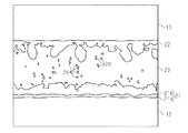
上述したように、IMCは、濡れ性が悪い上、固くて脆い特性を有する。一方、Snは、濡れ性が良い上、IMCに比べて展性、延性に富む傾向にある。この実施形態の接合構造20は、Cu配線12に接合された第1のIMC層21と、素子電極14に接合された第2のIMC層22と、第1のIMC層21と第2のIMC層22との間に中間層25とを備えている。中間層25では、Sn23中に、ネットワーク状IMC24が存在している。そのため、Snと同等の良好な濡れ性を確保できると共に、高い耐熱衝撃性を有する。また、接合作業は、Snの融点より高く、溶融したSnがCuと金属間化合物を生成する250〜350℃程度の、従来の鉛半田と同等かそれ以下の低温で行うことができる。それと共に、一旦接合した後は、415℃の高温の融点まで接合が確保される。したがって、Cu層とSn層とが積層されて配置されるため、フラックスレスで接合作業を行うことができる。また、第1のIMC層21、第2のIMC層22及び中間層25により、従来の高温鉛半田で接合された接合構造と同等の特性を有することができる。
(1)接合構造20は、Cu配線12(第1部材)と半導体素子13(第2部材)の素子電極14とを接合する接合構造である。接合構造20は、Cu配線12と素子電極14との間に存在し、Cu配線12の界面に生成された第1のIMC層21(CuとSnの金属間化合物層)と、素子電極14の界面に生成された第2のIMC層22(CuとSnの金属間化合物層)と、両金属間化合物層との間に存在しかつSn23中にネットワーク状IMC(ネットワーク状のCuとSnの金属間化合物)24が存在する中間層25とを備える。
次に、第2の実施形態を説明する。第2実施形態は、接合構造20を構成するために必要なSnを、Cu配線12の表面全体に形成したSnメッキ15として供給するのではなく、Sn箔を用いて接合する点で、第1の実施形態と大きく異なる。このSn箔は、ダイボンドを行う半導体素子13の素子電極14のサイズと合うように加工されている。図4に示すように、まず、Cu配線12上において、ダイボンドを行う所定の位置に、接合材としてのSn箔16を配置する。Sn箔16は、ダイボンドする半導体素子13のサイズに合うように加工されている。そして、Sn箔16の上に半導体素子13を載せた状態で、H2還元炉にて溶融接合が行われる。
IMCは、Snが溶融するのとほぼ同時に、Cuの界面に生成される。また、濡れ性はSnが良い一方、IMCは悪い。よって、濡れ性の良いSnが十分に濡れ広がる前に界面に発生したIMCによって、Snの濡れ広がりが阻害された結果、ボイドが発生し易くなる可能性がある。そこで、適した厚さのNi膜をCu配線12の表面に形成することで、IMCによる濡れ性の阻害を抑制することができる。
IMCのCu6Sn5は、温度により、その結晶構造を六方晶と単斜晶との間で変態することが知られている。高温では、六方晶が安定した結晶構造であり、低温では、単斜晶が安定した結晶構造である。また、両結晶構造間の変化に伴い、体積も変化する。具体的には、六方晶から単斜晶に変化する際、2.15%程度の体積増加を伴う。よって、この体積増加が、接合部分に内部応力を発生させるため、クラック発生の要因となり得る。
次に、第3の実施形態を説明する。第3実施形態は、接合構造20を構成するために必要なSnを、Cu配線12の表面全体に形成したSnメッキ15として供給するのではなく、接合材を用いて接合する点で、第2の実施形態と同じである。しかし、第3実施形態は、単層からなるSn箔16ではなく、複数層からなる接合材を用いる点で、第2実施形態と大きく異なる。
次に、第4の実施形態を説明する。第4実施形態は、配線基板11上に形成された第1部材としてのCu配線12上に、第2部材としての半導体素子13の素子電極14が接合されるのではなく、第1部材としてのCu板に対し、第2部材としての半導体素子13の素子電極14が接合構造20を介して接合されている点で、前記各実施形態と異なる。
・配線基板11上にCu配線12を形成したものに代えて、例えば、図7に示すように、DBA基板(Direct Brazed Aluminum基板)と呼ばれるセラミック基板(絶縁板)31にアルミニウム板(金属板)32をろう付した基板を用いてもよい。この場合、Cu層35とSn層36の両層を有する接合材19を使用する必要がある。また、アルミニウム板32の表面にNi層33を形成してもよい。
・上記の接合構造において、第1部材と第2部材とを接合する前に、Cuは、第1部材、第2部材、或いはそれ以外の別部材層の少なくとも何れか一つによって、第1部材と第2部材との間に配置されてもよい。
・更に、接合作業を還元炉ではなく、N2炉で行ってもよい。この場合、還元炉で行う場合よりも濡れ性はやや低下するが、十分に実用レベルの接合が可能である。
Claims (12)
- 第1部材と第2部材とを接合する接合構造であって、
前記第1部材と前記第2部材との間に、
接合前において、SnがCuに積層された状態で配置され、
CuとSnの金属間化合物を生成して、前記第1部材と前記第2部材とを接合し、
前記第1部材と前記第2部材との間に、
前記第1部材の界面に生成されたCuとSnの金属間化合物層と、
前記第2部材の界面に生成されたCuとSnの金属間化合物層と、
前記両金属間化合物層間に存在し、Sn中にネットワーク状のCuとSnの金属間化合物が存在する中間層と
を備え、
前記ネットワーク状のCuとSnの金属間化合物は、前記中間層内のSn中に、前記金属間化合物層間を繋ぐように分散して配置されていることを特徴とする接合構造。 - 接合前において、前記Cuは、前記第1部材、前記第2部材、或いはそれ以外の別部材層の少なくとも何れか一つによって配置されている請求項1に記載の接合構造。
- 前記Snと前記Cuは、直接接した状態で積層されている請求項1又は2に記載の接合構造。
- 前記Snと前記Cuは、前記Snと前記Cuとの間にNi層を配置した状態で積層されている請求項1又は2に記載の接合構造。
- 前記両金属間化合物層のうちの一方の金属間化合物層の界面は、他方の金属間化合物層の界面に比べて凹凸が大きい請求項1〜4のうちいずれか一項に記載の接合構造。
- 前記第1部材はCuからなり、前記第1部材の界面に生じるCuとSnの金属間化合物層は、Cu3Sn層及びCu6Sn5層からなる請求項1〜5のうちいずれか一項に記載の接合構造。
- 請求項1〜6のうちいずれか一項に記載の接合構造に用いる接合材であり、
Cu層と、少なくとも前記Cu層の片面全体にSn層とが存在することを特徴とする接合材。 - 前記Cu層と前記Sn層とは、クラッド材を構成している請求項7に記載の接合材。
- 前記Sn層は、前記Cu層に形成されたメッキ層からなる請求項7に記載の接合材。
- 前記Cu層及び前記Sn層は、箔からなる請求項7に記載の接合材。
- 前記Cu層はCu板からなり、前記Sn層は箔からなる請求項7に記載の接合材。
- 第1部材と第2部材とを接合する接合方法であって、
前記第1部材と前記第2部材との間に、SnをCuに積層した状態で加熱して、
前記第1部材との界面にCuとSnの第1の金属間化合物層を形成し、
前記第2部材との界面にCuとSnの第2の金属間化合物層を形成し、
前記第1の金属間化合物層と前記第2の金属間化合物層との間に、Sn中にネットワーク状のCuとSnの金属間化合物が前記第1の金属間化合物層と前記第2の金属間化合物層との間を繋ぐように分散して配置された中間層を形成することを特徴とする接合方法。
Applications Claiming Priority (3)
| Application Number | Priority Date | Filing Date | Title |
|---|---|---|---|
| JP2014169548 | 2014-08-22 | ||
| JP2014169548 | 2014-08-22 | ||
| PCT/JP2015/070119 WO2016027593A1 (ja) | 2014-08-22 | 2015-07-14 | 接合構造、接合材、及び接合方法 |
Publications (2)
| Publication Number | Publication Date |
|---|---|
| JPWO2016027593A1 JPWO2016027593A1 (ja) | 2017-05-25 |
| JP6380539B2 true JP6380539B2 (ja) | 2018-08-29 |
Family
ID=55350543
Family Applications (1)
| Application Number | Title | Priority Date | Filing Date |
|---|---|---|---|
| JP2016543867A Active JP6380539B2 (ja) | 2014-08-22 | 2015-07-14 | 接合構造、接合材、及び接合方法 |
Country Status (4)
| Country | Link |
|---|---|
| US (1) | US20170232562A1 (ja) |
| JP (1) | JP6380539B2 (ja) |
| DE (1) | DE112015003845T5 (ja) |
| WO (1) | WO2016027593A1 (ja) |
Families Citing this family (22)
| Publication number | Priority date | Publication date | Assignee | Title |
|---|---|---|---|---|
| US10541152B2 (en) | 2014-07-31 | 2020-01-21 | Skyworks Solutions, Inc. | Transient liquid phase material bonding and sealing structures and methods of forming same |
| TWI661494B (zh) | 2014-07-31 | 2019-06-01 | 美商西凱渥資訊處理科技公司 | 多層暫態液相接合 |
| JP6505004B2 (ja) * | 2015-11-30 | 2019-04-24 | 株式会社 日立パワーデバイス | 半導体装置およびその製造方法、パワーモジュール並びに車両 |
| JP6715093B2 (ja) * | 2016-06-10 | 2020-07-01 | マレリ株式会社 | ハンダ接合方法 |
| JP6042577B1 (ja) * | 2016-07-05 | 2016-12-14 | 有限会社 ナプラ | 多層プリフォームシート |
| JP6430473B2 (ja) * | 2016-07-21 | 2018-11-28 | 有限会社 ナプラ | 半導体装置 |
| JP2018012871A (ja) * | 2016-07-22 | 2018-01-25 | 大陽日酸株式会社 | 接合材、接合材の製造方法、及び接合体 |
| JP6777163B2 (ja) * | 2016-12-01 | 2020-10-28 | 株式会社村田製作所 | チップ型電子部品 |
| US10439587B2 (en) | 2016-12-02 | 2019-10-08 | Skyworks Solutions, Inc. | Methods of manufacturing electronic devices formed in a cavity |
| JP6621068B2 (ja) * | 2016-12-08 | 2019-12-18 | パナソニックIpマネジメント株式会社 | 実装構造体 |
| DE102017206932A1 (de) * | 2017-04-25 | 2018-10-25 | Siemens Aktiengesellschaft | Lotformteil zum Erzeugen einer Diffusionslötverbindung und Verfahren zum Erzeugen eines Lotformteils |
| DE102017004626A1 (de) * | 2017-05-15 | 2018-11-15 | Pfarr Stanztechnik Gmbh | Bleifreie Lötfolie zum Diffusionslöten |
| JP6885274B2 (ja) * | 2017-09-13 | 2021-06-09 | 株式会社豊田自動織機 | 接合構造 |
| US10388627B1 (en) * | 2018-07-23 | 2019-08-20 | Mikro Mesa Technology Co., Ltd. | Micro-bonding structure and method of forming the same |
| US10347602B1 (en) * | 2018-07-23 | 2019-07-09 | Mikro Mesa Technology Co., Ltd. | Micro-bonding structure |
| JP7198479B2 (ja) * | 2018-08-31 | 2023-01-04 | 学校法人早稲田大学 | 半導体素子接合構造、半導体素子接合構造の生成方法及び導電性接合剤 |
| JP7180392B2 (ja) * | 2019-01-11 | 2022-11-30 | 株式会社デンソー | 半導体装置及びその製造方法 |
| JP7310482B2 (ja) * | 2019-03-14 | 2023-07-19 | 株式会社豊田自動織機 | 接合構造及び液相拡散接合方法 |
| US11453089B2 (en) * | 2019-09-18 | 2022-09-27 | Napra Co., Ltd. | Bonding structure |
| EP4122624A4 (en) * | 2020-03-19 | 2023-08-30 | Mitsui Mining & Smelting Co., Ltd. | ASSEMBLY SHEET AND ASSEMBLED STRUCTURE |
| JP6871524B1 (ja) * | 2020-03-23 | 2021-05-12 | 千住金属工業株式会社 | 積層接合材料、半導体パッケージおよびパワーモジュール |
| DE102021119288A1 (de) | 2021-07-26 | 2023-01-26 | Infineon Technologies Ag | Elektronisches System, welches eine intermetallische Verbindungsstruktur mit einer zentralen intermetallischen Netzstruktur und netzfreie äußere Strukturen hat |
Family Cites Families (16)
| Publication number | Priority date | Publication date | Assignee | Title |
|---|---|---|---|---|
| JPH01140509A (ja) * | 1987-11-27 | 1989-06-01 | Nippon Mining Co Ltd | 通電用クラッド材 |
| JPH0360051A (ja) * | 1989-07-27 | 1991-03-15 | Fujitsu Ltd | 半導体装置とその製造方法 |
| JP3736452B2 (ja) * | 2000-12-21 | 2006-01-18 | 株式会社日立製作所 | はんだ箔 |
| US6630251B1 (en) * | 2002-09-23 | 2003-10-07 | Delphi Technologies, Inc. | Leach-resistant solder alloys for silver-based thick-film conductors |
| DE102005055280B3 (de) * | 2005-11-17 | 2007-04-12 | Infineon Technologies Ag | Verbindungselement zwischen Halbleiterchip und Schaltungsträger sowie Verfahren zur Herstellung und Verwendung des Verbindungselements |
| US7462926B2 (en) * | 2005-12-01 | 2008-12-09 | Asm Assembly Automation Ltd. | Leadframe comprising tin plating or an intermetallic layer formed therefrom |
| US20090057378A1 (en) * | 2007-08-27 | 2009-03-05 | Chi-Won Hwang | In-situ chip attachment using self-organizing solder |
| JP5535448B2 (ja) * | 2008-05-19 | 2014-07-02 | シャープ株式会社 | 半導体装置、半導体装置の実装方法、および半導体装置の実装構造 |
| JP5523680B2 (ja) * | 2008-05-29 | 2014-06-18 | 株式会社東芝 | 接合体、半導体装置および接合体の製造方法 |
| EP2351875B1 (en) * | 2009-01-20 | 2016-12-07 | Mitsubishi Shindoh Co., Ltd. | Conductive member and method for producing the same |
| US8466548B2 (en) * | 2011-05-31 | 2013-06-18 | Infineon Technologies Ag | Semiconductor device including excess solder |
| US8963321B2 (en) * | 2011-09-12 | 2015-02-24 | Infineon Technologies Ag | Semiconductor device including cladded base plate |
| WO2013099243A1 (ja) * | 2011-12-27 | 2013-07-04 | パナソニック株式会社 | 接合構造体 |
| JP5893528B2 (ja) * | 2012-07-27 | 2016-03-23 | 新日鉄住金マテリアルズ株式会社 | 無鉛はんだバンプ接合構造 |
| JP2014041980A (ja) * | 2012-08-23 | 2014-03-06 | International Business Maschines Corporation | はんだ接合部のエレクトロマイグレーション(em)耐性を向上させる界面合金層 |
| TWI538762B (zh) * | 2014-01-03 | 2016-06-21 | 樂金股份有限公司 | 銲球凸塊與封裝結構及其形成方法 |
-
2015
- 2015-07-14 US US15/503,093 patent/US20170232562A1/en not_active Abandoned
- 2015-07-14 DE DE112015003845.0T patent/DE112015003845T5/de not_active Withdrawn
- 2015-07-14 WO PCT/JP2015/070119 patent/WO2016027593A1/ja active Application Filing
- 2015-07-14 JP JP2016543867A patent/JP6380539B2/ja active Active
Also Published As
| Publication number | Publication date |
|---|---|
| WO2016027593A1 (ja) | 2016-02-25 |
| JPWO2016027593A1 (ja) | 2017-05-25 |
| US20170232562A1 (en) | 2017-08-17 |
| DE112015003845T5 (de) | 2017-05-18 |
Similar Documents
| Publication | Publication Date | Title |
|---|---|---|
| JP6380539B2 (ja) | 接合構造、接合材、及び接合方法 | |
| TWI505899B (zh) | A bonding method, a bonding structure, and a method for manufacturing the same | |
| US7964492B2 (en) | Semiconductor device and automotive AC generator | |
| US9393645B2 (en) | Junction material, manufacturing method thereof, and manufacturing method of junction structure | |
| TWI627686B (zh) | 半導體裝置及半導體裝置的製造方法 | |
| US10888958B2 (en) | Hybrid high temperature lead-free solder preform | |
| CN102074536A (zh) | 功率半导体装置及其制造方法 | |
| JP5578326B2 (ja) | リード部品及びその製造方法、並びに半導体パッケージ | |
| WO2013132942A1 (ja) | 接合方法、接合構造体およびその製造方法 | |
| JP4877046B2 (ja) | 半導体装置およびその製造方法 | |
| JP2009277777A (ja) | はんだボール搭載方法及び電子部品実装用部材 | |
| JP2013146764A (ja) | 接続材料及びそれを用いたはんだ付け製品 | |
| JP6885274B2 (ja) | 接合構造 | |
| KR102524698B1 (ko) | 접합체, 파워 모듈용 기판, 파워 모듈, 접합체의 제조 방법 및 파워 모듈용 기판의 제조 방법 | |
| JP6543890B2 (ja) | 高温はんだ合金 | |
| JP7553194B2 (ja) | 半導体装置およびその製造方法 | |
| JP7267522B1 (ja) | 接合部材および半導体装置 | |
| JP3596445B2 (ja) | 半田接合方法ならびに実装構造 | |
| JP5604995B2 (ja) | 半導体装置の製造方法 | |
| JP5807213B2 (ja) | 半導体装置、実装構造体、及び実装構造体の製造方法 | |
| JP2008091801A (ja) | 半導体装置およびその製造方法 | |
| JP6776621B2 (ja) | 半導体装置 | |
| JP2017216308A (ja) | はんだ接合体、はんだ接合体の製造方法 | |
| JP2015160224A (ja) | 接合用材料 | |
| JP2018149580A (ja) | 接合用多層シート及びその製造方法 |
Legal Events
| Date | Code | Title | Description |
|---|---|---|---|
| A521 | Request for written amendment filed |
Free format text: JAPANESE INTERMEDIATE CODE: A523 Effective date: 20170125 |
|
| A621 | Written request for application examination |
Free format text: JAPANESE INTERMEDIATE CODE: A621 Effective date: 20170125 |
|
| A131 | Notification of reasons for refusal |
Free format text: JAPANESE INTERMEDIATE CODE: A131 Effective date: 20180109 |
|
| A521 | Request for written amendment filed |
Free format text: JAPANESE INTERMEDIATE CODE: A523 Effective date: 20180309 |
|
| TRDD | Decision of grant or rejection written | ||
| A01 | Written decision to grant a patent or to grant a registration (utility model) |
Free format text: JAPANESE INTERMEDIATE CODE: A01 Effective date: 20180703 |
|
| A61 | First payment of annual fees (during grant procedure) |
Free format text: JAPANESE INTERMEDIATE CODE: A61 Effective date: 20180716 |
|
| R151 | Written notification of patent or utility model registration |
Ref document number: 6380539 Country of ref document: JP Free format text: JAPANESE INTERMEDIATE CODE: R151 |