JP6347935B2 - Semiconductor device - Google Patents
Semiconductor device Download PDFInfo
- Publication number
- JP6347935B2 JP6347935B2 JP2013215219A JP2013215219A JP6347935B2 JP 6347935 B2 JP6347935 B2 JP 6347935B2 JP 2013215219 A JP2013215219 A JP 2013215219A JP 2013215219 A JP2013215219 A JP 2013215219A JP 6347935 B2 JP6347935 B2 JP 6347935B2
- Authority
- JP
- Japan
- Prior art keywords
- layer
- oxide
- semiconductor layer
- oxide semiconductor
- electrode
- Prior art date
- Legal status (The legal status is an assumption and is not a legal conclusion. Google has not performed a legal analysis and makes no representation as to the accuracy of the status listed.)
- Active
Links
- 239000004065 semiconductor Substances 0.000 title claims description 309
- 239000013078 crystal Substances 0.000 claims description 35
- 239000010949 copper Substances 0.000 claims description 19
- RYGMFSIKBFXOCR-UHFFFAOYSA-N Copper Chemical compound [Cu] RYGMFSIKBFXOCR-UHFFFAOYSA-N 0.000 claims description 18
- 229910052802 copper Inorganic materials 0.000 claims description 18
- 229910052733 gallium Inorganic materials 0.000 claims description 18
- 239000000203 mixture Substances 0.000 claims description 11
- 229910052738 indium Inorganic materials 0.000 claims description 9
- 229910052725 zinc Inorganic materials 0.000 claims description 7
- 239000010410 layer Substances 0.000 description 715
- 239000010408 film Substances 0.000 description 413
- 239000000758 substrate Substances 0.000 description 195
- 239000007789 gas Substances 0.000 description 97
- 238000010438 heat treatment Methods 0.000 description 94
- 239000004973 liquid crystal related substance Substances 0.000 description 88
- 239000001301 oxygen Substances 0.000 description 81
- 229910052760 oxygen Inorganic materials 0.000 description 81
- 125000004429 atom Chemical group 0.000 description 78
- QVGXLLKOCUKJST-UHFFFAOYSA-N atomic oxygen Chemical group [O] QVGXLLKOCUKJST-UHFFFAOYSA-N 0.000 description 77
- 230000015572 biosynthetic process Effects 0.000 description 76
- 238000000034 method Methods 0.000 description 65
- VYPSYNLAJGMNEJ-UHFFFAOYSA-N Silicium dioxide Chemical compound O=[Si]=O VYPSYNLAJGMNEJ-UHFFFAOYSA-N 0.000 description 61
- 229910052814 silicon oxide Inorganic materials 0.000 description 57
- 239000012535 impurity Substances 0.000 description 54
- 229910052581 Si3N4 Inorganic materials 0.000 description 51
- HQVNEWCFYHHQES-UHFFFAOYSA-N silicon nitride Chemical compound N12[Si]34N5[Si]62N3[Si]51N64 HQVNEWCFYHHQES-UHFFFAOYSA-N 0.000 description 51
- XUIMIQQOPSSXEZ-UHFFFAOYSA-N Silicon Chemical compound [Si] XUIMIQQOPSSXEZ-UHFFFAOYSA-N 0.000 description 46
- 229910052710 silicon Inorganic materials 0.000 description 45
- 239000010703 silicon Substances 0.000 description 43
- 238000012360 testing method Methods 0.000 description 41
- 239000011701 zinc Substances 0.000 description 40
- 238000000151 deposition Methods 0.000 description 36
- 230000001681 protective effect Effects 0.000 description 36
- 238000012546 transfer Methods 0.000 description 35
- 230000008021 deposition Effects 0.000 description 33
- IJGRMHOSHXDMSA-UHFFFAOYSA-N Atomic nitrogen Chemical compound N#N IJGRMHOSHXDMSA-UHFFFAOYSA-N 0.000 description 29
- UFHFLCQGNIYNRP-UHFFFAOYSA-N Hydrogen Chemical compound [H][H] UFHFLCQGNIYNRP-UHFFFAOYSA-N 0.000 description 29
- 229910052739 hydrogen Inorganic materials 0.000 description 28
- 239000001257 hydrogen Substances 0.000 description 28
- XKRFYHLGVUSROY-UHFFFAOYSA-N Argon Chemical compound [Ar] XKRFYHLGVUSROY-UHFFFAOYSA-N 0.000 description 25
- 239000003990 capacitor Substances 0.000 description 25
- 238000005401 electroluminescence Methods 0.000 description 25
- 229910052751 metal Inorganic materials 0.000 description 24
- 238000004544 sputter deposition Methods 0.000 description 24
- MYMOFIZGZYHOMD-UHFFFAOYSA-N Dioxygen Chemical compound O=O MYMOFIZGZYHOMD-UHFFFAOYSA-N 0.000 description 23
- 238000004458 analytical method Methods 0.000 description 23
- 229910001882 dioxygen Inorganic materials 0.000 description 22
- 239000002184 metal Substances 0.000 description 22
- 238000010521 absorption reaction Methods 0.000 description 19
- 229910052782 aluminium Inorganic materials 0.000 description 18
- 238000004519 manufacturing process Methods 0.000 description 17
- QGZKDVFQNNGYKY-UHFFFAOYSA-N Ammonia Chemical compound N QGZKDVFQNNGYKY-UHFFFAOYSA-N 0.000 description 16
- 230000007547 defect Effects 0.000 description 16
- 238000005259 measurement Methods 0.000 description 16
- 230000006870 function Effects 0.000 description 15
- 230000000052 comparative effect Effects 0.000 description 14
- XLYOFNOQVPJJNP-UHFFFAOYSA-N water Substances O XLYOFNOQVPJJNP-UHFFFAOYSA-N 0.000 description 14
- 229910001868 water Inorganic materials 0.000 description 14
- 229910052786 argon Inorganic materials 0.000 description 13
- 239000011521 glass Substances 0.000 description 13
- WFKWXMTUELFFGS-UHFFFAOYSA-N tungsten Chemical compound [W] WFKWXMTUELFFGS-UHFFFAOYSA-N 0.000 description 13
- 229910052721 tungsten Inorganic materials 0.000 description 13
- 239000010937 tungsten Substances 0.000 description 13
- PXHVJJICTQNCMI-UHFFFAOYSA-N Nickel Chemical compound [Ni] PXHVJJICTQNCMI-UHFFFAOYSA-N 0.000 description 12
- XAGFODPZIPBFFR-UHFFFAOYSA-N aluminium Chemical compound [Al] XAGFODPZIPBFFR-UHFFFAOYSA-N 0.000 description 12
- 230000005684 electric field Effects 0.000 description 12
- 229910052757 nitrogen Inorganic materials 0.000 description 12
- 125000004430 oxygen atom Chemical group O* 0.000 description 12
- 238000005229 chemical vapour deposition Methods 0.000 description 11
- 238000001514 detection method Methods 0.000 description 11
- 239000011261 inert gas Substances 0.000 description 11
- 230000007246 mechanism Effects 0.000 description 11
- 230000001590 oxidative effect Effects 0.000 description 11
- 239000002245 particle Substances 0.000 description 11
- RTAQQCXQSZGOHL-UHFFFAOYSA-N Titanium Chemical compound [Ti] RTAQQCXQSZGOHL-UHFFFAOYSA-N 0.000 description 10
- 238000006243 chemical reaction Methods 0.000 description 10
- 229910052732 germanium Inorganic materials 0.000 description 10
- 229910052719 titanium Inorganic materials 0.000 description 10
- 239000010936 titanium Substances 0.000 description 10
- 238000012545 processing Methods 0.000 description 9
- 239000002156 adsorbate Substances 0.000 description 8
- GNPVGFCGXDBREM-UHFFFAOYSA-N germanium atom Chemical compound [Ge] GNPVGFCGXDBREM-UHFFFAOYSA-N 0.000 description 8
- 230000003287 optical effect Effects 0.000 description 8
- TWNQGVIAIRXVLR-UHFFFAOYSA-N oxo(oxoalumanyloxy)alumane Chemical compound O=[Al]O[Al]=O TWNQGVIAIRXVLR-UHFFFAOYSA-N 0.000 description 8
- 238000001004 secondary ion mass spectrometry Methods 0.000 description 8
- OKTJSMMVPCPJKN-UHFFFAOYSA-N Carbon Chemical compound [C] OKTJSMMVPCPJKN-UHFFFAOYSA-N 0.000 description 7
- VYZAMTAEIAYCRO-UHFFFAOYSA-N Chromium Chemical compound [Cr] VYZAMTAEIAYCRO-UHFFFAOYSA-N 0.000 description 7
- 238000004435 EPR spectroscopy Methods 0.000 description 7
- 238000000231 atomic layer deposition Methods 0.000 description 7
- 229910052799 carbon Inorganic materials 0.000 description 7
- 238000004040 coloring Methods 0.000 description 7
- 238000003795 desorption Methods 0.000 description 7
- 238000010586 diagram Methods 0.000 description 7
- 230000005669 field effect Effects 0.000 description 7
- 229910052735 hafnium Inorganic materials 0.000 description 7
- 150000002431 hydrogen Chemical class 0.000 description 7
- 150000002500 ions Chemical class 0.000 description 7
- 230000008569 process Effects 0.000 description 7
- 229910052726 zirconium Inorganic materials 0.000 description 7
- GYHNNYVSQQEPJS-UHFFFAOYSA-N Gallium Chemical compound [Ga] GYHNNYVSQQEPJS-UHFFFAOYSA-N 0.000 description 6
- 229910052804 chromium Inorganic materials 0.000 description 6
- 239000011651 chromium Substances 0.000 description 6
- MRELNEQAGSRDBK-UHFFFAOYSA-N lanthanum(3+);oxygen(2-) Chemical compound [O-2].[O-2].[O-2].[La+3].[La+3] MRELNEQAGSRDBK-UHFFFAOYSA-N 0.000 description 6
- PLDDOISOJJCEMH-UHFFFAOYSA-N neodymium(3+);oxygen(2-) Chemical compound [O-2].[O-2].[O-2].[Nd+3].[Nd+3] PLDDOISOJJCEMH-UHFFFAOYSA-N 0.000 description 6
- 229910052759 nickel Inorganic materials 0.000 description 6
- 238000005192 partition Methods 0.000 description 6
- -1 peroxide radicals Chemical class 0.000 description 6
- 238000004549 pulsed laser deposition Methods 0.000 description 6
- 239000002356 single layer Substances 0.000 description 6
- 229910052727 yttrium Inorganic materials 0.000 description 6
- 238000002441 X-ray diffraction Methods 0.000 description 5
- QCWXUUIWCKQGHC-UHFFFAOYSA-N Zirconium Chemical compound [Zr] QCWXUUIWCKQGHC-UHFFFAOYSA-N 0.000 description 5
- 229910002091 carbon monoxide Inorganic materials 0.000 description 5
- AJNVQOSZGJRYEI-UHFFFAOYSA-N digallium;oxygen(2-) Chemical compound [O-2].[O-2].[O-2].[Ga+3].[Ga+3] AJNVQOSZGJRYEI-UHFFFAOYSA-N 0.000 description 5
- 229910001195 gallium oxide Inorganic materials 0.000 description 5
- VBJZVLUMGGDVMO-UHFFFAOYSA-N hafnium atom Chemical compound [Hf] VBJZVLUMGGDVMO-UHFFFAOYSA-N 0.000 description 5
- SHXXPRJOPFJRHA-UHFFFAOYSA-K iron(iii) fluoride Chemical compound F[Fe](F)F SHXXPRJOPFJRHA-UHFFFAOYSA-K 0.000 description 5
- 229910052746 lanthanum Inorganic materials 0.000 description 5
- 238000001451 molecular beam epitaxy Methods 0.000 description 5
- 230000035699 permeability Effects 0.000 description 5
- 239000011347 resin Substances 0.000 description 5
- 229920005989 resin Polymers 0.000 description 5
- 125000006850 spacer group Chemical group 0.000 description 5
- 229910052684 Cerium Inorganic materials 0.000 description 4
- XEEYBQQBJWHFJM-UHFFFAOYSA-N Iron Chemical compound [Fe] XEEYBQQBJWHFJM-UHFFFAOYSA-N 0.000 description 4
- HBBGRARXTFLTSG-UHFFFAOYSA-N Lithium ion Chemical compound [Li+] HBBGRARXTFLTSG-UHFFFAOYSA-N 0.000 description 4
- 229910052779 Neodymium Inorganic materials 0.000 description 4
- GQPLMRYTRLFLPF-UHFFFAOYSA-N Nitrous Oxide Chemical compound [O-][N+]#N GQPLMRYTRLFLPF-UHFFFAOYSA-N 0.000 description 4
- BQCADISMDOOEFD-UHFFFAOYSA-N Silver Chemical compound [Ag] BQCADISMDOOEFD-UHFFFAOYSA-N 0.000 description 4
- WGLPBDUCMAPZCE-UHFFFAOYSA-N Trioxochromium Chemical compound O=[Cr](=O)=O WGLPBDUCMAPZCE-UHFFFAOYSA-N 0.000 description 4
- XLOMVQKBTHCTTD-UHFFFAOYSA-N Zinc monoxide Chemical compound [Zn]=O XLOMVQKBTHCTTD-UHFFFAOYSA-N 0.000 description 4
- 229910021417 amorphous silicon Inorganic materials 0.000 description 4
- 229910000423 chromium oxide Inorganic materials 0.000 description 4
- 229910001873 dinitrogen Inorganic materials 0.000 description 4
- 229910001416 lithium ion Inorganic materials 0.000 description 4
- 239000010453 quartz Substances 0.000 description 4
- 239000000565 sealant Substances 0.000 description 4
- 229910052709 silver Inorganic materials 0.000 description 4
- 239000004332 silver Substances 0.000 description 4
- 238000003860 storage Methods 0.000 description 4
- VWQVUPCCIRVNHF-UHFFFAOYSA-N yttrium atom Chemical compound [Y] VWQVUPCCIRVNHF-UHFFFAOYSA-N 0.000 description 4
- 239000004925 Acrylic resin Substances 0.000 description 3
- 229920000178 Acrylic resin Polymers 0.000 description 3
- ZOKXTWBITQBERF-UHFFFAOYSA-N Molybdenum Chemical compound [Mo] ZOKXTWBITQBERF-UHFFFAOYSA-N 0.000 description 3
- 229910021529 ammonia Inorganic materials 0.000 description 3
- 230000008859 change Effects 0.000 description 3
- 238000000354 decomposition reaction Methods 0.000 description 3
- 238000009826 distribution Methods 0.000 description 3
- 239000003822 epoxy resin Substances 0.000 description 3
- 239000005262 ferroelectric liquid crystals (FLCs) Substances 0.000 description 3
- YBMRDBCBODYGJE-UHFFFAOYSA-N germanium oxide Inorganic materials O=[Ge]=O YBMRDBCBODYGJE-UHFFFAOYSA-N 0.000 description 3
- 229910000449 hafnium oxide Inorganic materials 0.000 description 3
- WIHZLLGSGQNAGK-UHFFFAOYSA-N hafnium(4+);oxygen(2-) Chemical compound [O-2].[O-2].[Hf+4] WIHZLLGSGQNAGK-UHFFFAOYSA-N 0.000 description 3
- APFVFJFRJDLVQX-UHFFFAOYSA-N indium atom Chemical compound [In] APFVFJFRJDLVQX-UHFFFAOYSA-N 0.000 description 3
- 238000009434 installation Methods 0.000 description 3
- FZLIPJUXYLNCLC-UHFFFAOYSA-N lanthanum atom Chemical compound [La] FZLIPJUXYLNCLC-UHFFFAOYSA-N 0.000 description 3
- CPLXHLVBOLITMK-UHFFFAOYSA-N magnesium oxide Inorganic materials [Mg]=O CPLXHLVBOLITMK-UHFFFAOYSA-N 0.000 description 3
- 239000000395 magnesium oxide Substances 0.000 description 3
- AXZKOIWUVFPNLO-UHFFFAOYSA-N magnesium;oxygen(2-) Chemical compound [O-2].[Mg+2] AXZKOIWUVFPNLO-UHFFFAOYSA-N 0.000 description 3
- 229910052750 molybdenum Inorganic materials 0.000 description 3
- 239000011733 molybdenum Substances 0.000 description 3
- SIWVEOZUMHYXCS-UHFFFAOYSA-N oxo(oxoyttriooxy)yttrium Chemical compound O=[Y]O[Y]=O SIWVEOZUMHYXCS-UHFFFAOYSA-N 0.000 description 3
- PVADDRMAFCOOPC-UHFFFAOYSA-N oxogermanium Chemical compound [Ge]=O PVADDRMAFCOOPC-UHFFFAOYSA-N 0.000 description 3
- BPUBBGLMJRNUCC-UHFFFAOYSA-N oxygen(2-);tantalum(5+) Chemical compound [O-2].[O-2].[O-2].[O-2].[O-2].[Ta+5].[Ta+5] BPUBBGLMJRNUCC-UHFFFAOYSA-N 0.000 description 3
- RVTZCBVAJQQJTK-UHFFFAOYSA-N oxygen(2-);zirconium(4+) Chemical compound [O-2].[O-2].[Zr+4] RVTZCBVAJQQJTK-UHFFFAOYSA-N 0.000 description 3
- 238000005268 plasma chemical vapour deposition Methods 0.000 description 3
- 229910021420 polycrystalline silicon Inorganic materials 0.000 description 3
- 229920000647 polyepoxide Polymers 0.000 description 3
- 229920001721 polyimide Polymers 0.000 description 3
- 239000009719 polyimide resin Substances 0.000 description 3
- 229920002050 silicone resin Polymers 0.000 description 3
- 229910052715 tantalum Inorganic materials 0.000 description 3
- GUVRBAGPIYLISA-UHFFFAOYSA-N tantalum atom Chemical compound [Ta] GUVRBAGPIYLISA-UHFFFAOYSA-N 0.000 description 3
- 229910001936 tantalum oxide Inorganic materials 0.000 description 3
- 238000002834 transmittance Methods 0.000 description 3
- 229910001928 zirconium oxide Inorganic materials 0.000 description 3
- CURLTUGMZLYLDI-UHFFFAOYSA-N Carbon dioxide Chemical compound O=C=O CURLTUGMZLYLDI-UHFFFAOYSA-N 0.000 description 2
- 102100040844 Dual specificity protein kinase CLK2 Human genes 0.000 description 2
- 101000749291 Homo sapiens Dual specificity protein kinase CLK2 Proteins 0.000 description 2
- CBENFWSGALASAD-UHFFFAOYSA-N Ozone Chemical compound [O-][O+]=O CBENFWSGALASAD-UHFFFAOYSA-N 0.000 description 2
- KJTLSVCANCCWHF-UHFFFAOYSA-N Ruthenium Chemical compound [Ru] KJTLSVCANCCWHF-UHFFFAOYSA-N 0.000 description 2
- OUUQCZGPVNCOIJ-UHFFFAOYSA-M Superoxide Chemical compound [O-][O] OUUQCZGPVNCOIJ-UHFFFAOYSA-M 0.000 description 2
- 238000000560 X-ray reflectometry Methods 0.000 description 2
- 230000005856 abnormality Effects 0.000 description 2
- 238000009825 accumulation Methods 0.000 description 2
- 229910045601 alloy Inorganic materials 0.000 description 2
- 239000000956 alloy Substances 0.000 description 2
- 229910052787 antimony Inorganic materials 0.000 description 2
- 239000000969 carrier Substances 0.000 description 2
- ZMIGMASIKSOYAM-UHFFFAOYSA-N cerium Chemical compound [Ce][Ce][Ce][Ce][Ce][Ce][Ce][Ce][Ce][Ce][Ce][Ce][Ce][Ce][Ce][Ce][Ce][Ce][Ce][Ce][Ce][Ce][Ce][Ce][Ce][Ce][Ce][Ce][Ce][Ce][Ce][Ce][Ce][Ce][Ce][Ce][Ce][Ce] ZMIGMASIKSOYAM-UHFFFAOYSA-N 0.000 description 2
- 229910017052 cobalt Inorganic materials 0.000 description 2
- 239000010941 cobalt Substances 0.000 description 2
- GUTLYIVDDKVIGB-UHFFFAOYSA-N cobalt atom Chemical compound [Co] GUTLYIVDDKVIGB-UHFFFAOYSA-N 0.000 description 2
- 239000003086 colorant Substances 0.000 description 2
- 150000001875 compounds Chemical class 0.000 description 2
- 239000000498 cooling water Substances 0.000 description 2
- 238000005530 etching Methods 0.000 description 2
- 229910052731 fluorine Inorganic materials 0.000 description 2
- 229910003437 indium oxide Inorganic materials 0.000 description 2
- PJXISJQVUVHSOJ-UHFFFAOYSA-N indium(iii) oxide Chemical compound [O-2].[O-2].[O-2].[In+3].[In+3] PJXISJQVUVHSOJ-UHFFFAOYSA-N 0.000 description 2
- 238000002347 injection Methods 0.000 description 2
- 239000007924 injection Substances 0.000 description 2
- 150000002484 inorganic compounds Chemical class 0.000 description 2
- 229910010272 inorganic material Inorganic materials 0.000 description 2
- 229910052742 iron Inorganic materials 0.000 description 2
- 230000001788 irregular Effects 0.000 description 2
- 238000002955 isolation Methods 0.000 description 2
- 239000011777 magnesium Substances 0.000 description 2
- 238000000691 measurement method Methods 0.000 description 2
- 229910052752 metalloid Inorganic materials 0.000 description 2
- VNWKTOKETHGBQD-UHFFFAOYSA-N methane Chemical compound C VNWKTOKETHGBQD-UHFFFAOYSA-N 0.000 description 2
- 230000005012 migration Effects 0.000 description 2
- 238000013508 migration Methods 0.000 description 2
- QEFYFXOXNSNQGX-UHFFFAOYSA-N neodymium atom Chemical compound [Nd] QEFYFXOXNSNQGX-UHFFFAOYSA-N 0.000 description 2
- 239000001272 nitrous oxide Substances 0.000 description 2
- 150000002894 organic compounds Chemical class 0.000 description 2
- 230000003647 oxidation Effects 0.000 description 2
- 238000007254 oxidation reaction Methods 0.000 description 2
- 239000000047 product Substances 0.000 description 2
- 230000005855 radiation Effects 0.000 description 2
- 229910052707 ruthenium Inorganic materials 0.000 description 2
- 238000005001 rutherford backscattering spectroscopy Methods 0.000 description 2
- 238000000926 separation method Methods 0.000 description 2
- LIVNPJMFVYWSIS-UHFFFAOYSA-N silicon monoxide Chemical compound [Si-]#[O+] LIVNPJMFVYWSIS-UHFFFAOYSA-N 0.000 description 2
- 239000013589 supplement Substances 0.000 description 2
- 239000010409 thin film Substances 0.000 description 2
- XOLBLPGZBRYERU-UHFFFAOYSA-N tin dioxide Chemical compound O=[Sn]=O XOLBLPGZBRYERU-UHFFFAOYSA-N 0.000 description 2
- 229910001887 tin oxide Inorganic materials 0.000 description 2
- 238000004402 ultra-violet photoelectron spectroscopy Methods 0.000 description 2
- 229910052724 xenon Inorganic materials 0.000 description 2
- FHNFHKCVQCLJFQ-UHFFFAOYSA-N xenon atom Chemical compound [Xe] FHNFHKCVQCLJFQ-UHFFFAOYSA-N 0.000 description 2
- 239000011787 zinc oxide Substances 0.000 description 2
- MGWGWNFMUOTEHG-UHFFFAOYSA-N 4-(3,5-dimethylphenyl)-1,3-thiazol-2-amine Chemical compound CC1=CC(C)=CC(C=2N=C(N)SC=2)=C1 MGWGWNFMUOTEHG-UHFFFAOYSA-N 0.000 description 1
- UGFAIRIUMAVXCW-UHFFFAOYSA-N Carbon monoxide Chemical compound [O+]#[C-] UGFAIRIUMAVXCW-UHFFFAOYSA-N 0.000 description 1
- 102100040862 Dual specificity protein kinase CLK1 Human genes 0.000 description 1
- 101000749294 Homo sapiens Dual specificity protein kinase CLK1 Proteins 0.000 description 1
- DGAQECJNVWCQMB-PUAWFVPOSA-M Ilexoside XXIX Chemical compound C[C@@H]1CC[C@@]2(CC[C@@]3(C(=CC[C@H]4[C@]3(CC[C@@H]5[C@@]4(CC[C@@H](C5(C)C)OS(=O)(=O)[O-])C)C)[C@@H]2[C@]1(C)O)C)C(=O)O[C@H]6[C@@H]([C@H]([C@@H]([C@H](O6)CO)O)O)O.[Na+] DGAQECJNVWCQMB-PUAWFVPOSA-M 0.000 description 1
- WHXSMMKQMYFTQS-UHFFFAOYSA-N Lithium Chemical compound [Li] WHXSMMKQMYFTQS-UHFFFAOYSA-N 0.000 description 1
- FYYHWMGAXLPEAU-UHFFFAOYSA-N Magnesium Chemical compound [Mg] FYYHWMGAXLPEAU-UHFFFAOYSA-N 0.000 description 1
- 229910000861 Mg alloy Inorganic materials 0.000 description 1
- 241001591005 Siga Species 0.000 description 1
- BLRPTPMANUNPDV-UHFFFAOYSA-N Silane Chemical compound [SiH4] BLRPTPMANUNPDV-UHFFFAOYSA-N 0.000 description 1
- 229910000577 Silicon-germanium Inorganic materials 0.000 description 1
- 239000004990 Smectic liquid crystal Substances 0.000 description 1
- 239000004974 Thermotropic liquid crystal Substances 0.000 description 1
- HCHKCACWOHOZIP-UHFFFAOYSA-N Zinc Chemical compound [Zn] HCHKCACWOHOZIP-UHFFFAOYSA-N 0.000 description 1
- LEVVHYCKPQWKOP-UHFFFAOYSA-N [Si].[Ge] Chemical compound [Si].[Ge] LEVVHYCKPQWKOP-UHFFFAOYSA-N 0.000 description 1
- 230000001133 acceleration Effects 0.000 description 1
- 230000009471 action Effects 0.000 description 1
- 230000004888 barrier function Effects 0.000 description 1
- 230000008901 benefit Effects 0.000 description 1
- 230000005540 biological transmission Effects 0.000 description 1
- 229910002092 carbon dioxide Inorganic materials 0.000 description 1
- 239000001569 carbon dioxide Substances 0.000 description 1
- 239000000919 ceramic Substances 0.000 description 1
- 230000003098 cholesteric effect Effects 0.000 description 1
- 238000002485 combustion reaction Methods 0.000 description 1
- 238000004891 communication Methods 0.000 description 1
- 238000002425 crystallisation Methods 0.000 description 1
- 230000008025 crystallization Effects 0.000 description 1
- 230000006866 deterioration Effects 0.000 description 1
- 238000009792 diffusion process Methods 0.000 description 1
- PZPGRFITIJYNEJ-UHFFFAOYSA-N disilane Chemical compound [SiH3][SiH3] PZPGRFITIJYNEJ-UHFFFAOYSA-N 0.000 description 1
- 239000006185 dispersion Substances 0.000 description 1
- 238000010494 dissociation reaction Methods 0.000 description 1
- 230000005593 dissociations Effects 0.000 description 1
- 238000000295 emission spectrum Methods 0.000 description 1
- 238000011156 evaluation Methods 0.000 description 1
- 230000001747 exhibiting effect Effects 0.000 description 1
- 230000008014 freezing Effects 0.000 description 1
- 238000007710 freezing Methods 0.000 description 1
- 229910052736 halogen Inorganic materials 0.000 description 1
- 150000002367 halogens Chemical class 0.000 description 1
- 230000017525 heat dissipation Effects 0.000 description 1
- 229910052734 helium Inorganic materials 0.000 description 1
- SWQJXJOGLNCZEY-UHFFFAOYSA-N helium atom Chemical group [He] SWQJXJOGLNCZEY-UHFFFAOYSA-N 0.000 description 1
- 230000005525 hole transport Effects 0.000 description 1
- 125000004435 hydrogen atom Chemical group [H]* 0.000 description 1
- 230000006872 improvement Effects 0.000 description 1
- 238000009413 insulation Methods 0.000 description 1
- 239000012212 insulator Substances 0.000 description 1
- 238000001659 ion-beam spectroscopy Methods 0.000 description 1
- 229910052743 krypton Inorganic materials 0.000 description 1
- DNNSSWSSYDEUBZ-UHFFFAOYSA-N krypton atom Chemical group [Kr] DNNSSWSSYDEUBZ-UHFFFAOYSA-N 0.000 description 1
- 238000003475 lamination Methods 0.000 description 1
- 229910052744 lithium Inorganic materials 0.000 description 1
- 229910052749 magnesium Inorganic materials 0.000 description 1
- 238000012423 maintenance Methods 0.000 description 1
- 230000014759 maintenance of location Effects 0.000 description 1
- 239000000463 material Substances 0.000 description 1
- 239000011159 matrix material Substances 0.000 description 1
- 230000008018 melting Effects 0.000 description 1
- 238000002844 melting Methods 0.000 description 1
- QSHDDOUJBYECFT-UHFFFAOYSA-N mercury Chemical compound [Hg] QSHDDOUJBYECFT-UHFFFAOYSA-N 0.000 description 1
- 229910052753 mercury Inorganic materials 0.000 description 1
- 229910001507 metal halide Inorganic materials 0.000 description 1
- 150000005309 metal halides Chemical class 0.000 description 1
- 239000013081 microcrystal Substances 0.000 description 1
- 229910021421 monocrystalline silicon Inorganic materials 0.000 description 1
- 239000002159 nanocrystal Substances 0.000 description 1
- 229910052754 neon Inorganic materials 0.000 description 1
- GKAOGPIIYCISHV-UHFFFAOYSA-N neon atom Chemical group [Ne] GKAOGPIIYCISHV-UHFFFAOYSA-N 0.000 description 1
- JCXJVPUVTGWSNB-UHFFFAOYSA-N nitrogen dioxide Inorganic materials O=[N]=O JCXJVPUVTGWSNB-UHFFFAOYSA-N 0.000 description 1
- 230000003071 parasitic effect Effects 0.000 description 1
- 238000002161 passivation Methods 0.000 description 1
- 230000002093 peripheral effect Effects 0.000 description 1
- 238000009832 plasma treatment Methods 0.000 description 1
- 238000005498 polishing Methods 0.000 description 1
- 230000000750 progressive effect Effects 0.000 description 1
- 239000002994 raw material Substances 0.000 description 1
- 238000005057 refrigeration Methods 0.000 description 1
- 230000008929 regeneration Effects 0.000 description 1
- 238000011069 regeneration method Methods 0.000 description 1
- 238000009877 rendering Methods 0.000 description 1
- 229910052594 sapphire Inorganic materials 0.000 description 1
- 239000010980 sapphire Substances 0.000 description 1
- 229910000077 silane Inorganic materials 0.000 description 1
- 150000004756 silanes Chemical class 0.000 description 1
- HBMJWWWQQXIZIP-UHFFFAOYSA-N silicon carbide Chemical compound [Si+]#[C-] HBMJWWWQQXIZIP-UHFFFAOYSA-N 0.000 description 1
- 229910010271 silicon carbide Inorganic materials 0.000 description 1
- 239000000779 smoke Substances 0.000 description 1
- 229910052708 sodium Inorganic materials 0.000 description 1
- 239000011734 sodium Substances 0.000 description 1
- 238000001179 sorption measurement Methods 0.000 description 1
- 238000004611 spectroscopical analysis Methods 0.000 description 1
- 238000001228 spectrum Methods 0.000 description 1
- 239000011029 spinel Substances 0.000 description 1
- 229910052596 spinel Inorganic materials 0.000 description 1
- 230000000087 stabilizing effect Effects 0.000 description 1
- 238000012916 structural analysis Methods 0.000 description 1
- VEDJZFSRVVQBIL-UHFFFAOYSA-N trisilane Chemical compound [SiH3][SiH2][SiH3] VEDJZFSRVVQBIL-UHFFFAOYSA-N 0.000 description 1
- 229910052720 vanadium Inorganic materials 0.000 description 1
- GPPXJZIENCGNKB-UHFFFAOYSA-N vanadium Chemical compound [V]#[V] GPPXJZIENCGNKB-UHFFFAOYSA-N 0.000 description 1
Images


Classifications
-
- H—ELECTRICITY
- H10—SEMICONDUCTOR DEVICES; ELECTRIC SOLID-STATE DEVICES NOT OTHERWISE PROVIDED FOR
- H10B—ELECTRONIC MEMORY DEVICES
- H10B63/00—Resistance change memory devices, e.g. resistive RAM [ReRAM] devices
- H10B63/20—Resistance change memory devices, e.g. resistive RAM [ReRAM] devices comprising selection components having two electrodes, e.g. diodes
- H10B63/22—Resistance change memory devices, e.g. resistive RAM [ReRAM] devices comprising selection components having two electrodes, e.g. diodes of the metal-insulator-metal type
-
- H—ELECTRICITY
- H01—ELECTRIC ELEMENTS
- H01L—SEMICONDUCTOR DEVICES NOT COVERED BY CLASS H10
- H01L29/00—Semiconductor devices adapted for rectifying, amplifying, oscillating or switching, or capacitors or resistors with at least one potential-jump barrier or surface barrier, e.g. PN junction depletion layer or carrier concentration layer; Details of semiconductor bodies or of electrodes thereof ; Multistep manufacturing processes therefor
- H01L29/66—Types of semiconductor device ; Multistep manufacturing processes therefor
- H01L29/68—Types of semiconductor device ; Multistep manufacturing processes therefor controllable by only the electric current supplied, or only the electric potential applied, to an electrode which does not carry the current to be rectified, amplified or switched
- H01L29/76—Unipolar devices, e.g. field effect transistors
- H01L29/772—Field effect transistors
- H01L29/78—Field effect transistors with field effect produced by an insulated gate
- H01L29/786—Thin film transistors, i.e. transistors with a channel being at least partly a thin film
- H01L29/7869—Thin film transistors, i.e. transistors with a channel being at least partly a thin film having a semiconductor body comprising an oxide semiconductor material, e.g. zinc oxide, copper aluminium oxide, cadmium stannate
-
- G—PHYSICS
- G02—OPTICS
- G02F—OPTICAL DEVICES OR ARRANGEMENTS FOR THE CONTROL OF LIGHT BY MODIFICATION OF THE OPTICAL PROPERTIES OF THE MEDIA OF THE ELEMENTS INVOLVED THEREIN; NON-LINEAR OPTICS; FREQUENCY-CHANGING OF LIGHT; OPTICAL LOGIC ELEMENTS; OPTICAL ANALOGUE/DIGITAL CONVERTERS
- G02F1/00—Devices or arrangements for the control of the intensity, colour, phase, polarisation or direction of light arriving from an independent light source, e.g. switching, gating or modulating; Non-linear optics
- G02F1/01—Devices or arrangements for the control of the intensity, colour, phase, polarisation or direction of light arriving from an independent light source, e.g. switching, gating or modulating; Non-linear optics for the control of the intensity, phase, polarisation or colour
- G02F1/13—Devices or arrangements for the control of the intensity, colour, phase, polarisation or direction of light arriving from an independent light source, e.g. switching, gating or modulating; Non-linear optics for the control of the intensity, phase, polarisation or colour based on liquid crystals, e.g. single liquid crystal display cells
- G02F1/133—Constructional arrangements; Operation of liquid crystal cells; Circuit arrangements
- G02F1/136—Liquid crystal cells structurally associated with a semi-conducting layer or substrate, e.g. cells forming part of an integrated circuit
- G02F1/1362—Active matrix addressed cells
- G02F1/1368—Active matrix addressed cells in which the switching element is a three-electrode device
-
- H—ELECTRICITY
- H01—ELECTRIC ELEMENTS
- H01L—SEMICONDUCTOR DEVICES NOT COVERED BY CLASS H10
- H01L21/00—Processes or apparatus adapted for the manufacture or treatment of semiconductor or solid state devices or of parts thereof
- H01L21/70—Manufacture or treatment of devices consisting of a plurality of solid state components formed in or on a common substrate or of parts thereof; Manufacture of integrated circuit devices or of parts thereof
-
- H—ELECTRICITY
- H01—ELECTRIC ELEMENTS
- H01L—SEMICONDUCTOR DEVICES NOT COVERED BY CLASS H10
- H01L27/00—Devices consisting of a plurality of semiconductor or other solid-state components formed in or on a common substrate
- H01L27/02—Devices consisting of a plurality of semiconductor or other solid-state components formed in or on a common substrate including semiconductor components specially adapted for rectifying, oscillating, amplifying or switching and having at least one potential-jump barrier or surface barrier; including integrated passive circuit elements with at least one potential-jump barrier or surface barrier
- H01L27/12—Devices consisting of a plurality of semiconductor or other solid-state components formed in or on a common substrate including semiconductor components specially adapted for rectifying, oscillating, amplifying or switching and having at least one potential-jump barrier or surface barrier; including integrated passive circuit elements with at least one potential-jump barrier or surface barrier the substrate being other than a semiconductor body, e.g. an insulating body
- H01L27/1214—Devices consisting of a plurality of semiconductor or other solid-state components formed in or on a common substrate including semiconductor components specially adapted for rectifying, oscillating, amplifying or switching and having at least one potential-jump barrier or surface barrier; including integrated passive circuit elements with at least one potential-jump barrier or surface barrier the substrate being other than a semiconductor body, e.g. an insulating body comprising a plurality of TFTs formed on a non-semiconducting substrate, e.g. driving circuits for AMLCDs
- H01L27/1222—Devices consisting of a plurality of semiconductor or other solid-state components formed in or on a common substrate including semiconductor components specially adapted for rectifying, oscillating, amplifying or switching and having at least one potential-jump barrier or surface barrier; including integrated passive circuit elements with at least one potential-jump barrier or surface barrier the substrate being other than a semiconductor body, e.g. an insulating body comprising a plurality of TFTs formed on a non-semiconducting substrate, e.g. driving circuits for AMLCDs with a particular composition, shape or crystalline structure of the active layer
- H01L27/1225—Devices consisting of a plurality of semiconductor or other solid-state components formed in or on a common substrate including semiconductor components specially adapted for rectifying, oscillating, amplifying or switching and having at least one potential-jump barrier or surface barrier; including integrated passive circuit elements with at least one potential-jump barrier or surface barrier the substrate being other than a semiconductor body, e.g. an insulating body comprising a plurality of TFTs formed on a non-semiconducting substrate, e.g. driving circuits for AMLCDs with a particular composition, shape or crystalline structure of the active layer with semiconductor materials not belonging to the group IV of the periodic table, e.g. InGaZnO
-
- H—ELECTRICITY
- H01—ELECTRIC ELEMENTS
- H01L—SEMICONDUCTOR DEVICES NOT COVERED BY CLASS H10
- H01L27/00—Devices consisting of a plurality of semiconductor or other solid-state components formed in or on a common substrate
- H01L27/02—Devices consisting of a plurality of semiconductor or other solid-state components formed in or on a common substrate including semiconductor components specially adapted for rectifying, oscillating, amplifying or switching and having at least one potential-jump barrier or surface barrier; including integrated passive circuit elements with at least one potential-jump barrier or surface barrier
- H01L27/12—Devices consisting of a plurality of semiconductor or other solid-state components formed in or on a common substrate including semiconductor components specially adapted for rectifying, oscillating, amplifying or switching and having at least one potential-jump barrier or surface barrier; including integrated passive circuit elements with at least one potential-jump barrier or surface barrier the substrate being other than a semiconductor body, e.g. an insulating body
- H01L27/1214—Devices consisting of a plurality of semiconductor or other solid-state components formed in or on a common substrate including semiconductor components specially adapted for rectifying, oscillating, amplifying or switching and having at least one potential-jump barrier or surface barrier; including integrated passive circuit elements with at least one potential-jump barrier or surface barrier the substrate being other than a semiconductor body, e.g. an insulating body comprising a plurality of TFTs formed on a non-semiconducting substrate, e.g. driving circuits for AMLCDs
- H01L27/1248—Devices consisting of a plurality of semiconductor or other solid-state components formed in or on a common substrate including semiconductor components specially adapted for rectifying, oscillating, amplifying or switching and having at least one potential-jump barrier or surface barrier; including integrated passive circuit elements with at least one potential-jump barrier or surface barrier the substrate being other than a semiconductor body, e.g. an insulating body comprising a plurality of TFTs formed on a non-semiconducting substrate, e.g. driving circuits for AMLCDs with a particular composition or shape of the interlayer dielectric specially adapted to the circuit arrangement
-
- H—ELECTRICITY
- H01—ELECTRIC ELEMENTS
- H01L—SEMICONDUCTOR DEVICES NOT COVERED BY CLASS H10
- H01L29/00—Semiconductor devices adapted for rectifying, amplifying, oscillating or switching, or capacitors or resistors with at least one potential-jump barrier or surface barrier, e.g. PN junction depletion layer or carrier concentration layer; Details of semiconductor bodies or of electrodes thereof ; Multistep manufacturing processes therefor
- H01L29/02—Semiconductor bodies ; Multistep manufacturing processes therefor
- H01L29/12—Semiconductor bodies ; Multistep manufacturing processes therefor characterised by the materials of which they are formed
- H01L29/24—Semiconductor bodies ; Multistep manufacturing processes therefor characterised by the materials of which they are formed including, apart from doping materials or other impurities, only semiconductor materials not provided for in groups H01L29/16, H01L29/18, H01L29/20, H01L29/22
-
- H—ELECTRICITY
- H01—ELECTRIC ELEMENTS
- H01L—SEMICONDUCTOR DEVICES NOT COVERED BY CLASS H10
- H01L29/00—Semiconductor devices adapted for rectifying, amplifying, oscillating or switching, or capacitors or resistors with at least one potential-jump barrier or surface barrier, e.g. PN junction depletion layer or carrier concentration layer; Details of semiconductor bodies or of electrodes thereof ; Multistep manufacturing processes therefor
- H01L29/66—Types of semiconductor device ; Multistep manufacturing processes therefor
- H01L29/68—Types of semiconductor device ; Multistep manufacturing processes therefor controllable by only the electric current supplied, or only the electric potential applied, to an electrode which does not carry the current to be rectified, amplified or switched
- H01L29/76—Unipolar devices, e.g. field effect transistors
- H01L29/772—Field effect transistors
- H01L29/78—Field effect transistors with field effect produced by an insulated gate
- H01L29/786—Thin film transistors, i.e. transistors with a channel being at least partly a thin film
- H01L29/78645—Thin film transistors, i.e. transistors with a channel being at least partly a thin film with multiple gate
- H01L29/78648—Thin film transistors, i.e. transistors with a channel being at least partly a thin film with multiple gate arranged on opposing sides of the channel
-
- H—ELECTRICITY
- H01—ELECTRIC ELEMENTS
- H01L—SEMICONDUCTOR DEVICES NOT COVERED BY CLASS H10
- H01L29/00—Semiconductor devices adapted for rectifying, amplifying, oscillating or switching, or capacitors or resistors with at least one potential-jump barrier or surface barrier, e.g. PN junction depletion layer or carrier concentration layer; Details of semiconductor bodies or of electrodes thereof ; Multistep manufacturing processes therefor
- H01L29/66—Types of semiconductor device ; Multistep manufacturing processes therefor
- H01L29/68—Types of semiconductor device ; Multistep manufacturing processes therefor controllable by only the electric current supplied, or only the electric potential applied, to an electrode which does not carry the current to be rectified, amplified or switched
- H01L29/76—Unipolar devices, e.g. field effect transistors
- H01L29/772—Field effect transistors
- H01L29/78—Field effect transistors with field effect produced by an insulated gate
- H01L29/786—Thin film transistors, i.e. transistors with a channel being at least partly a thin film
- H01L29/7869—Thin film transistors, i.e. transistors with a channel being at least partly a thin film having a semiconductor body comprising an oxide semiconductor material, e.g. zinc oxide, copper aluminium oxide, cadmium stannate
- H01L29/78693—Thin film transistors, i.e. transistors with a channel being at least partly a thin film having a semiconductor body comprising an oxide semiconductor material, e.g. zinc oxide, copper aluminium oxide, cadmium stannate the semiconducting oxide being amorphous
-
- H—ELECTRICITY
- H10—SEMICONDUCTOR DEVICES; ELECTRIC SOLID-STATE DEVICES NOT OTHERWISE PROVIDED FOR
- H10B—ELECTRONIC MEMORY DEVICES
- H10B99/00—Subject matter not provided for in other groups of this subclass
-
- H—ELECTRICITY
- H10—SEMICONDUCTOR DEVICES; ELECTRIC SOLID-STATE DEVICES NOT OTHERWISE PROVIDED FOR
- H10K—ORGANIC ELECTRIC SOLID-STATE DEVICES
- H10K50/00—Organic light-emitting devices
Description
本発明は、半導体装置およびその作製方法に関する。 The present invention relates to a semiconductor device and a manufacturing method thereof.
なお、本明細書中において半導体装置とは、半導体特性を利用することで機能し得る装置全般をいい、電気光学装置、半導体回路および電子機器などは全て半導体装置である。 Note that in this specification, a semiconductor device refers to any device that can function by utilizing semiconductor characteristics, and an electro-optical device, a semiconductor circuit, an electronic device, and the like are all semiconductor devices.
絶縁表面を有する基板上に形成された半導体層を用いて、トランジスタを構成する技術が注目されている。当該トランジスタは集積回路や表示装置のような半導体装置に広く応用されている。トランジスタに適用可能な半導体層としてシリコン層が知られている。 A technique for forming a transistor using a semiconductor layer formed over a substrate having an insulating surface has attracted attention. The transistor is widely applied to semiconductor devices such as integrated circuits and display devices. A silicon layer is known as a semiconductor layer applicable to a transistor.
トランジスタの半導体層に用いられるシリコン層は、用途によって非晶質シリコン層と多結晶シリコン層とが使い分けられている。例えば、大型の表示装置を構成するトランジスタに適用する場合、大面積基板への成膜技術が確立されている非晶質シリコン層を用いると好適である。一方、駆動回路を一体形成した高機能の表示装置を構成するトランジスタに適用する場合、高い電界効果移動度を有するトランジスタを作製可能な多結晶シリコン層を用いると好適である。多結晶シリコン層は、非晶質シリコン層に対し高温での熱処理、またはレーザ光処理を行うことで形成する方法が知られる。 As a silicon layer used for a semiconductor layer of a transistor, an amorphous silicon layer and a polycrystalline silicon layer are selectively used depending on applications. For example, when applied to a transistor included in a large display device, it is preferable to use an amorphous silicon layer in which a technique for forming a film over a large-area substrate is established. On the other hand, when applied to a transistor included in a high-performance display device in which a driver circuit is integrally formed, it is preferable to use a polycrystalline silicon layer capable of manufacturing a transistor having high field effect mobility. A method of forming a polycrystalline silicon layer by performing heat treatment at high temperature or laser light treatment on an amorphous silicon layer is known.
さらに、近年では酸化物半導体層が注目されている。例えば、キャリア密度が1018/cm3未満であるインジウム、ガリウムおよび亜鉛を含む酸化物半導体層を用いたトランジスタが開示されている(特許文献1参照。)。 Further, in recent years, an oxide semiconductor layer has attracted attention. For example, a transistor including an oxide semiconductor layer containing indium, gallium, and zinc whose carrier density is less than 10 18 / cm 3 is disclosed (see Patent Document 1).
酸化物半導体層は、スパッタリング法を用いて成膜できるため、大型の表示装置を構成するトランジスタに適用することができる。また、酸化物半導体層を用いたトランジスタは、高い電界効果移動度を有するため、駆動回路を一体形成した高機能の表示装置を実現できる。また、非晶質シリコン層を用いたトランジスタの生産設備の一部を改良して利用することが可能であるため、設備投資を抑えられるメリットもある。 Since the oxide semiconductor layer can be formed by a sputtering method, it can be applied to a transistor included in a large display device. In addition, since a transistor including an oxide semiconductor layer has high field effect mobility, a high-functional display device in which a driver circuit is formed can be realized. In addition, since part of the transistor production facility using the amorphous silicon layer can be improved and used, there is an advantage that capital investment can be suppressed.
ところで、酸化物半導体層を用いたトランジスタは、オフ状態において極めてリーク電流(オフ電流ともいう。)が小さいことが知られている。例えば、酸化物半導体層を用いたトランジスタの低いリーク特性を応用した低消費電力のCPUなどが開示されている(特許文献2参照。)。 By the way, it is known that a transistor including an oxide semiconductor layer has extremely small leakage current (also referred to as off-state current) in an off state. For example, a low power consumption CPU using a low leakage characteristic of a transistor including an oxide semiconductor layer is disclosed (see Patent Document 2).
酸化物半導体層を用いたトランジスタの応用が広がるに連れ、信頼性の要求が多様化している。そこで、本発明の一態様は、酸化物半導体層を用いたトランジスタに安定した電気特性を付与することを課題の一とする。また、当該トランジスタを有する信頼性の高い半導体装置を提供することを課題の一とする。 As the application of transistors using an oxide semiconductor layer spreads, the requirement for reliability is diversified. Thus, an object of one embodiment of the present invention is to provide stable electrical characteristics to a transistor including an oxide semiconductor layer. Another object is to provide a highly reliable semiconductor device including the transistor.
本発明の一態様は、酸化物層および酸化物半導体層からなる多層膜と、酸化物層と接して設けられたゲート絶縁膜と、ゲート絶縁膜を介して多層膜と重ねて設けられたゲート電極と、を有し、酸化物層は、酸化物半導体層と共通の元素を含み、かつ酸化物半導体層よりもエネルギーギャップが大きく、酸化物層と酸化物半導体層との間における組成が連続的に変化する半導体装置である。なお、酸化物層と酸化物半導体層との間における組成が連続的に変化するとは、酸化物層と酸化物半導体層との間に酸化物層と酸化物半導体層の中間の組成である酸化物層または酸化物半導体層を有することをいう。 One embodiment of the present invention is a multilayer film including an oxide layer and an oxide semiconductor layer, a gate insulating film provided in contact with the oxide layer, and a gate provided so as to overlap the multilayer film with the gate insulating film interposed therebetween The oxide layer includes an element common to the oxide semiconductor layer, has an energy gap larger than that of the oxide semiconductor layer, and has a continuous composition between the oxide layer and the oxide semiconductor layer. It is a semiconductor device that changes with time. Note that the composition between the oxide layer and the oxide semiconductor layer continuously changes means that the composition between the oxide layer and the oxide semiconductor layer is an intermediate composition between the oxide layer and the oxide semiconductor layer. It means having a physical layer or an oxide semiconductor layer.
または、本発明の一態様は、酸化物層および酸化物半導体層を含む多層膜と、酸化物層と接して設けられたゲート絶縁膜と、ゲート絶縁膜を介して多層膜と重ねて設けられたゲート電極と、を有し、酸化物層は、酸化物半導体層と共通の元素を含み、かつ酸化物半導体層よりも伝導帯下端のエネルギーが真空準位に近く、酸化物層と酸化物半導体層との間における組成が連続的に変化する半導体装置である。 Alternatively, according to one embodiment of the present invention, a multilayer film including an oxide layer and an oxide semiconductor layer, a gate insulating film provided in contact with the oxide layer, and the multilayer film provided over the gate insulating film are provided. The oxide layer includes an element common to the oxide semiconductor layer, and the energy at the lower end of the conduction band is closer to the vacuum level than the oxide semiconductor layer. This is a semiconductor device in which the composition with the semiconductor layer continuously changes.
酸化物層は、ゲート絶縁膜の対向側(酸化物半導体層のバックチャネル側ともいう。)に設けられ、伝導帯下端のエネルギーが酸化物半導体層よりも0.05eV以上、0.07eV以上、0.1eV以上または0.15eV以上、かつ2eV以下、1eV以下、0.5eV以下または0.4eV以下真空準位に近い酸化物層(バリア層とも呼ぶ。)である。このとき、酸化物半導体層にはチャネルが形成され、酸化物層にはチャネルが形成されない。また、酸化物層は酸化物半導体層と共通の元素を含むため、酸化物層と酸化物半導体層との間における組成が連続的に変化する。従って、酸化物層と酸化物半導体層との間に明確な界面が存在せず、界面準位を形成しにくい。酸化物層と酸化物半導体層との間に界面準位があると、該界面をチャネルとしたしきい値電圧の異なる第2のトランジスタが形成され、トランジスタの見かけ上のしきい値電圧が変動することがある。従って、酸化物半導体層のバックチャネル側に酸化物層を設けることにより、トランジスタのしきい値電圧などの電気特性のばらつきを低減することができる。 The oxide layer is provided on the opposite side of the gate insulating film (also referred to as the back channel side of the oxide semiconductor layer), and the energy at the lower end of the conduction band is 0.05 eV or more, 0.07 eV or more than the oxide semiconductor layer, It is an oxide layer (also referred to as a barrier layer) that has a vacuum level of 0.1 eV or more or 0.15 eV or more, 2 eV or less, 1 eV or less, 0.5 eV or less, or 0.4 eV or less. At this time, a channel is formed in the oxide semiconductor layer, and no channel is formed in the oxide layer. In addition, since the oxide layer contains elements common to the oxide semiconductor layer, the composition between the oxide layer and the oxide semiconductor layer changes continuously. Therefore, there is no clear interface between the oxide layer and the oxide semiconductor layer, and interface states are difficult to form. If there is an interface state between the oxide layer and the oxide semiconductor layer, a second transistor having a different threshold voltage with the interface as a channel is formed, and the apparent threshold voltage of the transistor varies. There are things to do. Therefore, by providing the oxide layer on the back channel side of the oxide semiconductor layer, variation in electrical characteristics such as threshold voltage of the transistor can be reduced.
酸化物半導体層にチャネルが形成されるトランジスタに安定した電気特性を付与するためには、酸化物半導体層中の不純物濃度を低減し、高純度真性化することが有効である。高純度真性化とは、酸化物半導体層を真性または実質的に真性にすることをいう。なお、実質的に真性という場合、酸化物半導体層のキャリア密度は、1×10¹⁷/cm3未満、1×1015/cm3未満、または1×1013/cm3未満である。酸化物半導体層において、主成分以外(1atomic%未満)の軽元素、半金属元素、金属元素などは不純物となる。例えば、水素、窒素、炭素、シリコン、ゲルマニウム、チタンおよびハフニウムは、酸化物半導体層中で不純物となる。酸化物半導体層中の不純物濃度を低減するためには、近接するゲート絶縁膜および酸化物層中の不純物濃度も低減することが好ましい。 In order to impart stable electric characteristics to the transistor in which a channel is formed in the oxide semiconductor layer, it is effective to reduce the impurity concentration in the oxide semiconductor layer and to achieve high purity intrinsicity. High purity intrinsic refers to making an oxide semiconductor layer intrinsic or substantially intrinsic. Note that in the case of being substantially intrinsic, the carrier density of the oxide semiconductor layer is less than 1 × 10 17 / cm 3, less than 1 × 10 15 / cm 3 , or less than 1 × 10 13 / cm 3 . In the oxide semiconductor layer, light elements, metalloid elements, metal elements, and the like other than the main component (less than 1 atomic%) are impurities. For example, hydrogen, nitrogen, carbon, silicon, germanium, titanium, and hafnium are impurities in the oxide semiconductor layer. In order to reduce the impurity concentration in the oxide semiconductor layer, it is preferable to reduce the impurity concentration in the adjacent gate insulating film and the oxide layer.
例えば、酸化物半導体層中でシリコンは、不純物準位を形成する。また、該不純物準位がトラップ中心となることがある。具体的には、酸化物半導体層のシリコン濃度を1×10¹⁹atoms/cm3未満、好ましくは5×1018atoms/cm3未満、さらに好ましくは2×1018atoms/cm3未満とする。従って、酸化物半導体層のバックチャネル側にシリコンを含む絶縁膜(酸化シリコン、酸化窒化シリコン、窒化シリコン、窒化酸化シリコンなど)が設けられないことが好ましい。 For example, silicon forms impurity levels in the oxide semiconductor layer. In addition, the impurity level may become the trap center. Specifically, the silicon concentration of the oxide semiconductor layer is less than 1 × 10 19 atoms / cm 3 , preferably less than 5 × 10 18 atoms / cm 3 , and more preferably less than 2 × 10 18 atoms / cm 3 . Therefore, it is preferable that an insulating film containing silicon (such as silicon oxide, silicon oxynitride, silicon nitride, or silicon nitride oxide) be not provided on the back channel side of the oxide semiconductor layer.
また、酸化物半導体層中で水素および窒素は、ドナー準位を形成し、キャリア密度を増大させてしまう。 In addition, hydrogen and nitrogen in the oxide semiconductor layer form donor levels and increase the carrier density.
例えば、酸化物層は、アルミニウム、シリコン、ガリウム、ゲルマニウム、イットリウム、ジルコニウム、ランタン、セリウム、ネオジムまたはハフニウム(特にアルミニウムまたはガリウム)を酸化物半導体層よりも高い原子数比で含む酸化物層とすればよい。具体的には、酸化物層として、酸化物半導体層よりも前述の元素を1.5倍以上、好ましくは2倍以上、さらに好ましくは3倍以上高い原子数比で含む酸化物層を用いる。前述の元素は酸素と強く結合するため、酸素欠損が酸化物層に生じることを抑制する機能を有する。即ち、酸化物層は酸化物半導体層よりも酸素欠損が生じにくい酸化物層である。 For example, the oxide layer is an oxide layer containing aluminum, silicon, gallium, germanium, yttrium, zirconium, lanthanum, cerium, neodymium, or hafnium (especially aluminum or gallium) at a higher atomic ratio than the oxide semiconductor layer. That's fine. Specifically, as the oxide layer, an oxide layer containing the above element in an atomic ratio higher than that of the oxide semiconductor layer by 1.5 times or more, preferably 2 times or more, more preferably 3 times or more is used. The aforementioned element is strongly bonded to oxygen and thus has a function of suppressing generation of oxygen vacancies in the oxide layer. That is, the oxide layer is an oxide layer in which oxygen vacancies are less likely to occur than in the oxide semiconductor layer.
または、酸化物半導体層がIn−M−Zn酸化物であり、酸化物層もIn−M−Zn酸化物であるとき、酸化物半導体層をIn:M:Zn=x1:y1:z1[原子数比]、酸化物層をIn:M:Zn=x2:y2:z2[原子数比]とすると、y2/x2がy1/x1よりも大きくなる酸化物半導体層および酸化物層を選択する。なお、元素MはInよりも酸素との結合力が強い金属元素であり、例えばAl、Si、Ga、Ge、Y、Zr、La、Ce、NdまたはHf(特にAlまたはGa)などが挙げられる。好ましくは、y2/x2がy1/x1よりも1.5倍以上大きくなる酸化物半導体層および酸化物層を選択する。さらに好ましくは、y2/x2がy1/x1よりも2倍以上大きくなる酸化物半導体層および酸化物層を選択する。より好ましくは、y2/x2がy1/x1よりも3倍以上大きくなる酸化物半導体層および酸化物層を選択する。このとき、酸化物半導体層において、y1がx1以上であるとトランジスタに安定した電気特性を付与できるため好ましい。ただし、y1がx1の3倍以上になると、トランジスタの電界効果移動度が低下してしまうため、y1はx1の3倍未満であると好ましい。
Alternatively, when the oxide semiconductor layer is an In-M-Zn oxide and the oxide layer is also an In-M-Zn oxide, the oxide semiconductor layer is converted to In: M: Zn = x 1 : y 1 : z. 1 atomic ratio of the oxide layer In: M: Zn = x 2 : y 2:
酸化物層の厚さは、3nm以上100nm以下、好ましくは3nm以上50nm以下とする。 The thickness of the oxide layer is 3 nm to 100 nm, preferably 3 nm to 50 nm.
また、トランジスタのソース電極およびドレイン電極は、酸化物層と接して設けられる。即ち、トランジスタのソース電極−ドレイン電極間の電流(ドレイン電流ともいう。)は、酸化物層を介して酸化物半導体層を流れることになる。 In addition, the source electrode and the drain electrode of the transistor are provided in contact with the oxide layer. That is, current between the source electrode and the drain electrode of the transistor (also referred to as drain current) flows through the oxide semiconductor layer through the oxide layer.
半導体装置が大型化または微細化していくと、半導体装置の配線抵抗の影響が大きくなってくる。そのため、配線は抵抗の低い銅を含む層を有する多層膜を用いることが好ましい。ただし、前述したように、銅は酸化物半導体層中で不純物となる。本発明の一態様に係る半導体装置では、酸化物層があることで、配線に銅を含む層を有する多層膜を用いた場合でも、酸化物半導体層中の銅濃度を低くすることができる。なお、配線の一部がソース電極およびドレイン電極として機能すると、半導体装置の作製工程が簡略化できるため、好ましい。 As the semiconductor device becomes larger or finer, the influence of the wiring resistance of the semiconductor device becomes larger. Therefore, it is preferable to use a multilayer film having a layer containing copper with low resistance as the wiring. However, as described above, copper becomes an impurity in the oxide semiconductor layer. In the semiconductor device according to one embodiment of the present invention, the presence of the oxide layer makes it possible to reduce the copper concentration in the oxide semiconductor layer even when a multilayer film including a layer containing copper is used for the wiring. Note that it is preferable that part of the wiring function as a source electrode and a drain electrode because a manufacturing process of the semiconductor device can be simplified.
本発明の一態様により、酸化物層および酸化物半導体層を含む多層膜を用いることで、トランジスタに安定した電気特性を付与することができる。また、当該トランジスタを有する信頼性の高い半導体装置を提供することができる。 According to one embodiment of the present invention, stable electrical characteristics can be imparted to a transistor by using a multilayer film including an oxide layer and an oxide semiconductor layer. In addition, a highly reliable semiconductor device including the transistor can be provided.
以下では、本発明の実施の形態について図面を用いて詳細に説明する。ただし、本発明は以下の説明に限定されず、その形態および詳細を様々に変更し得ることは当業者であれば容易に理解される。また、本発明は以下に示す実施の形態の記載内容に限定して解釈されるものではない。なお、図面を用いて発明の構成を説明するにあたり、同じものを指す符号は異なる図面間でも共通して用いる。なお、同様のものを指す際にはハッチパターンを同じくし、特に符号を付さない場合がある。 Hereinafter, embodiments of the present invention will be described in detail with reference to the drawings. However, the present invention is not limited to the following description, and it will be easily understood by those skilled in the art that modes and details can be variously changed. In addition, the present invention is not construed as being limited to the description of the embodiments below. Note that in describing the structure of the present invention with reference to drawings, the same portions are denoted by the same reference numerals in different drawings. In addition, when referring to the same thing, a hatch pattern is made the same and there is a case where it does not attach a code in particular.
第1、第2として付される序数詞は便宜上用いるものであり、工程順または積層順を示すものではない。また、本明細書において発明を特定するための事項として固有の名称を示すものではない。 The ordinal numbers attached as the first and second are used for convenience, and do not indicate the order of steps or the order of lamination. In addition, a specific name is not shown as a matter for specifying the invention in this specification.
また、電圧は、ある電位と、基準の電位(例えば接地電位(GND)またはソース電位)との電位差のことを示す場合が多い。よって、電圧を電位と言い換えることが可能である。 In many cases, the voltage indicates a potential difference between a certain potential and a reference potential (for example, a ground potential (GND) or a source potential). Thus, a voltage can be rephrased as a potential.
また、「電気的に接続する」と表現される場合であっても、現実の回路においては、物理的な接続部分がなく、配線が延在しているだけの場合もある。 Even when expressed as “electrically connected”, in an actual circuit, there is a case where there is no physical connection portion and the wiring is merely extended.
また、ソースおよびドレインの機能は、回路動作において電流の方向が変化する場合などには入れ替わることがある。このため、本明細書においては、ソースおよびドレインの用語は、入れ替えて用いることができるものとする。 In addition, the functions of the source and drain may be interchanged when the direction of current changes during circuit operation. Therefore, in this specification, the terms source and drain can be used interchangeably.
なお、本実施の形態に記載の内容は、適宜組み合わせて用いることができる。 Note that the contents described in this embodiment can be combined as appropriate.
<1.トランジスタについて>
以下では、多層膜106を用いたトランジスタについて説明する。
<1. About Transistor>
Hereinafter, a transistor using the
<1−1.トランジスタ構造(1)>
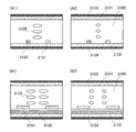
本項では、ボトムゲート型トランジスタについて説明する。ここでは、ボトムゲート型トランジスタの一種であるボトムゲートトップコンタクト構造(BGTC構造)のトランジスタについて図1を用いて説明する。
<1-1. Transistor structure (1)>
In this section, a bottom-gate transistor is described. Here, a bottom-gate top-contact (BGTC) transistor, which is a kind of bottom-gate transistor, is described with reference to FIGS.
図1に、BGTC構造であるトランジスタの上面図および断面図を示す。図1(A)は、トランジスタの上面図を示す。図1(A)において、一点鎖線A1−A2に対応する断面図を図1(B)に示す。また、図1(A)において、一点鎖線A3−A4に対応する断面図を図1(C)に示す。 FIG. 1 shows a top view and a cross-sectional view of a transistor having a BGTC structure. FIG. 1A illustrates a top view of a transistor. In FIG. 1A, a cross-sectional view corresponding to the dashed-dotted line A1-A2 is illustrated in FIG. Further, in FIG. 1A, a cross-sectional view corresponding to a dashed-dotted line A3-A4 is illustrated in FIG.
図1(B)に示すトランジスタは、基板100上に設けられたゲート電極104と、ゲート電極104上に設けられたゲート絶縁膜112と、ゲート絶縁膜112上に設けられた、酸化物半導体層106a、および酸化物半導体層106a上に設けられた酸化物層106bを含む多層膜106と、ゲート絶縁膜112および多層膜106上に設けられたソース電極116aおよびドレイン電極116bと、多層膜106、ソース電極116aおよびドレイン電極116b上に設けられた保護絶縁膜118と、を有する。
1B includes a
なお、ソース電極116aおよびドレイン電極116bに用いる導電膜の種類によっては、酸化物層106bの一部から酸素を奪い、または混合層を形成し、酸化物層106b中にソース領域106cおよびドレイン領域106dを形成することがある。
Note that depending on the type of the conductive film used for the
図1(A)において、ゲート電極104と重なる領域において、ソース電極116aとドレイン電極116bとの間隔をチャネル長という。ただし、トランジスタが、ソース領域106cおよびドレイン領域106dを含む場合、ゲート電極104と重なる領域において、ソース領域106cとドレイン領域106dとの間隔をチャネル長といってもよい。
In FIG. 1A, the distance between the
なお、チャネル形成領域とは、多層膜106において、ゲート電極104と重なり、かつソース電極116aとドレイン電極116bとに挟まれる領域をいう(図1(B)参照。)。また、チャネル領域とは、チャネル形成領域において、電流が主として流れる領域をいう。ここでは、チャネル領域は、チャネル形成領域中の酸化物半導体層106a部分である。
Note that a channel formation region refers to a region in the
なお、ゲート電極104は、図1(A)に示すように、多層膜106が内側に含まれるように設けられる。こうすることで、基板100側から光が入射した際に、多層膜106中で光によってキャリアが生成されることを抑制することができる。即ち、ゲート電極104は遮光膜としての機能を有する。ただし、ゲート電極104の外側まで多層膜106が形成されていても構わない。
Note that the
<1−1−1.多層膜について>
以下では、多層膜106、ならびに多層膜106を構成する酸化物半導体層106aおよび酸化物層106bについて説明する。
<1-1-1. About multilayer film>
Hereinafter, the
酸化物層106bは、酸化物半導体層106aを構成する酸素以外の元素一種以上から構成され、伝導帯下端のエネルギーが酸化物半導体層106aよりも0.05eV以上、0.07eV以上、0.1eV以上または0.15eV以上、かつ2eV以下、1eV以下、0.5eV以下または0.4eV以下真空準位に近い酸化物層である。このとき、ゲート電極104に電界を印加すると、多層膜106のうち、伝導帯下端のエネルギーが小さい酸化物半導体層106aにチャネルが形成される。即ち、酸化物半導体層106aと保護絶縁膜118との間に酸化物層106bを有することによって、トランジスタのチャネルを保護絶縁膜118と接しない酸化物半導体層106aに形成することができる。また、酸化物半導体層106aを構成する酸素以外の元素一種以上から酸化物層106bが構成されるため、酸化物半導体層106aと酸化物層106bとの間において、界面散乱が起こりにくい。従って、酸化物半導体層106aと酸化物層106bとの間において、キャリアの動きが阻害されないため、トランジスタの電界効果移動度が高くなる。また、酸化物半導体層106aと酸化物層106bとの間に界面準位を形成しにくい。酸化物半導体層106aと酸化物層106bとの間に界面準位があると、該界面をチャネルとしたしきい値電圧の異なる第2のトランジスタが形成され、トランジスタの見かけ上のしきい値電圧が変動することがある。従って、酸化物層106bを設けることにより、トランジスタのしきい値電圧などの電気特性のばらつきを低減することができる。
The
酸化物層106bは、例えば、アルミニウム、シリコン、ガリウム、ゲルマニウム、イットリウム、ジルコニウム、ランタン、セリウム、ネオジムまたはハフニウム(特にアルミニウムまたはガリウム)を酸化物半導体層106aよりも高い原子数比で含む酸化物層とすればよい。具体的には、酸化物層106bとして、酸化物半導体層106aよりも前述の元素を1.5倍以上、好ましくは2倍以上、さらに好ましくは3倍以上高い原子数比で含む酸化物層を用いる。前述の元素は酸素と強く結合するため、酸素欠損が酸化物層に生じることを抑制する機能を有する。即ち、酸化物層106bは酸化物半導体層106aよりも酸素欠損が生じにくい酸化物層である。
The
または、酸化物半導体層106aがIn−M−Zn酸化物であり、酸化物層106bもIn−M−Zn酸化物であるとき、酸化物半導体層106aをIn:M:Zn=x1:y1:z1[原子数比]、酸化物層106bをIn:M:Zn=x2:y2:z2[原子数比]とすると、y1/x1がy2/x2よりも大きくなる酸化物層106bおよび酸化物半導体層106aを選択する。なお、元素MはInよりも酸素との結合力が強い金属元素であり、例えばAl、Si、Ga、Ge、Y、Zr、La、Ce、NdまたはHf(特にAlまたはGa)などが挙げられる。好ましくは、y1/x1がy2/x2よりも1.5倍以上大きくなる酸化物層106bおよび酸化物半導体層106aを選択する。さらに好ましくは、y1/x1がy2/x2よりも2倍以上大きくなる酸化物層106bおよび酸化物半導体層106aを選択する。より好ましくは、y1/x1がy2/x2よりも3倍以上大きくなる酸化物層106bおよび酸化物半導体層106aを選択する。このとき、酸化物半導体層106aにおいて、y1がx1以上であるとトランジスタに安定した電気特性を付与できるため好ましい。ただし、y1がx1の3倍以上になると、トランジスタの電界効果移動度が低下してしまうため、y1はx1の3倍未満であると好ましい。
Alternatively, when the
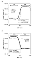
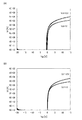
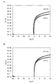
酸化物層106bは、上述の通り酸素欠損の生じにくい酸化物層である。酸化物層106bに対し、昇温脱離ガス分光法(TDS:Thermal Desorption Spectroscopy)分析を行い、質量電荷比(m/z)が32である気体分子の放出量を測定した結果を図43に示す。なお、図43では、基板温度が50℃から測定を開始し、基板温度が420℃となったところまでの結果を示す。
The
シリコンウェハ上に、酸化物層106bとして、In−Ga−Zn酸化物(In:Ga:Zn=1:3:2[原子数比])であるターゲットを用いて、スパッタリング法にて厚さが35nmとなるように成膜した。なお、酸化物層106bの成膜は、アルゴンガスおよび酸素ガスを混合した成膜ガスを用い、圧力を0.6Paとし、基板の温度を170℃とし、AC電力を5kW印加することで行った。
A thickness of the
なお、酸素割合が10%(アルゴンガス:酸素ガス=9:1)のときの酸化物層106bのTDS分析結果を図43(A)に、酸素割合が50%(アルゴンガス:酸素ガス=1:1)のときの酸化物層106bのTDS分析結果を図43(B)に、酸素割合が100%(アルゴンガス:酸素ガス=0:1)のときの酸化物層106bのTDS分析結果を図43(C)に、それぞれ示す。
Note that FIG. 43A shows the TDS analysis result of the
図43より、いずれの酸化物層106bも、50℃から420℃の範囲において、酸素分子の放出がほとんど確認されないことがわかった。従って、酸化物層106bは酸素欠損の生じにくい酸化物層であることがわかる。
From FIG. 43, it was found that almost no release of oxygen molecules was observed in any
次に、酸化物層106bの緻密さついて説明する。酸化物層106bが緻密であると、製造時のプラズマなどによってダメージが入りにくく、安定した電気特性のトランジスタとすることができる。
Next, the density of the
酸化物層106bの膜密度を、X線反射率(XRR:X−Ray Reflection)測定法によって評価した。なお、石英基板上に、測定対象である酸化物層106bを、In−Ga−Zn酸化物(In:Ga:Zn=1:3:2[原子数比])であるターゲットを用いて、スパッタリング法にて厚さが35nmとなるように成膜した。なお、酸化物層106bの成膜は、アルゴンガスおよび酸素ガスを混合した成膜ガスを用い、圧力を0.3Paまたは0.6Paとし、基板の温度を室温(約25℃)とし、AC電力を5kW印加することで行った。
The film density of the
結果、酸化物層106bの膜密度は、膜内の平均で5.75g/cm3〜5.95g/cm3と高いことがわかった。
Result, the film density of the
次に、酸化物層106bの結晶性を評価した。結晶性の評価は、X線回折(X−Ray Diffraction)によって行った。
Next, the crystallinity of the
石英基板上に、酸化物層106bとして、In−Ga−Zn酸化物(In:Ga:Zn=1:3:2[原子数比])であるターゲットを用いて、スパッタリング法にて厚さが100nmとなるように成膜した。なお、酸化物層106bの成膜は、アルゴンガスおよび酸素ガスを混合した成膜ガスを用い、圧力を0.6Paとし、AC電力を5kW印加することで行った。
A thickness of the
なお、成膜時の酸素割合は、10%(アルゴンガス:酸素ガス=9:1)、50%(アルゴンガス:酸素ガス=1:1)、100%(アルゴンガス:酸素ガス=0:1)とした。また、成膜時の基板温度は、室温(約25℃)、100℃または200℃とした。結果を図44に示す。 The oxygen ratio during film formation is 10% (argon gas: oxygen gas = 9: 1), 50% (argon gas: oxygen gas = 1: 1), 100% (argon gas: oxygen gas = 0: 1). ). The substrate temperature during film formation was room temperature (about 25 ° C.), 100 ° C. or 200 ° C. The results are shown in FIG.
図44より、酸素割合が10%で成膜した酸化物層106b、および酸素割合が50%かつ基板温度が室温で成膜した酸化物層106bは、結晶の強い配向は見られなかった。一方、上記を除く、酸素割合が50%および100%で成膜した酸化物層106bは、XRDによる鋭いピークが観測された。従って、酸素割合が50%および100%で成膜した酸化物層106bは、空間群Fd−3mに分類される結晶構造(例えば、スピネル型の結晶構造)を含んでおり、例えば、18°近傍のピークは(111)面に、36°近傍のピークは(222)面に、56°近傍のピークは(333)面に、それぞれ帰属すると考えることができる。
As shown in FIG. 44, the
酸化物層106bの厚さは、3nm以上100nm以下、好ましくは3nm以上50nm以下とする。また、酸化物半導体層106aの厚さは、3nm以上200nm以下、好ましくは3nm以上100nm以下、さらに好ましくは3nm以上50nm以下とする。
The thickness of the
以下では、酸化物半導体層106aおよび酸化物層106bのシリコン濃度について説明する。なお、トランジスタの電気特性を安定にするためには、酸化物半導体層106a中の不純物濃度を低減し、高純度真性化することが有効である。なお、酸化物半導体層106aのキャリア密度は、1×10¹⁷/cm3未満、1×1015/cm3未満、または1×1013/cm3未満とする。酸化物半導体層106aにおいて、主成分以外(1atomic%未満)の軽元素、半金属元素、金属元素などは不純物となる。例えば、水素、窒素、炭素、シリコン、ゲルマニウム、チタンおよびハフニウムは酸化物半導体層106a中で不純物となる。従って、近接するゲート絶縁膜112および酸化物層106b中の不純物濃度も低減することが好ましい。
Hereinafter, silicon concentrations of the
例えば、酸化物半導体層106aにシリコンが含まれる場合、不純物準位を形成する。特に、酸化物半導体層106aと酸化物層106bとの間にシリコンがあると、該不純物準位がトラップ中心となる。そのため、酸化物半導体層106aと酸化物層106bとの間におけるシリコン濃度を1×10¹⁹atoms/cm3未満、好ましくは5×1018atoms/cm3未満、さらに好ましくは2×1018atoms/cm3未満とする。
For example, when silicon is contained in the
また、酸化物半導体層106a中で水素および窒素は、ドナー準位を形成し、キャリア密度を増大させてしまう。酸化物半導体層106aの水素濃度は二次イオン質量分析法(SIMS:Secondary Ion Mass Spectrometry)において、2×10²⁰atoms/cm3以下、好ましくは5×1019atoms/cm3以下、より好ましくは1×1019atoms/cm3以下、さらに好ましくは5×1018atoms/cm3以下とする。また、窒素濃度は、SIMSにおいて、5×1019atoms/cm3未満、好ましくは5×1018atoms/cm3以下、より好ましくは1×1018atoms/cm3以下、さらに好ましくは5×1017atoms/cm3以下とする。
In addition, hydrogen and nitrogen in the
また、酸化物半導体層106aの水素濃度および窒素濃度を低減するために、酸化物層106bの水素濃度および窒素濃度を低減すると好ましい。酸化物層106bの水素濃度はSIMSにおいて、2×10²⁰atoms/cm3以下、好ましくは5×1019atoms/cm3以下、より好ましくは1×1019atoms/cm3以下、さらに好ましくは5×1018atoms/cm3以下とする。また、窒素濃度は、SIMSにおいて、5×1019atoms/cm3未満、好ましくは5×1018atoms/cm3以下、より好ましくは1×1018atoms/cm3以下、さらに好ましくは5×1017atoms/cm3以下とする。
In order to reduce the hydrogen concentration and the nitrogen concentration in the
なお、酸化物半導体層106aおよび酸化物層106bは、非晶質構造または結晶質構造とする。好ましくは、酸化物半導体層106aは結晶質構造とし、酸化物層106bは非晶質構造または結晶質構造とする。チャネルが形成される酸化物半導体層106aが結晶質構造であることにより、トランジスタに安定した電気特性を付与することができる。なお、結晶質構造の酸化物半導体層106aは、好ましくはCAAC−OS(C Axis Aligned Crystalline Oxide Semiconductor)層とする。
Note that the
以下では、酸化物半導体層(酸化物層)の構造について説明する。 Hereinafter, the structure of the oxide semiconductor layer (oxide layer) will be described.
なお、本明細書において、「平行」とは、二つの直線が−10°以上10°以下の角度で配置されている状態をいう。従って、−5°以上5°以下の場合も含まれる。また、「垂直」とは、二つの直線が80°以上100°以下の角度で配置されている状態をいう。したがって、85°以上95°以下の場合も含まれる。 In this specification, “parallel” refers to a state in which two straight lines are arranged at an angle of −10 ° to 10 °. Therefore, the case of −5 ° to 5 ° is also included. “Vertical” refers to a state in which two straight lines are arranged at an angle of 80 ° to 100 °. Therefore, the case of 85 ° to 95 ° is also included.
また、結晶が三方晶または菱面体晶である場合、六方晶系として表す。 Further, when the crystal is a trigonal or rhombohedral crystal, it is expressed as a hexagonal system.
酸化物半導体層は、単結晶酸化物半導体層と非単結晶酸化物半導体層とに大別される。非単結晶酸化物半導体層とは、非晶質酸化物半導体層、微結晶酸化物半導体層、多結晶酸化物半導体層、CAAC−OS層などをいう。 An oxide semiconductor layer is roughly classified into a single crystal oxide semiconductor layer and a non-single crystal oxide semiconductor layer. The non-single-crystal oxide semiconductor layer refers to an amorphous oxide semiconductor layer, a microcrystalline oxide semiconductor layer, a polycrystalline oxide semiconductor layer, a CAAC-OS layer, or the like.
非晶質酸化物半導体層は、膜中における原子配列が不規則であり、結晶成分を有さない酸化物半導体層である。微小領域においても結晶部を有さず、膜全体が完全な非晶質構造の酸化物半導体層が典型である。 The amorphous oxide semiconductor layer is an oxide semiconductor layer having an irregular atomic arrangement in the film and having no crystal component. A typical example is an oxide semiconductor layer that has no crystal part even in a minute region and has a completely amorphous structure in the entire film.
微結晶酸化物半導体層は、例えば、1nm以上10nm未満の大きさの微結晶(ナノ結晶ともいう。)を含む。したがって、微結晶酸化物半導体層は、非晶質酸化物半導体層よりも原子配列の規則性が高い。そのため、微結晶酸化物半導体層は、非晶質酸化物半導体層よりも欠陥準位密度が低いという特徴がある。 The microcrystalline oxide semiconductor layer includes a microcrystal (also referred to as nanocrystal) with a size greater than or equal to 1 nm and less than 10 nm, for example. Therefore, the microcrystalline oxide semiconductor layer has higher regularity of atomic arrangement than the amorphous oxide semiconductor layer. Therefore, the microcrystalline oxide semiconductor layer has a feature that the density of defect states is lower than that of the amorphous oxide semiconductor layer.
CAAC−OS層は、複数の結晶部を有する酸化物半導体層の一つであり、ほとんどの結晶部は、一辺が100nm未満の立方体内に収まる大きさである。したがって、CAAC−OS層に含まれる結晶部は、一辺が10nm未満、5nm未満または3nm未満の立方体内に収まる大きさの場合も含まれる。CAAC−OS層は、微結晶酸化物半導体層よりも欠陥準位密度が低いという特徴がある。以下、CAAC−OS層について詳細な説明を行う。 The CAAC-OS layer is one of oxide semiconductor layers having a plurality of crystal parts, and most of the crystal parts are large enough to fit in a cube whose one side is less than 100 nm. Therefore, the case where a crystal part included in the CAAC-OS layer fits in a cube whose one side is less than 10 nm, less than 5 nm, or less than 3 nm is included. The CAAC-OS layer is characterized by having a lower density of defect states than a microcrystalline oxide semiconductor layer. Hereinafter, the CAAC-OS layer will be described in detail.
CAAC−OS層を透過型電子顕微鏡(TEM:Transmission Electron Microscope)によって観察すると、結晶部同士の明確な境界、即ち結晶粒界(グレインバウンダリーともいう。)を確認することができない。そのため、CAAC−OS層は、結晶粒界に起因する電子移動度の低下が起こりにくいといえる。 When the CAAC-OS layer is observed with a transmission electron microscope (TEM), a clear boundary between crystal parts, that is, a crystal grain boundary (also referred to as a grain boundary) cannot be confirmed. Thus, it can be said that the CAAC-OS layer is unlikely to decrease in electron mobility due to crystal grain boundaries.
CAAC−OS層を、試料面と概略平行な方向からTEMによって観察(断面TEM観察)すると、結晶部において、金属原子が層状に配列していることを確認できる。金属原子の各層は、CAAC−OS層の膜を形成する面(被形成面ともいう。)または上面の凹凸を反映した形状であり、CAAC−OS層の被形成面または上面と平行に配列する。 When the CAAC-OS layer is observed with a TEM (cross-sectional TEM observation) from a direction substantially parallel to the sample surface, it can be confirmed that metal atoms are arranged in a layered manner in the crystal part. Each layer of metal atoms has a shape that reflects unevenness of a surface (also referred to as a formation surface) or an upper surface on which the CAAC-OS layer is formed, and is arranged in parallel with the formation surface or the upper surface of the CAAC-OS layer. .
一方、CAAC−OS層を、試料面と概略垂直な方向からTEMによって観察(平面TEM観察)すると、結晶部において、金属原子が三角形状または六角形状に配列していることを確認できる。しかしながら、異なる結晶部間で、金属原子の配列に規則性は見られない。 On the other hand, when the CAAC-OS layer is observed by TEM (planar TEM observation) from a direction substantially perpendicular to the sample surface, it can be confirmed that metal atoms are arranged in a triangular shape or a hexagonal shape in the crystal part. However, there is no regularity in the arrangement of metal atoms between different crystal parts.
断面TEM観察および平面TEM観察より、CAAC−OS層の結晶部は配向性を有していることがわかる。 From the cross-sectional TEM observation and the planar TEM observation, it is found that the crystal part of the CAAC-OS layer has orientation.
CAAC−OS層に対し、X線回折(XRD:X−Ray Diffraction)装置を用いて構造解析を行うと、例えばInGaZnO4の結晶を有するCAAC−OS層のout−of−plane法による解析では、回折角(2θ)が31°近傍にピークが現れる場合がある。このピークは、InGaZnO4の結晶の(009)面に帰属されることから、CAAC−OS層の結晶がc軸配向性を有し、c軸が被形成面または上面に概略垂直な方向を向いていることが確認できる。 When structural analysis is performed on the CAAC-OS layer using an X-ray diffraction (XRD) apparatus, for example, in the analysis of the CAAC-OS layer having an InGaZnO 4 crystal by an out-of-plane method, A peak may appear when the diffraction angle (2θ) is around 31 °. Since this peak is attributed to the (009) plane of the InGaZnO 4 crystal, the CAAC-OS layer crystal has c-axis orientation, and the c-axis is oriented in a direction substantially perpendicular to the formation surface or the top surface. Can be confirmed.
一方、CAAC−OS層に対し、c軸に概略垂直な方向からX線を入射させるin−plane法による解析では、2θが56°近傍にピークが現れる場合がある。このピークは、InGaZnO4の結晶の(110)面に帰属される。InGaZnO4の単結晶酸化物半導体層であれば、2θを56°近傍に固定し、試料面の法線ベクトルを軸(φ軸)として試料を回転させながら分析(φスキャン)を行うと、(110)面と等価な結晶面に帰属されるピークが6本観察される。これに対し、CAAC−OS層の場合は、2θを56°近傍に固定してφスキャンした場合でも、明瞭なピークが現れない。 On the other hand, in an analysis by an in-plane method in which X-rays are incident on the CAAC-OS layer from a direction substantially perpendicular to the c-axis, a peak may appear when 2θ is around 56 °. This peak is attributed to the (110) plane of the InGaZnO 4 crystal. In the case of an InGaZnO 4 single crystal oxide semiconductor layer, when 2θ is fixed at around 56 ° and analysis (φ scan) is performed while rotating the sample with the normal vector of the sample surface as the axis (φ axis), Six peaks attributed to the crystal plane equivalent to the (110) plane are observed. On the other hand, in the case of a CAAC-OS layer, a peak is not clearly observed even when φ scan is performed with 2θ fixed at around 56 °.
以上のことから、CAAC−OS層では、異なる結晶部間ではa軸およびb軸の配向は不規則であるが、c軸配向性を有し、かつc軸が被形成面または上面の法線ベクトルに平行な方向を向いていることがわかる。したがって、前述の断面TEM観察で確認された層状に配列した金属原子の各層は、結晶のab面に平行な面である。 From the above, in the CAAC-OS layer, the orientation of the a-axis and the b-axis is irregular between different crystal parts, but the c-axis is aligned, and the c-axis is a normal line of the formation surface or the top surface. It can be seen that the direction is parallel to the vector. Therefore, each layer of metal atoms arranged in a layer shape confirmed by the above-mentioned cross-sectional TEM observation is a plane parallel to the ab plane of the crystal.
なお、結晶部は、CAAC−OS層を成膜した際、または加熱処理などの結晶化処理を行った際に形成される。上述したように、結晶のc軸は、CAAC−OS層の被形成面または上面の法線ベクトルに平行な方向に配向する。したがって、例えば、CAAC−OS層の形状をエッチングなどによって変化させた場合、結晶のc軸がCAAC−OS層の被形成面または上面の法線ベクトルと平行にならないこともある。 Note that the crystal part is formed when the CAAC-OS layer is formed or when crystallization treatment such as heat treatment is performed. As described above, the c-axis of the crystal is oriented in a direction parallel to the normal vector of the formation surface or the top surface of the CAAC-OS layer. Therefore, for example, when the shape of the CAAC-OS layer is changed by etching or the like, the c-axis of the crystal may not be parallel to the normal vector of the formation surface or the top surface of the CAAC-OS layer.
また、CAAC−OS層中の結晶化度が均一でなくてもよい。例えば、CAAC−OS層の結晶部が、CAAC−OS層の上面近傍からの結晶成長によって形成される場合、上面近傍の領域は、被形成面近傍の領域よりも結晶化度が高くなることがある。また、CAAC−OS層に不純物を添加する場合、不純物が添加された領域の結晶化度が変化し、部分的に結晶化度の異なる領域が形成されることもある。 Further, the degree of crystallinity in the CAAC-OS layer is not necessarily uniform. For example, in the case where the crystal part of the CAAC-OS layer is formed by crystal growth from the vicinity of the top surface of the CAAC-OS layer, the region near the top surface can have a higher degree of crystallinity than the region near the formation surface. is there. In addition, in the case where an impurity is added to the CAAC-OS layer, the crystallinity of a region to which the impurity is added changes, and a region with a partially different crystallinity may be formed.
CAAC−OS層を用いたトランジスタは、可視光や紫外光の照射による電気特性の変動が小さい。よって、当該トランジスタは、信頼性が高い。 In a transistor using a CAAC-OS layer, change in electrical characteristics due to irradiation with visible light or ultraviolet light is small. Therefore, the transistor has high reliability.
なお、酸化物半導体層は、例えば、非晶質酸化物半導体層、微結晶酸化物半導体層、CAAC−OS層のうち、二種以上を有する積層膜であってもよい。 Note that the oxide semiconductor layer may be a stacked film including two or more of an amorphous oxide semiconductor layer, a microcrystalline oxide semiconductor layer, and a CAAC-OS layer, for example.
なお、酸化物半導体層106aにシリコンおよび炭素が高い濃度で含まれることにより、酸化物半導体層106aの結晶性を低下させることがある。酸化物半導体層106aの結晶性を低下させないためには、酸化物半導体層106aのシリコン濃度を1×10¹⁹atoms/cm3未満、好ましくは5×1018atoms/cm3未満、さらに好ましくは2×1018atoms/cm3未満とすればよい。また、酸化物半導体層106aの結晶性を低下させないためには、酸化物半導体層106aの炭素濃度を1×1019atoms/cm3未満、好ましくは5×1018atoms/cm3未満、さらに好ましくは2×1018atoms/cm3未満とすればよい。
Note that when the
このように、チャネルが形成される酸化物半導体層106aが高い結晶性を有し、かつ不純物や欠陥などに起因する準位密度が低い場合、多層膜106を用いたトランジスタは安定した電気特性を有する。
In this manner, when the
以下では、多層膜106中の局在準位について説明する。多層膜106中の局在準位密度を低減することで、多層膜106を用いたトランジスタに安定した電気特性を付与することができる。多層膜106の局在準位は、一定光電流測定法(CPM:Constant Photocurrent Method)によって評価可能である。
Hereinafter, the localized levels in the
なお、トランジスタに安定した電気特性を付与するためには、多層膜106中のCPM測定で得られる局在準位による吸収係数を、1×10⁻³cm−1未満、好ましくは3×10⁻⁴cm−1未満とすればよい。また、多層膜106中のCPM測定で得られる局在準位による吸収係数を、1×10⁻³cm−1未満、好ましくは3×10⁻⁴cm−1未満とすることで、トランジスタの電界効果移動度を高めることができる。なお、多層膜106中のCPM測定で得られる局在準位による吸収係数を、1×10⁻³cm−1未満、好ましくは3×10⁻⁴cm−1未満とするためには、酸化物半導体層106a中で局在準位を形成する元素であるシリコン、ゲルマニウム、炭素、ハフニウム、チタンなどの濃度を2×10¹⁸atoms/cm3未満、好ましくは2×1017atoms/cm3未満とすればよい。
In order to have stable electrical characteristics for the transistor, the absorption coefficient due to localized levels measured by CPM of the
CPM測定では、試料である多層膜106に接して設けられた電極および電極間に電圧を印加した状態で光電流値が一定となるように端子間の試料面に照射する光量を調整し、照射光量から吸収係数を導出することを各波長にて行うものである。CPM測定において、試料に欠陥があるとき、欠陥の存在する準位に応じたエネルギー(波長より換算)における吸収係数が増加する。この吸収係数の増加分に定数を掛けることにより、試料の欠陥密度を導出することができる。
In the CPM measurement, the amount of light applied to the sample surface between the terminals is adjusted so that the photocurrent value is constant in a state where a voltage is applied between the electrodes provided in contact with the
CPM測定で観測される局在準位は、不純物や欠陥に起因する準位と考えられる。即ち、CPM測定で観測される局在準位による吸収係数が小さい多層膜106を用いたトランジスタは安定した電気特性を有することがわかる。
Localized levels observed by CPM measurement are considered to be levels caused by impurities and defects. That is, it can be seen that the transistor using the
次に、加熱処理によって多層膜106中の酸素が、450℃の加熱処理後に拡散する様子について図2を用いて説明する。
Next, how oxygen in the
図2に、多層膜106のうち、いずれかの層を18O2ガスを用いて成膜した試料について、SIMSを行い、深さ方向における18Oの濃度分布を測定した結果を示す。
FIG. 2 shows the result of performing SIMS and measuring the concentration distribution of 18 O in the depth direction for a sample in which any one of the
ここで、酸化物半導体層106aは、In−Ga−Zn酸化物(In:Ga:Zn=3:1:2[原子数比])であるターゲットを用いて、スパッタリング法にて成膜した酸化物半導体層である。
Here, the
また、酸化物層106bは、In−Ga−Zn酸化物(In:Ga:Zn=1:1:1[原子数比])であるターゲットを用いて、スパッタリング法にて成膜した酸化物層である。
The
ここで、図2(A)は、酸化物層106bに18O2ガスを用い、酸化物半導体層106aには18O2ガスを用いていない試料の酸化物層106bおよび酸化物半導体層106aの間を含む深さ方向における18Oの濃度分布である。加熱処理なし(as−depoと表記、細実線)と比べ、450℃加熱処理後(450℃加熱後と表記、太実線)では、18Oが酸化物層106bから酸化物半導体層106aまで拡散していることがわかった。
Here, FIG. 2 (A), with 18 O 2 gas to the
また、図2(B)は、酸化物半導体層106aに18O2ガスを用い、酸化物層106bには18O2ガスを用いていない試料の酸化物半導体層106aおよび酸化物層106bの間を含む深さ方向における18Oの濃度分布である。加熱処理なし(as−depoと表記、細実線)と比べ、450℃加熱処理後(450℃加熱後と表記、太実線)では、18Oが酸化物半導体層106aから酸化物層106bまで拡散していることがわかった。
Also, FIG. 2 (B), between the oxide with 18 O 2 gas to the
図2に示すように、多層膜106中で酸素は相互に移動することがわかった。即ち、酸化物半導体層106aと酸化物層106bとの間には、酸化物半導体層106aおよび酸化物層106bの混合層が形成されていることがわかる。
As shown in FIG. 2, it was found that oxygen moves in the
以下では、多層膜106のバンド構造について、図3を用いて説明する。
Hereinafter, the band structure of the
なお、酸化物半導体層106aとしてエネルギーギャップが3.15eVであるIn−Ga−Zn酸化物を用い、酸化物層106bとしてエネルギーギャップが3.5eVであるIn−Ga−Zn酸化物とする。エネルギーギャップは、分光エリプソメータ(HORIBA JOBIN YVON社 UT−300)を用いて測定した。
Note that an In—Ga—Zn oxide with an energy gap of 3.15 eV is used as the
酸化物半導体層106aおよび酸化物層106bの真空準位と価電子帯上端のエネルギー差(イオン化ポテンシャルともいう。)は、それぞれ8eVおよび8.2eVであった。なお、真空準位と価電子帯上端のエネルギー差は、紫外線光電子分光分析(UPS:Ultraviolet Photoelectron Spectroscopy)装置(PHI社 VersaProbe)を用いて測定した。
The energy difference (also referred to as ionization potential) between the vacuum level and the top of the valence band of the
従って、酸化物半導体層106aおよび酸化物層106bの真空準位と伝導帯下端のエネルギー差(電子親和力ともいう。)は、それぞれ4.85eVおよび4.7eVであった。
Therefore, the energy difference (also referred to as electron affinity) between the vacuum level and the bottom of the conduction band of the
図3に、多層膜のバンド構造の一部を模式的に示す。図3では、酸化物半導体層106aおよび酸化物層106bのそれぞれと接する酸化シリコン層を設けた場合について説明する。ここで、EcI1は酸化シリコン層の伝導帯下端のエネルギーを示し、EcS1は酸化物半導体層106aの伝導帯下端のエネルギーを示し、EcS2は酸化物層106bの伝導帯下端のエネルギーを示し、EcI2は酸化シリコン層の伝導帯下端のエネルギーを示す。
FIG. 3 schematically shows a part of the band structure of the multilayer film. FIG. 3 illustrates the case where a silicon oxide layer in contact with each of the
図3に示すように、酸化物半導体層106aおよび酸化物層106bにおいて、伝導帯下端のエネルギーが連続的に変化する。これは、酸化物半導体層106aおよび酸化物層106b間で、酸素が相互に移動することで混合層を形成するという図2に示す結果からも理解される。
As shown in FIG. 3, in the
図3より、多層膜106の酸化物半導体層106aがウェル(井戸)となり、多層膜106を用いたトランジスタにおいて、チャネルが酸化物半導体層106aに形成されることがわかる。なお、多層膜106は伝導帯下端のエネルギーが連続的に変化しているため、酸化物半導体層106aと酸化物層106bとが連続接合している、ともいえる。
FIG. 3 shows that the
なお、図4に示すように、酸化物層106bと、保護絶縁膜118との界面近傍には、不純物や欠陥に起因したトラップ中心が形成され得るものの、酸化物層106bがあることにより、酸化物半導体層106aと当該トラップ中心とを遠ざけることができる。ただし、EcS1とEcS2とのエネルギー差が小さい場合、酸化物半導体層106aの電子が該エネルギー差を越えてトラップ中心に達することがある。トラップ中心に電子が捕獲されることで、絶縁膜界面にマイナスの固定電荷が生じ、トランジスタのしきい値電圧はプラス方向にシフトしてしまう。
Note that as shown in FIG. 4, although a trap center due to an impurity or a defect can be formed in the vicinity of the interface between the
従って、EcS1とEcS2とのエネルギー差を、それぞれ0.1eV以上、好ましくは0.15eV以上とすると、トランジスタのしきい値電圧の変動が低減され、安定した電気特性となるため、好ましい。 Therefore, it is preferable that the energy difference between EcS1 and EcS2 is 0.1 eV or more, preferably 0.15 eV or more, because fluctuations in the threshold voltage of the transistor are reduced and stable electric characteristics are obtained.
<1−1−2.ソース電極およびドレイン電極>
ソース電極116aおよびドレイン電極116bは、アルミニウム、チタン、クロム、コバルト、ニッケル、銅、イットリウム、ジルコニウム、モリブデン、ルテニウム、銀、タンタルおよびタングステンを一種以上含む導電膜を、単層で、または積層で用いればよい。好ましくは、ソース電極116aおよびドレイン電極116bは、銅を含む層を有する多層膜とする。ソース電極116aおよびドレイン電極116bを銅を含む層を有する多層膜とすることで、ソース電極116aおよびドレイン電極116bと同一層で配線を形成する場合、配線抵抗を低くすることができる。なお、ソース電極116aとドレイン電極116bは同一組成であってもよいし、異なる組成であってもよい。
<1-1-2. Source electrode and drain electrode>
The
ところで、ソース電極116aおよびドレイン電極116bとして、銅を含む層を有する多層膜を用いる場合、銅の影響により、酸化物層106bと保護絶縁膜118との界面に図4に示したようなトラップ中心を形成することがある。この場合も、酸化物層106bを有することにより、当該トラップ中心に電子が捕獲されることを抑制することができる。従って、トランジスタに安定した電気特性を付与し、かつ配線抵抗を低くすることが可能となる。
When a multilayer film having a layer containing copper is used as the
<1−1−3.保護絶縁膜>
保護絶縁膜118は、酸化アルミニウム、酸化マグネシウム、酸化シリコン、酸化窒化シリコン、窒化酸化シリコン、窒化シリコン、酸化ガリウム、酸化ゲルマニウム、酸化イットリウム、酸化ジルコニウム、酸化ランタン、酸化ネオジム、酸化ハフニウムおよび酸化タンタルを一種以上含む絶縁膜を、単層で、または積層で用いればよい。
<1-1-3. Protective insulating film>
The protective
保護絶縁膜118は、例えば、1層目を酸化シリコン層とし、2層目を窒化シリコン層とした多層膜とすればよい。この場合、酸化シリコン層は酸化窒化シリコン層でも構わない。また、窒化シリコン層は窒化酸化シリコン層でも構わない。酸化シリコン層は、欠陥密度の小さい酸化シリコン層を用いると好ましい。具体的には、電子スピン共鳴(ESR:Electron Spin Resonance)にてg値が2.001の信号に由来するスピンの密度が3×10¹⁷spins/cm3以下、好ましくは5×1016spins/cm3以下である酸化シリコン層を用いる。窒化シリコン層は水素ガスおよびアンモニアガスの放出量が少ない窒化シリコン層を用いる。水素ガス、アンモニアガスの放出量は、TDS分析にて測定すればよい。また、窒化シリコン層は、水素、水および酸素を透過しない、またはほとんど透過しない窒化シリコン層を用いる。
For example, the protective
または、保護絶縁膜118は、例えば、1層目を第1の酸化シリコン層118aとし、2層目を第2の酸化シリコン層118bとし、3層目を窒化シリコン層118cとした多層膜とすればよい(図1(D)参照。)。この場合、第1の酸化シリコン層118aまたは/および第2の酸化シリコン層118bは酸化窒化シリコン層でも構わない。また、窒化シリコン層は窒化酸化シリコン層でも構わない。第1の酸化シリコン層118aは、欠陥密度の小さい酸化シリコン層を用いると好ましい。具体的には、ESRにてg値が2.001の信号に由来するスピンの密度が3×1017spins/cm3以下、好ましくは5×1016spins/cm3以下である酸化シリコン層を用いる。第2の酸化シリコン層118bは、過剰酸素を含む酸化シリコン層を用いる。窒化シリコン層118cは水素ガスおよびアンモニアガスの放出量が少ない窒化シリコン層を用いる。また、窒化シリコン層は、水素、水および酸素を透過しない、またはほとんど透過しない窒化シリコン層を用いる。
Alternatively, the protective
過剰酸素を含む酸化シリコン層とは、加熱処理などによって酸素を放出することができる酸化シリコン層をいう。また、過剰酸素を含む絶縁膜は、加熱処理によって酸素を放出する機能を有する絶縁膜である。 A silicon oxide layer containing excess oxygen refers to a silicon oxide layer from which oxygen can be released by heat treatment or the like. The insulating film containing excess oxygen is an insulating film having a function of releasing oxygen by heat treatment.
過剰酸素を含む絶縁膜は、酸化物半導体層106a中の酸素欠損を低減することができる。酸化物半導体層106a中で酸素欠損は、欠陥準位を形成し、その一部がドナー準位となる。従って、酸化物半導体層106a中の酸素欠損を低減することで、トランジスタに安定した電気特性を付与することができる。
The insulating film containing excess oxygen can reduce oxygen vacancies in the
ここで、加熱処理によって酸素を放出する膜は、TDS分析によって1×10¹⁸atoms/cm3以上、1×1019atoms/cm3以上または1×1020atoms/cm3以上の酸素(酸素原子数に換算)を放出することもある。 Here, a film from which oxygen is released by heat treatment is an oxygen (oxygen atom) of 1 × 10 18 atoms / cm 3 or more, 1 × 10 19 atoms / cm 3 or more, or 1 × 10 20 atoms / cm 3 or more by TDS analysis. (Converted to a number).
ここで、TDS分析を用いた酸素の放出量の測定方法について、以下に説明する。 Here, a method of measuring the amount of released oxygen using TDS analysis will be described below.
測定試料をTDS分析したときの気体の全放出量は、放出ガスのイオン強度の積分値に比例する。そして標準試料との比較により、気体の全放出量を計算することができる。 The total amount of gas released when the measurement sample is subjected to TDS analysis is proportional to the integrated value of the ionic strength of the released gas. The total amount of gas released can be calculated by comparison with a standard sample.
例えば、標準試料である所定の密度の水素を含むシリコンウェハのTDS分析結果、および測定試料のTDS分析結果から、測定試料の酸素分子の放出量(NO2)は、数式(1)で求めることができる。ここで、TDS分析で得られる質量数32で検出されるガスの全てが酸素分子由来と仮定する。質量数32のものとしてほかにCH3OHがあるが、存在する可能性が低いものとしてここでは考慮しない。また、酸素原子の同位体である質量数17の酸素原子および質量数18の酸素原子を含む酸素分子についても、自然界における存在比率が極微量であるため考慮しない。 For example, from the TDS analysis result of a silicon wafer containing hydrogen of a predetermined density as a standard sample and the TDS analysis result of the measurement sample, the amount of released oxygen molecules (N O2 ) of the measurement sample is obtained by Equation (1). Can do. Here, it is assumed that all the gases detected by the mass number 32 obtained by the TDS analysis are derived from oxygen molecules. There is CH 3 OH in addition to those having a mass number of 32, but these are not considered here because they are unlikely to exist. In addition, oxygen molecules containing oxygen atoms with a mass number of 17 and oxygen atoms with a mass number of 18 which are isotopes of oxygen atoms are not considered because the existence ratio in nature is extremely small.

NH2は、標準試料から脱離した水素分子を密度で換算した値である。SH2は、標準試料をTDS分析したときのイオン強度の積分値である。ここで、標準試料の基準値を、NH2/SH2とする。SO2は、測定試料をTDS分析したときのイオン強度の積分値である。αは、TDS分析におけるイオン強度に影響する係数である。数式(1)の詳細に関しては、特開平6−275697公報を参照する。なお、上記酸素の放出量は、電子科学株式会社製の昇温脱離分析装置EMD−WA1000S/Wを用い、標準試料として1×1016atoms/cm2の水素原子を含むシリコンウェハを用いて測定した。 N H2 is a value obtained by converting hydrogen molecules desorbed from the standard sample by density. SH2 is an integral value of ion intensity when the standard sample is subjected to TDS analysis. Here, the reference value of the standard sample is N H2 / SH 2 . S O2 is an integrated value of ion intensity when the measurement sample is subjected to TDS analysis. α is a coefficient that affects the ionic strength in the TDS analysis. For details of Equation (1), refer to Japanese Patent Laid-Open No. Hei 6-275697. The oxygen release amount is determined by using a temperature-programmed desorption analyzer EMD-WA1000S / W manufactured by Electronic Science Co., Ltd., and using a silicon wafer containing 1 × 10 16 atoms / cm 2 of hydrogen atoms as a standard sample. It was measured.
また、TDS分析において、酸素の一部は酸素原子として検出される。酸素分子と酸素原子の比率は、酸素分子のイオン化率から算出することができる。なお、上述のαは酸素分子のイオン化率を含むため、酸素分子の放出量を評価することで、酸素原子の放出量についても見積もることができる。 In TDS analysis, part of oxygen is detected as oxygen atoms. The ratio of oxygen molecules to oxygen atoms can be calculated from the ionization rate of oxygen molecules. Note that since the above α includes the ionization rate of oxygen molecules, the amount of released oxygen atoms can be estimated by evaluating the amount of released oxygen molecules.
なお、NO2は酸素分子の放出量である。酸素原子に換算したときの放出量は、酸素分子の放出量の2倍となる。 Note that N 2 O 2 is the amount of released oxygen molecules. The amount of release when converted to oxygen atoms is twice the amount of release of oxygen molecules.
または、加熱処理によって酸素を放出する膜は、過酸化ラジカルを含むこともある。具体的には、過酸化ラジカルに起因するスピン密度が、5×10¹⁷spins/cm3以上であることをいう。なお、過酸化ラジカルを含む膜は、ESRにて、g値が2.01近傍に非対称の信号を有することもある。 Alternatively, the film from which oxygen is released by heat treatment may contain peroxide radicals. Specifically, it means that the spin density resulting from the peroxide radical is 5 × 10 17 spins / cm 3 or more. Note that a film containing a peroxide radical may have an asymmetric signal in the vicinity of a g value of 2.01 by ESR.
または、過剰酸素を含む絶縁膜は、酸素が過剰な酸化シリコン(SiOX(X>2))であってもよい。酸素が過剰な酸化シリコン(SiOX(X>2))は、シリコン原子数の2倍より多い酸素原子を単位体積当たりに含むものである。単位体積当たりのシリコン原子数および酸素原子数は、ラザフォード後方散乱法(RBS:Rutherford Backscattering Spectrometry)により測定した値である。 Alternatively, the insulating film containing excess oxygen may be oxygen-excess silicon oxide (SiO X (X> 2)). Oxygen-excess silicon oxide (SiO X (X> 2)) contains oxygen atoms more than twice the number of silicon atoms per unit volume. The number of silicon atoms and the number of oxygen atoms per unit volume are values measured by Rutherford Backscattering Spectroscopy (RBS: Rutherford Backscattering Spectrometry).
<1−1−4.ゲート絶縁膜>
ゲート絶縁膜112は、酸化アルミニウム、酸化マグネシウム、酸化シリコン、酸化窒化シリコン、窒化酸化シリコン、窒化シリコン、酸化ガリウム、酸化ゲルマニウム、酸化イットリウム、酸化ジルコニウム、酸化ランタン、酸化ネオジム、酸化ハフニウムおよび酸化タンタルを一種以上含む絶縁膜を、単層で、または積層で用いればよい。
<1-1-4. Gate insulation film>
The
ゲート絶縁膜112は、例えば、1層目を窒化シリコン層とし、2層目を酸化シリコン層とした多層膜とすればよい。この場合、酸化シリコン層は酸化窒化シリコン層でも構わない。また、窒化シリコン層は窒化酸化シリコン層でも構わない。酸化シリコン層は、欠陥密度の小さい酸化シリコン層を用いると好ましい。具体的にはESRにてg値が2.001の信号に由来するスピンの密度が3×10¹⁷spins/cm3以下、好ましくは5×1016spins/cm3以下である酸化シリコン層を用いる。酸化シリコン層は、過剰酸素を含む酸化シリコン層を用いると好ましい。窒化シリコン層は水素ガスおよびアンモニアガスの放出量が少ない窒化シリコン層を用いる。水素ガス、アンモニアガスの放出量は、TDS分析にて測定すればよい。
For example, the
ゲート絶縁膜112および保護絶縁膜118の少なくとも一方が過剰酸素を含む絶縁膜を含む場合、酸化物半導体層106aの酸素欠損が低減され、トランジスタに安定した電気特性を付与することができる。
In the case where at least one of the
<1−1−5.ゲート電極>
ゲート電極104は、アルミニウム、チタン、クロム、コバルト、ニッケル、銅、イットリウム、ジルコニウム、モリブデン、ルテニウム、銀、タンタルおよびタングステンを一種以上含む導電膜を、単層で、または積層で用いればよい。
<1-1-5. Gate electrode>
The
<1−1−6.基板>
基板100に大きな制限はない。例えば、ガラス基板、セラミック基板、石英基板、サファイア基板などを、基板100として用いてもよい。また、シリコンや炭化シリコンなどの単結晶半導体基板、多結晶半導体基板、シリコンゲルマニウムなどの化合物半導体基板、SOI(Silicon On Insulator)基板などを適用することも可能であり、これらの基板上に半導体素子が設けられたものを、基板100として用いてもよい。
<1-1-6. Substrate>
There is no major limitation on the
また、基板100として、第5世代(1000mm×1200mmまたは1300mm×1500mm)、第6世代(1500mm×1800mm)、第7世代(1870mm×2200mm)、第8世代(2200mm×2500mm)、第9世代(2400mm×2800mm)、第10世代(2880mm×3130mm)などの大型ガラス基板を用いる場合、半導体装置の作製工程における加熱処理などで生じる基板100の縮みによって、微細な加工が困難になる場合ある。そのため、前述したような大型ガラス基板を基板100として用いる場合、加熱処理による縮みの小さいものを用いることが好ましい。例えば、基板100として、400℃、好ましくは450℃、さらに好ましくは500℃の温度で1時間加熱処理を行った後の縮み量が10ppm以下、好ましくは5ppm以下、さらに好ましくは3ppm以下である大型ガラス基板を用いればよい。
Further, as the
また、基板100として、可とう性基板を用いてもよい。なお、可とう性基板上にトランジスタを設ける方法としては、非可とう性の基板上にトランジスタを作製した後、トランジスタを剥離し、可とう性基板である基板100に転置する方法もある。その場合には、非可とう性基板とトランジスタとの間に剥離層を設けるとよい。
Further, a flexible substrate may be used as the
以上のようにして構成されたトランジスタは、酸化物半導体層106aにチャネルが形成されることにより、安定した電気特性を有し、高い電界効果移動度を有する。また、ソース電極116aおよびドレイン電極116bに銅を含む層を有する多層膜を用いても、安定した電気特性が得られる。
The transistor having the above structure has stable electric characteristics and high field-effect mobility due to the formation of a channel in the
<1−2.トランジスタ構造(1)の作製方法>
ここで、トランジスタの作製方法について図5および図6を用いて説明する。
<1-2. Method for Manufacturing Transistor Structure (1)>
Here, a method for manufacturing the transistor is described with reference to FIGS.
まずは、基板100を準備する。
First, the
次に、ゲート電極104となる導電膜を成膜する。ゲート電極104となる導電膜は、ゲート電極104として示した導電膜をスパッタリング法、化学気相成長(CVD:Chemical Vapor Deposition)法、分子線エピタキシー(MBE:Molecular Beam Epitaxy)法、原子層堆積(ALD:Atomic Layer Deposition)法またはパルスレーザ堆積(PLD:Pulsed Laser Deposition)法を用いて成膜すればよい。
Next, a conductive film to be the
次に、ゲート電極104となる導電膜の一部をエッチングし、ゲート電極104を形成する(図5(A)参照。)。
Next, part of the conductive film to be the
次に、ゲート絶縁膜112を成膜する(図5(B)参照。)。ゲート絶縁膜112は、ゲート絶縁膜112として示した絶縁膜をスパッタリング法、CVD法、MBE法、ALD法またはPLD法を用いて成膜すればよい。
Next, the
次に、酸化物半導体層106aとなる酸化物半導体層を成膜する。酸化物半導体層106aの成膜方法については後述する。
Next, an oxide semiconductor layer to be the
次に、酸化物層106bとなる酸化物層を成膜する。酸化物層106bとなる酸化物層は、酸化物層106bとして示した酸化物層をスパッタリング法、CVD法、MBE法、ALD法またはPLD法を用いて成膜すればよい。
Next, an oxide layer to be the
なお、酸化物半導体層106aとなる酸化物半導体層および酸化物層106bとなる酸化物層は、大気曝露することなく連続で成膜すると、各層の間に不純物が取り込まれることが少なくなり好ましい。
Note that it is preferable that the oxide semiconductor layer to be the
ここで、酸化物層106bに適用可能な酸化物層について、スパッタリング法で成膜し、1μm以上のパーティクル数を測定した。
Here, an oxide layer applicable to the
測定は、酸化ガリウムターゲットを用いて成膜した試料、Ga−Zn酸化物(Ga:Zn=2:5[原子数比])ターゲットを用いて成膜した試料、In−Ga−Zn酸化物(In:Ga:Zn=3:1:2[原子数比])ターゲットを用いて成膜した試料、In−Ga−Zn酸化物(In:Ga:Zn=1:1:1[原子数比])ターゲットを用いて成膜した試料、In−Ga−Zn酸化物(In:Ga:Zn=1:3:2[原子数比])ターゲットを用いて成膜した試料について行った。 The measurement is performed using a sample formed using a gallium oxide target, a sample formed using a Ga—Zn oxide (Ga: Zn = 2: 5 [atomic ratio]) target, and an In—Ga—Zn oxide ( In: Ga: Zn = 3: 1: 2 [atomic ratio]) Sample formed using a target, In—Ga—Zn oxide (In: Ga: Zn = 1: 1: 1 [atomic ratio]) ) A sample formed using a target and a sample formed using an In—Ga—Zn oxide (In: Ga: Zn = 1: 3: 2 [atomic ratio]) target were used.
図7より、酸化ガリウムターゲット用いて成膜した試料およびGa−Zn酸化物ターゲットを用いて成膜した場合、酸化物層が厚くなるほど1μm以上のパーティクル数が急増していくことがわかった。一方、In−Ga−Zn酸化物ターゲットを用いて成膜した場合、酸化物層が厚くなっても比較的1μm以上のパーティクル数が増大しにくいことがわかった。 From FIG. 7, it was found that when the sample was formed using a gallium oxide target and the sample was formed using a Ga—Zn oxide target, the number of particles of 1 μm or more increased rapidly as the oxide layer became thicker. On the other hand, it was found that when the film was formed using an In—Ga—Zn oxide target, the number of particles having a size of 1 μm or more was hardly increased even when the oxide layer was thick.
従って、スパッタリング法で酸化物層106bを成膜する場合、パーティクル数増大の観点から、インジウムを含むターゲットを用いると好ましい。また、ガリウムの原子数比が比較的小さい酸化物ターゲットを用いることが好ましいとわかる。特に、インジウムを含むターゲットを用いる場合、ターゲットの導電率を高めることができ、DC放電およびAC放電が容易となるため、大面積の基板へ対応しやすくなる。従って、半導体装置の生産性を高めることができる。
Therefore, in the case where the
次に、酸化物半導体層106aとなる酸化物半導体層および酸化物層106bとなる酸化物層の一部をエッチングし、酸化物半導体層106aおよび酸化物層106bを含む多層膜106を形成する(図5(C)参照。)。
Next, part of the oxide semiconductor layer to be the
次に、第1の加熱処理を行うと好ましい。第1の加熱処理は、250℃以上650℃以下、好ましくは300℃以上500℃以下で行えばよい。第1の加熱処理の雰囲気は、不活性ガス雰囲気、酸化性ガスを10ppm以上、1%以上もしくは10%以上含む雰囲気、または減圧状態で行う。または、第1の加熱処理の雰囲気は、不活性ガス雰囲気で加熱処理した後に、脱離した酸素を補うために酸化性ガスを10ppm以上、1%以上または10%以上含む雰囲気で加熱処理を行ってもよい。第1の加熱処理によって、酸化物半導体層106aの結晶性を高め、さらにゲート絶縁膜112または/および多層膜106から水素や水などの不純物を除去することができる。
Next, it is preferable to perform a first heat treatment. The first heat treatment may be performed at 250 ° C to 650 ° C, preferably 300 ° C to 500 ° C. The atmosphere for the first heat treatment is an inert gas atmosphere, an atmosphere containing an oxidizing gas of 10 ppm or more, 1% or more, or 10% or more, or a reduced pressure state. Alternatively, the atmosphere of the first heat treatment is heat treatment in an inert gas atmosphere, and then heat treatment is performed in an atmosphere containing an oxidizing gas of 10 ppm or more, 1% or more, or 10% or more to supplement the desorbed oxygen. May be. By the first heat treatment, the crystallinity of the
次に、ソース電極116aおよびドレイン電極116bとなる導電膜を成膜する。ソース電極116aおよびドレイン電極116bとなる導電膜は、ソース電極116aおよびドレイン電極116bとして示した導電膜をスパッタリング法、CVD法、MBE法、ALD法またはPLD法を用いて成膜すればよい。
Next, a conductive film to be the
例えば、ソース電極116aおよびドレイン電極116bとなる導電膜として、タングステン層と、タングステン層上に設けられた銅層を含む多層膜を成膜すればよい。
For example, a multilayer film including a tungsten layer and a copper layer provided over the tungsten layer may be formed as the conductive film to be the
次に、ソース電極116aおよびドレイン電極116bとなる導電膜の一部をエッチングし、ソース電極116aおよびドレイン電極116bを形成する(図6(A)参照。)。ソース電極116aおよびドレイン電極116bとなる導電膜として、タングステン層と、タングステン層上に設けられた銅層を含む多層膜を用いた場合、同一のフォトマスクを用いて当該多層膜をエッチングすることができる。タングステン層および銅層を一度にエッチングしても、酸化物半導体層106a上に酸化物層106bが設けられることにより、酸化物半導体層106aと酸化物層106bとの間における銅濃度を1×10¹⁹atoms/cm3未満、2×1018atoms/cm3未満、または2×1017atoms/cm3未満とすることができるため、銅によるトランジスタの電気特性の劣化が起こらない。そのため、工程の自由度が高くなり、トランジスタの生産性を高めることができる。
Next, part of the conductive film to be the
次に、第2の加熱処理を行うと好ましい。第2の加熱処理は、第1の加熱処理の記載を参照して行えばよい。第2の加熱処理により、多層膜106から水素や水などの不純物を除去することができる。水素は多層膜106中で特に移動しやすいため、第2の加熱処理によって低減しておくとトランジスタに安定した電気特性を付与することができる。なお、水も水素を含む化合物であるため、酸化物半導体層106a中で不純物となり得る。
Next, it is preferable to perform a second heat treatment. The second heat treatment may be performed with reference to the description of the first heat treatment. By the second heat treatment, impurities such as hydrogen and water can be removed from the
次に、保護絶縁膜118を成膜する(図6(B)参照。)。保護絶縁膜118は、保護絶縁膜118として示した絶縁膜をスパッタリング法、CVD法、MBE法、ALD法またはPLD法を用いて成膜すればよい。
Next, a protective
ここで、保護絶縁膜118を図1(D)に示すような3層構造とする場合について説明する。まず、第1の酸化シリコン層118aを成膜する。次に、第2の酸化シリコン層118bを成膜する。次に、第2の酸化シリコン層118bに酸素イオンを添加する処理を行ってもよい。酸素イオンを添加する処理は、イオンドーピング装置またはプラズマ処理装置を用いればよい。イオンドーピング装置として、質量分離機能を有するイオンドーピング装置を用いてもよい。酸素イオンの原料として、16O2もしくは18O2などの酸素ガス、亜酸化窒素ガスまたはオゾンガスなどを用いればよい。次に、窒化シリコン層118cを成膜することで、保護絶縁膜118を形成すればよい。
Here, the case where the protective
第1の酸化シリコン層118aは、CVD法の一種であるプラズマCVD法によって成膜すると好ましい。具体的には、基板温度を180℃以上400℃以下、好ましくは200℃以上370℃以下とし、シリコンを含む堆積性ガスおよび酸化性ガスを用いて圧力20Pa以上250Pa以下、好ましくは40Pa以上200Pa以下として、電極に高周波電力を供給することで成膜すればよい。なお、シリコンを含む堆積性ガスの代表例としては、シラン、ジシラン、トリシラン、フッ化シラン、などがある。酸化性ガスとしては、酸素、オゾン、亜酸化窒素、二酸化窒素などがある。
The first
なお、シリコンを含む堆積性ガスに対する酸化性ガスの流量を100倍以上とすることで、第1の酸化シリコン層118a中の水素含有量を低減し、かつダングリングボンドを低減することができる。
Note that when the flow rate of the oxidizing gas with respect to the deposition gas containing silicon is 100 times or more, the hydrogen content in the first
以上のようにして、欠陥密度の小さい第1の酸化シリコン層118aを成膜する。即ち、第1の酸化シリコン層118aは、ESRにてg値が2.001の信号に由来するスピンの密度が3×10¹⁷spins/cm3以下、または5×1016spins/cm3以下とすることができる。
As described above, the first
第2の酸化シリコン層118bは、プラズマCVD法によって成膜すると好ましい。具体的には、基板温度を160℃以上350℃以下、好ましくは180℃以上260℃以下とし、シリコンを含む堆積性ガスおよび酸化性ガスを用いて圧力100Pa以上250Pa以下、好ましくは100Pa以上200Pa以下として、電極に0.17W/cm2以上0.5W/cm2以下、好ましくは0.25W/cm2以上0.35W/cm2以下の高周波電力を供給することで成膜すればよい。
The second
上述の方法によって、プラズマ中でのガスの分解効率が高まり、酸素ラジカルが増加し、ガスの酸化が進むため、過剰酸素を含む第2の酸化シリコン層118bを成膜することができる。
With the above-described method, the efficiency of gas decomposition in plasma increases, oxygen radicals increase, and gas oxidation proceeds. Therefore, the second
窒化シリコン層118cは、プラズマCVD法によって成膜すると好ましい。具体的には、基板温度を180℃以上400℃以下、好ましくは200℃以上370℃以下とし、シリコンを含む堆積性ガス、窒素ガスおよびアンモニアガスを用いて圧力20Pa以上250Pa以下、好ましくは40Pa以上200Pa以下として、高周波電力を供給することで成膜すればよい。
The
なお、窒素ガスはアンモニアガスの流量の5倍以上50倍以下、好ましくは10倍以上50倍以下とする。なお、アンモニアガスを用いることで、シリコンを含む堆積性ガスおよび窒素ガスの分解を促すことができる、これは、アンモニアガスがプラズマエネルギーおよび熱エネルギーによって解離し、解離することで生じるエネルギーが、シリコンを含む堆積性ガスの結合、および窒素ガスの結合の分解に寄与するためである。 Nitrogen gas is 5 to 50 times, preferably 10 to 50 times the flow rate of ammonia gas. Note that by using ammonia gas, it is possible to promote the decomposition of the deposition gas containing nitrogen and nitrogen gas. This is because the energy generated by the dissociation of ammonia gas by the plasma energy and the thermal energy is the silicon. This is to contribute to the decomposition of the bonding of the deposition gas containing nitrogen and the bonding of the nitrogen gas.
従って、上述の方法によって、水素ガスおよびアンモニアガスの放出量が少ない窒化シリコン層118cを成膜することができる。また、水素の含有量が少ないため、緻密となり、水素、水および酸素を透過しない、またはほとんど透過しない窒化シリコン層118cとすることができる。
Therefore, the
次に、第3の加熱処理を行うと好ましい。第3の加熱処理は、第1の加熱処理の記載を参照して行えばよい。第3の加熱処理により、ゲート絶縁膜112または/および保護絶縁膜118から過剰酸素が放出され、多層膜106の酸素欠損を低減することができる。なお、多層膜106中では、酸素欠損が隣接する酸素原子を捕獲していくことで、見かけ上移動する。
Next, it is preferable to perform a third heat treatment. The third heat treatment may be performed with reference to the description of the first heat treatment. By the third heat treatment, excess oxygen is released from the
以上のようにして、BGTC構造のトランジスタを作製することができる。 As described above, a transistor having a BGTC structure can be manufactured.
当該トランジスタは、多層膜106の酸化物半導体層106aの酸素欠損が低減されているため、安定した電気特性を有する。
The transistor has stable electric characteristics because oxygen vacancies in the
<1−2−1.製造装置について>
酸化物半導体層106aに含まれる不純物濃度が低いことによって、トランジスタの電気特性は安定となる。また、酸化物半導体層106aが高い結晶性を有することで、酸化物半導体層106aが非晶質構造である場合と比べて、トランジスタの電気特性は安定となる。以下では、不純物濃度が低く、結晶性の高い酸化物半導体層106aを成膜するための成膜装置について説明する。
<1-2-1. About manufacturing equipment>
When the concentration of impurities contained in the
まずは、成膜時に不純物の入り込みが少ない成膜装置の構成について図8を用いて説明する。 First, a structure of a film formation apparatus in which impurities hardly enter during film formation will be described with reference to FIG.
図8(A)は、マルチチャンバーの成膜装置の上面図である。該成膜装置は、基板を収容するカセットポート74を3つ有する大気側基板供給室71と、ロードロック室72aおよびアンロードロック室72bと、搬送室73と、搬送室73aと、搬送室73bと、基板加熱室75と、成膜室70aと、成膜室70bと、を有する。大気側基板供給室71は、ロードロック室72aおよびアンロードロック室72bと接続する。ロードロック室72aおよびアンロードロック室72bは、搬送室73aおよび搬送室73bを介して搬送室73と接続する。基板加熱室75、成膜室70aおよび成膜室70bは、搬送室73とのみ接続する。なお、各室の接続部にはゲートバルブ(GV)が設けられており、大気側基板供給室71を除き、各室を独立して真空状態に保持することができる。また、大気側基板供給室71および搬送室73は、一以上の基板搬送ロボット76を有し、基板を搬送することができる。ここで、基板加熱室75は、プラズマ処理室を兼ねると好ましい。マルチチャンバーの成膜装置は、処理と処理の間で基板を大気暴露することなく搬送可能なため、基板に不純物が吸着することを抑制できる。また、成膜や熱処理などの順番を自由に構築することができる。なお、搬送室、成膜室、ロードロック室、アンロードロック室および基板加熱室の数は、上述の数に限定されるわけではなく、設置スペースやプロセスに併せて適宜決めればよい。
FIG. 8A is a top view of a multi-chamber film forming apparatus. The film forming apparatus includes an atmosphere side
図8(B)は、図8(A)と構成の異なるマルチチャンバーの成膜装置の上面図である。該成膜装置は、カセットポート84を有する大気側基板供給室81と、ロード/アンロードロック室82と、搬送室83と、基板加熱室85と、成膜室80aと、成膜室80bと、成膜室80cと、成膜室80dと、を有する。大気側基板供給室81、基板加熱室85、成膜室80a、成膜室80b、成膜室80cおよび成膜室80dは、搬送室83を介してそれぞれ接続される。
FIG. 8B is a top view of a multi-chamber film formation apparatus having a configuration different from that in FIG. The film forming apparatus includes an atmosphere side
なお、各室の接続部にはゲートバルブ(GV)が設けられており、大気側基板供給室81を除き各室を独立して真空状態に保持することができる。また、大気側基板供給室81および搬送室83は一以上の基板搬送ロボット86を有し、ガラス基板を搬送することができる。
Note that a gate valve (GV) is provided at a connecting portion of each chamber, and each chamber can be kept in a vacuum state independently of the atmosphere side
ここで、図9(A)を用いて図8(B)に示す成膜室(スパッタリング室)の詳細について説明する。成膜室80bは、ターゲット87と、防着板88と、基板ステージ90と、を有する。なお、ここでは基板ステージ90には、ガラス基板89が設置されている。基板ステージ90は、図示しないが、ガラス基板89を保持する基板保持機構や、ガラス基板89を裏面から加熱する裏面ヒーターなどを備えていても良い。また、防着板88によって、ターゲット87からスパッタリングされる粒子が不要な領域に堆積することを抑制できる。
Here, details of the deposition chamber (sputtering chamber) illustrated in FIG. 8B will be described with reference to FIG. The
また、図9(A)に示す成膜室80bは、ゲートバルブを介して、搬送室83と接続しており、搬送室83はゲートバルブを介してロード/アンロードロック室82と接続されている。搬送室83には、基板搬送ロボット86が設けられており、成膜室80bとロード/アンロードロック室82とのガラス基板の受け渡しを行うことができる。また、ロード/アンロードロック室82は、一つの真空チャンバー内で上下に分かれており、いずれか一方をロードロック室として用い、他方をアンロードロック室として用いることができる。このような構造とすることで、スパッタリング装置の設置面積を縮小することができるため、好適である。
9A is connected to a
また、図9(A)に示す成膜室80bは、マスフローコントローラ97を介して精製機94と接続される。なお、精製機94およびマスフローコントローラ97は、ガス種の数だけ設けられるが、簡単のため一つのみを示す。成膜室80bなどに用いるガスは、露点が−80℃以下、好ましくは−100℃以下であるガスを用いる。露点の低い酸素ガス、希ガス(アルゴンガスなど)などを用いることで、成膜時に混入する水分を低減することができる。
Further, the
また、図9(A)に示す成膜室80bは、バルブを介してクライオポンプ95aと接続され、搬送室83は、ゲートバルブを介してクライオポンプ95bと接続され、ロード/アンロードロック室82は、ゲートバルブを介して真空ポンプ96と接続される。なお、ロード/アンロードロック室82は、ロードロック室、アンロードロック室をそれぞれ独立して真空ポンプ96と接続してもよい。また、成膜室80bおよび搬送室83は、それぞれゲートバルブを介して真空ポンプ96と接続される。
9A is connected to a
なお、真空ポンプ96は、例えば、ドライポンプおよびメカニカルブースターポンプが直列に接続されたものとすればよい。このような構成とすることで、成膜室80bおよび搬送室83は、大気圧から低真空(0.1Pa〜10Pa程度)までは真空ポンプ96を用いて排気し、バルブを切り替えて低真空から高真空(1×10⁻⁴Pa〜1×10⁻⁷Pa)まではクライオポンプ95aまたはクライオポンプ95bを用いて排気される。
The
次に、図9(B)を用いて図8(B)に示す成膜室の他の一例について説明する。 Next, another example of the deposition chamber illustrated in FIG. 8B will be described with reference to FIG.
図9(B)に示す成膜室80bはゲートバルブを介して、搬送室83と接続しており、搬送室83はゲートバルブを介してロード/アンロードロック室82と接続されている。
The
図9(B)に示す成膜室80bは、ガス加熱機構98を介してマスフローコントローラ97と接続され、ガス加熱機構98はマスフローコントローラ97を介して精製機94と接続される。ガス加熱機構98により、成膜室80bに用いるガスを40℃以上400℃以下、または50℃以上200℃以下に加熱することができる。なお、ガス加熱機構98、精製機94およびマスフローコントローラ97は、ガス種の数だけ設けられるが、簡単のため一つのみを示す。
The
図9(B)に示す成膜室80bは、バルブを介してターボ分子ポンプ95cおよび真空ポンプ96bと接続される。なお、ターボ分子ポンプ95cは、補助ポンプとしてバルブを介して真空ポンプ96aが設けられる。真空ポンプ96aおよび真空ポンプ96bは真空ポンプ96と同様の構成とすればよい。
A
また、図9(B)に示す成膜室80bは、クライオトラップ99が設けられる。
In addition, a
ターボ分子ポンプ95cは大きいサイズの分子(原子)を安定して排気し、かつメンテナンスの頻度が低いため、生産性に優れる一方、水素や水の排気能力が低いことが知られる。そこで、水などの比較的融点の高い分子(原子)に対する排気能力が高い、クライオトラップ99が成膜室80bに接続された構成としている。クライオトラップ99の冷凍機の温度は100K以下、好ましくは80K以下とする。また、クライオトラップ99が複数の冷凍機を有する場合、冷凍機ごとに温度を変えると、効率的に排気することが可能となるため好ましい。例えば、1段目の冷凍機の温度を100K以下とし、2段目の冷凍機の温度を20K以下とすればよい。
It is known that the turbo
また、図9(B)に示す搬送室83は、真空ポンプ96b、クライオポンプ95dおよびクライオポンプ95eとそれぞれバルブを介して接続される。クライオポンプが1台の場合、クライオポンプをリジェネしている間は排気することができないが、クライオポンプを2台以上並列に接続することで、1台がリジェネ中であっても残りのクライオポンプを使って排気することが可能となる。なお、クライオポンプのリジェネとは、クライオポンプ内にため込まれた分子(原子)を放出する処理をいう。クライオポンプは、分子(原子)をため込みすぎると排気能力が低下してくるため、定期的にリジェネが行われる。
9B is connected to the
また、図9(B)に示すロード/アンロードロック室82は、クライオポンプ95fおよび真空ポンプ96cとそれぞれバルブを介して接続される。なお、真空ポンプ96cは真空ポンプ96と同様の構成とすればよい。
Also, the load / unload
成膜室80bに、ターゲット対向式スパッタリング装置を適用してもよい。
A target-facing sputtering apparatus may be applied to the
なお、成膜室80bに、平行平板型スパッタリング装置、イオンビームスパッタリング装置を適用しても構わない。
Note that a parallel plate sputtering apparatus or an ion beam sputtering apparatus may be applied to the
次に、図10を用いて図8(B)に示す基板加熱室の一例の排気について説明する。 Next, an example of exhaust of the substrate heating chamber illustrated in FIG. 8B will be described with reference to FIG.
図10に示す基板加熱室85はゲートバルブを介して、搬送室83と接続している。なお、搬送室83はゲートバルブを介してロード/アンロードロック室82と接続されている。なお、ロード/アンロードロック室82の構成は図9(A)または図9(B)の構成と同様である。
The
図10に示す基板加熱室85は、マスフローコントローラ97を介して精製機94と接続される。なお、精製機94およびマスフローコントローラ97は、ガス種の数だけ設けられるが、簡単のため一つのみを示す。また、基板加熱室85は、バルブを介して真空ポンプ96bと接続される。
The
また、基板加熱室85は、基板ステージ92を有する。基板ステージ92は、少なくとも1枚の基板が設置できればよく、複数の基板を設置可能な基板ステージとしても構わない。また、基板加熱室85は、加熱機構93を有する。加熱機構93は、例えば、抵抗発熱体などを用いて加熱する加熱機構としてもよい。または、加熱されたガスなどの媒体からの熱伝導または熱輻射によって、加熱する加熱機構としてもよい。例えば、GRTA(Gas Rapid Thermal Anneal)、LRTA(Lamp Rapid Thermal Anneal)などのRTA(Rapid Thermal Anneal)を用いることができる。LRTAは、ハロゲンランプ、メタルハライドランプ、キセノンアークランプ、カーボンアークランプ、高圧ナトリウムランプ、高圧水銀ランプなどのランプから発する光(電磁波)の輻射により、被処理物を加熱する。GRTAは、高温のガスを用いて熱処理を行う。ガスとしては、不活性ガスが用いられる。
The
なお、成膜室80bおよび基板加熱室85の背圧は、1×10⁻⁴Pa以下、好ましくは3×10⁻⁵Pa以下、さらに好ましくは1×10⁻⁵Pa以下である。
Note that the back pressure of the
また、成膜室80bおよび基板加熱室85は、m/zが18である気体分子(原子)の分圧が3×10−5Pa以下、好ましくは1×10−5Pa以下、さらに好ましくは3×10−6Pa以下である。
In the
また、成膜室80bおよび基板加熱室85は、m/zが28である気体分子(原子)の分圧が3×10−5Pa以下、好ましくは1×10−5Pa以下、さらに好ましくは3×10−6Pa以下である。
In the
また、成膜室80bおよび基板加熱室85は、m/zが44である気体分子(原子)の分圧が3×10−5Pa以下、好ましくは1×10−5Pa以下、さらに好ましくは3×10−6Pa以下である。
In the
なお、成膜室80bおよび基板加熱室85は、リークレートが3×10⁻⁶Pa・m3/s以下、好ましくは1×10−6Pa・m3/s以下である。
Note that the
また、成膜室80bおよび基板加熱室85は、m/zが18である気体分子(原子)のリークレートが1×10−7Pa・m3/s以下、好ましくは3×10−8Pa・m3/s以下である。
In the
また、成膜室80bおよび基板加熱室85は、m/zが28である気体分子(原子)のリークレートが1×10−5Pa・m3/s以下、好ましくは1×10−6Pa・m3/s以下である。
In the
また、成膜室80bおよび基板加熱室85は、m/zが44である気体分子(原子)のリークレートが3×10−6Pa・m3/s以下、好ましくは1×10−6Pa・m3/s以下である。
In the
なお、成膜室、基板加熱室、搬送室などの真空室内の全圧および分圧は、質量分析計を用いて測定することができる。例えば、株式会社アルバック製四重極形質量分析計(Q−massともいう。)Qulee CGM−051を用いればよい。なお、リークレートに関しては、前述の質量分析計を用いて測定した全圧および分圧から導出すればよい。 Note that the total pressure and partial pressure in a vacuum chamber such as a film formation chamber, a substrate heating chamber, or a transfer chamber can be measured using a mass spectrometer. For example, a quadrupole mass spectrometer (also referred to as Q-mass) Qulee CGM-051 manufactured by ULVAC, Inc. may be used. The leak rate may be derived from the total pressure and partial pressure measured using the mass spectrometer described above.
リークレートは、外部リークおよび内部リークに依存する。外部リークは、微小な穴やシール不良などによって真空系外から気体が流入することである。内部リークは、真空系内のバルブなどの仕切りからの漏れや内部の部材からの放出ガスに起因する。リークレートを上述の数値以下とするために、外部リークおよび内部リークの両面から対策をとる必要がある。 The leak rate depends on the external leak and the internal leak. An external leak is a gas flowing from outside the vacuum system due to a minute hole or a seal failure. The internal leak is caused by leakage from a partition such as a valve in the vacuum system or gas released from an internal member. In order to make the leak rate below the above-mentioned numerical value, it is necessary to take measures from both the external leak and the internal leak.
例えば、成膜室の開閉部分はメタルガスケットでシールするとよい。メタルガスケットは、フッ化鉄、酸化アルミニウム、または酸化クロムによって被覆された金属を用いると好ましい。メタルガスケットはOリングと比べ密着性が高く、外部リークを低減できる。また、フッ化鉄、酸化アルミニウム、酸化クロムなどによって被覆された金属の不動態を用いることで、メタルガスケットから放出される不純物を含む放出ガスが抑制され、内部リークを低減することができる。 For example, the open / close portion of the film formation chamber may be sealed with a metal gasket. The metal gasket is preferably a metal covered with iron fluoride, aluminum oxide, or chromium oxide. Metal gaskets have higher adhesion than O-rings and can reduce external leakage. In addition, by using the passivation of a metal covered with iron fluoride, aluminum oxide, chromium oxide, or the like, emission gas containing impurities released from the metal gasket can be suppressed, and internal leakage can be reduced.
成膜装置を構成する部材として、不純物を含む放出ガスの少ないアルミニウム、クロム、チタン、ジルコニウム、ニッケルまたはバナジウムを用いる。また、前述の部材を鉄、クロムおよびニッケルなどを含む合金に被覆して用いてもよい。鉄、クロムおよびニッケルなどを含む合金は、剛性があり、熱に強く、また加工に適している。ここで、表面積を小さくするために部材の表面凹凸を研磨などによって低減しておくと、放出ガスを低減できる。 As a member constituting the film formation apparatus, aluminum, chromium, titanium, zirconium, nickel, or vanadium that emits less impurities and contains less gas is used. Further, the above-described member may be used by being coated with an alloy containing iron, chromium, nickel and the like. Alloys containing iron, chromium, nickel, etc. are rigid, heat resistant and suitable for processing. Here, if the surface irregularities of the member are reduced by polishing or the like in order to reduce the surface area, the emitted gas can be reduced.
または、前述の成膜装置の部材をフッ化鉄、酸化アルミニウム、酸化クロムなどで被覆してもよい。 Alternatively, the member of the above-described film formation apparatus may be covered with iron fluoride, aluminum oxide, chromium oxide, or the like.
成膜装置の部材は、極力金属のみで構成することが好ましく、例えば石英などで構成される覗き窓などを設置する場合も、放出ガスを抑制するために表面をフッ化鉄、酸化アルミニウム、酸化クロムなどで薄く被覆するとよい。 It is preferable that the members of the film forming apparatus be made of only metal as much as possible. For example, when a viewing window made of quartz or the like is installed, the surface is made of iron fluoride, aluminum oxide, or oxide in order to suppress the released gas. It is good to coat thinly with chrome.
なお、成膜ガスを流す直前に精製機を設ける場合、精製機から成膜室までの配管の長さを10m以下、好ましくは5m以下、さらに好ましくは1m以下とする。配管の長さを10m以下、5m以下または1m以下とすることで、配管からの放出ガスの影響を長さに応じて低減できる。 Note that in the case where a purifier is provided immediately before the film formation gas flows, the length of the pipe from the purifier to the film formation chamber is 10 m or less, preferably 5 m or less, and more preferably 1 m or less. By setting the length of the pipe to 10 m or less, 5 m or less, or 1 m or less, the influence of the gas released from the pipe can be reduced according to the length.
さらに、成膜ガスの配管には、フッ化鉄、酸化アルミニウム、酸化クロムなどで内部が被覆された金属配管を用いるとよい。前述の配管は、例えばSUS316L−EP配管と比べ、不純物を含むガスの放出量が少なく、成膜ガスへの不純物の入り込みを低減できる。また、配管の継手には、高性能超小型メタルガスケット継手(UPG継手)を用いるとよい。また、配管を全て金属で構成することで、樹脂等を用いた場合と比べ、生じる放出ガスおよび外部リークの影響を低減できて好ましい。 Further, a metal pipe whose inside is covered with iron fluoride, aluminum oxide, chromium oxide, or the like may be used for the film forming gas pipe. The above-described piping has a smaller amount of gas containing impurities compared to, for example, SUS316L-EP piping, and can reduce the entry of impurities into the deposition gas. Moreover, it is good to use a high performance ultra-small metal gasket joint (UPG joint) for the joint of piping. In addition, it is preferable that the pipes are all made of metal, because the influence of the generated released gas and external leakage can be reduced as compared with the case where resin or the like is used.
成膜室に存在する吸着物は、内壁などに吸着しているために成膜室の圧力に影響しないが、成膜室を排気した際のガス放出の原因となる。そのため、リークレートと排気速度に相関はないものの、排気能力の高いポンプを用いて、成膜室に存在する吸着物をできる限り脱離し、あらかじめ排気しておくことは重要である。なお、吸着物の脱離を促すために、成膜室をベーキングしてもよい。ベーキングすることで吸着物の脱離速度を10倍程度大きくすることができる。ベーキングは100℃以上450℃以下で行えばよい。このとき、不活性ガスを成膜室に流しながら吸着物の除去を行うと、排気するだけでは脱離しにくい水などの脱離速度をさらに大きくすることができる。なお、不活性ガスをベーキングの温度と同程度に加熱することで、吸着物の脱離速度をさらに高めることができる。ここで不活性ガスとして希ガスを用いると好ましい。また、成膜する膜種によっては不活性ガスの代わりに酸素などを用いても構わない。例えば、酸化物半導体層を成膜する場合は、主成分である酸素を用いた方が好ましい場合もある。 The adsorbate present in the film forming chamber does not affect the pressure in the film forming chamber because it is adsorbed on the inner wall or the like, but causes gas emission when the film forming chamber is exhausted. Therefore, although there is no correlation between the leak rate and the exhaust speed, it is important to desorb the adsorbate present in the film formation chamber as much as possible and exhaust it in advance using a pump having a high exhaust capability. Note that the deposition chamber may be baked to promote desorption of the adsorbate. Baking can increase the desorption rate of the adsorbate by about 10 times. Baking may be performed at 100 ° C to 450 ° C. At this time, if the adsorbate is removed while flowing an inert gas into the film formation chamber, the desorption rate of water or the like that is difficult to desorb by simply exhausting can be further increased. Note that the desorption rate of the adsorbate can be further increased by heating the inert gas to the same temperature as the baking temperature. Here, it is preferable to use a rare gas as the inert gas. Further, depending on the type of film to be formed, oxygen or the like may be used instead of the inert gas. For example, in the case where an oxide semiconductor layer is formed, it may be preferable to use oxygen which is a main component.
または、加熱した希ガスなどの不活性ガスまたは酸素などを流すことで成膜室内の圧力を高め、一定時間経過後に再び成膜室を排気する処理を行うと好ましい。加熱したガスを流すことで成膜室内の吸着物を脱離させることができ、成膜室内に存在する不純物を低減することができる。なお、この処理は2回以上30回以下、好ましくは5回以上15回以下の範囲で繰り返し行うと効果的である。具体的には、温度が40℃以上400℃以下、または50℃以上200℃以下である不活性ガスまたは酸素などを流すことで成膜室内の圧力を0.1Pa以上10kPa以下、好ましくは1Pa以上1kPa以下、さらに好ましくは5Pa以上100Pa以下とし、圧力を保つ期間を1分以上300分以下、好ましくは5分以上120分以下とすればよい。その後、成膜室を5分以上300分以下、好ましくは10分以上120分以下の期間排気する。 Alternatively, it is preferable to increase the pressure in the deposition chamber by flowing an inert gas such as a heated rare gas or oxygen, and exhaust the deposition chamber again after a predetermined time has elapsed. By flowing the heated gas, the adsorbate in the deposition chamber can be desorbed, and impurities present in the deposition chamber can be reduced. In addition, it is effective when this treatment is repeated 2 times or more and 30 times or less, preferably 5 times or more and 15 times or less. Specifically, by flowing an inert gas or oxygen having a temperature of 40 ° C. or higher and 400 ° C. or lower, or 50 ° C. or higher and 200 ° C. or lower, the pressure in the deposition chamber is 0.1 Pa or higher and 10 kPa or lower, preferably 1 Pa or higher. 1 kPa or less, more preferably 5 Pa or more and 100 Pa or less, and the pressure maintaining period may be 1 minute or more and 300 minutes or less, preferably 5 minutes or more and 120 minutes or less. After that, the film formation chamber is evacuated for a period of 5 minutes to 300 minutes, preferably 10 minutes to 120 minutes.
また、ダミー成膜を行うことでも吸着物の脱離速度をさらに高めることができる。ダミー成膜とは、ダミー基板に対してスパッタリング法などによる成膜を行うことで、ダミー基板および成膜室内壁に膜を堆積させ、成膜室内の不純物および成膜室内壁の吸着物を膜中に閉じこめることをいう。ダミー基板は、放出ガスの少ない基板が好ましく、例えば後述する基板100と同様の基板を用いてもよい。ダミー成膜を行うことで、後に成膜される膜中の不純物濃度を低減することができる。なお、ダミー成膜はベーキングと同時に行ってもよい。
Further, the desorption rate of the adsorbate can be further increased by performing dummy film formation. Dummy film formation is performed by depositing a film on the dummy substrate by sputtering or the like, thereby depositing a film on the dummy substrate and the inner wall of the film forming chamber, and depositing impurities on the film forming chamber and adsorbed material on the inner wall of the film forming film. It means confining inside. The dummy substrate is preferably a substrate with a small amount of released gas. For example, a substrate similar to the
以上の成膜装置を用いて、酸化物半導体層を成膜することで、酸化物半導体層への不純物の入り込みを抑制できる。さらには、以上の成膜装置を用いて、酸化物半導体層に接する膜を成膜することで、酸化物半導体層に接する膜から酸化物半導体層へ不純物の入り込みを抑制できる。 By forming an oxide semiconductor layer using the above deposition apparatus, entry of impurities into the oxide semiconductor layer can be suppressed. Further, by using the above deposition apparatus to form a film in contact with the oxide semiconductor layer, entry of impurities from the film in contact with the oxide semiconductor layer to the oxide semiconductor layer can be suppressed.
次に、上述した成膜装置を用いて酸化物半導体層106aおよび酸化物層106bを成膜する方法について説明する。
Next, a method for forming the
ターゲットは、表面温度が100℃以下、好ましくは50℃以下、さらに好ましくは室温程度(代表的には20℃または25℃)とする。大面積の基板に対応するスパッタリング装置では大面積のターゲットを用いることが多い。ところが、大面積に対応した大きさのターゲットをつなぎ目なく作製することは困難である。現実には複数のターゲットをなるべく隙間のないように並べて大きな形状としているが、どうしても僅かな隙間が生じてしまう。こうした僅かな隙間から、ターゲットの表面温度が高まることでZnなどが揮発し、徐々に隙間が広がっていくことがある。隙間が広がると、バッキングプレートや接着に用いている金属がスパッタリングされることがあり、不純物濃度を高める要因となる。従って、ターゲットは、十分に冷却されていることが好ましい。 The target has a surface temperature of 100 ° C. or lower, preferably 50 ° C. or lower, more preferably about room temperature (typically 20 ° C. or 25 ° C.). In a sputtering apparatus corresponding to a large area substrate, a large area target is often used. However, it is difficult to seamlessly produce a target having a size corresponding to a large area. In reality, a large number of targets are arranged side by side with as little gap as possible, but a slight gap is inevitably generated. From such a small gap, Zn or the like volatilizes as the surface temperature of the target increases, and the gap may gradually widen. When the gap widens, the backing plate and the metal used for bonding may be sputtered, which becomes a factor for increasing the impurity concentration. Therefore, it is preferable that the target is sufficiently cooled.
具体的には、バッキングプレートとして、高い導電性および高い放熱性を有する金属(具体的にはCu)を用いる。また、バッキングプレート内に水路を形成し、水路に十分な量の冷却水を流すことで、効率的にターゲットを冷却できる。ここで、十分な量の冷却水は、ターゲットの大きさにもよるが、例えば直径が300mmである正円形のターゲットの場合、3L/min以上、5L/min以上または10L/min以上とすればよい。 Specifically, a metal (specifically Cu) having high conductivity and high heat dissipation is used as the backing plate. Moreover, a target can be efficiently cooled by forming a water channel in the backing plate and flowing a sufficient amount of cooling water through the water channel. Here, although a sufficient amount of cooling water depends on the size of the target, for example, in the case of a regular circular target having a diameter of 300 mm, it should be 3 L / min or more, 5 L / min or more, or 10 L / min or more. Good.
酸化物半導体層106aは、基板加熱温度を100℃以上600℃以下、好ましくは150℃以上550℃以下、さらに好ましくは200℃以上500℃以下とし、酸素ガス雰囲気で成膜する。成膜時の加熱温度が高いほど、酸化物半導体層106aの不純物濃度は低くなる。また、被成膜面でスパッタリング粒子のマイグレーションが起こりやすくなるため、原子配列が整い、高密度化され、酸化物半導体層106aの結晶性は高くなる。さらに、酸素ガス雰囲気で成膜することで、プラズマダメージが軽減され、また希ガスなどの余分な原子が含まれないため、結晶性の高い酸化物半導体層106aが成膜される。ただし、酸素ガスと希ガスの混合雰囲気としてもよく、その場合は酸素ガスの割合は30体積%以上、好ましくは50体積%以上、より好ましくは80体積%以上とする。
The
なお、ターゲットがZnを含む場合、酸素ガス雰囲気で成膜することにより、プラズマダメージが軽減され、Znの揮発が起こりにくい酸化物半導体層106aを得ることができる。
Note that in the case where the target contains Zn, the
酸化物半導体層106aは、基板を成膜室に搬送した後、成膜ガスを流し、成膜圧力を0.8Pa以下、好ましくは0.4Pa以下とし、圧力を安定させるために10秒以上1000秒以下、好ましくは15秒以上720秒以下保持してから成膜する。圧力を安定させるために上述の時間保持することで、酸化物半導体層106aを成膜する際の不純物の混入量を低減できる。このとき、ターゲットと基板との距離を40mm以下、好ましくは25mm以下とする。このような条件で酸化物半導体層106aを成膜することで、スパッタリング粒子と、別のスパッタリング粒子、ガス分子またはイオンとが衝突する頻度を下げることができる。即ち、成膜圧力に応じてターゲットと基板との距離をスパッタリング粒子、ガス分子またはイオンの平均自由行程よりも小さくすることで膜中に取り込まれる不純物濃度を低減できる。
In order to stabilize the pressure, the
例えば、圧力を0.4Pa、温度を25℃(絶対温度を298K)における平均自由行程は、水素分子(H2)が48.7mm、ヘリウム原子(He)が57.9mm、水分子(H2O)が31.3mm、メタン分子(CH4)が13.2mm、ネオン原子(Ne)が42.3mm、窒素分子(N2)が23.2mm、一酸化炭素分子(CO)が16.0mm、酸素分子(O2)が26.4mm、アルゴン原子(Ar)が28.3mm、二酸化炭素分子(CO2)が10.9mm、クリプトン原子(Kr)が13.4mm、キセノン原子(Xe)が9.6mmである。なお、圧力が2倍になれば平均自由行程は2分の1になり、絶対温度が2倍になれば平均自由行程は2倍になる。 For example, the mean free path at a pressure of 0.4 Pa and a temperature of 25 ° C. (absolute temperature of 298 K) is as follows: hydrogen molecule (H 2 ) is 48.7 mm, helium atom (He) is 57.9 mm, and water molecule (H 2 O) is 31.3 mm, methane molecule (CH 4 ) is 13.2 mm, neon atom (Ne) is 42.3 mm, nitrogen molecule (N 2 ) is 23.2 mm, and carbon monoxide molecule (CO) is 16.0 mm. Oxygen molecule (O 2 ) 26.4 mm, argon atom (Ar) 28.3 mm, carbon dioxide molecule (CO 2 ) 10.9 mm, krypton atom (Kr) 13.4 mm, xenon atom (Xe) It is 9.6 mm. When the pressure is doubled, the mean free path is halved, and when the absolute temperature is doubled, the mean free path is doubled.
平均自由行程は、圧力、温度および分子(原子)の直径から決まる。圧力および温度を一定とした場合は、分子(原子)の直径が大きいほど平均自由行程は短くなる。なお、各分子(原子)の直径は、H2が0.218nm、Heが0.200nm、H2Oが0.272nm、CH4が0.419nm、Neが0.234nm、N2が0.316nm、COが0.380nm、O2が0.296nm、Arが0.286nm、CO2が0.460nm、Krが0.415nm、Xeが0.491nmである。 The mean free path is determined from pressure, temperature and the diameter of the molecule (atom). When the pressure and temperature are constant, the mean free path becomes shorter as the diameter of the molecule (atom) increases. In addition, the diameter of each molecule (atom) is 0.218 nm for H 2 , 0.200 nm for He, 0.272 nm for H 2 O, 0.419 nm for CH 4 , 0.234 nm for Ne, and 0.2 for N 2 . 316 nm, CO is 0.380 nm, O 2 is 0.296 nm, Ar is 0.286 nm, CO 2 is 0.460 nm, Kr is 0.415 nm, and Xe is 0.491 nm.
従って、分子(原子)の直径が大きいほど、平均自由行程が短くなり、かつ膜中に取り込まれた際には、分子(原子)の直径が大きいために結晶性を低下させる。そのため、例えば、Ar以上の直径を有する分子(原子)は結晶性を低下させる不純物になりやすいといえる。 Accordingly, the larger the diameter of the molecule (atom), the shorter the mean free path, and when taken into the film, the crystallinity is lowered because the diameter of the molecule (atom) is large. Therefore, for example, it can be said that a molecule (atom) having a diameter equal to or larger than Ar is likely to be an impurity that lowers crystallinity.
次に、酸化物層106bを成膜する。酸化物層106bは、基板加熱温度を室温(25℃)以上600℃以下、好ましくは70℃以上550℃以下、さらに好ましくは100℃以上500℃以下とし、酸素ガス雰囲気で成膜する。成膜時の加熱温度が高いほど、酸化物層106bの不純物濃度は低くなる。また、被成膜面でスパッタリング粒子のマイグレーションが起こりやすくなるため、原子配列が整い、高密度化され、酸化物層106bの結晶性は高くなる。さらに、酸素ガス雰囲気で成膜することで、プラズマダメージが軽減され、また希ガスなどの余分な原子が含まれないため、結晶性の高い酸化物層106bが成膜される。ただし、酸素ガスと希ガスの混合雰囲気としてもよく、その場合は酸素ガスの割合は30体積%以上、好ましくは50体積%以上、より好ましくは80体積%以上とする。酸化物層106bは、基板を成膜室に搬送した後、成膜ガスを流し、成膜圧力を0.8Pa以下、好ましくは0.4Pa以下とし、圧力を安定させるために10秒以上1000秒以下、好ましくは15秒以上720秒以下保持してから成膜する。圧力を安定させるために上述の時間保持することで、酸化物層106bを成膜する際の不純物の混入量を低減できる。
Next, the
次に、加熱処理を行う。加熱処理は、減圧下、不活性雰囲気または酸化性雰囲気で行う。加熱処理により、酸化物半導体層106a中の不純物濃度を低減することができる。
Next, heat treatment is performed. The heat treatment is performed under reduced pressure in an inert atmosphere or an oxidizing atmosphere. By the heat treatment, the impurity concentration in the
加熱処理は、減圧下または不活性雰囲気で加熱処理を行った後、温度を保持しつつ酸化性雰囲気に切り替えてさらに加熱処理を行うと好ましい。これは、減圧下または不活性雰囲気にて加熱処理を行うと、酸化物半導体層106a中の不純物濃度を低減することができるが、同時に酸素欠損も生じてしまうためであり、このとき生じた酸素欠損を、酸化性雰囲気での加熱処理により低減することができる。
The heat treatment is preferably performed after the heat treatment is performed under reduced pressure or in an inert atmosphere, and then the heat treatment is performed by switching to an oxidizing atmosphere while maintaining the temperature. This is because when the heat treatment is performed under reduced pressure or in an inert atmosphere, the impurity concentration in the
酸化物半導体層106aは、成膜時の基板加熱に加え、加熱処理を行うことで、膜中の不純物濃度を低減することが可能となる。
The
具体的には、酸化物半導体層106a中の水素濃度は、SIMSにおいて、2×10²⁰atoms/cm3以下、好ましくは5×1019atoms/cm3以下、より好ましくは1×1019atoms/cm3以下、さらに好ましくは5×1018atoms/cm3以下とすることができる。
Specifically, the hydrogen concentration in the
また、酸化物半導体層106a中の窒素濃度は、SIMSにおいて、5×10¹⁹atoms/cm3未満、好ましくは5×1018atoms/cm3以下、より好ましくは1×1018atoms/cm3以下、さらに好ましくは5×1017atoms/cm3以下とすることができる。
The nitrogen concentration in the
また、酸化物半導体層106a層中の炭素濃度は、SIMSにおいて、5×10¹⁹atoms/cm3未満、好ましくは5×1018atoms/cm3以下、より好ましくは2×1018atoms/cm3以下、さらに好ましくは5×1017atoms/cm3以下とすることができる。
The carbon concentration in the
また、酸化物半導体層106aは、TDS分析によるm/zが2(水素分子など)である気体分子(原子)、m/zが18である気体分子(原子)、m/zが28である気体分子(原子)およびm/zが44である気体分子(原子)の放出量が、それぞれ1×1019個/cm3以下、好ましくは1×1018個/cm3以下とすることができる。
The
なお、TDS分析にて放出量を測定する方法については、後述の酸素原子の放出量の測定方法についての記載を参照する。 For the method of measuring the release amount by TDS analysis, refer to the description of the method for measuring the release amount of oxygen atoms described later.
以上のようにして、酸化物半導体層106aおよび酸化物層106bを成膜することで、酸化物半導体層106aの結晶性を高くでき、かつ酸化物半導体層106a、酸化物層106b、および酸化物半導体層106aと酸化物層106bとの界面における不純物濃度を低減することができる。
As described above, by forming the
<1−3.トランジスタ構造(2)>
本項では、トップゲート型トランジスタについて説明する。ここでは、トップゲート型トランジスタの一種であるトップゲートトップコンタクト構造(TGTC構造)のトランジスタについて図11を用いて説明する。
<1-3. Transistor structure (2)>
In this section, a top-gate transistor will be described. Here, a top-gate top-contact (TGTC) transistor that is a kind of top-gate transistor is described with reference to FIGS.
図11に、TGTC構造であるトランジスタの上面図および断面図を示す。図11(A)は、トランジスタの上面図を示す。図11(A)において、一点鎖線B1−B2に対応する断面図を図11(B)に示す。また、図11(A)において、一点鎖線B3−B4に対応する断面図を図11(C)に示す。 FIG. 11 shows a top view and a cross-sectional view of a transistor having a TGTC structure. FIG. 11A illustrates a top view of a transistor. In FIG. 11A, a cross-sectional view corresponding to the dashed-dotted line B1-B2 is illustrated in FIG. FIG. 11C is a cross-sectional view corresponding to the dashed-dotted line B3-B4 in FIG.
図11(B)に示すトランジスタは、基板200上に設けられた下地絶縁膜202と、下地絶縁膜202上に設けられた酸化物層206a、および酸化物層206a上に設けられた酸化物半導体層206bを含む多層膜206と、下地絶縁膜202および多層膜206上に設けられたソース電極216aおよびドレイン電極216bと、多層膜206、ソース電極216aおよびドレイン電極216b上に設けられたゲート絶縁膜212と、ゲート絶縁膜212上に設けられたゲート電極204と、ゲート絶縁膜212およびゲート電極204上に設けられた保護絶縁膜218と、を有する。なお、トランジスタは、下地絶縁膜202または/および保護絶縁膜218を有さなくても構わない。
A transistor illustrated in FIG. 11B includes a
また、ソース電極216aおよびドレイン電極216bに用いる導電膜の種類によっては、酸化物半導体層206bの一部から酸素を奪い、または混合層を形成し、酸化物半導体層206b中にソース領域およびドレイン領域を形成することがある。
Further, depending on the type of the conductive film used for the
図11(A)において、ゲート電極204と重なる領域において、ソース電極216aとドレイン電極216bとの間隔をチャネル長という。ただし、トランジスタが、ソース領域およびドレイン領域を含む場合、ゲート電極204と重なる領域において、ソース領域とドレイン領域との間隔をチャネル長といってもよい。
In FIG. 11A, the distance between the
なお、チャネル形成領域とは、多層膜206において、ゲート電極204と重なり、かつソース電極216aとドレイン電極216bとに挟まれる領域をいう。また、チャネル領域とは、チャネル形成領域において、電流が主として流れる領域をいう。ここでは、チャネル領域は、チャネル形成領域中の酸化物半導体層206b部分である。
Note that the channel formation region refers to a region in the
多層膜206は多層膜106についての記載を参照する。具体的には、酸化物層206aは酸化物層106bについての記載を参照し、酸化物半導体層206bは酸化物半導体層106aについての記載を参照する。
For the
基板200は、基板100についての記載を参照する。また、ソース電極216aおよびドレイン電極216bは、ソース電極116aおよびドレイン電極116bについての記載を参照する。また、ゲート絶縁膜212は、ゲート絶縁膜112についての記載を参照する。また、ゲート電極204は、ゲート電極104についての記載を参照する。また、保護絶縁膜218は、保護絶縁膜118についての記載を参照する。
For the
なお、図11(A)では、多層膜206がゲート電極204よりも外側まで形成されているが、多層膜206中で光によってキャリアが生成されることを抑制するために、ゲート電極204の内側に多層膜206が形成されていても構わない。
Note that in FIG. 11A, the
下地絶縁膜202は、酸化アルミニウム、酸化マグネシウム、酸化シリコン、酸化窒化シリコン、窒化酸化シリコン、窒化シリコン、酸化ガリウム、酸化ゲルマニウム、酸化イットリウム、酸化ジルコニウム、酸化ランタン、酸化ネオジム、酸化ハフニウムおよび酸化タンタルを一種以上含む絶縁膜を、単層で、または積層で用いればよい。
The base
下地絶縁膜202は、例えば、1層目を窒化シリコン層とし、2層目を酸化シリコン層とした多層膜とすればよい。この場合、酸化シリコン層は酸化窒化シリコン層でも構わない。また、窒化シリコン層は窒化酸化シリコン層でも構わない。酸化シリコン層は、欠陥密度の小さい酸化シリコン層を用いると好ましい。具体的には、ESRにてg値が2.001の信号に由来するスピンの密度が3×10¹⁷spins/cm3以下、好ましくは5×1016spins/cm3以下である酸化シリコン層を用いる。窒化シリコン層は水素およびアンモニアの放出量が少ない窒化シリコン層を用いる。水素、アンモニアの放出量は、TDS分析にて測定すればよい。また、窒化シリコン層は、水素、水および酸素を透過しない、またはほとんど透過しない窒化シリコン層を用いる。
For example, the
または、下地絶縁膜202は、例えば、1層目を窒化シリコン層とし、2層目を第1の酸化シリコン層とし、3層目を第2の酸化シリコン層とした多層膜とすればよい。この場合、第1の酸化シリコン層または/および第2の酸化シリコン層は酸化窒化シリコン層でも構わない。また、窒化シリコン層は窒化酸化シリコン層でも構わない。第1の酸化シリコン層は、欠陥密度の小さい酸化シリコン層を用いると好ましい。具体的には、ESRにてg値が2.001の信号に由来するスピンの密度が3×1017spins/cm3以下、好ましくは5×1016spins/cm3以下である酸化シリコン層を用いる。第2の酸化シリコン層は、過剰酸素を含む酸化シリコン層を用いる。窒化シリコン層は水素およびアンモニアの放出量が少ない窒化シリコン層を用いる。また、窒化シリコン層は、水素、水および酸素を透過しない、またはほとんど透過しない窒化シリコン層を用いる。
Alternatively, the
ゲート絶縁膜212および下地絶縁膜202の少なくとも一方が過剰酸素を含む絶縁膜を含む場合、酸化物半導体層206bの酸素欠損を低減することができる。
In the case where at least one of the
以上のようにして構成されたトランジスタは、多層膜206の酸化物半導体層206bにチャネルが形成されることにより、安定した電気特性を有し、高い電界効果移動度を有する。
The transistor configured as described above has stable electric characteristics and high field-effect mobility when a channel is formed in the
<1−4.トランジスタ構造(2)の作製方法>
ここで、トランジスタの作製方法について図12および図13を用いて説明する。
<1-4. Method for Manufacturing Transistor Structure (2)>
Here, a method for manufacturing the transistor is described with reference to FIGS.
まずは、基板200を準備する。
First, the
次に、酸化物層206aとなる酸化物層を成膜する。酸化物層206aとなる酸化物層の成膜方法は、酸化物層106bについての記載を参照する。なお、酸化物層206aは、CAAC−OS層または非晶質酸化物半導体層となるように成膜する。酸化物層206aがCAAC−OS層または非晶質酸化物半導体層であると、酸化物半導体層206bとなる酸化物半導体層がCAAC−OS層となりやすい。
Next, an oxide layer to be the
次に、酸化物半導体層206bとなる酸化物半導体層を成膜する。酸化物半導体層206bとなる酸化物半導体層の成膜方法は、酸化物半導体層106aについての記載を参照する。
Next, an oxide semiconductor layer to be the
次に、第1の加熱処理を行うと好ましい。第1の加熱処理は、250℃以上650℃以下、好ましくは300℃以上500℃以下で行えばよい。第1の加熱処理の雰囲気は、不活性ガス雰囲気、酸化性ガスを10ppm以上、1%以上もしくは10%以上含む雰囲気、または減圧状態で行う。または、第1の加熱処理の雰囲気は、不活性ガス雰囲気で加熱処理した後に、脱離した酸素を補うために酸化性ガスを10ppm以上、1%以上または10%以上含む雰囲気で加熱処理を行ってもよい。第1の加熱処理によって、酸化物半導体層206bとなる酸化物半導体層の結晶性を高め、さらに下地絶縁膜202、酸化物層206aとなる酸化物層または/および酸化物半導体層206bとなる酸化物半導体層から水素や水などの不純物を除去することができる。
Next, it is preferable to perform a first heat treatment. The first heat treatment may be performed at 250 ° C to 650 ° C, preferably 300 ° C to 500 ° C. The atmosphere for the first heat treatment is an inert gas atmosphere, an atmosphere containing an oxidizing gas of 10 ppm or more, 1% or more, or 10% or more, or a reduced pressure state. Alternatively, the atmosphere of the first heat treatment is heat treatment in an inert gas atmosphere, and then heat treatment is performed in an atmosphere containing an oxidizing gas of 10 ppm or more, 1% or more, or 10% or more to supplement the desorbed oxygen. May be. By the first heat treatment, the crystallinity of the oxide semiconductor layer to be the
次に、酸化物層206aとなる酸化物層、および酸化物半導体層206bとなる酸化物半導体層の一部をエッチングし、酸化物層206aおよび酸化物半導体層206bを含む多層膜206を形成する(図12(A)参照。)。
Next, the oxide layer to be the
次に、ソース電極216aおよびドレイン電極216bとなる導電膜を成膜する。ソース電極216aおよびドレイン電極216bとなる導電膜の成膜方法は、ソース電極116aおよびドレイン電極116bについての記載を参照する。
Next, a conductive film to be the
次に、ソース電極216aおよびドレイン電極216bとなる導電膜の一部をエッチングし、ソース電極216aおよびドレイン電極216bを形成する(図12(B)参照。)。
Next, part of the conductive film to be the
次に、第2の加熱処理を行うと好ましい。第2の加熱処理は、第1の加熱処理の記載を参照して行えばよい。第2の加熱処理により、多層膜206から水素や水などの不純物を除去することができる。
Next, it is preferable to perform a second heat treatment. The second heat treatment may be performed with reference to the description of the first heat treatment. By the second heat treatment, impurities such as hydrogen and water can be removed from the
次に、ゲート絶縁膜212を成膜する(図12(C)参照。)。ゲート絶縁膜212の成膜方法は、ゲート絶縁膜112についての記載を参照する。
Next, a
次に、ゲート電極204となる導電膜を成膜する。ゲート電極204となる導電膜の成膜方法は、ゲート電極104となる導電膜についての記載を参照する。
Next, a conductive film to be the
次に、ゲート電極204となる導電膜の一部をエッチングし、ゲート電極204を形成する(図13(A)参照。)。
Next, part of the conductive film to be the
次に、保護絶縁膜218を成膜する(図13(B)参照。)。保護絶縁膜218の成膜方法は、保護絶縁膜118についての記載を参照する。
Next, a protective
以上のようにして、トランジスタを作製することができる。 As described above, a transistor can be manufactured.
当該トランジスタは、多層膜206の酸化物半導体層206bの酸素欠損が低減されているため、安定した電気特性を有する。
The transistor has stable electric characteristics because oxygen vacancies in the
<2.応用製品について>
以下では、上述したトランジスタを用いた応用製品について説明する。
<2. About Applied Products>
Hereinafter, application products using the above-described transistors will be described.
<2−1.表示装置>
本項では、上述したトランジスタを適用した表示装置について説明する。
<2-1. Display device>
In this section, a display device to which the above-described transistor is applied is described.
表示装置に設けられる表示素子としては液晶素子(液晶表示素子ともいう。)、発光素子(発光表示素子ともいう。)などを用いることができる。発光素子は、電流または電圧によって輝度が制御される素子をその範疇に含んでおり、具体的には無機EL(Electro Luminescence)、有機ELなどを含む。また、電子インクなど、電気的作用によりコントラストが変化する表示媒体も表示素子として適用することができる。以下では、表示装置の一例としてEL素子を用いた表示装置および液晶素子を用いた表示装置について説明する。 As a display element provided in the display device, a liquid crystal element (also referred to as a liquid crystal display element), a light-emitting element (also referred to as a light-emitting display element), or the like can be used. The light emitting element includes, in its category, an element whose luminance is controlled by current or voltage, and specifically includes inorganic EL (Electro Luminescence), organic EL, and the like. In addition, a display medium whose contrast is changed by an electric action, such as electronic ink, can be used as the display element. Hereinafter, a display device using an EL element and a display device using a liquid crystal element will be described as examples of the display device.
なお、以下に示す表示装置は、表示素子が封止された状態にあるパネルと、該パネルにコントローラを含むICなどを実装した状態にあるモジュールとを含む。 Note that a display device described below includes a panel in which a display element is sealed, and a module in which an IC or the like including a controller is mounted on the panel.
また、以下に示す表示装置は画像表示デバイスまたは光源(照明装置含む)を指す。また、コネクター、例えばFPC、TCPが取り付けられたモジュール、TCPの先にプリント配線板が設けられたモジュールまたは表示素子にCOG方式によりIC(集積回路)が直接実装されたモジュールも全て表示装置に含むものとする。 The display device described below refers to an image display device or a light source (including a lighting device). Also included in the display device are connectors such as a module with an FPC and TCP attached, a module with a printed wiring board provided at the end of the TCP, or a module in which an IC (integrated circuit) is directly mounted on the display element by the COG method. Shall be.
<2−1−1.EL表示装置>
まずはEL素子を用いた表示装置(EL表示装置ともいう。)について説明する。
<2-1-1. EL display device>
First, a display device using an EL element (also referred to as an EL display device) is described.
図14は、EL表示装置の画素の回路図の一例である。 FIG. 14 is an example of a circuit diagram of a pixel of the EL display device.
図14に示すEL表示装置は、スイッチ素子743と、トランジスタ741と、キャパシタ742と、発光素子719と、を有する。
The EL display device illustrated in FIG. 14 includes a
トランジスタ741のゲートはスイッチ素子743の一端およびキャパシタ742の一端と電気的に接続される。トランジスタ741のソースは発光素子719の一端と電気的に接続される。トランジスタ741のドレインはキャパシタ742の他端と電気的に接続され、電源電位VDDが与えられる。スイッチ素子743の他端は信号線744と電気的に接続される。発光素子719の他端は定電位が与えられる。なお、定電位は接地電位GNDまたはそれより小さい電位とする。
A gate of the
なお、トランジスタ741は、上述した酸化物半導体層を含む多層膜を用いたトランジスタを用いる。当該トランジスタは、安定した電気特性を有する。そのため、表示品位の高いEL表示装置とすることができる。
Note that as the
スイッチ素子743としては、トランジスタを用いると好ましい。トランジスタを用いることで、画素の面積を小さくでき、解像度の高いEL表示装置とすることができる。また、スイッチ素子743として、上述した酸化物半導体層を含む多層膜を用いたトランジスタを用いてもよい。スイッチ素子743として当該トランジスタを用いることで、トランジスタ741と同一工程によってスイッチ素子743を作製することができ、EL表示装置の生産性を高めることができる。
As the
図15(A)は、EL表示装置の上面図である。EL表示装置は、基板100と、基板700と、シール材734と、駆動回路735と、駆動回路736と、画素737と、FPC732と、を有する。シール材734は、画素737、駆動回路735および駆動回路736を囲むように基板100と基板700との間に設けられる。なお、駆動回路735または/および駆動回路736をシール材734の外側に設けても構わない。
FIG. 15A is a top view of an EL display device. The EL display device includes a
図15(B)は、図15(A)の一点鎖線M−Nに対応するEL表示装置の断面図である。FPC732は、端子731を介して配線733aと接続される。なお、配線733aは、ゲート電極104と同一層である。
FIG. 15B is a cross-sectional view of the EL display device corresponding to the dashed-dotted line MN in FIG. The
なお、図15(B)は、トランジスタ741とキャパシタ742とが、同一平面に設けられた例を示す。このような構造とすることで、キャパシタ742をトランジスタ741のゲート電極、ゲート絶縁膜およびソース電極(ドレイン電極)と同一平面に作製することができる。このように、トランジスタ741とキャパシタ742とを同一平面に設けることにより、EL表示装置の作製工程を短縮化し、生産性を高めることができる。
Note that FIG. 15B illustrates an example in which the
図15(B)では、トランジスタ741として、図1に示したトランジスタを適用した例を示す。そのため、トランジスタ741の各構成のうち、以下で特に説明しないものについては、図1についての記載を参照する。
FIG. 15B illustrates an example in which the transistor illustrated in FIGS. Therefore, the description of FIG. 1 is referred to for each component of the
トランジスタ741およびキャパシタ742上には、絶縁膜720が設けられる。
An insulating
ここで、絶縁膜720および保護絶縁膜118には、トランジスタ741のソース電極116aに達する開口部が設けられる。
Here, an opening reaching the
絶縁膜720上には、電極781が設けられる。電極781は、絶縁膜720および保護絶縁膜118に設けられた開口部を介してトランジスタ741のソース電極116aと接する。
An
電極781上には、電極781に達する開口部を有する隔壁784が設けられる。
A
隔壁784上には、隔壁784に設けられた開口部で電極781と接する発光層782が設けられる。
A light-emitting
発光層782上には、電極783が設けられる。
An
電極781、発光層782および電極783の重なる領域が、発光素子719となる。
A region where the
なお、絶縁膜720は、保護絶縁膜118の記載を参照する。または、ポリイミド樹脂、アクリル樹脂、エポキシ樹脂、シリコーン樹脂などの樹脂膜を用いても構わない。
Note that for the insulating
発光層782は、一層に限定されず、複数種の発光層などを積層して設けてもよい。例えば、図15(C)に示すような構造とすればよい。図15(C)は、中間層785a、発光層786a、中間層785b、発光層786b、中間層785c、発光層786cおよび中間層785dの順番で積層した構造である。このとき、発光層786a、発光層786bおよび発光層786cに適切な発光色の発光層を用いると演色性の高い、または発光効率の高い、発光素子719を形成することができる。
The light-emitting
発光層を複数種積層して設けることで、白色光を得てもよい。図15(B)には示さないが、白色光を着色層を介して取り出す構造としても構わない。 White light may be obtained by providing a plurality of types of light emitting layers. Although not shown in FIG. 15B, a structure in which white light is extracted through a colored layer may be employed.
ここでは発光層を3層および中間層を4層設けた構造を示しているが、これに限定されるものではなく、適宜発光層の数および中間層の数を変更することができる。例えば、中間層785a、発光層786a、中間層785b、発光層786bおよび中間層785cのみで構成することもできる。また、中間層785a、発光層786a、中間層785b、発光層786b、発光層786cおよび中間層785dで構成し、中間層785cを省いた構造としても構わない。
Although a structure in which three light emitting layers and four intermediate layers are provided is shown here, the present invention is not limited to this, and the number of light emitting layers and the number of intermediate layers can be changed as appropriate. For example, the
また、中間層は、正孔注入層、正孔輸送層、電子輸送層および電子注入層などを積層構造で用いることができる。なお、中間層は、これらの層を全て備えなくてもよい。これらの層は適宜選択して設ければよい。なお、同様の機能を有する層を重複して設けてもよい。また、中間層としてキャリア発生層のほか、電子リレー層などを適宜加えてもよい。 As the intermediate layer, a hole injection layer, a hole transport layer, an electron transport layer, an electron injection layer, and the like can be used in a stacked structure. Note that the intermediate layer may not include all of these layers. These layers may be appropriately selected and provided. Note that a layer having a similar function may be provided in an overlapping manner. In addition to the carrier generation layer, an electronic relay layer or the like may be appropriately added as an intermediate layer.
電極781は、可視光透過性を有する導電膜を用いればよい。可視光透過性を有するとは、可視光領域(例えば400nm〜800nmの波長範囲)における平均の透過率が70%以上、特に80%以上であることをいう。
For the
電極781としては、例えば、In−Zn−W酸化物膜、In−Sn酸化物膜、In−Zn酸化物膜、酸化インジウム膜、酸化亜鉛膜および酸化スズ膜などの酸化物膜を用いればよい。また、前述の酸化物膜は、Al、Ga、Sb、Fなどが微量添加されてもよい。また、光を透過する程度の金属薄膜(好ましくは、5nm〜30nm程度)を用いることもできる。例えば5nmの膜厚を有するAg膜、Mg膜またはAg−Mg合金膜を用いてもよい。
As the
または、電極781は、可視光を効率よく反射する膜が好ましい。電極781は、例えば、リチウム、アルミニウム、チタン、マグネシウム、ランタン、銀、シリコンまたはニッケルを含む膜を用いればよい。
Alternatively, the
電極783は、電極781として示した膜から選択して用いることができる。ただし、電極781が可視光透過性を有する場合は、電極783が可視光を効率よく反射すると好ましい。また、電極781が可視光を効率よく反射する場合は、電極783が可視光透過性を有すると好ましい。
The
なお、電極781および電極783を図15(B)に示す構造で設けているが、電極781と電極783を入れ替えても構わない。アノードとして機能する電極には、仕事関数の大きい導電膜を用いることが好ましく、カソードとして機能する電極には仕事関数の小さい導電膜を用いることが好ましい。ただし、アノードと接してキャリア発生層を設ける場合には、仕事関数を考慮せずに様々な導電膜をアノードに用いることができる。
Note that although the
隔壁784は、保護絶縁膜118の記載を参照する。または、ポリイミド樹脂、アクリル樹脂、エポキシ樹脂、シリコーン樹脂などの樹脂膜を用いても構わない。
For the
発光素子719と接続するトランジスタ741は、安定した電気特性を有する。そのため、表示品位の高いEL表示装置を提供することができる。
The
図16(A)および図16(B)は、図15(B)と一部が異なるEL表示装置の断面図の一例である。具体的には、FPC732と接続する配線が異なる。図16(A)では、端子731を介してFPC732と配線733bが接続している。配線733bは、ソース電極116aおよびドレイン電極116bと同一層である。図16(B)では、端子731を介してFPC732と配線733cが接続している。配線733cは、電極781と同一層である。
16A and 16B are examples of cross-sectional views of an EL display device which is partly different from FIG 15B. Specifically, the wiring connected to the
<2−1−2.液晶表示装置>
次に、液晶素子を用いた表示装置(液晶表示装置ともいう。)について説明する。
<2-1-2. Liquid crystal display>
Next, a display device using a liquid crystal element (also referred to as a liquid crystal display device) is described.
図17は、液晶表示装置の画素の構成例を示す回路図である。図17に示す画素750は、トランジスタ751と、キャパシタ752と、一対の電極間に液晶の充填された素子(以下液晶素子ともいう)753とを有する。
FIG. 17 is a circuit diagram illustrating a configuration example of a pixel of a liquid crystal display device. A
トランジスタ751では、ソースおよびドレインの一方が信号線755に電気的に接続され、ゲートが走査線754に電気的に接続されている。
In the
キャパシタ752では、一方の電極がトランジスタ751のソースおよびドレインの他方に電気的に接続され、他方の電極が共通電位を供給する配線に電気的に接続されている。
In the
液晶素子753では、一方の電極がトランジスタ751のソースおよびドレインの他方に電気的に接続され、他方の電極が共通電位を供給する配線に電気的に接続されている。なお、上述のキャパシタ752の他方の電極が電気的に接続する配線に与えられる共通電位と、液晶素子753の他方の電極に与えられる共通電位とが異なる電位であってもよい。
In the
なお、液晶表示装置も、上面図はEL表示装置と概略同様である。図15(A)の一点鎖線M−Nに対応する液晶表示装置の断面図を図18(A)に示す。図18(A)において、FPC732は、端子731を介して配線733aと接続される。なお、配線733aは、ゲート電極104と同一層である。
The top view of the liquid crystal display device is substantially the same as that of the EL display device. A cross-sectional view of the liquid crystal display device corresponding to the dashed-dotted line MN in FIG. 15A is shown in FIG. In FIG. 18A, the
図18(A)には、トランジスタ751とキャパシタ752とが、同一平面に設けられた例を示す。このような構造とすることで、キャパシタ752をトランジスタ751のゲート電極、ゲート絶縁膜およびソース電極(ドレイン電極)と同一平面に作製することができる。このように、トランジスタ751とキャパシタ752とを同一平面に設けることにより、液晶表示装置の作製工程を短縮化し、生産性を高めることができる。
FIG. 18A illustrates an example in which the
トランジスタ751としては、上述したトランジスタを適用することができる。図18(A)においては、図1に示したトランジスタを適用した例を示す。そのため、トランジスタ751の各構成のうち、以下で特に説明しないものについては、図1についての記載を参照する。
The transistor described above can be used as the
なお、トランジスタ751は極めてオフ電流の小さいトランジスタとすることができる。従って、キャパシタ752に保持された電荷がリークしにくく、長期間に渡って液晶素子753に印加される電圧を維持することができる。そのため、動きの少ない動画や静止画の表示の際に、トランジスタ751をオフ状態とすることで、トランジスタ751の動作のための電力が不要となり、消費電力の小さい液晶表示装置とすることができる。
Note that the
トランジスタ751およびキャパシタ752上には、絶縁膜721が設けられる。
An insulating
ここで、絶縁膜721および保護絶縁膜118には、トランジスタ751のドレイン電極116bに達する開口部が設けられる。
Here, an opening reaching the
絶縁膜721上には、電極791が設けられる。電極791は、絶縁膜721および保護絶縁膜118に設けられた開口部を介してトランジスタ751のドレイン電極116bと接する。
An
電極791上には、配向膜として機能する絶縁膜792が設けられる。
An insulating
絶縁膜792上には、液晶層793が設けられる。
A
液晶層793上には、配向膜として機能する絶縁膜794が設けられる。
An insulating
絶縁膜794上には、スペーサ795が設けられる。
A
スペーサ795および絶縁膜794上には、電極796が設けられる。
An
電極796上には、基板797が設けられる。
A
なお、絶縁膜721は、保護絶縁膜118の記載を参照する。または、ポリイミド樹脂、アクリル樹脂、エポキシ樹脂、シリコーン樹脂などの樹脂膜を用いても構わない。
Note that for the insulating
液晶層793は、サーモトロピック液晶、低分子液晶、高分子液晶、高分子分散型液晶、強誘電性液晶、反強誘電性液晶などを用いればよい。これらの液晶は、条件により、コレステリック相、スメクチック相、キュービック相、カイラルネマチック相、等方相などを示す。
As the
なお、液晶層793として、ブルー相を示す液晶を用いてもよい。その場合、配向膜として機能する絶縁膜792および絶縁膜794を設けない構成とすればよい。
Note that a liquid crystal exhibiting a blue phase may be used for the
電極791は、可視光透過性を有する導電膜を用いればよい。
As the
電極791としては、例えば、In−Zn−W酸化物膜、In−Sn酸化物膜、In−Zn酸化物膜、酸化インジウム膜、酸化亜鉛膜および酸化スズ膜などの酸化物膜を用いればよい。また、前述の酸化物膜は、Al、Ga、Sb、Fなどが微量添加されてもよい。また、光を透過する程度の金属薄膜(好ましくは、5nm〜30nm程度)を用いることもできる。
As the
または、電極791は、可視光を効率よく反射する膜が好ましい。電極791は、例えば、アルミニウム、チタン、クロム、銅、モリブデン、銀、タンタルまたはタングステンを含む膜を用いればよい。
Alternatively, the
電極796は、電極791として示した膜から選択して用いることができる。ただし、電極791が可視光透過性を有する場合は、電極796が可視光を効率よく反射すると好ましい。また、電極791が可視光を効率よく反射する場合は、電極796が可視光透過性を有すると好ましい。
The
なお、電極791および電極796を図18(A)に示す構造で設けているが、電極791と電極796を入れ替えても構わない。
Note that although the
絶縁膜792および絶縁膜794は、有機化合物または無機化合物から選択して用いればよい。
The insulating
スペーサ795は、有機化合物または無機化合物から選択して用いればよい。なお、スペーサ795の形状は、柱状、球状など様々にとることができる。
The
電極791、絶縁膜792、液晶層793、絶縁膜794および電極796の重なる領域が、液晶素子753となる。
A region where the
基板797は、ガラス、樹脂または金属などを用いればよい。基板797は可とう性を有してもよい。
For the
図18(B)および図18(C)は、図18(A)と一部が異なる液晶表示装置の断面図の一例である。具体的には、FPC732と接続する配線が異なる。図18(B)では、端子731を介してFPC732と配線733bが接続している。配線733bは、ソース電極116aおよびドレイン電極116bと同一層である。図18(C)では、端子731を介してFPC732と配線733cが接続している。配線733cは、電極791と同一層である。
18B and 18C are examples of cross-sectional views of a liquid crystal display device, part of which is different from FIG. Specifically, the wiring connected to the
液晶素子753と接続するトランジスタ751は、安定した電気特性を有する。そのため、表示品位の高い液晶表示装置を提供することができる。また、トランジスタ751はオフ電流を極めて小さくできるため、消費電力の小さい液晶表示装置を提供することができる。
The
以下に液晶の動作モードについて例に挙げて説明する。なお、液晶表示装置には、液晶の駆動方法に、基板に対して直交に電圧を印加する縦電界方式、基板に対して平行に電圧を印加する横電界方式がある。 Hereinafter, the operation mode of the liquid crystal will be described as an example. In the liquid crystal display device, there are a vertical electric field method in which a voltage is applied orthogonally to the substrate and a horizontal electric field method in which a voltage is applied in parallel to the substrate.
まず図19(A1)および(A2)に、TNモードの液晶表示装置の画素構成を説明する断面模式図を示す。 First, FIGS. 19A1 and 19A2 are schematic cross-sectional views illustrating a pixel structure of a TN mode liquid crystal display device.
互いに対向するように配置された基板3101および基板3102に、液晶層3100が挟持されている。また、基板3101側に偏光板3103が形成され、基板3102側に偏光板3104が形成されている。偏光板3103の吸収軸と、偏光板3104の吸収軸は、クロスニコルの状態で配置されている。
A
なお図示しないが、バックライト等は、偏光板3104の外側に配置される。基板3101および基板3102上には、それぞれ電極3108および電極3109が設けられている。そして、バックライトと反対側、つまり視認側の電極である電極3108は、透光性を有するように形成する。
Although not illustrated, a backlight or the like is disposed outside the
このような構成を有する液晶表示装置において、ノーマリホワイトモードの場合、電極3108および電極3109に電圧が印加(縦電界方式と呼ぶ)されると、図19(A1)に示すように、液晶分子3105は縦に並んだ状態となる。すると、バックライトからの光は偏光板3103を通過することができず、黒色表示となる。
In the liquid crystal display device having such a structure, in the normally white mode, when voltage is applied to the
そして図19(A2)に示すように、電極3108および電極3109の間に電圧が印加されていないときは、液晶分子3105は横に並び、平面内で捩れている状態となる。その結果、バックライトからの光は偏光板3103を通過することができ、白色表示となる。また、電極3108および電極3109に印加する電圧を調節することにより、階調を表現することができる。このようにして、所定の映像表示が行われる。
Then, as shown in FIG. 19A2, when no voltage is applied between the
このとき、着色層を設けることにより、フルカラー表示を行うことができる。着色層は、基板3101側、または基板3102側のどちらに設けることもできる。
At this time, full color display can be performed by providing a colored layer. The coloring layer can be provided on either the
TNモードに使用される液晶分子は、公知のものを使用すればよい。 A known liquid crystal molecule may be used for the TN mode.
図19(B1)および(B2)に、VAモードの液晶表示装置の画素構成を説明する断面模式図を示す。VAモードは、無電界の時に液晶分子3105が基板に垂直となるように配向されているモードである。
19B1 and 19B2 are cross-sectional schematic views illustrating a pixel structure of a VA mode liquid crystal display device. The VA mode is a mode in which the
図19(A1)および(A2)と同様に、基板3101、および基板3102上には、それぞれ電極3108、電極3109が設けられている。そして、バックライトと反対側、つまり視認側の電極である電極3108は、透光性を有するように形成する。そして基板3101側には、偏光板3103が形成され、基板3102側に偏光板3104が形成されている。また、偏光板3103の吸収軸と、偏光板3104の吸収軸は、クロスニコルの状態で配置されている。
Similarly to FIGS. 19A1 and 19A2, an
このような構成を有する液晶表示装置において、電極3108および電極3109に電圧が印加される(縦電界方式)と、図19(B1)に示すように液晶分子3105は横に並んだ状態となる。すると、バックライトからの光は、偏光板3103を通過することができ、白色表示となる。
In the liquid crystal display device having such a structure, when voltage is applied to the
そして図19(B2)に示すように、電極3108および電極3109の間に電圧が印加されていないときは、液晶分子3105は縦に並んだ状態となる。その結果、偏光板3104により偏光されたバックライトからの光は、液晶分子3105の複屈折の影響を受けることなくセル内を通過する。すると、偏光されたバックライトからの光は、偏光板3103を通過することができず、黒色表示となる。また、電極3108および電極3109に印加する電圧を調節することにより、階調を表現することができる。このようにして、所定の映像表示が行われる。
As shown in FIG. 19B2, when no voltage is applied between the
このとき、着色層を設けることにより、フルカラー表示を行うことができる。着色層は、基板3101側、または基板3102側のどちらに設けることもできる。
At this time, full color display can be performed by providing a colored layer. The coloring layer can be provided on either the
図19(C1)および(C2)に、MVAモードの液晶表示装置の画素構成を説明する断面模式図を示す。MVAモードは一画素を複数に分割し、それぞれの部分の配向方向を異ならせて、視野角依存性を互いに補償する方法である。図19(C1)に示すように、MVAモードでは、電極3108および電極3109上に配向制御用に断面が三角の突起物3158および突起物3159が設けられている。なお、他の構成はVAモードと同様である。
19C1 and 19C2 are cross-sectional schematic views illustrating a pixel structure of an MVA mode liquid crystal display device. The MVA mode is a method in which one pixel is divided into a plurality of parts, and the orientation directions of the respective parts are made different so as to compensate the viewing angle dependence. As shown in FIG. 19C1, in the MVA mode, a
電極3108および電極3109に電圧が印加される(縦電界方式)と、図19(C1)に示すように液晶分子3105は突起物3158および3159の面に対して液晶分子3105の長軸が概ね垂直となるように配向する。すると、バックライトからの光は、偏光板3103を通過することができ、白色表示となる。
When voltage is applied to the
そして図19(C2)に示すように、電極3108および電極3109の間に電圧が印加されていないときは、液晶分子3105は縦に並んだ状態となる。その結果、バックライトからの光は、偏光板3103を通過することができず、黒色表示となる。また、電極3108および電極3109に印加する電圧を調節することにより、階調を表現することができる。このようにして、所定の映像表示が行われる。
As shown in FIG. 19C2, when no voltage is applied between the
このとき、着色層を設けることにより、フルカラー表示を行うことができる。着色層は、基板3101側、または基板3102側のどちらに設けることもできる。
At this time, full color display can be performed by providing a colored layer. The coloring layer can be provided on either the
MVAモードの他の例を上面図および断面図を図22に示す。図22(A)に示すように、電極3109a、電極3109bおよび電極3109cは、くの字(V字)のように屈曲したパターンに形成されている。図22(B)で示すように、電極3109a、3109b、3109c上および電極3108上に配向膜である絶縁膜3162および絶縁膜3163がそれぞれが形成されている。電極3108上には突起物3158が電極3109bと重なるように形成されている。
FIG. 22 shows a top view and a cross-sectional view of another example of the MVA mode. As shown in FIG. 22A, the
図20(A1)および(A2)に、OCBモードの液晶表示装置の画素構成を説明する断面模式図を示す。OCBモードは、液晶層内で液晶分子3105が視野角依存性を補償するように配向しており、これはベンド配向と呼ばれる。
20A1 and 20A2 are schematic cross-sectional views illustrating a pixel structure of an OCB mode liquid crystal display device. In the OCB mode, the
図19と同様に、基板3101および基板3102上には、それぞれ電極3108および電極3109が設けられている。そして、バックライトと反対側、つまり視認側の電極である電極3108は、透光性を有するように形成する。そして基板3101側には、偏光板3103が形成され、基板3102側に偏光板3104が形成されている。また、偏光板3103の吸収軸と、偏光板3104の吸収軸は、クロスニコルの状態で配置されている。
Similarly to FIG. 19, an
このような構成を有する液晶表示装置において、電極3108および電極3109に電圧が印加される(縦電界方式)と黒色表示が行われる。このとき液晶分子3105は、図20(A1)に示すように縦に並んだ状態となる。すると、バックライトからの光は、偏光板3103を通過することができず、黒色表示となる。
In the liquid crystal display device having such a structure, black display is performed when voltage is applied to the
そして図20(A2)に示すように、電極3108および電極3109の間に電圧が印加されていないときは、液晶分子3105はベンド配向の状態となる。その結果、バックライトからの光は、偏光板3103を通過することができ、白色表示となる。また、電極3108および電極3109に印加する電圧を調節することにより、階調を表現することができる。このようにして、所定の映像表示が行われる。
Then, as shown in FIG. 20A2, when no voltage is applied between the
このとき、着色層を設けることにより、フルカラー表示を行うことができる。着色層は、基板3101側、または基板3102側のどちらに設けることもできる。
At this time, full color display can be performed by providing a colored layer. The coloring layer can be provided on either the
このようなOCBモードでは、液晶層内で液晶分子3105の配列により視野角依存性を補償できる。さらに、一対の積層された偏光子を含む層によりコントラスト比を高めることができる。
In such an OCB mode, the viewing angle dependency can be compensated by the arrangement of the
図20(B1)および(B2)に、FLCモードおよびAFLCモードの液晶表示装置の画素構成を説明する断面模式図を示す。 FIGS. 20B1 and 20B2 are cross-sectional schematic views illustrating a pixel structure of a liquid crystal display device in FLC mode and AFLC mode.
図19と同様に、基板3101、および基板3102上には、それぞれ電極3108、電極3109が設けられている。そして、バックライトと反対側、つまり視認側の電極である電極3108は、透光性を有するように形成する。そして基板3101側には、偏光板3103が形成され、基板3102側に偏光板3104が形成されている。また、偏光板3103の吸収軸と、偏光板3104の吸収軸は、クロスニコルの状態で配置されている。
Similarly to FIG. 19, an
このような構成を有する液晶表示装置において、電極3108および電極3109に電圧が印加(縦電界方式と呼ぶ)されると、液晶分子3105はラビング方向からずれた方向で横に並んでいる状態となる。その結果、バックライトからの光は、偏光板3103を通過することができ、白色表示となる。
In a liquid crystal display device having such a structure, when a voltage is applied to the
そして図20(B2)に示すように、電極3108および電極3109の間に電圧が印加されていないときは、液晶分子3105はラビング方向に沿って横に並んだ状態となる。すると、バックライトからの光は、偏光板3103を通過することができず、黒色表示となる。また、電極3108および電極3109に印加する電圧を調節することにより、階調を表現することができる。このようにして、所定の映像表示が行われる。
Then, as shown in FIG. 20B2, when no voltage is applied between the
このとき、着色層を設けることにより、フルカラー表示を行うことができる。着色層は、基板3101側、または基板3102側のどちらに設けることもできる。
At this time, full color display can be performed by providing a colored layer. The coloring layer can be provided on either the
FLCモードおよびAFLCモードに使用される液晶分子は、公知のものを使用すればよい。 Known liquid crystal molecules may be used for the FLC mode and the AFLC mode.
図21(A1)および(A2)に、IPSモードの液晶表示装置の画素構成を説明する断面模式図を示す。IPSモードは、一方の基板側のみに設けた電極の横電界によって液晶分子3105を基板に対して平面内で回転させるモードである。
FIGS. 21A1 and 21A2 are cross-sectional schematic views illustrating a pixel structure of an IPS mode liquid crystal display device. The IPS mode is a mode in which the
IPSモードは一方の基板に設けられた一対の電極により液晶を制御することを特徴とする。そのため、基板3102上に一対の電極3150および電極3151が設けられている。一対の電極3150および電極3151は、それぞれ透光性を有するとよい。そして基板3101側には、偏光板3103が形成され、基板3102側に偏光板3104が形成されている。また、偏光板3103の吸収軸と、偏光板3104の吸収軸は、クロスニコルの状態で配置されている。
The IPS mode is characterized in that the liquid crystal is controlled by a pair of electrodes provided on one substrate. Therefore, a pair of
このような構成を有する液晶表示装置において、一対の電極3150および電極3151に電圧が印加されると、図21(A1)に示すように液晶分子3105はラビング方向からずれた電気力線に沿って配向する。すると、バックライトからの光は、偏光板3103を通過することができ、白色表示となる。
In the liquid crystal display device having such a structure, when a voltage is applied to the pair of
そして図21(A2)に示すように、一対の電極3150および電極3151の間に電圧が印加されていないとき、液晶分子3105は、ラビング方向に沿って横に並んだ状態となる。その結果、バックライトからの光は、偏光板3103を通過することができず、黒色表示となる。また、一対の電極3150および電極3151の間に印加する電圧を調節することにより、階調を表現することができる。このようにして、所定の映像表示が行われる。
Then, as illustrated in FIG. 21A2, when no voltage is applied between the pair of
このとき、着色層を設けることにより、フルカラー表示を行うことができる。着色層は、基板3101側、または基板3102側のどちらに設けることもできる。
At this time, full color display can be performed by providing a colored layer. The coloring layer can be provided on either the
IPSモードで用いることできる一対の電極3150および電極3151の例を図23に示す。図23(A)乃至図23(C)の上面図に示すように、一対の電極3150および電極3151が互い違いとなるように形成されており、図23(A)では電極3150aおよび電極3151aはうねりを有する波状形状であり、図23(B)では電極3150bおよび電極3151bは櫛歯状であり一部重なっている形状であり、図23(C)では電極3150cおよび電極3151cは櫛歯状であり電極同士がかみ合うような形状である。
An example of a pair of
図21(B1)および(B2)に、FFSモードの液晶表示装置の画素構成を説明する断面模式図を示す。FFSモードはIPSモードと同じ横電界方式であるが、図21(B1)および(B2)に示すように、電極3150上に絶縁膜を介して電極3151が形成される構造である。
21B1 and 21B2 are cross-sectional schematic views illustrating a pixel structure of an FFS mode liquid crystal display device. The FFS mode is the same lateral electric field method as the IPS mode, but as shown in FIGS. 21B1 and 21B2, the
一対の電極3150、電極3151は、それぞれ透光性を有するとよい。そして基板3101側には、偏光板3103が形成され、基板3102側に偏光板3104が形成されている。また、偏光板3103の吸収軸と、偏光板3104の吸収軸は、クロスニコルの状態で配置されている。
The pair of
このような構成を有する液晶表示装置において、一対の電極3150、電極3151に電圧が印加されると、図21(B1)に示すように液晶分子3105はラビング方向からずれた電気力線に沿って配向する。すると、バックライトからの光は、偏光板3103を通過することができ、白色表示となる。
In the liquid crystal display device having such a structure, when a voltage is applied to the pair of
そして図21(B2)に示すように、一対の電極3150および電極3151の間に電圧が印加されていないとき、液晶分子3105は、ラビング方向に沿って横に並んだ状態となる。その結果、バックライトからの光は、偏光板3103を通過することができず、黒色表示となる。また、一対の電極3150および電極3151の間に印加する電圧を調節することにより、階調を表現することができる。このようにして、所定の映像表示が行われる。
Then, as illustrated in FIG. 21B2, when no voltage is applied between the pair of
このとき、着色層を設けることにより、フルカラー表示を行うことができる。着色層は、基板3101側、または基板3102側のどちらに設けることもできる。
At this time, full color display can be performed by providing a colored layer. The coloring layer can be provided on either the
FFSモードで用いることできる一対の電極3150および電極3151の例を図24に示す。図24(A)乃至図24(C)の上面図に示すように、電極3150上に様々なパターンに形成された電極3151が形成されており、図24(A)では電極3150a上の電極3151aは屈曲したくの字(V字)形状であり、図24(B)では電極3150b上の電極3151bは櫛歯状で電極同士がかみ合うような形状であり、図24(C)では電極3150c上の電極3151cは櫛歯状の形状である。
An example of a pair of
IPSモードおよびFFSモードに使用される液晶分子は、公知のものを使用すればよい。 As the liquid crystal molecules used in the IPS mode and the FFS mode, known ones may be used.
また、これら以外にも、PVAモード、ASMモード、TBAモードなどの動作モードを適用することが可能である。 In addition to these, operation modes such as a PVA mode, an ASM mode, and a TBA mode can be applied.
液晶表示装置において、ブラックマトリクス(遮光層)、偏光部材、位相差部材、反射防止部材などの光学部材(光学基板)などは適宜設ける。例えば、偏光基板および位相差基板による円偏光を用いてもよい。また、光源としてバックライト、サイドライトなどを用いてもよい。 In a liquid crystal display device, a black matrix (light shielding layer), a polarizing member, a retardation member, an optical member (optical substrate) such as an antireflection member, and the like are provided as appropriate. For example, circularly polarized light using a polarizing substrate and a retardation substrate may be used. Further, a backlight, a sidelight, or the like may be used as the light source.
また、バックライトとして複数の発光ダイオード(LED)を用いて、時間分割表示方式(フィールドシーケンシャル駆動方式)を行うことも可能である。フィールドシーケンシャル駆動方式を適用することで、着色層を用いることなく、カラー表示を行うことができる。 In addition, a time division display method (field sequential drive method) can be performed using a plurality of light emitting diodes (LEDs) as a backlight. By applying the field sequential driving method, color display can be performed without using a colored layer.
上述したように、画素部における表示方式は、プログレッシブ方式やインターレース方式などを用いる。また、カラー表示する際に画素で制御する色要素としては、RGB(Rは赤、Gは緑、Bは青を表す)の三色に限定されない。例えば、RGBW(Wは白を表す)、またはRGBに、イエロー、シアン、マゼンタなどを一色以上追加したものがある。なお、色要素のドット毎にその表示領域の大きさが異なっていてもよい。ただし、本発明はカラー表示の液晶表示装置に限定されるものではなく、モノクロ表示の液晶表示装置に適用することもできる。 As described above, a progressive method, an interlace method, or the like is used as a display method in the pixel portion. Further, the color elements controlled by the pixels when performing color display are not limited to three colors of RGB (R represents red, G represents green, and B represents blue). For example, there is RGBW (W represents white) or RGB in which one or more colors of yellow, cyan, magenta, etc. are added. The size of the display area may be different for each dot of the color element. However, the present invention is not limited to a color display liquid crystal display device, and can also be applied to a monochrome display liquid crystal display device.
<2−2.マイクロコンピュータ>
上述したトランジスタは、さまざまな電子機器に搭載されるマイクロコンピュータに適用することができる。
<2-2. Microcomputer>
The above-described transistor can be applied to microcomputers mounted on various electronic devices.
以下では、マイクロコンピュータを搭載した電子機器の例として火災報知器の構成および動作について、図25、図26、図27および図28(A)を用いて説明する。 Hereinafter, the configuration and operation of a fire alarm will be described with reference to FIGS. 25, 26, 27, and 28A as an example of an electronic device equipped with a microcomputer.
なお、本明細書中において、火災報知器とは、火災の発生を急報する装置全般を示すものであり、例えば、住宅用火災警報器や、自動火災報知設備や、当該自動火災報知設備に用いられる火災感知器なども火災報知器に含むものとする。 In addition, in this specification, a fire alarm means a general device that promptly reports the occurrence of a fire. For example, it is used for a residential fire alarm, an automatic fire alarm facility, or the automatic fire alarm facility. Fire alarms, etc., to be included in fire alarms.
図25に示す警報装置は、マイクロコンピュータ500を少なくとも有する。ここで、マイクロコンピュータ500は、警報装置の内部に設けられている。マイクロコンピュータ500は、高電位電源線VDDと電気的に接続されたパワーゲートコントローラ503と、高電位電源線VDDおよびパワーゲートコントローラ503と電気的に接続されたパワーゲート504と、パワーゲート504と電気的に接続されたCPU(Central Processing Unit)505と、パワーゲート504およびCPU505と電気的に接続された検出部509と、が設けられる。また、CPU505には、揮発性記憶部506と不揮発性記憶部507と、が含まれる。
The alarm device shown in FIG. 25 has at least a
また、CPU505は、インターフェース508を介してバスライン502と電気的に接続されている。インターフェース508もCPU505と同様にパワーゲート504と電気的に接続されている。インターフェース508のバス規格としては、例えば、I2Cバスなどを用いることができる。また、警報装置には、インターフェース508を介してパワーゲート504と電気的に接続される発光素子530が設けられる。
The CPU 505 is electrically connected to the
発光素子530は指向性の強い光を放出するものが好ましく、例えば、有機EL素子、無機EL素子、LEDなどを用いることができる。
The
パワーゲートコントローラ503はタイマーを有し、当該タイマーに従ってパワーゲート504を制御する。パワーゲート504は、パワーゲートコントローラ503の制御に従って、CPU505、検出部509およびインターフェース508に高電位電源線VDDから供給される電源を供給または遮断する。ここで、パワーゲート504としては、例えば、トランジスタなどのスイッチング素子を用いることができる。
The power gate controller 503 has a timer and controls the power gate 504 according to the timer. The power gate 504 supplies or cuts off the power supplied from the high-potential power line VDD to the CPU 505, the
このようなパワーゲートコントローラ503およびパワーゲート504を用いることにより、光量を測定する期間に検出部509、CPU505およびインターフェース508への電源供給を行い、測定期間の合間には検出部509、CPU505およびインターフェース508への電源供給を遮断することができる。このように警報装置を動作させることにより、上記の各構成に常時電源供給を行う場合より消費電力の低減を図ることができる。
By using the power gate controller 503 and the power gate 504, power is supplied to the
また、パワーゲート504としてトランジスタを用いる場合、不揮発性記憶部507に用いられる、極めてオフ電流の低いトランジスタ、例えば上述した酸化物半導体層を含む多層膜を用いたトランジスタを用いることが好ましい。このようなトランジスタを用いることにより、パワーゲート504で電源を遮断する際にリーク電流を低減し、消費電力の低減を図ることができる。 In the case where a transistor is used as the power gate 504, it is preferable to use a transistor with a very low off-state current used for the nonvolatile memory portion 507, for example, a transistor including a multilayer film including the above-described oxide semiconductor layer. By using such a transistor, leakage current can be reduced and power consumption can be reduced when the power gate 504 shuts off the power supply.
警報装置に直流電源501を設け、直流電源501から高電位電源線VDDに電源を供給してもよい。直流電源501の高電位側の電極は、高電位電源線VDDと電気的に接続され、直流電源501の低電位側の電極は、低電位電源線VSSと電気的に接続される。低電位電源線VSSはマイクロコンピュータ500に電気的に接続される。ここで、高電位電源線VDDは、高電位Hが与えられている。また、低電位電源線VSSは、例えば接地電位(GND)などの低電位Lが与えられている。
A
直流電源501として電池を用いる場合は、例えば、高電位電源線VDDと電気的に接続された電極と、低電位電源線VSSに電気的に接続された電極と、当該電池を保持することができる筐体と、を有する電池ケースを筐体に設ける構成とすればよい。なお、警報装置は、必ずしも直流電源501を設けなくてもよく、例えば、当該警報装置の外部に設けられた交流電源から配線を介して電源を供給する構成としてもよい。
In the case where a battery is used as the
また、上記電池として、二次電池、例えば、リチウムイオン二次電池(リチウムイオン蓄電池、リチウムイオン電池、またはリチウムイオンバッテリーとも呼ぶ。)を用いることもできる。また、当該二次電池を充電できるように太陽電池を設けることが好ましい。 In addition, a secondary battery such as a lithium ion secondary battery (also referred to as a lithium ion storage battery, a lithium ion battery, or a lithium ion battery) can be used as the battery. In addition, a solar battery is preferably provided so that the secondary battery can be charged.
検出部509は、異常に係る物理量を計測して計測値をCPU505に送信する。異常に係る物理量は、警報装置の用途によって異なり、火災報知器として機能する警報装置では、火災に係る物理量を計測する。故に、検出部509には、火災に係る物理量として光量を計測し、煙の存在を感知する。
The
検出部509は、パワーゲート504と電気的に接続された光センサ511と、パワーゲート504と電気的に接続されたアンプ512と、パワーゲート504およびCPU505と電気的に接続されたADコンバータ513と、を有する。発光素子530、光センサ511、アンプ512およびADコンバータ513は、パワーゲート504が検出部509に電源を供給したときに動作する。
The
図26に警報装置の断面の一部を示す。p型の半導体基板201に素子分離領域203を有し、ゲート絶縁膜207およびゲート電極209、n型の不純物領域211a、n型の不純物領域211b、絶縁膜215および絶縁膜217を有するn型のトランジスタ519が形成されている。n型のトランジスタ519は、単結晶シリコンなどの半導体を用いて形成されており、高速動作が可能である。従って、高速なアクセスが可能なCPUの揮発性記憶部を形成することができる。
FIG. 26 shows a part of a cross section of the alarm device. A p-
また、絶縁膜215および絶縁膜217の一部を選択的にエッチングした開口部にコンタクトプラグ219aおよびコンタクトプラグ219bを形成し、絶縁膜217およびコンタクトプラグ219aおよびコンタクトプラグ219b上に溝部を有する絶縁膜221を設けている。また、絶縁膜221の溝部に配線223aおよび配線223bを形成する。また、絶縁膜221、配線223aおよび配線223b上にスパッタリング法、CVD法等により絶縁膜220を形成し、当該絶縁膜220上に、溝部を有する絶縁膜222を形成する。絶縁膜222の溝部に電極224を形成する。電極224は、第2のトランジスタ517のバックゲート電極として機能する電極である。このような電極224を設けることにより、第2のトランジスタ517のしきい値電圧の制御を行うことができる。
In addition, a
また、絶縁膜222および電極224上に、スパッタリング法、CVD法等により、絶縁膜225を設けている。
An insulating
絶縁膜225上には、第2のトランジスタ517と、光電変換素子514が設けられる。第2のトランジスタ517は、酸化物層206aおよび酸化物半導体層206bを含む多層膜206と、多層膜206上に接するソース電極216a、ドレイン電極216bと、ゲート絶縁膜212と、ゲート電極204と、保護絶縁膜218を含む。また、光電変換素子514と第2のトランジスタ517を覆う絶縁膜245が設けられ、絶縁膜245上にドレイン電極216bに接して配線249を有する。配線249は、第2のトランジスタ517のドレイン電極とn型のトランジスタ519のゲート電極209とを電気的に接続するノードとして機能する。
A
光センサ511は、光電変換素子514と、容量素子と、第1のトランジスタと、第2のトランジスタ517と、第3のトランジスタと、n型のトランジスタ519と、を含む。ここで光電変換素子514としては、例えば、フォトダイオードなどを用いることができる。
The
光電変換素子514の端子の一方は、低電位電源線VSSと電気的に接続され、端子の他方は、第2のトランジスタ517のソース電極およびドレイン電極の一方に電気的に接続される。第2のトランジスタ517のゲート電極は、電荷蓄積制御信号Txが与えられ、ソース電極およびドレイン電極の他方は、容量素子の一対の電極の一方と、第1のトランジスタのソース電極およびドレイン電極の一方と、n型のトランジスタ519のゲート電極と電気的に接続される(以下、当該ノードをノードFDと呼ぶ場合がある)。容量素子の一対の電極の他方は、低電位電源線VSSと電気的に接続される。第1のトランジスタのゲート電極は、リセット信号Resが与えられ、ソース電極およびドレイン電極の他方は、高電位電源線VDDと電気的に接続される。n型のトランジスタ519のソース電極およびドレイン電極の一方は、第3のトランジスタのソース電極およびドレイン電極の一方と、アンプ512と電気的に接続される。また、n型のトランジスタ519のソース電極およびドレイン電極の他方は、高電位電源線VDDと電気的に接続される。第3のトランジスタのゲート電極は、バイアス信号Biasが与えられ、ソース電極およびドレイン電極の他方は、低電位電源線VSSと電気的に接続される。
One terminal of the
なお、容量素子は必ずしも設けなくてよく、例えば、n型のトランジスタ519などの寄生容量が十分大きい場合、容量素子を設けない構成としてもよい。
Note that the capacitor is not necessarily provided. For example, when the parasitic capacitance of the n-
また、第1のトランジスタおよび第2のトランジスタ517に、極めてオフ電流の低いトランジスタを用いることが好ましい。また、極めてオフ電流の低いトランジスタとしては、上述した酸化物半導体層を含む多層膜を用いたトランジスタを用いることが好ましい。このような構成とすることによりノードFDの電位を長時間保持することが可能となる。
In addition, it is preferable to use transistors with extremely low off-state current for the first transistor and the
また、図26に示す構成は、第2のトランジスタ517と電気的に接続して、絶縁膜225上に光電変換素子514が設けられている。
In the structure illustrated in FIG. 26, the
光電変換素子514は、絶縁膜225上に設けられた半導体層260と、半導体層260上に接して設けられたソース電極216a、電極216cと、を有する。ソース電極216aは第2のトランジスタ517のソース電極またはドレイン電極として機能する電極であり、光電変換素子514と第2のトランジスタ517とを電気的に接続している。
The
半導体層260、ソース電極216aおよび電極216c上には、ゲート絶縁膜212、保護絶縁膜218および絶縁膜245が設けられている。また、絶縁膜245上に配線256が設けられており、ゲート絶縁膜212、保護絶縁膜218および絶縁膜245に設けられた開口を介して電極216cと接する。
A
電極216cは、ソース電極216aおよびドレイン電極216bと、配線256は、配線249と同様の工程で形成することができる。
The
半導体層260としては、光電変換を行うことができる半導体層を設ければよく、例えば、シリコンやゲルマニウムなどを用いることができる。半導体層260にシリコンを用いた場合は、可視光を検知する光センサとして機能する。また、シリコンとゲルマニウムでは吸収できる電磁波の波長が異なるため、半導体層260にゲルマニウムを用いる構成とすると、赤外線を検知するセンサとして用いることができる。
As the
以上のように、マイクロコンピュータ500に、光センサ511を含む検出部509を内蔵して設けることができるので、部品数を削減し、警報装置の筐体を縮小することができる。
As described above, since the
上述したICチップを含む火災報知器には、上述したトランジスタを用いた複数の回路を組み合わせ、それらを1つのICチップに搭載したCPU505が用いられる。 The fire alarm including the above-described IC chip uses a CPU 505 in which a plurality of circuits using the above-described transistors are combined and mounted on one IC chip.
<2−2−1.CPU>
図27は、上述したトランジスタを少なくとも一部に用いたCPUの具体的な構成を示すブロック図である。
<2-2-1. CPU>
FIG. 27 is a block diagram illustrating a specific configuration of a CPU using at least part of the above-described transistors.
図27(A)に示すCPUは、基板1190上に、ALU1191(ALU:Arithmetic logic unit、論理演算回路)、ALUコントローラ1192、インストラクションデコーダ1193、インタラプトコントローラ1194、タイミングコントローラ1195、レジスタ1196、レジスタコントローラ1197、バスインターフェース1198(Bus I/F)、書き換え可能なROM1199、およびROMインターフェース1189(ROM I/F)を有している。基板1190は、半導体基板、SOI基板、ガラス基板などを用いる。ROM1199およびROMインターフェース1189は、別チップに設けてもよい。もちろん、図27(A)に示すCPUは、その構成を簡略化して示した一例にすぎず、実際のCPUはその用途によって多種多様な構成を有している。
27A includes an ALU 1191 (ALU: Arithmetic logic unit), an
バスインターフェース1198を介してCPUに入力された命令は、インストラクションデコーダ1193に入力され、デコードされた後、ALUコントローラ1192、インタラプトコントローラ1194、レジスタコントローラ1197、タイミングコントローラ1195に入力される。
Instructions input to the CPU via the
ALUコントローラ1192、インタラプトコントローラ1194、レジスタコントローラ1197、タイミングコントローラ1195は、デコードされた命令に基づき、各種制御を行なう。具体的にALUコントローラ1192は、ALU1191の動作を制御するための信号を生成する。また、インタラプトコントローラ1194は、CPUのプログラム実行中に、外部の入出力装置や、周辺回路からの割り込み要求を、その優先度やマスク状態から判断し、処理する。レジスタコントローラ1197は、レジスタ1196のアドレスを生成し、CPUの状態に応じてレジスタ1196の読み出しや書き込みを行なう。
The
また、タイミングコントローラ1195は、ALU1191、ALUコントローラ1192、インストラクションデコーダ1193、インタラプトコントローラ1194、およびレジスタコントローラ1197の動作のタイミングを制御する信号を生成する。例えばタイミングコントローラ1195は、基準クロック信号CLK1を元に、内部クロック信号CLK2を生成する内部クロック生成部を備えており、内部クロック信号CLK2を上記各種回路に供給する。
In addition, the
図27(A)に示すCPUでは、レジスタ1196に、メモリセルが設けられている。レジスタ1196のメモリセルとして、上述したトランジスタを用いることができる。
In the CPU illustrated in FIG. 27A, a memory cell is provided in the
図27(A)に示すCPUにおいて、レジスタコントローラ1197は、ALU1191からの指示に従い、レジスタ1196における保持動作の選択を行う。すなわち、レジスタ1196が有するメモリセルにおいて、フリップフロップによるデータの保持を行うか、容量素子によるデータの保持を行うかを、選択する。フリップフロップによるデータの保持が選択されている場合、レジスタ1196内のメモリセルへの、電源電圧の供給が行われる。容量素子におけるデータの保持が選択されている場合、容量素子へのデータの書き換えが行われ、レジスタ1196内のメモリセルへの電源電圧の供給を停止することができる。
In the CPU illustrated in FIG. 27A, the
電源停止に関しては、図27(B)または図27(C)に示すように、メモリセル群と、電源電位VDDまたは電源電位VSSの与えられているノード間に、スイッチング素子を設けることにより行うことができる。以下に図27(B)および図27(C)の回路の説明を行う。 The power supply is stopped by providing a switching element between the memory cell group and the node to which the power supply potential VDD or the power supply potential VSS is applied, as shown in FIG. 27B or FIG. 27C. Can do. The circuits in FIGS. 27B and 27C will be described below.
図27(B)および図27(C)は、メモリセルへの電源電位の供給を制御するスイッチング素子に、上述したトランジスタを用いた記憶装置である。 27B and 27C illustrate a memory device in which the above-described transistor is used as a switching element that controls supply of a power supply potential to a memory cell.
図27(B)に示す記憶装置は、スイッチング素子1141と、メモリセル1142を複数有するメモリセル群1143とを有している。具体的に、各メモリセル1142には、上述したトランジスタを用いることができる。メモリセル群1143が有する各メモリセル1142には、スイッチング素子1141を介して、ハイレベルの電源電位VDDが供給されている。さらに、メモリセル群1143が有する各メモリセル1142には、信号INの電位と、ローレベルの電源電位VSSの電位が与えられている。
A memory device illustrated in FIG. 27B includes a
図27(B)では、スイッチング素子1141として、上述したトランジスタを用いており、該トランジスタは、そのゲート電極層に与えられる信号SigAによりスイッチングが制御される。
In FIG. 27B, the above-described transistor is used as the
なお、図27(B)では、スイッチング素子1141がトランジスタを一つだけ有する構成を示しているが、特に限定されず、トランジスタを複数有していてもよい。スイッチング素子1141が、スイッチング素子として機能するトランジスタを複数有している場合、上記複数のトランジスタは並列に接続されていてもよいし、直列に接続されていてもよいし、直列と並列が組み合わされて接続されていてもよい。
Note that FIG. 27B illustrates a structure in which the
また、図27(B)では、スイッチング素子1141により、メモリセル群1143が有する各メモリセル1142への、ハイレベルの電源電位VDDの供給が制御されているが、スイッチング素子1141により、ローレベルの電源電位VSSの供給が制御されていてもよい。
In FIG. 27B, the
また、図27(C)には、メモリセル群1143が有する各メモリセル1142に、スイッチング素子1141を介して、ローレベルの電源電位VSSが供給されている、記憶装置の一例を示す。スイッチング素子1141により、メモリセル群1143が有する各メモリセル1142への、ローレベルの電源電位VSSの供給を制御することができる。
FIG. 27C illustrates an example of a memory device in which a low-level power supply potential VSS is supplied to each
メモリセル群と、電源電位VDDまたは電源電位VSSの与えられているノード間に、スイッチング素子を設け、一時的にCPUの動作を停止し、電源電圧の供給を停止した場合においてもデータを保持することが可能であり、消費電力の低減を行うことができる。具体的には、例えば、パーソナルコンピュータのユーザーが、キーボードなどの入力装置への情報の入力を停止している間でも、CPUの動作を停止することができ、それにより消費電力を低減することができる。 A switching element is provided between the memory cell group and a node to which the power supply potential VDD or the power supply potential VSS is applied to temporarily stop the operation of the CPU and retain data even when the supply of the power supply voltage is stopped. It is possible to reduce power consumption. Specifically, for example, the operation of the CPU can be stopped while the user of the personal computer stops inputting information to an input device such as a keyboard, thereby reducing power consumption. it can.
ここでは、CPUを例に挙げて説明したが、DSP(Digital Signal Processor)、カスタムLSI、FPGA(Field Programmable Gate Array)等のLSIにも応用可能である。 Here, the CPU has been described as an example, but the present invention can also be applied to LSIs such as a DSP (Digital Signal Processor), a custom LSI, and an FPGA (Field Programmable Gate Array).
<2−2−2.設置例>
図28(A)において、テレビジョン装置8000は、筐体8001に表示部8002が組み込まれており、表示部8002により映像を表示し、スピーカ部8003から音声を出力することが可能である。上述のトランジスタを表示部8002に用いることが可能である。
<2-2-2. Installation example>
In FIG. 28A, a
表示部8002は、液晶表示装置、有機EL素子などの発光素子を各画素に備えた発光装置、電気泳動表示装置、DMD(Digital Micromirror Device)、PDP(Plasma Display Panel)などの、半導体表示装置を用いることができる。
The
また、テレビジョン装置8000は、情報通信を行うためのCPUや、メモリを備えていてもよい。CPUやメモリに、先に示したトランジスタ、記憶装置、またはCPUを用いることによって省電力化を図ることができる。
In addition, the
図28(A)において、警報装置8100は、住宅用火災警報器であり、検出部と、マイクロコンピュータ8101を有している。マイクロコンピュータ8101には、上述したトランジスタを用いたCPUが含まれる。
In FIG. 28A, an
図28(A)において、室内機8200および室外機8204を有するエアコンディショナーには、上述したトランジスタを用いたCPUが含まれる。具体的に、室内機8200は、筐体8201、送風口8202、CPU8203等を有する。図28(A)において、CPU8203が、室内機8200に設けられている場合を例示しているが、CPU8203は室外機8204に設けられていてもよい。または、室内機8200と室外機8204の両方に、CPU8203が設けられていてもよい。上述したトランジスタを用いたCPUが含まれることで、エアコンディショナーを省電力化できる。
In FIG. 28A, an air conditioner including an
図28(A)において、電気冷凍冷蔵庫8300には、上述したトランジスタを用いたCPUが含まれる。具体的に、電気冷凍冷蔵庫8300は、筐体8301、冷蔵室用扉8302、冷凍室用扉8303、CPU8304等を有する。図28(A)では、CPU8304が、筐体8301の内部に設けられている。上述したトランジスタを用いたCPUが含まれることで、電気冷凍冷蔵庫8300を省電力化できる。
In FIG. 28A, an electric refrigerator-
図28(B)および図28(C)に、電気自動車の例を示す。電気自動車9700には、二次電池9701が搭載されている。二次電池9701の電力は、制御回路9702により出力が調整されて、駆動装置9703に供給される。制御回路9702は、図示しないROM、RAM、CPU等を有する処理装置9704によって制御される。上述したトランジスタを用いたCPUが含まれることで、電気自動車9700を省電力化できる。
FIG. 28B and FIG. 28C illustrate an example of an electric vehicle. An
駆動装置9703は、直流電動機もしくは交流電動機単体、または電動機と内燃機関と、を組み合わせて構成される。処理装置9704は、電気自動車9700の運転者の操作情報(加速、減速、停止など)や走行時の情報(上り坂や下り坂等の情報、駆動輪にかかる負荷情報など)の入力情報に基づき、制御回路9702に制御信号を出力する。制御回路9702は、処理装置9704の制御信号により、二次電池9701から供給される電気エネルギーを調整して駆動装置9703の出力を制御する。交流電動機を搭載している場合は、図示していないが、直流を交流に変換するインバータも内蔵される。
本実施例では、BGTC構造のトランジスタを作製し、その電気特性を測定した。 In this example, a transistor having a BGTC structure was manufactured and its electrical characteristics were measured.
実施例試料および比較例試料であるトランジスタの構成について、以下に示す。なお、トランジスタの構造は、図1(B)を参照する。ここで、実施例試料と比較例試料との違いは、酸化物層106bの有無のみである。
The structure of the transistor which is the example sample and the comparative example sample is described below. Note that FIG. 1B is referred to for the structure of the transistor. Here, the difference between the example sample and the comparative example sample is only the presence or absence of the
基板100としては、600mm×720mmの角形ガラス基板を用いた。
As the
ゲート電極104としては、厚さが100nmのタングステン膜を用いた。タングステン膜はスパッタリング法にて成膜した。
As the
ゲート絶縁膜112としては、厚さが400nmの窒化シリコン層と、窒化シリコン層上に設けられた厚さが50nmの酸化窒化シリコン層からなる多層膜を用いた。窒化シリコン層および酸化窒化シリコン層はCVD法にて成膜した。
As the
次に、実施例試料1、実施例試料2および実施例試料3の酸化物半導体層106aおよび酸化物層106bについて説明する。
Next, the
酸化物半導体層106aとしては、In−Ga−Zn酸化物(In:Ga:Zn=1:1:1[原子数比])であるターゲットを用いて、スパッタリング法にて成膜した酸化物半導体層を用いた。なお、酸化物半導体層106aは、アルゴンガスおよび酸素ガスを1:1の体積比で混合した成膜ガスを用い、圧力を0.6Paとし、基板の温度を170℃とし、AC電力を5kW印加することで成膜した。なお、実施例試料1では、酸化物半導体層106aの厚さを20nmとした。また、実施例試料2では、酸化物半導体層106aの厚さを35nmとした。また、実施例試料3では、酸化物半導体層106aの厚さを50nmとした。
As the
酸化物層106bとしては、In−Ga−Zn酸化物(In:Ga:Zn=1:3:2[原子数比])であるターゲットを用いて、スパッタリング法にて成膜した厚さが20nmの酸化物層を用いた。なお、酸化物層106bは、アルゴンガスおよび酸素ガスを9:1の体積比で混合した成膜ガスを用い、圧力を0.3Paとし、基板の温度を室温(約25℃)とし、AC電力を5kW印加することで成膜した。
As the
このとき、酸化物半導体層106aのエネルギーギャップは、酸化物層106bのエネルギーギャップよりも0.45eV大きかった。また、酸化物半導体層106aの電子親和力は、酸化物層106bの電子親和力よりも0.15eV大きかった。
At this time, the energy gap of the
なお、比較例試料は、酸化物半導体層106aの厚さを35nmとし、また酸化物層106bを設けない構成とし、そのほかの構成については実施例試料1、実施例試料2および実施例試料3と同様とした。
Note that in the comparative example sample, the thickness of the
ソース電極116aおよびドレイン電極116bとしては、厚さが50nmのタングステン層と、タングステン層上に設けられた厚さが400nmのアルミニウム層と、アルミニウム層上に設けられた厚さが100nmのチタン層からなる多層膜を用いた。なお、タングステン層、アルミニウム層およびチタン層は、スパッタリング法にて成膜した。
As the
保護絶縁膜118としては、厚さが450nmの酸化窒化シリコン層と、酸化窒化シリコン層上に設けられた厚さが100nmの窒化シリコン層からなる多層膜を用いた。酸化窒化シリコン層および窒化シリコン層は、CVD法にて成膜した。
As the protective
以上のようにして、トランジスタを作製した。 A transistor was manufactured as described above.
まず、トランジスタのVg−Id特性を、基板100の面内で20点測定し、図29から図32に重ねて示す。ここでは、ドレイン電圧を1Vまたは10Vとし、ゲート電圧Vgを−20V〜15Vの範囲で掃引したときのドレイン電流Idを測定した。なお、図29(A)には実施例試料1であるチャネル長Lが3μm、チャネル幅Wが50μmのトランジスタのVg−Id特性を、図29(B)には実施例試料1であるチャネル長Lが6μm、チャネル幅Wが50μmのトランジスタのVg−Id特性を示す。また、図30(A)には実施例試料2であるチャネル長Lが3μm、チャネル幅Wが50μmのトランジスタのVg−Id特性を、図30(B)には実施例試料2であるチャネル長Lが6μm、チャネル幅Wが50μmのトランジスタのVg−Id特性を示す。また、図31(A)には実施例試料3であるチャネル長Lが3μm、チャネル幅Wが50μmのトランジスタのVg−Id特性を、図31(B)には実施例試料3であるチャネル長Lが6μm、チャネル幅Wが50μmのトランジスタのVg−Id特性を示す。また、図32(A)には比較例試料であるチャネル長Lが3μm、チャネル幅Wが50μmのトランジスタのVg−Id特性を、図32(B)には比較例試料であるチャネル長Lが6μm、チャネル幅Wが50μmのトランジスタのVg−Id特性を示す。
First, Vg-Id characteristics of the transistor are measured at 20 points in the plane of the
なお、ドレイン電圧とは、ソース電位を基準としたときのドレイン電位との電位差をいう。また、ゲート電圧とは、ソース電位を基準としたときのゲート電位との電位差をいう。また、ドレイン電流とは、ソース−ドレイン間を流れる電流値をいう。 Note that the drain voltage refers to a potential difference from the drain potential with respect to the source potential. The gate voltage refers to a potential difference from the gate potential when the source potential is used as a reference. The drain current refers to a current value flowing between the source and the drain.
図29乃至図32より、実施例試料1、実施例試料2および実施例試料3は、比較例試料と比べ、しきい値電圧の面内でのばらつきが小さかった。また、実施例試料1、実施例試料2および実施例試料3は、サブスレッショルドスイング値の小さい、良好な電気特性を有するトランジスタであることがわかった。
29 to 32,
次に、実施例試料1、実施例試料2、実施例試料3および比較例試料であるトランジスタに対し、暗状態または明状態でのプラスゲートBT試験およびマイナスゲートBT試験を行った。図33乃至図40に、実施例試料1、実施例試料2、実施例試料3および比較例試料であるトランジスタのゲートBT試験前後のVg−Id特性を示す。なお、ゲートBT試験は、チャネル長Lが6μm、チャネル幅Wが50μmのトランジスタで行った。また、Vg−Id特性の測定は、ドレイン電圧を5Vとし、ゲート電圧Vgを−30V〜30Vの範囲で掃引したときのドレイン電流Idを測定することで行った。
Next, a positive gate BT test and a negative gate BT test in a dark state or a light state were performed on the transistors which are the
プラスゲートBT試験では、まず基板の温度を80℃として、1回目のVg−Id特性の測定を行った後、ゲート電圧Vgを30V、ドレイン電圧Vdを0Vとして2000秒保持した後、2回目のVg−Id特性の測定を行った。 In the plus gate BT test, first, the temperature of the substrate is set to 80 ° C., the first measurement of Vg-Id characteristics is performed, the gate voltage Vg is set to 30 V, the drain voltage Vd is set to 0 V, and then held for 2000 seconds. Vg-Id characteristics were measured.
マイナスゲートBT試験では、まず基板の温度を80℃として、1回目のVg−Id特性の測定を行った後、ゲート電圧Vgを−30V、ドレイン電圧Vdを0Vとして2000秒保持した後、2回目のVg−Id特性の測定を行った。 In the negative gate BT test, first, the substrate temperature is set to 80 ° C., the first measurement of Vg-Id characteristics is performed, the gate voltage Vg is set to −30 V, the drain voltage Vd is set to 0 V, and then held for 2000 seconds. The Vg-Id characteristics of were measured.
なお、暗状態では、遮光状態でプラスまたはマイナスBTストレスを印加した。また、明状態では、3000lxの白色LEDをトランジスタに照射し、プラスまたはマイナスBTストレスを印加した。図41に、明状態でのゲートBT試験に用いた白色LEDの発光スペクトルを示す。 In the dark state, plus or minus BT stress was applied in the light-shielded state. In the bright state, 3000 lx white LED was irradiated to the transistor, and plus or minus BT stress was applied. FIG. 41 shows an emission spectrum of the white LED used in the gate BT test in the bright state.
なお、図33乃至図40では、1回目(ゲートBT試験前)のVg−Id特性を破線で示し、2回目(ゲートBT試験後)のVg−Id特性を実線で示す。 33 to 40, the Vg-Id characteristic at the first time (before the gate BT test) is indicated by a broken line, and the Vg-Id characteristic at the second time (after the gate BT test) is indicated by a solid line.
図33(A)には実施例試料1の暗状態でのプラスゲートBT試験前後のVg−Id特性を、図33(B)には実施例試料1の暗状態でのマイナスゲートBT試験前後のVg−Id特性を示す。図34(A)には実施例試料1の明状態でのプラスゲートBT試験前後のVg−Id特性を、図34(B)には実施例試料1の明状態でのマイナスゲートBT試験前後のVg−Id特性を示す。図35(A)には実施例試料2の暗状態でのプラスゲートBT試験前後のVg−Id特性を、図35(B)には実施例試料2の暗状態でのマイナスゲートBT試験前後のVg−Id特性を示す。図36(A)には実施例試料2の明状態でのプラスゲートBT試験前後のVg−Id特性を、図36(B)には実施例試料2の明状態でのマイナスゲートBT試験前後のVg−Id特性を示す。図37(A)には実施例試料3の暗状態でのプラスゲートBT試験前後のVg−Id特性を、図37(B)には実施例試料3の暗状態でのマイナスゲートBT試験前後のVg−Id特性を示す。図38(A)には実施例試料3の明状態でのプラスゲートBT試験前後のVg−Id特性を、図38(B)には実施例試料3の明状態でのマイナスゲートBT試験前後のVg−Id特性を示す。図39(A)には比較例試料の暗状態でのプラスゲートBT試験前後のVg−Id特性を、図39(B)には比較例試料の暗状態でのマイナスゲートBT試験前後のVg−Id特性を示す。図40(A)には比較例試料の明状態でのプラスゲートBT試験前後のVg−Id特性を、図40(B)には比較例試料の明状態でのマイナスゲートBT試験前後のVg−Id特性を示す。
FIG. 33A shows the Vg-Id characteristics before and after the plus gate BT test in the dark state of
図42に、実施例試料1、実施例試料2、実施例試料3および比較例試料のしきい値電圧のゲートBT試験前後の変動量(ΔVth)、およびドレイン電流Idが1×10⁻¹²Aにおけるゲート電圧VgのゲートBT試験前後の変動量(ΔShift)を示す。
In FIG. 42, the variation amount (ΔVth) of the threshold voltage of the
図42より、実施例試料1、実施例試料2および実施例試料3は、比較例試料と比べ暗状態および明状態での、プラスゲートBT試験前後におけるトランジスタのしきい値電圧の変動量、およびドレイン電流Idが1×10⁻¹²Aにおけるゲート電圧Vgの変動量が小さいことがわかった。また、実施例試料1、実施例試料2および実施例試料3は、マイナスゲートBT試験前後におけるしきい値電圧の変動量も小さく、安定した電気特性を有するトランジスタであることがわかった。
From FIG. 42,
本実施例より、酸化物半導体層上にエネルギーギャップが大きく、電子親和力の小さい酸化物層を設けることで、ゲートBT試験におけるトランジスタの電気特性の変動を小さくできることがわかった。特に、プラスゲートBT試験において、顕著な改善が見られた。従って、酸化物半導体層上にエネルギーギャップが大きく、電子親和力の小さい酸化物層を設けることで、安定した電気特性を有するトランジスタが得られることがわかる。 From this example, it was found that by providing an oxide layer with a large energy gap and a low electron affinity over the oxide semiconductor layer, variation in electrical characteristics of the transistor in the gate BT test can be reduced. In particular, a significant improvement was observed in the plus gate BT test. Therefore, it can be seen that a transistor having stable electric characteristics can be obtained by providing an oxide layer with a large energy gap and a small electron affinity over the oxide semiconductor layer.
70a 成膜室
70b 成膜室
71 大気側基板供給室
72a ロードロック室
72b アンロードロック室
73 搬送室
73a 搬送室
73b 搬送室
74 カセットポート
75 基板加熱室
76 基板搬送ロボット
80a 成膜室
80b 成膜室
80c 成膜室
80d 成膜室
81 大気側基板供給室
82 ロード/アンロードロック室
83 搬送室
84 カセットポート
85 基板加熱室
86 基板搬送ロボット
87 ターゲット
88 防着板
89 ガラス基板
90 基板ステージ
92 基板ステージ
93 加熱機構
94 精製機
95a クライオポンプ
95b クライオポンプ
95c ターボ分子ポンプ
95d クライオポンプ
95e クライオポンプ
95f クライオポンプ
96 真空ポンプ
96a 真空ポンプ
96b 真空ポンプ
96c 真空ポンプ
97 マスフローコントローラ
98 ガス加熱機構
99 クライオトラップ
100 基板
104 ゲート電極
106 多層膜
106a 酸化物半導体層
106b 酸化物層
106c ソース領域
106d ドレイン領域
112 ゲート絶縁膜
116a ソース電極
116b ドレイン電極
118 保護絶縁膜
118a 第1の酸化シリコン層
118b 第2の酸化シリコン層
118c 窒化シリコン層
200 基板
201 半導体基板
202 下地絶縁膜
203 素子分離領域
204 ゲート電極
206 多層膜
206a 酸化物層
206b 酸化物半導体層
207 ゲート絶縁膜
209 ゲート電極
211a 不純物領域
211b 不純物領域
212 ゲート絶縁膜
215 絶縁膜
216a ソース電極
216b ドレイン電極
216c 電極
217 絶縁膜
218 保護絶縁膜
219a コンタクトプラグ
219b コンタクトプラグ
220 絶縁膜
221 絶縁膜
222 絶縁膜
223a 配線
223b 配線
224 電極
225 絶縁膜
245 絶縁膜
249 配線
256 配線
260 半導体層
500 マイクロコンピュータ
501 直流電源
502 バスライン
503 パワーゲートコントローラ
504 パワーゲート
505 CPU
506 揮発性記憶部
507 不揮発性記憶部
508 インターフェース
509 検出部
511 光センサ
512 アンプ
513 ADコンバータ
514 光電変換素子
517 トランジスタ
519 トランジスタ
530 発光素子
700 基板
719 発光素子
720 絶縁膜
721 絶縁膜
731 端子
732 FPC
733a 配線
733b 配線
733c 配線
734 シール材
735 駆動回路
736 駆動回路
737 画素
741 トランジスタ
742 キャパシタ
743 スイッチ素子
744 信号線
750 画素
751 トランジスタ
752 キャパシタ
753 液晶素子
754 走査線
755 信号線
781 電極
782 発光層
783 電極
784 隔壁
785a 中間層
785b 中間層
785c 中間層
785d 中間層
786a 発光層
786b 発光層
786c 発光層
791 電極
792 絶縁膜
793 液晶層
794 絶縁膜
795 スペーサ
796 電極
797 基板
1141 スイッチング素子
1142 メモリセル
1143 メモリセル群
1189 ROMインターフェース
1190 基板
1191 ALU
1192 ALUコントローラ
1193 インストラクションデコーダ
1194 インタラプトコントローラ
1195 タイミングコントローラ
1196 レジスタ
1197 レジスタコントローラ
1198 バスインターフェース
1199 ROM
3100 液晶層
3101 基板
3102 基板
3103 偏光板
3104 偏光板
3105 液晶分子
3108 電極
3109 電極
3109a 電極
3109b 電極
3109c 電極
3150 電極
3150a 電極
3150b 電極
3150c 電極
3151 電極
3151a 電極
3151b 電極
3151c 電極
3158 突起物
3159 突起物
3162 絶縁膜
3163 絶縁膜
8000 テレビジョン装置
8001 筐体
8002 表示部
8003 スピーカ部
8100 警報装置
8101 マイクロコンピュータ
8200 室内機
8201 筐体
8202 送風口
8203 CPU
8204 室外機
8300 電気冷凍冷蔵庫
8301 筐体
8302 冷蔵室用扉
8303 冷凍室用扉
8304 CPU
9700 電気自動車
9701 二次電池
9702 制御回路
9703 駆動装置
9704 処理装置
70a Film formation chamber 70b Film formation chamber 71 Atmosphere side substrate supply chamber 72a Load lock chamber 72b Unload lock chamber 73 Transfer chamber 73a Transfer chamber 73b Transfer chamber 74 Cassette port 75 Substrate heating chamber 76 Substrate transfer robot 80a Film formation chamber 80b Chamber 80c Deposition chamber 80d Deposition chamber 81 Atmosphere side substrate supply chamber 82 Load / unload lock chamber 83 Transfer chamber 84 Cassette port 85 Substrate heating chamber 86 Substrate transfer robot 87 Target 88 Deposition plate 89 Glass substrate 90 Substrate stage 92 Substrate Stage 93 Heating mechanism 94 Refiner 95a Cryo pump 95b Cryo pump 95c Turbo molecular pump 95d Cryo pump 95e Cryo pump 95f Cryo pump 96 Vacuum pump 96a Vacuum pump 96b Vacuum pump 96c Vacuum pump 97 Mass flow controller 98 Gas heating mechanism 99 Cryo trap 100 Substrate 104 Gate electrode 106 Multilayer film 106a Oxide semiconductor layer 106b Oxide layer 106c Source region 106d Drain region 112 Gate insulating film 116a Source electrode 116b Drain electrode 118 Protective insulating film 118a First silicon oxide layer 118b Second silicon oxide layer 118c Silicon nitride layer 200 Substrate 201 Semiconductor substrate 202 Underlying insulating film 203 Element isolation region 204 Gate electrode 206 Multilayer film 206a Oxide layer 206b Oxide semiconductor layer 209 Gate insulating film 209 Gate electrode 211a Impurity region 211b Impurity region 212 Gate insulating film 215 Insulating film 216a Source electrode 216b Drain electrode 216c Electrode 217 Insulating film 218 Protective insulating film 219a Contact plug 219b Contact Lug 220 insulating film 221 insulating film 222 insulating film 223a wiring 223b wiring 224 electrode 225 insulating film 245 insulating film 249 the wiring 256 wiring 260 semiconductor layer 500 microcomputer 501 DC power supply 502 bus lines 503 power gate controller 504 power gates 505 CPU
506 Volatile memory unit 507 Nonvolatile memory unit 508
1192
3100
8204
9700
Claims (7)
前記多層膜は、ゲート絶縁膜を介して前記ゲート電極と重なる領域を有し、
前記多層膜は、酸化物層と、前記酸化物層に積層された酸化物半導体層と、を有し、
前記酸化物半導体層は、前記ゲート絶縁膜と前記酸化物層との間の領域を有し、
前記酸化物層は、In、Ga、及びZnを含み、
前記酸化物半導体層は、In、Ga、及びZnを含み、
前記酸化物層は、前記酸化物半導体層よりもGaの原子数比が高い領域を有し、
前記酸化物層は、前記酸化物半導体層よりもエネルギーギャップが大きく、
前記多層膜は、前記酸化物層と前記酸化物半導体層との間における組成が連続的に変化する領域を有することを特徴とする半導体装置。 A gate electrode and a multilayer film;
The multilayer film has a region overlapping with the gate electrode through a gate insulating film,
The multilayer film includes an oxide layer and an oxide semiconductor layer stacked on the oxide layer,
The oxide semiconductor layer has a region between the gate insulating film and the oxide layer,
The oxide layer includes In, Ga, and Zn,
The oxide semiconductor layer includes In, Ga, and Zn,
The oxide layer has a region having a higher atomic ratio of Ga than the oxide semiconductor layer,
The oxide layer has a larger energy gap than the oxide semiconductor layer,
The multilayer device has a region in which a composition between the oxide layer and the oxide semiconductor layer continuously changes.
前記多層膜は、ゲート絶縁膜を介して前記ゲート電極と重なる領域を有し、
前記多層膜は、酸化物層と、前記酸化物層に積層された酸化物半導体層と、を有し、
前記酸化物半導体層は、前記ゲート絶縁膜と前記酸化物層との間の領域を有し、
前記酸化物層は、In、Ga、及びZnを含み、
前記酸化物半導体層は、In、Ga、及びZnを含み、
前記酸化物層は、前記酸化物半導体層よりもGaの原子数比が高い領域を有し、
前記酸化物層は、前記酸化物半導体層よりも伝導帯下端のエネルギーが真空準位に近く、
前記多層膜は、前記酸化物層と前記酸化物半導体層との間における組成が連続的に変化する領域を有することを特徴とする半導体装置。 A gate electrode and a multilayer film;
The multilayer film has a region overlapping with the gate electrode through a gate insulating film,
The multilayer film includes an oxide layer and an oxide semiconductor layer stacked on the oxide layer,
The oxide semiconductor layer has a region between the gate insulating film and the oxide layer,
The oxide layer includes In, Ga, and Zn,
The oxide semiconductor layer includes In, Ga, and Zn,
The oxide layer has a region having a higher atomic ratio of Ga than the oxide semiconductor layer,
In the oxide layer, the energy at the bottom of the conduction band is closer to the vacuum level than the oxide semiconductor layer
The multilayer device has a region in which a composition between the oxide layer and the oxide semiconductor layer continuously changes.
前記多層膜は、ゲート絶縁膜を介して前記ゲート電極と重なる領域を有し、
前記多層膜は、酸化物層と、前記酸化物層に積層された酸化物半導体層と、を有し、
前記酸化物半導体層は、前記ゲート絶縁膜と前記酸化物層との間の領域を有し、
前記酸化物層は、In、Ga、及びZnを含み、
前記酸化物半導体層は、In、Ga、及びZnを含み、
前記酸化物層は、前記酸化物半導体層よりもGaの原子数比が高い領域を有し、
前記酸化物層は、前記酸化物半導体層よりも伝導帯下端のエネルギーが0.05eV以上2eV以下真空準位に近く、
前記多層膜は、前記酸化物層と前記酸化物半導体層との間における組成が連続的に変化する領域を有することを特徴とする半導体装置。 A gate electrode and a multilayer film;
The multilayer film has a region overlapping with the gate electrode through a gate insulating film,
The multilayer film includes an oxide layer and an oxide semiconductor layer stacked on the oxide layer,
The oxide semiconductor layer has a region between the gate insulating film and the oxide layer,
The oxide layer includes In, Ga, and Zn,
The oxide semiconductor layer includes In, Ga, and Zn,
The oxide layer has a region having a higher atomic ratio of Ga than the oxide semiconductor layer,
The oxide layer has an energy at the bottom of the conduction band lower than that of the oxide semiconductor layer from 0.05 eV to 2 eV, which is closer to a vacuum level,
The multilayer device has a region in which a composition between the oxide layer and the oxide semiconductor layer continuously changes.
ソース電極及びドレイン電極を有し、
前記ソース電極及び前記ドレイン電極は、銅を含むことを特徴とする半導体装置。 In any one of Claim 1 thru | or 3,
A source electrode and a drain electrode;
The semiconductor device, wherein the source electrode and the drain electrode contain copper.
前記酸化物半導体層は、結晶部を有することを特徴とする半導体装置。 In any one of Claims 1 thru | or 4,
The semiconductor device, wherein the oxide semiconductor layer includes a crystal part.
前記酸化物層は、前記酸化物半導体層よりもGaに対するInの原子数比が小さい領域を有することを特徴とする半導体装置。 In any one of Claims 1 thru | or 5 ,
Before SL oxide layer, a semiconductor device which comprises said oxide region atomic ratio of In is small with respect to Ga than the semiconductor layer.
前記酸化物半導体層は、厚さが3nm以上200nm以下の領域を有し、
前記酸化物層は、厚さが3nm以上50nm以下である領域を有することを特徴とする半導体装置。 In any one of Claims 1 thru | or 6,
The oxide semiconductor layer has a region with a thickness of 3 nm to 200 nm,
The semiconductor device, wherein the oxide layer has a region with a thickness of 3 nm to 50 nm.
Priority Applications (1)
| Application Number | Priority Date | Filing Date | Title |
|---|---|---|---|
| JP2013215219A JP6347935B2 (en) | 2012-10-17 | 2013-10-16 | Semiconductor device |
Applications Claiming Priority (3)
| Application Number | Priority Date | Filing Date | Title |
|---|---|---|---|
| JP2012229597 | 2012-10-17 | ||
| JP2012229597 | 2012-10-17 | ||
| JP2013215219A JP6347935B2 (en) | 2012-10-17 | 2013-10-16 | Semiconductor device |
Related Child Applications (1)
| Application Number | Title | Priority Date | Filing Date |
|---|---|---|---|
| JP2018103484A Division JP2018148231A (en) | 2012-10-17 | 2018-05-30 | Semiconductor device |
Publications (3)
| Publication Number | Publication Date |
|---|---|
| JP2014099599A JP2014099599A (en) | 2014-05-29 |
| JP2014099599A5 JP2014099599A5 (en) | 2016-11-17 |
| JP6347935B2 true JP6347935B2 (en) | 2018-06-27 |
Family
ID=50474583
Family Applications (4)
| Application Number | Title | Priority Date | Filing Date |
|---|---|---|---|
| JP2013215219A Active JP6347935B2 (en) | 2012-10-17 | 2013-10-16 | Semiconductor device |
| JP2018103484A Withdrawn JP2018148231A (en) | 2012-10-17 | 2018-05-30 | Semiconductor device |
| JP2020068292A Active JP6907372B2 (en) | 2012-10-17 | 2020-04-06 | Semiconductor device |
| JP2021108307A Withdrawn JP2021170654A (en) | 2012-10-17 | 2021-06-30 | Semiconductor device |
Family Applications After (3)
| Application Number | Title | Priority Date | Filing Date |
|---|---|---|---|
| JP2018103484A Withdrawn JP2018148231A (en) | 2012-10-17 | 2018-05-30 | Semiconductor device |
| JP2020068292A Active JP6907372B2 (en) | 2012-10-17 | 2020-04-06 | Semiconductor device |
| JP2021108307A Withdrawn JP2021170654A (en) | 2012-10-17 | 2021-06-30 | Semiconductor device |
Country Status (5)
| Country | Link |
|---|---|
| US (2) | US9660093B2 (en) |
| JP (4) | JP6347935B2 (en) |
| KR (1) | KR102227591B1 (en) |
| TW (1) | TWI613817B (en) |
| WO (1) | WO2014061535A1 (en) |
Families Citing this family (15)
| Publication number | Priority date | Publication date | Assignee | Title |
|---|---|---|---|---|
| JP5374980B2 (en) * | 2008-09-10 | 2013-12-25 | ソニー株式会社 | Solid-state imaging device |
| US9406810B2 (en) | 2012-12-03 | 2016-08-02 | Semiconductor Energy Laboratory Co., Ltd. | Semiconductor device and manufacturing method thereof |
| DE112014002575T5 (en) * | 2013-05-29 | 2016-03-10 | Csir | Field effect transistor and a plurality of field effect transistors comprehensive gas detector |
| TWI646690B (en) | 2013-09-13 | 2019-01-01 | 半導體能源研究所股份有限公司 | Semiconductor device and manufacturing method thereof |
| JP2016015475A (en) * | 2014-06-13 | 2016-01-28 | 株式会社半導体エネルギー研究所 | Semiconductor device and electronic apparatus |
| JP6613116B2 (en) | 2014-12-02 | 2019-11-27 | 株式会社半導体エネルギー研究所 | Semiconductor device and manufacturing method of semiconductor device |
| US9818880B2 (en) | 2015-02-12 | 2017-11-14 | Semiconductor Energy Laboratory Co., Ltd. | Semiconductor device and display device including the semiconductor device |
| CN105137660A (en) * | 2015-09-25 | 2015-12-09 | 京东方科技集团股份有限公司 | Device and method for removing impurities in optical alignment film |
| US10043659B2 (en) | 2016-05-20 | 2018-08-07 | Semiconductor Energy Laboratory Co., Ltd. | Semiconductor device or display device including the same |
| CN109075209B (en) | 2016-05-20 | 2022-05-27 | 株式会社半导体能源研究所 | Semiconductor device or display device including the same |
| KR102589754B1 (en) * | 2016-08-05 | 2023-10-18 | 삼성디스플레이 주식회사 | Transistor and display device having the same |
| TW202032242A (en) | 2018-08-03 | 2020-09-01 | 日商半導體能源研究所股份有限公司 | Semiconductor device |
| KR20220125512A (en) * | 2021-03-05 | 2022-09-14 | 에스케이하이닉스 주식회사 | Semiconductor memory dedvice |
| KR102553811B1 (en) | 2021-03-19 | 2023-07-07 | 김현덕 | Mpc-based all-in-one pcb test module for high frequency semiconductor memory test |
| KR20220149216A (en) * | 2021-04-30 | 2022-11-08 | 에스케이하이닉스 주식회사 | Memory cell and semiconductor memory dedvice with the same |
Family Cites Families (164)
| Publication number | Priority date | Publication date | Assignee | Title |
|---|---|---|---|---|
| JPS60198861A (en) | 1984-03-23 | 1985-10-08 | Fujitsu Ltd | Thin film transistor |
| JPH0244256B2 (en) | 1987-01-28 | 1990-10-03 | Kagaku Gijutsucho Mukizaishitsu Kenkyushocho | INGAZN2O5DESHIMESARERUROTSUHOSHOKEINOSOJOKOZOOJUSURUKAGOBUTSUOYOBISONOSEIZOHO |
| JPS63210023A (en) | 1987-02-24 | 1988-08-31 | Natl Inst For Res In Inorg Mater | Compound having laminar structure of hexagonal crystal system expressed by ingazn4o7 and its production |
| JPH0244258B2 (en) | 1987-02-24 | 1990-10-03 | Kagaku Gijutsucho Mukizaishitsu Kenkyushocho | INGAZN3O6DESHIMESARERUROTSUHOSHOKEINOSOJOKOZOOJUSURUKAGOBUTSUOYOBISONOSEIZOHO |
| JPH0244260B2 (en) | 1987-02-24 | 1990-10-03 | Kagaku Gijutsucho Mukizaishitsu Kenkyushocho | INGAZN5O8DESHIMESARERUROTSUHOSHOKEINOSOJOKOZOOJUSURUKAGOBUTSUOYOBISONOSEIZOHO |
| JPH0244262B2 (en) | 1987-02-27 | 1990-10-03 | Kagaku Gijutsucho Mukizaishitsu Kenkyushocho | INGAZN6O9DESHIMESARERUROTSUHOSHOKEINOSOJOKOZOOJUSURUKAGOBUTSUOYOBISONOSEIZOHO |
| JPH0244263B2 (en) | 1987-04-22 | 1990-10-03 | Kagaku Gijutsucho Mukizaishitsu Kenkyushocho | INGAZN7O10DESHIMESARERUROTSUHOSHOKEINOSOJOKOZOOJUSURUKAGOBUTSUOYOBISONOSEIZOHO |
| JPH05251705A (en) | 1992-03-04 | 1993-09-28 | Fuji Xerox Co Ltd | Thin-film transistor |
| JP3298974B2 (en) | 1993-03-23 | 2002-07-08 | 電子科学株式会社 | Thermal desorption gas analyzer |
| JP3479375B2 (en) | 1995-03-27 | 2003-12-15 | 科学技術振興事業団 | Metal oxide semiconductor device in which a pn junction is formed with a thin film transistor made of a metal oxide semiconductor such as cuprous oxide, and methods for manufacturing the same |
| JPH11505377A (en) | 1995-08-03 | 1999-05-18 | フィリップス エレクトロニクス ネムローゼ フェンノートシャップ | Semiconductor device |
| JP3625598B2 (en) | 1995-12-30 | 2005-03-02 | 三星電子株式会社 | Manufacturing method of liquid crystal display device |
| JP4170454B2 (en) | 1998-07-24 | 2008-10-22 | Hoya株式会社 | Article having transparent conductive oxide thin film and method for producing the same |
| JP2000150861A (en) | 1998-11-16 | 2000-05-30 | Tdk Corp | Oxide thin film |
| JP3276930B2 (en) | 1998-11-17 | 2002-04-22 | 科学技術振興事業団 | Transistor and semiconductor device |
| TW460731B (en) | 1999-09-03 | 2001-10-21 | Ind Tech Res Inst | Electrode structure and production method of wide viewing angle LCD |
| JP4089858B2 (en) | 2000-09-01 | 2008-05-28 | 国立大学法人東北大学 | Semiconductor device |
| KR20020038482A (en) | 2000-11-15 | 2002-05-23 | 모리시타 요이찌 | Thin film transistor array, method for producing the same, and display panel using the same |
| JP3997731B2 (en) | 2001-03-19 | 2007-10-24 | 富士ゼロックス株式会社 | Method for forming a crystalline semiconductor thin film on a substrate |
| JP2002289859A (en) | 2001-03-23 | 2002-10-04 | Minolta Co Ltd | Thin-film transistor |
| JP4090716B2 (en) | 2001-09-10 | 2008-05-28 | 雅司 川崎 | Thin film transistor and matrix display device |
| JP3925839B2 (en) | 2001-09-10 | 2007-06-06 | シャープ株式会社 | Semiconductor memory device and test method thereof |
| US7061014B2 (en) | 2001-11-05 | 2006-06-13 | Japan Science And Technology Agency | Natural-superlattice homologous single crystal thin film, method for preparation thereof, and device using said single crystal thin film |
| JP4164562B2 (en) | 2002-09-11 | 2008-10-15 | 独立行政法人科学技術振興機構 | Transparent thin film field effect transistor using homologous thin film as active layer |
| JP4083486B2 (en) | 2002-02-21 | 2008-04-30 | 独立行政法人科学技術振興機構 | Method for producing LnCuO (S, Se, Te) single crystal thin film |
| CN1445821A (en) | 2002-03-15 | 2003-10-01 | 三洋电机株式会社 | Forming method of ZnO film and ZnO semiconductor layer, semiconductor element and manufacturing method thereof |
| JP3933591B2 (en) | 2002-03-26 | 2007-06-20 | 淳二 城戸 | Organic electroluminescent device |
| US7339187B2 (en) | 2002-05-21 | 2008-03-04 | State Of Oregon Acting By And Through The Oregon State Board Of Higher Education On Behalf Of Oregon State University | Transistor structures |
| JP2004022625A (en) | 2002-06-13 | 2004-01-22 | Murata Mfg Co Ltd | Manufacturing method of semiconductor device and its manufacturing method |
| US7105868B2 (en) | 2002-06-24 | 2006-09-12 | Cermet, Inc. | High-electron mobility transistor with zinc oxide |
| US7067843B2 (en) | 2002-10-11 | 2006-06-27 | E. I. Du Pont De Nemours And Company | Transparent oxide semiconductor thin film transistors |
| JP4166105B2 (en) | 2003-03-06 | 2008-10-15 | シャープ株式会社 | Semiconductor device and manufacturing method thereof |
| JP2004273732A (en) | 2003-03-07 | 2004-09-30 | Sharp Corp | Active matrix substrate and its producing process |
| JP4108633B2 (en) | 2003-06-20 | 2008-06-25 | シャープ株式会社 | THIN FILM TRANSISTOR, MANUFACTURING METHOD THEREOF, AND ELECTRONIC DEVICE |
| US7262463B2 (en) | 2003-07-25 | 2007-08-28 | Hewlett-Packard Development Company, L.P. | Transistor including a deposited channel region having a doped portion |
| US7297977B2 (en) | 2004-03-12 | 2007-11-20 | Hewlett-Packard Development Company, L.P. | Semiconductor device |
| US7145174B2 (en) | 2004-03-12 | 2006-12-05 | Hewlett-Packard Development Company, Lp. | Semiconductor device |
| KR101019337B1 (en) | 2004-03-12 | 2011-03-07 | 도꾸리쯔교세이호징 가가꾸 기쥬쯔 신꼬 기꼬 | Amorphous oxide and thin film transistor |
| US7282782B2 (en) | 2004-03-12 | 2007-10-16 | Hewlett-Packard Development Company, L.P. | Combined binary oxide semiconductor device |
| US7211825B2 (en) | 2004-06-14 | 2007-05-01 | Yi-Chi Shih | Indium oxide-based thin film transistors and circuits |
| JP2006100760A (en) | 2004-09-02 | 2006-04-13 | Casio Comput Co Ltd | Thin-film transistor and its manufacturing method |
| US7285501B2 (en) | 2004-09-17 | 2007-10-23 | Hewlett-Packard Development Company, L.P. | Method of forming a solution processed device |
| US7298084B2 (en) | 2004-11-02 | 2007-11-20 | 3M Innovative Properties Company | Methods and displays utilizing integrated zinc oxide row and column drivers in conjunction with organic light emitting diodes |
| US7453065B2 (en) | 2004-11-10 | 2008-11-18 | Canon Kabushiki Kaisha | Sensor and image pickup device |
| JP5126729B2 (en) | 2004-11-10 | 2013-01-23 | キヤノン株式会社 | Image display device |
| EP1815530B1 (en) | 2004-11-10 | 2021-02-17 | Canon Kabushiki Kaisha | Field effect transistor employing an amorphous oxide |
| US7863611B2 (en) | 2004-11-10 | 2011-01-04 | Canon Kabushiki Kaisha | Integrated circuits utilizing amorphous oxides |
| US7829444B2 (en) | 2004-11-10 | 2010-11-09 | Canon Kabushiki Kaisha | Field effect transistor manufacturing method |
| CN101057333B (en) | 2004-11-10 | 2011-11-16 | 佳能株式会社 | Light emitting device |
| US7791072B2 (en) | 2004-11-10 | 2010-09-07 | Canon Kabushiki Kaisha | Display |
| US7601984B2 (en) | 2004-11-10 | 2009-10-13 | Canon Kabushiki Kaisha | Field effect transistor with amorphous oxide active layer containing microcrystals and gate electrode opposed to active layer through gate insulator |
| US7579224B2 (en) | 2005-01-21 | 2009-08-25 | Semiconductor Energy Laboratory Co., Ltd. | Method for manufacturing a thin film semiconductor device |
| TWI412138B (en) | 2005-01-28 | 2013-10-11 | Semiconductor Energy Lab | Semiconductor device, electronic device, and method of manufacturing semiconductor device |
| TWI569441B (en) | 2005-01-28 | 2017-02-01 | 半導體能源研究所股份有限公司 | Semiconductor device, electronic device, and method of manufacturing semiconductor device |
| US7858451B2 (en) | 2005-02-03 | 2010-12-28 | Semiconductor Energy Laboratory Co., Ltd. | Electronic device, semiconductor device and manufacturing method thereof |
| US7948171B2 (en) | 2005-02-18 | 2011-05-24 | Semiconductor Energy Laboratory Co., Ltd. | Light emitting device |
| US20060197092A1 (en) | 2005-03-03 | 2006-09-07 | Randy Hoffman | System and method for forming conductive material on a substrate |
| US8681077B2 (en) | 2005-03-18 | 2014-03-25 | Semiconductor Energy Laboratory Co., Ltd. | Semiconductor device, and display device, driving method and electronic apparatus thereof |
| US7544967B2 (en) | 2005-03-28 | 2009-06-09 | Massachusetts Institute Of Technology | Low voltage flexible organic/transparent transistor for selective gas sensing, photodetecting and CMOS device applications |
| US7645478B2 (en) | 2005-03-31 | 2010-01-12 | 3M Innovative Properties Company | Methods of making displays |
| US8300031B2 (en) | 2005-04-20 | 2012-10-30 | Semiconductor Energy Laboratory Co., Ltd. | Semiconductor device comprising transistor having gate and drain connected through a current-voltage conversion element |
| JP2006344849A (en) | 2005-06-10 | 2006-12-21 | Casio Comput Co Ltd | Thin film transistor |
| US7402506B2 (en) | 2005-06-16 | 2008-07-22 | Eastman Kodak Company | Methods of making thin film transistors comprising zinc-oxide-based semiconductor materials and transistors made thereby |
| US7691666B2 (en) | 2005-06-16 | 2010-04-06 | Eastman Kodak Company | Methods of making thin film transistors comprising zinc-oxide-based semiconductor materials and transistors made thereby |
| US7507618B2 (en) | 2005-06-27 | 2009-03-24 | 3M Innovative Properties Company | Method for making electronic devices using metal oxide nanoparticles |
| KR100711890B1 (en) | 2005-07-28 | 2007-04-25 | 삼성에스디아이 주식회사 | Organic Light Emitting Display and Fabrication Method for the same |
| JP2007059128A (en) | 2005-08-23 | 2007-03-08 | Canon Inc | Organic electroluminescent display device and manufacturing method thereof |
| JP5116225B2 (en) | 2005-09-06 | 2013-01-09 | キヤノン株式会社 | Manufacturing method of oxide semiconductor device |
| JP2007073705A (en) | 2005-09-06 | 2007-03-22 | Canon Inc | Oxide-semiconductor channel film transistor and its method of manufacturing same |
| JP4280736B2 (en) | 2005-09-06 | 2009-06-17 | キヤノン株式会社 | Semiconductor element |
| JP4850457B2 (en) | 2005-09-06 | 2012-01-11 | キヤノン株式会社 | Thin film transistor and thin film diode |
| JP5078246B2 (en) | 2005-09-29 | 2012-11-21 | 株式会社半導体エネルギー研究所 | Semiconductor device and manufacturing method of semiconductor device |
| EP1770788A3 (en) | 2005-09-29 | 2011-09-21 | Semiconductor Energy Laboratory Co., Ltd. | Semiconductor device having oxide semiconductor layer and manufacturing method thereof |
| JP5064747B2 (en) | 2005-09-29 | 2012-10-31 | 株式会社半導体エネルギー研究所 | Semiconductor device, electrophoretic display device, display module, electronic device, and method for manufacturing semiconductor device |
| JP5037808B2 (en) | 2005-10-20 | 2012-10-03 | キヤノン株式会社 | Field effect transistor using amorphous oxide, and display device using the transistor |
| CN101577293B (en) | 2005-11-15 | 2012-09-19 | 株式会社半导体能源研究所 | Semiconductor device and method of manufacturing the same |
| TWI292281B (en) | 2005-12-29 | 2008-01-01 | Ind Tech Res Inst | Pixel structure of active organic light emitting diode and method of fabricating the same |
| US7867636B2 (en) | 2006-01-11 | 2011-01-11 | Murata Manufacturing Co., Ltd. | Transparent conductive film and method for manufacturing the same |
| JP4977478B2 (en) | 2006-01-21 | 2012-07-18 | 三星電子株式会社 | ZnO film and method of manufacturing TFT using the same |
| US7576394B2 (en) | 2006-02-02 | 2009-08-18 | Kochi Industrial Promotion Center | Thin film transistor including low resistance conductive thin films and manufacturing method thereof |
| US7977169B2 (en) | 2006-02-15 | 2011-07-12 | Kochi Industrial Promotion Center | Semiconductor device including active layer made of zinc oxide with controlled orientations and manufacturing method thereof |
| KR20070101595A (en) | 2006-04-11 | 2007-10-17 | 삼성전자주식회사 | Zno thin film transistor |
| US20070252928A1 (en) | 2006-04-28 | 2007-11-01 | Toppan Printing Co., Ltd. | Structure, transmission type liquid crystal display, reflection type display and manufacturing method thereof |
| JP5028033B2 (en) | 2006-06-13 | 2012-09-19 | キヤノン株式会社 | Oxide semiconductor film dry etching method |
| JP4609797B2 (en) | 2006-08-09 | 2011-01-12 | Nec液晶テクノロジー株式会社 | Thin film device and manufacturing method thereof |
| JP4999400B2 (en) | 2006-08-09 | 2012-08-15 | キヤノン株式会社 | Oxide semiconductor film dry etching method |
| JP4332545B2 (en) | 2006-09-15 | 2009-09-16 | キヤノン株式会社 | Field effect transistor and manufacturing method thereof |
| JP5164357B2 (en) | 2006-09-27 | 2013-03-21 | キヤノン株式会社 | Semiconductor device and manufacturing method of semiconductor device |
| JP4274219B2 (en) | 2006-09-27 | 2009-06-03 | セイコーエプソン株式会社 | Electronic devices, organic electroluminescence devices, organic thin film semiconductor devices |
| US7622371B2 (en) | 2006-10-10 | 2009-11-24 | Hewlett-Packard Development Company, L.P. | Fused nanocrystal thin film semiconductor and method |
| US7772021B2 (en) | 2006-11-29 | 2010-08-10 | Samsung Electronics Co., Ltd. | Flat panel displays comprising a thin-film transistor having a semiconductive oxide in its channel and methods of fabricating the same for use in flat panel displays |
| JP2008140684A (en) | 2006-12-04 | 2008-06-19 | Toppan Printing Co Ltd | Color el display, and its manufacturing method |
| KR101303578B1 (en) | 2007-01-05 | 2013-09-09 | 삼성전자주식회사 | Etching method of thin film |
| US8207063B2 (en) | 2007-01-26 | 2012-06-26 | Eastman Kodak Company | Process for atomic layer deposition |
| KR101312259B1 (en) | 2007-02-09 | 2013-09-25 | 삼성전자주식회사 | Thin film transistor and method for forming the same |
| KR100851215B1 (en) | 2007-03-14 | 2008-08-07 | 삼성에스디아이 주식회사 | Thin film transistor and organic light-emitting dislplay device having the thin film transistor |
| US7795613B2 (en) | 2007-04-17 | 2010-09-14 | Toppan Printing Co., Ltd. | Structure with transistor |
| KR101325053B1 (en) | 2007-04-18 | 2013-11-05 | 삼성디스플레이 주식회사 | Thin film transistor substrate and manufacturing method thereof |
| KR20080094300A (en) | 2007-04-19 | 2008-10-23 | 삼성전자주식회사 | Thin film transistor and method of manufacturing the same and flat panel display comprising the same |
| KR101334181B1 (en) | 2007-04-20 | 2013-11-28 | 삼성전자주식회사 | Thin Film Transistor having selectively crystallized channel layer and method of manufacturing the same |
| CN101663762B (en) | 2007-04-25 | 2011-09-21 | 佳能株式会社 | Oxynitride semiconductor |
| KR101345376B1 (en) | 2007-05-29 | 2013-12-24 | 삼성전자주식회사 | Fabrication method of ZnO family Thin film transistor |
| JPWO2009034953A1 (en) * | 2007-09-10 | 2010-12-24 | 出光興産株式会社 | Thin film transistor |
| US8202365B2 (en) | 2007-12-17 | 2012-06-19 | Fujifilm Corporation | Process for producing oriented inorganic crystalline film, and semiconductor device using the oriented inorganic crystalline film |
| JP4555358B2 (en) | 2008-03-24 | 2010-09-29 | 富士フイルム株式会社 | Thin film field effect transistor and display device |
| KR100941850B1 (en) | 2008-04-03 | 2010-02-11 | 삼성모바일디스플레이주식회사 | Thin film transistor, method of manufacturing the thin film transistor and flat panel display device having the thin film transistor |
| KR100963027B1 (en) | 2008-06-30 | 2010-06-10 | 삼성모바일디스플레이주식회사 | Thin film transistor, method of manufacturing the thin film transistor and flat panel display device having the thin film transistor |
| KR100963026B1 (en) | 2008-06-30 | 2010-06-10 | 삼성모바일디스플레이주식회사 | Thin film transistor, method of manufacturing the thin film transistor and flat panel display device having the thin film transistor |
| JP2010040552A (en) * | 2008-07-31 | 2010-02-18 | Idemitsu Kosan Co Ltd | Thin film transistor and manufacturing method thereof |
| TWI770659B (en) * | 2008-07-31 | 2022-07-11 | 日商半導體能源研究所股份有限公司 | Semiconductor device and method of manufacturing semiconductor device |
| JP5345456B2 (en) | 2008-08-14 | 2013-11-20 | 富士フイルム株式会社 | Thin film field effect transistor |
| JP5345359B2 (en) | 2008-09-18 | 2013-11-20 | 富士フイルム株式会社 | Thin film field effect transistor and display device using the same |
| JP4623179B2 (en) | 2008-09-18 | 2011-02-02 | ソニー株式会社 | Thin film transistor and manufacturing method thereof |
| JP5451280B2 (en) | 2008-10-09 | 2014-03-26 | キヤノン株式会社 | Wurtzite crystal growth substrate, manufacturing method thereof, and semiconductor device |
| TWI567829B (en) * | 2008-10-31 | 2017-01-21 | 半導體能源研究所股份有限公司 | Semiconductor device and method for manufacturing the same |
| JP5538797B2 (en) | 2008-12-12 | 2014-07-02 | キヤノン株式会社 | Field effect transistor and display device |
| KR101648927B1 (en) * | 2009-01-16 | 2016-08-17 | 가부시키가이샤 한도오따이 에네루기 켄큐쇼 | Semiconductor device and manufacturing method thereof |
| JP5606682B2 (en) | 2009-01-29 | 2014-10-15 | 富士フイルム株式会社 | Thin film transistor, method for manufacturing polycrystalline oxide semiconductor thin film, and method for manufacturing thin film transistor |
| JP5504008B2 (en) * | 2009-03-06 | 2014-05-28 | 株式会社半導体エネルギー研究所 | Semiconductor device |
| JP4415062B1 (en) | 2009-06-22 | 2010-02-17 | 富士フイルム株式会社 | THIN FILM TRANSISTOR AND METHOD FOR PRODUCING THIN FILM TRANSISTOR |
| JP4571221B1 (en) | 2009-06-22 | 2010-10-27 | 富士フイルム株式会社 | IGZO-based oxide material and method for producing IGZO-based oxide material |
| MY164205A (en) * | 2009-10-29 | 2017-11-30 | Semiconductor Energy Lab | Semiconductor device |
| WO2011058882A1 (en) * | 2009-11-13 | 2011-05-19 | Semiconductor Energy Laboratory Co., Ltd. | Sputtering target and manufacturing method thereof, and transistor |
| CN103426935A (en) | 2009-11-27 | 2013-12-04 | 株式会社半导体能源研究所 | Semiconductor device and method for manufacturing the same |
| JP5497417B2 (en) | 2009-12-10 | 2014-05-21 | 富士フイルム株式会社 | THIN FILM TRANSISTOR, MANUFACTURING METHOD THEREOF, AND APPARATUS HAVING THE THIN FILM TRANSISTOR |
| KR101097322B1 (en) * | 2009-12-15 | 2011-12-23 | 삼성모바일디스플레이주식회사 | Thin film transistor, method of manufacturing the thin film transistor and organic electroluminiscent device having the thin film transistor |
| KR101035357B1 (en) * | 2009-12-15 | 2011-05-20 | 삼성모바일디스플레이주식회사 | Thin film transistor, method of manufacturing the thin film transistor and organic electroluminiscent device having the thin film transistor |
| JP2011138934A (en) | 2009-12-28 | 2011-07-14 | Sony Corp | Thin film transistor, display device, and electronic equipment |
| EP2526622B1 (en) * | 2010-01-20 | 2015-09-23 | Semiconductor Energy Laboratory Co. Ltd. | Semiconductor device |
| JP2011187506A (en) | 2010-03-04 | 2011-09-22 | Sony Corp | Thin-film transistor, method of manufacturing the thin-film transistor, and display device |
| KR102292523B1 (en) | 2010-04-02 | 2021-08-20 | 가부시키가이샤 한도오따이 에네루기 켄큐쇼 | Semiconductor device |
| KR101706081B1 (en) * | 2010-04-06 | 2017-02-15 | 삼성디스플레이 주식회사 | Thin film transistor, method for manufacturing the same, and liquid crystal display including this |
| WO2011132769A1 (en) * | 2010-04-23 | 2011-10-27 | 株式会社日立製作所 | Semiconductor device, rfid tag using same, and display device |
| JP5606787B2 (en) | 2010-05-18 | 2014-10-15 | 富士フイルム株式会社 | Thin film transistor manufacturing method, thin film transistor, image sensor, X-ray sensor, and X-ray digital imaging apparatus |
| WO2011145634A1 (en) | 2010-05-21 | 2011-11-24 | Semiconductor Energy Laboratory Co., Ltd. | Semiconductor device |
| WO2011145632A1 (en) | 2010-05-21 | 2011-11-24 | Semiconductor Energy Laboratory Co., Ltd. | Semiconductor device and method of manufacturing the same |
| KR101319200B1 (en) * | 2010-06-01 | 2013-10-16 | 샤프 가부시키가이샤 | Thin film transistor |
| US9209314B2 (en) | 2010-06-16 | 2015-12-08 | Semiconductor Energy Laboratory Co., Ltd. | Field effect transistor |
| CN107947763B (en) | 2010-08-06 | 2021-12-28 | 株式会社半导体能源研究所 | Semiconductor integrated circuit having a plurality of transistors |
| JP5626978B2 (en) | 2010-09-08 | 2014-11-19 | 富士フイルム株式会社 | THIN FILM TRANSISTOR, MANUFACTURING METHOD THEREOF, AND APPARATUS HAVING THE THIN FILM TRANSISTOR |
| US8835917B2 (en) | 2010-09-13 | 2014-09-16 | Semiconductor Energy Laboratory Co., Ltd. | Semiconductor device, power diode, and rectifier |
| KR101552961B1 (en) | 2010-09-29 | 2015-09-14 | 주식회사 케이티 | Method and apparatus for providing information for overlapping construction |
| JP2012094853A (en) | 2010-09-30 | 2012-05-17 | Kobe Steel Ltd | Wiring structure |
| US8629496B2 (en) * | 2010-11-30 | 2014-01-14 | Semiconductor Energy Laboratory Co., Ltd. | Semiconductor device and method for manufacturing the same |
| JP5723262B2 (en) * | 2010-12-02 | 2015-05-27 | 株式会社神戸製鋼所 | Thin film transistor and sputtering target |
| KR102110496B1 (en) | 2010-12-03 | 2020-05-13 | 가부시키가이샤 한도오따이 에네루기 켄큐쇼 | Oxide semiconductor film and semiconductor device |
| JP2012160679A (en) | 2011-02-03 | 2012-08-23 | Sony Corp | Thin-film transistor, display device, and electronic apparatus |
| US8841664B2 (en) * | 2011-03-04 | 2014-09-23 | Semiconductor Energy Laboratory Co., Ltd. | Semiconductor device |
| KR101830170B1 (en) * | 2011-05-17 | 2018-02-21 | 삼성디스플레이 주식회사 | Oxide semiconductor device, method of forming an oxide semiconductor device, and display device having an oxide semiconductor device, method of manufacturing a display device having an oxide semiconductor device |
| TWI567985B (en) | 2011-10-21 | 2017-01-21 | 半導體能源研究所股份有限公司 | Semiconductor device and manufacturing method thereof |
| JP2013149953A (en) | 2011-12-20 | 2013-08-01 | Semiconductor Energy Lab Co Ltd | Semiconductor device and method for manufacturing semiconductor device |
| US9735280B2 (en) | 2012-03-02 | 2017-08-15 | Semiconductor Energy Laboratory Co., Ltd. | Semiconductor device, method for manufacturing semiconductor device, and method for forming oxide film |
| TW201340329A (en) * | 2012-03-28 | 2013-10-01 | Wintek Corp | Thin film transistor and manufacturing method thereof |
| KR20130111874A (en) * | 2012-04-02 | 2013-10-11 | 삼성디스플레이 주식회사 | Thin film transistor, thin film transistor array panel and display device including the same, and manufacturing method of thin film transistor |
| JP6128906B2 (en) | 2012-04-13 | 2017-05-17 | 株式会社半導体エネルギー研究所 | Semiconductor device |
| WO2013168687A1 (en) | 2012-05-10 | 2013-11-14 | Semiconductor Energy Laboratory Co., Ltd. | Semiconductor device |
| WO2013179922A1 (en) | 2012-05-31 | 2013-12-05 | Semiconductor Energy Laboratory Co., Ltd. | Semiconductor device and method for manufacturing the same |
| WO2013180040A1 (en) | 2012-05-31 | 2013-12-05 | Semiconductor Energy Laboratory Co., Ltd. | Semiconductor device |
| US8901557B2 (en) | 2012-06-15 | 2014-12-02 | Semiconductor Energy Laboratory Co., Ltd. | Semiconductor device |
| JP2014027263A (en) | 2012-06-15 | 2014-02-06 | Semiconductor Energy Lab Co Ltd | Semiconductor device and manufacturing method of the same |
| KR102161077B1 (en) | 2012-06-29 | 2020-09-29 | 가부시키가이샤 한도오따이 에네루기 켄큐쇼 | Semiconductor device |
| JP6310194B2 (en) | 2012-07-06 | 2018-04-11 | 株式会社半導体エネルギー研究所 | Semiconductor device |
| JP2014042004A (en) | 2012-07-26 | 2014-03-06 | Semiconductor Energy Lab Co Ltd | Semiconductor device and manufacturing method of the same |
| US9929276B2 (en) * | 2012-08-10 | 2018-03-27 | Semiconductor Energy Laboratory Co., Ltd. | Semiconductor device and method for manufacturing the same |
-
2013
- 2013-10-03 WO PCT/JP2013/077541 patent/WO2014061535A1/en active Application Filing
- 2013-10-03 KR KR1020157012927A patent/KR102227591B1/en active IP Right Grant
- 2013-10-04 TW TW102136023A patent/TWI613817B/en not_active IP Right Cessation
- 2013-10-07 US US14/047,209 patent/US9660093B2/en active Active
- 2013-10-16 JP JP2013215219A patent/JP6347935B2/en active Active
-
2017
- 2017-05-15 US US15/594,813 patent/US10217796B2/en not_active Expired - Fee Related
-
2018
- 2018-05-30 JP JP2018103484A patent/JP2018148231A/en not_active Withdrawn
-
2020
- 2020-04-06 JP JP2020068292A patent/JP6907372B2/en active Active
-
2021
- 2021-06-30 JP JP2021108307A patent/JP2021170654A/en not_active Withdrawn
Also Published As
| Publication number | Publication date |
|---|---|
| JP2021170654A (en) | 2021-10-28 |
| KR102227591B1 (en) | 2021-03-15 |
| JP2014099599A (en) | 2014-05-29 |
| US20140103335A1 (en) | 2014-04-17 |
| US9660093B2 (en) | 2017-05-23 |
| TW201419542A (en) | 2014-05-16 |
| JP2018148231A (en) | 2018-09-20 |
| JP6907372B2 (en) | 2021-07-21 |
| TWI613817B (en) | 2018-02-01 |
| US20170250204A1 (en) | 2017-08-31 |
| WO2014061535A1 (en) | 2014-04-24 |
| KR20150067379A (en) | 2015-06-17 |
| JP2020109875A (en) | 2020-07-16 |
| US10217796B2 (en) | 2019-02-26 |
Similar Documents
| Publication | Publication Date | Title |
|---|---|---|
| JP6347935B2 (en) | Semiconductor device | |
| JP6192478B2 (en) | Semiconductor device | |
| JP6595563B2 (en) | Transistor | |
| KR102209665B1 (en) | Semiconductor device and manufacturing method thereof | |
| JP6351991B2 (en) | Semiconductor device | |
| KR20240049257A (en) | Semiconductor device |
Legal Events
| Date | Code | Title | Description |
|---|---|---|---|
| A521 | Request for written amendment filed |
Free format text: JAPANESE INTERMEDIATE CODE: A523 Effective date: 20160930 |
|
| A621 | Written request for application examination |
Free format text: JAPANESE INTERMEDIATE CODE: A621 Effective date: 20160930 |
|
| A977 | Report on retrieval |
Free format text: JAPANESE INTERMEDIATE CODE: A971007 Effective date: 20170731 |
|
| A131 | Notification of reasons for refusal |
Free format text: JAPANESE INTERMEDIATE CODE: A131 Effective date: 20170808 |
|
| A521 | Request for written amendment filed |
Free format text: JAPANESE INTERMEDIATE CODE: A523 Effective date: 20170926 |
|
| A131 | Notification of reasons for refusal |
Free format text: JAPANESE INTERMEDIATE CODE: A131 Effective date: 20180109 |
|
| A521 | Request for written amendment filed |
Free format text: JAPANESE INTERMEDIATE CODE: A523 Effective date: 20180306 |
|
| TRDD | Decision of grant or rejection written | ||
| A01 | Written decision to grant a patent or to grant a registration (utility model) |
Free format text: JAPANESE INTERMEDIATE CODE: A01 Effective date: 20180508 |
|
| A61 | First payment of annual fees (during grant procedure) |
Free format text: JAPANESE INTERMEDIATE CODE: A61 Effective date: 20180530 |
|
| R150 | Certificate of patent or registration of utility model |
Ref document number: 6347935 Country of ref document: JP Free format text: JAPANESE INTERMEDIATE CODE: R150 |
|
| R250 | Receipt of annual fees |
Free format text: JAPANESE INTERMEDIATE CODE: R250 |
|
| R250 | Receipt of annual fees |
Free format text: JAPANESE INTERMEDIATE CODE: R250 |
|
| R250 | Receipt of annual fees |
Free format text: JAPANESE INTERMEDIATE CODE: R250 |