JP6203601B2 - Semiconductor device - Google Patents
Semiconductor device Download PDFInfo
- Publication number
- JP6203601B2 JP6203601B2 JP2013219843A JP2013219843A JP6203601B2 JP 6203601 B2 JP6203601 B2 JP 6203601B2 JP 2013219843 A JP2013219843 A JP 2013219843A JP 2013219843 A JP2013219843 A JP 2013219843A JP 6203601 B2 JP6203601 B2 JP 6203601B2
- Authority
- JP
- Japan
- Prior art keywords
- oxide semiconductor
- electrode layer
- semiconductor layer
- layer
- transistor
- Prior art date
- Legal status (The legal status is an assumption and is not a legal conclusion. Google has not performed a legal analysis and makes no representation as to the accuracy of the status listed.)
- Expired - Fee Related
Links
- 239000004065 semiconductor Substances 0.000 title claims description 544
- 239000000758 substrate Substances 0.000 claims description 48
- 229910052782 aluminium Inorganic materials 0.000 claims description 12
- MZLGASXMSKOWSE-UHFFFAOYSA-N tantalum nitride Chemical compound [Ta]#N MZLGASXMSKOWSE-UHFFFAOYSA-N 0.000 claims description 12
- 239000010936 titanium Substances 0.000 claims description 12
- 229910052721 tungsten Inorganic materials 0.000 claims description 12
- NRTOMJZYCJJWKI-UHFFFAOYSA-N Titanium nitride Chemical compound [Ti]#N NRTOMJZYCJJWKI-UHFFFAOYSA-N 0.000 claims description 11
- 229910052719 titanium Inorganic materials 0.000 claims description 11
- 239000000956 alloy Substances 0.000 claims description 7
- 229910052726 zirconium Inorganic materials 0.000 claims description 7
- 229910052684 Cerium Inorganic materials 0.000 claims description 6
- 229910052804 chromium Inorganic materials 0.000 claims description 6
- 229910052802 copper Inorganic materials 0.000 claims description 6
- 229910052746 lanthanum Inorganic materials 0.000 claims description 6
- 229910052750 molybdenum Inorganic materials 0.000 claims description 6
- 229910052707 ruthenium Inorganic materials 0.000 claims description 6
- 229910052715 tantalum Inorganic materials 0.000 claims description 5
- 229910052779 Neodymium Inorganic materials 0.000 claims description 4
- KJTLSVCANCCWHF-UHFFFAOYSA-N Ruthenium Chemical compound [Ru] KJTLSVCANCCWHF-UHFFFAOYSA-N 0.000 claims description 4
- 239000010410 layer Substances 0.000 description 804
- 239000010408 film Substances 0.000 description 250
- 239000011701 zinc Substances 0.000 description 69
- 108091006146 Channels Proteins 0.000 description 61
- QVGXLLKOCUKJST-UHFFFAOYSA-N atomic oxygen Chemical compound [O] QVGXLLKOCUKJST-UHFFFAOYSA-N 0.000 description 56
- 239000001301 oxygen Substances 0.000 description 56
- 229910052760 oxygen Inorganic materials 0.000 description 56
- 238000000034 method Methods 0.000 description 44
- 239000013078 crystal Substances 0.000 description 39
- 239000000463 material Substances 0.000 description 36
- 239000003990 capacitor Substances 0.000 description 35
- 238000010438 heat treatment Methods 0.000 description 32
- 238000004544 sputter deposition Methods 0.000 description 30
- 230000015572 biosynthetic process Effects 0.000 description 29
- 239000012535 impurity Substances 0.000 description 27
- 125000004429 atom Chemical group 0.000 description 23
- IJGRMHOSHXDMSA-UHFFFAOYSA-N Atomic nitrogen Chemical compound N#N IJGRMHOSHXDMSA-UHFFFAOYSA-N 0.000 description 22
- XUIMIQQOPSSXEZ-UHFFFAOYSA-N Silicon Chemical compound [Si] XUIMIQQOPSSXEZ-UHFFFAOYSA-N 0.000 description 21
- 229910052710 silicon Inorganic materials 0.000 description 20
- 239000010703 silicon Substances 0.000 description 20
- 239000007789 gas Substances 0.000 description 18
- 229910052751 metal Inorganic materials 0.000 description 17
- 238000006243 chemical reaction Methods 0.000 description 13
- 229910052738 indium Inorganic materials 0.000 description 13
- 239000002184 metal Substances 0.000 description 13
- 229910052581 Si3N4 Inorganic materials 0.000 description 12
- 238000001514 detection method Methods 0.000 description 12
- HQVNEWCFYHHQES-UHFFFAOYSA-N silicon nitride Chemical compound N12[Si]34N5[Si]62N3[Si]51N64 HQVNEWCFYHHQES-UHFFFAOYSA-N 0.000 description 12
- 238000004458 analytical method Methods 0.000 description 11
- 238000005530 etching Methods 0.000 description 11
- 229910052733 gallium Inorganic materials 0.000 description 11
- 229910052757 nitrogen Inorganic materials 0.000 description 11
- VYPSYNLAJGMNEJ-UHFFFAOYSA-N Silicium dioxide Chemical compound O=[Si]=O VYPSYNLAJGMNEJ-UHFFFAOYSA-N 0.000 description 10
- 239000004020 conductor Substances 0.000 description 10
- MRELNEQAGSRDBK-UHFFFAOYSA-N lanthanum(3+);oxygen(2-) Chemical compound [O-2].[O-2].[O-2].[La+3].[La+3] MRELNEQAGSRDBK-UHFFFAOYSA-N 0.000 description 10
- PLDDOISOJJCEMH-UHFFFAOYSA-N neodymium(3+);oxygen(2-) Chemical compound [O-2].[O-2].[O-2].[Nd+3].[Nd+3] PLDDOISOJJCEMH-UHFFFAOYSA-N 0.000 description 10
- 239000000523 sample Substances 0.000 description 10
- 229910052814 silicon oxide Inorganic materials 0.000 description 9
- XLOMVQKBTHCTTD-UHFFFAOYSA-N Zinc monoxide Chemical compound [Zn]=O XLOMVQKBTHCTTD-UHFFFAOYSA-N 0.000 description 8
- 238000010586 diagram Methods 0.000 description 8
- 230000006870 function Effects 0.000 description 8
- 238000004519 manufacturing process Methods 0.000 description 8
- 230000002093 peripheral effect Effects 0.000 description 8
- 238000001004 secondary ion mass spectrometry Methods 0.000 description 8
- 238000003860 storage Methods 0.000 description 8
- 229910052725 zinc Inorganic materials 0.000 description 8
- 238000000231 atomic layer deposition Methods 0.000 description 7
- 229910052739 hydrogen Inorganic materials 0.000 description 7
- APFVFJFRJDLVQX-UHFFFAOYSA-N indium atom Chemical compound [In] APFVFJFRJDLVQX-UHFFFAOYSA-N 0.000 description 7
- 238000002955 isolation Methods 0.000 description 7
- 230000007774 longterm Effects 0.000 description 7
- 238000001451 molecular beam epitaxy Methods 0.000 description 7
- 230000003287 optical effect Effects 0.000 description 7
- 230000008569 process Effects 0.000 description 7
- 238000012545 processing Methods 0.000 description 7
- 238000005229 chemical vapour deposition Methods 0.000 description 6
- 229910052732 germanium Inorganic materials 0.000 description 6
- 239000001257 hydrogen Substances 0.000 description 6
- 239000000203 mixture Substances 0.000 description 6
- 230000003071 parasitic effect Effects 0.000 description 6
- WFKWXMTUELFFGS-UHFFFAOYSA-N tungsten Chemical compound [W] WFKWXMTUELFFGS-UHFFFAOYSA-N 0.000 description 6
- 239000010937 tungsten Substances 0.000 description 6
- 238000000151 deposition Methods 0.000 description 5
- 230000008021 deposition Effects 0.000 description 5
- 238000009792 diffusion process Methods 0.000 description 5
- AJNVQOSZGJRYEI-UHFFFAOYSA-N digallium;oxygen(2-) Chemical compound [O-2].[O-2].[O-2].[Ga+3].[Ga+3] AJNVQOSZGJRYEI-UHFFFAOYSA-N 0.000 description 5
- 229910001195 gallium oxide Inorganic materials 0.000 description 5
- YBMRDBCBODYGJE-UHFFFAOYSA-N germanium oxide Inorganic materials O=[Ge]=O YBMRDBCBODYGJE-UHFFFAOYSA-N 0.000 description 5
- 229910000449 hafnium oxide Inorganic materials 0.000 description 5
- WIHZLLGSGQNAGK-UHFFFAOYSA-N hafnium(4+);oxygen(2-) Chemical compound [O-2].[O-2].[Hf+4] WIHZLLGSGQNAGK-UHFFFAOYSA-N 0.000 description 5
- CPLXHLVBOLITMK-UHFFFAOYSA-N magnesium oxide Inorganic materials [Mg]=O CPLXHLVBOLITMK-UHFFFAOYSA-N 0.000 description 5
- 239000000395 magnesium oxide Substances 0.000 description 5
- AXZKOIWUVFPNLO-UHFFFAOYSA-N magnesium;oxygen(2-) Chemical compound [O-2].[Mg+2] AXZKOIWUVFPNLO-UHFFFAOYSA-N 0.000 description 5
- 150000004767 nitrides Chemical class 0.000 description 5
- TWNQGVIAIRXVLR-UHFFFAOYSA-N oxo(oxoalumanyloxy)alumane Chemical compound O=[Al]O[Al]=O TWNQGVIAIRXVLR-UHFFFAOYSA-N 0.000 description 5
- SIWVEOZUMHYXCS-UHFFFAOYSA-N oxo(oxoyttriooxy)yttrium Chemical compound O=[Y]O[Y]=O SIWVEOZUMHYXCS-UHFFFAOYSA-N 0.000 description 5
- PVADDRMAFCOOPC-UHFFFAOYSA-N oxogermanium Chemical compound [Ge]=O PVADDRMAFCOOPC-UHFFFAOYSA-N 0.000 description 5
- RVTZCBVAJQQJTK-UHFFFAOYSA-N oxygen(2-);zirconium(4+) Chemical compound [O-2].[O-2].[Zr+4] RVTZCBVAJQQJTK-UHFFFAOYSA-N 0.000 description 5
- 238000005477 sputtering target Methods 0.000 description 5
- 239000010409 thin film Substances 0.000 description 5
- 229910001928 zirconium oxide Inorganic materials 0.000 description 5
- 229910018137 Al-Zn Inorganic materials 0.000 description 4
- 229910018573 Al—Zn Inorganic materials 0.000 description 4
- OKTJSMMVPCPJKN-UHFFFAOYSA-N Carbon Chemical compound [C] OKTJSMMVPCPJKN-UHFFFAOYSA-N 0.000 description 4
- HBBGRARXTFLTSG-UHFFFAOYSA-N Lithium ion Chemical compound [Li+] HBBGRARXTFLTSG-UHFFFAOYSA-N 0.000 description 4
- 229910052799 carbon Inorganic materials 0.000 description 4
- 230000007547 defect Effects 0.000 description 4
- 230000000694 effects Effects 0.000 description 4
- 230000005669 field effect Effects 0.000 description 4
- GNPVGFCGXDBREM-UHFFFAOYSA-N germanium atom Chemical compound [Ge] GNPVGFCGXDBREM-UHFFFAOYSA-N 0.000 description 4
- 230000010354 integration Effects 0.000 description 4
- 229910001416 lithium ion Inorganic materials 0.000 description 4
- BPUBBGLMJRNUCC-UHFFFAOYSA-N oxygen(2-);tantalum(5+) Chemical compound [O-2].[O-2].[O-2].[O-2].[O-2].[Ta+5].[Ta+5] BPUBBGLMJRNUCC-UHFFFAOYSA-N 0.000 description 4
- 239000000843 powder Substances 0.000 description 4
- 229910001936 tantalum oxide Inorganic materials 0.000 description 4
- XLYOFNOQVPJJNP-UHFFFAOYSA-N water Substances O XLYOFNOQVPJJNP-UHFFFAOYSA-N 0.000 description 4
- 229910001868 water Inorganic materials 0.000 description 4
- 229910052727 yttrium Inorganic materials 0.000 description 4
- 239000011787 zinc oxide Substances 0.000 description 4
- GYHNNYVSQQEPJS-UHFFFAOYSA-N Gallium Chemical compound [Ga] GYHNNYVSQQEPJS-UHFFFAOYSA-N 0.000 description 3
- UFHFLCQGNIYNRP-UHFFFAOYSA-N Hydrogen Chemical compound [H][H] UFHFLCQGNIYNRP-UHFFFAOYSA-N 0.000 description 3
- 150000001875 compounds Chemical class 0.000 description 3
- 230000002349 favourable effect Effects 0.000 description 3
- 150000002431 hydrogen Chemical class 0.000 description 3
- 239000012212 insulator Substances 0.000 description 3
- 238000003475 lamination Methods 0.000 description 3
- 230000003647 oxidation Effects 0.000 description 3
- 238000007254 oxidation reaction Methods 0.000 description 3
- 230000001590 oxidative effect Effects 0.000 description 3
- 239000002245 particle Substances 0.000 description 3
- 230000000717 retained effect Effects 0.000 description 3
- 239000003381 stabilizer Substances 0.000 description 3
- 229910052718 tin Inorganic materials 0.000 description 3
- 229910018120 Al-Ga-Zn Inorganic materials 0.000 description 2
- XKRFYHLGVUSROY-UHFFFAOYSA-N Argon Chemical compound [Ar] XKRFYHLGVUSROY-UHFFFAOYSA-N 0.000 description 2
- CURLTUGMZLYLDI-UHFFFAOYSA-N Carbon dioxide Chemical compound O=C=O CURLTUGMZLYLDI-UHFFFAOYSA-N 0.000 description 2
- 102100040844 Dual specificity protein kinase CLK2 Human genes 0.000 description 2
- 101000749291 Homo sapiens Dual specificity protein kinase CLK2 Proteins 0.000 description 2
- 240000007711 Peperomia pellucida Species 0.000 description 2
- 241000156302 Porcine hemagglutinating encephalomyelitis virus Species 0.000 description 2
- 229910000577 Silicon-germanium Inorganic materials 0.000 description 2
- 229910020868 Sn-Ga-Zn Inorganic materials 0.000 description 2
- 229910020994 Sn-Zn Inorganic materials 0.000 description 2
- 229910009069 Sn—Zn Inorganic materials 0.000 description 2
- HCHKCACWOHOZIP-UHFFFAOYSA-N Zinc Chemical compound [Zn] HCHKCACWOHOZIP-UHFFFAOYSA-N 0.000 description 2
- LEVVHYCKPQWKOP-UHFFFAOYSA-N [Si].[Ge] Chemical compound [Si].[Ge] LEVVHYCKPQWKOP-UHFFFAOYSA-N 0.000 description 2
- 230000005856 abnormality Effects 0.000 description 2
- 230000008859 change Effects 0.000 description 2
- 238000002485 combustion reaction Methods 0.000 description 2
- PMHQVHHXPFUNSP-UHFFFAOYSA-M copper(1+);methylsulfanylmethane;bromide Chemical compound Br[Cu].CSC PMHQVHHXPFUNSP-UHFFFAOYSA-M 0.000 description 2
- 229910021419 crystalline silicon Inorganic materials 0.000 description 2
- 230000006866 deterioration Effects 0.000 description 2
- 230000005684 electric field Effects 0.000 description 2
- 239000011521 glass Substances 0.000 description 2
- 239000011261 inert gas Substances 0.000 description 2
- 238000005468 ion implantation Methods 0.000 description 2
- 230000001788 irregular Effects 0.000 description 2
- 238000005259 measurement Methods 0.000 description 2
- 239000012528 membrane Substances 0.000 description 2
- 230000005012 migration Effects 0.000 description 2
- 238000013508 migration Methods 0.000 description 2
- 238000002156 mixing Methods 0.000 description 2
- 229910052759 nickel Inorganic materials 0.000 description 2
- 238000005546 reactive sputtering Methods 0.000 description 2
- 230000006798 recombination Effects 0.000 description 2
- 238000005215 recombination Methods 0.000 description 2
- HBMJWWWQQXIZIP-UHFFFAOYSA-N silicon carbide Chemical compound [Si+]#[C-] HBMJWWWQQXIZIP-UHFFFAOYSA-N 0.000 description 2
- 229910010271 silicon carbide Inorganic materials 0.000 description 2
- 239000000779 smoke Substances 0.000 description 2
- JBQYATWDVHIOAR-UHFFFAOYSA-N tellanylidenegermanium Chemical compound [Te]=[Ge] JBQYATWDVHIOAR-UHFFFAOYSA-N 0.000 description 2
- 238000004402 ultra-violet photoelectron spectroscopy Methods 0.000 description 2
- JBRZTFJDHDCESZ-UHFFFAOYSA-N AsGa Chemical compound [As]#[Ga] JBRZTFJDHDCESZ-UHFFFAOYSA-N 0.000 description 1
- MYMOFIZGZYHOMD-UHFFFAOYSA-N Dioxygen Chemical compound O=O MYMOFIZGZYHOMD-UHFFFAOYSA-N 0.000 description 1
- 102100040862 Dual specificity protein kinase CLK1 Human genes 0.000 description 1
- 229910052692 Dysprosium Inorganic materials 0.000 description 1
- 229910052691 Erbium Inorganic materials 0.000 description 1
- 229910052693 Europium Inorganic materials 0.000 description 1
- 229910052688 Gadolinium Inorganic materials 0.000 description 1
- 229910001218 Gallium arsenide Inorganic materials 0.000 description 1
- 235000015842 Hesperis Nutrition 0.000 description 1
- 229910052689 Holmium Inorganic materials 0.000 description 1
- 101000749294 Homo sapiens Dual specificity protein kinase CLK1 Proteins 0.000 description 1
- 206010021143 Hypoxia Diseases 0.000 description 1
- 235000012633 Iberis amara Nutrition 0.000 description 1
- 229910052765 Lutetium Inorganic materials 0.000 description 1
- 102000004129 N-Type Calcium Channels Human genes 0.000 description 1
- 108090000699 N-Type Calcium Channels Proteins 0.000 description 1
- 240000007594 Oryza sativa Species 0.000 description 1
- 235000007164 Oryza sativa Nutrition 0.000 description 1
- 229910052777 Praseodymium Inorganic materials 0.000 description 1
- 229910052772 Samarium Inorganic materials 0.000 description 1
- 241001591005 Siga Species 0.000 description 1
- 229910020833 Sn-Al-Zn Inorganic materials 0.000 description 1
- 229910020944 Sn-Mg Inorganic materials 0.000 description 1
- 229910052771 Terbium Inorganic materials 0.000 description 1
- 229910052775 Thulium Inorganic materials 0.000 description 1
- ATJFFYVFTNAWJD-UHFFFAOYSA-N Tin Chemical compound [Sn] ATJFFYVFTNAWJD-UHFFFAOYSA-N 0.000 description 1
- 238000002441 X-ray diffraction Methods 0.000 description 1
- 229910052769 Ytterbium Inorganic materials 0.000 description 1
- 229910009369 Zn Mg Inorganic materials 0.000 description 1
- 229910007541 Zn O Inorganic materials 0.000 description 1
- 229910007573 Zn-Mg Inorganic materials 0.000 description 1
- 230000001133 acceleration Effects 0.000 description 1
- 238000009825 accumulation Methods 0.000 description 1
- XAGFODPZIPBFFR-UHFFFAOYSA-N aluminium Chemical compound [Al] XAGFODPZIPBFFR-UHFFFAOYSA-N 0.000 description 1
- 229910052786 argon Inorganic materials 0.000 description 1
- 238000003491 array Methods 0.000 description 1
- 238000004380 ashing Methods 0.000 description 1
- 230000004888 barrier function Effects 0.000 description 1
- 230000006399 behavior Effects 0.000 description 1
- 230000005540 biological transmission Effects 0.000 description 1
- 229910002092 carbon dioxide Inorganic materials 0.000 description 1
- 239000001569 carbon dioxide Substances 0.000 description 1
- 239000000969 carrier Substances 0.000 description 1
- 239000000919 ceramic Substances 0.000 description 1
- GWXLDORMOJMVQZ-UHFFFAOYSA-N cerium Chemical compound [Ce] GWXLDORMOJMVQZ-UHFFFAOYSA-N 0.000 description 1
- 238000005234 chemical deposition Methods 0.000 description 1
- 238000002425 crystallisation Methods 0.000 description 1
- 230000008025 crystallization Effects 0.000 description 1
- 230000006378 damage Effects 0.000 description 1
- 238000003795 desorption Methods 0.000 description 1
- 238000011161 development Methods 0.000 description 1
- 238000000502 dialysis Methods 0.000 description 1
- 229910001882 dioxygen Inorganic materials 0.000 description 1
- 238000009826 distribution Methods 0.000 description 1
- 238000001312 dry etching Methods 0.000 description 1
- 239000000428 dust Substances 0.000 description 1
- KBQHZAAAGSGFKK-UHFFFAOYSA-N dysprosium atom Chemical compound [Dy] KBQHZAAAGSGFKK-UHFFFAOYSA-N 0.000 description 1
- 238000010894 electron beam technology Methods 0.000 description 1
- UYAHIZSMUZPPFV-UHFFFAOYSA-N erbium Chemical compound [Er] UYAHIZSMUZPPFV-UHFFFAOYSA-N 0.000 description 1
- OGPBJKLSAFTDLK-UHFFFAOYSA-N europium atom Chemical compound [Eu] OGPBJKLSAFTDLK-UHFFFAOYSA-N 0.000 description 1
- 239000000284 extract Substances 0.000 description 1
- 230000008014 freezing Effects 0.000 description 1
- 238000007710 freezing Methods 0.000 description 1
- UIWYJDYFSGRHKR-UHFFFAOYSA-N gadolinium atom Chemical compound [Gd] UIWYJDYFSGRHKR-UHFFFAOYSA-N 0.000 description 1
- 229910052735 hafnium Inorganic materials 0.000 description 1
- VBJZVLUMGGDVMO-UHFFFAOYSA-N hafnium atom Chemical compound [Hf] VBJZVLUMGGDVMO-UHFFFAOYSA-N 0.000 description 1
- 229910001385 heavy metal Inorganic materials 0.000 description 1
- KJZYNXUDTRRSPN-UHFFFAOYSA-N holmium atom Chemical compound [Ho] KJZYNXUDTRRSPN-UHFFFAOYSA-N 0.000 description 1
- 238000007654 immersion Methods 0.000 description 1
- 229910003437 indium oxide Inorganic materials 0.000 description 1
- PJXISJQVUVHSOJ-UHFFFAOYSA-N indium(iii) oxide Chemical compound [O-2].[O-2].[O-2].[In+3].[In+3] PJXISJQVUVHSOJ-UHFFFAOYSA-N 0.000 description 1
- 238000009413 insulation Methods 0.000 description 1
- 239000011229 interlayer Substances 0.000 description 1
- 229910000765 intermetallic Inorganic materials 0.000 description 1
- 150000002500 ions Chemical class 0.000 description 1
- 229910052742 iron Inorganic materials 0.000 description 1
- 229910052747 lanthanoid Inorganic materials 0.000 description 1
- 150000002602 lanthanoids Chemical class 0.000 description 1
- -1 lanthanum (La) Chemical class 0.000 description 1
- FZLIPJUXYLNCLC-UHFFFAOYSA-N lanthanum atom Chemical compound [La] FZLIPJUXYLNCLC-UHFFFAOYSA-N 0.000 description 1
- OHSVLFRHMCKCQY-UHFFFAOYSA-N lutetium atom Chemical compound [Lu] OHSVLFRHMCKCQY-UHFFFAOYSA-N 0.000 description 1
- 239000011777 magnesium Substances 0.000 description 1
- 230000014759 maintenance of location Effects 0.000 description 1
- 229910052748 manganese Inorganic materials 0.000 description 1
- 230000008018 melting Effects 0.000 description 1
- 238000002844 melting Methods 0.000 description 1
- 239000013081 microcrystal Substances 0.000 description 1
- 229910021421 monocrystalline silicon Inorganic materials 0.000 description 1
- 239000002159 nanocrystal Substances 0.000 description 1
- QEFYFXOXNSNQGX-UHFFFAOYSA-N neodymium atom Chemical compound [Nd] QEFYFXOXNSNQGX-UHFFFAOYSA-N 0.000 description 1
- 125000004430 oxygen atom Chemical group O* 0.000 description 1
- 239000003208 petroleum Substances 0.000 description 1
- 238000005268 plasma chemical vapour deposition Methods 0.000 description 1
- 238000005498 polishing Methods 0.000 description 1
- 229910021420 polycrystalline silicon Inorganic materials 0.000 description 1
- 229920005591 polysilicon Polymers 0.000 description 1
- PUDIUYLPXJFUGB-UHFFFAOYSA-N praseodymium atom Chemical compound [Pr] PUDIUYLPXJFUGB-UHFFFAOYSA-N 0.000 description 1
- 239000010453 quartz Substances 0.000 description 1
- 230000005855 radiation Effects 0.000 description 1
- 238000001552 radio frequency sputter deposition Methods 0.000 description 1
- 230000009467 reduction Effects 0.000 description 1
- 238000005057 refrigeration Methods 0.000 description 1
- 235000009566 rice Nutrition 0.000 description 1
- KZUNJOHGWZRPMI-UHFFFAOYSA-N samarium atom Chemical compound [Sm] KZUNJOHGWZRPMI-UHFFFAOYSA-N 0.000 description 1
- 229910052594 sapphire Inorganic materials 0.000 description 1
- 239000010980 sapphire Substances 0.000 description 1
- VSZWPYCFIRKVQL-UHFFFAOYSA-N selanylidenegallium;selenium Chemical compound [Se].[Se]=[Ga].[Se]=[Ga] VSZWPYCFIRKVQL-UHFFFAOYSA-N 0.000 description 1
- 239000002356 single layer Substances 0.000 description 1
- 238000004611 spectroscopical analysis Methods 0.000 description 1
- 238000012916 structural analysis Methods 0.000 description 1
- 239000000126 substance Substances 0.000 description 1
- 239000013589 supplement Substances 0.000 description 1
- GUVRBAGPIYLISA-UHFFFAOYSA-N tantalum atom Chemical compound [Ta] GUVRBAGPIYLISA-UHFFFAOYSA-N 0.000 description 1
- GZCRRIHWUXGPOV-UHFFFAOYSA-N terbium atom Chemical compound [Tb] GZCRRIHWUXGPOV-UHFFFAOYSA-N 0.000 description 1
- FRNOGLGSGLTDKL-UHFFFAOYSA-N thulium atom Chemical compound [Tm] FRNOGLGSGLTDKL-UHFFFAOYSA-N 0.000 description 1
- XOLBLPGZBRYERU-UHFFFAOYSA-N tin dioxide Chemical compound O=[Sn]=O XOLBLPGZBRYERU-UHFFFAOYSA-N 0.000 description 1
- 229910001887 tin oxide Inorganic materials 0.000 description 1
- 229910052720 vanadium Inorganic materials 0.000 description 1
- 238000005406 washing Methods 0.000 description 1
- NAWDYIZEMPQZHO-UHFFFAOYSA-N ytterbium Chemical compound [Yb] NAWDYIZEMPQZHO-UHFFFAOYSA-N 0.000 description 1
Images


Classifications
-
- H—ELECTRICITY
- H01—ELECTRIC ELEMENTS
- H01L—SEMICONDUCTOR DEVICES NOT COVERED BY CLASS H10
- H01L29/00—Semiconductor devices adapted for rectifying, amplifying, oscillating or switching, or capacitors or resistors with at least one potential-jump barrier or surface barrier, e.g. PN junction depletion layer or carrier concentration layer; Details of semiconductor bodies or of electrodes thereof ; Multistep manufacturing processes therefor
- H01L29/66—Types of semiconductor device ; Multistep manufacturing processes therefor
- H01L29/68—Types of semiconductor device ; Multistep manufacturing processes therefor controllable by only the electric current supplied, or only the electric potential applied, to an electrode which does not carry the current to be rectified, amplified or switched
- H01L29/76—Unipolar devices, e.g. field effect transistors
- H01L29/772—Field effect transistors
- H01L29/78—Field effect transistors with field effect produced by an insulated gate
- H01L29/786—Thin film transistors, i.e. transistors with a channel being at least partly a thin film
- H01L29/7869—Thin film transistors, i.e. transistors with a channel being at least partly a thin film having a semiconductor body comprising an oxide semiconductor material, e.g. zinc oxide, copper aluminium oxide, cadmium stannate
-
- H—ELECTRICITY
- H01—ELECTRIC ELEMENTS
- H01L—SEMICONDUCTOR DEVICES NOT COVERED BY CLASS H10
- H01L29/00—Semiconductor devices adapted for rectifying, amplifying, oscillating or switching, or capacitors or resistors with at least one potential-jump barrier or surface barrier, e.g. PN junction depletion layer or carrier concentration layer; Details of semiconductor bodies or of electrodes thereof ; Multistep manufacturing processes therefor
- H01L29/40—Electrodes ; Multistep manufacturing processes therefor
- H01L29/41—Electrodes ; Multistep manufacturing processes therefor characterised by their shape, relative sizes or dispositions
- H01L29/423—Electrodes ; Multistep manufacturing processes therefor characterised by their shape, relative sizes or dispositions not carrying the current to be rectified, amplified or switched
- H01L29/42312—Gate electrodes for field effect devices
- H01L29/42316—Gate electrodes for field effect devices for field-effect transistors
- H01L29/4232—Gate electrodes for field effect devices for field-effect transistors with insulated gate
- H01L29/42384—Gate electrodes for field effect devices for field-effect transistors with insulated gate for thin film field effect transistors, e.g. characterised by the thickness or the shape of the insulator or the dimensions, the shape or the lay-out of the conductor
-
- H—ELECTRICITY
- H01—ELECTRIC ELEMENTS
- H01L—SEMICONDUCTOR DEVICES NOT COVERED BY CLASS H10
- H01L29/00—Semiconductor devices adapted for rectifying, amplifying, oscillating or switching, or capacitors or resistors with at least one potential-jump barrier or surface barrier, e.g. PN junction depletion layer or carrier concentration layer; Details of semiconductor bodies or of electrodes thereof ; Multistep manufacturing processes therefor
- H01L29/66—Types of semiconductor device ; Multistep manufacturing processes therefor
- H01L29/66007—Multistep manufacturing processes
- H01L29/66969—Multistep manufacturing processes of devices having semiconductor bodies not comprising group 14 or group 13/15 materials
-
- H—ELECTRICITY
- H01—ELECTRIC ELEMENTS
- H01L—SEMICONDUCTOR DEVICES NOT COVERED BY CLASS H10
- H01L29/00—Semiconductor devices adapted for rectifying, amplifying, oscillating or switching, or capacitors or resistors with at least one potential-jump barrier or surface barrier, e.g. PN junction depletion layer or carrier concentration layer; Details of semiconductor bodies or of electrodes thereof ; Multistep manufacturing processes therefor
- H01L29/66—Types of semiconductor device ; Multistep manufacturing processes therefor
- H01L29/68—Types of semiconductor device ; Multistep manufacturing processes therefor controllable by only the electric current supplied, or only the electric potential applied, to an electrode which does not carry the current to be rectified, amplified or switched
- H01L29/76—Unipolar devices, e.g. field effect transistors
- H01L29/772—Field effect transistors
- H01L29/78—Field effect transistors with field effect produced by an insulated gate
- H01L29/786—Thin film transistors, i.e. transistors with a channel being at least partly a thin film
- H01L29/78645—Thin film transistors, i.e. transistors with a channel being at least partly a thin film with multiple gate
-
- H—ELECTRICITY
- H01—ELECTRIC ELEMENTS
- H01L—SEMICONDUCTOR DEVICES NOT COVERED BY CLASS H10
- H01L29/00—Semiconductor devices adapted for rectifying, amplifying, oscillating or switching, or capacitors or resistors with at least one potential-jump barrier or surface barrier, e.g. PN junction depletion layer or carrier concentration layer; Details of semiconductor bodies or of electrodes thereof ; Multistep manufacturing processes therefor
- H01L29/66—Types of semiconductor device ; Multistep manufacturing processes therefor
- H01L29/68—Types of semiconductor device ; Multistep manufacturing processes therefor controllable by only the electric current supplied, or only the electric potential applied, to an electrode which does not carry the current to be rectified, amplified or switched
- H01L29/76—Unipolar devices, e.g. field effect transistors
- H01L29/772—Field effect transistors
- H01L29/78—Field effect transistors with field effect produced by an insulated gate
- H01L29/786—Thin film transistors, i.e. transistors with a channel being at least partly a thin film
- H01L29/78696—Thin film transistors, i.e. transistors with a channel being at least partly a thin film characterised by the structure of the channel, e.g. multichannel, transverse or longitudinal shape, length or width, doping structure, or the overlap or alignment between the channel and the gate, the source or the drain, or the contacting structure of the channel
Description
本発明は酸化物半導体を有する半導体装置に関する。 The present invention relates to a semiconductor device including an oxide semiconductor.
なお、本明細書中において半導体装置とは、半導体特性を利用することで機能しうる装置全般を指し、電気光学装置、半導体回路および電気機器は全て半導体装置である。 Note that in this specification, a semiconductor device refers to all devices that can function by utilizing semiconductor characteristics, and an electro-optical device, a semiconductor circuit, and an electric appliance are all semiconductor devices.
絶縁表面を有する基板上に形成された半導体薄膜を用いてトランジスタ(薄膜トランジスタ(TFT)ともいう)を構成する技術が注目されている。該トランジスタは集積回路(IC)や画像表示装置(表示装置)のような電子デバイスに広く応用されている。トランジスタに適用可能な半導体薄膜としてシリコン系半導体材料が広く知られているが、その他の材料として酸化物半導体が注目されている。 A technique for forming a transistor (also referred to as a thin film transistor (TFT)) using a semiconductor thin film formed over a substrate having an insulating surface has attracted attention. The transistor is widely applied to electronic devices such as an integrated circuit (IC) and an image display device (display device). A silicon-based semiconductor material is widely known as a semiconductor thin film applicable to a transistor, but an oxide semiconductor has attracted attention as another material.
例えば、トランジスタの活性層として、インジウム(In)、ガリウム(Ga)、および亜鉛(Zn)を含む非晶質酸化物半導体を用いたトランジスタが特許文献1に開示されている。
For example,
また、従来の薄膜トランジスタは、活性層、絶縁膜、および電極などを平面上に積み重ねていく、いわゆるプレーナ型構造が主流であったが、製造プロセスの微細化が進むにつれ、チャネル幅も縮小されるため、オン電流が低下してしまう。そのため、近年では、従来のプレーナ型構造に変わる、新しい構造のトランジスタの開発が進められている。例えば、特許文献2では、活性層(特許文献2では半導体薄膜と記載されている。)としてポリシリコン膜を用いた、フィン型構造のトランジスタが開示されている。
In addition, the conventional thin film transistor is mainly a so-called planar structure in which an active layer, an insulating film, an electrode, and the like are stacked on a plane. However, as the manufacturing process becomes finer, the channel width is reduced. For this reason, the on-current is reduced. For this reason, in recent years, development of a transistor having a new structure, which replaces the conventional planar structure, has been promoted. For example,
特許文献2に開示されているようなトランジスタは、プレーナ型構造のトランジスタと比較して、オフ電流(トランジスタがオフ状態の時に、ソース−ドレイン間に流れる電流)を低減することができるため、消費電力の低減に有効であるといえる。しかしながら、半導体装置に対する低消費電力化の要望は今後さらに高まることは明らかであり、故に、トランジスタに対してもさらなるオフ電流の抑制対策が求められる。
A transistor as disclosed in
トランジスタのオフ電流を低減する方法の一つとして、活性層に酸化物半導体材料を用いたトランジスタが提案されている。トランジスタの活性層として酸化物半導体材料を用いたトランジスタは、シリコン系半導体材料を用いたトランジスタと比較して、オフ電流が非常に低い特徴を有している。 As one method for reducing the off-state current of a transistor, a transistor using an oxide semiconductor material for an active layer has been proposed. A transistor using an oxide semiconductor material as an active layer of the transistor has a feature of extremely low off-state current as compared with a transistor using a silicon-based semiconductor material.
また、トランジスタの動作の高速化、トランジスタの低消費電力化、高集積化、低価格化、などを達成するためには、トランジスタの微細化は必須である。しかし、トランジスタを微細化すると、しきい値電圧のマイナスシフトやS値(サブスレッショルド値)の上昇などの電気特性の低下が懸念される。 Further, miniaturization of a transistor is indispensable in order to achieve high-speed operation of the transistor, low power consumption, high integration, and low price of the transistor. However, when the transistor is miniaturized, there is a concern about a decrease in electrical characteristics such as a negative shift of the threshold voltage and an increase in the S value (subthreshold value).
上記の対策として、酸化物半導体層(活性層)を絶縁膜を介して上下のゲート電極層で挟み、一方を動作制御用、他方をしきい値電圧制御用とする構造が検討されている。しかしながら、他方のゲート電極層と活性層との間には、より多く酸素を活性層に供給するための厚い酸化物絶縁膜が形成されていることが望ましく、他方のゲート電極層からの電界が酸化物半導体層に及びにくい問題があった。 As a measure against the above, a structure in which an oxide semiconductor layer (active layer) is sandwiched between upper and lower gate electrode layers with an insulating film interposed therebetween and one is used for operation control and the other is used for threshold voltage control is being studied. However, it is desirable that a thick oxide insulating film for supplying more oxygen to the active layer is formed between the other gate electrode layer and the active layer, and the electric field from the other gate electrode layer is reduced. There was a problem that it was difficult to reach the oxide semiconductor layer.
したがって、本発明の一態様は、微細化に伴い顕著となる電気特性の低下を抑制できる構成の半導体装置を提供することを目的の一つとする。また、信頼性の高い半導体装置を提供することを目的の一つとする。 Therefore, an object of one embodiment of the present invention is to provide a semiconductor device having a structure in which a reduction in electrical characteristics that becomes remarkable with miniaturization can be suppressed. Another object is to provide a highly reliable semiconductor device.
本発明の一態様における半導体装置は、複数のゲート電極層が、絶縁膜を介して酸化物半導体層と重畳する領域のみならず、酸化物半導体層のチャネル幅方向の端部(つまり、酸化物半導体層のチャネル幅方向の側壁)を覆う構成を有する。当該半導体装置の具体的な構成について、以下に説明する。 In the semiconductor device of one embodiment of the present invention, not only a region where the plurality of gate electrode layers overlap with the oxide semiconductor layer with the insulating film interposed therebetween, but also an end portion in the channel width direction of the oxide semiconductor layer (that is, the oxide The semiconductor layer has a structure that covers a side wall in the channel width direction). A specific structure of the semiconductor device is described below.
本発明の一態様は、第1のゲート電極層、第2のゲート電極層および第3のゲート電極層を有し、第1のゲート電極層乃至第3のゲート電極層は、それぞれ離間しており、第1のゲート電極層は、酸化物半導体層と重畳し、第2のゲート電極層は、酸化物半導体層のチャネル幅方向の一方の端部の一部を覆い、第3のゲート電極層は、酸化物半導体層のチャネル幅方向の他方の端部の一部を覆う半導体装置に関する。 One embodiment of the present invention includes a first gate electrode layer, a second gate electrode layer, and a third gate electrode layer, and the first to third gate electrode layers are separated from each other. The first gate electrode layer overlaps with the oxide semiconductor layer, the second gate electrode layer covers a part of one end portion of the oxide semiconductor layer in the channel width direction, and the third gate electrode The layer relates to a semiconductor device that covers part of the other end of the oxide semiconductor layer in the channel width direction.
本発明の一態様は、基板上に形成された酸化物半導体層と、酸化物半導体層に接するソース電極層およびドレイン電極層と、酸化物半導体層、ソース電極層およびドレイン電極層上に形成されたゲート絶縁膜と、ゲート絶縁膜上に形成された、第1のゲート電極層、第2のゲート電極層および第3のゲート電極層と、を有し、第1のゲート電極層乃至第3のゲート電極層は、それぞれ離間しており、第1のゲート電極層は、酸化物半導体層と重畳し、第2のゲート電極層は、酸化物半導体層のチャネル幅方向の一方の端部の一部を覆い、第3のゲート電極層は、酸化物半導体層のチャネル幅方向の他方の端部の一部を覆うことを特徴とする半導体装置である。 One embodiment of the present invention is formed over an oxide semiconductor layer formed over a substrate, a source electrode layer and a drain electrode layer in contact with the oxide semiconductor layer, and the oxide semiconductor layer, the source electrode layer, and the drain electrode layer. And a first gate electrode layer, a second gate electrode layer, and a third gate electrode layer formed on the gate insulating film, the first gate electrode layer to the third gate electrode layer being formed on the gate insulating film. Are separated from each other, the first gate electrode layer overlaps with the oxide semiconductor layer, and the second gate electrode layer is formed at one end of the oxide semiconductor layer in the channel width direction. A part of the semiconductor device is covered, and the third gate electrode layer covers a part of the other end of the oxide semiconductor layer in the channel width direction.
また、上記構成において、ソース電極層は、酸化物半導体層に接する第1のソース電極層と、第1のソース電極層を覆うように形成され、酸化物半導体層に接する第2のソース電極層からなり、ドレイン電極層は、酸化物半導体層に接する第1のドレイン電極層と、第1のドレイン電極層を覆うように形成され、酸化物半導体層に接する第2のドレイン電極層からなることが好ましい。 In the above structure, the source electrode layer is formed to cover the first source electrode layer in contact with the oxide semiconductor layer and the first source electrode layer, and is in contact with the oxide semiconductor layer. The drain electrode layer includes a first drain electrode layer in contact with the oxide semiconductor layer and a second drain electrode layer formed to cover the first drain electrode layer and in contact with the oxide semiconductor layer. Is preferred.
また、上記構成において、ソース電極層は、酸化物半導体層に接する第2のソース電極層と、第2のソース電極層を覆うように形成され、酸化物半導体層に接する第1のソース電極層からなり、ドレイン電極層は、酸化物半導体層に接する第2のドレイン電極層と、第2のドレイン電極層を覆うように形成され、酸化物半導体層に接する第1のドレイン電極層からなることが好ましい。 In the above structure, the source electrode layer is formed so as to cover the second source electrode layer in contact with the oxide semiconductor layer, and the first source electrode layer in contact with the oxide semiconductor layer. The drain electrode layer is formed of a second drain electrode layer in contact with the oxide semiconductor layer and a first drain electrode layer formed to cover the second drain electrode layer and in contact with the oxide semiconductor layer. Is preferred.
また、上記構成において、酸化物半導体層は、基板側から第1の酸化物半導体層、第2の酸化物半導体層、第3の酸化物半導体層の順で積層された構造を有し、第1の酸化物半導体層および第3の酸化物半導体層は第2の酸化物半導体層よりも伝導帯下端のエネルギーが0.05eV以上2eV以下の範囲で真空準位に近いことが好ましい。 In the above structure, the oxide semiconductor layer has a structure in which the first oxide semiconductor layer, the second oxide semiconductor layer, and the third oxide semiconductor layer are stacked in this order from the substrate side. The first oxide semiconductor layer and the third oxide semiconductor layer are preferably closer to the vacuum level than the second oxide semiconductor layer when the energy at the lower end of the conduction band is in the range of 0.05 eV to 2 eV.
また、本発明の他の一態様は、基板上に形成された第1の酸化物半導体層と、第1の酸化物半導体層上に形成された第2の酸化物半導体層と、第2の酸化物半導体層に接する第1のソース電極層および第1のドレイン電極層と、第2の酸化物半導体層、第1のソース電極層および第1のドレイン電極層上に形成された第3の酸化物半導体層と、第1のソース電極層を覆うように重畳し、第1のソース電極層および第3の酸化物半導体層のそれぞれと接する第2のソース電極層と、第1のドレイン電極層を覆うように重畳し、第1のドレイン電極層および第3の酸化物半導体層のそれぞれと接する第2のドレイン電極層と、第3の酸化物半導体層、第2のソース電極層および第2のドレイン電極層上に形成されたゲート絶縁膜と、ゲート絶縁膜上に形成された、第1のゲート電極層、第2のゲート電極層および第3のゲート電極層と、を有し、第1のゲート電極層乃至第3のゲート電極層は、それぞれ離間しており、第1のゲート電極層は、第1の酸化物半導体層および第2の酸化物半導体層と重畳し、第2のゲート電極層は、第1の酸化物半導体層および第2の酸化物半導体層のチャネル幅方向の一方の端部の一部を覆い、第3のゲート電極層は、第1の酸化物半導体層および第2の酸化物半導体層のチャネル幅方向の他方の端部の一部を覆うことを特徴とする半導体装置である。 Another embodiment of the present invention is a first oxide semiconductor layer formed over a substrate, a second oxide semiconductor layer formed over the first oxide semiconductor layer, A first source electrode layer and a first drain electrode layer which are in contact with the oxide semiconductor layer; and a third oxide layer formed on the second oxide semiconductor layer, the first source electrode layer and the first drain electrode layer. A second source electrode layer which overlaps with the oxide semiconductor layer so as to cover the first source electrode layer and is in contact with each of the first source electrode layer and the third oxide semiconductor layer; and a first drain electrode A second drain electrode layer in contact with each of the first drain electrode layer and the third oxide semiconductor layer, the third oxide semiconductor layer, the second source electrode layer, and the second A gate insulating film formed on the drain electrode layer, and a gate insulating film The first gate electrode layer, the second gate electrode layer, and the third gate electrode layer are formed, and the first gate electrode layer to the third gate electrode layer are spaced apart from each other. The first gate electrode layer overlaps with the first oxide semiconductor layer and the second oxide semiconductor layer, and the second gate electrode layer includes the first oxide semiconductor layer and the second oxide A part of one end of the semiconductor layer in the channel width direction is covered, and the third gate electrode layer is formed on the other end of the first oxide semiconductor layer and the second oxide semiconductor layer in the channel width direction. A semiconductor device is characterized in that a part thereof is covered.
また、上記構成において、第1の酸化物半導体層および第3の酸化物半導体層は、第2の酸化物半導体層よりも伝導帯下端のエネルギーが0.05eV以上2eV以下の範囲で真空準位に近いことが好ましい。 In the above structure, the first oxide semiconductor layer and the third oxide semiconductor layer have a vacuum level in the range where the energy at the bottom of the conduction band is 0.05 eV or more and 2 eV or less than the second oxide semiconductor layer. It is preferable that it is close to.
また、上記構成において、第1の酸化物半導体層乃至第3の酸化物半導体層は、In−M−Zn酸化物(MはAl、Ti、Ga、Y、Zr、La、Ce、NdまたはHf)であり、第1の酸化物半導体層および第3の酸化物半導体層は、Inに対するMの原子数比が前記第2の酸化物半導体層よりも大きいことが好ましい。 In the above structure, the first to third oxide semiconductor layers include an In-M-Zn oxide (M is Al, Ti, Ga, Y, Zr, La, Ce, Nd, or Hf The first oxide semiconductor layer and the third oxide semiconductor layer preferably have a larger atomic ratio of M to In than the second oxide semiconductor layer.
また、上記構成において、第1のソース電極層および第1のドレイン電極層は、Al、Cr、Cu、Ta、Ti、Mo、W、またはこれらを主成分とする合金材料であることが好ましい。 In the above structure, the first source electrode layer and the first drain electrode layer are preferably made of Al, Cr, Cu, Ta, Ti, Mo, W, or an alloy material containing these as a main component.
また、上記構成において、第2のソース電極層および第2のドレイン電極層は、窒化タンタル、窒化チタン、ルテニウム、またはこれらを主成分とする合金材料であることが好ましい。 In the above structure, the second source electrode layer and the second drain electrode layer are preferably tantalum nitride, titanium nitride, ruthenium, or an alloy material containing these as a main component.
また、上記構成において、第1のゲート電極層は、第1のソース電極層および第1のドレイン電極層と重畳しない位置に形成されていることが好ましい。 In the above structure, the first gate electrode layer is preferably formed at a position that does not overlap with the first source electrode layer and the first drain electrode layer.
本発明の一態様を用いることにより、微細化にともなうしきい値電圧のマイナスシフトやS値の上昇などの電気特性の低下を抑制することができる半導体装置を提供することができる。また、信頼性の高い半導体装置を提供することができる。 By using one embodiment of the present invention, a semiconductor device that can suppress a decrease in electrical characteristics such as a negative shift in threshold voltage and an increase in S value due to miniaturization can be provided. In addition, a highly reliable semiconductor device can be provided.
実施の形態について、図面を用いて詳細に説明する。但し、本発明は以下の説明に限定されず、本発明の趣旨およびその範囲から逸脱することなくその形態および詳細を様々に変更し得ることは当業者であれば容易に理解される。したがって、本発明は以下に示す実施の形態の記載内容に限定して解釈されるものではない。なお、以下に説明する発明の構成において、同一部分または同様な機能を有する部分には同一の符号を異なる図面間で共通して用い、その繰り返しの説明は省略することがある。 Embodiments will be described in detail with reference to the drawings. However, the present invention is not limited to the following description, and it is easily understood by those skilled in the art that modes and details can be variously changed without departing from the spirit and scope of the present invention. Therefore, the present invention should not be construed as being limited to the description of the embodiments below. Note that in the structures of the invention described below, the same portions or portions having similar functions are denoted by the same reference numerals in different drawings, and description thereof is not repeated.
(実施の形態1)
本実施の形態では、本発明の一態様の半導体装置について図面を用いて説明する。
(Embodiment 1)
In this embodiment, a semiconductor device of one embodiment of the present invention is described with reference to drawings.
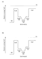
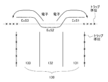
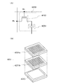
図1(A)、(B)、(C)は、本発明の一態様のトランジスタの上面図および断面図である。図1(A)は上面図であり、図1(A)に示す一点鎖線A1−A2の断面が図1(B)に相当する。また、図1(A)に示す一点鎖線A3−A4の断面が図1(C)に相当する。なお、図1(A)の上面図では、図の明瞭化のために一部の要素を省いて図示している。また、一点鎖線A1−A2方向をチャネル幅方向、一点鎖線A3−A4方向をチャネル長方向と呼称する場合がある。 1A, 1B, and 1C are a top view and cross-sectional views of a transistor of one embodiment of the present invention. FIG. 1A is a top view, and a cross section taken along dashed-dotted line A1-A2 in FIG. 1A corresponds to FIG. A cross section taken along alternate long and short dash line A3-A4 in FIG. 1A corresponds to FIG. Note that in the top view of FIG. 1A, some elements are omitted for clarity. The direction of the alternate long and short dash line A1-A2 may be referred to as a channel width direction, and the direction of the alternate long and short dash line A3-A4 may be referred to as a channel length direction.
図1(A)、(B)、(C)に示すトランジスタ100は、基板110上に形成された下地絶縁膜120、該下地絶縁膜120上に形成された酸化物半導体層130、該酸化物半導体層130上に形成されたソース電極層140、ドレイン電極層150、該ソース電極層140、該ドレイン電極層150、および酸化物半導体層130上に形成されたゲート絶縁膜160、該ゲート絶縁膜160上に形成された第1のゲート電極層171、第2のゲート電極層172、第3のゲート電極層173を有する。また、該ゲート絶縁膜160および該第1のゲート電極層171、第2のゲート電極層172、第3のゲート電極層173上に酸化物絶縁層180が形成されていてもよい。当該酸化物絶縁層180は必要に応じて設ければよく、さらにその上部に他の絶縁層を形成してもよい。
1A, 1B, and 1C includes a
なお、トランジスタの「ソース」や「ドレイン」の機能は、異なる極性のトランジスタを採用する場合や、回路動作において電流の方向が変化する場合などには入れ替わることがある。このため、本明細書においては、「ソース」や「ドレイン」の用語は、入れ替えて用いることができるものとする。 Note that the functions of the “source” and “drain” of the transistor may be interchanged when a transistor with a different polarity is used or when the direction of current changes during circuit operation. Therefore, in this specification, the terms “source” and “drain” can be used interchangeably.
基板110は、単なる支持基板に限らず、他のトランジスタなどのデバイスが形成された基板であってもよい。この場合、トランジスタ100の第1のゲート電極層171、第2のゲート電極層172、第3のゲート電極層173、ソース電極層140、およびドレイン電極層150の少なくとも一つは、上記の他のデバイスと電気的に接続されていてもよい。
The
下地絶縁膜120は、基板110からの不純物の拡散を防止する役割を有するほか、酸化物半導体層130に酸素を供給する役割を担うことができるため、酸素を含む絶縁膜であることが好ましく、過剰な酸素を含む絶縁膜がより好ましい。また、上述のように基板110が他のデバイスが形成された基板である場合、下地絶縁膜120は、層間絶縁膜としての機能も有する。その場合は、表面が平坦になるようにCMP(Chemical Mechanical Polishing)法等で平坦化処理を行うことが好ましい。
The base
酸化物半導体層130は、基板110側から第1の酸化物半導体層131、第2の酸化物半導体層132、第3の酸化物半導体層133が積層された構造を有している。ここで、第2の酸化物半導体層132には、第1の酸化物半導体層131および第3の酸化物半導体層133よりも電子親和力(真空準位から伝導帯下端までのエネルギー)が大きい酸化物半導体を用いる。電子親和力は、真空準位と価電子帯上端とのエネルギー差(イオン化ポテンシャル)から、伝導帯下端と価電子帯上端とのエネルギー差(バンドギャップ)を差し引いた値として求めることができる。
The
なお、本実施の形態では、酸化物半導体層130が三層の積層である場合について説明するが、酸化物半導体層130が一層、二層または四層以上であってもよい。一層の場合は、第2の酸化物半導体層132に相当する層を用いればよい。二層の場合は、基板110側に第2の酸化物半導体層132に相当する層を用い、ゲート絶縁膜160側に第1の酸化物半導体層131または第3の酸化物半導体層133に相当する層を用いればよい。四層以上である場合は、本実施の形態の説明と同じように第2の酸化物半導体層132が第1の酸化物半導体層131または第3の酸化物半導体層133に相当する層で挟まれる構造とすればよい。
Note that although the case where the
第1の酸化物半導体層131および第3の酸化物半導体層133は、第2の酸化物半導体層132を構成する金属元素を一種以上含み、伝導帯下端のエネルギーが第2の酸化物半導体層132よりも、0.05eV、0.07eV、0.1eV、0.15eVのいずれか以上であって、2eV、1eV、0.5eV、0.4eVのいずれか以下の範囲で真空準位に近い酸化物半導体で形成することが好ましい。
The first
このような構造において、第1のゲート電極層171に電界を印加すると、酸化物半導体層130のうち、伝導帯下端のエネルギーが最も小さい第2の酸化物半導体層132にチャネルが形成される。すなわち、第2の酸化物半導体層132とゲート絶縁膜160との間に第3の酸化物半導体層133が形成されていることよって、トランジスタのチャネルをゲート絶縁膜160と接しない構造とすることができる。
In such a structure, when an electric field is applied to the first
また、第2の酸化物半導体層132を構成する金属元素を一種以上含んで第1の酸化物半導体層131が構成されるため、第2の酸化物半導体層132と第1の酸化物半導体層131の界面に界面準位を形成しにくくなる。該界面準位はチャネルを形成することがあるため、しきい値電圧の異なる第2のトランジスタが出現し、トランジスタの見かけ上のしきい値電圧が変動することがある。したがって、第1の酸化物半導体層131を設けることにより、トランジスタのしきい値電圧などの電気特性のばらつきを低減することができる。
In addition, since the first
また、第2の酸化物半導体層132を構成する金属元素を一種以上含んで第3の酸化物半導体層133が構成されるため、第2の酸化物半導体層132と第3の酸化物半導体層133との界面ではキャリアの散乱が起こりにくくなる。したがって、第3の酸化物半導体層133を設けることにより、トランジスタの電界効果移動度を高くすることができる。
In addition, since the third
第1の酸化物半導体層131および第3の酸化物半導体層133には、例えば、Al、Ti、Ga、Ge、Y、Zr、Sn、La、CeまたはHfを第2の酸化物半導体層132よりも高い原子数比で含む材料を用いることができる。具体的には、当該原子数比を1.5倍以上、好ましくは2倍以上、さらに好ましくは3倍以上とする。前述の元素は酸素と強く結合するため、酸素欠損が酸化物半導体層に生じることを抑制する機能を有する。すなわち、第1の酸化物半導体層131および第3の酸化物半導体層133は、第2の酸化物半導体層132よりも酸素欠損が生じにくいということができる。
For the first
なお、第1の酸化物半導体層131、第2の酸化物半導体層132、第3の酸化物半導体層133が、少なくともインジウム、亜鉛およびM(Al、Ti、Ga、Ge、Y、Zr、Sn、La、CeまたはHf等の金属)を含むIn−M−Zn酸化物であるとき、第1の酸化物半導体層131をIn:M:Zn=x1:y1:z1[原子数比]、第2の酸化物半導体層132をIn:M:Zn=x2:y2:z2[原子数比]、第3の酸化物半導体層133をIn:M:Zn=x3:y3:z3[原子数比]とすると、y1/x1およびy3/x3がy2/x2よりも大きくなることが好ましい。y1/x1およびy3/x3はy2/x2よりも1.5倍以上、好ましくは2倍以上、さらに好ましくは3倍以上とする。このとき、第2の酸化物半導体層132において、y2がx2以上であるとトランジスタの電気特性を安定させることができる。ただし、y2がx2の3倍以上になると、トランジスタの電界効果移動度が低下してしまうため、y2はx2の3倍未満であることが好ましい。
Note that the first
また、第1の酸化物半導体層131および第3の酸化物半導体層133のInとMの原子数比率は、好ましくはInが50atomic%未満、Mが50atomic%以上、さらに好ましくはInが25atomic%未満、Mが75atomic%以上とする。また、第2の酸化物半導体層132のInとMの原子数比率は、好ましくはInが25atomic%以上、Mが75atomic%未満、さらに好ましくはInが34atomic%以上、Mが66atomic%未満とする。
The atomic ratio of In and M in the first
第1の酸化物半導体層131および第3の酸化物半導体層133の厚さは、3nm以上100nm以下、好ましくは3nm以上50nm以下とする。また、第2の酸化物半導体層132の厚さは、3nm以上200nm以下、好ましくは3nm以上100nm以下、さらに好ましくは3nm以上50nm以下とする。
The thicknesses of the first
第1の酸化物半導体層131、第2の酸化物半導体層132、および第3の酸化物半導体層133には、例えば、インジウム、亜鉛およびガリウムを含んだ酸化物半導体を用いることができる。特に、第2の酸化物半導体層132にインジウムを含ませると、キャリア移動度が高くなるため好ましい。
For the first
なお、酸化物半導体層をチャネルとするトランジスタに安定した電気特性を付与するためには、酸化物半導体層中の不純物濃度を低減し、酸化物半導体層を真性または実質的に真性にすることが有効である。ここで、実質的に真性とは、酸化物半導体層のキャリア密度が、1×10¹⁷/cm3未満であること、好ましくは1×1015/cm3未満であること、さらに好ましくは1×1013/cm3未満であることを指す。 Note that in order to impart stable electric characteristics to the transistor including the oxide semiconductor layer as a channel, the impurity concentration in the oxide semiconductor layer is reduced so that the oxide semiconductor layer is intrinsic or substantially intrinsic. It is valid. Here, substantially intrinsic means that the carrier density of the oxide semiconductor layer is less than 1 × 10 17 / cm 3 , preferably less than 1 × 10 15 / cm 3 , and more preferably 1 × It indicates less than 10 13 / cm 3 .
また、酸化物半導体層において、水素、窒素、炭素、シリコン、および主成分以外の金属元素は不純物となる。例えば、水素および窒素は、ドナー準位の形成に寄与し、キャリア密度を増大させてしまう。また、シリコンは、酸化物半導体層中で不純物準位を形成する。当該不純物準位はトラップとなり、トランジスタの電気特性を劣化させることがある。したがって、第1の酸化物半導体層131、第2の酸化物半導体層132および第3の酸化物半導体層133の層中や、それぞれの界面において不純物濃度を低減させることが有効である。
In the oxide semiconductor layer, hydrogen, nitrogen, carbon, silicon, and a metal element other than the main component are impurities. For example, hydrogen and nitrogen contribute to the formation of donor levels and increase the carrier density. Silicon forms impurity levels in the oxide semiconductor layer. The impurity level becomes a trap and may deteriorate the electrical characteristics of the transistor. Therefore, it is effective to reduce the impurity concentration in the layers of the first
酸化物半導体層を真性または実質的に真性とするためには、SIMS(Secondary Ion Mass Spectrometry)分析において、シリコン濃度を1×10¹⁹atoms/cm3未満、好ましくは5×1018atoms/cm3未満、さらに好ましくは1×1018atoms/cm3未満とする。また、水素濃度は、2×1020atoms/cm3以下、好ましくは5×1019atoms/cm3以下、より好ましくは1×1019atoms/cm3以下、さらに好ましくは5×1018atoms/cm3以下とする。また、窒素濃度は、5×1019atoms/cm3未満、好ましくは5×1018atoms/cm3以下、より好ましくは1×1018atoms/cm3以下、さらに好ましくは5×1017atoms/cm3以下とする。 In order to make the oxide semiconductor layer intrinsic or substantially intrinsic, a silicon concentration is less than 1 × 10 19 atoms / cm 3 , preferably 5 × 10 18 atoms / cm 3 in a SIMS (Secondary Ion Mass Spectrometry) analysis. Less than, more preferably less than 1 × 10 18 atoms / cm 3 . The hydrogen concentration is 2 × 10 20 atoms / cm 3 or less, preferably 5 × 10 19 atoms / cm 3 or less, more preferably 1 × 10 19 atoms / cm 3 or less, and even more preferably 5 × 10 18 atoms / cm 3. cm 3 or less. The nitrogen concentration is less than 5 × 10 19 atoms / cm 3 , preferably 5 × 10 18 atoms / cm 3 or less, more preferably 1 × 10 18 atoms / cm 3 or less, and further preferably 5 × 10 17 atoms / cm 3. cm 3 or less.
また、酸化物半導体層が結晶を含む場合、シリコンや炭素が高濃度で含まれると、酸化物半導体層の結晶性を低下させることがある。酸化物半導体層の結晶性を低下させないためには、シリコン濃度を1×10¹⁹atoms/cm3未満、好ましくは5×1018atoms/cm3未満、さらに好ましくは1×1018atoms/cm3未満とすればよい。また、炭素濃度を1×1019atoms/cm3未満、好ましくは5×1018atoms/cm3未満、さらに好ましくは1×1018atoms/cm3未満とすればよい。 In addition, in the case where the oxide semiconductor layer includes a crystal, the crystallinity of the oxide semiconductor layer may be reduced if silicon or carbon is included at a high concentration. In order not to reduce the crystallinity of the oxide semiconductor layer, the silicon concentration is less than 1 × 10 19 atoms / cm 3 , preferably less than 5 × 10 18 atoms / cm 3 , more preferably 1 × 10 18 atoms / cm 3. It may be less than. The carbon concentration may be less than 1 × 10 19 atoms / cm 3 , preferably less than 5 × 10 18 atoms / cm 3 , and more preferably less than 1 × 10 18 atoms / cm 3 .
また、上述のように高純度化された酸化物半導体膜をチャネル形成領域に用いたトランジスタのオフ電流は極めて小さく、トランジスタのチャネル幅で規格化したオフ電流は、数yA/μm〜数zA/μmにまで低減することが可能となる。 Further, the off-state current of a transistor using the oxide semiconductor film purified as described above as a channel formation region is extremely small, and the off-state current normalized by the channel width of the transistor ranges from several yA / μm to several zA / It can be reduced to μm.
なお、トランジスタのゲート絶縁膜としては、シリコンを含む絶縁膜が多く用いられるため、上記理由により酸化物半導体層のチャネルとなる領域はゲート絶縁膜と接しないことが好ましいということができる。また、ゲート絶縁膜と酸化物半導体層との界面にチャネルが形成される場合、該界面でキャリアの散乱が起こり、トランジスタの電界効果移動度が低くなることがある。このような観点からも、酸化物半導体層のチャネルとなる領域はゲート絶縁膜から離すことが好ましい。 Note that since an insulating film containing silicon is often used as a gate insulating film of a transistor, it can be said that a region serving as a channel of an oxide semiconductor layer is preferably not in contact with the gate insulating film for the above reason. In addition, in the case where a channel is formed at the interface between the gate insulating film and the oxide semiconductor layer, carrier scattering occurs at the interface, and the field-effect mobility of the transistor may be reduced. From this point of view, it is preferable that the region serving as the channel of the oxide semiconductor layer be separated from the gate insulating film.
したがって、酸化物半導体層130を第1の酸化物半導体層131、第2の酸化物半導体層132、第3の酸化物半導体層133の積層構造とすることで、トランジスタのチャネルが形成される第2の酸化物半導体層132をゲート絶縁膜から離すことができ、高い電界効果移動度を有し、安定した電気特性のトランジスタを形成することができる。
Therefore, the
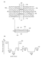
次に、酸化物半導体層130のバンド構造を説明する。バンド構造の解析は、第1の酸化物半導体層131および第3の酸化物半導体層133に相当する層としてエネルギーギャップが3.15eVであるIn−Ga−Zn酸化物、第2の酸化物半導体層132に相当する層としてエネルギーギャップが2.8eVであるIn−Ga−Zn酸化物を用い、酸化物半導体層130に相当する積層を作製して行っている。なお、便宜的に当該積層を酸化物半導体層130、当該積層を構成するそれぞれの層を第1の酸化物半導体層131、第2の酸化物半導体層132、第3の酸化物半導体層133と称して説明する。
Next, a band structure of the
第1の酸化物半導体層131、第2の酸化物半導体層132、第3の酸化物半導体層133の膜厚はそれぞれ10nmとし、エネルギーギャップは、分光エリプソメータ(HORIBA JOBIN YVON社 UT−300)を用いて測定した。また、第1の酸化物半導体層131と第2の酸化物半導体層132との界面近傍のエネルギーギャップは3eV、第3の酸化物半導体層133と第2の酸化物半導体層132との界面近傍のエネルギーギャップは3eVとした。
The film thicknesses of the first
図2(A)は、酸化物半導体層130を第3の酸化物半導体層133からエッチングしつつ、各層の真空準位と価電子帯上端のエネルギー差を測定し、その値をプロットした図である。真空準位と価電子帯上端のエネルギー差は、紫外線光電子分光分析(UPS:Ultraviolet Photoelectron Spectroscopy)装置(PHI社 VersaProbe)を用いて測定した。
FIG. 2A is a diagram in which the energy difference between the vacuum level and the valence band top of each layer is measured while the
図2(B)は、真空準位と価電子帯上端のエネルギー差と、各層のエネルギーギャップとの差分として算出される真空準位と伝導帯下端のエネルギー差(電子親和力)をプロットした図である。 FIG. 2B is a graph plotting the energy difference (electron affinity) between the vacuum level and the conduction band bottom calculated as the difference between the energy difference between the vacuum level and the top of the valence band and the energy gap of each layer. is there.
そして、図2(B)を模式的に示したバンド構造の一部が、図3(A)である。図3(A)では、第1の酸化物半導体層131および第3の酸化物半導体層133と接して、酸化シリコン膜を設けた場合について説明する。ここで、Evは真空準位のエネルギー、EcI1およびEcI2は酸化シリコン膜の伝導帯下端のエネルギー、EcS1は第1の酸化物半導体層131の伝導帯下端のエネルギー、EcS2は第2の酸化物半導体層132の伝導帯下端のエネルギー、EcS3は第3の酸化物半導体層133の伝導帯下端のエネルギーを示す。また、トランジスタを構成する場合、ゲート電極層(トランジスタ100では第1のゲート電極層171に相当)はEcI2を有する酸化シリコン膜に接するものとする。
A part of the band structure schematically showing FIG. 2B is FIG. 3A illustrates the case where a silicon oxide film is provided in contact with the first
図3(A)に示すように、第1の酸化物半導体層131、第2の酸化物半導体層132、第3の酸化物半導体層133において、伝導帯下端のエネルギーが連続的に変化する。これは、第1の酸化物半導体層131、第2の酸化物半導体層132、第3の酸化物半導体層133の組成が近似することにより、酸素が相互に拡散しやすい点からも理解される。
As shown in FIG. 3A, in the first
主成分を共通として積層された酸化物半導体層130は、各層を単に積層するのではなく連続接合(ここでは特に伝導帯下端のエネルギーが各層の間で連続的に変化するU字型の井戸構造)が形成されるように作製する。すなわち、各層の界面に酸化物半導体にとってトラップ中心や再結合中心のような欠陥準位、あるいはキャリアの流れを阻害するバリアを形成するような不純物が存在しないように積層構造を形成する。仮に、積層された酸化物半導体層の層間に不純物が混在していると、エネルギーバンドの連続性が失われ、界面でキャリアがトラップあるいは再結合により消滅してしまう。
The
連続接合を形成するためには、ロードロック室を備えたマルチチャンバー方式の成膜装置(スパッタ装置)を用いて各層を大気に触れさせることなく連続して積層することが必要となる。スパッタ装置における各チャンバーは、酸化物半導体にとって不純物となる水等を可能な限り除去すべく、クライオポンプのような吸着式の真空排気ポンプを用いて高真空排気(1×10⁻⁴Pa〜5×10⁻⁷Pa程度まで)できること、かつ、成膜される基板を100℃以上に加熱できることが好ましい。または、ターボ分子ポンプとコールドトラップを組み合わせて排気系からチャンバー内に炭素成分や水分等を含む気体が逆流しないようにしておくことが好ましい。 In order to form a continuous bond, it is necessary to use a multi-chamber type film forming apparatus (sputtering apparatus) having a load lock chamber to successively laminate each layer without exposure to the atmosphere. Each chamber in the sputtering apparatus is subjected to high vacuum exhaust (1 × 10 −4 Pa to 5 × 5) using an adsorption-type vacuum exhaust pump such as a cryopump in order to remove as much as possible water which is an impurity for the oxide semiconductor. × 10 -7 Pa to about) can be, and is preferably capable of heating the substrate to be deposited over 100 ° C.. Alternatively, it is preferable to combine a turbo molecular pump and a cold trap so that a gas containing a carbon component or moisture does not flow backward from the exhaust system into the chamber.
高純度真性酸化物半導体を得るためには、チャンバー内を高真空排気するのみならずスパッタガスの高純度化も必要である。スパッタガスとして用いる酸素ガスやアルゴンガスは、露点が−40℃以下、好ましくは−80℃以下、より好ましくは−100℃以下にまで高純度化したガスを用いることで酸化物半導体膜に水分等が取り込まれることを可能な限り防ぐことができる。 In order to obtain a high-purity intrinsic oxide semiconductor, it is necessary not only to evacuate the chamber to a high vacuum but also to increase the purity of the sputtering gas. Oxygen gas or argon gas used as a sputtering gas has a dew point of −40 ° C. or lower, preferably −80 ° C. or lower, more preferably −100 ° C. or lower. Can be prevented as much as possible.
なお、図3(A)では、EcS1とEcS3が同様である場合について示したが、それぞれが異なっていてもよい。例えば、EcS3よりもEcS1が高いエネルギーを有する場合、バンド構造の一部は、図3(B)のように示される。 Note that although FIG. 3A illustrates the case where EcS1 and EcS3 are the same, they may be different from each other. For example, when EcS1 has higher energy than EcS3, a part of the band structure is shown as in FIG.
例えば、EcS1=EcS3である場合は、第1の酸化物半導体層131および第3の酸化物半導体層133にIn:Ga:Zn=1:3:2(原子数比)、第2の酸化物半導体層132にIn:Ga:Zn=1:1:1(原子数比)のIn−Ga−Zn酸化物などを用いることができる。また、EcS1>EcS3である場合は、第1の酸化物半導体層131にIn:Ga:Zn=1:6:4または1:9:6(原子数比)、第2の酸化物半導体層132にIn:Ga:Zn=1:1:1または3:1:2(原子数比)、第3の酸化物半導体層133にIn:Ga:Zn=1:3:2(原子数比)のIn−Ga−Zn酸化物などを用いることができる。
For example, when EcS1 = EcS3, the first
図2(A)、(B)および図3(A)、(B)より、酸化物半導体層130における第2の酸化物半導体層132がウェル(井戸)となり、酸化物半導体層130を用いたトランジスタにおいて、チャネルが第2の酸化物半導体層132に形成されることがわかる。なお、酸化物半導体層130は伝導帯下端のエネルギーが連続的に変化しているため、U字型井戸(U Shape Well)とも呼ぶことができる。また、このような構成で形成されたチャネルを埋め込みチャネルということもできる。
2A and 2B and FIGS. 3A and 3B, the second
なお、図4に示すように、第1の酸化物半導体層131および第3の酸化物半導体層133と、酸化シリコン膜などの絶縁膜との界面近傍には、不純物や欠陥に起因したトラップ準位が形成され得る。第1の酸化物半導体層131および第3の酸化物半導体層133があることにより、第2の酸化物半導体層132と当該トラップ準位とを遠ざけることができる。ただし、EcS1またはEcS3と、EcS2とのエネルギー差が小さい場合、第2の酸化物半導体層132の電子が該エネルギー差を超えてトラップ準位に達することがある。トラップ準位に電子が捕獲されることで、絶縁膜界面にマイナスの固定電荷が生じ、トランジスタのしきい値電圧はプラス方向にシフトしてしまう。
Note that as illustrated in FIG. 4, in the vicinity of the interface between the first
したがって、EcS1およびEcS3と、EcS2とのエネルギー差を、それぞれ0.1eV以上、好ましくは0.15eV以上とすることで、トランジスタのしきい値電圧の変動が低減され、安定した電気特性を得ることができる。 Therefore, by setting the energy difference between EcS1 and EcS3 and EcS2 to 0.1 eV or more, preferably 0.15 eV or more, variation in the threshold voltage of the transistor is reduced, and stable electrical characteristics can be obtained. Can do.
なお、第1の酸化物半導体層131、第2の酸化物半導体層132および第3の酸化物半導体層133のいずれか一つ以上の層には、結晶部が含まれることが好ましい。例えば、第1の酸化物半導体層131を非晶質とし、第2の酸化物半導体層132および第3の酸化物半導体層133を結晶部が含まれる層とする。チャネルが形成される第2の酸化物半導体層132が結晶部を含むことにより、トランジスタに安定した電気特性を付与することができる。
Note that at least one of the first
特に、第2の酸化物半導体層132および第3の酸化物半導体層133に含まれる結晶部は、表面と略垂直な方向にc軸が配向した結晶を有することが好ましい。
In particular, the crystal part included in the second
また、図1の構造のトランジスタにおいて、第3の酸化物半導体層133はソース電極層140およびドレイン電極層150に接しており、電流を効率良く取り出すにはエネルギーギャップが絶縁体のように大きくないこと、および膜厚が薄いことが好ましい。また、酸化物半導体層130にIn−Ga−Zn酸化物を用いる場合は、Inのゲート絶縁膜への拡散を防ぐために、第3の酸化物半導体層133は第2の酸化物半導体層132よりもInを少なくする組成とすることが好ましい。
In the transistor having the structure illustrated in FIGS. 1A and 1B, the third
また、図5(A)のトランジスタの拡大図に示すように、酸化物半導体層130の端部に曲面を有する領域134を設けても良い。酸化物半導体層130をIn−M−Zn酸化物(MはAl、Ti、Ga、Y、Zr、La、Ce、NdまたはHf)で形成する場合、第2の酸化物半導体層132を構成するM(MS2)と領域134を構成するM(MS4)の量的関係は、MS4>MS2であることが好ましい。より好ましくは、MS4は第1の酸化物半導体層131を構成するM(MS1)と同等とする。
Further, as illustrated in the enlarged view of the transistor in FIG. 5A, a
酸化物半導体層130の端部における領域134は、ドライエッチング法にて第1の酸化物半導体層131の成分を第2の酸化物半導体層132及び第3の酸化物半導体層133に再付着させる、所謂ラビットイヤーを利用して形成することができる。さらに酸化処理によりラビットイヤー形成時に付着するエッチングガス成分を除去し、M成分を酸化することで領域134の絶縁性を高めることができる。
In the
また、図5(B)に示すように酸化物半導体層130をドライエッチングする際に、下地絶縁膜120の一部がエッチングされる。このため、酸化物半導体層130が接する領域の下地絶縁膜120の膜厚は、酸化物半導体層130が接しない領域の下地絶縁膜120の膜厚より大きい。このような構成になることで、酸化物半導体層130と、ソース電極層140またはドレイン電極層150との密着性を向上させることができる。
In addition, when the
図6(A)は図1に示すトランジスタの上面図および酸化物半導体層130の断面図である。ゲート電極層が重畳する酸化物半導体層130の領域134は、外的要因による不純物の混入や酸素欠損の発生などによりn型化しやすく、寄生チャネルとなることがある。特にエネルギーギャップの小さい第2の酸化物半導体層132ではn型化が顕著に起こりやすいため、第2の酸化物半導体層132を覆う領域134には寄生チャネルの発生を抑制する作用があるといえる。
6A is a top view of the transistor illustrated in FIG. 1 and a cross-sectional view of the
第1の酸化物半導体層131と領域134の主成分が同一であるとき、第2の酸化物半導体層132の伝導帯下端のエネルギー(EcS2)と領域134の伝導帯下端のエネルギー(EcS4)の差分(ΔE)が大きいほど寄生チャネルの発生を抑える効果が高い。また、領域134の厚みは、第1の酸化物半導体層131または第3の酸化物半導体層133よりも厚いことが好ましく、厚いほど第2の酸化物半導体層132端部のn型化による寄生チャネルの発生を抑えることができる。
When the main components of the first
また、領域134は、第1の酸化物半導体層131、第2の酸化物半導体層132、第3の酸化物半導体層133と組成が近似することにより、酸化物半導体層130のバンド構造の一部を示す図6(B)のように伝導帯下端のエネルギーが連続的に変化する。すなわち、第1の酸化物半導体層131、第2の酸化物半導体層132、第3の酸化物半導体層133、および領域134は連続接合であるということができる。なお、図6(B)に示す一点鎖線D1−D2は、図6(A)の酸化物半導体層130の断面図に示す一点鎖線D1−D2方向に相当し、図6(B)に示すE1−E2は図6(A)に示す一点鎖線E1−E2方向に相当する。
The
ソース電極層140およびドレイン電極層150には、酸素と結合し易い導電材料を用いることができる。例えば、Al、Cr、Cu、Ta、Ti、Mo、Wなどを用いることができる。後のプロセス温度が比較的高くできることなどから、融点の高いWを用いることが特に好ましい。なお、酸素と結合し易い導電材料には、酸素が拡散し易い材料も含まれる。
The
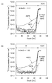
酸素と結合し易い導電材料と酸化物半導体層を接触させると、酸化物半導体層中の酸素が、酸素と結合し易い導電材料側に拡散する現象が起こる。例えば、図19(A)、(B)はスパッタ法でIn−Ga−Zn酸化物膜(以降、IGZO膜ともいう)およびタングステン膜の積層サンプルを形成し、酸素同位体(18O)の深さ方向のプロファイルを熱処理前後でSIMS分析した結果である。なお、IGZO膜はIn:Ga:Zn=1:1:1または1:3:2(原子数比)をスパッタターゲットとし、Ar:O2(18O)=2:1(流量比)をスパッタガスとして用いてDCスパッタ法で形成している。また、タングステン膜は、金属Wをスパッタターゲットとし、Ar100%をスパッタガスとしてDCスパッタ法で形成している。なお、熱処理は、300℃、350℃、400℃、450℃の各1時間で行い、熱処理無しサンプルを含めて計5サンプルで比較を行った。図19に示すように、熱処理温度が高くなると酸化物半導体層中の酸素がタングステン膜に拡散していることがわかる。
When the conductive material that is easily bonded to oxygen and the oxide semiconductor layer are brought into contact with each other, a phenomenon occurs in which oxygen in the oxide semiconductor layer diffuses toward the conductive material that is easily bonded to oxygen. For example, in FIGS. 19A and 19B, a stacked sample of an In—Ga—Zn oxide film (hereinafter also referred to as an IGZO film) and a tungsten film is formed by sputtering, and the depth of oxygen isotope ( 18 O) is increased. It is a result of SIMS analysis of the profile in the vertical direction before and after heat treatment. The IGZO film was sputtered with In: Ga: Zn = 1: 1: 1 or 1: 3: 2 (atomic ratio) and Ar: O 2 ( 18 O) = 2: 1 (flow ratio). It is formed by DC sputtering using as a gas. The tungsten film is formed by DC sputtering using metal W as a sputtering target and
トランジスタの作製工程には、いくつかの加熱工程があることから、上記現象により、酸化物半導体層のソース電極層およびドレイン電極層と接触した近傍の領域に酸素欠損が発生し、当該領域はn型化する。したがって、n型化した当該領域はトランジスタのソースまたはドレインとして作用させることができる。 Since there are several heating steps in the manufacturing process of the transistor, oxygen vacancies are generated in a region in contact with the source electrode layer and the drain electrode layer of the oxide semiconductor layer due to the above phenomenon. Type. Therefore, the n-type region can serve as the source or drain of the transistor.
しかしながら、チャネル長が極短いトランジスタを形成する場合、上記酸素欠損の発生によってn型化した領域がトランジスタのチャネル長方向に延在してしまうことがある。この場合、トランジスタの電気特性には、しきい値電圧のシフトやゲート電圧でオンオフの制御ができない状態(導通状態)が現れる。そのため、チャネル長が極短いトランジスタを形成する場合は、ソース電極層およびドレイン電極層に酸素と結合し易い導電材料を用いることは好ましくない。 However, in the case of forming a transistor with an extremely short channel length, the n-type region due to the generation of oxygen vacancies may extend in the channel length direction of the transistor. In this case, a state (conduction state) in which on / off cannot be controlled by a threshold voltage shift or a gate voltage appears in the electrical characteristics of the transistor. Therefore, in the case of forming a transistor with an extremely short channel length, it is not preferable to use a conductive material that easily binds to oxygen for the source electrode layer and the drain electrode layer.
したがって、図7(A)、(B)、(C)に示すトランジスタ101のようにソース電極層およびドレイン電極層を積層としてもよい。図7(A)は上面図であり、図7(A)に示す一点鎖線B1−B2の断面が図7(B)に相当する。また、図7(A)に示す一点鎖線B3−B4の断面が図7(C)に相当する。また、一点鎖線B1−B2方向をチャネル幅方向、一点鎖線B3−B4方向をチャネル長方向と呼称する場合がある。第1のソース電極層141および第1のドレイン電極層151には、上述したタングステン膜を用い、チャネル長を定める第2のソース電極層142および第2のドレイン電極層152には、酸素と結合しにくい導電材料を用いる。当該導電材料としては、例えば、窒化タンタル、窒化チタン、ルテニウムなどを用いることが好ましい。なお、酸素と結合しにくい導電材料には、酸素が拡散しにくい材料も含まれる。
Therefore, a source electrode layer and a drain electrode layer may be stacked as in the
図20(A)、(B)はスパッタ法でIGZO膜および窒化タンタル膜の積層サンプルを形成し、酸素同位体(18O)の深さ方向のプロファイルを熱処理前後でSIMS分析した結果である。また、図21(A)、(B)はスパッタ法でIGZO膜および窒化チタン膜の積層サンプルを形成し、酸素同位体(18O)の深さ方向のプロファイルを熱処理前後でSIMS分析した結果である。 20A and 20B show the results of SIMS analysis of the oxygen isotope ( 18 O) depth profile before and after the heat treatment by forming a laminated sample of an IGZO film and a tantalum nitride film by sputtering. 21A and 21B show the results of SIMS analysis of the oxygen isotope ( 18 O) depth profile before and after the heat treatment by forming a laminated sample of an IGZO film and a titanium nitride film by sputtering. is there.
IGZO膜はIn:Ga:Zn=1:1:1または1:3:2(原子数比)をスパッタターゲットとし、Ar:O2(18O)=2:1(流量比)をスパッタガスとして用いてDCスパッタ法で形成している。また、窒化タンタル膜は、金属Taをスパッタターゲットとし、Ar:N2=5:1(流量比)をスパッタガスとして反応性スパッタ法(DCスパッタ法)で形成し、窒化チタン膜は、金属Tiをスパッタターゲットとし、N2100%をスパッタガスとして反応性スパッタ法(DCスパッタ法)で形成している。なお、熱処理は、300℃、350℃、400℃、450℃の各1時間で行い、熱処理無しサンプルを含めて計5サンプルで比較を行っている。
The IGZO film uses In: Ga: Zn = 1: 1: 1 or 1: 3: 2 (atomic ratio) as a sputtering target, and Ar: O 2 ( 18 O) = 2: 1 (flow ratio) as a sputtering gas. And formed by DC sputtering. The tantalum nitride film is formed by reactive sputtering (DC sputtering) using metal Ta as a sputtering target and Ar: N 2 = 5: 1 (flow rate ratio) as sputtering gas, and the titanium nitride film is formed from metal Ti Is formed by a reactive sputtering method (DC sputtering method) using
いずれのサンプルにおいても、窒化タンタル中または窒化チタン膜中への酸素拡散は確認されず、図19(A)、(B)に示したタングステン膜を用いたサンプルとは異なった挙動を示した。したがって、窒化タンタル膜および窒化チタン膜は酸素と結合しにくい膜、または酸素が拡散しにくい膜ということができる。 In any of the samples, oxygen diffusion into the tantalum nitride or the titanium nitride film was not confirmed, and the behavior was different from the sample using the tungsten film shown in FIGS. Therefore, the tantalum nitride film and the titanium nitride film can be referred to as films that are difficult to bond to oxygen or films from which oxygen is difficult to diffuse.
なお、図7の構造のトランジスタにおいて、チャネル長とは、第2のソース電極層142と第2のドレイン電極層152の間隔のことをいう。
Note that in the transistor having the structure in FIG. 7, the channel length refers to the distance between the second
また、図7の構造のトランジスタにおいて、チャネルとは、第2のソース電極層142と第2のドレイン電極層152の間における第2の酸化物半導体層132のことをいう。
In the transistor having the structure in FIG. 7, a channel refers to the second
また、図7の構造のトランジスタにおいて、チャネル形成領域とは、第2のソース電極層142と第2のドレイン電極層152の間における第1の酸化物半導体層131、第2の酸化物半導体層132、第3の酸化物半導体層133のことをいう。
In the transistor having the structure in FIG. 7, the channel formation region refers to the first
上記酸素と結合しにくい導電材料を第2のソース電極層142および第2のドレイン電極層152に用いることによって、酸化物半導体層に形成されるチャネル形成領域に酸素欠損が形成されることを抑制することができ、チャネルのn型化を抑えることができる。したがって、チャネル長が極短いトランジスタであっても良好な電気特性を得ることができる。
By using the conductive material that is difficult to bond to oxygen for the second
なお、上記酸素と結合しにくい導電材料のみでソース電極層およびドレイン電極層を形成すると、酸化物半導体層130とのコンタクト抵抗が高くなりすぎることから、図7(C)に示すように、第1のソース電極層141および第1のドレイン電極層151を酸化物半導体層130上に形成し、第1のソース電極層141および第1のドレイン電極層151を覆うように第2のソース電極層142および第2のドレイン電極層152を形成することが好ましい。
Note that when the source electrode layer and the drain electrode layer are formed using only a conductive material that is difficult to bond to oxygen, the contact resistance with the
このとき、第1のソース電極層141および第1のドレイン電極層151と酸化物半導体層130との接触面積を大として、第2のソース電極層142および第2のドレイン電極層152と酸化物半導体層130との接触面積は小とすることが好ましい。第1のソース電極層141および第1のドレイン電極層151と酸化物半導体層130の接触した領域は、酸素欠損の生成によってn型化した領域となる。該n型化した領域により第1のソース電極層141および第1のドレイン電極層151と酸化物半導体層130のコンタクト抵抗を下げることができる。したがって、第1のソース電極層141および第1のドレイン電極層151と酸化物半導体層130の接触面積を大とすることで、n型化した領域の面積も大とすることが可能となる。
At this time, the contact area between the first
ただし、第2のソース電極層142および第2のドレイン電極層152に窒化タンタルや窒化チタンなどの窒化物を用いる場合は第1のソース電極層141および第1のドレイン電極層151と酸化物半導体層130との接触面積を大とする必要はない。窒化物中の窒素が酸化物半導体層130との界面近傍に僅かに拡散し、酸化物半導体層130中で窒素がドナーとして作用してn型領域を形成し、コンタクト抵抗を低下させることができる。
However, in the case where a nitride such as tantalum nitride or titanium nitride is used for the second
ここで、第1のソース電極層141と第1のドレイン電極層151との間隔L1は、0.8μm以上、好ましくは1.0μm以上とする。L1が0.8μmより小さいとチャネル形成領域において発生する酸素欠損の影響を排除できなくなり、トランジスタの電気特性が低下してしまう。
Here, the distance L1 between the first
一方、第2のソース電極層142と第2のドレイン電極層152との間隔L2は、例えば、30nm以下としても良好なトランジスタの電気特性を得ることができる。
On the other hand, good electrical characteristics of the transistor can be obtained even when the distance L2 between the second
また、ゲート−ドレイン間およびゲート−ソース間の寄生容量を小さくし、半導体装置の周波数特性を向上させるため、ゲート電極層とソース電極層またはドレイン電極層とが極力重ならない構造とすることが好ましい。 In addition, in order to reduce the parasitic capacitance between the gate and the drain and between the gate and the source and improve the frequency characteristics of the semiconductor device, it is preferable that the gate electrode layer and the source electrode layer or the drain electrode layer have a structure that does not overlap as much as possible. .
また、図1に示すソース電極層140およびドレイン電極層150の端部、図7に示す第1のソース電極層141および第1のドレイン電極層151の端部は、階段状に複数の段を設けた形状とすることが好ましい。このような複数の段を設けた形状とすることで、それらの上方に形成される膜の被覆性が向上し、トランジスタの電気特性や長期信頼性を向上させることができる。
Further, the end portions of the
ゲート絶縁膜160には、酸化アルミニウム、酸化マグネシウム、酸化シリコン、酸化窒化シリコン、窒化酸化シリコン、窒化シリコン、酸化ガリウム、酸化ゲルマニウム、酸化イットリウム、酸化ジルコニウム、酸化ランタン、酸化ネオジム、酸化ハフニウムおよび酸化タンタルを一種以上含む絶縁膜を用いることができる。また、ゲート絶縁膜160は上記材料の積層であってもよい。
The
第1のゲート電極層171、第2のゲート電極層172、第3のゲート電極層173は、Al、Ti、Cr、Co、Ni、Cu、Y、Zr、Mo、Ru、Ag、TaおよびWなどの導電膜を用いることができる。また、それぞれのゲート電極層は、上記材料の積層であってもよい。
The first
第1のゲート電極層171、第2のゲート電極層172、第3のゲート電極層173は、それぞれ離間しており、第1のゲート電極層171は、ゲート絶縁膜160を介して酸化物半導体層130と重畳し、第2のゲート電極層172は、ゲート絶縁膜160を介して酸化物半導体層130のチャネル幅方向の一方の端部の一部を覆い、第3のゲート電極層173は、ゲート絶縁膜160を介して酸化物半導体層130のチャネル幅方向の他方の端部の一部を覆っている。
The first
低消費電力の半導体装置を形成するには、トランジスタのオフ電流、特にゲート電圧が0V時の電流(Icutともいう)を低減させることが有効である。Icutを低減させる方法としては、トランジスタのゲート電極とは活性層を挟んで逆側に電極を設け、当該電極に適切な電位を供給することによりトランジスタのしきい値電圧を制御する、所謂バックゲート構造が知られている。しかしながら、本発明の一態様のトランジスタのように、活性層が酸化物半導体である場合は、当該酸化物半導体に酸素を供給するための下地絶縁膜として、膜厚の厚い酸化物絶縁層を用いることが適している。そのため、バックゲートの電位を高くしなければならない問題やバックゲートを設けるための工程増加の問題がある。 In order to form a semiconductor device with low power consumption, it is effective to reduce the off-state current of a transistor, particularly the current when the gate voltage is 0 V (also referred to as Icut). As a method of reducing Icut, a so-called back gate is provided in which an electrode is provided on the opposite side of an active layer with respect to the gate electrode of the transistor, and the threshold voltage of the transistor is controlled by supplying an appropriate potential to the electrode. The structure is known. However, in the case where the active layer is an oxide semiconductor as in the transistor of one embodiment of the present invention, a thick oxide insulating layer is used as a base insulating film for supplying oxygen to the oxide semiconductor. Is suitable. Therefore, there are a problem that the potential of the back gate needs to be increased and a problem that the number of processes for providing the back gate increases.
本発明の一態様のトランジスタにおいて、第1のゲート電極層171は、トランジスタのスイッチングを制御し、第2のゲート電極層172および第3のゲート電極層173は、トランジスタのしきい値電圧を制御する。トランジスタの動作において、第1のゲート電極層171にはトランジスタをオンまたはオフする電位が供給され、第2のゲート電極層172および第3のゲート電極層173にはトランジスタのしきい値電圧を制御するための定電位が供給される。第2のゲート電極層172および第3のゲート電極層173には同じ電位が供給されていてもよいし、異なった電位が供給されていてもよい。
In the transistor of one embodiment of the present invention, the first
上記のように、バックゲートと同様の効果を有する第2のゲート電極層172および第3のゲート電極層173を第1のゲート電極層171と同じ膜厚の薄いゲート絶縁膜側に形成することでしきい値電圧を供給するための電位を低下させることができる。また、第1のゲート電極層171、第2のゲート電極層172および第3のゲート電極層173は同時に形成することができ、工程は増加しない。また、下地絶縁膜である酸化物絶縁層を厚く形成することができる。また、第2のゲート電極層172および第3のゲート電極層173の電位が効率良くトランジスタの活性層にかかるようにするため、図5(B)に示すような下地絶縁膜の一部がエッチングされた構造とすることが好ましい。
As described above, the second
したがって、第2のゲート電極層172および第3のゲート電極層173に定電位を供給することでトランジスタのしきい値電圧を制御することができ、Icutを低減させるとともに半導体装置の長期信頼性を向上させることができる。
Therefore, by supplying a constant potential to the second
ゲート絶縁膜160、第1のゲート電極層171、第2のゲート電極層172および第3のゲート電極層173上には酸化物絶縁層180が形成されていてもよい。当該酸化物絶縁層180には、酸化アルミニウム、酸化マグネシウム、酸化シリコン、酸化窒化シリコン、窒化酸化シリコン、窒化シリコン、酸化ガリウム、酸化ゲルマニウム、酸化イットリウム、酸化ジルコニウム、酸化ランタン、酸化ネオジム、酸化ハフニウムおよび酸化タンタルを一種以上含む絶縁膜を用いることができる。また、当該酸化物絶縁層180は上記材料の積層であってもよい。
An
ここで、酸化物絶縁層180は過剰酸素を有することが好ましい。過剰酸素を含む酸化物絶縁層とは、加熱処理などによって酸素を放出することができる酸化物絶縁層をいう。好ましくは、昇温脱離ガス分光法分析にて、酸素原子に換算しての酸素の放出量が1.0×10¹⁹atoms/cm3以上である膜とする。当該酸化物絶縁層180から放出される酸素はゲート絶縁膜160を経由して酸化物半導体層130のチャネル形成領域に拡散させることができることから、不本意に形成された酸素欠損に酸素を補填することができる。したがって、安定したトランジスタの電気特性を得ることができる。
Here, the
以上が本発明の一態様におけるトランジスタである。当該トランジスタは電気特性が良好であり、長期信頼性の高い半導体装置を提供することができる。 The above is the transistor of one embodiment of the present invention. The transistor has favorable electrical characteristics and can provide a semiconductor device with high long-term reliability.
なお、本実施の形態は、本明細書で示す他の実施の形態と適宜組み合わせることができる。 Note that this embodiment can be combined with any of the other embodiments described in this specification as appropriate.
(実施の形態2)
本実施の形態では、実施の形態1で説明したトランジスタとは異なる構造のトランジスタについて説明する。
(Embodiment 2)
In this embodiment, a transistor having a structure different from that of the transistor described in
図8(A)、(B)、(C)は、本発明の一態様のトランジスタの上面図および断面図である。図8(A)は上面図であり、図8(A)に示す一点鎖線C1−C2の断面が図8(B)に相当する。また、図8(A)に示す一点鎖線C3−C4の断面が図8(C)に相当する。なお、図8(A)の上面図では、図の明瞭化のために一部の要素を省いて図示している。また、一点鎖線C1−C2方向をチャネル幅方向、一点鎖線C3−C4方向をチャネル長方向と呼称する場合がある。 8A, 8B, and 8C are a top view and cross-sectional views of a transistor of one embodiment of the present invention. FIG. 8A is a top view, and a cross section taken along dashed-dotted line C1-C2 in FIG. 8A corresponds to FIG. A cross section along dashed-dotted line C3-C4 in FIG. 8A corresponds to FIG. Note that in the top view of FIG. 8A, some elements are omitted for clarity. Further, the direction of the alternate long and short dash line C1-C2 may be referred to as a channel width direction, and the direction of the alternate long and short dash line C3-C4 may be referred to as a channel length direction.
図8(A)、(B)、(C)に示すトランジスタ200は、基板110上に形成された下地絶縁膜120、該下地絶縁膜120上に形成された酸化物半導体層130、該酸化物半導体層130上に形成された第2のソース電極層142、第2のドレイン電極層152、該第2のソース電極層142および該第2のドレイン電極層152のそれぞれの上に形成された第1のソース電極層141、第1のドレイン電極層151、該第1のソース電極層141、該第2のソース電極層142、該第1のドレイン電極層151、該第2のドレイン電極層152、および酸化物半導体層130上に形成されたゲート絶縁膜160、該ゲート絶縁膜160上に形成された第1のゲート電極層171、第2のゲート電極層172、第3のゲート電極層173、該ゲート絶縁膜160、該第1のゲート電極層171、該第2のゲート電極層172および該第3のゲート電極層173上に形成された酸化物絶縁層180を有する。なお、酸化物絶縁層180は必要に応じて設ければよく、さらにその上部に他の絶縁層を形成してもよい。
A
図7(A)、(B)、(C)に示すトランジスタ101と図8(A)、(B)、(C)に示すトランジスタ200とは、第1のソース電極層141と第2のソース電極層142との積層順序、および第1のドレイン電極層151と第2のドレイン電極層152との積層順序が異なり、その他の点では同じである。また、実施の形態1で説明したトランジスタ100またはトランジスタ101と同じようにトランジスタ200は、第1のゲート電極層171、第2のゲート電極層172および第3のゲート電極層173を有している。
The
トランジスタ200では、酸化物半導体層130と、第1のソース電極層141および第1のドレイン電極層151とが接していないことから、第1のソース電極層141および第1のドレイン電極層151が起因した酸化物半導体層130における酸素欠損の発生は起こらない。そのため、当該酸素欠損によってソースまたはドレインとして作用するn型領域は形成されない。
In the
トランジスタ200においては、第2のソース電極層142および第2のドレイン電極層152に実施の形態1で説明した導電性の窒化物(窒化タンタルまたは窒化チタン)を用いる。したがって、当該窒化物から酸化物半導体層130の界面近傍にドナーとなる窒素を拡散させることができ、窒素を拡散させた領域をソースまたはドレインとして作用させることができる。なお、窒素はチャネル長方向にも拡散することがあり、図示してあるようにチャネル形成領域の一部を取り除くことが好ましい。当該チャネル形成領域の一部は、第2のソース電極層142および第2のドレイン電極層152の形成時のエッチング工程によっても取り除くことができる。なお、窒素は酸化物半導体層130中に深く拡散させる必要はなく、界面近傍に拡散させるのみで十分にソースまたはドレインとして作用させることができる。
In the
また、トランジスタ200では、第1のソース電極層141および第1のドレイン電極層151が起因した酸化物半導体層130における酸素欠損の発生は起こらないことから、第1のソース電極層141と第1のドレイン電極層151の距離をトランジスタ100よりも短くすることができる。例えば、第2のソース電極層142の端面と第1のソース電極層141の端面、および第2のドレイン電極層152の端面と第1のドレイン電極層151の端面とを一致させてもよい。このようにすることで、ソース電極層およびドレイン電極層全体としての抵抗を低下させることができる。
In the
以上が本発明の一態様におけるトランジスタである。当該トランジスタは電気特性が良好であり、長期信頼性の高い半導体装置を提供することができる。 The above is the transistor of one embodiment of the present invention. The transistor has favorable electrical characteristics and can provide a semiconductor device with high long-term reliability.
なお、本実施の形態は、本明細書で示す他の実施の形態と適宜組み合わせることができる。 Note that this embodiment can be combined with any of the other embodiments described in this specification as appropriate.
(実施の形態3)
本実施の形態では、実施の形態1および実施の形態2で説明したトランジスタとは異なる構造のトランジスタについて説明する。
(Embodiment 3)
In this embodiment, a transistor having a structure different from that of the transistor described in
図9(A)、(B)、(C)は、本発明の一態様のトランジスタの上面図および断面図である。図9(A)は上面図であり、図9(A)に示す一点鎖線D1−D2の断面が図9(B)に相当する。また、図9(A)に示す一点鎖線D3−D4の断面が図9(C)に相当する。なお、図9(A)の上面図では、図の明瞭化のために一部の要素を省いて図示している。また、一点鎖線D1−D2方向をチャネル幅方向、一点鎖線D3−D4方向をチャネル長方向と呼称する場合がある。 9A, 9B, and 9C are a top view and cross-sectional views of a transistor of one embodiment of the present invention. FIG. 9A is a top view, and a cross section taken along dashed-dotted line D1-D2 in FIG. 9A corresponds to FIG. A cross section taken along alternate long and short dash line D3-D4 in FIG. 9A corresponds to FIG. Note that in the top view of FIG. 9A, some elements are omitted for clarity. The direction of the alternate long and short dash line D1-D2 may be referred to as a channel width direction, and the direction of the alternate long and short dash line D3-D4 may be referred to as a channel length direction.
図9(A)、(B)、(C)に示すトランジスタ300は、基板110上に形成された下地絶縁膜120、該下地絶縁膜120上に形成された第1の酸化物半導体層131および第2の酸化物半導体層132、該第2の酸化物半導体層132上に形成された第1のソース電極層141、第1のドレイン電極層151、該第2の酸化物半導体層132、該第1のソース電極層141、および該第1のドレイン電極層151上に形成された第3の酸化物半導体層133、第1のソース電極層141を覆うように重畳し、該第1のソース電極層141および第3の酸化物半導体層133のそれぞれと接する第2のソース電極層142、第1のドレイン電極層151を覆うように重畳し、該第1のドレイン電極層151および第3の酸化物半導体層133のそれぞれと接する第2のドレイン電極層152、第3の酸化物半導体層133、第2のソース電極層142、第2のドレイン電極層152上に形成されたゲート絶縁膜160、該ゲート絶縁膜160上に形成された第1のゲート電極層171、第2のゲート電極層172および第3のゲート電極層173、該ゲート絶縁膜160および該第1のゲート電極層171、第2のゲート電極層172および第3のゲート電極層173上に形成された酸化物絶縁層180を有する。なお、酸化物絶縁層180は必要に応じて設ければよく、さらにその上部に他の絶縁層を形成してもよい。
9A, 9B, and 9C includes a
図7(A)、(B)、(C)に示すトランジスタ101と図9(A)、(B)、(C)に示すトランジスタ300とは、第3の酸化物半導体層133が第1のソース電極層141上および第1のドレイン電極層151上に形成されている点が異なり、その他の点は同じである。また、実施の形態1で説明したトランジスタ100またはトランジスタ101と同じようにトランジスタ300は、第1のゲート電極層171、第2のゲート電極層172および第3のゲート電極層173を有している。
In the
トランジスタ300では、チャネルが形成される第2の酸化物半導体層132と第1のソース電極層141および第1のドレイン電極層151が接しており、第2の酸化物半導体層132に高密度の酸素欠損が生成し、n型領域が形成される。したがって、キャリアのパスに抵抗成分が少なく、効率良くキャリアを移動させることができる。
In the
また、第3の酸化物半導体層133は、第1のソース電極層141および第1のドレイン電極層151形成後に形成するため、該第1のソース電極層141および該第1のドレイン電極層151形成時の第3の酸化物半導体層133のオーバーエッチングが無い。したがって、チャネルが形成される第2の酸化物半導体層132をゲート絶縁膜160から十分離すことができ、第3の酸化物半導体層133とゲート絶縁膜160との界面からの不純物拡散の影響を抑える効果を大きくすることができる。
In addition, since the third
以上が本発明の一態様におけるトランジスタである。当該トランジスタは電気特性が良好であり、長期信頼性の高い半導体装置を提供することができる。 The above is the transistor of one embodiment of the present invention. The transistor has favorable electrical characteristics and can provide a semiconductor device with high long-term reliability.
なお、本実施の形態は、本明細書で示す他の実施の形態と適宜組み合わせることができる。 Note that this embodiment can be combined with any of the other embodiments described in this specification as appropriate.
(実施の形態4)
本実施の形態では、実施の形態1で説明した図7に示すトランジスタ101の作製方法について説明する。
(Embodiment 4)
In this embodiment, a method for manufacturing the
基板110には、ガラス基板、セラミック基板、石英基板、サファイア基板などを用いることができる。また、シリコンや炭化シリコンなどの単結晶半導体基板、多結晶半導体基板、シリコンゲルマニウムなどの化合物半導体基板、SOI(Silicon On Insulator)基板などを用いることも可能であり、これらの基板上に半導体素子が設けられたものを用いてもよい。
As the
下地絶縁膜120は、プラズマCVD法またはスパッタ法等により、酸化アルミニウム、酸化マグネシウム、酸化シリコン、酸化窒化シリコン、窒化酸化シリコン、窒化シリコン、酸化ガリウム、酸化ゲルマニウム、酸化イットリウム、酸化ジルコニウム、酸化ランタン、酸化ネオジム、酸化ハフニウムおよび酸化タンタルなどの酸化物絶縁膜、窒化シリコン、窒化酸化シリコン、窒化アルミニウム、窒化酸化アルミニウムなどの窒化物絶縁膜、またはこれらの混合材料を用いて形成することができる。また、上記材料の積層であってもよく、少なくとも酸化物半導体層130と接する上層は酸化物半導体層130への酸素の供給源となりえる酸素を含む材料で形成することが好ましい。
The base
なお、基板110の表面が絶縁体であり、後に設ける酸化物半導体層130への不純物拡散の影響が無い場合は、下地絶縁膜120を設けない構成とすることができる。
Note that in the case where the surface of the
次に、下地絶縁膜120上に第1の酸化物半導体層131、第2の酸化物半導体層132、第3の酸化物半導体層133をスパッタ法、CVD法、MBE(Molecular Beam Epitaxy)法、MOCVD(Metal Organic Chemical Vapor Deposition)法、ALD(Atomic Layer Deposition)法またはPLD(Pulse Laser Deposition)法を用いて成膜し、選択的にエッチングを行うことで酸化物半導体層130を形成する(図10(A)参照)。なお、エッチングの前に加熱工程を行ってもよい。
Next, the first
第1の酸化物半導体層131、第2の酸化物半導体層132、および第3の酸化物半導体層133には、実施の形態1で説明した材料を用いることができる。例えば、第1の酸化物半導体層131にIn:Ga:Zn=1:3:2[原子数比]のIn−Ga−Zn酸化物、第2の酸化物半導体層132にIn:Ga:Zn=1:1:1[原子数比]のIn−Ga−Zn酸化物、第3の酸化物半導体層133にIn:Ga:Zn=1:3:2[原子数比]のIn−Ga−Zn酸化物を用いることができる。
The materials described in
また、第1の酸化物半導体層131、第2の酸化物半導体層132、および第3の酸化物半導体層133として用いることのできる酸化物半導体は、少なくともインジウム(In)もしくは亜鉛(Zn)を含むことが好ましい。または、InとZnの双方を含むことが好ましい。また、該酸化物半導体を用いたトランジスタの電気特性のばらつきを減らすため、それらと共に、スタビライザーを含むことが好ましい。
The oxide semiconductor that can be used as the first
スタビライザーとしては、ガリウム(Ga)、スズ(Sn)、ハフニウム(Hf)、アルミニウム(Al)、またはジルコニウム(Zr)等がある。また、他のスタビライザーとしては、ランタノイドである、ランタン(La)、セリウム(Ce)、プラセオジム(Pr)、ネオジム(Nd)、サマリウム(Sm)、ユウロピウム(Eu)、ガドリニウム(Gd)、テルビウム(Tb)、ジスプロシウム(Dy)、ホルミウム(Ho)、エルビウム(Er)、ツリウム(Tm)、イッテルビウム(Yb)、ルテチウム(Lu)等がある。 Examples of the stabilizer include gallium (Ga), tin (Sn), hafnium (Hf), aluminum (Al), and zirconium (Zr). Other stabilizers include lanthanoids such as lanthanum (La), cerium (Ce), praseodymium (Pr), neodymium (Nd), samarium (Sm), europium (Eu), gadolinium (Gd), terbium (Tb). ), Dysprosium (Dy), holmium (Ho), erbium (Er), thulium (Tm), ytterbium (Yb), lutetium (Lu), and the like.
例えば、酸化物半導体として、酸化インジウム、酸化スズ、酸化亜鉛、In−Zn酸化物、Sn−Zn酸化物、Al−Zn酸化物、Zn−Mg酸化物、Sn−Mg酸化物、In−Mg酸化物、In−Ga酸化物、In−Ga−Zn酸化物、In−Al−Zn酸化物、In−Sn−Zn酸化物、Sn−Ga−Zn酸化物、Al−Ga−Zn酸化物、Sn−Al−Zn酸化物、In−Hf−Zn酸化物、In−La−Zn酸化物、In−Ce−Zn酸化物、In−Pr−Zn酸化物、In−Nd−Zn酸化物、In−Sm−Zn酸化物、In−Eu−Zn酸化物、In−Gd−Zn酸化物、In−Tb−Zn酸化物、In−Dy−Zn酸化物、In−Ho−Zn酸化物、In−Er−Zn酸化物、In−Tm−Zn酸化物、In−Yb−Zn酸化物、In−Lu−Zn酸化物、In−Sn−Ga−Zn酸化物、In−Hf−Ga−Zn酸化物、In−Al−Ga−Zn酸化物、In−Sn−Al−Zn酸化物、In−Sn−Hf−Zn酸化物、In−Hf−Al−Zn酸化物を用いることができる。 For example, as an oxide semiconductor, indium oxide, tin oxide, zinc oxide, In—Zn oxide, Sn—Zn oxide, Al—Zn oxide, Zn—Mg oxide, Sn—Mg oxide, In—Mg oxide In-Ga oxide, In-Ga-Zn oxide, In-Al-Zn oxide, In-Sn-Zn oxide, Sn-Ga-Zn oxide, Al-Ga-Zn oxide, Sn- Al—Zn oxide, In—Hf—Zn oxide, In—La—Zn oxide, In—Ce—Zn oxide, In—Pr—Zn oxide, In—Nd—Zn oxide, In—Sm— Zn oxide, In-Eu-Zn oxide, In-Gd-Zn oxide, In-Tb-Zn oxide, In-Dy-Zn oxide, In-Ho-Zn oxide, In-Er-Zn oxide , In-Tm-Zn oxide, In-Yb-Zn oxidation In-Lu-Zn oxide, In-Sn-Ga-Zn oxide, In-Hf-Ga-Zn oxide, In-Al-Ga-Zn oxide, In-Sn-Al-Zn oxide, In -Sn-Hf-Zn oxide and In-Hf-Al-Zn oxide can be used.
なお、ここで、例えば、In−Ga−Zn酸化物とは、InとGaとZnを主成分として有する酸化物という意味であり、InとGaとZnの比率は問わない。また、InとGaとZn以外の金属元素が入っていてもよい。また、本明細書においては、In−Ga−Zn酸化物で構成した膜をIGZO膜とも呼ぶ。 Note that here, for example, an In—Ga—Zn oxide means an oxide containing In, Ga, and Zn as its main components, and there is no limitation on the ratio of In, Ga, and Zn. Moreover, metal elements other than In, Ga, and Zn may be contained. In this specification, a film formed using an In—Ga—Zn oxide is also referred to as an IGZO film.
また、InMO3(ZnO)m(m>0、且つ、mは整数でない)で表記される材料を用いてもよい。なお、Mは、Ga、Fe、MnおよびCoから選ばれた一つの金属元素または複数の金属元素を示す。また、In2SnO5(ZnO)n(n>0、且つ、nは整数)で表記される材料を用いてもよい。 Alternatively, a material represented by InMO 3 (ZnO) m (m> 0 and m is not an integer) may be used. Note that M represents one metal element or a plurality of metal elements selected from Ga, Fe, Mn, and Co. Alternatively, a material represented by In 2 SnO 5 (ZnO) n (n> 0 and n is an integer) may be used.
ただし、実施の形態1に詳細を記したように、第1の酸化物半導体層131および第3の酸化物半導体層133は、第2の酸化物半導体層132よりも電子親和力が大きくなるように材料を選択する。
Note that as described in detail in
なお、酸化物半導体膜の成膜には、スパッタ法を用いることが好ましい。スパッタ法としては、RFスパッタ法、DCスパッタ法、ACスパッタ法等を用いることができる。特に、成膜時に発生するゴミを低減でき、かつ膜厚分布も均一とすることからDCスパッタ法を用いることが好ましい。 Note that a sputtering method is preferably used for forming the oxide semiconductor film. As the sputtering method, an RF sputtering method, a DC sputtering method, an AC sputtering method, or the like can be used. In particular, it is preferable to use a DC sputtering method because dust generated during film formation can be reduced and the film thickness distribution is uniform.
第1の酸化物半導体層131、第2の酸化物半導体層132、第3の酸化物半導体層133としてIn−Ga−Zn酸化物を用いる場合、In、Ga、Znの原子数比としては、例えば、In:Ga:Zn=1:1:1、In:Ga:Zn=2:2:1、In:Ga:Zn=3:1:2、In:Ga:Zn=1:3:2、In:Ga:Zn=1:4:3、In:Ga:Zn=1:5:4、In:Ga:Zn=1:6:6、In:Ga:Zn=2:1:3、In:Ga:Zn=1:6:4、In:Ga:Zn=1:9:6、In:Ga:Zn=1:1:4、In:Ga:Zn=1:1:2のいずれかの材料を用い、第1の酸化物半導体層131および第3の酸化物半導体層133の電子親和力が第2の酸化物半導体層132よりも大きくなるようにすればよい。
In the case where an In—Ga—Zn oxide is used for the first
なお、例えば、In、Ga、Znの原子数比がIn:Ga:Zn=a:b:c(a+b+c=1)である酸化物の組成が、原子数比がIn:Ga:Zn=A:B:C(A+B+C=1)の酸化物の組成の近傍であるとは、a、b、cが、(a−A)2+(b−B)2+(c−C)2≦r2を満たすことをいう。rとしては、例えば、0.05とすればよい。他の酸化物でも同様である。 Note that for example, the composition of an oxide in which the atomic ratio of In, Ga, and Zn is In: Ga: Zn = a: b: c (a + b + c = 1) has an atomic ratio of In: Ga: Zn = A: B: Being in the vicinity of the oxide composition of C (A + B + C = 1) means that a, b, and c satisfy (a−A) 2+ (b−B) 2+ (c−C) 2 ≦ r2. Say. For example, r may be 0.05. The same applies to other oxides.
また、第2の酸化物半導体層132は、第1の酸化物半導体層131および第3の酸化物半導体層133よりもインジウムの含有量を多くするとよい。酸化物半導体では主として重金属のs軌道がキャリア伝導に寄与しており、Inの含有率を多くすることにより、より多くのs軌道が重なるため、InがGaよりも多い組成となる酸化物はInがGaと同等または少ない組成となる酸化物と比較して移動度が高くなる。そのため、第2の酸化物半導体層132にインジウムの含有量が多い酸化物を用いることで、高い移動度のトランジスタを実現することができる。
In addition, the second
以下では、酸化物半導体膜の構造について説明する。 Hereinafter, the structure of the oxide semiconductor film is described.
なお、本明細書において、「平行」とは、二つの直線が−10°以上10°以下の角度で配置されている状態をいう。従って、−5°以上5°以下の場合も含まれる。また、「垂直」とは、二つの直線が80°以上100°以下の角度で配置されている状態をいう。従って、85°以上95°以下の場合も含まれる。 In this specification, “parallel” refers to a state in which two straight lines are arranged at an angle of −10 ° to 10 °. Therefore, the case of −5 ° to 5 ° is also included. “Vertical” refers to a state in which two straight lines are arranged at an angle of 80 ° to 100 °. Therefore, the case of 85 ° to 95 ° is also included.
また、本明細書において、結晶が三方晶または菱面体晶である場合、六方晶系として表す。 In this specification, when a crystal is trigonal or rhombohedral, it is represented as a hexagonal system.
酸化物半導体膜は、単結晶酸化物半導体膜と非単結晶酸化物半導体膜とに大別される。非単結晶酸化物半導体膜とは、非晶質酸化物半導体膜、微結晶酸化物半導体膜、多結晶酸化物半導体膜、CAAC−OS(C Axis Aligned Crystalline Oxide Semiconductor)膜などをいう。 An oxide semiconductor film is classified roughly into a single crystal oxide semiconductor film and a non-single crystal oxide semiconductor film. The non-single-crystal oxide semiconductor film refers to an amorphous oxide semiconductor film, a microcrystalline oxide semiconductor film, a polycrystalline oxide semiconductor film, a CAAC-OS (C Axis Crystalline Oxide Semiconductor) film, or the like.
非晶質酸化物半導体膜は、膜中における原子配列が不規則であり、結晶成分を有さない酸化物半導体膜である。微小領域においても結晶部を有さず、膜全体が完全な非晶質構造の酸化物半導体膜が典型である。 An amorphous oxide semiconductor film is an oxide semiconductor film having an irregular atomic arrangement in the film and having no crystal component. An oxide semiconductor film which has no crystal part even in a minute region and has a completely amorphous structure as a whole is typical.
微結晶酸化物半導体膜は、例えば、1nm以上10nm未満の大きさの微結晶(ナノ結晶ともいう。)を含む。従って、微結晶酸化物半導体膜は、非晶質酸化物半導体膜よりも原子配列の規則性が高い。そのため、微結晶酸化物半導体膜は、非晶質酸化物半導体膜よりも欠陥準位密度が低いという特徴がある。 The microcrystalline oxide semiconductor film includes a microcrystal (also referred to as nanocrystal) with a size greater than or equal to 1 nm and less than 10 nm, for example. Therefore, the microcrystalline oxide semiconductor film has higher regularity of atomic arrangement than the amorphous oxide semiconductor film. Therefore, a microcrystalline oxide semiconductor film has a feature that the density of defect states is lower than that of an amorphous oxide semiconductor film.
CAAC−OS膜は、複数の結晶部を有する酸化物半導体膜の一つであり、ほとんどの結晶部は、一辺が100nm未満の立方体内に収まる大きさである。従って、CAAC−OS膜に含まれる結晶部は、一辺が10nm未満、5nm未満または3nm未満の立方体内に収まる大きさの場合も含まれる。CAAC−OS膜は、微結晶酸化物半導体膜よりも欠陥準位密度が低いという特徴がある。以下、CAAC−OS膜について詳細な説明を行う。 The CAAC-OS film is one of oxide semiconductor films having a plurality of crystal parts, and most of the crystal parts are large enough to fit in a cube whose one side is less than 100 nm. Therefore, the case where a crystal part included in the CAAC-OS film fits in a cube whose one side is less than 10 nm, less than 5 nm, or less than 3 nm is included. The CAAC-OS film is characterized by having a lower density of defect states than a microcrystalline oxide semiconductor film. Hereinafter, the CAAC-OS film is described in detail.
CAAC−OS膜を透過型電子顕微鏡(TEM:Transmission Electron Microscope)によって観察すると、結晶部同士の明確な境界、即ち結晶粒界(グレインバウンダリーともいう。)を確認することができない。そのため、CAAC−OS膜は、結晶粒界に起因する電子移動度の低下が起こりにくいといえる。 When the CAAC-OS film is observed with a transmission electron microscope (TEM), a clear boundary between crystal parts, that is, a grain boundary (also referred to as a grain boundary) cannot be confirmed. Therefore, it can be said that the CAAC-OS film is unlikely to decrease in electron mobility due to crystal grain boundaries.
CAAC−OS膜を、試料面と概略平行な方向からTEMによって観察(断面TEM観察)すると、結晶部において、金属原子が層状に配列していることを確認できる。金属原子の各層は、CAAC−OS膜の膜を形成する面(被形成面ともいう。)または上面の凹凸を反映した形状であり、CAAC−OS膜の被形成面または上面と平行に配列する。 When the CAAC-OS film is observed by TEM (cross-sectional TEM observation) from a direction substantially parallel to the sample surface, it can be confirmed that metal atoms are arranged in layers in the crystal part. Each layer of metal atoms has a shape reflecting unevenness of a surface (also referred to as a formation surface) or an upper surface on which the CAAC-OS film is formed, and is arranged in parallel with the formation surface or the upper surface of the CAAC-OS film. .
一方、CAAC−OS膜を、試料面と概略垂直な方向からTEMによって観察(平面TEM観察)すると、結晶部において、金属原子が三角形状または六角形状に配列していることを確認できる。しかしながら、異なる結晶部間で、金属原子の配列に規則性は見られない。 On the other hand, when the CAAC-OS film is observed by TEM (planar TEM observation) from a direction substantially perpendicular to the sample surface, it can be confirmed that metal atoms are arranged in a triangular shape or a hexagonal shape in the crystal part. However, there is no regularity in the arrangement of metal atoms between different crystal parts.
断面TEM観察および平面TEM観察より、CAAC−OS膜の結晶部は配向性を有していることがわかる。 From the cross-sectional TEM observation and the planar TEM observation, it is found that the crystal part of the CAAC-OS film has orientation.
CAAC−OS膜に対し、X線回折(XRD:X−Ray Diffraction)装置を用いて構造解析を行うと、例えばInGaZnO4の結晶を有するCAAC−OS膜のout−of−plane法による解析では、回折角(2θ)が31°近傍にピークが現れる場合がある。このピークは、InGaZnO4の結晶の(009)面に帰属されることから、CAAC−OS膜の結晶がc軸配向性を有し、c軸が被形成面または上面に概略垂直な方向を向いていることが確認できる。 When structural analysis is performed on a CAAC-OS film using an X-ray diffraction (XRD) apparatus, for example, in the analysis of a CAAC-OS film having an InGaZnO 4 crystal by an out-of-plane method, A peak may appear when the diffraction angle (2θ) is around 31 °. Since this peak is attributed to the (009) plane of the InGaZnO 4 crystal, the CAAC-OS film crystal has c-axis orientation, and the c-axis is in a direction substantially perpendicular to the formation surface or the top surface. Can be confirmed.
一方、CAAC−OS膜に対し、c軸に概略垂直な方向からX線を入射させるin−plane法による解析では、2θが56°近傍にピークが現れる場合がある。このピークは、InGaZnO4の結晶の(110)面に帰属される。InGaZnO4の単結晶酸化物半導体膜であれば、2θを56°近傍に固定し、試料面の法線ベクトルを軸(φ軸)として試料を回転させながら分析(φスキャン)を行うと、(110)面と等価な結晶面に帰属されるピークが6本観察される。これに対し、CAAC−OS膜の場合は、2θを56°近傍に固定してφスキャンした場合でも、明瞭なピークが現れない。 On the other hand, when the CAAC-OS film is analyzed by an in-plane method in which X-rays are incident from a direction substantially perpendicular to the c-axis, a peak may appear when 2θ is around 56 °. This peak is attributed to the (110) plane of the InGaZnO 4 crystal. In the case of a single crystal oxide semiconductor film of InGaZnO 4 , when 2θ is fixed in the vicinity of 56 ° and analysis (φ scan) is performed while rotating the sample with the normal vector of the sample surface as the axis (φ axis), Six peaks attributed to the crystal plane equivalent to the (110) plane are observed. On the other hand, in the case of a CAAC-OS film, a peak is not clearly observed even when φ scan is performed with 2θ fixed at around 56 °.
以上のことから、CAAC−OS膜では、異なる結晶部間ではa軸およびb軸の配向は不規則であるが、c軸配向性を有し、かつc軸が被形成面または上面の法線ベクトルに平行な方向を向いていることがわかる。従って、前述の断面TEM観察で確認された層状に配列した金属原子の各層は、結晶のab面に平行な面である。 From the above, in the CAAC-OS film, the orientation of the a-axis and the b-axis is irregular between different crystal parts, but the c-axis is aligned, and the c-axis is a normal line of the formation surface or the top surface. It can be seen that the direction is parallel to the vector. Therefore, each layer of metal atoms arranged in a layer shape confirmed by the above-mentioned cross-sectional TEM observation is a plane parallel to the ab plane of the crystal.
なお、結晶部は、CAAC−OS膜を成膜した際、または加熱処理などの結晶化処理を行った際に形成される。上述したように、結晶のc軸は、CAAC−OS膜の被形成面または上面の法線ベクトルに平行な方向に配向する。従って、例えば、CAAC−OS膜の形状をエッチングなどによって変化させた場合、結晶のc軸がCAAC−OS膜の被形成面または上面の法線ベクトルと平行にならないこともある。 Note that the crystal part is formed when a CAAC-OS film is formed or when crystallization treatment such as heat treatment is performed. As described above, the c-axis of the crystal is oriented in a direction parallel to the normal vector of the formation surface or the top surface of the CAAC-OS film. Therefore, for example, when the shape of the CAAC-OS film is changed by etching or the like, the c-axis of the crystal may not be parallel to the normal vector of the formation surface or the top surface of the CAAC-OS film.
また、CAAC−OS膜中の結晶化度が均一でなくてもよい。例えば、CAAC−OS膜の結晶部が、CAAC−OS膜の上面近傍からの結晶成長によって形成される場合、上面近傍の領域は、被形成面近傍の領域よりも結晶化度が高くなることがある。また、CAAC−OS膜に不純物を添加する場合、不純物が添加された領域の結晶化度が変化し、部分的に結晶化度の異なる領域が形成されることもある。 Further, the crystallinity in the CAAC-OS film is not necessarily uniform. For example, in the case where the crystal part of the CAAC-OS film is formed by crystal growth from the vicinity of the top surface of the CAAC-OS film, the region near the top surface can have a higher degree of crystallinity than the region near the formation surface. is there. In addition, in the case where an impurity is added to the CAAC-OS film, the crystallinity of a region to which the impurity is added changes, and a region having a different degree of crystallinity may be formed.
なお、InGaZnO4の結晶を有するCAAC−OS膜のout−of−plane法による解析では、2θが31°近傍のピークの他に、2θが36°近傍にもピークが現れる場合がある。2θが36°近傍のピークは、CAAC−OS膜中の一部に、c軸配向性を有さない結晶が含まれることを示している。CAAC−OS膜は、2θが31°近傍にピークを示し、2θが36°近傍にピークを示さないことが好ましい。 Note that when the CAAC-OS film including an InGaZnO 4 crystal is analyzed by an out-of-plane method, a peak may also appear when 2θ is around 36 ° in addition to the peak where 2θ is around 31 °. A peak at 2θ of around 36 ° indicates that a crystal having no c-axis alignment is included in part of the CAAC-OS film. The CAAC-OS film preferably has a peak at 2θ of around 31 ° and no peak at 2θ of around 36 °.
CAAC−OS膜を用いたトランジスタは、可視光や紫外光の照射による電気特性の変動が小さい。よって、当該トランジスタは、信頼性が高い。 In a transistor using a CAAC-OS film, change in electrical characteristics due to irradiation with visible light or ultraviolet light is small. Therefore, the transistor has high reliability.
なお、酸化物半導体膜は、例えば、非晶質酸化物半導体膜、微結晶酸化物半導体膜、CAAC−OS膜のうち、二種以上を有する積層膜であってもよい。 Note that the oxide semiconductor film may be a stacked film including two or more of an amorphous oxide semiconductor film, a microcrystalline oxide semiconductor film, and a CAAC-OS film, for example.
また、CAAC−OS膜を成膜するために、以下の条件を適用することが好ましい。 In order to form the CAAC-OS film, the following conditions are preferably applied.
成膜時の不純物混入を低減することで、不純物によって結晶状態が崩れることを抑制できる。例えば、成膜室内に存在する不純物(水素、水、二酸化炭素および窒素など)を低減すればよい。また、成膜ガス中の不純物を低減すればよい。具体的には、露点が−80℃以下、好ましくは−100℃以下である成膜ガスを用いる。 By reducing the mixing of impurities during film formation, the crystal state can be prevented from being broken by impurities. For example, impurities (hydrogen, water, carbon dioxide, nitrogen, and the like) existing in the deposition chamber may be reduced. In addition, impurities in the deposition gas may be reduced. Specifically, a deposition gas having a dew point of −80 ° C. or lower, preferably −100 ° C. or lower is used.
また、成膜時の基板加熱温度を高めることで、基板到達後にスパッタ粒子のマイグレーションが起こる。具体的には、基板加熱温度を100℃以上740℃以下、好ましくは200℃以上500℃以下として成膜する。成膜時の基板加熱温度を高めることで、平板状のスパッタ粒子が基板に到達した場合、基板上でマイグレーションが起こり、スパッタ粒子の平らな面が基板に付着する。 Further, by increasing the substrate heating temperature during film formation, migration of sputtered particles occurs after reaching the substrate. Specifically, the film is formed at a substrate heating temperature of 100 ° C. to 740 ° C., preferably 200 ° C. to 500 ° C. By increasing the substrate heating temperature during film formation, when flat sputtered particles reach the substrate, migration occurs on the substrate, and the flat surface of the sputtered particles adheres to the substrate.
また、成膜ガス中の酸素割合を高め、電力を最適化することで成膜時のプラズマダメージを軽減すると好ましい。成膜ガス中の酸素割合は、30体積%以上、好ましくは100体積%とする。 In addition, it is preferable to reduce plasma damage during film formation by increasing the oxygen ratio in the film formation gas and optimizing electric power. The oxygen ratio in the deposition gas is 30% by volume or more, preferably 100% by volume.
スパッタ用ターゲットの一例として、In−Ga−Zn−O化合物ターゲットについて以下に示す。 As an example of the sputtering target, an In—Ga—Zn—O compound target is described below.
InOX粉末、GaOY粉末およびZnOZ粉末を所定のモル数で混合し、加圧処理後、1000℃以上1500℃以下の温度で加熱処理をすることで多結晶であるIn−Ga−Zn−O化合物ターゲットとする。なお、X、YおよびZは任意の正数である。ここで、粉末の種類、およびその混合するモル数比は、作製するスパッタ用ターゲットによって適宜変更すればよい。 In-Ga-Zn- which is polycrystalline by mixing InO X powder, GaO Y powder and ZnO Z powder in a predetermined number of moles, and after heat treatment at a temperature of 1000 ° C to 1500 ° C. An O compound target is used. X, Y and Z are arbitrary positive numbers. Here, the kind of powder and the mole number ratio to be mixed may be appropriately changed according to the sputtering target to be produced.
次に、第1の加熱処理を行うこがと好ましい。第1の加熱処理は、250℃以上650℃以下、好ましくは300℃以上500℃以下の温度で、不活性ガス雰囲気、酸化性ガスを10ppm以上含む雰囲気、または減圧状態で行えばよい。また、第1の加熱処理の雰囲気は、不活性ガス雰囲気で加熱処理した後に、脱離した酸素を補うために酸化性ガスを10ppm以上含む雰囲気で行ってもよい。第1の加熱処理によって、第2の酸化物半導体層132の結晶性を高め、さらに下地絶縁膜120、第1の酸化物半導体層131、および第3の酸化物半導体層133から水素や水などの不純物を除去することができる。なお、酸化物半導体層130を形成するエッチングの前に第1の加熱工程を行ってもよい。
Next, it is preferable to perform the first heat treatment. The first heat treatment may be performed at a temperature of 250 ° C. to 650 ° C., preferably 300 ° C. to 500 ° C., in an inert gas atmosphere, an atmosphere containing an oxidizing gas of 10 ppm or more, or a reduced pressure state. The atmosphere of the first heat treatment may be performed in an atmosphere containing 10 ppm or more of an oxidizing gas in order to supplement desorbed oxygen after heat treatment in an inert gas atmosphere. By the first heat treatment, the crystallinity of the second
次に、酸化物半導体層130上に第1のソース電極層141および第1のドレイン電極層151となる第1の導電膜を形成する。第1の導電膜としては、Al、Cr、Cu、Ta、Ti、Mo、W、またはこれらを主成分とする合金材料を用いることができる。例えば、スパッタ法、CVD法、MBE法、MOCVD法、ALD法またはPLD法などにより100nmのタングステン膜を形成する。
Next, a first conductive film to be the first
次に、第1の導電膜を酸化物半導体層130上で分断するようにエッチングし、第1のソース電極層141および第1のドレイン電極層151を形成する(図10(B)参照)。このとき、第1のソース電極層141および第1のドレイン電極層151の端部は図10(A)および図10(C)に示すように階段状に形成する。当該端部の加工は、アッシングによってレジストマスクを後退させる工程とエッチングの工程を交互に複数回行うことで形成することができる。
Next, the first conductive film is etched so as to be divided over the
このとき、第1の導電膜のオーバーエッチングによって、図示したように酸化物半導体層130の一部がエッチングされた形状となる。ただし、第1の導電膜と酸化物半導体層130のエッチングの選択比が大きい場合は、酸化物半導体層130がほとんどエッチングされない形状となる。
At this time, a part of the
次に、酸化物半導体層130、第1のソース電極層141および第1のドレイン電極層151上に、第2のソース電極層142および第2のドレイン電極層152となる第2の導電膜800を形成する。第2の導電膜としては、窒化タンタル、窒化チタン、ルテニウム、またはこれらを主成分とする合金材料を用いることができる。例えば、スパッタ法、CVD法、MBE法、MOCVD法、ALD法またはPLD法などにより20nmの窒化タンタル膜を形成する。
Next, the second
次に、第2の導電膜800を酸化物半導体層130上で分断するようにエッチングし、第2のソース電極層142および第2のドレイン電極層152を形成する(図10(C)参照)。このとき、酸化物半導体層130の一部がエッチングされてもよい。
Next, the second
なお、チャネル長(第2のソース電極層142と第2のドレイン電極層152との間)が極短いトランジスタを形成する場合は、図12(A)に示す上面図のように、まず、第1のソース電極層141および第1のドレイン電極層151を覆うような形状に第2の導電膜800をエッチングする。なお、第2の導電膜800は、酸化物半導体層130の近傍で第1のソース電極層141および第1のドレイン電極層151と重畳していればよい。
Note that in the case where a transistor with an extremely short channel length (between the second
そして、図12(B)に示す第2の導電膜800を分断する領域400に対して、電子ビーム露光などの細線加工に適した方法を用いてレジストマスク加工を行い、エッチング工程によって領域400をエッチングし、第2のソース電極層142および第2のドレイン電極層152を形成する。なお、当該レジストマスクとしては、ポジ型レジストを用いれば、露光領域を最小限にすることができ、スループットを向上させることができる。このような方法を用いれば、チャネル長を30nm以下とするトランジスタを形成することができる。
Then, resist mask processing is performed on the
次に、第2の加熱処理を行うことが好ましい。第2の加熱処理は、第1の加熱処理と同様の条件で行うことができる。第2の加熱処理により、酸化物半導体層130から、さらに水素や水などの不純物を除去することができる。
Next, it is preferable to perform the second heat treatment. The second heat treatment can be performed under conditions similar to those of the first heat treatment. By the second heat treatment, impurities such as hydrogen and water can be further removed from the
次に、酸化物半導体層130、第2のソース電極層142および第2のドレイン電極層152上にゲート絶縁膜160を形成する(図11(A)参照)。ゲート絶縁膜160には、酸化アルミニウム、酸化マグネシウム、酸化シリコン、酸化窒化シリコン、窒化酸化シリコン、窒化シリコン、酸化ガリウム、酸化ゲルマニウム、酸化イットリウム、酸化ジルコニウム、酸化ランタン、酸化ネオジム、酸化ハフニウムおよび酸化タンタルなどを用いることができる。なお、ゲート絶縁膜160は、上記材料の積層であってもよい。ゲート絶縁膜160は、スパッタ法、CVD法、MBE法、MOCVD法、ALD法またはPLD法などを用いて形成することができる。
Next, the
次に、ゲート絶縁膜160上に第1のゲート電極層171、第2のゲート電極層172、第3のゲート電極層173となる第3の導電膜を形成する。第3の導電膜としては、Al、Ti、Cr、Co、Ni、Cu、Y、Zr、Mo、Ru、Ag、Ta、W、またはこれらを主成分とする合金材料を用いることができる。第3の導電膜は、スパッタ法、CVD法、MBE法、MOCVD法、ALD法またはPLD法などにより形成することができる。そして、チャネル形成領域と重畳し、かつ離間するようにエッチングし、第1のゲート電極層171、第2のゲート電極層172、第3のゲート電極層173を形成する(図11(B)参照)。なお、第2のゲート電極層172および第3のゲート電極層173は図示していない。
Next, a third conductive film to be the first
次に、ゲート絶縁膜160、第1のゲート電極層171、第2のゲート電極層172、および第3のゲート電極層173上に酸化物絶縁層180を形成する(図11(C)参照)。酸化物絶縁層180は、下地絶縁膜120と同様の材料、方法を用いて形成することができる。酸化物絶縁層180としては、酸化アルミニウム、酸化マグネシウム、酸化シリコン、酸化窒化シリコン、窒化酸化シリコン、窒化シリコン、酸化ガリウム、酸化ゲルマニウム、酸化イットリウム、酸化ジルコニウム、酸化ランタン、酸化ネオジム、酸化ハフニウムおよび酸化タンタル、もしくは窒素を含む酸化物絶縁層を用いるとよい。酸化物絶縁層180は、スパッタ法、CVD法、MBE法、MOCVD法、ALD法またはPLD法を用いて形成することができ、酸化物半導体層130に対し酸素を供給できるよう過剰に酸素を含む膜とすることが好ましい。
Next, the
また、酸化物絶縁層180にイオン注入法、イオンドーピング法、プラズマイマージョンイオンインプランテーション法などを用いて酸素を添加してもよい。酸素を添加することによって、酸化物絶縁層180から酸化物半導体層130への酸素の供給をさらに容易にすることができる。
Further, oxygen may be added to the
次に、第3の加熱処理を行うことが好ましい。第3の加熱処理は、第1の加熱処理と同様の条件で行うことができる。第3の加熱処理により、下地絶縁膜120、ゲート絶縁膜160、酸化物絶縁層180から過剰酸素が放出されやすくなり、酸化物半導体層130の酸素欠損を低減することができる。
Next, it is preferable to perform a third heat treatment. The third heat treatment can be performed under conditions similar to those of the first heat treatment. By the third heat treatment, excess oxygen is easily released from the
以上の工程で、図7に示すトランジスタ101を作製することができる。
Through the above process, the
なお、本実施の形態は、本明細書で示す他の実施の形態と適宜組み合わせることができる。 Note that this embodiment can be combined with any of the other embodiments described in this specification as appropriate.
(実施の形態5)
本実施の形態では、本発明の一態様であるトランジスタを使用し、電力が供給されない状況でも記憶内容の保持が可能で、かつ、書き込み回数にも制限が無い半導体装置(記憶装置)の一例を、図面を用いて説明する。
(Embodiment 5)
In this embodiment, an example of a semiconductor device (memory device) that uses a transistor which is one embodiment of the present invention, can hold stored data even when power is not supplied, and has no limit on the number of writing times. This will be described with reference to the drawings.
図13(A)に半導体装置の断面図、図13(B)に半導体装置の回路図をそれぞれ示す。 FIG. 13A is a cross-sectional view of the semiconductor device, and FIG. 13B is a circuit diagram of the semiconductor device.
図13(A)および図13(B)に示す半導体装置は、下部に第1の半導体材料を用いたトランジスタ3200を有し、上部に第2の半導体材料を用いたトランジスタ3202および容量素子3204を有している。なお、トランジスタ3202としては、実施の形態1乃至3で説明したトランジスタを用いることができ、本実施の形態では、実施の形態1の図7に示すトランジスタ101を適用する例を示している。また、容量素子3204は、一方の電極をトランジスタ3202のゲート電極層、他方の電極をトランジスタ3202のソース電極層またはドレイン電極層、誘電体をトランジスタ3202のゲート絶縁膜160と同じ材料を用いる構造とすることで、トランジスタ3202と同時に形成することができる。
A semiconductor device illustrated in FIGS. 13A and 13B includes a
ここで、第1の半導体材料と第2の半導体材料は異なる禁制帯幅を持つ材料とすることが望ましい。例えば、第1の半導体材料を酸化物半導体以外の半導体材料(シリコンなど)とし、第2の半導体材料を実施の形態1で説明した酸化物半導体とすることができる。酸化物半導体以外の材料を用いたトランジスタは、高速動作が容易である。一方で、酸化物半導体を用いたトランジスタは、オフ電流が低い電気特性により長時間の電荷保持を可能とする。
Here, it is desirable that the first semiconductor material and the second semiconductor material have different band gaps. For example, the first semiconductor material can be a semiconductor material other than an oxide semiconductor (such as silicon), and the second semiconductor material can be the oxide semiconductor described in
なお、上記トランジスタは、いずれもnチャネル型トランジスタであるものとして説明するが、pチャネル型トランジスタを用いることができるのはいうまでもない。また、情報を保持するために酸化物半導体を用いた実施の形態1乃至3に示すようなトランジスタを用いる他は、半導体装置に用いられる材料や半導体装置の構造など、半導体装置の具体的な構成をここで示すものに限定する必要はない。
Note that although all the above transistors are described as n-channel transistors, it goes without saying that p-channel transistors can be used. Further, a specific structure of the semiconductor device, such as a material used for the semiconductor device and a structure of the semiconductor device, other than using the transistor described in
図13(A)におけるトランジスタ3200は、半導体材料(例えば、結晶性シリコンなど)を含む基板3000に設けられたチャネル形成領域と、チャネル形成領域を挟むように設けられた不純物領域と、不純物領域に接する金属間化合物領域と、チャネル形成領域上に設けられたゲート絶縁膜と、ゲート絶縁膜上に設けられたゲート電極層と、を有する。なお、図において、明示的にはソース電極層やドレイン電極層を有しない場合があるが、便宜上、このような状態を含めてトランジスタと呼ぶ場合がある。また、この場合、トランジスタの接続関係を説明するために、ソース領域やドレイン領域を含めてソース電極層やドレイン電極層と表現することがある。つまり、本明細書において、ソース電極層との記載には、ソース領域が含まれうる。
A
基板3000上にはトランジスタ3200を囲むように素子分離絶縁層3106が設けられており、トランジスタ3200を覆うように絶縁層3220が設けられている。なお、素子分離絶縁層3106は、LOCOS(Local Oxidation of Silicon)や、STI(Shallow Trench Isolation)などの素子分離技術を用いて形成することができる。
An element
例えば、結晶性シリコン基板を用いたトランジスタ3200は、高速動作が可能である。このため、当該トランジスタを読み出し用のトランジスタとして用いることで、情報の読み出しを高速に行うことができる。トランジスタ3202および容量素子3204の形成前の処理として、トランジスタ3200を覆う絶縁層3220にCMP処理を施して、絶縁層3220を平坦化すると同時にトランジスタ3200のゲート電極層の上面を露出させる。
For example, the
絶縁層3220上にはトランジスタ3202が設けられ、そのソース電極層またはドレイン電極層の一方は延在して、容量素子3204の一方の電極として作用する。
A
図13(A)に示すトランジスタ3202は、酸化物半導体層にチャネルが形成されるトップゲート型トランジスタである。トランジスタ3202は、オフ電流が低いため、これを用いることにより長期にわたり記憶内容を保持することが可能である。つまり、リフレッシュ動作を必要としない、或いは、リフレッシュ動作の頻度が極めて少ない半導体記憶装置とすることが可能となるため、消費電力を十分に低減することができる。
A
また、図示はされていないが、トランジスタ3202には、図面の奥行き方向に酸化物半導体層の端部をゲート絶縁膜を介して覆う第2のゲート電極層および第3のゲート電極層が形成されており、第2のゲート電極層および第3のゲート電極層に適切な電位を供給することで、トランジスタ3202のしきい値電圧を制御することができる。また、トランジスタ3202の長期信頼性を高めることができる。
Although not illustrated, the
図13(A)に示すように、トランジスタ3200とトランジスタ3202は重畳するように形成することができるため、その占有面積を低減することができる。したがって、半導体装置の集積度を高めることができる。
As illustrated in FIG. 13A, the
次に、図13(A)に対応する回路構成の一例を図13(B)に示す。 Next, an example of a circuit configuration corresponding to FIG. 13A is illustrated in FIG.
図13(B)において、第1の配線(1st Line)とトランジスタ3200のソース電極層とは、電気的に接続され、第2の配線(2nd Line)とトランジスタ3200のドレイン電極層とは、電気的に接続されている。また、第3の配線(3rd Line)とトランジスタ3202のソース電極層またはドレイン電極層の他方とは、電気的に接続され、第4の配線(4th Line)と、トランジスタ3202のゲート電極層とは、電気的に接続されている。そして、トランジスタ3200のゲート電極層と、トランジスタ3202のソース電極層またはドレイン電極層の一方は、容量素子3204の電極の他方と電気的に接続され、第5の配線(5th Line)と、容量素子3204の電極の他方は電気的に接続されている。
In FIG. 13B, the first wiring (1st Line) and the source electrode layer of the
図13(B)に示す半導体装置では、トランジスタ3200のゲート電極層の電位が保持可能という特徴を活かすことで、次のように、情報の書き込み、保持、読み出しが可能である。
In the semiconductor device illustrated in FIG. 13B, information can be written, held, and read as follows by utilizing the feature that the potential of the gate electrode layer of the
情報の書き込みおよび保持について説明する。まず、第4の配線の電位を、トランジスタ3202がオン状態となる電位にして、トランジスタ3202をオン状態とする。これにより、第3の配線の電位が、トランジスタ3200のゲート電極層、および容量素子3204に与えられる。すなわち、トランジスタ3200のゲート電極層には、所定の電荷が与えられる(書き込み)。ここでは、異なる二つの電位レベルを与える電荷(以下Lowレベル電荷、Highレベル電荷という)のいずれかが与えられるものとする。その後、第4の配線の電位を、トランジスタ3202がオフ状態となる電位にして、トランジスタ3202をオフ状態とすることにより、トランジスタ3200のゲート電極層に与えられた電荷が保持される(保持)。
Information writing and holding will be described. First, the potential of the fourth wiring is set to a potential at which the
トランジスタ3202のオフ電流は極めて低いため、トランジスタ3200のゲート電極層の電荷は長時間にわたって保持される。
Since the off-state current of the
次に情報の読み出しについて説明する。第1の配線に所定の電位(定電位)を与えた状態で、第5の配線に適切な電位(読み出し電位)を与えると、トランジスタ3200のゲート電極層に保持された電荷量に応じて、第2の配線は異なる電位をとる。一般に、トランジスタ3200をnチャネル型とすると、トランジスタ3200のゲート電極層にHighレベル電荷が与えられている場合の見かけのしきい値Vth_Hは、トランジスタ3200のゲート電極層にLowレベル電荷が与えられている場合の見かけのしきい値Vth_Lより低くなるためである。ここで、見かけのしきい値電圧とは、トランジスタ3200を「オン状態」とするために必要な第5の配線の電位をいうものとする。したがって、第5の配線の電位をVth_HとVth_Lの間の電位V0とすることにより、トランジスタ3200のゲート電極層に与えられた電荷を判別できる。例えば、書き込みにおいて、Highレベル電荷が与えられていた場合には、第5の配線の電位がV0(>Vth_H)となれば、トランジスタ3200は「オン状態」となる。Lowレベル電荷が与えられていた場合には、第5の配線の電位がV0(<Vth_L)となっても、トランジスタ3200は「オフ状態」のままである。このため、第2の配線の電位を判別することで、保持されている情報を読み出すことができる。
Next, reading of information will be described. When an appropriate potential (readout potential) is applied to the fifth wiring in a state where a predetermined potential (constant potential) is applied to the first wiring, according to the amount of charge held in the gate electrode layer of the
なお、メモリセルをアレイ状に配置して用いる場合、所望のメモリセルの情報のみを読み出せることが必要になる。このように情報を読み出さない場合には、ゲート電極層の状態にかかわらずトランジスタ3200が「オフ状態」となるような電位、つまり、Vth_Hより小さい電位を第5の配線に与えればよい。または、ゲート電極層の状態にかかわらずトランジスタ3200が「オン状態」となるような電位、つまり、Vth_Lより大きい電位を第5の配線に与えればよい。
Note that in the case of using memory cells arranged in an array, it is necessary to read only information of a desired memory cell. In the case where information is not read out in this manner, a potential at which the
本実施の形態に示す半導体装置では、チャネル形成領域に酸化物半導体を用いたオフ電流の極めて低いトランジスタを適用することで、極めて長期にわたり記憶内容を保持することが可能である。つまり、リフレッシュ動作が不要となるか、または、リフレッシュ動作の頻度を極めて低くすることが可能となるため、消費電力を十分に低減することができる。また、電力の供給がない場合(ただし、電位は固定されていることが望ましい)であっても、長期にわたって記憶内容を保持することが可能である。 In the semiconductor device described in this embodiment, stored data can be held for an extremely long time by using a transistor with an extremely low off-state current that uses an oxide semiconductor for a channel formation region. That is, the refresh operation is not necessary or the frequency of the refresh operation can be extremely low, so that power consumption can be sufficiently reduced. In addition, stored data can be held for a long time even when power is not supplied (note that a potential is preferably fixed).
また、本実施の形態に示す半導体装置では、情報の書き込みに高い電圧を必要とせず、素子の劣化の問題もない。例えば、従来の不揮発性メモリのように、フローティングゲートへの電子の注入や、フローティングゲートからの電子の引き抜きを行う必要がないため、ゲート絶縁膜の劣化といった問題が全く生じない。すなわち、開示する発明に係る半導体装置では、従来の不揮発性メモリで問題となっている書き換え可能回数に制限はなく、信頼性が飛躍的に向上する。さらに、トランジスタのオン状態、オフ状態によって、情報の書き込みが行われるため、高速な動作も容易に実現しうる。 In addition, in the semiconductor device described in this embodiment, high voltage is not needed for writing data and there is no problem of deterioration of elements. For example, unlike the conventional nonvolatile memory, it is not necessary to inject electrons into the floating gate or extract electrons from the floating gate, so that there is no problem of deterioration of the gate insulating film. That is, in the semiconductor device according to the disclosed invention, the number of rewritable times that is a problem in the conventional nonvolatile memory is not limited, and the reliability is dramatically improved. Further, since data is written depending on the on / off state of the transistor, high-speed operation can be easily realized.
以上のように、微細化および高集積化を実現し、かつ高い電気的特性を付与された半導体装置、および該半導体装置の作製方法を提供することができる。 As described above, a semiconductor device that achieves miniaturization and high integration and is provided with high electrical characteristics, and a method for manufacturing the semiconductor device can be provided.
なお、本実施の形態は、本明細書で示す他の実施の形態と適宜組み合わせることができる。 Note that this embodiment can be combined with any of the other embodiments described in this specification as appropriate.
(実施の形態6)
本実施の形態では、本発明の一態様であるトランジスタを使用し、電力が供給されない状況でも記憶内容の保持が可能で、かつ、書き込み回数にも制限が無い半導体装置について、実施の形態5に示した構成と異なる半導体装置の説明を行う。
(Embodiment 6)
In this embodiment, a semiconductor device which uses a transistor which is one embodiment of the present invention, can hold stored data even in a state where power is not supplied, and has no limit on the number of writings is described in Embodiment 5. A description will be given of a semiconductor device different from the structure shown.
図14(A)は、半導体装置の回路構成の一例を示し、図14(B)は半導体装置の一例を示す概念図である。なお、当該半導体装置に含まれるトランジスタ4162としては、実施の形態1乃至3で説明したトランジスタを用いることができる。また、容量素子4254は、実施の形態5で説明した容量素子3204と同様に、トランジスタ4162の作製工程にて同時に作製することができる。
FIG. 14A illustrates an example of a circuit configuration of a semiconductor device, and FIG. 14B is a conceptual diagram illustrating an example of a semiconductor device. Note that as the
図14(A)に示す半導体装置において、ビット線BLとトランジスタ4162のソース電極層とは電気的に接続され、ワード線WLとトランジスタ4162のゲート電極層とは電気的に接続され、トランジスタ4162のドレイン電極層と容量素子4254の第1の端子とは電気的に接続されている。
In the semiconductor device illustrated in FIG. 14A, the bit line BL and the source electrode layer of the
次に、図14(A)に示す半導体装置(メモリセル4250)に、情報の書き込みおよび保持を行う場合について説明する。 Next, the case where data is written and held in the semiconductor device (memory cell 4250) illustrated in FIG. 14A is described.
まず、ワード線WLの電位を、トランジスタ4162がオン状態となる電位として、トランジスタ4162をオン状態とする。これにより、ビット線BLの電位が、容量素子4254の第1の端子に与えられる(書き込み)。その後、ワード線WLの電位を、トランジスタ4162がオフ状態となる電位として、トランジスタ4162をオフ状態とすることにより、容量素子4254の第1の端子の電位が保持される(保持)。
First, the potential of the word line WL is set to a potential at which the
酸化物半導体を用いたトランジスタ4162は、オフ電流が極めて低いという特徴を有している。このため、トランジスタ4162をオフ状態とすることで、容量素子4254の第1の端子の電位(あるいは、容量素子4254に蓄積された電荷)を極めて長時間にわたって保持することが可能である。
A
次に、情報の読み出しについて説明する。トランジスタ4162がオン状態となると、浮遊状態であるビット線BLと容量素子4254とが導通し、ビット線BLと容量素子4254の間で電荷が再分配される。その結果、ビット線BLの電位が変化する。ビット線BLの電位の変化量は、容量素子4254の第1の端子の電位(あるいは容量素子4254に蓄積された電荷)によって、異なる値をとる。
Next, reading of information will be described. When the
例えば、容量素子4254の第1の端子の電位をV、容量素子4254の容量をC、ビット線BLが有する容量成分(以下、ビット線容量とも呼ぶ)をCB、電荷が再分配される前のビット線BLの電位をVB0とすると、電荷が再分配された後のビット線BLの電位は、(CB×VB0+C×V)/(CB+C)となる。したがって、メモリセル4250の状態として、容量素子4254の第1の端子の電位がV1とV0(V1>V0)の2状態をとるとすると、電位V1を保持している場合のビット線BLの電位(=(CB×VB0+C×V1)/(CB+C))は、電位V0を保持している場合のビット線BLの電位(=CB×VB0+C×V0)/(CB+C))よりも高くなることがわかる。
For example, the potential of the first terminal of the
そして、ビット線BLの電位を所定の電位と比較することで、情報を読み出すことができる。 Then, information can be read by comparing the potential of the bit line BL with a predetermined potential.
このように、図14(A)に示す半導体装置は、トランジスタ4162のオフ電流が極めて低いという特徴から、容量素子4254に蓄積された電荷は長時間にわたって保持することができる。つまり、リフレッシュ動作が不要となるか、または、リフレッシュ動作の頻度を極めて低くすることが可能となるため、消費電力を十分に低減することができる。また、電力の供給がない場合であっても、長期にわたって記憶内容を保持することが可能である。
As described above, the semiconductor device illustrated in FIG. 14A can hold charge that is accumulated in the
次に、図14(B)に示す半導体装置について、説明を行う。 Next, the semiconductor device illustrated in FIG. 14B is described.
図14(B)に示す半導体装置は、上部に記憶回路として図14(A)に示したメモリセル4250を複数有するメモリセルアレイ4251(メモリセルアレイ4251aおよび4251b)を有し、下部に、メモリセルアレイ4251を動作させるために必要な周辺回路4253を有する。なお、周辺回路4253は、メモリセルアレイ4251と電気的に接続されている。
The semiconductor device illustrated in FIG. 14B includes a memory cell array 4251 (
図14(B)に示した構成とすることにより、周辺回路4253をメモリセルアレイ4251の直下に設けることができるため半導体装置の小型化を図ることができる。
With the structure illustrated in FIG. 14B, the
周辺回路4253に設けられるトランジスタは、トランジスタ4162とは異なる半導体材料を用いることが好ましい。例えば、シリコン、ゲルマニウム、シリコンゲルマニウム、炭化シリコン、またはガリウムヒ素等を用いることができ、単結晶半導体を用いることがより好ましい。他に、有機半導体材料などを用いてもよい。このような半導体材料を用いたトランジスタは、十分な高速動作が可能である。したがって、該トランジスタにより、高速動作が要求される各種回路(論理回路、駆動回路など)を好適に実現することが可能である。
A transistor provided in the
なお、図14(B)に示した半導体装置では、メモリセルアレイ4251がメモリセルアレイ4251aとメモリセルアレイ4251bの積層である構成を例示したが、積層するメモリセルの数はこれに限定されない。3つ以上のメモリセルを積層する構成としても良いし、単層であってもよい。
Note that in the semiconductor device illustrated in FIG. 14B, the structure in which the
トランジスタ4162は、酸化物半導体を用いて形成されており、実施の形態1乃至3で説明したトランジスタを用いることができる。酸化物半導体を用いたトランジスタは、オフ電流が低いため、長期にわたり記憶内容を保持することが可能である。つまり、リフレッシュ動作の頻度を極めて低くすることが可能となるため、消費電力を十分に低減することができる。
The
また、酸化物半導体以外の材料を用いたトランジスタ(換言すると、十分な高速動作が可能なトランジスタ)を用いた周辺回路と、酸化物半導体を用いたトランジスタ(より広義には、十分にオフ電流が低いトランジスタ)を用いた記憶回路とを一体に備えることで、これまでにない特徴を有する半導体装置を実現することができる。また、周辺回路と記憶回路を積層構造とすることにより、半導体装置の集積化を図ることができる。 In addition, a peripheral circuit using a transistor using a material other than an oxide semiconductor (in other words, a transistor capable of high-speed operation) and a transistor using an oxide semiconductor (in a broader sense, sufficient off-state current is provided). By integrally including a memory circuit using a low transistor, a semiconductor device having unprecedented characteristics can be realized. Further, the peripheral circuit and the memory circuit have a stacked structure, whereby the semiconductor device can be integrated.
以上のように、微細化および高集積化を実現し、かつ高い電気的特性を付与された半導体装置を提供することができる。 As described above, a semiconductor device that achieves miniaturization and high integration and has high electrical characteristics can be provided.
なお、本実施の形態は、本明細書で示す他の実施の形態と適宜組み合わせることができる。 Note that this embodiment can be combined with any of the other embodiments described in this specification as appropriate.
(実施の形態7)
本実施の形態では、実施の形態1乃至4で説明したトランジスタを用いることのできる電子機器および電気機器の例について説明する。
(Embodiment 7)
In this embodiment, examples of electronic devices and electric devices that can use the transistor described in any of
実施の形態1乃至3で説明したトランジスタは、さまざまな電子機器(遊技機も含む)や電気機器に適用することができる。電子機器としては、テレビ、モニタ等の表示装置、照明装置、デスクトップ型またはノート型のパーソナルコンピュータ、ワードプロセッサ、DVD(Digital Versatile Disc)などの記録媒体に記憶された静止画または動画を再生する画像再生装置、ポータブルCDプレーヤ、ラジオ、テープレコーダ、ヘッドホンステレオ、ステレオ、コードレス電話子機、トランシーバ、携帯電話、自動車電話、携帯型ゲーム機、電卓、携帯情報端末、電子手帳、電子書籍、電子翻訳機、音声入力機器、ビデオカメラ、デジタルスチルカメラ、電気シェーバ、ICチップなどが挙げられる。電気機器としては、電子レンジ等の高周波加熱装置、電気炊飯器、電気洗濯機、電気掃除機、エアコンディショナーなどの空調設備、食器洗い器、食器乾燥器、衣類乾燥器、布団乾燥器、電気冷蔵庫、電気冷凍庫、電気冷凍冷蔵庫、DNA保存用冷凍庫、放射線測定器、透析装置等の医療機器、などが挙げられる。また、電気機器としては、煙感知器、ガス警報装置、防犯警報装置などの警報装置も挙げられる。さらに、電気機器としては、誘導灯、信号機、ベルトコンベア、エレベータ、エスカレータ、産業用ロボット、電力貯蔵システム等の産業機器も挙げられる。また、石油を用いたエンジンや、非水系二次電池からの電力を用いて電動機により推進する移動体なども、電気機器の範疇に含まれるものとする。上記移動体として、例えば、電気自動車(EV)、内燃機関と電動機を併せ持ったハイブリッド車(HEV)、プラグインハイブリッド車(PHEV)、これらのタイヤ車輪を無限軌道に変えた装軌車両、電動アシスト自転車を含む原動機付自転車、自動二輪車、電動車椅子、ゴルフ用カート、小型または大型船舶、潜水艦、ヘリコプター、航空機、ロケット、人工衛星、宇宙探査機や惑星探査機、宇宙船が挙げられる。これらの電子機器や電気機器の具体例を図15、図16、図17、および図18に示す。
The transistor described in any of
まず、警報装置の例として火災報知器の構成について説明する。なお、本明細書中において、火災報知器とは、火災の発生を急報する装置全般を示すものであり、例えば、住宅用火災警報器や、自動火災報知設備や、当該自動火災報知設備に用いられる火災感知器なども火災報知器に含むものとする。 First, a configuration of a fire alarm will be described as an example of an alarm device. In addition, in this specification, a fire alarm means a general device that promptly reports the occurrence of a fire. For example, it is used for a residential fire alarm, an automatic fire alarm facility, or the automatic fire alarm facility. Fire alarms, etc., to be included in fire alarms.
図15に示す警報装置は、マイクロコンピュータ500を少なくとも有する。ここで、マイクロコンピュータ500は、警報装置の内部に設けられている。マイクロコンピュータ500は、高電位電源線VDDと電気的に接続されたパワーゲートコントローラ503と、高電位電源線VDDおよびパワーゲートコントローラ503と電気的に接続されたパワーゲート504と、パワーゲート504と電気的に接続されたCPU(Central Processing Unit)505と、パワーゲート504およびCPU505と電気的に接続された検出部509と、が設けられる。また、CPU505には、揮発性記憶部506と不揮発性記憶部507と、が含まれる。
The alarm device illustrated in FIG. 15 includes at least a
また、CPU505は、インターフェース508を介してバスライン502と電気的に接続されている。インターフェース508もCPU505と同様にパワーゲート504と電気的に接続されている。インターフェース508のバス規格としては、例えば、I2Cバスなどを用いることができる。また、本実施の形態に示す警報装置には、インターフェース508を介してパワーゲート504と電気的に接続される発光素子530が設けられる。
The
発光素子530は指向性の強い光を放出するものが好ましく、例えば、有機EL素子、無機EL素子、LED(Light Emitting Diode)などを用いることができる。
The
パワーゲートコントローラ503はタイマーを有し、当該タイマーに従ってパワーゲート504を制御する。パワーゲート504は、パワーゲートコントローラ503の制御に従って、CPU505、検出部509およびインターフェース508に高電位電源線VDDから供給される電源を供給または遮断する。ここで、パワーゲート504としては、例えば、トランジスタなどのスイッチング素子を用いることができる。
The
このようなパワーゲートコントローラ503およびパワーゲート504を用いることにより、光量を測定する期間に検出部509、CPU505およびインターフェース508への電源供給を行い、測定期間の合間には検出部509、CPU505およびインターフェース508への電源供給を遮断することができる。このように警報装置を動作させることにより、上記の各構成に常時電源供給を行う場合より消費電力の低減を図ることができる。
By using the
また、パワーゲート504としてトランジスタを用いる場合、不揮発性記憶部507に用いられる、極めてオフ電流の低いトランジスタ、例えば、酸化物半導体を用いたトランジスタを用いることが好ましい。このようなトランジスタを用いることにより、パワーゲート504で電源を遮断する際にリーク電流を低減し、消費電力の低減を図ることができる。
In the case where a transistor is used as the
本実施の形態に示す警報装置に直流電源501を設け、直流電源501から高電位電源線VDDに電源を供給しても良い。直流電源501の高電位側の電極は、高電位電源線VDDと電気的に接続され、直流電源501の低電位側の電極は、低電位電源線VSSと電気的に接続される。低電位電源線VSSはマイクロコンピュータ500に電気的に接続される。ここで、高電位電源線VDDは、高電位Hが与えられている。また、低電位電源線VSSは、例えば接地電位(GND)などの低電位Lが与えられている。
A
直流電源501として電池を用いる場合は、例えば、高電位電源線VDDと電気的に接続された電極と、低電位電源線VSSに電気的に接続された電極と、当該電池を保持することができる筐体と、を有する電池ケースを筐体に設ける構成とすればよい。なお、本実施の形態に示す警報装置は、必ずしも直流電源501を設ける必要はなく、例えば、当該警報装置の外部に設けられた交流電源から配線を介して電源を供給する構成としても良い。
In the case where a battery is used as the
また、上記電池として、二次電池、例えば、リチウムイオン二次電池(リチウムイオン蓄電池、リチウムイオン電池、またはリチウムイオンバッテリーとも呼ぶ。)を用いることもできる。また、当該二次電池を充電できるように太陽電池を設けることが好ましい。 In addition, a secondary battery such as a lithium ion secondary battery (also referred to as a lithium ion storage battery, a lithium ion battery, or a lithium ion battery) can be used as the battery. In addition, a solar battery is preferably provided so that the secondary battery can be charged.
検出部509は、異常に係る物理量を計測して計測値をCPU505に送信する。異常に係る物理量は、警報装置の用途によって異なり、火災報知器として機能する警報装置では、火災に係る物理量を計測する。故に、検出部509には、火災に係る物理量として光量を計測し、煙の存在を感知する。
The
検出部509は、パワーゲート504と電気的に接続された光センサ511と、パワーゲート504と電気的に接続されたアンプ512と、パワーゲート504およびCPU505と電気的に接続されたADコンバータ513と、を有する。発光素子530、および検出部509に設けられた光センサ511、アンプ512並びにADコンバータ513は、パワーゲート504が検出部509に電源を供給したときに動作する。
The
図16に警報装置の断面の一部を示す。当該警報装置は、p型の半導体基板601に形成された素子分離領域603と、ゲート絶縁膜607、ゲート電極層609、n型の不純物領域611a、n型の不純物領域611b、絶縁膜615および絶縁膜617を有するn型のトランジスタ719とが形成されている。n型のトランジスタ719は、単結晶シリコンなど、酸化物半導体とは異なる半導体を用いて形成されるため、十分な高速動作が可能となる。これにより、高速アクセスが可能なCPUの揮発性記憶部を形成することができる。
FIG. 16 shows a part of a cross section of the alarm device. The alarm device includes an
絶縁膜615および絶縁膜617の一部を選択的にエッチングした開口部には、コンタクトプラグ619aおよびコンタクトプラグ619bが形成され、絶縁膜617、コンタクトプラグ619aおよびコンタクトプラグ619b上に溝部を有する絶縁膜621が設けられている。
A
絶縁膜621の溝部に配線623aおよび配線623bが形成されており、絶縁膜621、配線623aおよび配線623b上には、スパッタ法またはCVD法等によって形成された絶縁膜620が設けられている。また、当該絶縁膜620上に溝部を有する絶縁膜622が形成されている。
A
絶縁膜622上には、スパッタ法またはCVD法等により形成された絶縁膜625が設けられており、絶縁膜625上には、第2のトランジスタ717と、光電変換素子714が設けられている。
An insulating
第2のトランジスタ717は、第1の酸化物半導体層606a、第2の酸化物半導体層606bおよび第3の酸化物半導体層606cと、第1の酸化物半導体層606a、第2の酸化物半導体層606bおよび第3の酸化物半導体層606cに接する第1のソース電極層616aおよび第1のドレイン電極層616bと、第1のソース電極層616aおよび第1のドレイン電極層616bの上部に接する第2のソース電極層616cおよび第2のドレイン電極層616dと、ゲート絶縁膜612と、ゲート電極層604と、酸化物絶縁層618を含む。また、光電変換素子714と第2のトランジスタ717を覆う絶縁膜645が設けられ、絶縁膜645上に第2のドレイン電極層616dに接して配線649を有する。配線649は、第2のトランジスタ717のドレイン電極層とn型のトランジスタ719のゲート電極層609とを電気的に接続するノードとして機能する。
The
ここで、第2のトランジスタ717には、実施の形態1乃至3で説明したトランジスタを用いることができ、第1の酸化物半導体層606a、第2の酸化物半導体層606bおよび第3の酸化物半導体層606cのそれぞれは、実施の形態1で説明した第1の酸化物半導体層131、第2の酸化物半導体層132および第3の酸化物半導体層133に相当する。また、第1のソース電極層616aおよび第1のドレイン電極層616bのそれぞれは、実施の形態1で説明した第1のソース電極層141および第1のドレイン電極層151に相当する。また、第2のソース電極層616cおよび第2のドレイン電極層616dのそれぞれは、実施の形態1で説明した第2のソース電極層142および第2のドレイン電極層152に相当する。
Here, the transistor described in
また、図示はされていないが、トランジスタ717には、図面の奥行き方向に酸化物半導体層の端部をゲート絶縁膜を介して覆う第2のゲート電極層および第3のゲート電極層が形成されており、第2のゲート電極層および第3のゲート電極層に適切な電位を供給することで、トランジスタ717のしきい値電圧を制御することができる。また、トランジスタ717の長期信頼性を高めることができる。
Although not illustrated, the
光センサ511は、光電変換素子714と、容量素子と、第1のトランジスタと、第2のトランジスタ717と、第3のトランジスタと、n型のトランジスタ719と、を含む。ここで光電変換素子714としては、例えば、フォトダイオードなどを用いることができる。
The
光電変換素子714の端子の一方は、低電位電源線VSSと電気的に接続され、端子の他方は、第2のトランジスタ717の第1のソース電極層616aもしくは第1のドレイン電極層616bの一方、および/または第2のソース電極層616cもしくは第2のドレイン電極層616dの一方に電気的に接続される。
One terminal of the
第2のトランジスタ717のゲート電極層604には、電荷蓄積制御信号Txが与えられ、第1のソース電極層616aもしくは第1のドレイン電極層616bの他方、および/または第2のソース電極層616cもしくは第2のドレイン電極層616dの他方は、容量素子の一対の電極の一方、第1のトランジスタのソース電極層およびドレイン電極層の一方、およびn型のトランジスタ719のゲート電極層と電気的に接続される(以下、当該ノードをノードFDと呼ぶ場合がある)。
The
容量素子の一対の電極の他方は、低電位電源線VSSと電気的に接続される。第1のトランジスタのゲート電極層は、リセット信号Resが与えられ、ソース電極層およびドレイン電極層の他方は、高電位電源線VDDと電気的に接続される。 The other of the pair of electrodes of the capacitor is electrically connected to the low potential power supply line VSS. A reset signal Res is supplied to the gate electrode layer of the first transistor, and the other of the source electrode layer and the drain electrode layer is electrically connected to the high potential power supply line VDD.
n型のトランジスタ719のソース電極層およびドレイン電極層の一方は、第3のトランジスタのソース電極層およびドレイン電極層の一方と、アンプ512と電気的に接続される。また、n型のトランジスタ719のソース電極層およびドレイン電極層の他方は、高電位電源線VDDと電気的に接続される。第3のトランジスタのゲート電極層は、バイアス信号Biasが与えられ、ソース電極層およびドレイン電極層の他方は、低電位電源線VSSと電気的に接続される。
One of the source and drain electrode layers of the n-
なお、容量素子は必ずしも設ける必要はなく、例えば、n型のトランジスタ719などの寄生容量が十分大きい場合、容量素子を設けない構成としても良い。
Note that the capacitor is not necessarily provided. For example, when the parasitic capacitance of the n-
また、第1のトランジスタおよび第2のトランジスタ717には、極めてオフ電流の低いトランジスタを用いることが好ましい。また、極めてオフ電流の低いトランジスタとしては、酸化物半導体を含むトランジスタを用いることが好ましい。このような構成とすることによりノードFDの電位を長時間保持することが可能となる。
For the first transistor and the
また、図16に示す構成は、第2のトランジスタ717と電気的に接続して、絶縁膜625上に光電変換素子714が設けられている。
In the structure illustrated in FIG. 16, the
光電変換素子714は、絶縁膜625上に設けられた半導体膜660と、半導体膜660上に接して設けられた第1のソース電極層616a、電極616eと、を有する。第1のソース電極層616aは第2のトランジスタ717のソース電極層またはドレイン電極層として機能する電極であり、光電変換素子714と第2のトランジスタ717とを電気的に接続している。
The
半導体膜660、第1のソース電極層616aおよび電極616e上には、ゲート絶縁膜612、酸化物絶縁層618および絶縁膜645が設けられている。また、絶縁膜645上に配線656が設けられており、ゲート絶縁膜612、酸化物絶縁層618および絶縁膜645に設けられた開口を介して電極616eと接する。
A
電極616eは、第1のソース電極層616aおよび第1のドレイン電極層616bと、配線656は、配線649と同様の工程で作成することができる。
The
半導体膜660としては、光電変換を行うことができる半導体膜を設ければよく、例えば、シリコンやゲルマニウムなどを用いることができる。半導体膜660にシリコンを用いた場合は、可視光を検知する光センサとして機能する。また、シリコンとゲルマニウムでは吸収できる電磁波の波長が異なるため、半導体膜660にゲルマニウムを用いる構成とすると、赤外線を中心に検知するセンサとして用いることができる。
As the
以上のように、マイクロコンピュータ500に、光センサ511を含む検出部509を内蔵して設けることができるので、部品数を削減し、警報装置の筐体を縮小することができる。なお、光センサまたは光電変換素子の位置に自由度が必要な場合は、光センサまたは光電変換素子を外付けとして、マイクロコンピュータ500に電気的に接続すればよい。
As described above, since the
上述したICチップを含む警報装置には、先の実施の形態に示したトランジスタを用いた複数の回路を組み合わせ、それらを1つのICチップに搭載したCPU505が用いられる。
The alarm device including the IC chip described above uses a
図17は、実施の形態1乃至3で説明したトランジスタを少なくとも一部に用いたCPUの具体的な構成を示すブロック図である。
FIG. 17 is a block diagram illustrating a specific structure of a CPU using at least part of the transistors described in
図17(A)に示すCPUは、基板1190上に、ALU1191(ALU:Arithmetic logic unit、演算回路)、ALUコントローラ1192、インストラクションデコーダ1193、インタラプトコントローラ1194、タイミングコントローラ1195、レジスタ1196、レジスタコントローラ1197、バスインターフェース1198、書き換え可能なROM1199、およびROMインターフェース1189を有している。基板1190は、半導体基板、SOI基板、ガラス基板などを用いる。ROM1199およびROMインターフェース1189は、別チップに設けてもよい。もちろん、図17(A)に示すCPUは、その構成を簡略化して示した一例にすぎず、実際のCPUはその用途によって多種多様な構成を有している。
A CPU shown in FIG. 17A has an ALU 1191 (ALU: arithmetic circuit unit), an
バスインターフェース1198を介してCPUに入力された命令は、インストラクションデコーダ1193に入力され、デコードされた後、ALUコントローラ1192、インタラプトコントローラ1194、レジスタコントローラ1197、タイミングコントローラ1195に入力される。
Instructions input to the CPU via the
ALUコントローラ1192、インタラプトコントローラ1194、レジスタコントローラ1197、タイミングコントローラ1195は、デコードされた命令に基づき、各種制御を行なう。具体的にALUコントローラ1192は、ALU1191の動作を制御するための信号を生成する。また、インタラプトコントローラ1194は、CPUのプログラム実行中に、外部の入出力装置や、周辺回路からの割り込み要求を、その優先度やマスク状態から判断し、処理する。レジスタコントローラ1197は、レジスタ1196のアドレスを生成し、CPUの状態に応じてレジスタ1196の読み出しや書き込みを行なう。
The
また、タイミングコントローラ1195は、ALU1191、ALUコントローラ1192、インストラクションデコーダ1193、インタラプトコントローラ1194、およびレジスタコントローラ1197の動作のタイミングを制御する信号を生成する。例えばタイミングコントローラ1195は、基準クロック信号CLK1を元に、内部クロック信号CLK2を生成する内部クロック生成部を備えており、内部クロック信号CLK2を上記各種回路に供給する。
In addition, the
図17(A)に示すCPUでは、レジスタ1196に、メモリセルが設けられている。レジスタ1196のメモリセルとして、先の実施の形態に示したトランジスタを用いることができる。
In the CPU illustrated in FIG. 17A, a memory cell is provided in the
図17(A)に示すCPUにおいて、レジスタコントローラ1197は、ALU1191からの指示に従い、レジスタ1196における保持動作の選択を行う。すなわち、レジスタ1196が有するメモリセルにおいて、フリップフロップによるデータの保持を行うか、容量素子によるデータの保持を行うかを、選択する。フリップフロップによるデータの保持が選択されている場合、レジスタ1196内のメモリセルへの、電源電圧の供給が行われる。容量素子におけるデータの保持が選択されている場合、容量素子へのデータの書き換えが行われ、レジスタ1196内のメモリセルへの電源電圧の供給を停止することができる。
In the CPU illustrated in FIG. 17A, the
電源停止に関しては、図17(B)または図17(C)に示すように、メモリセル群と、電源電位VDDまたは電源電位VSSの与えられているノード間に、スイッチング素子を設けることにより行うことができる。以下に図17(B)および図17(C)の回路の説明を行う。 The power supply is stopped by providing a switching element between the memory cell group and a node to which the power supply potential VDD or the power supply potential VSS is applied, as shown in FIG. 17B or FIG. Can do. The circuits in FIGS. 17B and 17C will be described below.
図17(B)および図17(C)では、メモリセルへの電源電位の供給を制御するスイッチング素子に、先の実施の形態で示したトランジスタを含む記憶回路の構成の一例を示す。 FIGS. 17B and 17C illustrate an example of a structure of the memory circuit including the transistor described in any of the above embodiments as a switching element that controls supply of a power supply potential to a memory cell.
図17(B)に示す記憶装置は、スイッチング素子1141と、メモリセル1142を複数有するメモリセル群1143とを有している。具体的に、各メモリセル1142には、先の実施の形態に記載されているトランジスタを用いることができる。メモリセル群1143が有する各メモリセル1142には、スイッチング素子1141を介して、ハイレベルの電源電位VDDが供給されている。さらに、メモリセル群1143が有する各メモリセル1142には、信号INの電位と、ローレベルの電源電位VSSの電位が与えられている。
A memory device illustrated in FIG. 17B includes a
図17(B)では、スイッチング素子1141として、先の実施の形態で示したトランジスタを用いており、当該トランジスタは、そのゲート電極層に与えられる信号SigAによりスイッチングが制御される。
In FIG. 17B, the transistor described in the above embodiment is used as the
なお、図17(B)では、スイッチング素子1141がトランジスタを一つだけ有する構成を示しているが、特に限定されず、トランジスタを複数有していてもよい。スイッチング素子1141が、スイッチング素子として機能するトランジスタを複数有している場合、上記複数のトランジスタは並列に接続されていてもよいし、直列に接続されていてもよいし、直列と並列が組み合わされて接続されていてもよい。
Note that FIG. 17B illustrates a structure in which the
また、図17(B)では、スイッチング素子1141により、メモリセル群1143が有する各メモリセル1142への、ハイレベルの電源電位VDDの供給が制御されているが、スイッチング素子1141により、ローレベルの電源電位VSSの供給が制御されていてもよい。
In FIG. 17B, the
また、図17(C)には、メモリセル群1143が有する各メモリセル1142に、スイッチング素子1141を介して、ローレベルの電源電位VSSが供給されている、記憶装置の一例を示す。スイッチング素子1141により、メモリセル群1143が有する各メモリセル1142への、ローレベルの電源電位VSSの供給を制御することができる。
FIG. 17C illustrates an example of a memory device in which a low-level power supply potential VSS is supplied to each
メモリセル群と、電源電位VDDまたは電源電位VSSの与えられているノード間に、スイッチング素子を設け、一時的にCPUの動作を停止し、電源電圧の供給を停止した場合においてもデータを保持することが可能であり、消費電力の低減を行うことができる。具体的には、例えば、パーソナルコンピュータのユーザーが、キーボードなどの入力装置への情報の入力を停止している間でも、CPUの動作を停止することができ、それにより消費電力を低減することができる。 A switching element is provided between the memory cell group and a node to which the power supply potential VDD or the power supply potential VSS is applied to temporarily stop the operation of the CPU and retain data even when the supply of the power supply voltage is stopped. It is possible to reduce power consumption. Specifically, for example, the operation of the CPU can be stopped while the user of the personal computer stops inputting information to an input device such as a keyboard, thereby reducing power consumption. it can.
ここでは、CPUを例に挙げて説明したが、DSP(Digital Signal Processor)、カスタムLSI、FPGA(Field Programmable Gate Array)等のLSIにも応用可能である。 Here, the CPU has been described as an example, but the present invention can also be applied to LSIs such as a DSP (Digital Signal Processor), a custom LSI, and an FPGA (Field Programmable Gate Array).
図18(A)において、警報装置8100は、住宅用火災警報器であり、検出部と、マイクロコンピュータ8101を用いた電気機器の一例である。マイクロコンピュータ8101は、先の実施の形態に示したトランジスタを用いたCPUを含む電子機器の一例である。
In FIG. 18A, an
図18(A)において、室内機8200および室外機8204を有するエアコンディショナーは、先の実施の形態に示したトランジスタを用いたCPUを含む電気機器の一例である。具体的に、室内機8200は、筐体8201、送風口8202、CPU8203等を有する。図18(A)において、CPU8203が、室内機8200に設けられている場合を例示しているが、CPU8203は室外機8204に設けられていてもよい。または、室内機8200と室外機8204の両方に、CPU8203が設けられていてもよい。先の実施の形態に示したトランジスタをエアコンディショナーのCPUに用いることによって省電力化が図れる。
In FIG. 18A, an air conditioner including an
図18(A)において、電気冷凍冷蔵庫8300は、先の実施の形態に示したトランジスタを用いたCPUを含む電気機器の一例である。具体的に、電気冷凍冷蔵庫8300は、筐体8301、冷蔵室用扉8302、冷凍室用扉8303、CPU8304等を有する。図18(A)では、CPU8304が、筐体8301の内部に設けられている。先の実施の形態に示したトランジスタを電気冷凍冷蔵庫8300のCPU8304に用いることによって省電力化が図れる。
In FIG. 18A, an electric refrigerator-
図18(B)および図18(C)において、電気機器の一例である電気自動車の例を示す。電気自動車9700には、二次電池9701が搭載されている。二次電池9701の電力は、制御回路9702により出力が調整されて、駆動装置9703に供給される。制御回路9702は、図示しないROM、RAM、CPU等を有する処理装置9704によって制御される。先の実施の形態に示したトランジスタを電気自動車9700のCPUに用いることによって省電力化が図れる。
FIGS. 18B and 18C illustrate an example of an electric vehicle which is an example of an electric device. An
駆動装置9703は、直流電動機もしくは交流電動機単体、または電動機と内燃機関と、を組み合わせて構成される。処理装置9704は、電気自動車9700の運転者の操作情報(加速、減速、停止など)や走行時の情報(上り坂や下り坂等の情報、駆動輪にかかる負荷情報など)の入力情報に基づき、制御回路9702に制御信号を出力する。制御回路9702は、処理装置9704の制御信号により、二次電池9701から供給される電気エネルギーを調整して駆動装置9703の出力を制御する。交流電動機を搭載している場合は、図示していないが、直流を交流に変換するインバータも内蔵される。
なお、本実施の形態は、本明細書で示す他の実施の形態と適宜組み合わせることができる。 Note that this embodiment can be combined with any of the other embodiments described in this specification as appropriate.
100 トランジスタ
101 トランジスタ
110 基板
120 下地絶縁膜
130 酸化物半導体層
131 酸化物半導体層
132 酸化物半導体層
133 酸化物半導体層
134 領域
140 ソース電極層
141 ソース電極層
142 ソース電極層
150 ドレイン電極層
151 ドレイン電極層
152 ドレイン電極層
160 ゲート絶縁膜
171 ゲート電極層
172 ゲート電極層
173 ゲート電極層
180 酸化物絶縁層
200 トランジスタ
300 トランジスタ
400 領域
500 マイクロコンピュータ
501 直流電源
502 バスライン
503 パワーゲートコントローラ
504 パワーゲート
505 CPU
506 揮発性記憶部
507 不揮発性記憶部
508 インターフェース
509 検出部
511 光センサ
512 アンプ
513 ADコンバータ
530 発光素子
601 半導体基板
603 素子分離領域
604 ゲート電極層
606a 酸化物半導体層
606b 酸化物半導体層
606c 酸化物半導体層
607 ゲート絶縁膜
609 ゲート電極層
611a 不純物領域
611b 不純物領域
612 ゲート絶縁膜
615 絶縁膜
616a ソース電極層
616b ドレイン電極層
616c ソース電極層
616d ドレイン電極層
616e 電極
617 絶縁膜
618 酸化物絶縁層
619a コンタクトプラグ
619b コンタクトプラグ
620 絶縁膜
621 絶縁膜
622 絶縁膜
623a 配線
623b 配線
625 絶縁膜
645 絶縁膜
649 配線
656 配線
660 半導体膜
714 光電変換素子
717 トランジスタ
719 トランジスタ
800 導電膜
1141 スイッチング素子
1142 メモリセル
1143 メモリセル群
1189 ROMインターフェース
1190 基板
1191 ALU
1192 ALUコントローラ
1193 インストラクションデコーダ
1194 インタラプトコントローラ
1195 タイミングコントローラ
1196 レジスタ
1197 レジスタコントローラ
1198 バスインターフェース
1199 ROM
3000 基板
3106 素子分離絶縁層
3200 トランジスタ
3202 トランジスタ
3204 容量素子
3220 絶縁層
4162 トランジスタ
4250 メモリセル
4251 メモリセルアレイ
4251a メモリセルアレイ
4251b メモリセルアレイ
4253 周辺回路
4254 容量素子
8100 警報装置
8101 マイクロコンピュータ
8200 室内機
8201 筐体
8202 送風口
8203 CPU
8204 室外機
8300 電気冷凍冷蔵庫
8301 筐体
8302 冷蔵室用扉
8303 冷凍室用扉
8304 CPU
9700 電気自動車
9701 二次電池
9702 制御回路
9703 駆動装置
9704 処理装置
100
506
1192
3000
8204
9700
Claims (10)
前記酸化物半導体層に接するソース電極層およびドレイン電極層と、
前記酸化物半導体層、前記ソース電極層および前記ドレイン電極層上に形成されたゲート絶縁膜と、
前記ゲート絶縁膜上に形成された、第1のゲート電極層、第2のゲート電極層および第3のゲート電極層と、を有し、
前記第1のゲート電極層乃至前記第3のゲート電極層は、それぞれ離間しており、
前記第1のゲート電極層は、前記酸化物半導体層と重畳し、
前記第2のゲート電極層は、前記酸化物半導体層のチャネル幅方向の一方の端部の一部を覆い、
前記第3のゲート電極層は、前記酸化物半導体層のチャネル幅方向の他方の端部の一部を覆うことを特徴とする半導体装置。 An oxide semiconductor layer formed over the substrate;
A source electrode layer and a drain electrode layer in contact with the oxide semiconductor layer;
A gate insulating film formed on the oxide semiconductor layer, the source electrode layer, and the drain electrode layer;
A first gate electrode layer, a second gate electrode layer, and a third gate electrode layer formed on the gate insulating film;
The first to third gate electrode layers are separated from each other,
The first gate electrode layer overlaps with the oxide semiconductor layer;
The second gate electrode layer covers a part of one end of the oxide semiconductor layer in the channel width direction;
The third gate electrode layer covers a part of the other end of the oxide semiconductor layer in the channel width direction.
前記ソース電極層は、
前記酸化物半導体層に接する第1のソース電極層と、
前記第1のソース電極層を覆うように形成され、前記酸化物半導体層に接する第2のソース電極層からなり、
前記ドレイン電極層は、
前記酸化物半導体層に接する第1のドレイン電極層と、
前記第1のドレイン電極層を覆うように形成され、前記酸化物半導体層に接する第2のドレイン電極層からなることを特徴とする半導体装置。 In claim 1,
The source electrode layer is
A first source electrode layer in contact with the oxide semiconductor layer;
A second source electrode layer formed to cover the first source electrode layer and in contact with the oxide semiconductor layer;
The drain electrode layer is
A first drain electrode layer in contact with the oxide semiconductor layer;
A semiconductor device comprising a second drain electrode layer formed to cover the first drain electrode layer and in contact with the oxide semiconductor layer.
前記ソース電極層は、
前記酸化物半導体層に接する第2のソース電極層と、
前記第2のソース電極層を覆うように形成され、前記酸化物半導体層に接する第1のソース電極層からなり、
前記ドレイン電極層は、
前記酸化物半導体層に接する第2のドレイン電極層と、
前記第2のドレイン電極層を覆うように形成され、前記酸化物半導体層に接する第1のドレイン電極層からなることを特徴とする半導体装置。 In claim 1,
The source electrode layer is
A second source electrode layer in contact with the oxide semiconductor layer;
The first source electrode layer is formed so as to cover the second source electrode layer and is in contact with the oxide semiconductor layer,
The drain electrode layer is
A second drain electrode layer in contact with the oxide semiconductor layer;
A semiconductor device comprising: a first drain electrode layer formed to cover the second drain electrode layer and in contact with the oxide semiconductor layer.
前記酸化物半導体層は、前記基板側から第1の酸化物半導体層、第2の酸化物半導体層、第3の酸化物半導体層の順で積層された構造を有し、
前記第1の酸化物半導体層および前記第3の酸化物半導体層は前記第2の酸化物半導体層よりも伝導帯下端のエネルギーが0.05eV以上2eV以下の範囲で真空準位に近いことを特徴とする半導体装置。 In any one of Claims 1 thru | or 3,
The oxide semiconductor layer has a structure in which a first oxide semiconductor layer, a second oxide semiconductor layer, and a third oxide semiconductor layer are stacked in this order from the substrate side,
The first oxide semiconductor layer and the third oxide semiconductor layer are closer to a vacuum level than the second oxide semiconductor layer when the energy at the lower end of the conduction band is in the range of 0.05 eV to 2 eV. A featured semiconductor device.
前記第1の酸化物半導体層上に形成された第2の酸化物半導体層と、
前記第2の酸化物半導体層に接する第1のソース電極層および第1のドレイン電極層と、
前記第2の酸化物半導体層、前記第1のソース電極層および前記第1のドレイン電極層上に形成された第3の酸化物半導体層と、
前記第1のソース電極層を覆うように重畳し、前記第1のソース電極層および前記第3の酸化物半導体層のそれぞれと接する第2のソース電極層と、
前記第1のドレイン電極層を覆うように重畳し、前記第1のドレイン電極層および前記第3の酸化物半導体層のそれぞれと接する第2のドレイン電極層と、
前記第3の酸化物半導体層、前記第2のソース電極層および前記第2のドレイン電極層上に形成されたゲート絶縁膜と、
前記ゲート絶縁膜上に形成された、第1のゲート電極層、第2のゲート電極層および第3のゲート電極層と、を有し、
前記第1のゲート電極層乃至前記第3のゲート電極層は、それぞれ離間しており、
前記第1のゲート電極層は、前記第1の酸化物半導体層および前記第2の酸化物半導体層と重畳し、
前記第2のゲート電極層は、前記第1の酸化物半導体層および前記第2の酸化物半導体層のチャネル幅方向の一方の端部の一部を覆い、
前記第3のゲート電極層は、前記第1の酸化物半導体層および前記第2の酸化物半導体層のチャネル幅方向の他方の端部の一部を覆うことを特徴とする半導体装置。 A first oxide semiconductor layer formed on a substrate;
A second oxide semiconductor layer formed on the first oxide semiconductor layer;
A first source electrode layer and a first drain electrode layer in contact with the second oxide semiconductor layer;
A third oxide semiconductor layer formed on the second oxide semiconductor layer, the first source electrode layer, and the first drain electrode layer;
A second source electrode layer overlapping the first source electrode layer and contacting each of the first source electrode layer and the third oxide semiconductor layer;
A second drain electrode layer overlapping the first drain electrode layer and contacting each of the first drain electrode layer and the third oxide semiconductor layer;
A gate insulating film formed on the third oxide semiconductor layer, the second source electrode layer, and the second drain electrode layer;
A first gate electrode layer, a second gate electrode layer, and a third gate electrode layer formed on the gate insulating film;
The first to third gate electrode layers are separated from each other,
The first gate electrode layer overlaps with the first oxide semiconductor layer and the second oxide semiconductor layer;
The second gate electrode layer covers a part of one end of the first oxide semiconductor layer and the second oxide semiconductor layer in the channel width direction,
The third gate electrode layer covers a part of the other end portion in the channel width direction of the first oxide semiconductor layer and the second oxide semiconductor layer.
前記第1の酸化物半導体層および前記第3の酸化物半導体層は、前記第2の酸化物半導体層よりも伝導帯下端のエネルギーが0.05eV以上2eV以下の範囲で真空準位に近いことを特徴とする半導体装置。 In claim 5,
The first oxide semiconductor layer and the third oxide semiconductor layer are closer to a vacuum level than the second oxide semiconductor layer in the range where the energy at the lower end of the conduction band is 0.05 eV or more and 2 eV or less. A semiconductor device characterized by the above.
前記第1の酸化物半導体層乃至前記第3の酸化物半導体層は、In−M−Zn酸化物(MはAl、Ti、Ga、Y、Zr、La、Ce、NdまたはHf)であり、前記第1の酸化物半導体層および前記第3の酸化物半導体層は、Inに対するMの原子数比が前記第2の酸化物半導体層よりも大きいことを特徴とする半導体装置。 In any one of Claims 4 thru | or 6,
The first oxide semiconductor layer to the third oxide semiconductor layer are In-M-Zn oxides (M is Al, Ti, Ga, Y, Zr, La, Ce, Nd, or Hf), The semiconductor device, wherein the first oxide semiconductor layer and the third oxide semiconductor layer have a larger atomic ratio of M to In than the second oxide semiconductor layer.
前記第1のソース電極層および前記第1のドレイン電極層は、Al、Cr、Cu、Ta、Ti、Mo、W、またはこれらを主成分とする合金材料であることを特徴とする半導体装置。 In any one of Claims 2 thru | or 7,
The semiconductor device, wherein the first source electrode layer and the first drain electrode layer are made of Al, Cr, Cu, Ta, Ti, Mo, W, or an alloy material containing these as a main component.
前記第2のソース電極層および前記第2のドレイン電極層は、窒化タンタル、窒化チタン、ルテニウム、またはこれらを主成分とする合金材料であることを特徴とする半導体装置。 In any one of Claims 2 thru | or 8,
The semiconductor device, wherein the second source electrode layer and the second drain electrode layer are made of tantalum nitride, titanium nitride, ruthenium, or an alloy material containing these as a main component.
前記第1のゲート電極層は、前記第1のソース電極層および前記第1のドレイン電極層と重畳しないことを特徴とする半導体装置。 In any one of Claims 2 thru | or 9,
The semiconductor device is characterized in that the first gate electrode layer does not overlap with the first source electrode layer and the first drain electrode layer.
Priority Applications (1)
| Application Number | Priority Date | Filing Date | Title |
|---|---|---|---|
| JP2013219843A JP6203601B2 (en) | 2012-10-24 | 2013-10-23 | Semiconductor device |
Applications Claiming Priority (3)
| Application Number | Priority Date | Filing Date | Title |
|---|---|---|---|
| JP2012234359 | 2012-10-24 | ||
| JP2012234359 | 2012-10-24 | ||
| JP2013219843A JP6203601B2 (en) | 2012-10-24 | 2013-10-23 | Semiconductor device |
Publications (2)
| Publication Number | Publication Date |
|---|---|
| JP2014103388A JP2014103388A (en) | 2014-06-05 |
| JP6203601B2 true JP6203601B2 (en) | 2017-09-27 |
Family
ID=50484543
Family Applications (1)
| Application Number | Title | Priority Date | Filing Date |
|---|---|---|---|
| JP2013219843A Expired - Fee Related JP6203601B2 (en) | 2012-10-24 | 2013-10-23 | Semiconductor device |
Country Status (3)
| Country | Link |
|---|---|
| US (1) | US9219161B2 (en) |
| JP (1) | JP6203601B2 (en) |
| WO (1) | WO2014065343A1 (en) |
Families Citing this family (26)
| Publication number | Priority date | Publication date | Assignee | Title |
|---|---|---|---|---|
| JP6204145B2 (en) | 2012-10-23 | 2017-09-27 | 株式会社半導体エネルギー研究所 | Semiconductor device |
| TWI605593B (en) | 2012-11-15 | 2017-11-11 | 半導體能源研究所股份有限公司 | Semiconductor device |
| JP6220641B2 (en) | 2012-11-15 | 2017-10-25 | 株式会社半導体エネルギー研究所 | Semiconductor device |
| TWI600157B (en) * | 2012-11-16 | 2017-09-21 | 半導體能源研究所股份有限公司 | Semiconductor device |
| US9349593B2 (en) | 2012-12-03 | 2016-05-24 | Semiconductor Energy Laboratory Co., Ltd. | Method for manufacturing semiconductor device |
| DE112013006219T5 (en) | 2012-12-25 | 2015-09-24 | Semiconductor Energy Laboratory Co., Ltd. | Semiconductor device and its manufacturing method |
| JP6376788B2 (en) | 2013-03-26 | 2018-08-22 | 株式会社半導体エネルギー研究所 | Semiconductor device and manufacturing method thereof |
| JP6410496B2 (en) | 2013-07-31 | 2018-10-24 | 株式会社半導体エネルギー研究所 | Multi-gate transistor |
| JP6345023B2 (en) * | 2013-08-07 | 2018-06-20 | 株式会社半導体エネルギー研究所 | Semiconductor device and manufacturing method thereof |
| TWI646690B (en) | 2013-09-13 | 2019-01-01 | 半導體能源研究所股份有限公司 | Semiconductor device and manufacturing method thereof |
| US9461126B2 (en) | 2013-09-13 | 2016-10-04 | Semiconductor Energy Laboratory Co., Ltd. | Transistor, clocked inverter circuit, sequential circuit, and semiconductor device including sequential circuit |
| TWI666770B (en) | 2013-12-19 | 2019-07-21 | 日商半導體能源研究所股份有限公司 | Semiconductor device |
| JP6537341B2 (en) * | 2014-05-07 | 2019-07-03 | 株式会社半導体エネルギー研究所 | Semiconductor device |
| TWI663726B (en) | 2014-05-30 | 2019-06-21 | Semiconductor Energy Laboratory Co., Ltd. | Semiconductor device, module, and electronic device |
| JP2016015475A (en) * | 2014-06-13 | 2016-01-28 | 株式会社半導体エネルギー研究所 | Semiconductor device and electronic apparatus |
| US9397124B2 (en) * | 2014-12-03 | 2016-07-19 | Apple Inc. | Organic light-emitting diode display with double gate transistors |
| KR20160114511A (en) | 2015-03-24 | 2016-10-05 | 가부시키가이샤 한도오따이 에네루기 켄큐쇼 | Method for manufacturing semiconductor device |
| US9806200B2 (en) | 2015-03-27 | 2017-10-31 | Semiconductor Energy Laboratory Co., Ltd. | Semiconductor device |
| US10714633B2 (en) | 2015-12-15 | 2020-07-14 | Semiconductor Energy Laboratory Co., Ltd. | Semiconductor device and display device |
| CN108780819B (en) * | 2016-03-11 | 2022-06-14 | 株式会社半导体能源研究所 | Composite and transistor |
| WO2017153882A1 (en) | 2016-03-11 | 2017-09-14 | Semiconductor Energy Laboratory Co., Ltd. | Semiconductor device, manufacturing method thereof, and display device including the semiconductor device |
| WO2017163146A1 (en) | 2016-03-22 | 2017-09-28 | Semiconductor Energy Laboratory Co., Ltd. | Semiconductor device and display device including the same |
| JPWO2019102316A1 (en) * | 2017-11-24 | 2020-12-10 | 株式会社半導体エネルギー研究所 | Transistor with oxide semiconductor |
| US11426818B2 (en) | 2018-08-10 | 2022-08-30 | The Research Foundation for the State University | Additive manufacturing processes and additively manufactured products |
| WO2020053697A1 (en) * | 2018-09-13 | 2020-03-19 | 株式会社半導体エネルギー研究所 | Semiconductor device and method of manufacturing semiconductor device |
| KR20200076343A (en) * | 2018-12-19 | 2020-06-29 | 엘지디스플레이 주식회사 | Thin film trnasistors and display device comprising the same |
Family Cites Families (170)
| Publication number | Priority date | Publication date | Assignee | Title |
|---|---|---|---|---|
| US4353083A (en) * | 1978-11-27 | 1982-10-05 | Ncr Corporation | Low voltage nonvolatile memory device |
| DE3171836D1 (en) | 1980-12-08 | 1985-09-19 | Toshiba Kk | Semiconductor memory device |
| JPS60198861A (en) | 1984-03-23 | 1985-10-08 | Fujitsu Ltd | Thin film transistor |
| JPH0244256B2 (en) | 1987-01-28 | 1990-10-03 | Kagaku Gijutsucho Mukizaishitsu Kenkyushocho | INGAZN2O5DESHIMESARERUROTSUHOSHOKEINOSOJOKOZOOJUSURUKAGOBUTSUOYOBISONOSEIZOHO |
| JPH0244258B2 (en) | 1987-02-24 | 1990-10-03 | Kagaku Gijutsucho Mukizaishitsu Kenkyushocho | INGAZN3O6DESHIMESARERUROTSUHOSHOKEINOSOJOKOZOOJUSURUKAGOBUTSUOYOBISONOSEIZOHO |
| JPH0244260B2 (en) | 1987-02-24 | 1990-10-03 | Kagaku Gijutsucho Mukizaishitsu Kenkyushocho | INGAZN5O8DESHIMESARERUROTSUHOSHOKEINOSOJOKOZOOJUSURUKAGOBUTSUOYOBISONOSEIZOHO |
| JPS63210023A (en) | 1987-02-24 | 1988-08-31 | Natl Inst For Res In Inorg Mater | Compound having laminar structure of hexagonal crystal system expressed by ingazn4o7 and its production |
| JPH0244262B2 (en) | 1987-02-27 | 1990-10-03 | Kagaku Gijutsucho Mukizaishitsu Kenkyushocho | INGAZN6O9DESHIMESARERUROTSUHOSHOKEINOSOJOKOZOOJUSURUKAGOBUTSUOYOBISONOSEIZOHO |
| JPH0244263B2 (en) | 1987-04-22 | 1990-10-03 | Kagaku Gijutsucho Mukizaishitsu Kenkyushocho | INGAZN7O10DESHIMESARERUROTSUHOSHOKEINOSOJOKOZOOJUSURUKAGOBUTSUOYOBISONOSEIZOHO |
| JPH02232971A (en) * | 1989-03-06 | 1990-09-14 | Mitsubishi Electric Corp | Semiconductor integrated circuit element |
| JPH05251705A (en) | 1992-03-04 | 1993-09-28 | Fuji Xerox Co Ltd | Thin-film transistor |
| JPH08250725A (en) * | 1995-03-15 | 1996-09-27 | Citizen Watch Co Ltd | Semiconductor device |
| JP3479375B2 (en) | 1995-03-27 | 2003-12-15 | 科学技術振興事業団 | Metal oxide semiconductor device in which a pn junction is formed with a thin film transistor made of a metal oxide semiconductor such as cuprous oxide, and methods for manufacturing the same |
| JP3397272B2 (en) * | 1995-04-25 | 2003-04-14 | ソニー株式会社 | Method for manufacturing field effect transistor |
| DE69635107D1 (en) | 1995-08-03 | 2005-09-29 | Koninkl Philips Electronics Nv | SEMICONDUCTOR ARRANGEMENT WITH A TRANSPARENT CIRCUIT ELEMENT |
| JP3625598B2 (en) | 1995-12-30 | 2005-03-02 | 三星電子株式会社 | Manufacturing method of liquid crystal display device |
| JP4170454B2 (en) | 1998-07-24 | 2008-10-22 | Hoya株式会社 | Article having transparent conductive oxide thin film and method for producing the same |
| JP2000150861A (en) | 1998-11-16 | 2000-05-30 | Tdk Corp | Oxide thin film |
| JP3276930B2 (en) | 1998-11-17 | 2002-04-22 | 科学技術振興事業団 | Transistor and semiconductor device |
| JP2000315797A (en) * | 1999-04-30 | 2000-11-14 | Toshiba Corp | Thin film semiconductor device and liquid crystal display |
| TW460731B (en) | 1999-09-03 | 2001-10-21 | Ind Tech Res Inst | Electrode structure and production method of wide viewing angle LCD |
| JP4089858B2 (en) | 2000-09-01 | 2008-05-28 | 国立大学法人東北大学 | Semiconductor device |
| KR20020038482A (en) | 2000-11-15 | 2002-05-23 | 모리시타 요이찌 | Thin film transistor array, method for producing the same, and display panel using the same |
| JP3997731B2 (en) | 2001-03-19 | 2007-10-24 | 富士ゼロックス株式会社 | Method for forming a crystalline semiconductor thin film on a substrate |
| JP2002289859A (en) | 2001-03-23 | 2002-10-04 | Minolta Co Ltd | Thin-film transistor |
| JP4090716B2 (en) | 2001-09-10 | 2008-05-28 | 雅司 川崎 | Thin film transistor and matrix display device |
| JP3925839B2 (en) | 2001-09-10 | 2007-06-06 | シャープ株式会社 | Semiconductor memory device and test method thereof |
| JP4164562B2 (en) | 2002-09-11 | 2008-10-15 | 独立行政法人科学技術振興機構 | Transparent thin film field effect transistor using homologous thin film as active layer |
| WO2003040441A1 (en) | 2001-11-05 | 2003-05-15 | Japan Science And Technology Agency | Natural superlattice homologous single crystal thin film, method for preparation thereof, and device using said single crystal thin film |
| JP4083486B2 (en) | 2002-02-21 | 2008-04-30 | 独立行政法人科学技術振興機構 | Method for producing LnCuO (S, Se, Te) single crystal thin film |
| CN1445821A (en) | 2002-03-15 | 2003-10-01 | 三洋电机株式会社 | Forming method of ZnO film and ZnO semiconductor layer, semiconductor element and manufacturing method thereof |
| JP3933591B2 (en) | 2002-03-26 | 2007-06-20 | 淳二 城戸 | Organic electroluminescent device |
| KR100485531B1 (en) | 2002-04-15 | 2005-04-27 | 엘지.필립스 엘시디 주식회사 | Poly silicon TFT and method for fabricating of the same |
| US7339187B2 (en) | 2002-05-21 | 2008-03-04 | State Of Oregon Acting By And Through The Oregon State Board Of Higher Education On Behalf Of Oregon State University | Transistor structures |
| JP2004022625A (en) | 2002-06-13 | 2004-01-22 | Murata Mfg Co Ltd | Manufacturing method of semiconductor device and its manufacturing method |
| US7105868B2 (en) | 2002-06-24 | 2006-09-12 | Cermet, Inc. | High-electron mobility transistor with zinc oxide |
| US7067843B2 (en) | 2002-10-11 | 2006-06-27 | E. I. Du Pont De Nemours And Company | Transparent oxide semiconductor thin film transistors |
| JP4166105B2 (en) | 2003-03-06 | 2008-10-15 | シャープ株式会社 | Semiconductor device and manufacturing method thereof |
| JP2004273732A (en) | 2003-03-07 | 2004-09-30 | Sharp Corp | Active matrix substrate and its producing process |
| JP4108633B2 (en) | 2003-06-20 | 2008-06-25 | シャープ株式会社 | THIN FILM TRANSISTOR, MANUFACTURING METHOD THEREOF, AND ELECTRONIC DEVICE |
| US7262463B2 (en) | 2003-07-25 | 2007-08-28 | Hewlett-Packard Development Company, L.P. | Transistor including a deposited channel region having a doped portion |
| JP4216676B2 (en) * | 2003-09-08 | 2009-01-28 | 株式会社東芝 | Semiconductor device |
| US7282782B2 (en) | 2004-03-12 | 2007-10-16 | Hewlett-Packard Development Company, L.P. | Combined binary oxide semiconductor device |
| US7297977B2 (en) | 2004-03-12 | 2007-11-20 | Hewlett-Packard Development Company, L.P. | Semiconductor device |
| US7145174B2 (en) | 2004-03-12 | 2006-12-05 | Hewlett-Packard Development Company, Lp. | Semiconductor device |
| CN102867855B (en) | 2004-03-12 | 2015-07-15 | 独立行政法人科学技术振兴机构 | Amorphous oxide and thin film transistor |
| JP2005317851A (en) * | 2004-04-30 | 2005-11-10 | Toshiba Matsushita Display Technology Co Ltd | Thin film transistor and its manufacturing method |
| WO2005122276A1 (en) * | 2004-06-10 | 2005-12-22 | Nec Corporation | Semiconductor device and manufacturing method thereof |
| US7211825B2 (en) | 2004-06-14 | 2007-05-01 | Yi-Chi Shih | Indium oxide-based thin film transistors and circuits |
| JP2006100760A (en) | 2004-09-02 | 2006-04-13 | Casio Comput Co Ltd | Thin-film transistor and its manufacturing method |
| US7285501B2 (en) | 2004-09-17 | 2007-10-23 | Hewlett-Packard Development Company, L.P. | Method of forming a solution processed device |
| US7298084B2 (en) | 2004-11-02 | 2007-11-20 | 3M Innovative Properties Company | Methods and displays utilizing integrated zinc oxide row and column drivers in conjunction with organic light emitting diodes |
| JP5126729B2 (en) | 2004-11-10 | 2013-01-23 | キヤノン株式会社 | Image display device |
| US7791072B2 (en) | 2004-11-10 | 2010-09-07 | Canon Kabushiki Kaisha | Display |
| US7453065B2 (en) | 2004-11-10 | 2008-11-18 | Canon Kabushiki Kaisha | Sensor and image pickup device |
| AU2005302963B2 (en) | 2004-11-10 | 2009-07-02 | Cannon Kabushiki Kaisha | Light-emitting device |
| CA2585071A1 (en) | 2004-11-10 | 2006-05-18 | Canon Kabushiki Kaisha | Field effect transistor employing an amorphous oxide |
| US7829444B2 (en) | 2004-11-10 | 2010-11-09 | Canon Kabushiki Kaisha | Field effect transistor manufacturing method |
| US7863611B2 (en) | 2004-11-10 | 2011-01-04 | Canon Kabushiki Kaisha | Integrated circuits utilizing amorphous oxides |
| RU2369940C2 (en) | 2004-11-10 | 2009-10-10 | Кэнон Кабусики Кайся | Amorphous oxide and field-effect transistor using said oxide |
| US7579224B2 (en) | 2005-01-21 | 2009-08-25 | Semiconductor Energy Laboratory Co., Ltd. | Method for manufacturing a thin film semiconductor device |
| TWI562380B (en) | 2005-01-28 | 2016-12-11 | Semiconductor Energy Lab Co Ltd | Semiconductor device, electronic device, and method of manufacturing semiconductor device |
| TWI481024B (en) | 2005-01-28 | 2015-04-11 | Semiconductor Energy Lab | Semiconductor device, electronic device, and method of manufacturing semiconductor device |
| US7858451B2 (en) | 2005-02-03 | 2010-12-28 | Semiconductor Energy Laboratory Co., Ltd. | Electronic device, semiconductor device and manufacturing method thereof |
| US7948171B2 (en) | 2005-02-18 | 2011-05-24 | Semiconductor Energy Laboratory Co., Ltd. | Light emitting device |
| US20060197092A1 (en) | 2005-03-03 | 2006-09-07 | Randy Hoffman | System and method for forming conductive material on a substrate |
| US8681077B2 (en) | 2005-03-18 | 2014-03-25 | Semiconductor Energy Laboratory Co., Ltd. | Semiconductor device, and display device, driving method and electronic apparatus thereof |
| US7544967B2 (en) | 2005-03-28 | 2009-06-09 | Massachusetts Institute Of Technology | Low voltage flexible organic/transparent transistor for selective gas sensing, photodetecting and CMOS device applications |
| US7645478B2 (en) | 2005-03-31 | 2010-01-12 | 3M Innovative Properties Company | Methods of making displays |
| US8300031B2 (en) | 2005-04-20 | 2012-10-30 | Semiconductor Energy Laboratory Co., Ltd. | Semiconductor device comprising transistor having gate and drain connected through a current-voltage conversion element |
| JP2006344849A (en) | 2005-06-10 | 2006-12-21 | Casio Comput Co Ltd | Thin film transistor |
| US7402506B2 (en) | 2005-06-16 | 2008-07-22 | Eastman Kodak Company | Methods of making thin film transistors comprising zinc-oxide-based semiconductor materials and transistors made thereby |
| US7691666B2 (en) | 2005-06-16 | 2010-04-06 | Eastman Kodak Company | Methods of making thin film transistors comprising zinc-oxide-based semiconductor materials and transistors made thereby |
| US7507618B2 (en) | 2005-06-27 | 2009-03-24 | 3M Innovative Properties Company | Method for making electronic devices using metal oxide nanoparticles |
| KR100711890B1 (en) | 2005-07-28 | 2007-04-25 | 삼성에스디아이 주식회사 | Organic Light Emitting Display and Fabrication Method for the same |
| JP2007059128A (en) | 2005-08-23 | 2007-03-08 | Canon Inc | Organic electroluminescent display device and manufacturing method thereof |
| JP4280736B2 (en) | 2005-09-06 | 2009-06-17 | キヤノン株式会社 | Semiconductor element |
| JP4850457B2 (en) | 2005-09-06 | 2012-01-11 | キヤノン株式会社 | Thin film transistor and thin film diode |
| JP2007073705A (en) | 2005-09-06 | 2007-03-22 | Canon Inc | Oxide-semiconductor channel film transistor and its method of manufacturing same |
| JP5116225B2 (en) | 2005-09-06 | 2013-01-09 | キヤノン株式会社 | Manufacturing method of oxide semiconductor device |
| JP5078246B2 (en) | 2005-09-29 | 2012-11-21 | 株式会社半導体エネルギー研究所 | Semiconductor device and manufacturing method of semiconductor device |
| EP1995787A3 (en) | 2005-09-29 | 2012-01-18 | Semiconductor Energy Laboratory Co, Ltd. | Semiconductor device having oxide semiconductor layer and manufacturing method therof |
| KR100667087B1 (en) | 2005-09-30 | 2007-01-11 | 삼성에스디아이 주식회사 | Thin film transistor and fabricating method of the same |
| JP5037808B2 (en) | 2005-10-20 | 2012-10-03 | キヤノン株式会社 | Field effect transistor using amorphous oxide, and display device using the transistor |
| CN101577293B (en) | 2005-11-15 | 2012-09-19 | 株式会社半导体能源研究所 | Semiconductor device and method of manufacturing the same |
| TWI292281B (en) | 2005-12-29 | 2008-01-01 | Ind Tech Res Inst | Pixel structure of active organic light emitting diode and method of fabricating the same |
| US7867636B2 (en) | 2006-01-11 | 2011-01-11 | Murata Manufacturing Co., Ltd. | Transparent conductive film and method for manufacturing the same |
| JP4977478B2 (en) | 2006-01-21 | 2012-07-18 | 三星電子株式会社 | ZnO film and method of manufacturing TFT using the same |
| JP5177954B2 (en) | 2006-01-30 | 2013-04-10 | キヤノン株式会社 | Field effect transistor |
| US7576394B2 (en) | 2006-02-02 | 2009-08-18 | Kochi Industrial Promotion Center | Thin film transistor including low resistance conductive thin films and manufacturing method thereof |
| US7977169B2 (en) | 2006-02-15 | 2011-07-12 | Kochi Industrial Promotion Center | Semiconductor device including active layer made of zinc oxide with controlled orientations and manufacturing method thereof |
| JP5016831B2 (en) | 2006-03-17 | 2012-09-05 | キヤノン株式会社 | LIGHT EMITTING ELEMENT USING OXIDE SEMICONDUCTOR THIN FILM TRANSISTOR AND IMAGE DISPLAY DEVICE USING THE SAME |
| KR20070101595A (en) | 2006-04-11 | 2007-10-17 | 삼성전자주식회사 | Zno thin film transistor |
| US20070252928A1 (en) | 2006-04-28 | 2007-11-01 | Toppan Printing Co., Ltd. | Structure, transmission type liquid crystal display, reflection type display and manufacturing method thereof |
| JP5028033B2 (en) | 2006-06-13 | 2012-09-19 | キヤノン株式会社 | Oxide semiconductor film dry etching method |
| JP4999400B2 (en) | 2006-08-09 | 2012-08-15 | キヤノン株式会社 | Oxide semiconductor film dry etching method |
| JP4609797B2 (en) | 2006-08-09 | 2011-01-12 | Nec液晶テクノロジー株式会社 | Thin film device and manufacturing method thereof |
| JP5128792B2 (en) | 2006-08-31 | 2013-01-23 | 財団法人高知県産業振興センター | Thin film transistor manufacturing method |
| JP4332545B2 (en) | 2006-09-15 | 2009-09-16 | キヤノン株式会社 | Field effect transistor and manufacturing method thereof |
| JP4348644B2 (en) | 2006-09-26 | 2009-10-21 | セイコーエプソン株式会社 | Thin film transistor, electro-optical device and electronic apparatus |
| JP4274219B2 (en) | 2006-09-27 | 2009-06-03 | セイコーエプソン株式会社 | Electronic devices, organic electroluminescence devices, organic thin film semiconductor devices |
| JP5164357B2 (en) | 2006-09-27 | 2013-03-21 | キヤノン株式会社 | Semiconductor device and manufacturing method of semiconductor device |
| US7622371B2 (en) | 2006-10-10 | 2009-11-24 | Hewlett-Packard Development Company, L.P. | Fused nanocrystal thin film semiconductor and method |
| US7772021B2 (en) | 2006-11-29 | 2010-08-10 | Samsung Electronics Co., Ltd. | Flat panel displays comprising a thin-film transistor having a semiconductive oxide in its channel and methods of fabricating the same for use in flat panel displays |
| JP2008140684A (en) | 2006-12-04 | 2008-06-19 | Toppan Printing Co Ltd | Color el display, and its manufacturing method |
| KR101303578B1 (en) | 2007-01-05 | 2013-09-09 | 삼성전자주식회사 | Etching method of thin film |
| US8207063B2 (en) | 2007-01-26 | 2012-06-26 | Eastman Kodak Company | Process for atomic layer deposition |
| KR100851215B1 (en) | 2007-03-14 | 2008-08-07 | 삼성에스디아이 주식회사 | Thin film transistor and organic light-emitting dislplay device having the thin film transistor |
| US7795613B2 (en) | 2007-04-17 | 2010-09-14 | Toppan Printing Co., Ltd. | Structure with transistor |
| KR101325053B1 (en) | 2007-04-18 | 2013-11-05 | 삼성디스플레이 주식회사 | Thin film transistor substrate and manufacturing method thereof |
| KR20080094300A (en) | 2007-04-19 | 2008-10-23 | 삼성전자주식회사 | Thin film transistor and method of manufacturing the same and flat panel display comprising the same |
| KR101334181B1 (en) | 2007-04-20 | 2013-11-28 | 삼성전자주식회사 | Thin Film Transistor having selectively crystallized channel layer and method of manufacturing the same |
| CN101663762B (en) | 2007-04-25 | 2011-09-21 | 佳能株式会社 | Oxynitride semiconductor |
| KR101345376B1 (en) | 2007-05-29 | 2013-12-24 | 삼성전자주식회사 | Fabrication method of ZnO family Thin film transistor |
| US7898040B2 (en) * | 2007-06-18 | 2011-03-01 | Infineon Technologies Ag | Dual gate FinFET |
| KR101270174B1 (en) | 2007-12-03 | 2013-05-31 | 삼성전자주식회사 | Method of manufacturing oxide semiconductor thin film transistor |
| US8202365B2 (en) | 2007-12-17 | 2012-06-19 | Fujifilm Corporation | Process for producing oriented inorganic crystalline film, and semiconductor device using the oriented inorganic crystalline film |
| JP2009206306A (en) | 2008-02-28 | 2009-09-10 | Seiko Epson Corp | Method for manufacturing semiconductor apparatus, and method of manufacturing electro-optical apparatus |
| US7833889B2 (en) * | 2008-03-14 | 2010-11-16 | Intel Corporation | Apparatus and methods for improving multi-gate device performance |
| KR100963027B1 (en) | 2008-06-30 | 2010-06-10 | 삼성모바일디스플레이주식회사 | Thin film transistor, method of manufacturing the thin film transistor and flat panel display device having the thin film transistor |
| TWI424506B (en) | 2008-08-08 | 2014-01-21 | Semiconductor Energy Lab | Method for manufacturing semiconductor device |
| JP5345456B2 (en) | 2008-08-14 | 2013-11-20 | 富士フイルム株式会社 | Thin film field effect transistor |
| JP5501586B2 (en) | 2008-08-22 | 2014-05-21 | ルネサスエレクトロニクス株式会社 | Manufacturing method of semiconductor device |
| JP5627071B2 (en) | 2008-09-01 | 2014-11-19 | 株式会社半導体エネルギー研究所 | Method for manufacturing semiconductor device |
| JP5339825B2 (en) | 2008-09-09 | 2013-11-13 | 富士フイルム株式会社 | Thin film field effect transistor and display device using the same |
| JP4623179B2 (en) | 2008-09-18 | 2011-02-02 | ソニー株式会社 | Thin film transistor and manufacturing method thereof |
| JP5451280B2 (en) | 2008-10-09 | 2014-03-26 | キヤノン株式会社 | Wurtzite crystal growth substrate, manufacturing method thereof, and semiconductor device |
| KR101659703B1 (en) | 2008-11-07 | 2016-09-26 | 가부시키가이샤 한도오따이 에네루기 켄큐쇼 | Semiconductor device |
| TWI604594B (en) | 2009-08-07 | 2017-11-01 | 半導體能源研究所股份有限公司 | Semiconductor device and phone, watch, and display device comprising the same |
| KR101056229B1 (en) | 2009-10-12 | 2011-08-11 | 삼성모바일디스플레이주식회사 | An organic light emitting display device comprising a thin film transistor, a method of manufacturing the same, and a thin film transistor |
| KR20220153647A (en) | 2009-10-29 | 2022-11-18 | 가부시키가이샤 한도오따이 에네루기 켄큐쇼 | Semiconductor device |
| WO2011058852A1 (en) | 2009-11-13 | 2011-05-19 | Semiconductor Energy Laboratory Co., Ltd. | Semiconductor device |
| CN101719499B (en) * | 2009-12-01 | 2012-09-26 | 中国科学院上海微系统与信息技术研究所 | Composite material accumulation mode all-around-gate CMOS field effect cylindrical transistor |
| WO2011068028A1 (en) | 2009-12-04 | 2011-06-09 | Semiconductor Energy Laboratory Co., Ltd. | Semiconductor element, semiconductor device, and method for manufacturing the same |
| JP5497417B2 (en) * | 2009-12-10 | 2014-05-21 | 富士フイルム株式会社 | THIN FILM TRANSISTOR, MANUFACTURING METHOD THEREOF, AND APPARATUS HAVING THE THIN FILM TRANSISTOR |
| WO2011074407A1 (en) | 2009-12-18 | 2011-06-23 | Semiconductor Energy Laboratory Co., Ltd. | Semiconductor device and method for manufacturing the same |
| WO2011074409A1 (en) | 2009-12-18 | 2011-06-23 | Semiconductor Energy Laboratory Co., Ltd. | Method for manufacturing semiconductor device |
| WO2011077966A1 (en) | 2009-12-25 | 2011-06-30 | Semiconductor Energy Laboratory Co., Ltd. | Semiconductor device and method for manufacturing the same |
| KR101829309B1 (en) * | 2010-01-22 | 2018-02-19 | 가부시키가이샤 한도오따이 에네루기 켄큐쇼 | Semiconductor device |
| KR102088281B1 (en) | 2010-01-22 | 2020-03-13 | 가부시키가이샤 한도오따이 에네루기 켄큐쇼 | Semiconductor device |
| US8436403B2 (en) | 2010-02-05 | 2013-05-07 | Semiconductor Energy Laboratory Co., Ltd. | Semiconductor device including transistor provided with sidewall and electronic appliance |
| WO2011105184A1 (en) | 2010-02-26 | 2011-09-01 | Semiconductor Energy Laboratory Co., Ltd. | Method for manufacturing semiconductor device |
| JP5520084B2 (en) | 2010-03-03 | 2014-06-11 | 富士フイルム株式会社 | Method for manufacturing field effect transistor |
| WO2011122364A1 (en) * | 2010-04-02 | 2011-10-06 | Semiconductor Energy Laboratory Co., Ltd. | Semiconductor device |
| KR101854421B1 (en) | 2010-04-23 | 2018-05-03 | 가부시키가이샤 한도오따이 에네루기 켄큐쇼 | Method for manufacturing semiconductor device |
| CN102859704B (en) | 2010-04-23 | 2016-08-03 | 株式会社半导体能源研究所 | The manufacture method of semiconductor device |
| KR101636008B1 (en) | 2010-04-23 | 2016-07-06 | 가부시키가이샤 한도오따이 에네루기 켄큐쇼 | Semiconductor device and manufacturing method thereof |
| WO2011132591A1 (en) | 2010-04-23 | 2011-10-27 | Semiconductor Energy Laboratory Co., Ltd. | Method for manufacturing semiconductor device |
| KR101877377B1 (en) | 2010-04-23 | 2018-07-11 | 가부시키가이샤 한도오따이 에네루기 켄큐쇼 | Manufacturing method of semiconductor device |
| KR102434906B1 (en) | 2010-04-23 | 2022-08-23 | 가부시키가이샤 한도오따이 에네루기 켄큐쇼 | Method for manufacturing semiconductor device |
| JP5606787B2 (en) | 2010-05-18 | 2014-10-15 | 富士フイルム株式会社 | Thin film transistor manufacturing method, thin film transistor, image sensor, X-ray sensor, and X-ray digital imaging apparatus |
| KR101872927B1 (en) | 2010-05-21 | 2018-06-29 | 가부시키가이샤 한도오따이 에네루기 켄큐쇼 | Semiconductor device |
| US8647919B2 (en) | 2010-09-13 | 2014-02-11 | Semiconductor Energy Laboratory Co., Ltd. | Light-emitting display device and method for manufacturing the same |
| US8823092B2 (en) | 2010-11-30 | 2014-09-02 | Semiconductor Energy Laboratory Co., Ltd. | Semiconductor device and manufacturing method thereof |
| KR102637010B1 (en) * | 2010-12-03 | 2024-02-16 | 가부시키가이샤 한도오따이 에네루기 켄큐쇼 | Oxide semiconductor film and semiconductor device |
| TWI535032B (en) | 2011-01-12 | 2016-05-21 | 半導體能源研究所股份有限公司 | Method for manufacturing semiconductor device |
| TWI570920B (en) * | 2011-01-26 | 2017-02-11 | 半導體能源研究所股份有限公司 | Semiconductor device and manufacturing method thereof |
| JP5743064B2 (en) | 2011-02-17 | 2015-07-01 | 株式会社Joled | THIN FILM TRANSISTOR, MANUFACTURING METHOD THEREOF, AND DISPLAY DEVICE |
| JP2012186262A (en) * | 2011-03-04 | 2012-09-27 | Toshiba Corp | Semiconductor device |
| TWI624878B (en) | 2011-03-11 | 2018-05-21 | 半導體能源研究所股份有限公司 | Method of manufacturing semiconductor device |
| WO2013080900A1 (en) | 2011-12-02 | 2013-06-06 | Semiconductor Energy Laboratory Co., Ltd. | Semiconductor device and method for manufacturing the same |
| US9048323B2 (en) | 2012-04-30 | 2015-06-02 | Semiconductor Energy Laboratory Co., Ltd. | Semiconductor device |
| KR102171650B1 (en) | 2012-08-10 | 2020-10-29 | 가부시키가이샤 한도오따이 에네루기 켄큐쇼 | Semiconductor device and manufacturing method thereof |
| JP6059501B2 (en) | 2012-10-17 | 2017-01-11 | 株式会社半導体エネルギー研究所 | Method for manufacturing semiconductor device |
| JP5951442B2 (en) | 2012-10-17 | 2016-07-13 | 株式会社半導体エネルギー研究所 | Semiconductor device |
| JP2014082388A (en) | 2012-10-17 | 2014-05-08 | Semiconductor Energy Lab Co Ltd | Semiconductor device |
| JP6021586B2 (en) | 2012-10-17 | 2016-11-09 | 株式会社半導体エネルギー研究所 | Semiconductor device |
| JP6204145B2 (en) | 2012-10-23 | 2017-09-27 | 株式会社半導体エネルギー研究所 | Semiconductor device |
| TWI605593B (en) | 2012-11-15 | 2017-11-11 | 半導體能源研究所股份有限公司 | Semiconductor device |
| JP6220641B2 (en) * | 2012-11-15 | 2017-10-25 | 株式会社半導体エネルギー研究所 | Semiconductor device |
-
2013
- 2013-10-17 WO PCT/JP2013/078753 patent/WO2014065343A1/en active Application Filing
- 2013-10-23 JP JP2013219843A patent/JP6203601B2/en not_active Expired - Fee Related
- 2013-10-23 US US14/061,427 patent/US9219161B2/en active Active
Also Published As
| Publication number | Publication date |
|---|---|
| US9219161B2 (en) | 2015-12-22 |
| JP2014103388A (en) | 2014-06-05 |
| WO2014065343A1 (en) | 2014-05-01 |
| US20140110706A1 (en) | 2014-04-24 |
Similar Documents
| Publication | Publication Date | Title |
|---|---|---|
| JP6203601B2 (en) | Semiconductor device | |
| JP6285153B2 (en) | Semiconductor device | |
| JP6021586B2 (en) | Semiconductor device | |
| US9852904B2 (en) | Method for manufacturing semiconductor device | |
| JP6374221B2 (en) | Semiconductor device | |
| KR102190306B1 (en) | Semiconductor device | |
| JP6204145B2 (en) | Semiconductor device | |
| KR20140136381A (en) | Semiconductor device | |
| JP6188775B2 (en) | Semiconductor device | |
| JP6250883B2 (en) | Semiconductor device | |
| JP6345842B2 (en) | Semiconductor device | |
| JP6293229B2 (en) | Semiconductor device | |
| JP6302037B2 (en) | Method for manufacturing semiconductor device |
Legal Events
| Date | Code | Title | Description |
|---|---|---|---|
| A621 | Written request for application examination |
Free format text: JAPANESE INTERMEDIATE CODE: A621 Effective date: 20161018 |
|
| A977 | Report on retrieval |
Free format text: JAPANESE INTERMEDIATE CODE: A971007 Effective date: 20170823 |
|
| TRDD | Decision of grant or rejection written | ||
| A01 | Written decision to grant a patent or to grant a registration (utility model) |
Free format text: JAPANESE INTERMEDIATE CODE: A01 Effective date: 20170829 |
|
| A61 | First payment of annual fees (during grant procedure) |
Free format text: JAPANESE INTERMEDIATE CODE: A61 Effective date: 20170830 |
|
| R150 | Certificate of patent or registration of utility model |
Ref document number: 6203601 Country of ref document: JP Free format text: JAPANESE INTERMEDIATE CODE: R150 |
|
| LAPS | Cancellation because of no payment of annual fees |