JP6125850B2 - 半導体装置及び半導体装置の作製方法 - Google Patents
半導体装置及び半導体装置の作製方法 Download PDFInfo
- Publication number
- JP6125850B2 JP6125850B2 JP2013012907A JP2013012907A JP6125850B2 JP 6125850 B2 JP6125850 B2 JP 6125850B2 JP 2013012907 A JP2013012907 A JP 2013012907A JP 2013012907 A JP2013012907 A JP 2013012907A JP 6125850 B2 JP6125850 B2 JP 6125850B2
- Authority
- JP
- Japan
- Prior art keywords
- film
- wiring
- transistor
- insulating film
- oxide
- Prior art date
- Legal status (The legal status is an assumption and is not a legal conclusion. Google has not performed a legal analysis and makes no representation as to the accuracy of the status listed.)
- Expired - Fee Related
Links
Images


Classifications
-
- H—ELECTRICITY
- H03—ELECTRONIC CIRCUITRY
- H03K—PULSE TECHNIQUE
- H03K19/00—Logic circuits, i.e. having at least two inputs acting on one output; Inverting circuits
- H03K19/0008—Arrangements for reducing power consumption
-
- H—ELECTRICITY
- H03—ELECTRONIC CIRCUITRY
- H03K—PULSE TECHNIQUE
- H03K19/00—Logic circuits, i.e. having at least two inputs acting on one output; Inverting circuits
- H03K19/02—Logic circuits, i.e. having at least two inputs acting on one output; Inverting circuits using specified components
- H03K19/173—Logic circuits, i.e. having at least two inputs acting on one output; Inverting circuits using specified components using elementary logic circuits as components
- H03K19/1733—Controllable logic circuits
- H03K19/1735—Controllable logic circuits by wiring, e.g. uncommitted logic arrays
-
- H—ELECTRICITY
- H03—ELECTRONIC CIRCUITRY
- H03K—PULSE TECHNIQUE
- H03K19/00—Logic circuits, i.e. having at least two inputs acting on one output; Inverting circuits
- H03K19/02—Logic circuits, i.e. having at least two inputs acting on one output; Inverting circuits using specified components
- H03K19/173—Logic circuits, i.e. having at least two inputs acting on one output; Inverting circuits using specified components using elementary logic circuits as components
- H03K19/1733—Controllable logic circuits
- H03K19/1737—Controllable logic circuits using multiplexers
-
- H—ELECTRICITY
- H03—ELECTRONIC CIRCUITRY
- H03K—PULSE TECHNIQUE
- H03K19/00—Logic circuits, i.e. having at least two inputs acting on one output; Inverting circuits
- H03K19/02—Logic circuits, i.e. having at least two inputs acting on one output; Inverting circuits using specified components
- H03K19/173—Logic circuits, i.e. having at least two inputs acting on one output; Inverting circuits using specified components using elementary logic circuits as components
- H03K19/177—Logic circuits, i.e. having at least two inputs acting on one output; Inverting circuits using specified components using elementary logic circuits as components arranged in matrix form
- H03K19/17724—Structural details of logic blocks
- H03K19/17728—Reconfigurable logic blocks, e.g. lookup tables
-
- H—ELECTRICITY
- H03—ELECTRONIC CIRCUITRY
- H03K—PULSE TECHNIQUE
- H03K19/00—Logic circuits, i.e. having at least two inputs acting on one output; Inverting circuits
- H03K19/02—Logic circuits, i.e. having at least two inputs acting on one output; Inverting circuits using specified components
- H03K19/173—Logic circuits, i.e. having at least two inputs acting on one output; Inverting circuits using specified components using elementary logic circuits as components
- H03K19/177—Logic circuits, i.e. having at least two inputs acting on one output; Inverting circuits using specified components using elementary logic circuits as components arranged in matrix form
- H03K19/17748—Structural details of configuration resources
- H03K19/1776—Structural details of configuration resources for memories
-
- H—ELECTRICITY
- H10—SEMICONDUCTOR DEVICES; ELECTRIC SOLID-STATE DEVICES NOT OTHERWISE PROVIDED FOR
- H10B—ELECTRONIC MEMORY DEVICES
- H10B10/00—Static random access memory [SRAM] devices
- H10B10/18—Peripheral circuit regions
-
- H—ELECTRICITY
- H10—SEMICONDUCTOR DEVICES; ELECTRIC SOLID-STATE DEVICES NOT OTHERWISE PROVIDED FOR
- H10D—INORGANIC ELECTRIC SEMICONDUCTOR DEVICES
- H10D1/00—Resistors, capacitors or inductors
- H10D1/60—Capacitors
- H10D1/68—Capacitors having no potential barriers
-
- H—ELECTRICITY
- H10—SEMICONDUCTOR DEVICES; ELECTRIC SOLID-STATE DEVICES NOT OTHERWISE PROVIDED FOR
- H10D—INORGANIC ELECTRIC SEMICONDUCTOR DEVICES
- H10D84/00—Integrated devices formed in or on semiconductor substrates that comprise only semiconducting layers, e.g. on Si wafers or on GaAs-on-Si wafers
- H10D84/01—Manufacture or treatment
-
- H—ELECTRICITY
- H10—SEMICONDUCTOR DEVICES; ELECTRIC SOLID-STATE DEVICES NOT OTHERWISE PROVIDED FOR
- H10D—INORGANIC ELECTRIC SEMICONDUCTOR DEVICES
- H10D84/00—Integrated devices formed in or on semiconductor substrates that comprise only semiconducting layers, e.g. on Si wafers or on GaAs-on-Si wafers
- H10D84/90—Masterslice integrated circuits
- H10D84/903—Masterslice integrated circuits comprising field effect technology
- H10D84/907—CMOS gate arrays
-
- H—ELECTRICITY
- H10—SEMICONDUCTOR DEVICES; ELECTRIC SOLID-STATE DEVICES NOT OTHERWISE PROVIDED FOR
- H10D—INORGANIC ELECTRIC SEMICONDUCTOR DEVICES
- H10D84/00—Integrated devices formed in or on semiconductor substrates that comprise only semiconducting layers, e.g. on Si wafers or on GaAs-on-Si wafers
- H10D84/90—Masterslice integrated circuits
- H10D84/998—Input and output buffer/driver structures
-
- H—ELECTRICITY
- H10—SEMICONDUCTOR DEVICES; ELECTRIC SOLID-STATE DEVICES NOT OTHERWISE PROVIDED FOR
- H10D—INORGANIC ELECTRIC SEMICONDUCTOR DEVICES
- H10D86/00—Integrated devices formed in or on insulating or conducting substrates, e.g. formed in silicon-on-insulator [SOI] substrates or on stainless steel or glass substrates
- H10D86/40—Integrated devices formed in or on insulating or conducting substrates, e.g. formed in silicon-on-insulator [SOI] substrates or on stainless steel or glass substrates characterised by multiple TFTs
- H10D86/421—Integrated devices formed in or on insulating or conducting substrates, e.g. formed in silicon-on-insulator [SOI] substrates or on stainless steel or glass substrates characterised by multiple TFTs having a particular composition, shape or crystalline structure of the active layer
- H10D86/423—Integrated devices formed in or on insulating or conducting substrates, e.g. formed in silicon-on-insulator [SOI] substrates or on stainless steel or glass substrates characterised by multiple TFTs having a particular composition, shape or crystalline structure of the active layer comprising semiconductor materials not belonging to the Group IV, e.g. InGaZnO
-
- H—ELECTRICITY
- H10—SEMICONDUCTOR DEVICES; ELECTRIC SOLID-STATE DEVICES NOT OTHERWISE PROVIDED FOR
- H10D—INORGANIC ELECTRIC SEMICONDUCTOR DEVICES
- H10D86/00—Integrated devices formed in or on insulating or conducting substrates, e.g. formed in silicon-on-insulator [SOI] substrates or on stainless steel or glass substrates
- H10D86/40—Integrated devices formed in or on insulating or conducting substrates, e.g. formed in silicon-on-insulator [SOI] substrates or on stainless steel or glass substrates characterised by multiple TFTs
- H10D86/60—Integrated devices formed in or on insulating or conducting substrates, e.g. formed in silicon-on-insulator [SOI] substrates or on stainless steel or glass substrates characterised by multiple TFTs wherein the TFTs are in active matrices
-
- H—ELECTRICITY
- H10—SEMICONDUCTOR DEVICES; ELECTRIC SOLID-STATE DEVICES NOT OTHERWISE PROVIDED FOR
- H10D—INORGANIC ELECTRIC SEMICONDUCTOR DEVICES
- H10D89/00—Aspects of integrated devices not covered by groups H10D84/00 - H10D88/00
- H10D89/10—Integrated device layouts
-
- H—ELECTRICITY
- H10—SEMICONDUCTOR DEVICES; ELECTRIC SOLID-STATE DEVICES NOT OTHERWISE PROVIDED FOR
- H10B—ELECTRONIC MEMORY DEVICES
- H10B10/00—Static random access memory [SRAM] devices
- H10B10/12—Static random access memory [SRAM] devices comprising a MOSFET load element
- H10B10/125—Static random access memory [SRAM] devices comprising a MOSFET load element the MOSFET being a thin film transistor [TFT]
Landscapes
- Mathematical Physics (AREA)
- Physics & Mathematics (AREA)
- Engineering & Computer Science (AREA)
- General Engineering & Computer Science (AREA)
- Computer Hardware Design (AREA)
- Computing Systems (AREA)
- Thin Film Transistor (AREA)
- Logic Circuits (AREA)
- Design And Manufacture Of Integrated Circuits (AREA)
- Metal-Oxide And Bipolar Metal-Oxide Semiconductor Integrated Circuits (AREA)
- Semiconductor Memories (AREA)
- Semiconductor Integrated Circuits (AREA)
- Power Engineering (AREA)
Description
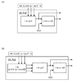
図1(A)に、本発明の一態様に係るPLDの構成例を、模式的に示す。図1(A)に示すPLD100は、複数のPLE(プログラマブルロジックエレメント)101を有するロジックアレイ102と、複数の記憶素子103を有するメモリエレメント104とを有する。メモリエレメント104は、ロジックアレイ102が形成されている層の上に設けられている。
本実施の形態では、メモリエレメント104の構成例について説明する。
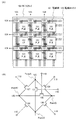
本実施の形態では、PLE101が有するLUT113の構成例について説明する。LUT113は複数のマルチプレクサを用いて構成することができる。そして、複数のマルチプレクサの入力端子及び制御端子のうちのいずれかにコンフィギュレーションデータ105が入力される構成とすることができる。
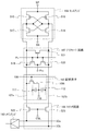
本実施の形態では、図6(A)に示した記憶素子103において、トランジスタ106tの活性層に酸化物半導体を用い、プログラマブルロジックエレメントが有するトランジスタ230の活性層にシリコンを用いる場合を例に挙げて、PLD及び半導体装置の作製方法について説明する。
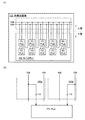
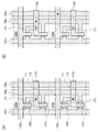
本実施の形態では、記憶素子103のレイアウトの一例と、記憶素子103が配線にそれぞれ置き換えられたレイアウトの一例とについて、説明する。
本発明の一態様に係る半導体装置またはプログラマブルロジックデバイスは、表示機器、パーソナルコンピュータ、記録媒体を備えた画像再生装置(代表的にはDVD:Digital Versatile Disc等の記録媒体を再生し、その画像を表示しうるディスプレイを有する装置)に用いることができる。その他に、本発明の一態様に係る半導体装置またはプログラマブルロジックデバイスを用いることができる電子機器として、携帯電話、携帯型を含むゲーム機、携帯情報端末、電子書籍、ビデオカメラ、デジタルスチルカメラなどのカメラ、ゴーグル型ディスプレイ(ヘッドマウントディスプレイ)、ナビゲーションシステム、音響再生装置(カーオーディオ、デジタルオーディオプレイヤー等)、複写機、ファクシミリ、プリンター、プリンター複合機、現金自動預け入れ払い機(ATM)、自動販売機などが挙げられる。これら電子機器の具体例を図16に示す。
32 マルチプレクサ
33 マルチプレクサ
34 マルチプレクサ
35 マルチプレクサ
36 マルチプレクサ
37 マルチプレクサ
41 マルチプレクサ
42 マルチプレクサ
43 マルチプレクサ
44 OR回路
100 PLD
101 PLE
102 ロジックアレイ
103 記憶素子
103a 記憶素子
103b 記憶素子
104 メモリエレメント
105 コンフィギュレーションデータ
106 スイッチ
106t トランジスタ
107 配線
107a 配線
107b 配線
107c 導電膜
108 配線
108c 導電膜
109 配線
109c 導電膜
110 ノード
110c 導電膜
111 容量素子
112 容量素子
113 LUT
114 レジスタ
115 コンフィギュレーションメモリ
120 半導体装置
121 配線群
122 スイッチ
123 配線エレメント
124 出力端子
125 配線
126 配線
127 トランジスタ
128 トランジスタ
129 トランジスタ
130 トランジスタ
131 トランジスタ
132 トランジスタ
140 I/Oエレメント
141 PLL
142 RAM
143 乗算器
150 配線
150c 導電膜
151t トランジスタ
160 セルアレイ
161 駆動回路
162 入出力バッファ
163 メインアンプ
164 カラムデコーダ
165 ローデコーダ
166 スイッチ回路
167 プリチャージ回路
168 センスアンプ
169 回路
170 導電膜
171 導電膜
230 トランジスタ
515 トランジスタ
516 トランジスタ
517 トランジスタ
518 トランジスタ
519 トランジスタ
520 トランジスタ
521 トランジスタ
522 トランジスタ
523 トランジスタ
700 基板
701 絶縁膜
702 半導体膜
703 ゲート絶縁膜
704 ゲート電極
705 チャネル形成領域
706 不純物領域
707 絶縁膜
708 絶縁膜
709 絶縁膜
710 導電膜
711 導電膜
712 導電膜
713 絶縁膜
714 絶縁膜
715 酸化物半導体膜
717 導電膜
718 導電膜
719 ゲート絶縁膜
720 ゲート電極
721 導電膜
722 絶縁膜
725 開口部
726 配線
727 絶縁膜
800 配線
5001 筐体
5002 筐体
5003 表示部
5004 表示部
5005 マイクロホン
5006 スピーカー
5007 操作キー
5008 スタイラス
5101 車体
5102 車輪
5103 ダッシュボード
5104 ライト
5301 筐体
5302 冷蔵室用扉
5303 冷凍室用扉
5401 筐体
5402 表示部
5403 キーボード
5404 ポインティングデバイス
5601 筐体
5602 筐体
5603 表示部
5604 表示部
5605 接続部
5606 操作キー
5801 筐体
5802 筐体
5803 表示部
5804 操作キー
5805 レンズ
5806 接続部
Claims (8)
- プログラマブルロジックエレメントと、
記憶素子と、を有し、
前記記憶素子は、第1のスイッチを有し、
前記記憶素子は、前記第1のスイッチを介して書き込まれるコンフィギュレーションデータを記憶する機能を有し、
前記プログラマブルロジックエレメントと前記記憶素子とに電気的に接続されたノードに、前記コンフィギュレーションデータに応じた電荷が与えられ、
前記ノードは、複数の配線のそれぞれと絶縁膜を介して重なる領域を有し、
前記絶縁膜は、酸化珪素又は酸化窒化珪素を含む半導体装置。 - 複数のプログラマブルロジックエレメントと、
配線エレメントと、
記憶素子と、を有し、
前記記憶素子は、第1のスイッチを有し、
前記記憶素子は、前記第1のスイッチを介して書き込まれるコンフィギュレーションデータを記憶する機能を有し、
前記プログラマブルロジックエレメントと前記記憶素子とに電気的に接続されたノードに、前記コンフィギュレーションデータに応じた電荷が与えられ、
前記ノードは、複数の配線のそれぞれと絶縁膜を介して重なる領域を有し、
前記絶縁膜は、酸化珪素又は酸化窒化珪素を含み、
前記複数のプログラマブルロジックエレメントは、前記コンフィギュレーションデータに従って定義された論理演算を行う機能を有し、
前記配線エレメントは、前記コンフィギュレーションデータに従って前記複数のプログラマブルロジックエレメント間の電気的な接続状態を制御する機能を有する半導体装置。 - プログラマブルロジックエレメントと、
記憶素子と、を有し、
前記記憶素子は、第1のスイッチと、第2のスイッチと、を有し、
前記記憶素子は、前記第1のスイッチを介して書き込まれるコンフィギュレーションデータを記憶する機能を有し、
前記第2のスイッチは、前記記憶素子において記憶される前記コンフィギュレーションデータを読み出す機能を有し、
前記プログラマブルロジックエレメントと前記記憶素子とに電気的に接続されたノードに、前記コンフィギュレーションデータに応じた電荷が与えられ、
前記ノードは、複数の配線のそれぞれと絶縁膜を介して重なる領域を有し、
前記絶縁膜は、酸化珪素又は酸化窒化珪素を含む半導体装置。 - 複数のプログラマブルロジックエレメントと、
配線エレメントと、
記憶素子と、を有し、
前記記憶素子は、第1のスイッチと、第2のスイッチと、を有し、
前記記憶素子は、前記第1のスイッチを介して書き込まれるコンフィギュレーションデータを記憶する機能を有し、
前記第2のスイッチは、前記記憶素子において記憶される前記コンフィギュレーションデータを読み出す機能を有し、
前記プログラマブルロジックエレメントと前記記憶素子とに電気的に接続されたノードに、前記コンフィギュレーションデータに応じた電荷が与えられ、
前記ノードは、複数の配線のそれぞれと絶縁膜を介して重なる領域を有し、
前記絶縁膜は、酸化珪素又は酸化窒化珪素を含み、
前記複数のプログラマブルロジックエレメントは、前記コンフィギュレーションデータに従って定義された論理演算を行う機能を有し、
前記配線エレメントは、前記コンフィギュレーションデータに従って前記複数のプログラマブルロジックエレメント間の電気的な接続状態を制御する機能を有する半導体装置。 - 請求項1乃至請求項4のいずれか一において、
前記第1のスイッチは、チャネル形成領域に酸化物半導体を含むトランジスタを有する半導体装置。 - 請求項5において、
前記プログラマブルロジックエレメントが有するトランジスタの上層に、前記第1のスイッチが有するトランジスタが位置する半導体装置。 - 請求項5又は請求項6において、
前記トランジスタのゲート絶縁膜は、化学量論的組成よりも多い酸素を含む領域を有する半導体装置。 - 請求項5乃至請求項7のいずれか一において、
前記トランジスタは、前記トランジスタのゲート絶縁膜から前記チャネル形成領域に酸素が供給される工程を経て形成される半導体装置の作製方法。
Priority Applications (1)
| Application Number | Priority Date | Filing Date | Title |
|---|---|---|---|
| JP2013012907A JP6125850B2 (ja) | 2012-02-09 | 2013-01-28 | 半導体装置及び半導体装置の作製方法 |
Applications Claiming Priority (3)
| Application Number | Priority Date | Filing Date | Title |
|---|---|---|---|
| JP2012026105 | 2012-02-09 | ||
| JP2012026105 | 2012-02-09 | ||
| JP2013012907A JP6125850B2 (ja) | 2012-02-09 | 2013-01-28 | 半導体装置及び半導体装置の作製方法 |
Related Child Applications (1)
| Application Number | Title | Priority Date | Filing Date |
|---|---|---|---|
| JP2017075811A Division JP6310116B2 (ja) | 2012-02-09 | 2017-04-06 | 半導体装置 |
Publications (3)
| Publication Number | Publication Date |
|---|---|
| JP2013179579A JP2013179579A (ja) | 2013-09-09 |
| JP2013179579A5 JP2013179579A5 (ja) | 2016-03-03 |
| JP6125850B2 true JP6125850B2 (ja) | 2017-05-10 |
Family
ID=48944901
Family Applications (4)
| Application Number | Title | Priority Date | Filing Date |
|---|---|---|---|
| JP2013012907A Expired - Fee Related JP6125850B2 (ja) | 2012-02-09 | 2013-01-28 | 半導体装置及び半導体装置の作製方法 |
| JP2017075811A Expired - Fee Related JP6310116B2 (ja) | 2012-02-09 | 2017-04-06 | 半導体装置 |
| JP2018047445A Expired - Fee Related JP6488037B2 (ja) | 2012-02-09 | 2018-03-15 | 半導体装置 |
| JP2019029941A Expired - Fee Related JP6708767B2 (ja) | 2012-02-09 | 2019-02-22 | 半導体装置 |
Family Applications After (3)
| Application Number | Title | Priority Date | Filing Date |
|---|---|---|---|
| JP2017075811A Expired - Fee Related JP6310116B2 (ja) | 2012-02-09 | 2017-04-06 | 半導体装置 |
| JP2018047445A Expired - Fee Related JP6488037B2 (ja) | 2012-02-09 | 2018-03-15 | 半導体装置 |
| JP2019029941A Expired - Fee Related JP6708767B2 (ja) | 2012-02-09 | 2019-02-22 | 半導体装置 |
Country Status (2)
| Country | Link |
|---|---|
| US (2) | US9379113B2 (ja) |
| JP (4) | JP6125850B2 (ja) |
Families Citing this family (46)
| Publication number | Priority date | Publication date | Assignee | Title |
|---|---|---|---|---|
| US9654107B2 (en) | 2012-04-27 | 2017-05-16 | Semiconductor Energy Laboratory Co., Ltd. | Programmable LSI |
| KR101978932B1 (ko) | 2012-05-02 | 2019-05-16 | 가부시키가이샤 한도오따이 에네루기 켄큐쇼 | 프로그램 가능한 로직 디바이스 |
| JP6250955B2 (ja) | 2012-05-25 | 2017-12-20 | 株式会社半導体エネルギー研究所 | 半導体装置の駆動方法 |
| CN104321967B (zh) | 2012-05-25 | 2018-01-09 | 株式会社半导体能源研究所 | 可编程逻辑装置及半导体装置 |
| JP6377317B2 (ja) | 2012-05-30 | 2018-08-22 | 株式会社半導体エネルギー研究所 | プログラマブルロジックデバイス |
| KR102102589B1 (ko) | 2012-10-17 | 2020-04-22 | 가부시키가이샤 한도오따이 에네루기 켄큐쇼 | 프로그램 가능한 논리 장치 |
| TWI591966B (zh) | 2012-10-17 | 2017-07-11 | 半導體能源研究所股份有限公司 | 可編程邏輯裝置及可編程邏輯裝置的驅動方法 |
| KR102112364B1 (ko) | 2012-12-06 | 2020-05-18 | 가부시키가이샤 한도오따이 에네루기 켄큐쇼 | 반도체 장치 |
| WO2014125979A1 (en) | 2013-02-13 | 2014-08-21 | Semiconductor Energy Laboratory Co., Ltd. | Programmable logic device and semiconductor device |
| US8952723B2 (en) | 2013-02-13 | 2015-02-10 | Semiconductor Energy Laboratory Co., Ltd. | Programmable logic device and semiconductor device |
| US8947121B2 (en) | 2013-03-12 | 2015-02-03 | Semiconductor Energy Laboratory Co., Ltd. | Programmable logic device |
| TWI621337B (zh) | 2013-05-14 | 2018-04-11 | 半導體能源研究所股份有限公司 | 信號處理裝置 |
| US9172369B2 (en) | 2013-05-17 | 2015-10-27 | Semiconductor Energy Laboratory Co., Ltd. | Programmable logic device and semiconductor device |
| JP6368155B2 (ja) | 2013-06-18 | 2018-08-01 | 株式会社半導体エネルギー研究所 | プログラマブルロジックデバイス |
| JP6483402B2 (ja) | 2013-11-01 | 2019-03-13 | 株式会社半導体エネルギー研究所 | 記憶装置、及び記憶装置を有する電子機器 |
| JP6478562B2 (ja) | 2013-11-07 | 2019-03-06 | 株式会社半導体エネルギー研究所 | 半導体装置 |
| JP6393590B2 (ja) * | 2013-11-22 | 2018-09-19 | 株式会社半導体エネルギー研究所 | 半導体装置 |
| JP6444723B2 (ja) | 2014-01-09 | 2018-12-26 | 株式会社半導体エネルギー研究所 | 装置 |
| US9379713B2 (en) | 2014-01-17 | 2016-06-28 | Semiconductor Energy Laboratory Co., Ltd. | Data processing device and driving method thereof |
| JP6521643B2 (ja) | 2014-01-24 | 2019-05-29 | 株式会社半導体エネルギー研究所 | 半導体装置 |
| US9721968B2 (en) | 2014-02-06 | 2017-08-01 | Semiconductor Energy Laboratory Co., Ltd. | Semiconductor device, electronic component, and electronic appliance |
| US9869716B2 (en) | 2014-02-07 | 2018-01-16 | Semiconductor Energy Laboratory Co., Ltd. | Device comprising programmable logic element |
| JP2015165226A (ja) | 2014-02-07 | 2015-09-17 | 株式会社半導体エネルギー研究所 | 装置 |
| JP6625328B2 (ja) | 2014-03-06 | 2019-12-25 | 株式会社半導体エネルギー研究所 | 半導体装置の駆動方法 |
| KR102267237B1 (ko) * | 2014-03-07 | 2021-06-18 | 가부시키가이샤 한도오따이 에네루기 켄큐쇼 | 반도체 장치 및 전자 기기 |
| JP6442321B2 (ja) | 2014-03-07 | 2018-12-19 | 株式会社半導体エネルギー研究所 | 半導体装置及びその駆動方法、並びに電子機器 |
| JP6541376B2 (ja) | 2014-03-13 | 2019-07-10 | 株式会社半導体エネルギー研究所 | プログラマブルロジックデバイスの動作方法 |
| TWI643457B (zh) | 2014-04-25 | 2018-12-01 | 日商半導體能源研究所股份有限公司 | 半導體裝置 |
| US9401364B2 (en) | 2014-09-19 | 2016-07-26 | Semiconductor Energy Laboratory Co., Ltd. | Semiconductor device, electronic component, and electronic device |
| US9836218B2 (en) * | 2014-10-03 | 2017-12-05 | Micron Technology, Inc. | Computing reduction and prefix sum operations in memory |
| JP6784259B2 (ja) * | 2015-09-02 | 2020-11-11 | 日本電気株式会社 | プログラマブル論理集積回路と半導体装置およびキャラクタライズ方法 |
| KR102643895B1 (ko) | 2015-10-30 | 2024-03-05 | 가부시키가이샤 한도오따이 에네루기 켄큐쇼 | 반도체 장치, 전자 부품, 및 전자 기기 |
| US10001963B2 (en) | 2015-12-01 | 2018-06-19 | Alson Technology Limited | Dynamic random access memory |
| JP6517720B2 (ja) * | 2016-03-16 | 2019-05-22 | 東芝メモリ株式会社 | 半導体記憶装置 |
| US9998119B2 (en) | 2016-05-20 | 2018-06-12 | Semiconductor Energy Laboratory Co., Ltd. | Semiconductor device, electronic component, and electronic device |
| DE112017004148T5 (de) | 2016-08-19 | 2019-05-23 | Semiconductor Energy Laboratory Co., Ltd. | Verfahren zum Steuern der Stromzufuhr in einer Halbleitervorrichtung |
| US10354716B2 (en) | 2016-09-16 | 2019-07-16 | Aspiring Sky Co. Limited | SRAM based memory structures and methods thereof |
| US11361813B2 (en) | 2016-09-16 | 2022-06-14 | Aspiring Sky Co. Limited | Nonvolatile memory structures with DRAM |
| US10353715B2 (en) | 2016-10-20 | 2019-07-16 | Aspiring Sky Co. Limited | Low power non-volatile SRAM memory systems |
| US10402342B2 (en) * | 2016-10-20 | 2019-09-03 | Aspiring Sky Co., Limited | Re-configurable non-volatile memory structures and systems |
| US10320390B1 (en) | 2016-11-17 | 2019-06-11 | X Development Llc | Field programmable gate array including coupled lookup tables |
| WO2018173812A1 (ja) * | 2017-03-22 | 2018-09-27 | 国立研究開発法人日本原子力研究開発機構 | イオンビーム機能性透過膜、イオンビーム機能性透過膜を用いたビームライン機器、イオンビーム機能性透過膜を用いたフィルター機器、フィルター機器の調整方法 |
| US10924112B2 (en) * | 2019-04-11 | 2021-02-16 | Ememory Technology Inc. | Bandgap reference circuit |
| JP7272587B2 (ja) * | 2019-10-04 | 2023-05-12 | 本田技研工業株式会社 | 半導体装置 |
| CN113901749B (zh) * | 2021-10-11 | 2022-09-30 | 江苏汤谷智能科技有限公司 | 一种fpga阵列结构及基于分部空间分段可编程时钟布线方法 |
| WO2025120505A1 (en) * | 2023-12-05 | 2025-06-12 | Zinite Corporation | Multi-planar static random-access memory |
Family Cites Families (128)
| Publication number | Priority date | Publication date | Assignee | Title |
|---|---|---|---|---|
| JPS60198861A (ja) | 1984-03-23 | 1985-10-08 | Fujitsu Ltd | 薄膜トランジスタ |
| JPH0244256B2 (ja) | 1987-01-28 | 1990-10-03 | Kagaku Gijutsucho Mukizaishitsu Kenkyushocho | Ingazn2o5deshimesarerurotsuhoshokeinosojokozoojusurukagobutsuoyobisonoseizoho |
| JPS63210023A (ja) | 1987-02-24 | 1988-08-31 | Natl Inst For Res In Inorg Mater | InGaZn↓4O↓7で示される六方晶系の層状構造を有する化合物およびその製造法 |
| JPH0244258B2 (ja) | 1987-02-24 | 1990-10-03 | Kagaku Gijutsucho Mukizaishitsu Kenkyushocho | Ingazn3o6deshimesarerurotsuhoshokeinosojokozoojusurukagobutsuoyobisonoseizoho |
| JPH0244260B2 (ja) | 1987-02-24 | 1990-10-03 | Kagaku Gijutsucho Mukizaishitsu Kenkyushocho | Ingazn5o8deshimesarerurotsuhoshokeinosojokozoojusurukagobutsuoyobisonoseizoho |
| JPH0244262B2 (ja) | 1987-02-27 | 1990-10-03 | Kagaku Gijutsucho Mukizaishitsu Kenkyushocho | Ingazn6o9deshimesarerurotsuhoshokeinosojokozoojusurukagobutsuoyobisonoseizoho |
| JPH0244263B2 (ja) | 1987-04-22 | 1990-10-03 | Kagaku Gijutsucho Mukizaishitsu Kenkyushocho | Ingazn7o10deshimesarerurotsuhoshokeinosojokozoojusurukagobutsuoyobisonoseizoho |
| JPH01130390A (ja) * | 1987-11-17 | 1989-05-23 | Hitachi Ltd | 配線スイッチ回路 |
| JPH02291720A (ja) | 1989-05-01 | 1990-12-03 | Kawasaki Steel Corp | プログラム可能な論理デバイス |
| JPH07111826B2 (ja) * | 1990-09-12 | 1995-11-29 | 株式会社東芝 | 半導体記憶装置 |
| JPH0553689A (ja) | 1991-08-23 | 1993-03-05 | Kawasaki Steel Corp | プログラマブル論理回路装置 |
| JPH05251705A (ja) | 1992-03-04 | 1993-09-28 | Fuji Xerox Co Ltd | 薄膜トランジスタ |
| JPH07202017A (ja) * | 1993-12-28 | 1995-08-04 | Hitachi Ltd | 半導体集積回路装置及びその製造方法 |
| JP3479375B2 (ja) | 1995-03-27 | 2003-12-15 | 科学技術振興事業団 | 亜酸化銅等の金属酸化物半導体による薄膜トランジスタとpn接合を形成した金属酸化物半導体装置およびそれらの製造方法 |
| JPH11505377A (ja) | 1995-08-03 | 1999-05-18 | フィリップス エレクトロニクス ネムローゼ フェンノートシャップ | 半導体装置 |
| JP3625598B2 (ja) | 1995-12-30 | 2005-03-02 | 三星電子株式会社 | 液晶表示装置の製造方法 |
| WO1998009327A1 (fr) | 1996-08-28 | 1998-03-05 | Hitachi, Ltd. | Procede de production d'un circuit integre a semiconducteur, et circuit integre a semiconducteur |
| JP4103968B2 (ja) | 1996-09-18 | 2008-06-18 | 株式会社半導体エネルギー研究所 | 絶縁ゲイト型半導体装置 |
| JP4170454B2 (ja) | 1998-07-24 | 2008-10-22 | Hoya株式会社 | 透明導電性酸化物薄膜を有する物品及びその製造方法 |
| JP2000150861A (ja) | 1998-11-16 | 2000-05-30 | Tdk Corp | 酸化物薄膜 |
| JP3276930B2 (ja) | 1998-11-17 | 2002-04-22 | 科学技術振興事業団 | トランジスタ及び半導体装置 |
| JP3447627B2 (ja) | 1999-09-02 | 2003-09-16 | 株式会社東芝 | スイッチング素子及び半導体集積回路 |
| TW460731B (en) | 1999-09-03 | 2001-10-21 | Ind Tech Res Inst | Electrode structure and production method of wide viewing angle LCD |
| KR100516693B1 (ko) | 2003-04-02 | 2005-09-22 | 주식회사 하이닉스반도체 | 불휘발성 프로그래머블 로직 회로 |
| KR100317331B1 (ko) | 1999-11-11 | 2001-12-24 | 박종섭 | 불휘발성 강유전체 메모리 소자 및 그 제조방법 |
| JP4089858B2 (ja) | 2000-09-01 | 2008-05-28 | 国立大学法人東北大学 | 半導体デバイス |
| KR20020038482A (ko) | 2000-11-15 | 2002-05-23 | 모리시타 요이찌 | 박막 트랜지스터 어레이, 그 제조방법 및 그것을 이용한표시패널 |
| JP3997731B2 (ja) | 2001-03-19 | 2007-10-24 | 富士ゼロックス株式会社 | 基材上に結晶性半導体薄膜を形成する方法 |
| JP2002289859A (ja) | 2001-03-23 | 2002-10-04 | Minolta Co Ltd | 薄膜トランジスタ |
| JP3925839B2 (ja) | 2001-09-10 | 2007-06-06 | シャープ株式会社 | 半導体記憶装置およびその試験方法 |
| JP4090716B2 (ja) | 2001-09-10 | 2008-05-28 | 雅司 川崎 | 薄膜トランジスタおよびマトリクス表示装置 |
| JP4164562B2 (ja) | 2002-09-11 | 2008-10-15 | 独立行政法人科学技術振興機構 | ホモロガス薄膜を活性層として用いる透明薄膜電界効果型トランジスタ |
| EP1443130B1 (en) | 2001-11-05 | 2011-09-28 | Japan Science and Technology Agency | Natural superlattice homologous single crystal thin film, method for preparation thereof, and device using said single crystal thin film |
| JP4083486B2 (ja) | 2002-02-21 | 2008-04-30 | 独立行政法人科学技術振興機構 | LnCuO(S,Se,Te)単結晶薄膜の製造方法 |
| US7049190B2 (en) | 2002-03-15 | 2006-05-23 | Sanyo Electric Co., Ltd. | Method for forming ZnO film, method for forming ZnO semiconductor layer, method for fabricating semiconductor device, and semiconductor device |
| JP3933591B2 (ja) | 2002-03-26 | 2007-06-20 | 淳二 城戸 | 有機エレクトロルミネッセント素子 |
| US7339187B2 (en) | 2002-05-21 | 2008-03-04 | State Of Oregon Acting By And Through The Oregon State Board Of Higher Education On Behalf Of Oregon State University | Transistor structures |
| JP2004022625A (ja) | 2002-06-13 | 2004-01-22 | Murata Mfg Co Ltd | 半導体デバイス及び該半導体デバイスの製造方法 |
| US7105868B2 (en) | 2002-06-24 | 2006-09-12 | Cermet, Inc. | High-electron mobility transistor with zinc oxide |
| US20040004239A1 (en) | 2002-07-08 | 2004-01-08 | Madurawe Raminda U. | Three dimensional integrated circuits |
| US7067843B2 (en) | 2002-10-11 | 2006-06-27 | E. I. Du Pont De Nemours And Company | Transparent oxide semiconductor thin film transistors |
| JP4166105B2 (ja) | 2003-03-06 | 2008-10-15 | シャープ株式会社 | 半導体装置およびその製造方法 |
| JP2004273732A (ja) | 2003-03-07 | 2004-09-30 | Sharp Corp | アクティブマトリクス基板およびその製造方法 |
| JP4108633B2 (ja) | 2003-06-20 | 2008-06-25 | シャープ株式会社 | 薄膜トランジスタおよびその製造方法ならびに電子デバイス |
| US7262463B2 (en) | 2003-07-25 | 2007-08-28 | Hewlett-Packard Development Company, L.P. | Transistor including a deposited channel region having a doped portion |
| US7064973B2 (en) | 2004-02-03 | 2006-06-20 | Klp International, Ltd. | Combination field programmable gate array allowing dynamic reprogrammability |
| US6972986B2 (en) | 2004-02-03 | 2005-12-06 | Kilopass Technologies, Inc. | Combination field programmable gate array allowing dynamic reprogrammability and non-votatile programmability based upon transistor gate oxide breakdown |
| US7145174B2 (en) | 2004-03-12 | 2006-12-05 | Hewlett-Packard Development Company, Lp. | Semiconductor device |
| US7297977B2 (en) | 2004-03-12 | 2007-11-20 | Hewlett-Packard Development Company, L.P. | Semiconductor device |
| EP1737044B1 (en) | 2004-03-12 | 2014-12-10 | Japan Science and Technology Agency | Amorphous oxide and thin film transistor |
| US7282782B2 (en) | 2004-03-12 | 2007-10-16 | Hewlett-Packard Development Company, L.P. | Combined binary oxide semiconductor device |
| US7211825B2 (en) | 2004-06-14 | 2007-05-01 | Yi-Chi Shih | Indium oxide-based thin film transistors and circuits |
| ITMI20041675A1 (it) * | 2004-08-30 | 2004-11-30 | St Microelectronics Srl | Blocco di commutazione e relativa matrice di commutazione, in particolare per architetture fpga. |
| JP2006100760A (ja) | 2004-09-02 | 2006-04-13 | Casio Comput Co Ltd | 薄膜トランジスタおよびその製造方法 |
| US7285501B2 (en) | 2004-09-17 | 2007-10-23 | Hewlett-Packard Development Company, L.P. | Method of forming a solution processed device |
| US7129749B1 (en) | 2004-10-27 | 2006-10-31 | Lattice Semiconductor Corporation | Programmable logic device having a configurable DRAM with transparent refresh |
| US7298084B2 (en) | 2004-11-02 | 2007-11-20 | 3M Innovative Properties Company | Methods and displays utilizing integrated zinc oxide row and column drivers in conjunction with organic light emitting diodes |
| US7791072B2 (en) | 2004-11-10 | 2010-09-07 | Canon Kabushiki Kaisha | Display |
| EP1815530B1 (en) | 2004-11-10 | 2021-02-17 | Canon Kabushiki Kaisha | Field effect transistor employing an amorphous oxide |
| US7453065B2 (en) | 2004-11-10 | 2008-11-18 | Canon Kabushiki Kaisha | Sensor and image pickup device |
| US7829444B2 (en) | 2004-11-10 | 2010-11-09 | Canon Kabushiki Kaisha | Field effect transistor manufacturing method |
| US7863611B2 (en) | 2004-11-10 | 2011-01-04 | Canon Kabushiki Kaisha | Integrated circuits utilizing amorphous oxides |
| KR100998527B1 (ko) | 2004-11-10 | 2010-12-07 | 고쿠리츠다이가쿠호진 토쿄고교 다이가꾸 | 비정질 산화물 및 전계 효과 트랜지스터 |
| RU2358354C2 (ru) | 2004-11-10 | 2009-06-10 | Кэнон Кабусики Кайся | Светоизлучающее устройство |
| US7579224B2 (en) | 2005-01-21 | 2009-08-25 | Semiconductor Energy Laboratory Co., Ltd. | Method for manufacturing a thin film semiconductor device |
| TWI505473B (zh) | 2005-01-28 | 2015-10-21 | 半導體能源研究所股份有限公司 | 半導體裝置,電子裝置,和半導體裝置的製造方法 |
| TWI481024B (zh) | 2005-01-28 | 2015-04-11 | 半導體能源研究所股份有限公司 | 半導體裝置,電子裝置,和半導體裝置的製造方法 |
| US7858451B2 (en) | 2005-02-03 | 2010-12-28 | Semiconductor Energy Laboratory Co., Ltd. | Electronic device, semiconductor device and manufacturing method thereof |
| US7948171B2 (en) | 2005-02-18 | 2011-05-24 | Semiconductor Energy Laboratory Co., Ltd. | Light emitting device |
| US20060197092A1 (en) | 2005-03-03 | 2006-09-07 | Randy Hoffman | System and method for forming conductive material on a substrate |
| US8681077B2 (en) | 2005-03-18 | 2014-03-25 | Semiconductor Energy Laboratory Co., Ltd. | Semiconductor device, and display device, driving method and electronic apparatus thereof |
| US7544967B2 (en) | 2005-03-28 | 2009-06-09 | Massachusetts Institute Of Technology | Low voltage flexible organic/transparent transistor for selective gas sensing, photodetecting and CMOS device applications |
| US7645478B2 (en) | 2005-03-31 | 2010-01-12 | 3M Innovative Properties Company | Methods of making displays |
| US8300031B2 (en) | 2005-04-20 | 2012-10-30 | Semiconductor Energy Laboratory Co., Ltd. | Semiconductor device comprising transistor having gate and drain connected through a current-voltage conversion element |
| JP2006313999A (ja) * | 2005-05-09 | 2006-11-16 | Renesas Technology Corp | 半導体装置 |
| JP2006344849A (ja) | 2005-06-10 | 2006-12-21 | Casio Comput Co Ltd | 薄膜トランジスタ |
| US7691666B2 (en) | 2005-06-16 | 2010-04-06 | Eastman Kodak Company | Methods of making thin film transistors comprising zinc-oxide-based semiconductor materials and transistors made thereby |
| US7402506B2 (en) | 2005-06-16 | 2008-07-22 | Eastman Kodak Company | Methods of making thin film transistors comprising zinc-oxide-based semiconductor materials and transistors made thereby |
| US7507618B2 (en) | 2005-06-27 | 2009-03-24 | 3M Innovative Properties Company | Method for making electronic devices using metal oxide nanoparticles |
| KR100711890B1 (ko) | 2005-07-28 | 2007-04-25 | 삼성에스디아이 주식회사 | 유기 발광표시장치 및 그의 제조방법 |
| JP2007059128A (ja) | 2005-08-23 | 2007-03-08 | Canon Inc | 有機el表示装置およびその製造方法 |
| JP4280736B2 (ja) | 2005-09-06 | 2009-06-17 | キヤノン株式会社 | 半導体素子 |
| JP2007073705A (ja) | 2005-09-06 | 2007-03-22 | Canon Inc | 酸化物半導体チャネル薄膜トランジスタおよびその製造方法 |
| JP5116225B2 (ja) | 2005-09-06 | 2013-01-09 | キヤノン株式会社 | 酸化物半導体デバイスの製造方法 |
| JP4850457B2 (ja) | 2005-09-06 | 2012-01-11 | キヤノン株式会社 | 薄膜トランジスタ及び薄膜ダイオード |
| EP1998373A3 (en) | 2005-09-29 | 2012-10-31 | Semiconductor Energy Laboratory Co, Ltd. | Semiconductor device having oxide semiconductor layer and manufacturing method thereof |
| JP5037808B2 (ja) | 2005-10-20 | 2012-10-03 | キヤノン株式会社 | アモルファス酸化物を用いた電界効果型トランジスタ、及び該トランジスタを用いた表示装置 |
| US7498835B1 (en) * | 2005-11-04 | 2009-03-03 | Xilinx, Inc. | Implementation of low power standby modes for integrated circuits |
| CN101577231B (zh) | 2005-11-15 | 2013-01-02 | 株式会社半导体能源研究所 | 半导体器件及其制造方法 |
| TWI292281B (en) | 2005-12-29 | 2008-01-01 | Ind Tech Res Inst | Pixel structure of active organic light emitting diode and method of fabricating the same |
| US7867636B2 (en) | 2006-01-11 | 2011-01-11 | Murata Manufacturing Co., Ltd. | Transparent conductive film and method for manufacturing the same |
| JP4977478B2 (ja) | 2006-01-21 | 2012-07-18 | 三星電子株式会社 | ZnOフィルム及びこれを用いたTFTの製造方法 |
| US7576394B2 (en) | 2006-02-02 | 2009-08-18 | Kochi Industrial Promotion Center | Thin film transistor including low resistance conductive thin films and manufacturing method thereof |
| US7977169B2 (en) | 2006-02-15 | 2011-07-12 | Kochi Industrial Promotion Center | Semiconductor device including active layer made of zinc oxide with controlled orientations and manufacturing method thereof |
| KR20070101595A (ko) | 2006-04-11 | 2007-10-17 | 삼성전자주식회사 | ZnO TFT |
| US20070252928A1 (en) | 2006-04-28 | 2007-11-01 | Toppan Printing Co., Ltd. | Structure, transmission type liquid crystal display, reflection type display and manufacturing method thereof |
| JP5028033B2 (ja) | 2006-06-13 | 2012-09-19 | キヤノン株式会社 | 酸化物半導体膜のドライエッチング方法 |
| JP4999400B2 (ja) | 2006-08-09 | 2012-08-15 | キヤノン株式会社 | 酸化物半導体膜のドライエッチング方法 |
| JP4609797B2 (ja) | 2006-08-09 | 2011-01-12 | Nec液晶テクノロジー株式会社 | 薄膜デバイス及びその製造方法 |
| JP4332545B2 (ja) | 2006-09-15 | 2009-09-16 | キヤノン株式会社 | 電界効果型トランジスタ及びその製造方法 |
| JP4274219B2 (ja) | 2006-09-27 | 2009-06-03 | セイコーエプソン株式会社 | 電子デバイス、有機エレクトロルミネッセンス装置、有機薄膜半導体装置 |
| JP5164357B2 (ja) | 2006-09-27 | 2013-03-21 | キヤノン株式会社 | 半導体装置及び半導体装置の製造方法 |
| US7622371B2 (en) | 2006-10-10 | 2009-11-24 | Hewlett-Packard Development Company, L.P. | Fused nanocrystal thin film semiconductor and method |
| US7772021B2 (en) | 2006-11-29 | 2010-08-10 | Samsung Electronics Co., Ltd. | Flat panel displays comprising a thin-film transistor having a semiconductive oxide in its channel and methods of fabricating the same for use in flat panel displays |
| JP2008140684A (ja) | 2006-12-04 | 2008-06-19 | Toppan Printing Co Ltd | カラーelディスプレイおよびその製造方法 |
| KR101303578B1 (ko) | 2007-01-05 | 2013-09-09 | 삼성전자주식회사 | 박막 식각 방법 |
| US8207063B2 (en) | 2007-01-26 | 2012-06-26 | Eastman Kodak Company | Process for atomic layer deposition |
| KR100851215B1 (ko) | 2007-03-14 | 2008-08-07 | 삼성에스디아이 주식회사 | 박막 트랜지스터 및 이를 이용한 유기 전계 발광표시장치 |
| US7795613B2 (en) | 2007-04-17 | 2010-09-14 | Toppan Printing Co., Ltd. | Structure with transistor |
| KR101325053B1 (ko) | 2007-04-18 | 2013-11-05 | 삼성디스플레이 주식회사 | 박막 트랜지스터 기판 및 이의 제조 방법 |
| KR20080094300A (ko) | 2007-04-19 | 2008-10-23 | 삼성전자주식회사 | 박막 트랜지스터 및 그 제조 방법과 박막 트랜지스터를포함하는 평판 디스플레이 |
| KR101334181B1 (ko) | 2007-04-20 | 2013-11-28 | 삼성전자주식회사 | 선택적으로 결정화된 채널층을 갖는 박막 트랜지스터 및 그제조 방법 |
| WO2008133345A1 (en) | 2007-04-25 | 2008-11-06 | Canon Kabushiki Kaisha | Oxynitride semiconductor |
| KR101345376B1 (ko) | 2007-05-29 | 2013-12-24 | 삼성전자주식회사 | ZnO 계 박막 트랜지스터 및 그 제조방법 |
| US8202365B2 (en) | 2007-12-17 | 2012-06-19 | Fujifilm Corporation | Process for producing oriented inorganic crystalline film, and semiconductor device using the oriented inorganic crystalline film |
| JP4623179B2 (ja) | 2008-09-18 | 2011-02-02 | ソニー株式会社 | 薄膜トランジスタおよびその製造方法 |
| JP5451280B2 (ja) | 2008-10-09 | 2014-03-26 | キヤノン株式会社 | ウルツ鉱型結晶成長用基板およびその製造方法ならびに半導体装置 |
| JP5781720B2 (ja) | 2008-12-15 | 2015-09-24 | ルネサスエレクトロニクス株式会社 | 半導体装置及び半導体装置の製造方法 |
| JP5476742B2 (ja) | 2009-02-27 | 2014-04-23 | 日本電気株式会社 | スイッチング素子、スイッチング素子の製造方法、電子デバイス、論理集積回路及びメモリ素子 |
| JP5415547B2 (ja) | 2009-09-25 | 2014-02-12 | 株式会社東芝 | メモリ機能付きパストランジスタ回路およびこのパストランジスタ回路を有するスイッチングボックス回路 |
| US8148728B2 (en) * | 2009-10-12 | 2012-04-03 | Monolithic 3D, Inc. | Method for fabrication of a semiconductor device and structure |
| KR101591613B1 (ko) * | 2009-10-21 | 2016-02-03 | 가부시키가이샤 한도오따이 에네루기 켄큐쇼 | 반도체 장치 |
| CN106057819B (zh) * | 2009-10-30 | 2019-03-15 | 株式会社半导体能源研究所 | 半导体装置 |
| WO2011052488A1 (en) | 2009-10-30 | 2011-05-05 | Semiconductor Energy Laboratory Co., Ltd. | Semiconductor device |
| CN105590646B (zh) * | 2009-12-25 | 2019-01-08 | 株式会社半导体能源研究所 | 存储器装置、半导体器件和电子装置 |
| KR101760537B1 (ko) * | 2009-12-28 | 2017-07-21 | 가부시키가이샤 한도오따이 에네루기 켄큐쇼 | 반도체 장치 |
| MY187143A (en) | 2010-01-20 | 2021-09-03 | Semiconductor Energy Lab | Semiconductor device |
| KR101899880B1 (ko) | 2011-02-17 | 2018-09-18 | 가부시키가이샤 한도오따이 에네루기 켄큐쇼 | 프로그래머블 lsi |
-
2013
- 2013-01-28 JP JP2013012907A patent/JP6125850B2/ja not_active Expired - Fee Related
- 2013-01-31 US US13/754,979 patent/US9379113B2/en not_active Expired - Fee Related
-
2016
- 2016-05-23 US US15/161,326 patent/US10600792B2/en not_active Expired - Fee Related
-
2017
- 2017-04-06 JP JP2017075811A patent/JP6310116B2/ja not_active Expired - Fee Related
-
2018
- 2018-03-15 JP JP2018047445A patent/JP6488037B2/ja not_active Expired - Fee Related
-
2019
- 2019-02-22 JP JP2019029941A patent/JP6708767B2/ja not_active Expired - Fee Related
Also Published As
| Publication number | Publication date |
|---|---|
| JP2013179579A (ja) | 2013-09-09 |
| JP2019125792A (ja) | 2019-07-25 |
| US20160268265A1 (en) | 2016-09-15 |
| US10600792B2 (en) | 2020-03-24 |
| US20130207170A1 (en) | 2013-08-15 |
| JP2017195368A (ja) | 2017-10-26 |
| JP6708767B2 (ja) | 2020-06-10 |
| JP2018137452A (ja) | 2018-08-30 |
| JP6488037B2 (ja) | 2019-03-20 |
| JP6310116B2 (ja) | 2018-04-11 |
| US9379113B2 (en) | 2016-06-28 |
Similar Documents
| Publication | Publication Date | Title |
|---|---|---|
| JP6488037B2 (ja) | 半導体装置 | |
| JP6144098B2 (ja) | プログラマブルlsi | |
| JP5886492B2 (ja) | プログラマブルlsi | |
| JP7038238B2 (ja) | 半導体装置 | |
| JP2021073738A (ja) | 半導体装置 | |
| JP5859839B2 (ja) | 記憶素子の駆動方法、及び、記憶素子 | |
| JP2022153594A (ja) | 半導体装置 | |
| JP2021170653A (ja) | 半導体装置 | |
| JP5731283B2 (ja) | 半導体装置 | |
| JP6145140B2 (ja) | 信号処理回路の作製方法 | |
| JP6028117B2 (ja) | 記憶装置 |
Legal Events
| Date | Code | Title | Description |
|---|---|---|---|
| A521 | Request for written amendment filed |
Free format text: JAPANESE INTERMEDIATE CODE: A523 Effective date: 20160111 |
|
| A621 | Written request for application examination |
Free format text: JAPANESE INTERMEDIATE CODE: A621 Effective date: 20160111 |
|
| A977 | Report on retrieval |
Free format text: JAPANESE INTERMEDIATE CODE: A971007 Effective date: 20160829 |
|
| A131 | Notification of reasons for refusal |
Free format text: JAPANESE INTERMEDIATE CODE: A131 Effective date: 20160913 |
|
| A521 | Request for written amendment filed |
Free format text: JAPANESE INTERMEDIATE CODE: A523 Effective date: 20161010 |
|
| TRDD | Decision of grant or rejection written | ||
| A01 | Written decision to grant a patent or to grant a registration (utility model) |
Free format text: JAPANESE INTERMEDIATE CODE: A01 Effective date: 20170321 |
|
| A61 | First payment of annual fees (during grant procedure) |
Free format text: JAPANESE INTERMEDIATE CODE: A61 Effective date: 20170406 |
|
| R150 | Certificate of patent or registration of utility model |
Ref document number: 6125850 Country of ref document: JP Free format text: JAPANESE INTERMEDIATE CODE: R150 |
|
| R250 | Receipt of annual fees |
Free format text: JAPANESE INTERMEDIATE CODE: R250 |
|
| R250 | Receipt of annual fees |
Free format text: JAPANESE INTERMEDIATE CODE: R250 |
|
| R250 | Receipt of annual fees |
Free format text: JAPANESE INTERMEDIATE CODE: R250 |
|
| LAPS | Cancellation because of no payment of annual fees |