JP5886584B2 - 半導体発光装置 - Google Patents
半導体発光装置 Download PDFInfo
- Publication number
- JP5886584B2 JP5886584B2 JP2011215534A JP2011215534A JP5886584B2 JP 5886584 B2 JP5886584 B2 JP 5886584B2 JP 2011215534 A JP2011215534 A JP 2011215534A JP 2011215534 A JP2011215534 A JP 2011215534A JP 5886584 B2 JP5886584 B2 JP 5886584B2
- Authority
- JP
- Japan
- Prior art keywords
- cathode
- anode
- emitting device
- semiconductor light
- light emitting
- Prior art date
- Legal status (The legal status is an assumption and is not a legal conclusion. Google has not performed a legal analysis and makes no representation as to the accuracy of the status listed.)
- Active
Links
- 239000004065 semiconductor Substances 0.000 title claims description 168
- 239000010410 layer Substances 0.000 claims description 107
- 239000000463 material Substances 0.000 claims description 92
- 239000000758 substrate Substances 0.000 claims description 79
- 229920005989 resin Polymers 0.000 claims description 72
- 239000011347 resin Substances 0.000 claims description 72
- 239000002344 surface layer Substances 0.000 claims description 70
- 238000007747 plating Methods 0.000 claims description 39
- 239000004020 conductor Substances 0.000 claims description 21
- 238000007789 sealing Methods 0.000 claims description 18
- 229910052737 gold Inorganic materials 0.000 claims description 16
- 229910045601 alloy Inorganic materials 0.000 claims description 13
- 239000000956 alloy Substances 0.000 claims description 13
- 239000000919 ceramic Substances 0.000 claims description 13
- 238000005304 joining Methods 0.000 claims description 13
- 229910052718 tin Inorganic materials 0.000 claims description 12
- 230000000149 penetrating effect Effects 0.000 claims description 7
- 230000017525 heat dissipation Effects 0.000 description 8
- 229910052751 metal Inorganic materials 0.000 description 8
- 239000002184 metal Substances 0.000 description 8
- 230000002441 reversible effect Effects 0.000 description 8
- 230000035515 penetration Effects 0.000 description 6
- 230000004308 accommodation Effects 0.000 description 5
- 238000004519 manufacturing process Methods 0.000 description 5
- 238000010304 firing Methods 0.000 description 4
- 239000011810 insulating material Substances 0.000 description 4
- 230000004048 modification Effects 0.000 description 4
- 238000012986 modification Methods 0.000 description 4
- 230000001737 promoting effect Effects 0.000 description 4
- 229910000679 solder Inorganic materials 0.000 description 4
- PNEYBMLMFCGWSK-UHFFFAOYSA-N aluminium oxide Inorganic materials [O-2].[O-2].[O-2].[Al+3].[Al+3] PNEYBMLMFCGWSK-UHFFFAOYSA-N 0.000 description 3
- 238000013016 damping Methods 0.000 description 3
- 230000036961 partial effect Effects 0.000 description 3
- 230000002829 reductive effect Effects 0.000 description 3
- 229920002050 silicone resin Polymers 0.000 description 3
- BQCADISMDOOEFD-UHFFFAOYSA-N Silver Chemical compound [Ag] BQCADISMDOOEFD-UHFFFAOYSA-N 0.000 description 2
- 230000000903 blocking effect Effects 0.000 description 2
- 229910010293 ceramic material Inorganic materials 0.000 description 2
- 239000003822 epoxy resin Substances 0.000 description 2
- 238000005530 etching Methods 0.000 description 2
- 238000000034 method Methods 0.000 description 2
- 229920000647 polyepoxide Polymers 0.000 description 2
- 229910052594 sapphire Inorganic materials 0.000 description 2
- 239000010980 sapphire Substances 0.000 description 2
- 229910052709 silver Inorganic materials 0.000 description 2
- 239000004332 silver Substances 0.000 description 2
- 230000003068 static effect Effects 0.000 description 2
- 229920005992 thermoplastic resin Polymers 0.000 description 2
- 229920001187 thermosetting polymer Polymers 0.000 description 2
- 241001085205 Prenanthella exigua Species 0.000 description 1
- GWEVSGVZZGPLCZ-UHFFFAOYSA-N Titan oxide Chemical compound O=[Ti]=O GWEVSGVZZGPLCZ-UHFFFAOYSA-N 0.000 description 1
- 229910052802 copper Inorganic materials 0.000 description 1
- 229910052742 iron Inorganic materials 0.000 description 1
- 239000007788 liquid Substances 0.000 description 1
- 230000000717 retained effect Effects 0.000 description 1
- 239000000523 sample Substances 0.000 description 1
- 238000005549 size reduction Methods 0.000 description 1
- OGIDPMRJRNCKJF-UHFFFAOYSA-N titanium oxide Inorganic materials [Ti]=O OGIDPMRJRNCKJF-UHFFFAOYSA-N 0.000 description 1
Images


Classifications
-
- H—ELECTRICITY
- H01—ELECTRIC ELEMENTS
- H01L—SEMICONDUCTOR DEVICES NOT COVERED BY CLASS H10
- H01L25/00—Assemblies consisting of a plurality of individual semiconductor or other solid state devices ; Multistep manufacturing processes thereof
- H01L25/03—Assemblies consisting of a plurality of individual semiconductor or other solid state devices ; Multistep manufacturing processes thereof all the devices being of a type provided for in the same subgroup of groups H01L27/00 - H01L33/00, or in a single subclass of H10K, H10N, e.g. assemblies of rectifier diodes
- H01L25/04—Assemblies consisting of a plurality of individual semiconductor or other solid state devices ; Multistep manufacturing processes thereof all the devices being of a type provided for in the same subgroup of groups H01L27/00 - H01L33/00, or in a single subclass of H10K, H10N, e.g. assemblies of rectifier diodes the devices not having separate containers
- H01L25/075—Assemblies consisting of a plurality of individual semiconductor or other solid state devices ; Multistep manufacturing processes thereof all the devices being of a type provided for in the same subgroup of groups H01L27/00 - H01L33/00, or in a single subclass of H10K, H10N, e.g. assemblies of rectifier diodes the devices not having separate containers the devices being of a type provided for in group H01L33/00
- H01L25/0753—Assemblies consisting of a plurality of individual semiconductor or other solid state devices ; Multistep manufacturing processes thereof all the devices being of a type provided for in the same subgroup of groups H01L27/00 - H01L33/00, or in a single subclass of H10K, H10N, e.g. assemblies of rectifier diodes the devices not having separate containers the devices being of a type provided for in group H01L33/00 the devices being arranged next to each other
-
- H—ELECTRICITY
- H01—ELECTRIC ELEMENTS
- H01L—SEMICONDUCTOR DEVICES NOT COVERED BY CLASS H10
- H01L27/00—Devices consisting of a plurality of semiconductor or other solid-state components formed in or on a common substrate
- H01L27/15—Devices consisting of a plurality of semiconductor or other solid-state components formed in or on a common substrate including semiconductor components with at least one potential-jump barrier or surface barrier specially adapted for light emission
-
- H—ELECTRICITY
- H01—ELECTRIC ELEMENTS
- H01L—SEMICONDUCTOR DEVICES NOT COVERED BY CLASS H10
- H01L33/00—Semiconductor devices with at least one potential-jump barrier or surface barrier specially adapted for light emission; Processes or apparatus specially adapted for the manufacture or treatment thereof or of parts thereof; Details thereof
- H01L33/02—Semiconductor devices with at least one potential-jump barrier or surface barrier specially adapted for light emission; Processes or apparatus specially adapted for the manufacture or treatment thereof or of parts thereof; Details thereof characterised by the semiconductor bodies
- H01L33/08—Semiconductor devices with at least one potential-jump barrier or surface barrier specially adapted for light emission; Processes or apparatus specially adapted for the manufacture or treatment thereof or of parts thereof; Details thereof characterised by the semiconductor bodies with a plurality of light emitting regions, e.g. laterally discontinuous light emitting layer or photoluminescent region integrated within the semiconductor body
-
- H—ELECTRICITY
- H01—ELECTRIC ELEMENTS
- H01L—SEMICONDUCTOR DEVICES NOT COVERED BY CLASS H10
- H01L33/00—Semiconductor devices with at least one potential-jump barrier or surface barrier specially adapted for light emission; Processes or apparatus specially adapted for the manufacture or treatment thereof or of parts thereof; Details thereof
- H01L33/48—Semiconductor devices with at least one potential-jump barrier or surface barrier specially adapted for light emission; Processes or apparatus specially adapted for the manufacture or treatment thereof or of parts thereof; Details thereof characterised by the semiconductor body packages
- H01L33/483—Containers
- H01L33/486—Containers adapted for surface mounting
-
- H—ELECTRICITY
- H01—ELECTRIC ELEMENTS
- H01L—SEMICONDUCTOR DEVICES NOT COVERED BY CLASS H10
- H01L33/00—Semiconductor devices with at least one potential-jump barrier or surface barrier specially adapted for light emission; Processes or apparatus specially adapted for the manufacture or treatment thereof or of parts thereof; Details thereof
- H01L33/48—Semiconductor devices with at least one potential-jump barrier or surface barrier specially adapted for light emission; Processes or apparatus specially adapted for the manufacture or treatment thereof or of parts thereof; Details thereof characterised by the semiconductor body packages
- H01L33/50—Wavelength conversion elements
- H01L33/507—Wavelength conversion elements the elements being in intimate contact with parts other than the semiconductor body or integrated with parts other than the semiconductor body
-
- H—ELECTRICITY
- H01—ELECTRIC ELEMENTS
- H01L—SEMICONDUCTOR DEVICES NOT COVERED BY CLASS H10
- H01L33/00—Semiconductor devices with at least one potential-jump barrier or surface barrier specially adapted for light emission; Processes or apparatus specially adapted for the manufacture or treatment thereof or of parts thereof; Details thereof
- H01L33/48—Semiconductor devices with at least one potential-jump barrier or surface barrier specially adapted for light emission; Processes or apparatus specially adapted for the manufacture or treatment thereof or of parts thereof; Details thereof characterised by the semiconductor body packages
- H01L33/52—Encapsulations
- H01L33/56—Materials, e.g. epoxy or silicone resin
-
- H—ELECTRICITY
- H01—ELECTRIC ELEMENTS
- H01L—SEMICONDUCTOR DEVICES NOT COVERED BY CLASS H10
- H01L33/00—Semiconductor devices with at least one potential-jump barrier or surface barrier specially adapted for light emission; Processes or apparatus specially adapted for the manufacture or treatment thereof or of parts thereof; Details thereof
- H01L33/48—Semiconductor devices with at least one potential-jump barrier or surface barrier specially adapted for light emission; Processes or apparatus specially adapted for the manufacture or treatment thereof or of parts thereof; Details thereof characterised by the semiconductor body packages
- H01L33/58—Optical field-shaping elements
- H01L33/60—Reflective elements
-
- H—ELECTRICITY
- H01—ELECTRIC ELEMENTS
- H01L—SEMICONDUCTOR DEVICES NOT COVERED BY CLASS H10
- H01L33/00—Semiconductor devices with at least one potential-jump barrier or surface barrier specially adapted for light emission; Processes or apparatus specially adapted for the manufacture or treatment thereof or of parts thereof; Details thereof
- H01L33/48—Semiconductor devices with at least one potential-jump barrier or surface barrier specially adapted for light emission; Processes or apparatus specially adapted for the manufacture or treatment thereof or of parts thereof; Details thereof characterised by the semiconductor body packages
- H01L33/62—Arrangements for conducting electric current to or from the semiconductor body, e.g. lead-frames, wire-bonds or solder balls
-
- H—ELECTRICITY
- H01—ELECTRIC ELEMENTS
- H01L—SEMICONDUCTOR DEVICES NOT COVERED BY CLASS H10
- H01L33/00—Semiconductor devices with at least one potential-jump barrier or surface barrier specially adapted for light emission; Processes or apparatus specially adapted for the manufacture or treatment thereof or of parts thereof; Details thereof
- H01L33/48—Semiconductor devices with at least one potential-jump barrier or surface barrier specially adapted for light emission; Processes or apparatus specially adapted for the manufacture or treatment thereof or of parts thereof; Details thereof characterised by the semiconductor body packages
- H01L33/64—Heat extraction or cooling elements
- H01L33/647—Heat extraction or cooling elements the elements conducting electric current to or from the semiconductor body
-
- H—ELECTRICITY
- H01—ELECTRIC ELEMENTS
- H01L—SEMICONDUCTOR DEVICES NOT COVERED BY CLASS H10
- H01L2224/00—Indexing scheme for arrangements for connecting or disconnecting semiconductor or solid-state bodies and methods related thereto as covered by H01L24/00
- H01L2224/01—Means for bonding being attached to, or being formed on, the surface to be connected, e.g. chip-to-package, die-attach, "first-level" interconnects; Manufacturing methods related thereto
- H01L2224/42—Wire connectors; Manufacturing methods related thereto
- H01L2224/47—Structure, shape, material or disposition of the wire connectors after the connecting process
- H01L2224/48—Structure, shape, material or disposition of the wire connectors after the connecting process of an individual wire connector
- H01L2224/484—Connecting portions
- H01L2224/48463—Connecting portions the connecting portion on the bonding area of the semiconductor or solid-state body being a ball bond
- H01L2224/48465—Connecting portions the connecting portion on the bonding area of the semiconductor or solid-state body being a ball bond the other connecting portion not on the bonding area being a wedge bond, i.e. ball-to-wedge, regular stitch
-
- H—ELECTRICITY
- H01—ELECTRIC ELEMENTS
- H01L—SEMICONDUCTOR DEVICES NOT COVERED BY CLASS H10
- H01L25/00—Assemblies consisting of a plurality of individual semiconductor or other solid state devices ; Multistep manufacturing processes thereof
- H01L25/16—Assemblies consisting of a plurality of individual semiconductor or other solid state devices ; Multistep manufacturing processes thereof the devices being of types provided for in two or more different main groups of groups H01L27/00 - H01L33/00, or in a single subclass of H10K, H10N, e.g. forming hybrid circuits
- H01L25/167—Assemblies consisting of a plurality of individual semiconductor or other solid state devices ; Multistep manufacturing processes thereof the devices being of types provided for in two or more different main groups of groups H01L27/00 - H01L33/00, or in a single subclass of H10K, H10N, e.g. forming hybrid circuits comprising optoelectronic devices, e.g. LED, photodiodes
Description
本発明は、上記した事情のもとで考え出されたものであって、小型化と高輝度化とを図ることが可能な半導体発光装置を提供することをその課題とする。
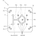
2 ケース
3 基材
31 表面
32 裏面
33 収容凹部
34 コーナー凹部
4 配線
41 表面層
41a アノードパッド
41b カソードパッド
41c バイパスカソードパッド
41d バイパスアノードパッド
41e アノードメッキ配線
41f カソードメッキ配線
41h 凹部(第2凹部)
42 中間層
42a カソード中継配線
43 裏面層
43a アノード実装電極
43b カソード実装電極
44 アノード貫通配線
44a 全厚アノード貫通配線
44b メッキ用アノード貫通配線
44c バイパスカソード貫通配線
44h 凹部(第1凹部)
45 カソード貫通配線
45a 表面側カソード貫通配線
45b 裏面側カソード貫通配線
45c メッキ用カソード貫通配線
45d バイパスアノード貫通配線
45h 凹部(第1凹部)
5 LEDチップ
5a 基板
5b n型半導体層
5c 活性層
5d p型半導体層
5e アノード電極
5f カソード電極
51 接合部
6 ツェナーダイオード
61 ワイヤ
8 充填部
7 封止樹脂
9 半導体発光装置
91 基材
92 リード
93 LEDチップ
94 半導体層
95 サブマウント基板
96 ワイヤ
97 封止樹脂
a,b 高さ
101,102,103,104,105 半導体発光装置
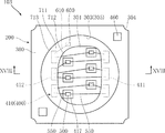
200 ケース
300 基材
301 表面
302 裏面
303 収容凹部
304 コーナー凹部
305 内壁面
306 せき止め凹部
307 包囲部
308 突出部
400 配線
410 表面層
411 アノードパッド
412 カソードパッド
413 バイパスカソードパッド
414 バイパスアノードパッド
417 ダイボンディングパッド
419 凹部(第2凹部)
420 中間層
421 カソード中継配線
430 裏面層
431 アノード実装電極
432 カソード実装電極
440 アノード貫通配線
441 全厚アノード貫通配線
443 バイパスカソード貫通配線
449 凹部(第1凹部)
450 カソード貫通配線
451 表面側カソード貫通配線
459 凹部(第1凹部)
460 テスト電極
461 アノード側面配線
462 カソード側面配線
500 LEDチップ
501 基板
502 n型半導体層
503 活性層
504 p型半導体層
505 アノード電極
506 カソード電極
507 サブマウント基板
510 接合部
511 導電性ペースト
550 ワイヤ
600 ツェナーダイオード(バイパス機能素子)
610 ワイヤ
700 封止樹脂
710 反射樹脂
711 反射面
712 内縁
713 外縁
800 充填部
Claims (32)
- 複数のLEDチップと、
上記複数のLEDチップが搭載されたケースと、を備え、
上記各LEDチップは、基板、およびこの基板に積層されたn型半導体層、活性層、p型半導体層、上記p型半導体層に導通するアノード電極および上記n型半導体層に導通するカソード電極を有しており、上記アノード電極および上記カソード電極が上記ケースと対面する姿勢で上記ケースに搭載されており、
上記ケースは、
セラミックからなり、かつ表面および裏面を有する基材と、
上記表面に形成された複数ずつのアノードパッドおよびカソードパッドを含む表面層、上記裏面に形成されたアノード実装電極およびカソード実装電極を含む裏面層、上記複数のアノードパッドと上記アノード実装電極とを導通させ、かつ上記基材の厚さ方向の少なくとも一部を貫通する複数のアノード貫通配線、上記複数のカソードパッドと上記カソード実装電極とを導通させ、かつ上記基材の厚さ方向の少なくとも一部を貫通する複数のカソード貫通配線、を有する配線と、
を有するとともに、
上記複数のアノード貫通配線および上記複数のカソード貫通配線の少なくともいずれかには、第1凹部が形成され、
上記表面層には、上記基材の厚さ方向視において、上記第1凹部に重なる第2凹部が形成され、
上記第2凹部に充填された充填部を更に備え、
上記充填部は、上記基材の厚さ方向視において上記複数のLEDチップのいずれか一つに重なることを特徴とする、半導体発光装置。 - 上記複数のアノード貫通配線は、上記表面から上記裏面まで上記基材を貫通する複数の全厚アノード貫通配線を含む、請求項1に記載の半導体発光装置。
- 上記配線は、上記基材の厚さ方向において上記表面および上記裏面の間に位置する中間層を有している、請求項1または請求項2に記載の半導体発光装置。
- 上記複数のカソード貫通配線は、上記表面から上記中間層まで上記基材を貫通している1以上の表面側カソード貫通配線と、上記中間層から上記裏面まで上記基材を貫通している1以上の裏面側カソード貫通配線と、を含む、請求項3に記載の半導体発光装置。
- 上記中間層は、上記表面側カソード貫通配線と、上記裏面側カソード貫通配線とにつながるカソード中継配線を有する、請求項4に記載の半導体発光装置。
- 上記表面層は、上記基材の厚さ方向視において上記基材の一端から上記基材の他端へと至るアノードメッキ配線およびカソードメッキ配線を有する、請求項1ないし請求項5のいずれかに記載の半導体発光装置。
- 上記複数のアノード貫通配線は、上記アノードメッキ配線と上記アノード実装電極とをつなぐメッキ用アノード貫通配線を含む、請求項6に記載の半導体発光装置。
- 上記複数のカソード貫通配線は、上記カソードメッキ配線と上記カソード実装電極とをつなぐメッキ用カソード貫通配線を含む、請求項6または請求項7に記載の半導体発光装置。
- 上記複数のアノード貫通配線のうち上記表面に露出するものは、その上記表面側端面が上記複数のアノードパッドによって覆われている、請求項1ないし請求項8のいずれかに記載の半導体発光装置。
- 上記複数のカソード貫通配線のうち上記表面に露出するものは、その上記表面側端面が上記複数のカソードパッドによって覆われている、請求項1ないし請求項9のいずれかに記載の半導体発光装置。
- 上記複数のアノード貫通配線のうち上記裏面に露出するものは、その上記裏面側端面が上記アノード実装電極によって覆われている、請求項1ないし請求項10のいずれかに記載の半導体発光装置。
- 上記複数のカソード貫通配線のうち上記裏面に露出するものは、その上記裏面側端面が上記カソード実装電極によって覆われている、請求項1ないし請求項11のいずれかに記載の半導体発光装置。
- 上記複数のアノード貫通配線および上記複数のカソード貫通配線は、Agからなる、請求項1ないし請求項12のいずれかに記載の半導体発光装置。
- 上記複数ずつのアノードパッドおよびカソードパッドは、Auからなる、請求項1ないし請求項13のいずれかに記載の半導体発光装置。
- 上記アノード実装電極および上記カソード実装電極は、Auからなる、請求項1ないし請求項14のいずれかに記載の半導体発光装置。
- 上記配線は、上記表面に形成されたバイパスカソードパッドおよびバイパスアノードパッドを有しており、
上記複数のアノード貫通配線は、上記バイパスカソードパッドと上記アノード実装電極とを導通させるバイパスカソード貫通配線を含んでおり、
上記複数のカソード貫通配線は、上記バイパスアノードパッドと上記カソード実装電極とを導通させるバイパスアノード貫通配線を含んでいる、請求項1ないし請求項15のいずれかに記載の半導体発光装置。 - 上記バイパスカソードパッドにはツェナーダイオードが導通接合されており、
上記バイパスアノードパッドと上記ツェナーダイオードとを導通させるワイヤを備える、請求項16に記載の半導体発光装置。 - 上記ケースには、その厚さ方向において上記複数のLEDチップを収容する収容凹部が形成されている、請求項1ないし請求項17のいずれかに記載の半導体発光装置。
- 上記収容凹部には、上記複数のLEDチップを覆う封止樹脂が充填されている、請求項18に記載の半導体発光装置。
- 上記封止樹脂は、上記LEDチップからの光によって励起されることにより上記LEDチップからの光とは異なる波長の光を発する蛍光材料が混入されている、請求項19に記載の半導体発光装置。
- 上記ケースは、その厚さ方向において略矩形状であり、その四隅には、厚さ方向断面形状が四半円状のコーナー凹部が形成されている、請求項1ないし請求項20のいずれかに記載の半導体発光装置。
- 上記複数のLEDチップのいずれか一つおよび上記表面層の間に介在する接合部を更に備え、
上記充填部は、上記接合部および上記表面層の間に介在し、且つ、上記接合部および上記表面層のいずれにも接している、請求項1ないし21のいずれかに記載の半導体発光装置。 - 上記充填部は、導電性の材料よりなる、請求項22に記載の半導体発光装置。
- 上記充填部は、AuとSnとの合金よりなる、請求項23に記載の半導体発光装置。
- 上記接合部は、導電性の材料よりなる、請求項22ないし請求項24のいずれかに記載の半導体発光装置。
- 上記接合部は、AuとSnとの合金よりなる、請求項25に記載の半導体発光装置。
- 1以上のLEDチップと、
上記LEDチップが搭載された表面、およびこの表面とは反対側に位置する裏面を有するケースとを備えた半導体発光装置であって、
上記ケースは、上記LEDチップを囲む内壁面を有する基材を含んでおり、
上記LEDチップ側に位置する内縁、上記内壁面に接する外縁、これら内縁および外縁を繋いでおり、かつ上記内縁から上記外縁に向かうほど上記表面から離間するように傾斜した反射面、を有する反射樹脂を備えるとともに、
上記ケースは、表面層、裏面層、複数のアノード貫通配線、および複数のカソード貫通配線を含み、
上記表面層は、上記基材の表面に形成された複数ずつのアノードパッドおよびカソードパッドを含み、
上記裏面層は、上記基材の裏面に形成されたアノード実装電極およびカソード実装電極を含み、
上記複数のアノード貫通配線は、上記複数のアノードパッドと上記アノード実装電極とを導通させ、かつ上記基材の厚さ方向の少なくとも一部を貫通しており、
上記複数のカソード貫通配線は、上記複数のカソードパッドと上記カソード実装電極とを導通させ、かつ上記基材の厚さ方向の少なくとも一部を貫通しており、
上記複数のアノード貫通配線および上記複数のカソード貫通配線の少なくともいずれかには、第1凹部が形成され、
上記表面層には、上記基材の厚さ方向視において、上記第1凹部に重なる第2凹部が形成され、
上記第2凹部に充填された充填部を更に備え、
上記充填部は、上記基材の厚さ方向視において上記複数のLEDチップのいずれか一つに重なることを特徴とする、半導体発光装置。 - 上記複数のLEDチップのいずれか一つおよび上記表面層の間に介在する接合部を更に備え、
上記充填部は、上記接合部および上記表面層の間に介在し、且つ、上記接合部および上記表面層のいずれにも接している、請求項27に記載の半導体発光装置。 - 上記充填部は、導電性の材料よりなる、請求項28に記載の半導体発光装置。
- 上記充填部は、AuとSnとの合金よりなる、請求項29に記載の半導体発光装置。
- 上記接合部は、導電性の材料よりなる、請求項28ないし請求項30のいずれかに記載の半導体発光装置。
- 上記接合部は、AuとSnとの合金よりなる、請求項31に記載の半導体発光装置。
Priority Applications (7)
| Application Number | Priority Date | Filing Date | Title |
|---|---|---|---|
| JP2011215534A JP5886584B2 (ja) | 2010-11-05 | 2011-09-29 | 半導体発光装置 |
| US13/289,288 US8648373B2 (en) | 2010-11-05 | 2011-11-04 | Semiconductor light emitting device |
| US14/105,437 US9035333B2 (en) | 2010-11-05 | 2013-12-13 | Semiconductor light emitting device |
| US14/695,915 US9276187B2 (en) | 2010-11-05 | 2015-04-24 | Semiconductor light emitting device |
| US15/018,435 US9496473B2 (en) | 2010-11-05 | 2016-02-08 | Semiconductor light emitting device |
| US15/288,337 US9728523B2 (en) | 2010-11-05 | 2016-10-07 | Semiconductor light emitting device |
| US15/642,501 US10056357B2 (en) | 2010-11-05 | 2017-07-06 | Semiconductor light emitting device |
Applications Claiming Priority (5)
| Application Number | Priority Date | Filing Date | Title |
|---|---|---|---|
| JP2010248494 | 2010-11-05 | ||
| JP2010248494 | 2010-11-05 | ||
| JP2010292644 | 2010-12-28 | ||
| JP2010292644 | 2010-12-28 | ||
| JP2011215534A JP5886584B2 (ja) | 2010-11-05 | 2011-09-29 | 半導体発光装置 |
Related Child Applications (1)
| Application Number | Title | Priority Date | Filing Date |
|---|---|---|---|
| JP2016024289A Division JP2016086191A (ja) | 2010-11-05 | 2016-02-12 | 半導体発光装置 |
Publications (2)
| Publication Number | Publication Date |
|---|---|
| JP2012151436A JP2012151436A (ja) | 2012-08-09 |
| JP5886584B2 true JP5886584B2 (ja) | 2016-03-16 |
Family
ID=46018770
Family Applications (1)
| Application Number | Title | Priority Date | Filing Date |
|---|---|---|---|
| JP2011215534A Active JP5886584B2 (ja) | 2010-11-05 | 2011-09-29 | 半導体発光装置 |
Country Status (2)
| Country | Link |
|---|---|
| US (6) | US8648373B2 (ja) |
| JP (1) | JP5886584B2 (ja) |
Families Citing this family (60)
| Publication number | Priority date | Publication date | Assignee | Title |
|---|---|---|---|---|
| JP2016086191A (ja) * | 2010-11-05 | 2016-05-19 | ローム株式会社 | 半導体発光装置 |
| JP6034175B2 (ja) * | 2012-01-10 | 2016-11-30 | ローム株式会社 | Ledモジュール |
| KR101997243B1 (ko) * | 2012-09-13 | 2019-07-08 | 엘지이노텍 주식회사 | 발광 소자 및 조명 시스템 |
| JP6147977B2 (ja) | 2012-09-26 | 2017-06-14 | ローム株式会社 | Led照明器具およびledユニット |
| JP6056336B2 (ja) * | 2012-09-28 | 2017-01-11 | 日亜化学工業株式会社 | 発光装置 |
| JP6102187B2 (ja) | 2012-10-31 | 2017-03-29 | 日亜化学工業株式会社 | 発光装置用パッケージ及びそれを用いた発光装置 |
| JP2014112669A (ja) * | 2012-11-12 | 2014-06-19 | Citizen Holdings Co Ltd | 半導体発光装置及びその製造方法 |
| JP6564159B2 (ja) * | 2012-12-07 | 2019-08-21 | 株式会社カネカ | 半導体発光装置 |
| JP6107136B2 (ja) | 2012-12-29 | 2017-04-05 | 日亜化学工業株式会社 | 発光装置用パッケージ及びそれを備える発光装置、並びにその発光装置を備える照明装置 |
| DE102013202904A1 (de) * | 2013-02-22 | 2014-08-28 | Osram Opto Semiconductors Gmbh | Optoelektronisches Halbleiterbauteil und Verfahren zu seiner Herstellung |
| CN104037053A (zh) * | 2013-03-04 | 2014-09-10 | 海洋王照明科技股份有限公司 | 场发射平面光源 |
| JP2014241341A (ja) * | 2013-06-11 | 2014-12-25 | 株式会社東芝 | 半導体発光装置 |
| WO2014203825A1 (ja) * | 2013-06-18 | 2014-12-24 | ローム株式会社 | Led光源モジュール |
| JP6192377B2 (ja) * | 2013-06-18 | 2017-09-06 | ローム株式会社 | Led光源モジュール |
| JP6221403B2 (ja) * | 2013-06-26 | 2017-11-01 | 日亜化学工業株式会社 | 発光装置 |
| JP6484396B2 (ja) | 2013-06-28 | 2019-03-13 | 日亜化学工業株式会社 | 発光装置用パッケージ及びそれを用いた発光装置 |
| US9887324B2 (en) | 2013-09-16 | 2018-02-06 | Lg Innotek Co., Ltd. | Light emitting device package |
| JP6331376B2 (ja) | 2013-12-17 | 2018-05-30 | 日亜化学工業株式会社 | 発光装置の製造方法及び発光装置 |
| KR102299238B1 (ko) * | 2014-01-08 | 2021-09-07 | 루미리즈 홀딩 비.브이. | 파장 변환 반도체 발광 디바이스 |
| CN103794701B (zh) * | 2014-01-26 | 2017-01-18 | 广东晶科电子股份有限公司 | 一种led支架及其led器件 |
| JP6213428B2 (ja) * | 2014-03-12 | 2017-10-18 | 豊田合成株式会社 | 発光装置及びその製造方法 |
| US9691949B2 (en) * | 2014-05-30 | 2017-06-27 | Cree, Inc. | Submount based light emitter components and methods |
| TWD167977S (zh) * | 2014-06-27 | 2015-05-21 | 隆達電子股份有限公司 | 發光二極體用導線架 |
| TWI556478B (zh) * | 2014-06-30 | 2016-11-01 | 億光電子工業股份有限公司 | 發光二極體裝置 |
| BR102015027316B1 (pt) | 2014-10-31 | 2021-07-27 | Nichia Corporation | Dispositivo emissor de luz e sistema de lâmpada frontal de farol de acionamento adaptativo |
| JP6547548B2 (ja) * | 2014-10-31 | 2019-07-24 | 日亜化学工業株式会社 | 発光装置及び配光可変ヘッドランプシステム |
| JP6762736B2 (ja) * | 2015-03-16 | 2020-09-30 | 晶元光電股▲ふん▼有限公司Epistar Corporation | 光反射層付光半導体素子、および、光反射層および蛍光体層付光半導体素子の製造方法 |
| JP6332636B2 (ja) * | 2015-03-26 | 2018-05-30 | 豊田合成株式会社 | 発光装置及び該発光装置用の封止層 |
| CN105006508B (zh) * | 2015-07-02 | 2017-07-25 | 厦门市三安光电科技有限公司 | 发光二极管封装结构 |
| JP6551009B2 (ja) * | 2015-07-27 | 2019-07-31 | ウシオ電機株式会社 | 光源装置 |
| JP6332342B2 (ja) * | 2015-08-20 | 2018-05-30 | 日亜化学工業株式会社 | 発光装置及び発光装置の製造方法 |
| US9502623B1 (en) * | 2015-10-02 | 2016-11-22 | Nichia Corporation | Light emitting device |
| US10008648B2 (en) * | 2015-10-08 | 2018-06-26 | Semicon Light Co., Ltd. | Semiconductor light emitting device |
| JP6862141B2 (ja) * | 2015-10-14 | 2021-04-21 | エルジー イノテック カンパニー リミテッド | 発光素子パッケージ及び照明装置 |
| KR102481646B1 (ko) * | 2015-11-12 | 2022-12-29 | 삼성전자주식회사 | 반도체 발광소자 패키지 |
| JP6278035B2 (ja) * | 2015-11-27 | 2018-02-14 | 日亜化学工業株式会社 | 発光装置の製造方法 |
| JP6572757B2 (ja) * | 2015-11-30 | 2019-09-11 | 日亜化学工業株式会社 | 発光装置 |
| JP6213582B2 (ja) * | 2016-01-22 | 2017-10-18 | 日亜化学工業株式会社 | 発光装置 |
| JP6493348B2 (ja) | 2016-09-30 | 2019-04-03 | 日亜化学工業株式会社 | 発光装置 |
| CN106356442A (zh) * | 2016-11-21 | 2017-01-25 | 莆田莆阳照明有限公司 | 一种led倒装晶片的全周光led灯 |
| CN106647031B (zh) * | 2016-12-27 | 2023-11-07 | 京东方科技集团股份有限公司 | 一种发光模块、显示装置及发光模块的制作方法 |
| WO2018168033A1 (ja) * | 2017-03-16 | 2018-09-20 | テイ・エス テック株式会社 | 照明装置 |
| CN110870064B (zh) * | 2017-07-07 | 2024-02-02 | 科锐Led公司 | 带有bsy发射器的rgb led封装件 |
| US10256218B2 (en) * | 2017-07-11 | 2019-04-09 | Samsung Electronics Co., Ltd. | Light emitting device package |
| US10680145B2 (en) * | 2017-08-04 | 2020-06-09 | Everlight Electronics Co., Ltd. | LED package structure and method for manufacturing same |
| JP6512316B2 (ja) * | 2018-01-19 | 2019-05-15 | 日亜化学工業株式会社 | 発光装置 |
| CN110197864B (zh) * | 2018-02-26 | 2022-06-14 | 世迈克琉明有限公司 | 半导体发光器件及其制造方法 |
| US10957736B2 (en) | 2018-03-12 | 2021-03-23 | Cree, Inc. | Light emitting diode (LED) components and methods |
| JP6680311B2 (ja) * | 2018-06-04 | 2020-04-15 | 日亜化学工業株式会社 | 発光装置および面発光光源 |
| JP7007589B2 (ja) * | 2018-07-24 | 2022-01-24 | 日亜化学工業株式会社 | 発光装置 |
| JP6669208B2 (ja) * | 2018-08-02 | 2020-03-18 | 日亜化学工業株式会社 | 発光装置 |
| US11189764B2 (en) * | 2018-11-22 | 2021-11-30 | Nichia Corporation | Light-emitting device and manufacturing method thereof |
| US20210074880A1 (en) * | 2018-12-18 | 2021-03-11 | Bolb Inc. | Light-output-power self-awareness light-emitting device |
| CN109741685B (zh) * | 2019-02-18 | 2021-11-02 | 深圳市洲明科技股份有限公司 | 一种led显示模组及其制作方法 |
| TWI688139B (zh) * | 2019-03-05 | 2020-03-11 | 友達光電股份有限公司 | 檢測裝置的製造方法與檢測方法 |
| JP6741102B2 (ja) * | 2019-03-06 | 2020-08-19 | 日亜化学工業株式会社 | 発光装置 |
| US10811578B1 (en) * | 2019-03-27 | 2020-10-20 | Lextar Electronics Corporation | LED carrier and LED package having the same |
| CN111987082B (zh) * | 2019-05-21 | 2022-07-26 | 光宝光电(常州)有限公司 | Led封装结构 |
| JP7353312B2 (ja) | 2021-01-07 | 2023-09-29 | シーシーエス株式会社 | Led光源、及び、led光源の検査方法 |
| CN113594334B (zh) * | 2021-07-15 | 2023-10-27 | 福建天电光电有限公司 | 新型半导体支架 |
Family Cites Families (19)
| Publication number | Priority date | Publication date | Assignee | Title |
|---|---|---|---|---|
| JPH11135838A (ja) * | 1997-10-20 | 1999-05-21 | Ind Technol Res Inst | 白色発光ダイオード及びその製造方法 |
| US6724798B2 (en) * | 2001-12-31 | 2004-04-20 | Honeywell International Inc. | Optoelectronic devices and method of production |
| DE10229067B4 (de) * | 2002-06-28 | 2007-08-16 | Osram Opto Semiconductors Gmbh | Optoelektronisches Bauelement und Verfahren zu dessen Herstellung |
| JP4201167B2 (ja) | 2002-09-26 | 2008-12-24 | シチズン電子株式会社 | 白色発光装置の製造方法 |
| WO2005073621A1 (ja) * | 2004-01-29 | 2005-08-11 | Matsushita Electric Industrial Co., Ltd. | Led照明光源 |
| JP4776175B2 (ja) | 2004-04-27 | 2011-09-21 | 京セラ株式会社 | 発光素子収納用パッケージおよびその製造方法および発光装置および照明装置 |
| JP2006156510A (ja) * | 2004-11-26 | 2006-06-15 | Ngk Spark Plug Co Ltd | 配線基板 |
| JP5008262B2 (ja) | 2005-03-02 | 2012-08-22 | 日亜化学工業株式会社 | 半導体発光素子 |
| JP2008060344A (ja) * | 2006-08-31 | 2008-03-13 | Toshiba Corp | 半導体発光装置 |
| JP2008270563A (ja) | 2007-04-20 | 2008-11-06 | Toyoda Gosei Co Ltd | 発光装置、光源装置及び発光装置の製造方法 |
| JP2008277349A (ja) * | 2007-04-25 | 2008-11-13 | Kyocera Corp | 発光素子搭載用基体、及びその製造方法、ならびに発光装置 |
| KR101365621B1 (ko) * | 2007-09-04 | 2014-02-24 | 서울반도체 주식회사 | 열 방출 슬러그들을 갖는 발광 다이오드 패키지 |
| JP2009295892A (ja) * | 2008-06-09 | 2009-12-17 | Nichia Corp | 発光装置 |
| JP2010118528A (ja) | 2008-11-13 | 2010-05-27 | Sumitomo Metal Electronics Devices Inc | リフレクタ及びこれを用いる発光素子搭載用パッケージ |
| JP5300439B2 (ja) | 2008-11-27 | 2013-09-25 | 京セラ株式会社 | 発光ランプ及び発光ランプを用いた照明装置 |
| JP2010199547A (ja) * | 2009-01-30 | 2010-09-09 | Nichia Corp | 発光装置及びその製造方法 |
| JP5539658B2 (ja) * | 2009-02-26 | 2014-07-02 | 日鉄住金エレクトロデバイス株式会社 | 反射材およびそれを用いた反射体および発光素子搭載用基板 |
| EP2448028B1 (en) * | 2010-10-29 | 2017-05-31 | Nichia Corporation | Light emitting apparatus and production method thereof |
| JPWO2012131792A1 (ja) * | 2011-03-31 | 2014-07-24 | パナソニック株式会社 | 半導体発光装置 |
-
2011
- 2011-09-29 JP JP2011215534A patent/JP5886584B2/ja active Active
- 2011-11-04 US US13/289,288 patent/US8648373B2/en active Active
-
2013
- 2013-12-13 US US14/105,437 patent/US9035333B2/en active Active
-
2015
- 2015-04-24 US US14/695,915 patent/US9276187B2/en active Active
-
2016
- 2016-02-08 US US15/018,435 patent/US9496473B2/en active Active
- 2016-10-07 US US15/288,337 patent/US9728523B2/en active Active
-
2017
- 2017-07-06 US US15/642,501 patent/US10056357B2/en active Active
Also Published As
| Publication number | Publication date |
|---|---|
| US9276187B2 (en) | 2016-03-01 |
| US20120112227A1 (en) | 2012-05-10 |
| US10056357B2 (en) | 2018-08-21 |
| US9728523B2 (en) | 2017-08-08 |
| US9035333B2 (en) | 2015-05-19 |
| US20150280094A1 (en) | 2015-10-01 |
| US20170309602A1 (en) | 2017-10-26 |
| US8648373B2 (en) | 2014-02-11 |
| US20160155918A1 (en) | 2016-06-02 |
| US20140103370A1 (en) | 2014-04-17 |
| JP2012151436A (ja) | 2012-08-09 |
| US9496473B2 (en) | 2016-11-15 |
| US20170025396A1 (en) | 2017-01-26 |
Similar Documents
| Publication | Publication Date | Title |
|---|---|---|
| JP5886584B2 (ja) | 半導体発光装置 | |
| US9735133B2 (en) | Light-emitting device and lighting device provided with the same | |
| TWI692122B (zh) | 發光二極體封裝結構及其製作方法 | |
| JP6131048B2 (ja) | Ledモジュール | |
| KR101360732B1 (ko) | 발광 다이오드 패키지 | |
| JP6892261B2 (ja) | Ledパッケージ | |
| TW200828635A (en) | Light emitting device, its manufacturing method and its mounted substrate | |
| JP5167977B2 (ja) | 半導体装置 | |
| JP7212753B2 (ja) | 半導体発光装置 | |
| JP2008078401A (ja) | 照明装置 | |
| JP2008251664A (ja) | 照明装置 | |
| JPWO2018105448A1 (ja) | 発光装置 | |
| JP6107229B2 (ja) | 発光装置 | |
| JP5401025B2 (ja) | 発光モジュールおよびその製造方法 | |
| JP2007280983A (ja) | 発光装置 | |
| JP5939977B2 (ja) | Ledモジュール | |
| JP2007027539A (ja) | 半導体発光素子およびこれを用いた照明装置 | |
| JP5055837B2 (ja) | 発光装置 | |
| JP2007335734A (ja) | 半導体装置 | |
| JP5030009B2 (ja) | 発光装置 | |
| KR20140042187A (ko) | 발광 장치 | |
| JP2019087570A (ja) | 発光装置およびledパッケージ | |
| JP7323836B2 (ja) | 光源装置 | |
| KR20170037907A (ko) | 발광 장치 | |
| JP2006173196A (ja) | 発光素子及びこれを用いた発光ダイオード |
Legal Events
| Date | Code | Title | Description |
|---|---|---|---|
| A621 | Written request for application examination |
Free format text: JAPANESE INTERMEDIATE CODE: A621 Effective date: 20140926 |
|
| A131 | Notification of reasons for refusal |
Free format text: JAPANESE INTERMEDIATE CODE: A131 Effective date: 20150630 |
|
| A977 | Report on retrieval |
Free format text: JAPANESE INTERMEDIATE CODE: A971007 Effective date: 20150630 |
|
| A521 | Request for written amendment filed |
Free format text: JAPANESE INTERMEDIATE CODE: A523 Effective date: 20150827 |
|
| TRDD | Decision of grant or rejection written | ||
| A01 | Written decision to grant a patent or to grant a registration (utility model) |
Free format text: JAPANESE INTERMEDIATE CODE: A01 Effective date: 20160112 |
|
| A61 | First payment of annual fees (during grant procedure) |
Free format text: JAPANESE INTERMEDIATE CODE: A61 Effective date: 20160212 |
|
| R150 | Certificate of patent or registration of utility model |
Ref document number: 5886584 Country of ref document: JP Free format text: JAPANESE INTERMEDIATE CODE: R150 |
|
| R250 | Receipt of annual fees |
Free format text: JAPANESE INTERMEDIATE CODE: R250 |
|
| R250 | Receipt of annual fees |
Free format text: JAPANESE INTERMEDIATE CODE: R250 |
|
| R250 | Receipt of annual fees |
Free format text: JAPANESE INTERMEDIATE CODE: R250 |
|
| R250 | Receipt of annual fees |
Free format text: JAPANESE INTERMEDIATE CODE: R250 |
|
| R250 | Receipt of annual fees |
Free format text: JAPANESE INTERMEDIATE CODE: R250 |