JP5886584B2 - Semiconductor light emitting device - Google Patents
Semiconductor light emitting device Download PDFInfo
- Publication number
- JP5886584B2 JP5886584B2 JP2011215534A JP2011215534A JP5886584B2 JP 5886584 B2 JP5886584 B2 JP 5886584B2 JP 2011215534 A JP2011215534 A JP 2011215534A JP 2011215534 A JP2011215534 A JP 2011215534A JP 5886584 B2 JP5886584 B2 JP 5886584B2
- Authority
- JP
- Japan
- Prior art keywords
- cathode
- anode
- emitting device
- semiconductor light
- light emitting
- Prior art date
- Legal status (The legal status is an assumption and is not a legal conclusion. Google has not performed a legal analysis and makes no representation as to the accuracy of the status listed.)
- Active
Links
- 239000004065 semiconductor Substances 0.000 title claims description 168
- 239000010410 layer Substances 0.000 claims description 107
- 239000000463 material Substances 0.000 claims description 92
- 239000000758 substrate Substances 0.000 claims description 79
- 229920005989 resin Polymers 0.000 claims description 72
- 239000011347 resin Substances 0.000 claims description 72
- 239000002344 surface layer Substances 0.000 claims description 70
- 238000007747 plating Methods 0.000 claims description 39
- 239000004020 conductor Substances 0.000 claims description 21
- 238000007789 sealing Methods 0.000 claims description 18
- 229910052737 gold Inorganic materials 0.000 claims description 16
- 229910045601 alloy Inorganic materials 0.000 claims description 13
- 239000000956 alloy Substances 0.000 claims description 13
- 239000000919 ceramic Substances 0.000 claims description 13
- 238000005304 joining Methods 0.000 claims description 13
- 229910052718 tin Inorganic materials 0.000 claims description 12
- 230000000149 penetrating effect Effects 0.000 claims description 7
- 230000017525 heat dissipation Effects 0.000 description 8
- 229910052751 metal Inorganic materials 0.000 description 8
- 239000002184 metal Substances 0.000 description 8
- 230000002441 reversible effect Effects 0.000 description 8
- 230000035515 penetration Effects 0.000 description 6
- 230000004308 accommodation Effects 0.000 description 5
- 238000004519 manufacturing process Methods 0.000 description 5
- 238000010304 firing Methods 0.000 description 4
- 239000011810 insulating material Substances 0.000 description 4
- 230000004048 modification Effects 0.000 description 4
- 238000012986 modification Methods 0.000 description 4
- 230000001737 promoting effect Effects 0.000 description 4
- 229910000679 solder Inorganic materials 0.000 description 4
- PNEYBMLMFCGWSK-UHFFFAOYSA-N aluminium oxide Inorganic materials [O-2].[O-2].[O-2].[Al+3].[Al+3] PNEYBMLMFCGWSK-UHFFFAOYSA-N 0.000 description 3
- 238000013016 damping Methods 0.000 description 3
- 230000036961 partial effect Effects 0.000 description 3
- 230000002829 reductive effect Effects 0.000 description 3
- 229920002050 silicone resin Polymers 0.000 description 3
- BQCADISMDOOEFD-UHFFFAOYSA-N Silver Chemical compound [Ag] BQCADISMDOOEFD-UHFFFAOYSA-N 0.000 description 2
- 230000000903 blocking effect Effects 0.000 description 2
- 229910010293 ceramic material Inorganic materials 0.000 description 2
- 239000003822 epoxy resin Substances 0.000 description 2
- 238000005530 etching Methods 0.000 description 2
- 238000000034 method Methods 0.000 description 2
- 229920000647 polyepoxide Polymers 0.000 description 2
- 229910052594 sapphire Inorganic materials 0.000 description 2
- 239000010980 sapphire Substances 0.000 description 2
- 229910052709 silver Inorganic materials 0.000 description 2
- 239000004332 silver Substances 0.000 description 2
- 230000003068 static effect Effects 0.000 description 2
- 229920005992 thermoplastic resin Polymers 0.000 description 2
- 229920001187 thermosetting polymer Polymers 0.000 description 2
- 241001085205 Prenanthella exigua Species 0.000 description 1
- GWEVSGVZZGPLCZ-UHFFFAOYSA-N Titan oxide Chemical compound O=[Ti]=O GWEVSGVZZGPLCZ-UHFFFAOYSA-N 0.000 description 1
- 229910052802 copper Inorganic materials 0.000 description 1
- 229910052742 iron Inorganic materials 0.000 description 1
- 239000007788 liquid Substances 0.000 description 1
- 230000000717 retained effect Effects 0.000 description 1
- 239000000523 sample Substances 0.000 description 1
- 238000005549 size reduction Methods 0.000 description 1
- OGIDPMRJRNCKJF-UHFFFAOYSA-N titanium oxide Inorganic materials [Ti]=O OGIDPMRJRNCKJF-UHFFFAOYSA-N 0.000 description 1
Images


Classifications
-
- H—ELECTRICITY
- H01—ELECTRIC ELEMENTS
- H01L—SEMICONDUCTOR DEVICES NOT COVERED BY CLASS H10
- H01L25/00—Assemblies consisting of a plurality of individual semiconductor or other solid state devices ; Multistep manufacturing processes thereof
- H01L25/03—Assemblies consisting of a plurality of individual semiconductor or other solid state devices ; Multistep manufacturing processes thereof all the devices being of a type provided for in the same subgroup of groups H01L27/00 - H01L33/00, or in a single subclass of H10K, H10N, e.g. assemblies of rectifier diodes
- H01L25/04—Assemblies consisting of a plurality of individual semiconductor or other solid state devices ; Multistep manufacturing processes thereof all the devices being of a type provided for in the same subgroup of groups H01L27/00 - H01L33/00, or in a single subclass of H10K, H10N, e.g. assemblies of rectifier diodes the devices not having separate containers
- H01L25/075—Assemblies consisting of a plurality of individual semiconductor or other solid state devices ; Multistep manufacturing processes thereof all the devices being of a type provided for in the same subgroup of groups H01L27/00 - H01L33/00, or in a single subclass of H10K, H10N, e.g. assemblies of rectifier diodes the devices not having separate containers the devices being of a type provided for in group H01L33/00
- H01L25/0753—Assemblies consisting of a plurality of individual semiconductor or other solid state devices ; Multistep manufacturing processes thereof all the devices being of a type provided for in the same subgroup of groups H01L27/00 - H01L33/00, or in a single subclass of H10K, H10N, e.g. assemblies of rectifier diodes the devices not having separate containers the devices being of a type provided for in group H01L33/00 the devices being arranged next to each other
-
- H—ELECTRICITY
- H01—ELECTRIC ELEMENTS
- H01L—SEMICONDUCTOR DEVICES NOT COVERED BY CLASS H10
- H01L27/00—Devices consisting of a plurality of semiconductor or other solid-state components formed in or on a common substrate
- H01L27/15—Devices consisting of a plurality of semiconductor or other solid-state components formed in or on a common substrate including semiconductor components having potential barriers, specially adapted for light emission
-
- H—ELECTRICITY
- H01—ELECTRIC ELEMENTS
- H01L—SEMICONDUCTOR DEVICES NOT COVERED BY CLASS H10
- H01L33/00—Semiconductor devices having potential barriers specially adapted for light emission; Processes or apparatus specially adapted for the manufacture or treatment thereof or of parts thereof; Details thereof
- H01L33/02—Semiconductor devices having potential barriers specially adapted for light emission; Processes or apparatus specially adapted for the manufacture or treatment thereof or of parts thereof; Details thereof characterised by the semiconductor bodies
- H01L33/08—Semiconductor devices having potential barriers specially adapted for light emission; Processes or apparatus specially adapted for the manufacture or treatment thereof or of parts thereof; Details thereof characterised by the semiconductor bodies with a plurality of light emitting regions, e.g. laterally discontinuous light emitting layer or photoluminescent region integrated within the semiconductor body
-
- H—ELECTRICITY
- H01—ELECTRIC ELEMENTS
- H01L—SEMICONDUCTOR DEVICES NOT COVERED BY CLASS H10
- H01L33/00—Semiconductor devices having potential barriers specially adapted for light emission; Processes or apparatus specially adapted for the manufacture or treatment thereof or of parts thereof; Details thereof
- H01L33/48—Semiconductor devices having potential barriers specially adapted for light emission; Processes or apparatus specially adapted for the manufacture or treatment thereof or of parts thereof; Details thereof characterised by the semiconductor body packages
- H01L33/483—Containers
- H01L33/486—Containers adapted for surface mounting
-
- H—ELECTRICITY
- H01—ELECTRIC ELEMENTS
- H01L—SEMICONDUCTOR DEVICES NOT COVERED BY CLASS H10
- H01L33/00—Semiconductor devices having potential barriers specially adapted for light emission; Processes or apparatus specially adapted for the manufacture or treatment thereof or of parts thereof; Details thereof
- H01L33/48—Semiconductor devices having potential barriers specially adapted for light emission; Processes or apparatus specially adapted for the manufacture or treatment thereof or of parts thereof; Details thereof characterised by the semiconductor body packages
- H01L33/50—Wavelength conversion elements
- H01L33/507—Wavelength conversion elements the elements being in intimate contact with parts other than the semiconductor body or integrated with parts other than the semiconductor body
-
- H—ELECTRICITY
- H01—ELECTRIC ELEMENTS
- H01L—SEMICONDUCTOR DEVICES NOT COVERED BY CLASS H10
- H01L33/00—Semiconductor devices having potential barriers specially adapted for light emission; Processes or apparatus specially adapted for the manufacture or treatment thereof or of parts thereof; Details thereof
- H01L33/48—Semiconductor devices having potential barriers specially adapted for light emission; Processes or apparatus specially adapted for the manufacture or treatment thereof or of parts thereof; Details thereof characterised by the semiconductor body packages
- H01L33/52—Encapsulations
- H01L33/56—Materials, e.g. epoxy or silicone resin
-
- H—ELECTRICITY
- H01—ELECTRIC ELEMENTS
- H01L—SEMICONDUCTOR DEVICES NOT COVERED BY CLASS H10
- H01L33/00—Semiconductor devices having potential barriers specially adapted for light emission; Processes or apparatus specially adapted for the manufacture or treatment thereof or of parts thereof; Details thereof
- H01L33/48—Semiconductor devices having potential barriers specially adapted for light emission; Processes or apparatus specially adapted for the manufacture or treatment thereof or of parts thereof; Details thereof characterised by the semiconductor body packages
- H01L33/58—Optical field-shaping elements
- H01L33/60—Reflective elements
-
- H—ELECTRICITY
- H01—ELECTRIC ELEMENTS
- H01L—SEMICONDUCTOR DEVICES NOT COVERED BY CLASS H10
- H01L33/00—Semiconductor devices having potential barriers specially adapted for light emission; Processes or apparatus specially adapted for the manufacture or treatment thereof or of parts thereof; Details thereof
- H01L33/48—Semiconductor devices having potential barriers specially adapted for light emission; Processes or apparatus specially adapted for the manufacture or treatment thereof or of parts thereof; Details thereof characterised by the semiconductor body packages
- H01L33/62—Arrangements for conducting electric current to or from the semiconductor body, e.g. lead-frames, wire-bonds or solder balls
-
- H—ELECTRICITY
- H01—ELECTRIC ELEMENTS
- H01L—SEMICONDUCTOR DEVICES NOT COVERED BY CLASS H10
- H01L33/00—Semiconductor devices having potential barriers specially adapted for light emission; Processes or apparatus specially adapted for the manufacture or treatment thereof or of parts thereof; Details thereof
- H01L33/48—Semiconductor devices having potential barriers specially adapted for light emission; Processes or apparatus specially adapted for the manufacture or treatment thereof or of parts thereof; Details thereof characterised by the semiconductor body packages
- H01L33/64—Heat extraction or cooling elements
- H01L33/647—Heat extraction or cooling elements the elements conducting electric current to or from the semiconductor body
-
- H—ELECTRICITY
- H01—ELECTRIC ELEMENTS
- H01L—SEMICONDUCTOR DEVICES NOT COVERED BY CLASS H10
- H01L2224/00—Indexing scheme for arrangements for connecting or disconnecting semiconductor or solid-state bodies and methods related thereto as covered by H01L24/00
- H01L2224/01—Means for bonding being attached to, or being formed on, the surface to be connected, e.g. chip-to-package, die-attach, "first-level" interconnects; Manufacturing methods related thereto
- H01L2224/42—Wire connectors; Manufacturing methods related thereto
- H01L2224/47—Structure, shape, material or disposition of the wire connectors after the connecting process
- H01L2224/48—Structure, shape, material or disposition of the wire connectors after the connecting process of an individual wire connector
- H01L2224/484—Connecting portions
- H01L2224/48463—Connecting portions the connecting portion on the bonding area of the semiconductor or solid-state body being a ball bond
- H01L2224/48465—Connecting portions the connecting portion on the bonding area of the semiconductor or solid-state body being a ball bond the other connecting portion not on the bonding area being a wedge bond, i.e. ball-to-wedge, regular stitch
-
- H—ELECTRICITY
- H01—ELECTRIC ELEMENTS
- H01L—SEMICONDUCTOR DEVICES NOT COVERED BY CLASS H10
- H01L25/00—Assemblies consisting of a plurality of individual semiconductor or other solid state devices ; Multistep manufacturing processes thereof
- H01L25/16—Assemblies consisting of a plurality of individual semiconductor or other solid state devices ; Multistep manufacturing processes thereof the devices being of types provided for in two or more different main groups of groups H01L27/00 - H01L33/00, or in a single subclass of H10K, H10N, e.g. forming hybrid circuits
- H01L25/167—Assemblies consisting of a plurality of individual semiconductor or other solid state devices ; Multistep manufacturing processes thereof the devices being of types provided for in two or more different main groups of groups H01L27/00 - H01L33/00, or in a single subclass of H10K, H10N, e.g. forming hybrid circuits comprising optoelectronic devices, e.g. LED, photodiodes
Landscapes
- Engineering & Computer Science (AREA)
- Microelectronics & Electronic Packaging (AREA)
- Power Engineering (AREA)
- Computer Hardware Design (AREA)
- Manufacturing & Machinery (AREA)
- Physics & Mathematics (AREA)
- Condensed Matter Physics & Semiconductors (AREA)
- General Physics & Mathematics (AREA)
- Led Device Packages (AREA)
Description
本発明は、半導体発光装置に関する。 The present invention relates to a semiconductor light emitting device.
図27は、従来の半導体発光装置の一例を示している。同図に示された半導体発光装置9は、基材91にリード92が設けられている。リード92には、LEDチップ93が実装されている。LEDチップ93は、半導体層94およびサブマウント基板95を有する。半導体層94は、たとえばn型半導体層、p型半導体層、およびこれらに挟まれた活性層を有する。サブマウント基板95は、半導体層94を支持しており、たとえばSiからなる。LEDチップ93は、ワイヤ96によってリード92に導通している。封止樹脂97は、LEDチップ93を覆っており、LEDチップ93からの光を透過する。
FIG. 27 shows an example of a conventional semiconductor light emitting device. In the semiconductor light emitting device 9 shown in the figure, a
LEDチップ93が発光すると、主に上記活性層から熱が発生する。この熱は、リード92および基材91へと伝えられることにより放熱される。しかしながら、上記活性層とリード92との間には、サブマウント基板95が介在している。このサブマウント基板95は、LEDチップ93からの放熱を妨げる。したがって、LEDチップ93の発光効率が低下するという問題があった。
When the
図28は、従来の半導体発光装置の他の一例を示している(たとえば、特許文献2参照)。同図に示された半導体発光装置900は、基板901にLEDチップ902が搭載されている。LEDチップ902は、枠状のリフレクタ905によって囲まれている。リフレクタ905によって囲まれた空間には、封止樹脂906が充填されている。LEDチップ902は、たとえばSiからなるサブマウント基板903とサブマウント基板903上に積層された半導体層904を有する。半導体層904は、サブマウント基板903を介して基板901に導通している。
FIG. 28 shows another example of a conventional semiconductor light emitting device (see, for example, Patent Document 2). In the semiconductor
LEDチップ902から側方に出射した光は、リフレクタ905によって上向きに反射される。反射された光をより多く半導体発光装置900から出射するには、リフレクタ905の内壁面を基板901に対して直角である角度から大きく傾けることが有効である。しかしながら、上記内壁面を傾けるほど、半導体発光装置900が大きくなってしまう。半導体発光装置900は、搭載される電子機器などのスペース制約から、小型化の要請が強い。このため、半導体発光装置900の小型化と高輝度化とを両立することは困難である。
Light emitted from the
本発明は、上記した事情のもとで考え出されたものであって、LEDチップからの放熱を促進し、発光効率を高めることが可能な半導体発光装置を提供することをその課題とする。
本発明は、上記した事情のもとで考え出されたものであって、小型化と高輝度化とを図ることが可能な半導体発光装置を提供することをその課題とする。
The present invention has been conceived under the circumstances described above, and it is an object of the present invention to provide a semiconductor light-emitting device capable of promoting heat dissipation from the LED chip and increasing the light emission efficiency.
The present invention has been conceived under the circumstances described above, and it is an object of the present invention to provide a semiconductor light emitting device that can be reduced in size and brightness.
本発明の第1の側面によると、複数のLEDチップと、上記複数のLEDチップが搭載されたケースと、を備え、上記各LEDチップは、基板、およびこの基板に積層されたn型半導体層、活性層、p型半導体層、上記p型半導体層に導通するアノード電極および上記n型半導体層に導通するカソード電極を有しており、上記アノード電極および上記カソード電極が上記ケースと対面する姿勢で上記ケースに搭載されており、上記ケースは、セラミックからなり、かつ表面および裏面を有する基材と、上記表面に形成された複数ずつのアノードパッドおよびカソードパッドを含む表面層、上記裏面に形成されたアノード実装電極およびカソード実装電極を含む裏面層、上記複数のアノードパッドと上記アノード実装電極とを導通させ、かつ上記基材の厚さ方向の少なくとも一部を貫通する複数のアノード貫通配線、上記複数のカソードパッドと上記カソード実装電極とを導通させ、かつ上記基材の厚さ方向の少なくとも一部を貫通する複数のカソード貫通配線、を有する配線と、を有することを特徴とする、半導体発光装置が提供される。 According to a first aspect of the present invention, a plurality of LED chips and a case on which the plurality of LED chips are mounted are provided. Each of the LED chips includes a substrate and an n-type semiconductor layer stacked on the substrate. An active layer, a p-type semiconductor layer, an anode electrode conducting to the p-type semiconductor layer, and a cathode electrode conducting to the n-type semiconductor layer, wherein the anode electrode and the cathode electrode face the case The case is made of ceramic and has a front surface and a back surface, a surface layer including a plurality of anode pads and cathode pads formed on the front surface, and formed on the back surface. A back surface layer including an anode mounting electrode and a cathode mounting electrode, electrically connecting the plurality of anode pads and the anode mounting electrode; and A plurality of anode through-wirings penetrating at least part of the thickness direction of the base material, a plurality of the cathode pads and the cathode mounting electrode are electrically connected, and a plurality of holes penetrating at least part of the base material in the thickness direction There is provided a semiconductor light emitting device comprising: a wiring having a cathode through wiring.
好ましくは、上記複数のアノード貫通配線は、上記表面から上記裏面まで上記基材を貫通する複数の全厚アノード貫通配線を含む。 Preferably, the plurality of anode through wirings include a plurality of full thickness anode through wirings that penetrate the base material from the front surface to the back surface.
好ましくは、上記配線は、上記基材の厚さ方向において上記表面および上記裏面の間に位置する中間層を有している。 Preferably, the wiring has an intermediate layer located between the front surface and the back surface in the thickness direction of the base material.
好ましくは、上記複数のカソード貫通配線は、上記表面から上記中間層まで上記基材を貫通している1以上の表面側カソード貫通配線と、上記中間層から上記裏面まで上記基材を貫通している1以上の裏面側カソード貫通配線と、を含む。 Preferably, the plurality of through-cathode wirings pass through the base material from one or more front side cathode through wirings penetrating the base material from the surface to the intermediate layer and from the intermediate layer to the back surface. One or more backside cathode through wirings.
好ましくは、上記中間層は、上記表面側カソード貫通配線と、上記裏面側カソード貫通配線とにつながるカソード中継配線を有する。 Preferably, the intermediate layer includes a cathode relay wiring connected to the front surface side cathode through wiring and the back surface side cathode through wiring.
好ましくは、上記表面層は、上記基材の厚さ方向視において上記基材の一端から上記基材の他端へと至るアノードメッキ配線およびカソードメッキ配線を有する。 Preferably, the surface layer has an anode plating wiring and a cathode plating wiring extending from one end of the base material to the other end of the base material as viewed in the thickness direction of the base material.
好ましくは、上記複数のアノード貫通配線は、上記アノードメッキ配線と上記アノード実装電極とをつなぐメッキ用アノード貫通配線を含む。 Preferably, the plurality of anode through wirings include a plating anode through wiring that connects the anode plating wiring and the anode mounting electrode.
好ましくは、上記複数のカソード貫通配線は、上記カソードメッキ配線と上記カソード実装電極とをつなぐメッキ用カソード貫通配線を含む。 Preferably, the plurality of cathode through wirings include a plating cathode through wiring that connects the cathode plating wiring and the cathode mounting electrode.
好ましくは、上記複数のアノード貫通配線のうち上記表面に露出するものは、その上記表面側端面が上記複数のアノードパッドによって覆われている。 Preferably, among the plurality of through-anode wirings, the surface-side end surface of the one exposed on the surface is covered with the plurality of anode pads.
好ましくは、上記複数のカソード貫通配線のうち上記表面に露出するものは、その上記表面側端面が上記複数のカソードパッドによって覆われている。 Preferably, among the plurality of through-cathode wirings, those exposed on the surface have the surface-side end surfaces covered with the plurality of cathode pads.
好ましくは、上記複数のアノード貫通配線のうち上記裏面に露出するものは、その上記裏面側端面が上記アノード実装電極によって覆われている。 Preferably, among the plurality of through-anode wirings, those exposed on the back surface have their back-side end surfaces covered with the anode mounting electrodes.
好ましくは、上記複数のカソード貫通配線のうち上記裏面に露出するものは、その上記裏面側端面が上記カソード実装電極によって覆われている。 Preferably, of the plurality of through-cathode wirings, those exposed on the back surface are covered with the cathode mounting electrode at the back surface side end surface.
好ましくは、上記複数のアノード貫通配線および上記複数のカソード貫通配線は、Agからなる。 Preferably, the plurality of anode through wires and the plurality of cathode through wires are made of Ag.
好ましくは、上記複数ずつのアノードパッドおよびカソードパッドは、Auからなる。 Preferably, each of the plurality of anode pads and cathode pads is made of Au.
好ましくは、上記アノード実装電極および上記カソード実装電極は、Auからなる。 Preferably, the anode mounting electrode and the cathode mounting electrode are made of Au.
好ましくは、上記配線は、上記表面に形成されたバイパスカソードパッドおよびバイパスアノードパッドを有しており、上記複数のアノード貫通配線は、上記バイパスカソードパッドと上記アノード実装電極とを導通させるバイパスカソード貫通配線を含んでおり、上記複数のカソード貫通配線は、上記バイパスアノードパッドと上記カソード実装電極とを導通させるバイパスアノード貫通配線を含んでいる。 Preferably, the wiring has a bypass cathode pad and a bypass anode pad formed on the surface, and the plurality of anode through wirings pass through the bypass cathode for conducting the bypass cathode pad and the anode mounting electrode. The plurality of through-cathode wirings include bypass anode through-wirings that electrically connect the bypass anode pad and the cathode mounting electrode.
好ましくは、上記バイパスカソードパッドにはツェナーダイオードが導通接合されており、上記バイパスアノードパッドと上記ツェナーダイオードとを導通させるワイヤを備える。 Preferably, a Zener diode is conductively joined to the bypass cathode pad, and a wire is provided for conducting the bypass anode pad and the Zener diode.
好ましくは、上記ケースには、その厚さ方向において上記複数のLEDチップを収容する収容凹部が形成されている。 Preferably, the case is formed with a housing recess for housing the plurality of LED chips in the thickness direction.
好ましくは、上記収容凹部には、上記複数のLEDチップを覆う封止樹脂が充填されている。 Preferably, the housing recess is filled with a sealing resin that covers the plurality of LED chips.
好ましくは、上記封止樹脂は、上記LEDチップからの光によって励起されることにより上記LEDチップからの光とは異なる波長の光を発する蛍光材料が混入されている。 Preferably, the sealing resin is mixed with a fluorescent material that emits light having a wavelength different from that of the light from the LED chip when excited by the light from the LED chip.
好ましくは、上記ケースは、その厚さ方向において略矩形状であり、その四隅には、厚さ方向断面形状が四半円状のコーナー凹部が形成されている。 Preferably, the case has a substantially rectangular shape in the thickness direction, and corner recesses having a quarter-circular cross section in the thickness direction are formed at the four corners.
好ましくは、上記複数のアノード貫通配線および上記複数のカソード貫通配線の少なくともいずれかには、第1凹部が形成され、上記表面層には、上記基材の厚さ方向視において、上記第1凹部に重なる第2凹部が形成され、上記第2凹部に充填された充填部を更に備え、上記充填部は、上記基材の厚さ方向視において上記複数のLEDチップのいずれか一つに重なる。 Preferably, at least one of the plurality of anode through wirings and the plurality of cathode through wirings has a first recess, and the surface layer has the first recess in the thickness direction of the base material. A second recessed portion is formed, and further includes a filling portion filled in the second recessed portion, and the filling portion overlaps any one of the plurality of LED chips when viewed in the thickness direction of the substrate.
好ましくは、上記複数のLEDチップのいずれか一つおよび上記表面層の間に介在する接合部を更に備え、上記充填部は、上記接合部および上記表面層の間に介在し、且つ、上記接合部および上記表面層のいずれにも接している。 Preferably, the apparatus further includes a joining portion interposed between any one of the plurality of LED chips and the surface layer, and the filling portion is interposed between the joining portion and the surface layer, and the joining is performed. And the surface layer are in contact with each other.
好ましくは、上記充填部は、導電性の材料よりなる。 Preferably, the filling portion is made of a conductive material.
好ましくは、上記充填部は、AuとSnとの合金よりなる。 Preferably, the filling portion is made of an alloy of Au and Sn.
好ましくは、上記接合部は、導電性の材料よりなる。 Preferably, the joint portion is made of a conductive material.
好ましくは、上記接合部は、AuとSnとの合金よりなる。 Preferably, the joining portion is made of an alloy of Au and Sn.
本発明の第2の側面によると、1以上のLEDチップと、上記LEDチップが搭載された表面、およびこの表面とは反対側に位置する裏面を有するケースとを備えた半導体発光装置であって、上記ケースは、上記LEDチップを囲む内壁面を有する基材を含んでおり、上記LEDチップ側に位置する内縁、上記内壁面に接する外縁、これら内縁および外縁を繋いでおり、かつ上記内縁から上記外縁に向かうほど上記表面から離間するように傾斜した反射面、を有する反射樹脂を備えることを特徴とする、半導体発光装置が提供される。 According to a second aspect of the present invention, there is provided a semiconductor light emitting device comprising one or more LED chips, a case having a surface on which the LED chips are mounted, and a back surface located on the opposite side of the surface. The case includes a base material having an inner wall surface surrounding the LED chip, an inner edge located on the LED chip side, an outer edge in contact with the inner wall surface, connecting the inner edge and the outer edge, and from the inner edge. A semiconductor light emitting device is provided, comprising: a reflective resin having a reflective surface inclined so as to be separated from the surface toward the outer edge.
好ましくは、上記反射樹脂は、上記基材よりも反射率が高い。 Preferably, the reflective resin has a higher reflectance than the base material.
好ましくは、上記反射樹脂は、白色である。 Preferably, the reflective resin is white.
好ましくは、上記基材は、セラミックからなる。 Preferably, the base material is made of ceramic.
好ましくは、上記ケースは、上記LEDチップに導通し、かつ少なくともその一部が上記基材によって覆われたリードを具備しており、上記基材は、熱硬化性樹脂または熱可塑性樹脂を含んでいる。 Preferably, the case includes a lead that is electrically connected to the LED chip and at least a part of which is covered with the base material, and the base material includes a thermosetting resin or a thermoplastic resin. Yes.
好ましくは、上記表面から上記外縁までの高さが、上記表面から上記LEDチップの活性層までの高さよりも高い。 Preferably, the height from the surface to the outer edge is higher than the height from the surface to the active layer of the LED chip.
好ましくは、上記内壁面は、上記表面に対して直角である。 Preferably, the inner wall surface is perpendicular to the surface.
好ましくは、上記LEDチップに過大な逆電圧が印加されることを防止するバイパス機能素子を備えており、上記反射樹脂は、上記バイパス機能素子を覆っている。 Preferably, a bypass functional element that prevents an excessive reverse voltage from being applied to the LED chip is provided, and the reflective resin covers the bypass functional element.
好ましくは、上記反射樹脂は、上記バイパス機能素子に接続されたワイヤを覆っている。 Preferably, the reflective resin covers a wire connected to the bypass functional element.
好ましくは、上記基材は、上記表面から上記裏面側に凹んでおり、かつ上記LEDチップから離間しているとともに、上記バイパス機能素子を収容するせき止め凹部を有している。 Preferably, the base material is recessed from the front surface to the back surface side, is spaced from the LED chip, and has a dammed recess for housing the bypass functional element.
好ましくは、上記内縁は、上記せき止め凹部の端縁と一致している。 Preferably, the inner edge coincides with the edge of the dammed recess.
好ましくは、上記せき止め凹部は、上記バイパス機能素子に接続されたワイヤがボンディングされたパッドを収容している。 Preferably, the damped recess accommodates a pad to which a wire connected to the bypass functional element is bonded.
好ましくは、上記せき止め凹部は、上記LEDチップを囲む包囲部を有している。 Preferably, the said damming recessed part has the surrounding part surrounding the said LED chip.
好ましくは、複数の上記LEDチップを備えており、上記反射樹脂は、上記包囲部から互いに隣り合う上記LEDチップどうしの間に入り込んだ突出部を有している。 Preferably, a plurality of the LED chips are provided, and the reflective resin has a protruding portion that enters between the LED chips adjacent to each other from the surrounding portion.
好ましくは、上記隣り合うLEDチップどうしの間に入り込んだ部分よりも、上記ケースの中央寄りに位置する上記LEDチップを備える。 Preferably, the LED chip is provided closer to the center of the case than a portion entering between the adjacent LED chips.
好ましくは、上記LEDチップは、上記表面に対面するアノード電極およびカソード電極を有するフリップチップタイプである。 Preferably, the LED chip is a flip chip type having an anode electrode and a cathode electrode facing the surface.
好ましくは、上記反射樹脂の上記内縁は、上記LEDチップから離間している。 Preferably, the inner edge of the reflective resin is separated from the LED chip.
好ましくは、上記LEDチップは、上記表面とは反対側に位置し、かつそれぞれにワイヤが接続されたアノード電極およびカソード電極を有する2ワイヤタイプである。 Preferably, the LED chip is a two-wire type having an anode electrode and a cathode electrode which are located on the opposite side of the surface and to which wires are connected respectively.
好ましくは、上記反射樹脂の上記内縁は、上記LEDチップから離間している。 Preferably, the inner edge of the reflective resin is separated from the LED chip.
好ましくは、上記ケースは、上記LEDチップに接続されたワイヤがボンディングされたアノードパッドおよびカソードパッドを備えており、上記アノードパッドおよびカソードパッドは、上記LEDチップよりも外側に配置されている。 Preferably, the case includes an anode pad and a cathode pad to which wires connected to the LED chip are bonded, and the anode pad and the cathode pad are disposed outside the LED chip.
好ましくは、上記反射樹脂は、上記アノードパッドおよび上記カソードパッドを覆っている。 Preferably, the reflective resin covers the anode pad and the cathode pad.
好ましくは、上記LEDチップは、互いに積層されたn型半導体層、活性層、p型半導体層、これらを支持するサブマウント基板を有している。 Preferably, the LED chip includes an n-type semiconductor layer, an active layer, a p-type semiconductor layer, and a submount substrate that supports these layers, which are stacked on each other.
好ましくは、上記反射樹脂は、上記内壁面に囲まれた上記表面のうち、上記サブマウント基板が接合された部分以外のすべてを覆っている。 Preferably, the reflective resin covers all of the surface surrounded by the inner wall surface except for the portion to which the submount substrate is bonded.
好ましくは、上記LEDチップおよび上記反射樹脂を覆い、上記LEDチップからの光を透過させる透明樹脂に、上記LEDチップからの光によって励起されることにより異なる波長の光を発する蛍光材料が混入された材料からなる封止樹脂を備える。 Preferably, a fluorescent material that covers the LED chip and the reflective resin and transmits light from the LED chip is mixed with a fluorescent material that emits light of a different wavelength when excited by the light from the LED chip. A sealing resin made of a material is provided.
好ましくは、上記ケースは、表面層、裏面層、複数のアノード貫通配線、および複数のカソード貫通配線を含み、上記表面層は、上記基材の表面に形成された複数ずつのアノードパッドおよびカソードパッドを含み、上記裏面層は、上記基材の裏面に形成されたアノード実装電極およびカソード実装電極を含み、上記複数のアノード貫通配線は、上記複数のアノードパッドと上記アノード実装電極とを導通させ、かつ上記基材の厚さ方向の少なくとも一部を貫通しており、上記複数のカソード貫通配線は、上記複数のカソードパッドと上記カソード実装電極とを導通させ、かつ上記基材の厚さ方向の少なくとも一部を貫通している。 Preferably, the case includes a front surface layer, a back surface layer, a plurality of anode through wires, and a plurality of cathode through wires, and the surface layer includes a plurality of anode pads and cathode pads formed on the surface of the substrate. The back surface layer includes an anode mounting electrode and a cathode mounting electrode formed on the back surface of the substrate, and the plurality of anode through wirings connect the plurality of anode pads and the anode mounting electrode, And penetrating at least part of the thickness direction of the base material, and the plurality of cathode through wires electrically connect the plurality of cathode pads and the cathode mounting electrode, and in the thickness direction of the base material. It penetrates at least a part.
好ましくは、上記複数のアノード貫通配線および上記複数のカソード貫通配線の少なくともいずれかには、第1凹部が形成され、上記表面層には、上記基材の厚さ方向視において、上記第1凹部に重なる第2凹部が形成され、上記第2凹部に充填された充填部を更に備え、上記充填部は、上記基材の厚さ方向視において上記複数のLEDチップのいずれか一つに重なる。 Preferably, at least one of the plurality of anode through wirings and the plurality of cathode through wirings has a first recess, and the surface layer has the first recess in the thickness direction of the base material. A second recessed portion is formed, and further includes a filling portion filled in the second recessed portion, and the filling portion overlaps any one of the plurality of LED chips when viewed in the thickness direction of the substrate.
好ましくは、上記複数のLEDチップのいずれか一つおよび上記表面層の間に介在する接合部を更に備え、上記充填部は、上記接合部および上記表面層の間に介在し、且つ、上記接合部および上記表面層のいずれにも接している。 Preferably, the apparatus further includes a joining portion interposed between any one of the plurality of LED chips and the surface layer, and the filling portion is interposed between the joining portion and the surface layer, and the joining is performed. And the surface layer are in contact with each other.
好ましくは、上記充填部は、導電性の材料よりなる。 Preferably, the filling portion is made of a conductive material.
好ましくは、上記充填部は、AuとSnとの合金よりなる。 Preferably, the filling portion is made of an alloy of Au and Sn.
好ましくは、上記接合部は、導電性の材料よりなる。 Preferably, the joint portion is made of a conductive material.
好ましくは、上記接合部は、AuとSnとの合金よりなる。 Preferably, the joining portion is made of an alloy of Au and Sn.
本発明のその他の特徴および利点は、添付図面を参照して以下に行う詳細な説明によって、より明らかとなろう。 Other features and advantages of the present invention will become more apparent from the detailed description given below with reference to the accompanying drawings.
以下、本発明の実施の形態につき、図面を参照して具体的に説明する。 Hereinafter, embodiments of the present invention will be specifically described with reference to the drawings.
以下、本発明の好ましい実施の形態につき、図面を参照して具体的に説明する。 Hereinafter, preferred embodiments of the present invention will be specifically described with reference to the drawings.
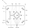
図1〜図6は、本発明の第1実施形態の半導体発光装置の一例およびこれに用いられるLEDチップの一例を示している。本実施形態の半導体発光装置A1は、ケース2、複数のLEDチップ5、ツェナーダイオード6、および封止樹脂7を備えている。なお、図1においては、理解の便宜上封止樹脂7を省略している。
FIGS. 1-6 has shown an example of the semiconductor light-emitting device of 1st Embodiment of this invention, and an example of the LED chip used for this. The semiconductor light emitting device A1 of this embodiment includes a
ケース2は、半導体発光装置A1の土台となるものであり、基材3と配線4とを有している。ケース2のサイズは、平面視寸法が5〜10mm角程度、厚さが1.0mm程度とされている。
The
基材3は、平面視略矩形状の厚板状とされており、たとえばアルミナなどのセラミックからなる。本実施形態においては、このセラミックとして、低温同時焼成セラミックと称される、焼成温度が900℃程度と比較的低い材質が用いられている。この低温同時焼成セラミックは、低焼成温度により、配線4の材質となる金属と同時に焼成することが可能である。基材3の中央には、収容凹部33が形成されている。収容凹部33は、複数のLEDチップ5を収容しており、平面視形状が円形とされている。基材3の四隅には、コーナー凹部34が形成されている。コーナー凹部34は、半導体発光装置A1の製造方法において、セラミック材料を適切分割するために設けられた貫通孔の一部であり、断面四半円形状の溝とされている。基材3は、表面31と裏面32とを有している。本実施形態においては、収容凹部33の深さが、たとえば0.6mm程度とされている。
The
配線4は、複数のLEDチップ5に対して直流電力を供給するための経路として用いられるものであり、表面層41、中間層42、裏面層43、複数のアノード貫通配線44、および複数のカソード貫通配線45を有している。
The
図4は、図2のIV−IV線に沿う平面で半導体発光装置A1を切断したと仮定した場合の要部平面図である。本発明においては、便宜上、配線4のうち、収容凹部33に囲まれた円形の表面31と、基材3の厚さ方向において表面31と同位に存在する面とに形成された部位を、表面層41と称している。
FIG. 4 is a plan view of a principal part when it is assumed that the semiconductor light emitting device A1 is cut along a plane along line IV-IV in FIG. In the present invention, for the sake of convenience, a portion of the
表面層41は、複数のアノードパッド41a、複数のカソードパッド41b、バイパスカソードパッド41c、バイパスアノードパッド41d、アノードメッキ配線41e、およびカソードメッキ配線41fを含んでいる。本実施形態においては、表面層41のうちアノードメッキ配線41eおよびカソードメッキ配線41fを除く部分がAuからなり、アノードメッキ配線41eおよびカソードメッキ配線41fは、Auを含む適宜選択された金属からなる。
The
複数のアノードパッド41aおよび複数のカソードパッド41bは、LEDチップ5を実装するためのものである。図4によく表れているように、アノードパッド41aとカソードパッド41bとは隣り合う組として配置されている。本実施形態においては、アノードパッド41aとカソードパッド41bとの組が、5組形成されている。各アノードパッド41aは、3本の平行な枝状部分と、これらの枝状部分に対して直角につながる帯状部分と、この帯状部分につながる円形部分とを有している。カソードパッド41bは、帯状部分とこの帯状部分につながる円形部分とを有している。
The plurality of
バイパスカソードパッド41cとバイパスアノードパッド41dは、LEDチップ5に過大な逆電圧が印加されることを回避するためのバイパス機能素子を実装するためのものであり、本実施形態においては、バイパス機能素子としてツェナーダイオード6が実装されている。バイパスカソードパッド41cは、円形状とされており、バイパスアノードパッド41dは、矩形状部分とこの矩形状部分につながる円形部分とを有している。
The
アノードメッキ配線41eおよびカソードメッキ配線41fは、複数のアノードパッド41a、複数のカソードパッド41b、バイパスカソードパッド41c、バイパスアノードパッド41d、および裏面層43をメッキによって形成するために用いられるものである。アノードメッキ配線41eおよびカソードメッキ配線41fは、図4における基材3の図中上端から下端にわたって、互いにほぼ平行に延びている。
The
中間層42は、基材3の厚さ方向において表面31と裏面32とのほぼ中央(表面31から深さ0.2mm程度)に形成されている。図5は、図2のV−V線に沿う平面に沿って半導体発光装置A1を切断したと仮定した場合の要部平面図である。本図に示すように、中間層42は、カソード中継配線42aを含んでいる。カソード中継配線42aは、略五角形の部分と、この五角形部分につながる帯状部分と、この帯状部分に対して直角につながる帯状部分とを有している。
The
図6に示すように、裏面層43は、基材3の裏面32に形成されており、アノード実装電極43aとカソード実装電極43bとを有している。アノード実装電極43aおよびカソード実装電極43bは、半導体発光装置A1をたとえば回路基板などに面実装するために用いられる。本実施形態においては、アノード実装電極43aおよびカソード実装電極43bは、Auからなる。アノード実装電極43aは、略矩形状であり、図6において基材3の裏面32の右側2/3程度の領域を覆っている。カソード実装電極43bは、長矩形状であり、裏面32の左側1/4程度の領域を覆っている。
As shown in FIG. 6, the
複数のアノード貫通配線44は、複数の全厚アノード貫通配線44a、複数のメッキ用アノード貫通配線44b、およびバイパスカソード貫通配線44cを含んでいる。複数のアノード貫通配線44はそれぞれ、Ag、Ta、もしくはハンダからなり、本実施形態においてはAgからなる。図2に示すように全厚アノード貫通配線44aは、基材3を表面31から裏面32までその厚さ方向に貫通している。図4および図6から理解される通り、複数の全厚アノード貫通配線44aは、基材3の厚さ方向視において複数のアノードパッド41aおよびアノード実装電極43aの双方に重なっている。すなわち、各全厚アノード貫通配線44aは、その表面31側の端面が、アノードパッド41aの円形部分によって覆われており、裏面32側の端面が、アノード実装電極43aによって覆われている。
The plurality of anode through
複数のメッキ用アノード貫通配線44bは、基材3をその厚さ方向において全厚アノード貫通配線44aと同じ領域を貫通している。図4および図6から理解される通り、複数のメッキ用アノード貫通配線44bは、基材3の厚さ方向視においてアノードメッキ配線41eおよびアノード実装電極43aの双方に重なっている。すなわち、各メッキ用アノード貫通配線44bは、その表面31側の端面が、アノードメッキ配線41eによって覆われており、裏面32側の端面が、アノード実装電極43aによって覆われている。
The plurality of
バイパスカソード貫通配線44cは、全厚アノード貫通配線44aと同様に基材3を表面31から裏面32までその厚さ方向に貫通している。図4および図6から理解される通り、バイパスカソード貫通配線44cは、基材3の厚さ方向視においてバイパスカソードパッド41cおよびアノード実装電極43aの双方に重なっている。すなわち、バイパスカソード貫通配線44cは、その表面31側の端面が、バイパスカソードパッド41cによって覆われており、裏面32側の端面が、アノード実装電極43aによって覆われている。
The bypass cathode through
複数のカソード貫通配線45は、複数の表面側カソード貫通配線45a、複数の裏面側カソード貫通配線45b、複数のメッキ用カソード貫通配線45c、およびバイパスアノード貫通配線45dを含んでおり、本実施形態においてはAgからなる。図2に示すように、表面側カソード貫通配線45aは、基材3のうちその厚さ方向において表面31から中間層42までの部分を貫通している。図4および図5から理解される通り、複数の表面側カソード貫通配線45aは、基材3の厚さ方向視において複数のカソードパッド41bおよびカソード中継配線42aと重なっている。すなわち、複数の表面側カソード貫通配線45aは、その表面31側の端面が複数のカソードパッド41bによって覆われており、中間層42側の端面がカソード中継配線42aによって覆われている。
The plurality of cathode through
複数の裏面側カソード貫通配線45bは、基材3のうちその厚さ方向において中間層42から裏面32までの部分を貫通している。図5および図6から理解される通り、複数の裏面側カソード貫通配線45bは、基材3の厚さ方向視においてカソード中継配線42aおよびカソード実装電極43bと重なっている。すなわち、複数の裏面側カソード貫通配線45bは、その中間層42側の端面がカソード中継配線42aによって覆われており、裏面32側の端面がカソード実装電極43bによって覆われている。中間層42のカソード中継配線42aを介して、複数の表面側カソード貫通配線45aと複数の裏面側カソード貫通配線45bとは互いに導通している。
The plurality of back surface side cathode penetration wirings 45 b penetrate through a portion from the
複数のメッキ用カソード貫通配線45cは、基材3をその厚さ方向において全厚アノード貫通配線44aと同じ領域を貫通している。図4および図6から理解される通り、複数のメッキ用カソード貫通配線45cは、基材3の厚さ方向視においてカソードメッキ配線41fおよびカソード実装電極43bの双方に重なっている。すなわち、各メッキ用カソード貫通配線45cは、その表面31側の端面が、カソードメッキ配線41fによって覆われており、裏面32側の端面が、カソード実装電極43bによって覆われている。
The plurality of
バイパスアノード貫通配線45dは、表面側カソード貫通配線45aと同様に基材3を表面31から中間層42までを貫通している。図4および図5から理解される通り、バイパスアノード貫通配線45dは、基材3の厚さ方向視においてバイパスアノードパッド41dおよびカソード中継配線42aの双方に重なっている。すなわち、バイパスアノード貫通配線45dは、その表面31側の端面が、バイパスアノードパッド41dによって覆われており、中間層42側の端面が、カソード中継配線42aによって覆われている。
The bypass anode through
半導体発光装置A1の光源となる複数のLEDチップ5のそれぞれは、以下のように構成されている。まず、たとえばサファイアからなる基板5a上に、たとえばGaN系半導体からなるn型半導体層5bが積層されている。さらに、n型半導体層5b上に活性層5cが積層されている。活性層5cは、たとえばGaN系半導体からなる複数の層が積層された多重量子井戸構造とされている。p型半導体層5dは、活性層5c上に積層されており、たとえはGaN系半導体からなる。アノード電極5eは、p型半導体層5d上に積層されており、たとえばAl,Au,Ag等の金属からなる。カソード電極5fは、p型半導体層5dおよび活性層5cをエッチングにより取り除くことによって露出したn型半導体層5b上に積層されており、たとえばAl,Au,Ag等の金属からなる。
Each of the plurality of
個々のLEDチップ5は、それぞれが製造されたのちに、上下を反転させたいわゆるフリップチップと称される実装形態で、アノードパッド41aおよびカソードパッド41bに実装されている。詳細には、アノード電極5eは、接合部51を介してアノードパッド41aに接続されており、カソード電極5fは、接合部51を介してカソードパッド41bに接続されている。このような構成のLEDチップ5からは、たとえば青色光が発せられる。
Each
ツェナーダイオード6は、LEDチップ5に過大な逆電圧が印加されることを回避するための機能素子であり、本実施形態においては、バイパスカソードパッド41cにダイボンディングされており、バイパスカソードパッド41cに導通している。またツェナーダイオード6とバイパスアノードパッド41dとは、ワイヤ61によって接続されている。なお、ツェナーダイオード6に代えて、逆電圧印加を回避する機能素子として、バリスタ素子やESD(Electro Static Discharge)保護素子を用いてもよい。
The
封止樹脂7は、ケース2の収容凹部33を埋めており、複数のLEDチップ5を覆っている。封止樹脂7は、透明なエポキシ樹脂またはシリコーン樹脂に蛍光材料が混入された材質からなる。この蛍光材料は、LEDチップ5からの青色光によって励起されることにより、たとえば黄色光を発する。この黄色光と青色光とが混色されることにより、半導体発光装置A1からは白色光が出射される。
The sealing
次に、半導体発光装置A1の作用について説明する。 Next, the operation of the semiconductor light emitting device A1 will be described.
本実施形態によれば、図2および図3に示すように、活性層5cとケース2との間には、基板5aは介在していない。基板5aと比較して、p型半導体層5dはごく薄く、アノード電極5eは、熱伝導率が高い金属からなる。このため、LEDチップ5が点灯したときに発生する熱は、ケース2へと伝わりやすい。したがって、LEDチップ5からの放熱を促進することが可能であり、LEDチップ5の発光効率を高めることができる。
According to the present embodiment, as shown in FIGS. 2 and 3, the
アノードパッド41aは、全厚アノード貫通配線44aを介してアノード実装電極43aにつながっている。このため、LEDチップ5からの熱は、全厚アノード貫通配線44aを通じてアノード実装電極43a、さらには半導体発光装置A1が実装されたたとえば回路基板へと伝えられる。これは、LEDチップ5の放熱を促進し、LEDチップ5の発光効率を高めるのに適している。
The
また、カソードパッド41bは、表面側カソード貫通配線45a、カソード中継配線42a、および裏面側カソード貫通配線45bを介してカソード実装電極43bにつながっている。このため、LEDチップ5からの熱は、表面側カソード貫通配線45a、カソード中継配線42a、および裏面側カソード貫通配線45bを通じてカソード実装電極43b、さらには半導体発光装置A1が実装されたたとえば回路基板へと伝えられる。これは、LEDチップ5の放熱を促進し、LEDチップ5の発光効率を高めるのに適している。
The
複数のアノード貫通配線44および複数のカソード貫通配線45は、Agからなる。これは、LEDチップ5からの放熱を促進するのに有利である。また、複数のアノード貫通配線44および複数のカソード貫通配線45は、表面31側および裏面32側の端面が、表面層41および裏面層43によって覆われている。表面層41および裏面層43のうち、少なくともこれらの端面を覆う部分は、Auによって形成されている。これにより、比較的変質しやすいAgからなる複数のアノード貫通配線44および複数のカソード貫通配線45を適切に保護することができる。
The plurality of anode through
基材3は、アルミナなどのセラミックからなり、LEDチップ5の材料であるたとえばGaN系半導体と熱膨張率が比較的近似している。このため、LEDチップ5をケース2に実装する作業や、LEDチップ5の発光時などに、LEDチップ5とケース2との間に熱膨張差が生じにくい。これにより、LEDチップ5がケース2から不当にはがれてしまうことを防止することができる。
The
バイパスカソードパッド41cは、バイパスカソード貫通配線44cを介してアノード実装電極43aにつながっている。これは、LEDチップ5に過大な逆電圧が印加されるのを回避するために、一時的な大電流をスムーズに流すのに適している。
The
図7〜図9を用いて、本発明の第2実施形態について説明する。 A second embodiment of the present invention will be described with reference to FIGS.
同図に示す半導体発光装置A2は、図9の充填部8を備える点において、半導体発光装置A1における構成と主に異なる。具体的には以下のとおりである。 The semiconductor light emitting device A2 shown in the figure is mainly different from the configuration of the semiconductor light emitting device A1 in that it includes the filling portion 8 of FIG. Specifically, it is as follows.
半導体発光装置A1の説明では省略したが、実際には、アノード貫通配線44やカソード貫通配線45には、基材3の裏面32側に凹む凹部が形成される場合が多い。このような凹部は基材3を焼成する際に形成される。図9に、アノード貫通配線44のうちの全厚アノード貫通配線44aに形成された凹部44hを示している。本実施形態においては、図7、図8に示すように、全厚アノード貫通配線44aに重なる位置に、複数のLEDチップ5がそれぞれ配置されている。
Although omitted in the description of the semiconductor light emitting device A1, in practice, the anode through
なお、本実施形態においては、一つのLEDチップ5と重なる位置に全厚アノード貫通配線44aが3つ形成されているが、一つのLEDチップ5に重なる全厚アノード貫通配線44aの個数は3つに限られず、1つや2つでもよいし、4つ以上でもよい。全厚アノード貫通配線44aの数が多いと、LEDチップ5からの熱をより効率良くアノード実装電極43aに伝えることができる。このことは、半導体発光装置A2の放熱性向上の観点から好ましい。また、全厚アノード貫通配線44aの数が多いことは、表面層41(アノードパッド41a)とアノード実装電極43aとの間の電気抵抗を減少させるのに適する。
In this embodiment, three full thickness anode through
凹部44hを規定する表面は表面層41に覆われている。表面層41は全体にわたってほぼ均一な厚さである。そのため、表面層41にも凹部41hが形成されている。図9に示す凹部41hは、表面層41のうちアノードパッド41aに形成されている。凹部41hは、基材3の裏面32側に凹んでいる。凹部41hは、基材3の厚さ方向視において凹部44hに重なる。そのため、図9では、凹部41hは凹部44hの真上に位置している。なお特に図示しないが、本実施形態において表面層41は、Niよりなる層と、Auよりなる層とが積層された構造を有する。Niよりなる層は、Auよりなる層および基材3の間に介在している。
The surface defining the
充填部8は凹部41hに充填されている。充填部8は、表面層41および接合部51に接している。充填部8は、導電性の材料よりなっていてもよいし、絶縁性の材料よりなっていてもよい。本実施形態では、充填部8は導電性の材料よりなる。充填部8を構成する導電性の材料としては、たとえば、AuとSnとの合金が挙げられる。充填部8は、LEDチップ5を接合部51を介して表面層41に配置する前に形成される。充填部8の形成は、たとえば、凹部41hにペーストを塗布することにより行う。
The filling portion 8 is filled in the
本実施形態においても接合部51は、複数のLEDチップ5のいずれか一つと、表面層41との間に介在している。接合部51は、各LEDチップ5を表面層41に接合するためのものである。接合部51は、導電性の材料よりなっていてもよいし、絶縁性の材料よりなっていてもよい。本実施形態では、接合部51は導電性の材料よりなる。接合部51を構成する導電性の材料としては、たとえば、AuとSnとの合金が挙げられる。本実施形態とは異なり、接合部51を構成する導電性の材料は、銀ペーストやハンダであってもよい。
Also in the present embodiment, the
半導体発光装置A2によると、LEDチップ5を基材3に配置する前に、充填部8を凹部41hに形成することで、LEDチップ5が配置されるべき部位の表面をより平坦にすることができる。そのため、全厚アノード貫通配線44aに基材3の厚さ方向視において重なる位置にLEDチップ5を配置したとしても、LEDチップ5が凹部41hにはまり込まないから、LEDチップ5を配置する際にLEDチップ5の姿勢が崩れることを防止できる。したがって、半導体発光装置A2の製造上の歩留まりの向上を図ることができる。
According to the semiconductor light emitting device A2, before the
なお、図9では、アノード貫通配線44に凹部44hが形成されており、表面層41のうちのアノードパッド41aに凹部41hが形成されている例を示した。図9に示したのと異なり、図10に示すように、カソード貫通配線45に凹部45hが形成されており、この凹部45hと基材3の厚さ方向視において重なる位置に凹部41hが形成されている場合も考えられる。この場合に、凹部41hに充填部8を形成し、カソード貫通配線45と基材3の厚さ方向視において重なる位置に、LEDチップを配置してもよい。
FIG. 9 shows an example in which the
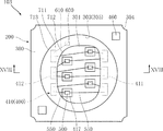
図11〜図13は、本発明の第3実施形態に基づく半導体発光装置を示している。本実施形態の半導体発光装置101は、ケース200、複数のLEDチップ500、ツェナーダイオード600、反射樹脂710、および封止樹脂700を備えている。なお、図11においては、理解の便宜上封止樹脂700を省略している。
11 to 13 show a semiconductor light emitting device according to a third embodiment of the present invention. The semiconductor
ケース200は、半導体発光装置101の土台となるものであり、基材300と配線400とを有している。ケース200のサイズは、平面視寸法が5〜10mm角程度、厚さが1.0mm程度とされている。
The
基材300は、平面視略矩形状の厚板状とされており、たとえばアルミナなどのセラミックからなる。本実施形態においては、このセラミックとして、低温同時焼成セラミックと称される、焼成温度が900℃程度と比較的低い材質が用いられている。この低温同時焼成セラミックは、低焼成温度により、配線400の材質となる金属と同時に焼成することが可能である。
The
基材300の中央には、収容凹部303が形成されている。収容凹部303は、複数のLEDチップ500を収容しており、平面視形状が矩形状とされている。基材300の四隅には、コーナー凹部304が形成されている。コーナー凹部304は、半導体発光装置101の製造方法において、セラミック材料を適切分割するために設けられた貫通孔の一部であり、断面四半円形状の溝とされている。基材300は、表面301と裏面302とを有している。収容凹部303の内壁面305は、環状であり、表面301に対して直角である。本実施形態においては、収容凹部303の深さが、たとえば0.6mm程度とされている。
An
基材300は、せき止め凹部306を有している。せき止め凹部306は、表面301から凹んでおり、内壁面305に接している。本実施形態においては、せき止め凹部306は矩形状とされている。
The
配線400は、複数のLEDチップ500に対して直流電力を供給するための経路として用いられるものであり、表面層410、中間層420、裏面層430、複数のアノード貫通配線440、および複数のカソード貫通配線450を有している。
The
表面層410は、複数のアノードパッド411、複数のカソードパッド412、バイパスカソードパッド413、およびバイパスアノードパッド414を含んでいる。表面層410は、たとえばAuからなる。
The
複数のアノードパッド411および複数のカソードパッド412は、LEDチップ500を実装するためのものである。アノードパッド411とカソードパッド412とは隣り合う組として配置されている。本実施形態においては、アノードパッド411とカソードパッド412との組が、5組形成されている。各アノードパッド411は、3本の平行な枝状部分と、これらの枝状部分に対して直角につながる帯状部分と、この帯状部分につながる円形部分とを有している。カソードパッド412は、帯状部分とこの帯状部分につながる円形部分とを有している。
The plurality of
バイパスカソードパッド413とバイパスアノードパッド414は、LEDチップ500に過大な逆電圧が印加されることを回避するためのバイパス機能素子を実装するためのものであり、本実施形態においては、バイパス機能素子としてツェナーダイオード600が実装されている。バイパスカソードパッド413は、円形状とされており、バイパスアノードパッド414は、矩形状部分とこの矩形状部分につながる円形部分とを有している。
The
中間層420は、基材300の厚さ方向において表面301と裏面302とのほぼ中央(表面301から深さ0.2mm程度)に形成されている。中間層420は、カソード中継配線421を含んでいる。
The
図12に示すように、裏面層430は、基材300の裏面302に形成されており、アノード実装電極431とカソード実装電極432とを有している。アノード実装電極431およびカソード実装電極432は、半導体発光装置101をたとえば回路基板などに面実装するために用いられる。本実施形態においては、アノード実装電極431およびカソード実装電極432は、Auからなる。アノード実装電極431は、略矩形状であり、基材300の裏面302の図中右側2/3程度の領域を覆っている。カソード実装電極432は、長矩形状であり、裏面302の図中左側1/4程度の領域を覆っている。
As shown in FIG. 12, the
複数のアノード貫通配線440は、複数の全厚アノード貫通配線441およびバイパスカソード貫通配線443を含んでいる。複数のアノード貫通配線440はそれぞれ、Ag、Ta、もしくはハンダからなり、本実施形態においてはAgからなる。図13に示すように全厚アノード貫通配線441は、基材300を表面301から裏面302までその厚さ方向に貫通している。各全厚アノード貫通配線441は、その表面301側の端面が、アノードパッド411の円形部分によって覆われており、裏面302側の端面が、アノード実装電極431によって覆われている。
The plurality of anode through
バイパスカソード貫通配線443は、全厚アノード貫通配線441と同様に基材300を表面301から裏面302までその厚さ方向に貫通している。バイパスカソード貫通配線443は、その表面301側の端面が、バイパスカソードパッド413によって覆われており、裏面302側の端面が、アノード実装電極431によって覆われている。
The bypass cathode through
複数のカソード貫通配線450は、複数の表面側カソード貫通配線451、複数の裏面側カソード貫通配線(図示略)、およびバイパスアノード貫通配線(図示略)を含んでおり、本実施形態においてはAgからなる。表面側カソード貫通配線451は、基材300のうちその厚さ方向において表面301から中間層420までの部分を貫通している。表面側カソード貫通配線451は、その表面301側の端面が複数のカソードパッド412によって覆われており、中間層420側の端面がカソード中継配線421によって覆われている。上記裏面側カソード貫通配線は、基材300のうちその厚さ方向において中間層420から裏面302までの部分を貫通している。上記裏面側カソード貫通配線は、その中間層420側の端面がカソード中継配線421によって覆われており、裏面302側の端面がカソード実装電極432によって覆われている。中間層420のカソード中継配線421を介して、複数の表面側カソード貫通配線451と上記複数の裏面側カソード貫通配線とは互いに導通している。上記バイパスアノード貫通配線は、表面側カソード貫通配線451と同様に基材300を表面301から中間層420までを貫通している。バイパスアノード貫通配線は、その表面301側の端面が、バイパスアノードパッド414によって覆われており、中間層420側の端面が、カソード中継配線421によって覆われている。
The plurality of cathode through
基材300の最上面には、2つのテスト電極460が形成されている。これらのテスト電極460は、複数のアノードパッド411および複数のカソードパッド412と導通している。半導体発光装置101の製造工程においては、テスト用の電源プローブを2つのテスト電極460に接触させることにより、LEDチップ500の点灯テストを行うことができる。
Two
半導体発光装置101の光源となる複数のLEDチップ500のそれぞれは、以下のように構成されている。まず、図14に示すようにたとえばサファイアからなる基板501上に、たとえばGaN系半導体からなるn型半導体層502が積層されている。さらに、n型半導体層502上に活性層503が積層されている。活性層503は、たとえばGaN系半導体からなる複数の層が積層された多重量子井戸構造とされている。p型半導体層504は、活性層503上に積層されており、たとえはGaN系半導体からなる。アノード電極505は、p型半導体層504上に積層されており、たとえばAl,Au,Ag等の金属からなる。カソード電極506は、p型半導体層504および活性層503をエッチングにより取り除くことによって露出したn型半導体層502上に積層されており、たとえばAl,Au,Ag等の金属からなる。
Each of the plurality of
個々のLEDチップ500は、それぞれが製造されたのちに、上下を反転させたいわゆるフリップチップと称される実装形態で、アノードパッド411およびカソードパッド412に実装されている。詳細には、アノード電極505は、接合部510を介してアノードパッド411に接続されており、カソード電極506は、接合部510を介してカソードパッド412に接続されている。このような構成のLEDチップ500からは、たとえば青色光が発せられる。
Each
ツェナーダイオード600は、LEDチップ500に過大な逆電圧が印加されることを回避するためのバイパス機能素子であり、本実施形態においては、バイパスカソードパッド413にダイボンディングされており、バイパスカソードパッド413に導通している。またツェナーダイオード600とバイパスアノードパッド414とは、ワイヤ610によって接続されている。ツェナーダイオード600、バイパスカソードパッド413、およびバイパスアノードパッド414は、せき止め凹部306内に形成されている。なお、ツェナーダイオード600に代えて、逆電圧印加を回避するバイパス機能素子として、バリスタ素子やESD(Electro Static Discharge)保護素子を用いてもよい。
The
反射樹脂710は、たとえばシリコーン樹脂に酸化チタンが混入された材料からなり、鮮やかな白色を呈する。図11および図13に示すように、反射樹脂710は、内縁712、外縁713、および反射面711を有している。内縁712は、複数のLEDチップ500から離間した位置において、これらを囲んでいる。外縁713は、内壁面305と接している。反射面711は、内縁712と外縁713とを繋ぐ面であり、内縁712から外縁713に向かうほど表面301からの高さが高い傾斜面とされている。内縁712は、表面301に接している。また、表面301から外縁713までの高さaは、表面301からLEDチップ500の活性層503までの高さbよりも高い。反射樹脂710は、ツェナーダイオード600、バイパスカソードパッド413、バイパスアノードパッド414、およびワイヤ610を覆っている。内縁712の一部は、せき止め凹部306の端縁の一部と一致している。反射樹脂710は、たとえば適度な粘性を有する樹脂材料を表面301およびせき止め凹部306に付着させることによって形成できる。この樹脂材料の流動および表面張力によって、上述した反射樹脂710の形状が実現される。
The
封止樹脂700は、ケース200の収容凹部303を埋めており、複数のLEDチップ500および反射樹脂710を覆っている。封止樹脂700は、透明なエポキシ樹脂またはシリコーン樹脂に蛍光材料が混入された材質からなる。この蛍光材料は、LEDチップ500からの青色光によって励起されることにより、たとえば黄色光を発する。この黄色光と青色光とが混色されることにより、半導体発光装置101からは白色光が出射される。
The sealing
次に、半導体発光装置101の作用について説明する。
Next, the operation of the semiconductor
本実施形態によれば、図13に示すように、LEDチップ500と内壁面305との間には、反射面711が存在する。反射面711は、LEDチップ500側の内縁712から内壁面305と接する外縁713に向かって、表面301からの高さが徐々に高くなるように傾斜している。これにより、LEDチップ500から側方に出射した光を図中上方へと適切に向かわせることができる。また、反射面711は、収容凹部303内に設けた反射樹脂710によって構成されている。このため、反射樹脂710を設けることによっては、ケース200のサイズを大きくする必要がない。したがって、半導体発光装置101の高輝度化と小型化とを図ることができる。
According to the present embodiment, as shown in FIG. 13, the
反射樹脂710は、基材300の材料であるセラミックよりも反射率が高い材料からなる。これにより、LEDチップ500からの光が反射面711によって反射されるときの減衰を抑制することができる。反射樹脂710の材料として、白色樹脂を用いることは、反射による減衰を抑制するのに好適である。
The
活性層503は、LEDチップ500における発光部位である。図13および図15に示すように、表面301から外縁713までの高さaは、表面301から活性層503までの高さbよりも高い。このため、活性層503から側方に出射された光の正面には、反射面711が位置している。したがって、活性層503から側方に出射された光を上方へと効率よく反射することができる。
The
内壁面305が表面301に対して直角であることは、ケース200の小型化に有利である。
The fact that the
一般的に、ツェナーダイオード600は、白色樹脂からなる反射樹脂710と比べてより多くの光を吸収する。このツェナーダイオード600を反射樹脂710によって覆うことにより、LEDチップ500からの光がツェナーダイオード600に吸収されることを防止可能であり、半導体発光装置101の高輝度化をさらに促進することができる。せき止め凹部306にツェナーダイオード600を配置することにより、反射樹脂710を形成する際に、液状あるいはペースト状の樹脂材料をせき止め凹部306に付着させると、この樹脂材料によってツェナーダイオード600を適切に覆いつつ、内縁712がせき止め凹部306の端縁を超えることを表面張力によって回避することができる。これは、高輝度化を図る一方、反射樹脂710がLEDチップ500のたとえば活性層503に付着してしまうことを防止するのに適している。
In general, the
図15〜図22は、本発明の他の実施形態を示している。なお、これらの図において、上記実施形態と同一または類似の要素には、上記実施形態と同一の符号を付している。 15 to 22 show another embodiment of the present invention. In these drawings, the same or similar elements as those in the above embodiment are denoted by the same reference numerals as those in the above embodiment.
図15および図16は、本発明の第4実施形態に基づく半導体発光装置を示している。本実施形態の半導体発光装置102は、せき止め凹部306の構成が上述した実施形態と異なっている。
15 and 16 show a semiconductor light emitting device according to the fourth embodiment of the present invention. The semiconductor
本実施形態においては、せき止め凹部306は、包囲部307および突出部308を有している。包囲部307は、内壁面305に沿った環状であり、複数のLEDチップ500を囲んでいる。突出部308は、包囲部307から互いに隣り合うLEDチップ500どうしの間に突出している。突出部308の先端よりもケース200の中央寄り領域には、1つのLEDチップ500が配置されている。
In the present embodiment, the dammed
本実施形態においては、反射樹脂710の内縁712すべてが、せき止め凹部306の端縁と一致している。すなわち、反射樹脂710は、表面301から退避した位置に設けられている。
In the present embodiment, all of the
このような実施形態によっても、半導体発光装置102の高輝度化と小型化をと図ることができる。また、せき止め凹部306に包囲部307を設けることにより、反射樹脂710の内縁712をLEDチップ500に対してより近い位置に設けるとともに、反射樹脂710を形成する際に誤ってLEDチップ500に樹脂材料が付着してしまうことを防止することができる。突出部308を設けることにより、隣り合うLEDチップ500どうしに挟まれたスペースに、反射樹脂710を適切に形成することができる。反射面711のうち突出部308によって延長された部分は、中央に位置するLEDチップ500からの光を効率よく反射することができる。
Even in such an embodiment, the semiconductor
図17および図18は、本発明の第5実施形態に基づく半導体発光装置を示している。本実施形態の半導体発光装置103は、主にLEDチップ500の構成が上述した実施形態と異なっている。本実施形態においては、図19に示すように、LEDチップ500は、アノード電極505およびカソード電極506が上面側に形成されている。そして、これらのアノード電極505およびカソード電極506にワイヤ550が接続されている。このようなLEDチップ500は、いわゆる2ワイヤタイプと称される。
17 and 18 show a semiconductor light emitting device according to a fifth embodiment of the present invention. The semiconductor
図17に示すように、収容凹部303は、平面視円形状である。表面301には、複数のダイボンディングパッド417が形成されている。ダイボンディングパッド417には、LEDチップ500がダイボンディングされている。複数のダイボンディングパッド417を挟んで、複数のアノードパッド411と複数のカソードパッド412が配置されている。各アノードパッド411および各カソードパッド412には、ワイヤ550が接続されている。
As shown in FIG. 17, the
反射樹脂710は、複数のアノードパッド411および複数のカソードパッド412を覆っている。また、ワイヤ550は、複数のアノードパッド411および複数のカソードパッド412側の部分が反射樹脂710によって覆われている。内縁712は、複数のLEDチップ500および複数のダイボンディングパッド417から離間した位置においてこれらを囲んでいる。ツェナーダイオード600、ワイヤ610も、反射樹脂710に覆われている。
The
このような実施形態によっても、半導体発光装置103の高輝度化と小型化をと図ることができる。また、アノードパッド411およびカソードパッド412は、LEDチップ500に対して外側に配置されている。このため、2ワイヤタイプであるLEDチップ500に接続されたワイヤ550は、いずれもLEDチップ500に対して外側に延びる。ワイヤ550のうちアノードパッド411およびカソードパッド412にボンディングされた部分およびその近傍部分は、反射樹脂710を形成する際に、表面張力によって樹脂材料を引き寄せる機能を果たす。これにより、樹脂材料をLEDチップ500に対して外側に滞留させることができる。
Even in such an embodiment, the semiconductor
図20および図21は、本発明の第6実施形態に基づく半導体発光装置を示している。本実施形態の半導体発光装置104は、主に、ケース200の全体構成、LEDチップ500の構造が、上述した実施形態と異なっている。
20 and 21 show a semiconductor light emitting device according to a sixth embodiment of the present invention. The semiconductor
本実施形態においては、図22に示すように、LEDチップ500は、たとえばSiからなるサブマウント基板507と、基板501、たとえばGaNからなるn型半導体層502、活性層503およびp型半導体層504が積層された半導体層とを有する構造とされており、たとえば青色光を発する。上記半導体層には、サブマウント基板507側にアノード電極505およびカソード電極506が形成されている。これらのアノード電極505およびカソード電極506は、サブマウント基板507に形成された配線パターン(図示略)に導電性ペースト511によって接合されている。サブマウント基板507には2つの電極(図示略)が形成されている。これらの電極には、2つのワイヤ550それぞれの一端がボンディングされている。図20および図21に示すように、一方のワイヤ550の他端は、アノードパッド411にボンディングされており、他方のワイヤ550の他端は、カソードパッド412にボンディングされている。
In the present embodiment, as shown in FIG. 22, the
基材300は、平面視長矩形状とされており、収容凹部303も長矩形状である。本実施形態においては、内壁面305が表面301と直角である方向に対して傾いている。反射樹脂710は、表面301のうちLEDチップ500のサブマウント基板507が接合された部分以外の領域を覆っている。反射樹脂710の内縁712は、サブマウント基板507に接している。アノードパッド411は、収容凹部303のほとんどを占める平面視寸法とされている。複数のLEDチップ500は、アノードパッド411にダイボンディングされている。ツェナーダイオード600、およびワイヤ610は、反射樹脂710に覆われている。なお、サブマウント基板507に、本発明でいうバイパス機能素子が作りこまれた構成としてもよい。
The
基材300の側面には、アノード側面配線461およびカソード側面配線462が形成されている。アノード側面配線461は、アノードパッド411とアノード実装電極431とに繋がっている。カソード側面配線462は、カソードパッド412とカソード実装電極432とに繋がっている。
An anode
このような実施形態によっても、半導体発光装置104の高輝度化と小型化をと図ることができる。収容凹部303内のほとんどを反射樹脂710によって覆うことにより、高輝度化をより促進することができる。サブマウント基板507は、表面301から確実に盛り上がった部位となっている。これにより、反射樹脂710を形成する際に、樹脂材料が活性層503へとはみ出ることを抑制することができる。サブマウント基板507は発光する部位ではないため、半導体発光装置104の高輝度化を阻害することはない。
Also according to such an embodiment, the semiconductor
なお、半導体発光装置104の変形例として、配線400がたとえばCuやFeおよびこれらの合金からなる板状のリードによって形成された構成としてもよい。具体的には、カソードパッド412、カソード側面配線462、およびカソード実装電極432に相当する部位を有するリードと、アノードパッド411、アノード側面配線461、アノード実装電極431に相当する部位を有するリードとを用いる。また、この変形例においては、基材300のうち内壁面305を構成する部分を熱硬化性樹脂または熱可塑性樹脂によって形成することが好ましい。
As a modification of the semiconductor
図23〜図25を用いて、本発明の第7実施形態について説明する。 A seventh embodiment of the present invention will be described with reference to FIGS.
同図に示す半導体発光装置105は、図25の充填部800を備える点において、半導体発光装置101における構成と主に異なる。具体的には以下のとおりである。
The semiconductor
半導体発光装置101の説明では省略したが、実際には、アノード貫通配線440やカソード貫通配線450には、基材300の裏面302側に凹む凹部が形成される場合が多い。このような凹部は基材300を焼成する際に形成される。図25に、アノード貫通配線440のうちの全厚アノード貫通配線441に形成された凹部449を示している。本実施形態においては、図23、図24に示すように、全厚アノード貫通配線441に重なる位置に、複数のLEDチップ500がそれぞれ配置されている。
Although omitted in the description of the semiconductor
なお、本実施形態においては、一つのLEDチップ500と重なる位置に全厚アノード貫通配線441が3つ形成されているが、一つのLEDチップ500に重なる全厚アノード貫通配線441の個数は3つに限られず、1つや2つでもよいし、4つ以上でもよい。全厚アノード貫通配線441の数が多いと、LEDチップ500からの熱をより効率良くアノード実装電極431に伝えることができる。このことは、半導体発光装置105の放熱性向上の観点から好ましい。また、全厚アノード貫通配線441の数が多いことは、表面層410(アノードパッド411)とアノード実装電極431との間の電気抵抗を減少させるのに適する。
In the present embodiment, three full thickness anode through
凹部449を規定する表面は表面層410に覆われている。表面層410は全体にわたってほぼ均一な厚さである。そのため、表面層410にも凹部419が形成されている。図25に示す凹部419は、表面層410のうちアノードパッド411に形成されている。凹部419は、基材300の裏面302側に凹んでいる。凹部419は、基材300の厚さ方向視において凹部449に重なる。そのため図25では、凹部419は凹部449の真上に位置している。なお特に図示しないが、本実施形態において表面層410は、Niよりなる層と、Auよりなる層とが積層された構造を有する。Niよりなる層は、Auよりなる層および基材300の間に介在している。
The surface defining the
充填部800は凹部419に充填されている。充填部800は、表面層410および接合部510に接している。充填部800は、導電性の材料よりなっていてもよいし、絶縁性の材料よりなっていてもよい。本実施形態では、充填部800は導電性の材料よりなる。充填部800を構成する導電性の材料としては、たとえば、AuとSnとの合金が挙げられる。充填部800は、LEDチップ500を接合部510を介して表面層410に配置する前に形成される。充填部800の形成は、たとえば、凹部419にペーストを塗布することにより行う。
The filling
本実施形態においても接合部510は、複数のLEDチップ500のいずれか一つと、表面層410との間に介在している。接合部510は、各LEDチップ500を表面層410に接合するためのものである。接合部510は、導電性の材料よりなっていてもよいし、絶縁性の材料よりなっていてもよい。本実施形態では、接合部510は導電性の材料よりなる。接合部510を構成する導電性の材料としては、たとえば、AuとSnとの合金が挙げられる。本実施形態とは異なり、接合部部510を構成する導電性の材料は、銀ペーストやハンダであってもよい。
Also in the present embodiment, the
半導体発光装置105によると、LEDチップ500を基材300に配置する前に、充填部800を凹部419に形成することで、LEDチップ500が配置されるべき部位の表面をより平坦にすることができる。そのため、全厚アノード貫通配線441に基材300の厚さ方向視において重なる位置にLEDチップ500を配置したとしても、LEDチップ500が凹部419にはまり込まないから、LEDチップ500を配置する際にLEDチップ500の姿勢が崩れることを防止できる。したがって、半導体発光装置105の製造上の歩留まりの向上を図ることができる。
According to the semiconductor
なお、図25では、アノード貫通配線440に凹部449が形成されており、表面層410のうちのアノードパッド411に凹部419が形成されている例を示した。図25に示したのと異なり、図26に示すように、カソード貫通配線450に凹部459が形成されており、この凹部459と基材300の厚さ方向視において重なる位置に凹部419が形成されている場合も考えられる。この場合に、凹部419に充填部800を形成し、カソード貫通配線450と基材300の厚さ方向視において重なる位置に、LEDチップ500を配置してもよい。
FIG. 25 shows an example in which the
また、半導体発光装置102や103にて半導体発光装置105の構成を採用してもよい。
Further, the configuration of the semiconductor
本発明に係る半導体発光装置は、上述した実施形態に限定されるものではない。本発明に係る半導体発光装置の各部の具体的な構成は、種々に設計変更自在である。 The semiconductor light emitting device according to the present invention is not limited to the above-described embodiment. The specific configuration of each part of the semiconductor light emitting device according to the present invention can be varied in design in various ways.
複数のLEDチップの個数は、5個に限定されず、いずれの個数であってもよい。 The number of the plurality of LED chips is not limited to five and may be any number.
A1,A2 半導体発光装置
2 ケース
3 基材
31 表面
32 裏面
33 収容凹部
34 コーナー凹部
4 配線
41 表面層
41a アノードパッド
41b カソードパッド
41c バイパスカソードパッド
41d バイパスアノードパッド
41e アノードメッキ配線
41f カソードメッキ配線
41h 凹部(第2凹部)
42 中間層
42a カソード中継配線
43 裏面層
43a アノード実装電極
43b カソード実装電極
44 アノード貫通配線
44a 全厚アノード貫通配線
44b メッキ用アノード貫通配線
44c バイパスカソード貫通配線
44h 凹部(第1凹部)
45 カソード貫通配線
45a 表面側カソード貫通配線
45b 裏面側カソード貫通配線
45c メッキ用カソード貫通配線
45d バイパスアノード貫通配線
45h 凹部(第1凹部)
5 LEDチップ
5a 基板
5b n型半導体層
5c 活性層
5d p型半導体層
5e アノード電極
5f カソード電極
51 接合部
6 ツェナーダイオード
61 ワイヤ
8 充填部
7 封止樹脂
9 半導体発光装置
91 基材
92 リード
93 LEDチップ
94 半導体層
95 サブマウント基板
96 ワイヤ
97 封止樹脂
a,b 高さ
101,102,103,104,105 半導体発光装置
200 ケース
300 基材
301 表面
302 裏面
303 収容凹部
304 コーナー凹部
305 内壁面
306 せき止め凹部
307 包囲部
308 突出部
400 配線
410 表面層
411 アノードパッド
412 カソードパッド
413 バイパスカソードパッド
414 バイパスアノードパッド
417 ダイボンディングパッド
419 凹部(第2凹部)
420 中間層
421 カソード中継配線
430 裏面層
431 アノード実装電極
432 カソード実装電極
440 アノード貫通配線
441 全厚アノード貫通配線
443 バイパスカソード貫通配線
449 凹部(第1凹部)
450 カソード貫通配線
451 表面側カソード貫通配線
459 凹部(第1凹部)
460 テスト電極
461 アノード側面配線
462 カソード側面配線
500 LEDチップ
501 基板
502 n型半導体層
503 活性層
504 p型半導体層
505 アノード電極
506 カソード電極
507 サブマウント基板
510 接合部
511 導電性ペースト
550 ワイヤ
600 ツェナーダイオード(バイパス機能素子)
610 ワイヤ
700 封止樹脂
710 反射樹脂
711 反射面
712 内縁
713 外縁
800 充填部
A1, A2 Semiconductor light emitting
42
45 Cathode through wiring 45a Front side cathode through
5
a,
420
450 Cathode through
460
610
Claims (32)
上記複数のLEDチップが搭載されたケースと、を備え、
上記各LEDチップは、基板、およびこの基板に積層されたn型半導体層、活性層、p型半導体層、上記p型半導体層に導通するアノード電極および上記n型半導体層に導通するカソード電極を有しており、上記アノード電極および上記カソード電極が上記ケースと対面する姿勢で上記ケースに搭載されており、
上記ケースは、
セラミックからなり、かつ表面および裏面を有する基材と、
上記表面に形成された複数ずつのアノードパッドおよびカソードパッドを含む表面層、上記裏面に形成されたアノード実装電極およびカソード実装電極を含む裏面層、上記複数のアノードパッドと上記アノード実装電極とを導通させ、かつ上記基材の厚さ方向の少なくとも一部を貫通する複数のアノード貫通配線、上記複数のカソードパッドと上記カソード実装電極とを導通させ、かつ上記基材の厚さ方向の少なくとも一部を貫通する複数のカソード貫通配線、を有する配線と、
を有するとともに、
上記複数のアノード貫通配線および上記複数のカソード貫通配線の少なくともいずれかには、第1凹部が形成され、
上記表面層には、上記基材の厚さ方向視において、上記第1凹部に重なる第2凹部が形成され、
上記第2凹部に充填された充填部を更に備え、
上記充填部は、上記基材の厚さ方向視において上記複数のLEDチップのいずれか一つに重なることを特徴とする、半導体発光装置。 A plurality of LED chips;
A case on which the plurality of LED chips are mounted,
Each LED chip includes a substrate, an n-type semiconductor layer, an active layer, a p-type semiconductor layer, an anode electrode connected to the p-type semiconductor layer, and a cathode electrode connected to the n-type semiconductor layer stacked on the substrate. And the anode electrode and the cathode electrode are mounted on the case in a posture facing the case,
The above case
A substrate made of ceramic and having a front surface and a back surface;
A surface layer including a plurality of anode pads and cathode pads formed on the front surface, a back surface layer including anode mounting electrodes and cathode mounting electrodes formed on the back surface, and the plurality of anode pads and anode mounting electrodes are electrically connected. A plurality of through-anode wirings penetrating at least part of the thickness direction of the base material, the plurality of cathode pads and the cathode mounting electrode being electrically connected, and at least a part of the base material in the thickness direction. A plurality of through-cathode wirings that pass through the wiring,
And it has a,
A first recess is formed in at least one of the plurality of anode through wires and the plurality of cathode through wires,
The surface layer is formed with a second recess that overlaps the first recess when viewed in the thickness direction of the substrate.
A filling portion filled in the second recess;
The semiconductor light emitting device, wherein the filling portion overlaps any one of the plurality of LED chips in a thickness direction view of the base material .
上記複数のアノード貫通配線は、上記バイパスカソードパッドと上記アノード実装電極とを導通させるバイパスカソード貫通配線を含んでおり、
上記複数のカソード貫通配線は、上記バイパスアノードパッドと上記カソード実装電極とを導通させるバイパスアノード貫通配線を含んでいる、請求項1ないし請求項15のいずれかに記載の半導体発光装置。 The wiring has a bypass cathode pad and a bypass anode pad formed on the surface,
The plurality of anode through wirings include a bypass cathode through wiring for conducting the bypass cathode pad and the anode mounting electrode,
The semiconductor light-emitting device according to claim 1, wherein the plurality of through-cathode wirings include a bypass anode through wiring that connects the bypass anode pad and the cathode mounting electrode.
上記バイパスアノードパッドと上記ツェナーダイオードとを導通させるワイヤを備える、請求項16に記載の半導体発光装置。 A Zener diode is conductively joined to the bypass cathode pad,
The semiconductor light emitting device according to claim 16, further comprising a wire for conducting the bypass anode pad and the Zener diode.
上記充填部は、上記接合部および上記表面層の間に介在し、且つ、上記接合部および上記表面層のいずれにも接している、請求項1ないし21のいずれかに記載の半導体発光装置。 It further includes a joint portion interposed between any one of the plurality of LED chips and the surface layer,
The semiconductor light emitting device according to any one of claims 1 to 21, wherein the filling portion is interposed between the bonding portion and the surface layer, and is in contact with both the bonding portion and the surface layer.
上記LEDチップが搭載された表面、およびこの表面とは反対側に位置する裏面を有するケースとを備えた半導体発光装置であって、
上記ケースは、上記LEDチップを囲む内壁面を有する基材を含んでおり、
上記LEDチップ側に位置する内縁、上記内壁面に接する外縁、これら内縁および外縁を繋いでおり、かつ上記内縁から上記外縁に向かうほど上記表面から離間するように傾斜した反射面、を有する反射樹脂を備えるとともに、
上記ケースは、表面層、裏面層、複数のアノード貫通配線、および複数のカソード貫通配線を含み、
上記表面層は、上記基材の表面に形成された複数ずつのアノードパッドおよびカソードパッドを含み、
上記裏面層は、上記基材の裏面に形成されたアノード実装電極およびカソード実装電極を含み、
上記複数のアノード貫通配線は、上記複数のアノードパッドと上記アノード実装電極とを導通させ、かつ上記基材の厚さ方向の少なくとも一部を貫通しており、
上記複数のカソード貫通配線は、上記複数のカソードパッドと上記カソード実装電極とを導通させ、かつ上記基材の厚さ方向の少なくとも一部を貫通しており、
上記複数のアノード貫通配線および上記複数のカソード貫通配線の少なくともいずれかには、第1凹部が形成され、
上記表面層には、上記基材の厚さ方向視において、上記第1凹部に重なる第2凹部が形成され、
上記第2凹部に充填された充填部を更に備え、
上記充填部は、上記基材の厚さ方向視において上記複数のLEDチップのいずれか一つに重なることを特徴とする、半導体発光装置。 One or more LED chips;
A semiconductor light emitting device comprising a surface on which the LED chip is mounted, and a case having a back surface opposite to the surface,
The case includes a base material having an inner wall surface surrounding the LED chip,
Reflective resin having an inner edge located on the LED chip side, an outer edge in contact with the inner wall surface, a reflecting surface that connects the inner edge and the outer edge, and is inclined so as to be separated from the surface toward the outer edge from the inner edge provided with a,
The case includes a front surface layer, a back surface layer, a plurality of anode through wires, and a plurality of cathode through wires,
The surface layer includes a plurality of anode pads and cathode pads formed on the surface of the substrate,
The back layer includes an anode mounting electrode and a cathode mounting electrode formed on the back surface of the base material,
The plurality of anode through-wirings conduct the plurality of anode pads and the anode mounting electrode, and penetrate at least part of the thickness direction of the base material,
The plurality of through-cathode wirings conduct the plurality of cathode pads and the cathode mounting electrode, and penetrate at least part of the thickness direction of the base material,
A first recess is formed in at least one of the plurality of anode through wires and the plurality of cathode through wires,
The surface layer is formed with a second recess that overlaps the first recess when viewed in the thickness direction of the substrate.
A filling portion filled in the second recess;
The semiconductor light emitting device, wherein the filling portion overlaps any one of the plurality of LED chips in a thickness direction view of the base material .
上記充填部は、上記接合部および上記表面層の間に介在し、且つ、上記接合部および上記表面層のいずれにも接している、請求項27に記載の半導体発光装置。 It further includes a joint portion interposed between any one of the plurality of LED chips and the surface layer,
28. The semiconductor light emitting device according to claim 27 , wherein the filling portion is interposed between the bonding portion and the surface layer, and is in contact with both the bonding portion and the surface layer.
Priority Applications (7)
| Application Number | Priority Date | Filing Date | Title |
|---|---|---|---|
| JP2011215534A JP5886584B2 (en) | 2010-11-05 | 2011-09-29 | Semiconductor light emitting device |
| US13/289,288 US8648373B2 (en) | 2010-11-05 | 2011-11-04 | Semiconductor light emitting device |
| US14/105,437 US9035333B2 (en) | 2010-11-05 | 2013-12-13 | Semiconductor light emitting device |
| US14/695,915 US9276187B2 (en) | 2010-11-05 | 2015-04-24 | Semiconductor light emitting device |
| US15/018,435 US9496473B2 (en) | 2010-11-05 | 2016-02-08 | Semiconductor light emitting device |
| US15/288,337 US9728523B2 (en) | 2010-11-05 | 2016-10-07 | Semiconductor light emitting device |
| US15/642,501 US10056357B2 (en) | 2010-11-05 | 2017-07-06 | Semiconductor light emitting device |
Applications Claiming Priority (5)
| Application Number | Priority Date | Filing Date | Title |
|---|---|---|---|
| JP2010248494 | 2010-11-05 | ||
| JP2010248494 | 2010-11-05 | ||
| JP2010292644 | 2010-12-28 | ||
| JP2010292644 | 2010-12-28 | ||
| JP2011215534A JP5886584B2 (en) | 2010-11-05 | 2011-09-29 | Semiconductor light emitting device |
Related Child Applications (1)
| Application Number | Title | Priority Date | Filing Date |
|---|---|---|---|
| JP2016024289A Division JP2016086191A (en) | 2010-11-05 | 2016-02-12 | Semiconductor light-emitting device |
Publications (2)
| Publication Number | Publication Date |
|---|---|
| JP2012151436A JP2012151436A (en) | 2012-08-09 |
| JP5886584B2 true JP5886584B2 (en) | 2016-03-16 |
Family
ID=46018770
Family Applications (1)
| Application Number | Title | Priority Date | Filing Date |
|---|---|---|---|
| JP2011215534A Active JP5886584B2 (en) | 2010-11-05 | 2011-09-29 | Semiconductor light emitting device |
Country Status (2)
| Country | Link |
|---|---|
| US (6) | US8648373B2 (en) |
| JP (1) | JP5886584B2 (en) |
Families Citing this family (60)
| Publication number | Priority date | Publication date | Assignee | Title |
|---|---|---|---|---|
| JP2016086191A (en) * | 2010-11-05 | 2016-05-19 | ローム株式会社 | Semiconductor light-emitting device |
| JP6034175B2 (en) * | 2012-01-10 | 2016-11-30 | ローム株式会社 | LED module |
| KR101997243B1 (en) * | 2012-09-13 | 2019-07-08 | 엘지이노텍 주식회사 | Light emtting device and lighting system |
| JP6147977B2 (en) | 2012-09-26 | 2017-06-14 | ローム株式会社 | LED lighting apparatus and LED unit |
| JP6056336B2 (en) * | 2012-09-28 | 2017-01-11 | 日亜化学工業株式会社 | Light emitting device |
| JP6102187B2 (en) | 2012-10-31 | 2017-03-29 | 日亜化学工業株式会社 | Light emitting device package and light emitting device using the same |
| JP2014112669A (en) * | 2012-11-12 | 2014-06-19 | Citizen Holdings Co Ltd | Semiconductor light-emitting device and manufacturing method of the same |
| JP6564159B2 (en) * | 2012-12-07 | 2019-08-21 | 株式会社カネカ | Semiconductor light emitting device |
| JP6107136B2 (en) | 2012-12-29 | 2017-04-05 | 日亜化学工業株式会社 | LIGHT EMITTING DEVICE PACKAGE, LIGHT EMITTING DEVICE INCLUDING THE SAME, AND LIGHTING DEVICE EQUIPPED WITH THE LIGHT EMITTING DEVICE |
| DE102013202904A1 (en) * | 2013-02-22 | 2014-08-28 | Osram Opto Semiconductors Gmbh | Optoelectronic semiconductor component and method for its production |
| CN104037053A (en) * | 2013-03-04 | 2014-09-10 | 海洋王照明科技股份有限公司 | Field emission planar light source |
| JP2014241341A (en) * | 2013-06-11 | 2014-12-25 | 株式会社東芝 | Semiconductor light-emitting device |
| WO2014203825A1 (en) * | 2013-06-18 | 2014-12-24 | ローム株式会社 | Led light source module |
| JP6192377B2 (en) * | 2013-06-18 | 2017-09-06 | ローム株式会社 | LED light source module |
| JP6221403B2 (en) * | 2013-06-26 | 2017-11-01 | 日亜化学工業株式会社 | Light emitting device |
| JP6484396B2 (en) | 2013-06-28 | 2019-03-13 | 日亜化学工業株式会社 | Light emitting device package and light emitting device using the same |
| US9887324B2 (en) | 2013-09-16 | 2018-02-06 | Lg Innotek Co., Ltd. | Light emitting device package |
| JP6331376B2 (en) * | 2013-12-17 | 2018-05-30 | 日亜化学工業株式会社 | Light emitting device manufacturing method and light emitting device |
| KR102299238B1 (en) * | 2014-01-08 | 2021-09-07 | 루미리즈 홀딩 비.브이. | Wavelength converted semiconductor light emitting device |
| CN103794701B (en) * | 2014-01-26 | 2017-01-18 | 广东晶科电子股份有限公司 | LED support and LED device thereof |
| JP6213428B2 (en) * | 2014-03-12 | 2017-10-18 | 豊田合成株式会社 | Light emitting device and manufacturing method thereof |
| US9691949B2 (en) * | 2014-05-30 | 2017-06-27 | Cree, Inc. | Submount based light emitter components and methods |
| TWD167977S (en) * | 2014-06-27 | 2015-05-21 | 隆達電子股份有限公司 | Lead frame for light-emitting diode |
| TWI556478B (en) * | 2014-06-30 | 2016-11-01 | 億光電子工業股份有限公司 | Light emitting diode device |
| US9722160B2 (en) | 2014-10-31 | 2017-08-01 | Nichia Corporation | Light emitting device and adaptive driving beam headlamp system |
| JP6547548B2 (en) * | 2014-10-31 | 2019-07-24 | 日亜化学工業株式会社 | Light emitting device and variable light distribution headlamp system |
| JP6762736B2 (en) * | 2015-03-16 | 2020-09-30 | 晶元光電股▲ふん▼有限公司Epistar Corporation | A method for manufacturing an optical semiconductor device with a light reflecting layer and an optical semiconductor element with a light reflecting layer and a phosphor layer. |
| JP6332636B2 (en) * | 2015-03-26 | 2018-05-30 | 豊田合成株式会社 | Light emitting device and sealing layer for the light emitting device |
| CN105006508B (en) * | 2015-07-02 | 2017-07-25 | 厦门市三安光电科技有限公司 | Package structure for LED |
| JP6551009B2 (en) * | 2015-07-27 | 2019-07-31 | ウシオ電機株式会社 | Light source device |
| JP6332342B2 (en) * | 2015-08-20 | 2018-05-30 | 日亜化学工業株式会社 | LIGHT EMITTING DEVICE AND LIGHT EMITTING DEVICE MANUFACTURING METHOD |
| US9502623B1 (en) * | 2015-10-02 | 2016-11-22 | Nichia Corporation | Light emitting device |
| US10008648B2 (en) * | 2015-10-08 | 2018-06-26 | Semicon Light Co., Ltd. | Semiconductor light emitting device |
| JP6862141B2 (en) | 2015-10-14 | 2021-04-21 | エルジー イノテック カンパニー リミテッド | Light emitting element package and lighting equipment |
| KR102481646B1 (en) * | 2015-11-12 | 2022-12-29 | 삼성전자주식회사 | Semiconductor light emitting device package |
| JP6278035B2 (en) * | 2015-11-27 | 2018-02-14 | 日亜化学工業株式会社 | Method for manufacturing light emitting device |
| JP6572757B2 (en) * | 2015-11-30 | 2019-09-11 | 日亜化学工業株式会社 | Light emitting device |
| JP6213582B2 (en) * | 2016-01-22 | 2017-10-18 | 日亜化学工業株式会社 | Light emitting device |
| JP6493348B2 (en) | 2016-09-30 | 2019-04-03 | 日亜化学工業株式会社 | Light emitting device |
| CN106356442A (en) * | 2016-11-21 | 2017-01-25 | 莆田莆阳照明有限公司 | All-period-luminosity LED lamp with LED inverted wafer |
| CN106647031B (en) * | 2016-12-27 | 2023-11-07 | 京东方科技集团股份有限公司 | Light-emitting module, display device and manufacturing method of light-emitting module |
| WO2018168033A1 (en) * | 2017-03-16 | 2018-09-20 | テイ・エス テック株式会社 | Illuminating device |
| CN110870064B (en) * | 2017-07-07 | 2024-02-02 | 科锐Led公司 | RGB LED package with BSY emitter |
| US10256218B2 (en) * | 2017-07-11 | 2019-04-09 | Samsung Electronics Co., Ltd. | Light emitting device package |
| US10680145B2 (en) * | 2017-08-04 | 2020-06-09 | Everlight Electronics Co., Ltd. | LED package structure and method for manufacturing same |
| JP6512316B2 (en) * | 2018-01-19 | 2019-05-15 | 日亜化学工業株式会社 | Light emitting device |
| US20190267526A1 (en) * | 2018-02-26 | 2019-08-29 | Semicon Light Co., Ltd. | Semiconductor Light Emitting Devices And Method Of Manufacturing The Same |
| US10957736B2 (en) | 2018-03-12 | 2021-03-23 | Cree, Inc. | Light emitting diode (LED) components and methods |
| JP6680311B2 (en) * | 2018-06-04 | 2020-04-15 | 日亜化学工業株式会社 | Light emitting device and surface emitting light source |
| JP7007589B2 (en) * | 2018-07-24 | 2022-01-24 | 日亜化学工業株式会社 | Luminescent device |
| JP6669208B2 (en) * | 2018-08-02 | 2020-03-18 | 日亜化学工業株式会社 | Light emitting device |
| US11189764B2 (en) | 2018-11-22 | 2021-11-30 | Nichia Corporation | Light-emitting device and manufacturing method thereof |
| US20210074880A1 (en) * | 2018-12-18 | 2021-03-11 | Bolb Inc. | Light-output-power self-awareness light-emitting device |
| CN109741685B (en) * | 2019-02-18 | 2021-11-02 | 深圳市洲明科技股份有限公司 | LED display module and manufacturing method thereof |
| TWI688139B (en) * | 2019-03-05 | 2020-03-11 | 友達光電股份有限公司 | Manufacturing method and testing method of testing device |
| JP6741102B2 (en) * | 2019-03-06 | 2020-08-19 | 日亜化学工業株式会社 | Light emitting device |
| US10811578B1 (en) * | 2019-03-27 | 2020-10-20 | Lextar Electronics Corporation | LED carrier and LED package having the same |
| CN111987082B (en) * | 2019-05-21 | 2022-07-26 | 光宝光电(常州)有限公司 | LED packaging structure |
| JP7353312B2 (en) * | 2021-01-07 | 2023-09-29 | シーシーエス株式会社 | LED light source and inspection method for LED light source |
| CN113594334B (en) * | 2021-07-15 | 2023-10-27 | 福建天电光电有限公司 | Novel semiconductor support |
Family Cites Families (19)
| Publication number | Priority date | Publication date | Assignee | Title |
|---|---|---|---|---|
| JPH11135838A (en) * | 1997-10-20 | 1999-05-21 | Ind Technol Res Inst | White-color light-emitting diode and manufacture thereof |
| US6724798B2 (en) * | 2001-12-31 | 2004-04-20 | Honeywell International Inc. | Optoelectronic devices and method of production |
| DE10229067B4 (en) * | 2002-06-28 | 2007-08-16 | Osram Opto Semiconductors Gmbh | Optoelectronic component and method for its production |
| JP4201167B2 (en) | 2002-09-26 | 2008-12-24 | シチズン電子株式会社 | Manufacturing method of white light emitting device |
| JP3895362B2 (en) * | 2004-01-29 | 2007-03-22 | 松下電器産業株式会社 | LED lighting source |
| JP4776175B2 (en) | 2004-04-27 | 2011-09-21 | 京セラ株式会社 | Light emitting element storage package, method for manufacturing the same, light emitting device, and lighting device |
| JP2006156510A (en) * | 2004-11-26 | 2006-06-15 | Ngk Spark Plug Co Ltd | Wiring board |
| JP5008262B2 (en) | 2005-03-02 | 2012-08-22 | 日亜化学工業株式会社 | Semiconductor light emitting device |
| JP2008060344A (en) * | 2006-08-31 | 2008-03-13 | Toshiba Corp | Semiconductor light-emitting device |
| JP2008270563A (en) | 2007-04-20 | 2008-11-06 | Toyoda Gosei Co Ltd | Light-emitting device, light source device and manufacturing method of the light-emitting device |
| JP2008277349A (en) * | 2007-04-25 | 2008-11-13 | Kyocera Corp | Base for mounting light-emitting element, and its manufacturing method, and light-emitting element |
| KR101365621B1 (en) * | 2007-09-04 | 2014-02-24 | 서울반도체 주식회사 | Light emitting diode package having heat dissipating slugs |
| JP2009295892A (en) * | 2008-06-09 | 2009-12-17 | Nichia Corp | Light-emitting device |
| JP2010118528A (en) | 2008-11-13 | 2010-05-27 | Sumitomo Metal Electronics Devices Inc | Reflector and package for mounting light-emitting device used for the same |
| JP5300439B2 (en) | 2008-11-27 | 2013-09-25 | 京セラ株式会社 | LIGHT EMITTING LAMP AND LIGHTING DEVICE USING LIGHT EMITTING LAMP |
| JP2010199547A (en) * | 2009-01-30 | 2010-09-09 | Nichia Corp | Light emitting device and method of manufacturing same |
| JP5539658B2 (en) * | 2009-02-26 | 2014-07-02 | 日鉄住金エレクトロデバイス株式会社 | Reflector, reflector using the same, and light emitting element mounting substrate |
| EP2448028B1 (en) * | 2010-10-29 | 2017-05-31 | Nichia Corporation | Light emitting apparatus and production method thereof |
| CN103403892A (en) * | 2011-03-31 | 2013-11-20 | 松下电器产业株式会社 | Semiconductor light-emitting device |
-
2011
- 2011-09-29 JP JP2011215534A patent/JP5886584B2/en active Active
- 2011-11-04 US US13/289,288 patent/US8648373B2/en active Active
-
2013
- 2013-12-13 US US14/105,437 patent/US9035333B2/en active Active
-
2015
- 2015-04-24 US US14/695,915 patent/US9276187B2/en active Active
-
2016
- 2016-02-08 US US15/018,435 patent/US9496473B2/en active Active
- 2016-10-07 US US15/288,337 patent/US9728523B2/en active Active
-
2017
- 2017-07-06 US US15/642,501 patent/US10056357B2/en active Active
Also Published As
| Publication number | Publication date |
|---|---|
| JP2012151436A (en) | 2012-08-09 |
| US10056357B2 (en) | 2018-08-21 |
| US20120112227A1 (en) | 2012-05-10 |
| US9728523B2 (en) | 2017-08-08 |
| US8648373B2 (en) | 2014-02-11 |
| US20160155918A1 (en) | 2016-06-02 |
| US9496473B2 (en) | 2016-11-15 |
| US20150280094A1 (en) | 2015-10-01 |
| US9276187B2 (en) | 2016-03-01 |
| US20170309602A1 (en) | 2017-10-26 |
| US20140103370A1 (en) | 2014-04-17 |
| US9035333B2 (en) | 2015-05-19 |
| US20170025396A1 (en) | 2017-01-26 |
Similar Documents
| Publication | Publication Date | Title |
|---|---|---|
| JP5886584B2 (en) | Semiconductor light emitting device | |
| US9735133B2 (en) | Light-emitting device and lighting device provided with the same | |
| TWI692122B (en) | Light emitting diode package structure and manufacturing method thereof | |
| JP6131048B2 (en) | LED module | |
| JP7212753B2 (en) | semiconductor light emitting device | |
| KR101360732B1 (en) | Led package | |
| JP6892261B2 (en) | LED package | |
| JP5167977B2 (en) | Semiconductor device | |
| TW200828635A (en) | Light emitting device, its manufacturing method and its mounted substrate | |
| JP2008078401A (en) | Lighting device | |
| JP2008251664A (en) | Illumination apparatus | |
| JPWO2018105448A1 (en) | Light emitting device | |
| JP6107229B2 (en) | Light emitting device | |
| JP5401025B2 (en) | Light emitting module and manufacturing method thereof | |
| JP2007280983A (en) | Light-emitting device | |
| JP5939977B2 (en) | LED module | |
| JP2007027539A (en) | Semiconductor light-emitting device and illuminator using same | |
| JP5055837B2 (en) | Light emitting device | |
| JP2007335734A (en) | Semiconductor device | |
| JP5030009B2 (en) | Light emitting device | |
| KR20140042187A (en) | Luminescence device | |
| JP2019087570A (en) | Light-emitting device and led package | |
| JP7323836B2 (en) | Light source device | |
| KR20170037907A (en) | Light emitting device | |
| JP2006173196A (en) | Light emitting device and light emitting diode using the same |
Legal Events
| Date | Code | Title | Description |
|---|---|---|---|
| A621 | Written request for application examination |
Free format text: JAPANESE INTERMEDIATE CODE: A621 Effective date: 20140926 |
|
| A131 | Notification of reasons for refusal |
Free format text: JAPANESE INTERMEDIATE CODE: A131 Effective date: 20150630 |
|
| A977 | Report on retrieval |
Free format text: JAPANESE INTERMEDIATE CODE: A971007 Effective date: 20150630 |
|
| A521 | Request for written amendment filed |
Free format text: JAPANESE INTERMEDIATE CODE: A523 Effective date: 20150827 |
|
| TRDD | Decision of grant or rejection written | ||
| A01 | Written decision to grant a patent or to grant a registration (utility model) |
Free format text: JAPANESE INTERMEDIATE CODE: A01 Effective date: 20160112 |
|
| A61 | First payment of annual fees (during grant procedure) |
Free format text: JAPANESE INTERMEDIATE CODE: A61 Effective date: 20160212 |
|
| R150 | Certificate of patent or registration of utility model |
Ref document number: 5886584 Country of ref document: JP Free format text: JAPANESE INTERMEDIATE CODE: R150 |
|
| R250 | Receipt of annual fees |
Free format text: JAPANESE INTERMEDIATE CODE: R250 |
|
| R250 | Receipt of annual fees |
Free format text: JAPANESE INTERMEDIATE CODE: R250 |
|
| R250 | Receipt of annual fees |
Free format text: JAPANESE INTERMEDIATE CODE: R250 |
|
| R250 | Receipt of annual fees |
Free format text: JAPANESE INTERMEDIATE CODE: R250 |
|
| R250 | Receipt of annual fees |
Free format text: JAPANESE INTERMEDIATE CODE: R250 |