JP5167977B2 - 半導体装置 - Google Patents
半導体装置 Download PDFInfo
- Publication number
- JP5167977B2 JP5167977B2 JP2008160020A JP2008160020A JP5167977B2 JP 5167977 B2 JP5167977 B2 JP 5167977B2 JP 2008160020 A JP2008160020 A JP 2008160020A JP 2008160020 A JP2008160020 A JP 2008160020A JP 5167977 B2 JP5167977 B2 JP 5167977B2
- Authority
- JP
- Japan
- Prior art keywords
- package
- light emitting
- conductive member
- recess
- emitting element
- Prior art date
- Legal status (The legal status is an assumption and is not a legal conclusion. Google has not performed a legal analysis and makes no representation as to the accuracy of the status listed.)
- Active
Links
- 239000004065 semiconductor Substances 0.000 title claims abstract description 134
- 239000004020 conductor Substances 0.000 claims abstract description 76
- 239000000463 material Substances 0.000 claims description 23
- 239000000919 ceramic Substances 0.000 claims description 14
- 230000017525 heat dissipation Effects 0.000 abstract description 22
- 239000010410 layer Substances 0.000 description 76
- 239000000758 substrate Substances 0.000 description 27
- 229920005989 resin Polymers 0.000 description 21
- 239000011347 resin Substances 0.000 description 21
- 238000007789 sealing Methods 0.000 description 18
- 230000005496 eutectics Effects 0.000 description 7
- 230000001681 protective effect Effects 0.000 description 7
- 239000003822 epoxy resin Substances 0.000 description 6
- 229910052751 metal Inorganic materials 0.000 description 6
- 239000002184 metal Substances 0.000 description 6
- 229920000647 polyepoxide Polymers 0.000 description 6
- PNEYBMLMFCGWSK-UHFFFAOYSA-N aluminium oxide Inorganic materials [O-2].[O-2].[O-2].[Al+3].[Al+3] PNEYBMLMFCGWSK-UHFFFAOYSA-N 0.000 description 5
- 229910052802 copper Inorganic materials 0.000 description 5
- 239000010949 copper Substances 0.000 description 5
- 229910052737 gold Inorganic materials 0.000 description 5
- 239000010931 gold Substances 0.000 description 5
- 238000009413 insulation Methods 0.000 description 5
- RYGMFSIKBFXOCR-UHFFFAOYSA-N Copper Chemical compound [Cu] RYGMFSIKBFXOCR-UHFFFAOYSA-N 0.000 description 4
- XEEYBQQBJWHFJM-UHFFFAOYSA-N Iron Chemical compound [Fe] XEEYBQQBJWHFJM-UHFFFAOYSA-N 0.000 description 4
- 229910052782 aluminium Inorganic materials 0.000 description 4
- XAGFODPZIPBFFR-UHFFFAOYSA-N aluminium Chemical compound [Al] XAGFODPZIPBFFR-UHFFFAOYSA-N 0.000 description 4
- 239000007769 metal material Substances 0.000 description 4
- 229910052709 silver Inorganic materials 0.000 description 4
- 229910000679 solder Inorganic materials 0.000 description 4
- OAICVXFJPJFONN-UHFFFAOYSA-N Phosphorus Chemical compound [P] OAICVXFJPJFONN-UHFFFAOYSA-N 0.000 description 3
- BQCADISMDOOEFD-UHFFFAOYSA-N Silver Chemical compound [Ag] BQCADISMDOOEFD-UHFFFAOYSA-N 0.000 description 3
- 238000000605 extraction Methods 0.000 description 3
- PCHJSUWPFVWCPO-UHFFFAOYSA-N gold Chemical compound [Au] PCHJSUWPFVWCPO-UHFFFAOYSA-N 0.000 description 3
- 238000005286 illumination Methods 0.000 description 3
- 238000000034 method Methods 0.000 description 3
- PXHVJJICTQNCMI-UHFFFAOYSA-N nickel Substances [Ni] PXHVJJICTQNCMI-UHFFFAOYSA-N 0.000 description 3
- 150000004767 nitrides Chemical class 0.000 description 3
- 229920001296 polysiloxane Polymers 0.000 description 3
- 239000004332 silver Substances 0.000 description 3
- 239000004925 Acrylic resin Substances 0.000 description 2
- 239000004593 Epoxy Substances 0.000 description 2
- KDLHZDBZIXYQEI-UHFFFAOYSA-N Palladium Chemical compound [Pd] KDLHZDBZIXYQEI-UHFFFAOYSA-N 0.000 description 2
- 239000000853 adhesive Substances 0.000 description 2
- 230000001070 adhesive effect Effects 0.000 description 2
- 238000006243 chemical reaction Methods 0.000 description 2
- 150000001875 compounds Chemical class 0.000 description 2
- 239000000945 filler Substances 0.000 description 2
- 239000010408 film Substances 0.000 description 2
- 238000010304 firing Methods 0.000 description 2
- 239000011810 insulating material Substances 0.000 description 2
- 239000012212 insulator Substances 0.000 description 2
- 229910052742 iron Inorganic materials 0.000 description 2
- 238000010030 laminating Methods 0.000 description 2
- 238000004519 manufacturing process Methods 0.000 description 2
- 229910052759 nickel Inorganic materials 0.000 description 2
- 239000000049 pigment Substances 0.000 description 2
- 229920002050 silicone resin Polymers 0.000 description 2
- 229920002803 thermoplastic polyurethane Polymers 0.000 description 2
- 239000010409 thin film Substances 0.000 description 2
- WFKWXMTUELFFGS-UHFFFAOYSA-N tungsten Chemical compound [W] WFKWXMTUELFFGS-UHFFFAOYSA-N 0.000 description 2
- 229910052721 tungsten Inorganic materials 0.000 description 2
- 239000010937 tungsten Substances 0.000 description 2
- 229920000178 Acrylic resin Polymers 0.000 description 1
- 229910002704 AlGaN Inorganic materials 0.000 description 1
- 229910015363 Au—Sn Inorganic materials 0.000 description 1
- 229910000906 Bronze Inorganic materials 0.000 description 1
- 229910001030 Iron–nickel alloy Inorganic materials 0.000 description 1
- 229920000106 Liquid crystal polymer Polymers 0.000 description 1
- 239000004977 Liquid-crystal polymers (LCPs) Substances 0.000 description 1
- XUIMIQQOPSSXEZ-UHFFFAOYSA-N Silicon Chemical compound [Si] XUIMIQQOPSSXEZ-UHFFFAOYSA-N 0.000 description 1
- 229910045601 alloy Inorganic materials 0.000 description 1
- 239000000956 alloy Substances 0.000 description 1
- 230000002238 attenuated effect Effects 0.000 description 1
- 238000005219 brazing Methods 0.000 description 1
- 239000010974 bronze Substances 0.000 description 1
- 239000003086 colorant Substances 0.000 description 1
- KUNSUQLRTQLHQQ-UHFFFAOYSA-N copper tin Chemical compound [Cu].[Sn] KUNSUQLRTQLHQQ-UHFFFAOYSA-N 0.000 description 1
- PMHQVHHXPFUNSP-UHFFFAOYSA-M copper(1+);methylsulfanylmethane;bromide Chemical compound Br[Cu].CSC PMHQVHHXPFUNSP-UHFFFAOYSA-M 0.000 description 1
- 239000013078 crystal Substances 0.000 description 1
- 230000006866 deterioration Effects 0.000 description 1
- 238000009792 diffusion process Methods 0.000 description 1
- KZHJGOXRZJKJNY-UHFFFAOYSA-N dioxosilane;oxo(oxoalumanyloxy)alumane Chemical compound O=[Si]=O.O=[Si]=O.O=[Al]O[Al]=O.O=[Al]O[Al]=O.O=[Al]O[Al]=O KZHJGOXRZJKJNY-UHFFFAOYSA-N 0.000 description 1
- 239000007772 electrode material Substances 0.000 description 1
- 238000009713 electroplating Methods 0.000 description 1
- -1 fluororesin Polymers 0.000 description 1
- 229910052839 forsterite Inorganic materials 0.000 description 1
- 239000011521 glass Substances 0.000 description 1
- 239000002241 glass-ceramic Substances 0.000 description 1
- 230000020169 heat generation Effects 0.000 description 1
- 239000012535 impurity Substances 0.000 description 1
- 238000003475 lamination Methods 0.000 description 1
- 230000031700 light absorption Effects 0.000 description 1
- HCWCAKKEBCNQJP-UHFFFAOYSA-N magnesium orthosilicate Chemical compound [Mg+2].[Mg+2].[O-][Si]([O-])([O-])[O-] HCWCAKKEBCNQJP-UHFFFAOYSA-N 0.000 description 1
- 230000008018 melting Effects 0.000 description 1
- 238000002844 melting Methods 0.000 description 1
- 150000002739 metals Chemical class 0.000 description 1
- 239000000113 methacrylic resin Substances 0.000 description 1
- 229910052863 mullite Inorganic materials 0.000 description 1
- 230000003287 optical effect Effects 0.000 description 1
- 238000013021 overheating Methods 0.000 description 1
- AHHWIHXENZJRFG-UHFFFAOYSA-N oxetane Chemical compound C1COC1 AHHWIHXENZJRFG-UHFFFAOYSA-N 0.000 description 1
- 229910052763 palladium Inorganic materials 0.000 description 1
- 230000000149 penetrating effect Effects 0.000 description 1
- 230000002093 peripheral effect Effects 0.000 description 1
- 239000012466 permeate Substances 0.000 description 1
- 238000006552 photochemical reaction Methods 0.000 description 1
- 238000000206 photolithography Methods 0.000 description 1
- 230000000704 physical effect Effects 0.000 description 1
- 238000007747 plating Methods 0.000 description 1
- 229920003229 poly(methyl methacrylate) Polymers 0.000 description 1
- 229920000636 poly(norbornene) polymer Polymers 0.000 description 1
- 229920005668 polycarbonate resin Polymers 0.000 description 1
- 239000004431 polycarbonate resin Substances 0.000 description 1
- 229920001721 polyimide Polymers 0.000 description 1
- 239000009719 polyimide resin Substances 0.000 description 1
- 239000004926 polymethyl methacrylate Substances 0.000 description 1
- 229920005672 polyolefin resin Polymers 0.000 description 1
- 229920005990 polystyrene resin Polymers 0.000 description 1
- 229910052573 porcelain Inorganic materials 0.000 description 1
- 230000002035 prolonged effect Effects 0.000 description 1
- 230000005855 radiation Effects 0.000 description 1
- 238000002310 reflectometry Methods 0.000 description 1
- 229910052594 sapphire Inorganic materials 0.000 description 1
- 239000010980 sapphire Substances 0.000 description 1
- 238000000926 separation method Methods 0.000 description 1
- 229910052710 silicon Inorganic materials 0.000 description 1
- 239000010703 silicon Substances 0.000 description 1
- 239000010944 silver (metal) Substances 0.000 description 1
- 239000002356 single layer Substances 0.000 description 1
- 238000009751 slip forming Methods 0.000 description 1
- 238000005476 soldering Methods 0.000 description 1
- 238000004544 sputter deposition Methods 0.000 description 1
- 229910052718 tin Inorganic materials 0.000 description 1
- 238000007740 vapor deposition Methods 0.000 description 1
Images


Classifications
-
- H—ELECTRICITY
- H01—ELECTRIC ELEMENTS
- H01L—SEMICONDUCTOR DEVICES NOT COVERED BY CLASS H10
- H01L2224/00—Indexing scheme for arrangements for connecting or disconnecting semiconductor or solid-state bodies and methods related thereto as covered by H01L24/00
- H01L2224/01—Means for bonding being attached to, or being formed on, the surface to be connected, e.g. chip-to-package, die-attach, "first-level" interconnects; Manufacturing methods related thereto
- H01L2224/42—Wire connectors; Manufacturing methods related thereto
- H01L2224/47—Structure, shape, material or disposition of the wire connectors after the connecting process
- H01L2224/48—Structure, shape, material or disposition of the wire connectors after the connecting process of an individual wire connector
- H01L2224/4805—Shape
- H01L2224/4809—Loop shape
- H01L2224/48091—Arched
-
- H—ELECTRICITY
- H01—ELECTRIC ELEMENTS
- H01L—SEMICONDUCTOR DEVICES NOT COVERED BY CLASS H10
- H01L2224/00—Indexing scheme for arrangements for connecting or disconnecting semiconductor or solid-state bodies and methods related thereto as covered by H01L24/00
- H01L2224/01—Means for bonding being attached to, or being formed on, the surface to be connected, e.g. chip-to-package, die-attach, "first-level" interconnects; Manufacturing methods related thereto
- H01L2224/42—Wire connectors; Manufacturing methods related thereto
- H01L2224/47—Structure, shape, material or disposition of the wire connectors after the connecting process
- H01L2224/49—Structure, shape, material or disposition of the wire connectors after the connecting process of a plurality of wire connectors
- H01L2224/491—Disposition
- H01L2224/4912—Layout
- H01L2224/49175—Parallel arrangements
-
- H—ELECTRICITY
- H01—ELECTRIC ELEMENTS
- H01L—SEMICONDUCTOR DEVICES NOT COVERED BY CLASS H10
- H01L2924/00—Indexing scheme for arrangements or methods for connecting or disconnecting semiconductor or solid-state bodies as covered by H01L24/00
- H01L2924/30—Technical effects
- H01L2924/301—Electrical effects
- H01L2924/3025—Electromagnetic shielding
Description

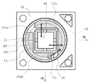
10a、10b、10c、10d、10e、10f、10g・・・絶縁層、
11、11aa、11ab、11b・・・導体配線、
12・・・熱伝導性部材、
13・・・凹部、
14・・・発光素子、
15・・・保護素子、
16・・・ワイヤ、
17・・・封止樹脂、
18・・・露出部、
19・・・支持基板、
20・・・接合層、
21・・・p型半導体層、
22・・・活性層、
23・・・n型半導体層、
24・・・n側電極、
25・・・共晶材。
Claims (5)
- 半導体発光素子と、その半導体発光素子を収容する凹部を有するパッケージと、を備え、前記パッケージを構成する絶縁性部材の内部に熱伝導性部材が埋設された半導体発光装置であって、
前記熱伝導性部材の上層および下層は前記パッケージを構成する絶縁性部材で覆われ、
前記熱伝導性部材の側面の外側に前記パッケージを構成する絶縁性部材が配置され、
前記凹部の側壁は、前記凹部を形成する最も外側の側壁と前記凹部の底面に設けられた半導体発光素子の搭載部との間に段差部を有しており、
前記熱伝導性部材は、前記搭載部の下から前記段差部の下まで延長され、
前記パッケージは前記凹部の底面に半導体発光素子を載置するための導体配線を有し、かつ、背面に前記導体配線と連続して形成される外部接続端子を有しており、
前記熱伝導性部材は前記導体配線の少なくとも一部の下方にオーバーラップして配置され、
前記外部接続端子は前記熱伝導性部材の少なくとも一部の下方にオーバーラップして配置されてなることを特徴とする半導体発光装置。 - 前記導体配線と前記熱伝導性部材との間に、前記パッケージを構成する絶縁性部材が0.1mm以下の厚みで配置されてなる請求項1に記載の半導体発光装置。
- 前記外部接続端子と前記熱伝導性部材との間にパッケージを構成する絶縁性部材が0.1mm以下の厚みで配置されてなる請求項1または2に記載の半導体発光装置。
- 前記パッケージの絶縁性部材は、セラミックスを材料として含む請求項1から3のいずれか1項に記載の半導体発光装置。
- 前記熱伝導性部材は、CuWを材料として含む請求項1から4のいずれか1項に記載の半導体発光装置。
Priority Applications (1)
| Application Number | Priority Date | Filing Date | Title |
|---|---|---|---|
| JP2008160020A JP5167977B2 (ja) | 2007-09-06 | 2008-06-19 | 半導体装置 |
Applications Claiming Priority (5)
| Application Number | Priority Date | Filing Date | Title |
|---|---|---|---|
| JP2007231385 | 2007-09-06 | ||
| JP2007231385 | 2007-09-06 | ||
| JP2008040981 | 2008-02-22 | ||
| JP2008040981 | 2008-02-22 | ||
| JP2008160020A JP5167977B2 (ja) | 2007-09-06 | 2008-06-19 | 半導体装置 |
Related Child Applications (1)
| Application Number | Title | Priority Date | Filing Date |
|---|---|---|---|
| JP2012285096A Division JP2013065891A (ja) | 2007-09-06 | 2012-12-27 | 半導体装置 |
Publications (2)
| Publication Number | Publication Date |
|---|---|
| JP2009224751A JP2009224751A (ja) | 2009-10-01 |
| JP5167977B2 true JP5167977B2 (ja) | 2013-03-21 |
Family
ID=41241187
Family Applications (3)
| Application Number | Title | Priority Date | Filing Date |
|---|---|---|---|
| JP2008160020A Active JP5167977B2 (ja) | 2007-09-06 | 2008-06-19 | 半導体装置 |
| JP2012285096A Pending JP2013065891A (ja) | 2007-09-06 | 2012-12-27 | 半導体装置 |
| JP2014188448A Pending JP2015026852A (ja) | 2007-09-06 | 2014-09-17 | 半導体装置 |
Family Applications After (2)
| Application Number | Title | Priority Date | Filing Date |
|---|---|---|---|
| JP2012285096A Pending JP2013065891A (ja) | 2007-09-06 | 2012-12-27 | 半導体装置 |
| JP2014188448A Pending JP2015026852A (ja) | 2007-09-06 | 2014-09-17 | 半導体装置 |
Country Status (1)
| Country | Link |
|---|---|
| JP (3) | JP5167977B2 (ja) |
Cited By (1)
| Publication number | Priority date | Publication date | Assignee | Title |
|---|---|---|---|---|
| US9831406B2 (en) | 2012-09-25 | 2017-11-28 | Lg Innotek Co., Ltd. | Light emitting device package |
Families Citing this family (9)
| Publication number | Priority date | Publication date | Assignee | Title |
|---|---|---|---|---|
| KR101789825B1 (ko) * | 2011-04-20 | 2017-11-20 | 엘지이노텍 주식회사 | 자외선 발광 다이오드를 이용한 발광소자 패키지 |
| JP5968674B2 (ja) | 2011-05-13 | 2016-08-10 | エルジー イノテック カンパニー リミテッド | 発光素子パッケージ及びこれを備える紫外線ランプ |
| EP3796350A1 (en) | 2011-06-07 | 2021-03-24 | FastCAP SYSTEMS Corporation | Energy storage media for ultracapacitors |
| AU2012282799A1 (en) | 2011-07-08 | 2014-02-27 | Fastcap Systems Corporation | High temperature energy storage device |
| US9558894B2 (en) | 2011-07-08 | 2017-01-31 | Fastcap Systems Corporation | Advanced electrolyte systems and their use in energy storage devices |
| US8773006B2 (en) * | 2011-08-22 | 2014-07-08 | Lg Innotek Co., Ltd. | Light emitting device package, light source module, and lighting system including the same |
| CN103078040B (zh) | 2011-08-22 | 2016-12-21 | Lg伊诺特有限公司 | 发光器件封装件和光装置 |
| JP6225453B2 (ja) * | 2012-05-24 | 2017-11-08 | 日亜化学工業株式会社 | 半導体装置 |
| JP6817599B2 (ja) * | 2016-03-10 | 2021-01-20 | パナソニックIpマネジメント株式会社 | Ledモジュール |
Family Cites Families (24)
| Publication number | Priority date | Publication date | Assignee | Title |
|---|---|---|---|---|
| JPS63181436A (ja) * | 1987-01-23 | 1988-07-26 | Matsushita Electronics Corp | 回路装置 |
| JP2911644B2 (ja) * | 1991-05-20 | 1999-06-23 | 電気化学工業株式会社 | 回路基板 |
| JPH0590967U (ja) * | 1992-05-08 | 1993-12-10 | スタンレー電気株式会社 | チップled |
| JPH08274228A (ja) * | 1995-03-29 | 1996-10-18 | Origin Electric Co Ltd | 半導体搭載基板、電力用半導体装置及び電子回路装置 |
| JPH0936433A (ja) * | 1995-07-17 | 1997-02-07 | Fuji Photo Film Co Ltd | 反射型ledを用いた光源 |
| JP4279388B2 (ja) * | 1999-01-29 | 2009-06-17 | 日亜化学工業株式会社 | 光半導体装置及びその形成方法 |
| JP3886306B2 (ja) * | 1999-10-13 | 2007-02-28 | ローム株式会社 | チップ型半導体発光装置 |
| JP3929660B2 (ja) * | 1999-10-29 | 2007-06-13 | 京セラ株式会社 | 絶縁性アルミナ質基板およびアルミナ質銅貼回路基板 |
| JP3668083B2 (ja) * | 1999-12-27 | 2005-07-06 | 京セラ株式会社 | セラミック配線基板 |
| JP4432275B2 (ja) * | 2000-07-13 | 2010-03-17 | パナソニック電工株式会社 | 光源装置 |
| US6531328B1 (en) * | 2001-10-11 | 2003-03-11 | Solidlite Corporation | Packaging of light-emitting diode |
| JP2004149401A (ja) * | 2002-09-03 | 2004-05-27 | Kyocera Corp | 接合方法および接合体 |
| JP2004207542A (ja) * | 2002-12-26 | 2004-07-22 | Kyocera Corp | 発光素子収納用パッケージおよび発光装置 |
| JP4295519B2 (ja) * | 2003-01-28 | 2009-07-15 | 京セラ株式会社 | 発光素子収納用パッケージおよび発光装置 |
| JP4501109B2 (ja) * | 2004-06-25 | 2010-07-14 | 日亜化学工業株式会社 | 発光装置 |
| JP2006093672A (ja) * | 2004-08-26 | 2006-04-06 | Toshiba Corp | 半導体発光装置 |
| JP4428372B2 (ja) * | 2004-12-13 | 2010-03-10 | ダイキン工業株式会社 | パワーモジュールおよび空気調和機 |
| JP4091063B2 (ja) * | 2005-06-07 | 2008-05-28 | 株式会社フジクラ | 発光素子実装用基板および発光素子モジュール |
| JP4839687B2 (ja) * | 2005-06-15 | 2011-12-21 | パナソニック電工株式会社 | 発光装置 |
| EP1897146A2 (en) * | 2005-06-27 | 2008-03-12 | Lamina Lighting, Inc. | Light emitting diode package and method for making same |
| JP4204058B2 (ja) * | 2005-09-20 | 2009-01-07 | パナソニック電工株式会社 | Led照明器具 |
| JP4857709B2 (ja) * | 2005-10-25 | 2012-01-18 | 日亜化学工業株式会社 | 発光装置 |
| JP4804109B2 (ja) * | 2005-10-27 | 2011-11-02 | 京セラ株式会社 | 発光素子用配線基板および発光装置並びに発光素子用配線基板の製造方法 |
| JP4940669B2 (ja) * | 2006-01-25 | 2012-05-30 | 日亜化学工業株式会社 | 半導体素子搭載用の支持体 |
-
2008
- 2008-06-19 JP JP2008160020A patent/JP5167977B2/ja active Active
-
2012
- 2012-12-27 JP JP2012285096A patent/JP2013065891A/ja active Pending
-
2014
- 2014-09-17 JP JP2014188448A patent/JP2015026852A/ja active Pending
Cited By (2)
| Publication number | Priority date | Publication date | Assignee | Title |
|---|---|---|---|---|
| US9831406B2 (en) | 2012-09-25 | 2017-11-28 | Lg Innotek Co., Ltd. | Light emitting device package |
| US9842975B2 (en) | 2012-09-25 | 2017-12-12 | Lg Innotek Co., Ltd. | Light emitting device package |
Also Published As
| Publication number | Publication date |
|---|---|
| JP2009224751A (ja) | 2009-10-01 |
| JP2013065891A (ja) | 2013-04-11 |
| JP2015026852A (ja) | 2015-02-05 |
Similar Documents
| Publication | Publication Date | Title |
|---|---|---|
| JP5167977B2 (ja) | 半導体装置 | |
| JP4780203B2 (ja) | 半導体発光装置 | |
| US10056357B2 (en) | Semiconductor light emitting device | |
| JP4325412B2 (ja) | 発光装置及び発光装置の製造方法 | |
| JP5023781B2 (ja) | 発光装置 | |
| US9246074B2 (en) | Light emitting device | |
| JP2007280983A (ja) | 発光装置 | |
| JP2022033187A (ja) | 半導体発光装置 | |
| JP5055837B2 (ja) | 発光装置 | |
| JP6191214B2 (ja) | 発光装置 | |
| JP2009272378A (ja) | 半導体装置 | |
| JP5030009B2 (ja) | 発光装置 | |
| JP5817390B2 (ja) | 発光装置 | |
| US20230155086A1 (en) | Light emitting diode package | |
| US20220209088A1 (en) | Light emitting device package | |
| JP5870582B2 (ja) | 発光装置 | |
| JP5857585B2 (ja) | 発光装置 | |
| JP5636624B2 (ja) | 発光装置 |
Legal Events
| Date | Code | Title | Description |
|---|---|---|---|
| A621 | Written request for application examination |
Free format text: JAPANESE INTERMEDIATE CODE: A621 Effective date: 20110606 |
|
| A977 | Report on retrieval |
Free format text: JAPANESE INTERMEDIATE CODE: A971007 Effective date: 20120322 |
|
| A131 | Notification of reasons for refusal |
Free format text: JAPANESE INTERMEDIATE CODE: A131 Effective date: 20120410 |
|
| A521 | Request for written amendment filed |
Free format text: JAPANESE INTERMEDIATE CODE: A523 Effective date: 20120608 |
|
| A131 | Notification of reasons for refusal |
Free format text: JAPANESE INTERMEDIATE CODE: A131 Effective date: 20120904 |
|
| A521 | Request for written amendment filed |
Free format text: JAPANESE INTERMEDIATE CODE: A523 Effective date: 20120926 |
|
| TRDD | Decision of grant or rejection written | ||
| A01 | Written decision to grant a patent or to grant a registration (utility model) |
Free format text: JAPANESE INTERMEDIATE CODE: A01 Effective date: 20121127 |
|
| A61 | First payment of annual fees (during grant procedure) |
Free format text: JAPANESE INTERMEDIATE CODE: A61 Effective date: 20121210 |
|
| R150 | Certificate of patent or registration of utility model |
Ref document number: 5167977 Country of ref document: JP Free format text: JAPANESE INTERMEDIATE CODE: R150 |
|
| FPAY | Renewal fee payment (event date is renewal date of database) |
Free format text: PAYMENT UNTIL: 20160111 Year of fee payment: 3 |
|
| R250 | Receipt of annual fees |
Free format text: JAPANESE INTERMEDIATE CODE: R250 |
|
| R250 | Receipt of annual fees |
Free format text: JAPANESE INTERMEDIATE CODE: R250 |
|
| R250 | Receipt of annual fees |
Free format text: JAPANESE INTERMEDIATE CODE: R250 |
|
| R250 | Receipt of annual fees |
Free format text: JAPANESE INTERMEDIATE CODE: R250 |
|
| R250 | Receipt of annual fees |
Free format text: JAPANESE INTERMEDIATE CODE: R250 |
|
| R250 | Receipt of annual fees |
Free format text: JAPANESE INTERMEDIATE CODE: R250 |
|
| R250 | Receipt of annual fees |
Free format text: JAPANESE INTERMEDIATE CODE: R250 |
|
| R250 | Receipt of annual fees |
Free format text: JAPANESE INTERMEDIATE CODE: R250 |
|
| R250 | Receipt of annual fees |
Free format text: JAPANESE INTERMEDIATE CODE: R250 |