JP5259368B2 - 導電性ナノファイバーシート及びその製造方法 - Google Patents
導電性ナノファイバーシート及びその製造方法 Download PDFInfo
- Publication number
- JP5259368B2 JP5259368B2 JP2008318499A JP2008318499A JP5259368B2 JP 5259368 B2 JP5259368 B2 JP 5259368B2 JP 2008318499 A JP2008318499 A JP 2008318499A JP 2008318499 A JP2008318499 A JP 2008318499A JP 5259368 B2 JP5259368 B2 JP 5259368B2
- Authority
- JP
- Japan
- Prior art keywords
- conductive
- pattern layer
- conductive pattern
- nanofiber
- layer
- Prior art date
- Legal status (The legal status is an assumption and is not a legal conclusion. Google has not performed a legal analysis and makes no representation as to the accuracy of the status listed.)
- Expired - Fee Related
Links
Images
Landscapes
- Laminated Bodies (AREA)
- Position Input By Displaying (AREA)
- Manufacture Of Switches (AREA)
- Switches That Are Operated By Magnetic Or Electric Fields (AREA)
- Contacts (AREA)
- Non-Insulated Conductors (AREA)
- Manufacturing Of Electric Cables (AREA)
Description
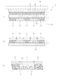
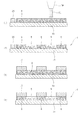
3 導電性ナノファイバー
5 絶縁パターン層
6 導電パターン層
8 タッチパネル
10 基体シート
11 エッチングレジスト層
25 位置検知マーク
33 樹脂バインダー
50 レーザー照射機の先端
51 レーザー照射光
52 保護板
53 液晶表示装置
Claims (1)
- 基体シート上に、導通可能となるように導電性ナノファイバーを含む導電パターン層を全面に形成する工程と、
前記形成された導電パターン層の一部にエネルギー線を照射して前記導電性ナノファイバーを焼き切り、前記導電性ナノファイバーを断線させて、前記導電パターン層の一部を、前記導電パターン層から絶縁した絶縁パターン層にする工程とを備えた、導電性ナノファイバーシートの製造方法。
Priority Applications (1)
| Application Number | Priority Date | Filing Date | Title |
|---|---|---|---|
| JP2008318499A JP5259368B2 (ja) | 2008-12-15 | 2008-12-15 | 導電性ナノファイバーシート及びその製造方法 |
Applications Claiming Priority (1)
| Application Number | Priority Date | Filing Date | Title |
|---|---|---|---|
| JP2008318499A JP5259368B2 (ja) | 2008-12-15 | 2008-12-15 | 導電性ナノファイバーシート及びその製造方法 |
Publications (2)
| Publication Number | Publication Date |
|---|---|
| JP2010140859A JP2010140859A (ja) | 2010-06-24 |
| JP5259368B2 true JP5259368B2 (ja) | 2013-08-07 |
Family
ID=42350800
Family Applications (1)
| Application Number | Title | Priority Date | Filing Date |
|---|---|---|---|
| JP2008318499A Expired - Fee Related JP5259368B2 (ja) | 2008-12-15 | 2008-12-15 | 導電性ナノファイバーシート及びその製造方法 |
Country Status (1)
| Country | Link |
|---|---|
| JP (1) | JP5259368B2 (ja) |
Cited By (1)
| Publication number | Priority date | Publication date | Assignee | Title |
|---|---|---|---|---|
| WO2025142439A1 (ja) * | 2023-12-28 | 2025-07-03 | 株式会社東海理化電機製作所 | 導通構造 |
Families Citing this family (60)
| Publication number | Priority date | Publication date | Assignee | Title |
|---|---|---|---|---|
| TWI426531B (zh) | 2006-10-12 | 2014-02-11 | 坎畢歐科技公司 | 以奈米線為主之透明導體及其應用 |
| JP5561714B2 (ja) * | 2009-10-13 | 2014-07-30 | 日本写真印刷株式会社 | ディスプレイ電極用透明導電膜 |
| WO2011106438A1 (en) * | 2010-02-24 | 2011-09-01 | Cambrios Technologies Corporation | Nanowire-based transparent conductors and methods of patterning same |
| TWI549900B (zh) * | 2010-03-23 | 2016-09-21 | 坎畢歐科技公司 | 奈米結構透明導體之圖案化蝕刻 |
| WO2011148429A1 (ja) * | 2010-05-28 | 2011-12-01 | 信越ポリマー株式会社 | 透明導電膜及びこれを用いた導電性基板 |
| JP5505717B2 (ja) * | 2010-06-22 | 2014-05-28 | 信越ポリマー株式会社 | 導電パターンの製造方法 |
| US8664533B2 (en) | 2010-07-05 | 2014-03-04 | Dic Corporation | Substrate having transparent conductive layer, method for producing same, transparent conductive film laminate for touch panel, and touch panel |
| KR101826379B1 (ko) * | 2010-07-09 | 2018-02-06 | 제이엔씨 주식회사 | 투명 도전성 필름 및 제조 방법 |
| JP5686405B2 (ja) * | 2010-09-24 | 2015-03-18 | 信越ポリマー株式会社 | 入力装置 |
| JP2012123744A (ja) * | 2010-12-10 | 2012-06-28 | Shin Etsu Polymer Co Ltd | 静電容量式入力装置およびその製造方法、静電容量式入力装置の入力方法 |
| JP5490033B2 (ja) * | 2011-02-07 | 2014-05-14 | 信越ポリマー株式会社 | 導電パターン形成基板の製造方法及び導電パターン形成基板 |
| JP4862969B1 (ja) * | 2011-02-07 | 2012-01-25 | ソニー株式会社 | 透明導電性素子、入力装置、電子機器および透明導電性素子作製用原盤 |
| JP5490032B2 (ja) * | 2011-02-07 | 2014-05-14 | 信越ポリマー株式会社 | 導電パターン形成基板の製造方法及び導電パターン形成基板 |
| JP5490034B2 (ja) * | 2011-02-08 | 2014-05-14 | 信越ポリマー株式会社 | 導電パターン形成基板の製造方法及び導電パターン形成基板 |
| JP2012169060A (ja) * | 2011-02-10 | 2012-09-06 | Shin Etsu Polymer Co Ltd | 導電パターン形成基板の製造方法 |
| JP5663336B2 (ja) * | 2011-02-10 | 2015-02-04 | 信越ポリマー株式会社 | 導電パターン形成基板および入力装置 |
| JP5538261B2 (ja) * | 2011-02-10 | 2014-07-02 | 信越ポリマー株式会社 | 導電パターン形成基板の製造方法 |
| JP5663337B2 (ja) * | 2011-02-14 | 2015-02-04 | 信越ポリマー株式会社 | 入力装置用配線板および入力装置 |
| KR101550481B1 (ko) * | 2011-03-30 | 2015-09-04 | 주식회사 엘지화학 | 패턴 시인성이 개선된 터치 패널, 그 제조 방법 및 이를 포함하는 디스플레이 장치 |
| JP5730240B2 (ja) | 2011-04-25 | 2015-06-03 | 信越ポリマー株式会社 | 静電容量センサシートの製造方法及び静電容量センサシート |
| JP2012238579A (ja) * | 2011-04-28 | 2012-12-06 | Fujifilm Corp | 導電性部材、その製造方法、タッチパネル及び太陽電池 |
| RU2467425C1 (ru) * | 2011-05-24 | 2012-11-20 | Открытое акционерное общество "Рязанский завод металлокерамических приборов" (ОАО "РЗМКП") | Способ изготовления геркона с контролируемыми параметрами азотируемого слоя |
| HK1201633A1 (en) | 2011-08-24 | 2015-09-04 | 宸鸿科技控股有限公司 | Patterned transparent conductors and related manufacturing methods |
| JP5386686B2 (ja) * | 2011-09-12 | 2014-01-15 | 信越ポリマー株式会社 | 透明導電膜及びその製造方法、導電性基板及びその製造方法 |
| JP2013074025A (ja) * | 2011-09-27 | 2013-04-22 | Shin Etsu Polymer Co Ltd | 導電パターン形成基板の製造方法及び導電パターン形成基板 |
| JP5646433B2 (ja) | 2011-10-31 | 2014-12-24 | 日本写真印刷株式会社 | 導電シート及びその製造方法 |
| JP2013109460A (ja) * | 2011-11-18 | 2013-06-06 | Shin Etsu Polymer Co Ltd | 透明配線シート |
| US9603242B2 (en) * | 2011-12-21 | 2017-03-21 | 3M Innovative Properties Company | Laser patterning of silver nanowire-based transparent electrically conducting coatings |
| JP5293843B2 (ja) * | 2012-01-24 | 2013-09-18 | デクセリアルズ株式会社 | 透明導電性素子、入力装置、電子機器および透明導電性素子作製用原盤 |
| JP5815439B2 (ja) * | 2012-03-02 | 2015-11-17 | 信越ポリマー株式会社 | 透明配線シート |
| JP5865851B2 (ja) * | 2012-03-23 | 2016-02-17 | 富士フイルム株式会社 | 導電性部材の製造方法、導電性部材、それを用いたタッチパネル |
| JP5952119B2 (ja) * | 2012-03-23 | 2016-07-13 | 富士フイルム株式会社 | 導電性部材およびその製造方法 |
| JP2013246885A (ja) * | 2012-05-23 | 2013-12-09 | Shin Etsu Polymer Co Ltd | 導電パターン形成シートの製造装置および導電パターン形成シートの製造方法 |
| JP5718281B2 (ja) * | 2012-05-28 | 2015-05-13 | 日本写真印刷株式会社 | 視認性と耐久性に優れた静電容量透明タッチシート |
| JP5718280B2 (ja) * | 2012-05-28 | 2015-05-13 | 日本写真印刷株式会社 | 視認性と耐久性に優れた静電容量透明タッチシート |
| JP5815473B2 (ja) * | 2012-06-04 | 2015-11-17 | 信越ポリマー株式会社 | 導電パターン形成基板の製造方法 |
| KR101310864B1 (ko) | 2012-08-22 | 2013-09-25 | (주)이엔에이치 | 메탈 나노와이어 투명 도전성 필름 및 그 제조방법 |
| US8957322B2 (en) * | 2012-12-07 | 2015-02-17 | Cambrios Technologies Corporation | Conductive films having low-visibility patterns and methods of producing the same |
| CN203250547U (zh) * | 2013-03-28 | 2013-10-23 | 南昌欧菲光科技有限公司 | 透明导电膜 |
| CN103165226B (zh) * | 2013-03-28 | 2015-04-08 | 南昌欧菲光科技有限公司 | 透明导电膜及其制备方法 |
| CN103165227B (zh) * | 2013-03-28 | 2014-09-17 | 南昌欧菲光科技有限公司 | 透明导电膜及其连通方法 |
| CN104347155A (zh) * | 2013-07-31 | 2015-02-11 | 南昌欧菲光科技有限公司 | 透明导电膜 |
| TW201520840A (zh) * | 2013-11-26 | 2015-06-01 | Henghao Technology Co Ltd | 觸控面板的形成方法 |
| JP2015128036A (ja) * | 2013-12-30 | 2015-07-09 | 日本写真印刷株式会社 | 透明導電性シート、および透明導電性シートを用いたタッチパネル |
| CN103824616B (zh) * | 2014-02-26 | 2017-01-11 | 南昌欧菲光科技有限公司 | 导电膜及其制造方法、触控元件、触控显示装置 |
| CN103871547B (zh) * | 2014-02-26 | 2017-09-29 | 南昌欧菲光科技有限公司 | 透明导电膜及含有该透明导电膜的电子装置 |
| KR101485858B1 (ko) * | 2014-03-24 | 2015-01-27 | 한국기계연구원 | 금속 나노 와이어 투명전극의 제조 방법 및 이에 의해 제조된 금속 나노 와이어 투명전극 |
| JP5825601B2 (ja) * | 2014-04-17 | 2015-12-02 | 信越ポリマー株式会社 | 入力装置 |
| JP2014167808A (ja) * | 2014-04-17 | 2014-09-11 | Shin Etsu Polymer Co Ltd | 入力装置 |
| JP5750533B2 (ja) * | 2014-04-28 | 2015-07-22 | 信越ポリマー株式会社 | 導電パターン形成基板の製造方法および導電パターン形成基板 |
| CN104851524A (zh) * | 2015-05-28 | 2015-08-19 | 京东方科技集团股份有限公司 | 透明导电薄膜的制造方法和透明导电薄膜 |
| KR102392231B1 (ko) * | 2016-12-02 | 2022-04-28 | 알프스 알파인 가부시키가이샤 | 투명 전극 부재 및 그 제조 방법, 그리고 그 투명 전극 부재를 사용한 정전 용량식 센서 |
| CN110431520B (zh) * | 2017-03-24 | 2023-05-26 | 大日本印刷株式会社 | 导电性膜、触控面板和图像显示装置 |
| JP2019008537A (ja) * | 2017-06-23 | 2019-01-17 | 株式会社東海理化電機製作所 | タッチセンサの製造方法 |
| RU2665689C1 (ru) * | 2018-01-17 | 2018-09-04 | Общество с ограниченной ответственностью ("ООО "ЭКТОН") | Способ изготовления геркона с азотированными контактными площадками |
| RU2664506C1 (ru) * | 2018-01-17 | 2018-08-20 | Общество с ограниченной ответственностью ("ООО "ЭКТОН") | Способ изготовления геркона с азотированными и наноструктурированными контактными поверхностями |
| TWI698784B (zh) * | 2018-03-14 | 2020-07-11 | 日商阿爾卑斯阿爾派股份有限公司 | 透明電極構件、層積透明電極構件及靜電電容式感測器 |
| TWI697820B (zh) | 2018-03-22 | 2020-07-01 | 日商阿爾卑斯阿爾派股份有限公司 | 透明電極構件、層積透明電極構件及靜電電容式感測器 |
| CN114242653B (zh) * | 2022-02-21 | 2022-06-03 | 威海艾迪科电子科技股份有限公司 | 一种扇出封装结构及其形成方法 |
| CN114551251B (zh) * | 2022-02-23 | 2022-09-16 | 威海艾迪科电子科技股份有限公司 | 一种具有天线结构的多芯片封装及其制备方法 |
Family Cites Families (1)
| Publication number | Priority date | Publication date | Assignee | Title |
|---|---|---|---|---|
| JP2008290354A (ja) * | 2007-05-25 | 2008-12-04 | Panasonic Corp | 導電シート及びその製造方法 |
-
2008
- 2008-12-15 JP JP2008318499A patent/JP5259368B2/ja not_active Expired - Fee Related
Cited By (1)
| Publication number | Priority date | Publication date | Assignee | Title |
|---|---|---|---|---|
| WO2025142439A1 (ja) * | 2023-12-28 | 2025-07-03 | 株式会社東海理化電機製作所 | 導通構造 |
Also Published As
| Publication number | Publication date |
|---|---|
| JP2010140859A (ja) | 2010-06-24 |
Similar Documents
| Publication | Publication Date | Title |
|---|---|---|
| JP5259368B2 (ja) | 導電性ナノファイバーシート及びその製造方法 | |
| JP5207992B2 (ja) | 導電性ナノファイバーシート及びその製造方法 | |
| US8269108B2 (en) | Transparent conductive film and conductive substrate using the same | |
| JP2010157400A (ja) | 導電性ナノファイバーシート及びその製造方法 | |
| US9253890B2 (en) | Patterned conductive film, method of fabricating the same, and application thereof | |
| CN103069369B (zh) | 输入装置 | |
| JP5561714B2 (ja) | ディスプレイ電極用透明導電膜 | |
| JP5506235B2 (ja) | 艶消し状導電性ナノファイバーシート及びその製造方法 | |
| JP6843215B2 (ja) | 透明コンダクタ、及び、透明コンダクタを製作するプロセス | |
| TW201428576A (zh) | 電極構件及包含其之觸控面板 | |
| JP2010044968A (ja) | 導電性パターン被覆体の製造方法および導電性パターン被覆体 | |
| CN104951155B (zh) | 电容式触控装置及其制作方法 | |
| CN103631459B (zh) | 触控感应层及其制造方法 | |
| WO2014175163A1 (ja) | 導電パターンの製造方法及び導電パターン形成基板 | |
| CN203930739U (zh) | 一种触控显示模组 | |
| JP2012151095A (ja) | 透明導電性フィルム、静電容量式タッチパネルの透明電極及びタッチパネル | |
| JP5335534B2 (ja) | 導電性成形品及びその製造方法 | |
| KR102008790B1 (ko) | 터치 패널 및 이의 제조방법 | |
| JP2012009506A (ja) | 導電パターンの製造方法 | |
| JP5207958B2 (ja) | 導電性ナノファイバーシート及びその製造方法 | |
| TWM453907U (zh) | 觸控面板之導電薄膜與電極層與其觸控面板 | |
| US20150059970A1 (en) | Method for making touch panel | |
| JP5386686B2 (ja) | 透明導電膜及びその製造方法、導電性基板及びその製造方法 | |
| US20150059971A1 (en) | Method for making touch panel | |
| WO2015102099A1 (ja) | 透明導電性シート、および透明導電性シートを用いたタッチパネル |
Legal Events
| Date | Code | Title | Description |
|---|---|---|---|
| A621 | Written request for application examination |
Free format text: JAPANESE INTERMEDIATE CODE: A621 Effective date: 20111026 |
|
| A977 | Report on retrieval |
Free format text: JAPANESE INTERMEDIATE CODE: A971007 Effective date: 20130212 |
|
| A131 | Notification of reasons for refusal |
Free format text: JAPANESE INTERMEDIATE CODE: A131 Effective date: 20130305 |
|
| A521 | Request for written amendment filed |
Free format text: JAPANESE INTERMEDIATE CODE: A523 Effective date: 20130328 |
|
| TRDD | Decision of grant or rejection written | ||
| A01 | Written decision to grant a patent or to grant a registration (utility model) |
Free format text: JAPANESE INTERMEDIATE CODE: A01 Effective date: 20130423 |
|
| A61 | First payment of annual fees (during grant procedure) |
Free format text: JAPANESE INTERMEDIATE CODE: A61 Effective date: 20130424 |
|
| FPAY | Renewal fee payment (event date is renewal date of database) |
Free format text: PAYMENT UNTIL: 20160502 Year of fee payment: 3 |
|
| R150 | Certificate of patent or registration of utility model |
Ref document number: 5259368 Country of ref document: JP Free format text: JAPANESE INTERMEDIATE CODE: R150 Free format text: JAPANESE INTERMEDIATE CODE: R150 |
|
| R250 | Receipt of annual fees |
Free format text: JAPANESE INTERMEDIATE CODE: R250 |
|
| R250 | Receipt of annual fees |
Free format text: JAPANESE INTERMEDIATE CODE: R250 |
|
| S533 | Written request for registration of change of name |
Free format text: JAPANESE INTERMEDIATE CODE: R313533 |
|
| R350 | Written notification of registration of transfer |
Free format text: JAPANESE INTERMEDIATE CODE: R350 |
|
| R250 | Receipt of annual fees |
Free format text: JAPANESE INTERMEDIATE CODE: R250 |
|
| R250 | Receipt of annual fees |
Free format text: JAPANESE INTERMEDIATE CODE: R250 |
|
| R250 | Receipt of annual fees |
Free format text: JAPANESE INTERMEDIATE CODE: R250 |
|
| R250 | Receipt of annual fees |
Free format text: JAPANESE INTERMEDIATE CODE: R250 |
|
| R250 | Receipt of annual fees |
Free format text: JAPANESE INTERMEDIATE CODE: R250 |
|
| R250 | Receipt of annual fees |
Free format text: JAPANESE INTERMEDIATE CODE: R250 |
|
| R250 | Receipt of annual fees |
Free format text: JAPANESE INTERMEDIATE CODE: R250 |
|
| LAPS | Cancellation because of no payment of annual fees |