JP5146256B2 - シート状構造体及びその製造方法、並びに電子機器及びその製造方法 - Google Patents
シート状構造体及びその製造方法、並びに電子機器及びその製造方法 Download PDFInfo
- Publication number
- JP5146256B2 JP5146256B2 JP2008275338A JP2008275338A JP5146256B2 JP 5146256 B2 JP5146256 B2 JP 5146256B2 JP 2008275338 A JP2008275338 A JP 2008275338A JP 2008275338 A JP2008275338 A JP 2008275338A JP 5146256 B2 JP5146256 B2 JP 5146256B2
- Authority
- JP
- Japan
- Prior art keywords
- carbon nanotube
- sheet
- coating
- film
- substrate
- Prior art date
- Legal status (The legal status is an assumption and is not a legal conclusion. Google has not performed a legal analysis and makes no representation as to the accuracy of the status listed.)
- Active
Links
Images


Classifications
-
- H—ELECTRICITY
- H01—ELECTRIC ELEMENTS
- H01L—SEMICONDUCTOR DEVICES NOT COVERED BY CLASS H10
- H01L23/00—Details of semiconductor or other solid state devices
- H01L23/34—Arrangements for cooling, heating, ventilating or temperature compensation ; Temperature sensing arrangements
- H01L23/42—Fillings or auxiliary members in containers or encapsulations selected or arranged to facilitate heating or cooling
- H01L23/433—Auxiliary members in containers characterised by their shape, e.g. pistons
-
- C—CHEMISTRY; METALLURGY
- C09—DYES; PAINTS; POLISHES; NATURAL RESINS; ADHESIVES; COMPOSITIONS NOT OTHERWISE PROVIDED FOR; APPLICATIONS OF MATERIALS NOT OTHERWISE PROVIDED FOR
- C09K—MATERIALS FOR MISCELLANEOUS APPLICATIONS, NOT PROVIDED FOR ELSEWHERE
- C09K5/00—Heat-transfer, heat-exchange or heat-storage materials, e.g. refrigerants; Materials for the production of heat or cold by chemical reactions other than by combustion
- C09K5/08—Materials not undergoing a change of physical state when used
-
- B—PERFORMING OPERATIONS; TRANSPORTING
- B82—NANOTECHNOLOGY
- B82B—NANOSTRUCTURES FORMED BY MANIPULATION OF INDIVIDUAL ATOMS, MOLECULES, OR LIMITED COLLECTIONS OF ATOMS OR MOLECULES AS DISCRETE UNITS; MANUFACTURE OR TREATMENT THEREOF
- B82B1/00—Nanostructures formed by manipulation of individual atoms or molecules, or limited collections of atoms or molecules as discrete units
-
- B—PERFORMING OPERATIONS; TRANSPORTING
- B82—NANOTECHNOLOGY
- B82B—NANOSTRUCTURES FORMED BY MANIPULATION OF INDIVIDUAL ATOMS, MOLECULES, OR LIMITED COLLECTIONS OF ATOMS OR MOLECULES AS DISCRETE UNITS; MANUFACTURE OR TREATMENT THEREOF
- B82B3/00—Manufacture or treatment of nanostructures by manipulation of individual atoms or molecules, or limited collections of atoms or molecules as discrete units
-
- H—ELECTRICITY
- H01—ELECTRIC ELEMENTS
- H01L—SEMICONDUCTOR DEVICES NOT COVERED BY CLASS H10
- H01L23/00—Details of semiconductor or other solid state devices
- H01L23/34—Arrangements for cooling, heating, ventilating or temperature compensation ; Temperature sensing arrangements
- H01L23/36—Selection of materials, or shaping, to facilitate cooling or heating, e.g. heatsinks
- H01L23/373—Cooling facilitated by selection of materials for the device or materials for thermal expansion adaptation, e.g. carbon
-
- H—ELECTRICITY
- H01—ELECTRIC ELEMENTS
- H01L—SEMICONDUCTOR DEVICES NOT COVERED BY CLASS H10
- H01L24/00—Arrangements for connecting or disconnecting semiconductor or solid-state bodies; Methods or apparatus related thereto
- H01L24/01—Means for bonding being attached to, or being formed on, the surface to be connected, e.g. chip-to-package, die-attach, "first-level" interconnects; Manufacturing methods related thereto
- H01L24/26—Layer connectors, e.g. plate connectors, solder or adhesive layers; Manufacturing methods related thereto
- H01L24/31—Structure, shape, material or disposition of the layer connectors after the connecting process
-
- H—ELECTRICITY
- H01—ELECTRIC ELEMENTS
- H01L—SEMICONDUCTOR DEVICES NOT COVERED BY CLASS H10
- H01L2224/00—Indexing scheme for arrangements for connecting or disconnecting semiconductor or solid-state bodies and methods related thereto as covered by H01L24/00
- H01L2224/01—Means for bonding being attached to, or being formed on, the surface to be connected, e.g. chip-to-package, die-attach, "first-level" interconnects; Manufacturing methods related thereto
- H01L2224/10—Bump connectors; Manufacturing methods related thereto
- H01L2224/15—Structure, shape, material or disposition of the bump connectors after the connecting process
- H01L2224/16—Structure, shape, material or disposition of the bump connectors after the connecting process of an individual bump connector
- H01L2224/161—Disposition
- H01L2224/16151—Disposition the bump connector connecting between a semiconductor or solid-state body and an item not being a semiconductor or solid-state body, e.g. chip-to-substrate, chip-to-passive
- H01L2224/16221—Disposition the bump connector connecting between a semiconductor or solid-state body and an item not being a semiconductor or solid-state body, e.g. chip-to-substrate, chip-to-passive the body and the item being stacked
- H01L2224/16225—Disposition the bump connector connecting between a semiconductor or solid-state body and an item not being a semiconductor or solid-state body, e.g. chip-to-substrate, chip-to-passive the body and the item being stacked the item being non-metallic, e.g. insulating substrate with or without metallisation
-
- H—ELECTRICITY
- H01—ELECTRIC ELEMENTS
- H01L—SEMICONDUCTOR DEVICES NOT COVERED BY CLASS H10
- H01L2224/00—Indexing scheme for arrangements for connecting or disconnecting semiconductor or solid-state bodies and methods related thereto as covered by H01L24/00
- H01L2224/01—Means for bonding being attached to, or being formed on, the surface to be connected, e.g. chip-to-package, die-attach, "first-level" interconnects; Manufacturing methods related thereto
- H01L2224/26—Layer connectors, e.g. plate connectors, solder or adhesive layers; Manufacturing methods related thereto
- H01L2224/28—Structure, shape, material or disposition of the layer connectors prior to the connecting process
- H01L2224/29—Structure, shape, material or disposition of the layer connectors prior to the connecting process of an individual layer connector
- H01L2224/29001—Core members of the layer connector
- H01L2224/29099—Material
- H01L2224/29198—Material with a principal constituent of the material being a combination of two or more materials in the form of a matrix with a filler, i.e. being a hybrid material, e.g. segmented structures, foams
- H01L2224/29298—Fillers
- H01L2224/29499—Shape or distribution of the fillers
-
- H—ELECTRICITY
- H01—ELECTRIC ELEMENTS
- H01L—SEMICONDUCTOR DEVICES NOT COVERED BY CLASS H10
- H01L2224/00—Indexing scheme for arrangements for connecting or disconnecting semiconductor or solid-state bodies and methods related thereto as covered by H01L24/00
- H01L2224/01—Means for bonding being attached to, or being formed on, the surface to be connected, e.g. chip-to-package, die-attach, "first-level" interconnects; Manufacturing methods related thereto
- H01L2224/26—Layer connectors, e.g. plate connectors, solder or adhesive layers; Manufacturing methods related thereto
- H01L2224/31—Structure, shape, material or disposition of the layer connectors after the connecting process
- H01L2224/32—Structure, shape, material or disposition of the layer connectors after the connecting process of an individual layer connector
- H01L2224/321—Disposition
- H01L2224/32151—Disposition the layer connector connecting between a semiconductor or solid-state body and an item not being a semiconductor or solid-state body, e.g. chip-to-substrate, chip-to-passive
- H01L2224/32221—Disposition the layer connector connecting between a semiconductor or solid-state body and an item not being a semiconductor or solid-state body, e.g. chip-to-substrate, chip-to-passive the body and the item being stacked
- H01L2224/32225—Disposition the layer connector connecting between a semiconductor or solid-state body and an item not being a semiconductor or solid-state body, e.g. chip-to-substrate, chip-to-passive the body and the item being stacked the item being non-metallic, e.g. insulating substrate with or without metallisation
-
- H—ELECTRICITY
- H01—ELECTRIC ELEMENTS
- H01L—SEMICONDUCTOR DEVICES NOT COVERED BY CLASS H10
- H01L2224/00—Indexing scheme for arrangements for connecting or disconnecting semiconductor or solid-state bodies and methods related thereto as covered by H01L24/00
- H01L2224/73—Means for bonding being of different types provided for in two or more of groups H01L2224/10, H01L2224/18, H01L2224/26, H01L2224/34, H01L2224/42, H01L2224/50, H01L2224/63, H01L2224/71
- H01L2224/732—Location after the connecting process
- H01L2224/73201—Location after the connecting process on the same surface
- H01L2224/73203—Bump and layer connectors
- H01L2224/73204—Bump and layer connectors the bump connector being embedded into the layer connector
-
- H—ELECTRICITY
- H01—ELECTRIC ELEMENTS
- H01L—SEMICONDUCTOR DEVICES NOT COVERED BY CLASS H10
- H01L2224/00—Indexing scheme for arrangements for connecting or disconnecting semiconductor or solid-state bodies and methods related thereto as covered by H01L24/00
- H01L2224/73—Means for bonding being of different types provided for in two or more of groups H01L2224/10, H01L2224/18, H01L2224/26, H01L2224/34, H01L2224/42, H01L2224/50, H01L2224/63, H01L2224/71
- H01L2224/732—Location after the connecting process
- H01L2224/73251—Location after the connecting process on different surfaces
- H01L2224/73253—Bump and layer connectors
-
- H—ELECTRICITY
- H01—ELECTRIC ELEMENTS
- H01L—SEMICONDUCTOR DEVICES NOT COVERED BY CLASS H10
- H01L23/00—Details of semiconductor or other solid state devices
- H01L23/34—Arrangements for cooling, heating, ventilating or temperature compensation ; Temperature sensing arrangements
- H01L23/36—Selection of materials, or shaping, to facilitate cooling or heating, e.g. heatsinks
- H01L23/373—Cooling facilitated by selection of materials for the device or materials for thermal expansion adaptation, e.g. carbon
- H01L23/3733—Cooling facilitated by selection of materials for the device or materials for thermal expansion adaptation, e.g. carbon having a heterogeneous or anisotropic structure, e.g. powder or fibres in a matrix, wire mesh, porous structures
-
- H—ELECTRICITY
- H01—ELECTRIC ELEMENTS
- H01L—SEMICONDUCTOR DEVICES NOT COVERED BY CLASS H10
- H01L2924/00—Indexing scheme for arrangements or methods for connecting or disconnecting semiconductor or solid-state bodies as covered by H01L24/00
- H01L2924/01—Chemical elements
- H01L2924/01005—Boron [B]
-
- H—ELECTRICITY
- H01—ELECTRIC ELEMENTS
- H01L—SEMICONDUCTOR DEVICES NOT COVERED BY CLASS H10
- H01L2924/00—Indexing scheme for arrangements or methods for connecting or disconnecting semiconductor or solid-state bodies as covered by H01L24/00
- H01L2924/01—Chemical elements
- H01L2924/01006—Carbon [C]
-
- H—ELECTRICITY
- H01—ELECTRIC ELEMENTS
- H01L—SEMICONDUCTOR DEVICES NOT COVERED BY CLASS H10
- H01L2924/00—Indexing scheme for arrangements or methods for connecting or disconnecting semiconductor or solid-state bodies as covered by H01L24/00
- H01L2924/01—Chemical elements
- H01L2924/01013—Aluminum [Al]
-
- H—ELECTRICITY
- H01—ELECTRIC ELEMENTS
- H01L—SEMICONDUCTOR DEVICES NOT COVERED BY CLASS H10
- H01L2924/00—Indexing scheme for arrangements or methods for connecting or disconnecting semiconductor or solid-state bodies as covered by H01L24/00
- H01L2924/01—Chemical elements
- H01L2924/01018—Argon [Ar]
-
- H—ELECTRICITY
- H01—ELECTRIC ELEMENTS
- H01L—SEMICONDUCTOR DEVICES NOT COVERED BY CLASS H10
- H01L2924/00—Indexing scheme for arrangements or methods for connecting or disconnecting semiconductor or solid-state bodies as covered by H01L24/00
- H01L2924/01—Chemical elements
- H01L2924/01019—Potassium [K]
-
- H—ELECTRICITY
- H01—ELECTRIC ELEMENTS
- H01L—SEMICONDUCTOR DEVICES NOT COVERED BY CLASS H10
- H01L2924/00—Indexing scheme for arrangements or methods for connecting or disconnecting semiconductor or solid-state bodies as covered by H01L24/00
- H01L2924/01—Chemical elements
- H01L2924/01023—Vanadium [V]
-
- H—ELECTRICITY
- H01—ELECTRIC ELEMENTS
- H01L—SEMICONDUCTOR DEVICES NOT COVERED BY CLASS H10
- H01L2924/00—Indexing scheme for arrangements or methods for connecting or disconnecting semiconductor or solid-state bodies as covered by H01L24/00
- H01L2924/01—Chemical elements
- H01L2924/01027—Cobalt [Co]
-
- H—ELECTRICITY
- H01—ELECTRIC ELEMENTS
- H01L—SEMICONDUCTOR DEVICES NOT COVERED BY CLASS H10
- H01L2924/00—Indexing scheme for arrangements or methods for connecting or disconnecting semiconductor or solid-state bodies as covered by H01L24/00
- H01L2924/01—Chemical elements
- H01L2924/01029—Copper [Cu]
-
- H—ELECTRICITY
- H01—ELECTRIC ELEMENTS
- H01L—SEMICONDUCTOR DEVICES NOT COVERED BY CLASS H10
- H01L2924/00—Indexing scheme for arrangements or methods for connecting or disconnecting semiconductor or solid-state bodies as covered by H01L24/00
- H01L2924/01—Chemical elements
- H01L2924/01033—Arsenic [As]
-
- H—ELECTRICITY
- H01—ELECTRIC ELEMENTS
- H01L—SEMICONDUCTOR DEVICES NOT COVERED BY CLASS H10
- H01L2924/00—Indexing scheme for arrangements or methods for connecting or disconnecting semiconductor or solid-state bodies as covered by H01L24/00
- H01L2924/01—Chemical elements
- H01L2924/0104—Zirconium [Zr]
-
- H—ELECTRICITY
- H01—ELECTRIC ELEMENTS
- H01L—SEMICONDUCTOR DEVICES NOT COVERED BY CLASS H10
- H01L2924/00—Indexing scheme for arrangements or methods for connecting or disconnecting semiconductor or solid-state bodies as covered by H01L24/00
- H01L2924/01—Chemical elements
- H01L2924/01041—Niobium [Nb]
-
- H—ELECTRICITY
- H01—ELECTRIC ELEMENTS
- H01L—SEMICONDUCTOR DEVICES NOT COVERED BY CLASS H10
- H01L2924/00—Indexing scheme for arrangements or methods for connecting or disconnecting semiconductor or solid-state bodies as covered by H01L24/00
- H01L2924/01—Chemical elements
- H01L2924/01042—Molybdenum [Mo]
-
- H—ELECTRICITY
- H01—ELECTRIC ELEMENTS
- H01L—SEMICONDUCTOR DEVICES NOT COVERED BY CLASS H10
- H01L2924/00—Indexing scheme for arrangements or methods for connecting or disconnecting semiconductor or solid-state bodies as covered by H01L24/00
- H01L2924/01—Chemical elements
- H01L2924/01046—Palladium [Pd]
-
- H—ELECTRICITY
- H01—ELECTRIC ELEMENTS
- H01L—SEMICONDUCTOR DEVICES NOT COVERED BY CLASS H10
- H01L2924/00—Indexing scheme for arrangements or methods for connecting or disconnecting semiconductor or solid-state bodies as covered by H01L24/00
- H01L2924/01—Chemical elements
- H01L2924/01047—Silver [Ag]
-
- H—ELECTRICITY
- H01—ELECTRIC ELEMENTS
- H01L—SEMICONDUCTOR DEVICES NOT COVERED BY CLASS H10
- H01L2924/00—Indexing scheme for arrangements or methods for connecting or disconnecting semiconductor or solid-state bodies as covered by H01L24/00
- H01L2924/01—Chemical elements
- H01L2924/01049—Indium [In]
-
- H—ELECTRICITY
- H01—ELECTRIC ELEMENTS
- H01L—SEMICONDUCTOR DEVICES NOT COVERED BY CLASS H10
- H01L2924/00—Indexing scheme for arrangements or methods for connecting or disconnecting semiconductor or solid-state bodies as covered by H01L24/00
- H01L2924/01—Chemical elements
- H01L2924/0105—Tin [Sn]
-
- H—ELECTRICITY
- H01—ELECTRIC ELEMENTS
- H01L—SEMICONDUCTOR DEVICES NOT COVERED BY CLASS H10
- H01L2924/00—Indexing scheme for arrangements or methods for connecting or disconnecting semiconductor or solid-state bodies as covered by H01L24/00
- H01L2924/01—Chemical elements
- H01L2924/01072—Hafnium [Hf]
-
- H—ELECTRICITY
- H01—ELECTRIC ELEMENTS
- H01L—SEMICONDUCTOR DEVICES NOT COVERED BY CLASS H10
- H01L2924/00—Indexing scheme for arrangements or methods for connecting or disconnecting semiconductor or solid-state bodies as covered by H01L24/00
- H01L2924/01—Chemical elements
- H01L2924/01073—Tantalum [Ta]
-
- H—ELECTRICITY
- H01—ELECTRIC ELEMENTS
- H01L—SEMICONDUCTOR DEVICES NOT COVERED BY CLASS H10
- H01L2924/00—Indexing scheme for arrangements or methods for connecting or disconnecting semiconductor or solid-state bodies as covered by H01L24/00
- H01L2924/01—Chemical elements
- H01L2924/01074—Tungsten [W]
-
- H—ELECTRICITY
- H01—ELECTRIC ELEMENTS
- H01L—SEMICONDUCTOR DEVICES NOT COVERED BY CLASS H10
- H01L2924/00—Indexing scheme for arrangements or methods for connecting or disconnecting semiconductor or solid-state bodies as covered by H01L24/00
- H01L2924/01—Chemical elements
- H01L2924/01078—Platinum [Pt]
-
- H—ELECTRICITY
- H01—ELECTRIC ELEMENTS
- H01L—SEMICONDUCTOR DEVICES NOT COVERED BY CLASS H10
- H01L2924/00—Indexing scheme for arrangements or methods for connecting or disconnecting semiconductor or solid-state bodies as covered by H01L24/00
- H01L2924/01—Chemical elements
- H01L2924/01079—Gold [Au]
-
- H—ELECTRICITY
- H01—ELECTRIC ELEMENTS
- H01L—SEMICONDUCTOR DEVICES NOT COVERED BY CLASS H10
- H01L2924/00—Indexing scheme for arrangements or methods for connecting or disconnecting semiconductor or solid-state bodies as covered by H01L24/00
- H01L2924/049—Nitrides composed of metals from groups of the periodic table
- H01L2924/0494—4th Group
- H01L2924/04941—TiN
-
- H—ELECTRICITY
- H01—ELECTRIC ELEMENTS
- H01L—SEMICONDUCTOR DEVICES NOT COVERED BY CLASS H10
- H01L2924/00—Indexing scheme for arrangements or methods for connecting or disconnecting semiconductor or solid-state bodies as covered by H01L24/00
- H01L2924/049—Nitrides composed of metals from groups of the periodic table
- H01L2924/0495—5th Group
- H01L2924/04953—TaN
-
- H—ELECTRICITY
- H01—ELECTRIC ELEMENTS
- H01L—SEMICONDUCTOR DEVICES NOT COVERED BY CLASS H10
- H01L2924/00—Indexing scheme for arrangements or methods for connecting or disconnecting semiconductor or solid-state bodies as covered by H01L24/00
- H01L2924/15—Details of package parts other than the semiconductor or other solid state devices to be connected
- H01L2924/151—Die mounting substrate
- H01L2924/156—Material
- H01L2924/15786—Material with a principal constituent of the material being a non metallic, non metalloid inorganic material
- H01L2924/15788—Glasses, e.g. amorphous oxides, nitrides or fluorides
-
- H—ELECTRICITY
- H01—ELECTRIC ELEMENTS
- H01L—SEMICONDUCTOR DEVICES NOT COVERED BY CLASS H10
- H01L2924/00—Indexing scheme for arrangements or methods for connecting or disconnecting semiconductor or solid-state bodies as covered by H01L24/00
- H01L2924/15—Details of package parts other than the semiconductor or other solid state devices to be connected
- H01L2924/161—Cap
- H01L2924/1615—Shape
- H01L2924/16152—Cap comprising a cavity for hosting the device, e.g. U-shaped cap
-
- Y—GENERAL TAGGING OF NEW TECHNOLOGICAL DEVELOPMENTS; GENERAL TAGGING OF CROSS-SECTIONAL TECHNOLOGIES SPANNING OVER SEVERAL SECTIONS OF THE IPC; TECHNICAL SUBJECTS COVERED BY FORMER USPC CROSS-REFERENCE ART COLLECTIONS [XRACs] AND DIGESTS
- Y10—TECHNICAL SUBJECTS COVERED BY FORMER USPC
- Y10T—TECHNICAL SUBJECTS COVERED BY FORMER US CLASSIFICATION
- Y10T428/00—Stock material or miscellaneous articles
- Y10T428/30—Self-sustaining carbon mass or layer with impregnant or other layer
Description
第1実施形態によるカーボンナノチューブシート及びその製造方法について図1乃至図7を用いて説明する。
第2実施形態によるカーボンナノチューブシートの製造方法について図8及び図9を用いて説明する。図1乃至図7に示す第1実施形態によるカーボンナノチューブシート及びその製造方法と同様の構成要素には同一の符号を付し、説明を省略し或いは簡潔にする。
第3実施形態によるカーボンナノチューブシート及びその製造方法について図10及び図11を用いて説明する。図1乃至図9に示す第1及び第2実施形態によるカーボンナノチューブシート及びその製造方法と同様の構成要素には同一の符号を付し、説明を省略し或いは簡潔にする。
第4実施形態によるカーボンナノチューブシート及びその製造方法について図12を用いて説明する。図1乃至図11に示す第1乃至第3実施形態によるカーボンナノチューブシート及びその製造方法と同様の構成要素には同一の符号を付し、説明を省略し或いは簡潔にする。
第5実施形態によるカーボンナノチューブシート及びその製造方法について図13乃至図15を用いて説明する。図1乃至図12に示す第1乃至第4実施形態によるカーボンナノチューブシート及びその製造方法と同様の構成要素には同一の符号を付し、説明を省略し或いは簡潔にする。
第6実施形態によるカーボンナノチューブシート及びその製造方法について図16乃至図19を用いて説明する。図1乃至図15に示す第1乃至第5実施形態によるカーボンナノチューブシート及びその製造方法と同様の構成要素には同一の符号を付し、説明を省略し或いは簡潔にする。
本発明の第7実施形態による電子機器について図20を用いて説明する。
本発明の第8実施形態による電子機器について図21を用いて説明する。
本発明の第9実施形態による電子機器について図22を用いて説明する。
上記実施形態に限らず種々の変形が可能である。
複数の前記線状構造体の間隙に充填され、複数の前記線状構造体を保持する充填層と、
複数の前記線状構造体の少なくとも一方の端部に形成され、前記充填層の構成材料よりも熱伝導率の高い材料よりなる第1の被膜と
を有することを特徴とするシート状構造体。
前記第1の被膜は、隣接する前記線状構造体を互いに結合する
ことを特徴とするシート状構造体。
複数の前記線状構造体の少なくとも一方の端部に形成され、0.1W/m・K以上の熱伝導率を有し、隣接する前記線状構造体を互いに結合する第1の被膜と
を有することを特徴とするシート状構造体。
前記第1の被膜と前記線状構造体との間に形成されたグラファイト層を更に有する
ことを特徴とするシート状構造体。
複数の前記線状構造体の他方の端部に形成された第2の被膜を更に有する
ことを特徴とするシート状構造体。
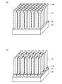
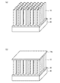
複数の前記線状構造体は、互いに第1の間隔をもって配置され、互いに前記第1の間隔よりも大きな第2の間隔をもって配置された複数の線状構造体束を形成している
ことを特徴とするシート状構造体。
複数の前記線状構造体は、シートの膜厚方向に配向している
ことを特徴とするシート状構造体。
複数の前記線状構造体のそれぞれは、シートの膜厚方向に対して傾いており、隣接する前記線状構造体が互いに接触している
ことを特徴とするシート状構造体。
前記第2の被膜は、0.1W/m・K以上の熱伝導率を有する
ことを特徴とするシート状構造体。
前記発熱部により生じた熱を放熱する放熱部と、
前記発熱部と前記放熱部との間に配置され、複数の炭素元素の線状構造体と、複数の前記線状構造体の少なくとも一方の端部に形成された被膜とを有するシート状構造体と
を有することを特徴とする電子機器。
前記シート状構造体は、複数の前記線状構造体の間隙に充填され、複数の前記線状構造体を保持する充填層を更に有する
ことを特徴とする電子機器。
前記被膜は、隣接する前記線状構造体を互いに結合するように形成されており、
複数の前記線状構造体は、前記被膜により保持されている
ことを特徴とする電子機器。
前記触媒金属膜を触媒として、前記第1の基板上に、複数の炭素元素の線状構造体を成長する工程と、
複数の前記線状構造体の端部上に、第1の被膜を形成する工程と、
前記第1の被膜上に第2の基板を貼り合わせた後、複数の前記線状構造体と前記第1の基板との界面から前記第1の基板を剥離する工程と、
前記線状構造体間に充填材を充填し、充填層を形成する工程と、
前記第2の基板を除去する工程と
を有することを特徴とするシート状構造体の製造方法。
前記第1の基板を剥離した後、
前記第1の基板を剥離することにより露出した複数の前記線状構造体の端部上に、第2の被膜を形成する工程を更に有する
ことを特徴とするシート状構造体の製造方法。
前記触媒金属膜を触媒として、前記基板上に、複数の炭素元素の線状構造体を成長する工程と、
複数の前記線状構造体の端部上に、隣接する前記線状構造体を互いに結合するように、第1の被膜を形成する工程と、
複数の前記線状構造体と前記基板との界面から前記基板を剥離する工程と、
を有することを特徴とするシート状構造体の製造方法。
前記基板を剥離した後、
前記基板を剥離することにより露出した複数の前記線状構造体の端部上に、第2の被膜を形成する工程を更に有する
ことを特徴とするシート状構造体の製造方法。
複数の前記線状構造体を成長する工程では、端部がグラファイト層により覆われた前記線状構造体を成長する
ことを特徴とするシート状構造体の製造方法。
前記被膜の融点よりも高い温度で熱処理を行い、前記被膜をリフローする工程と
を有することを特徴とする電子機器の製造方法。
前記シート状構造体は、複数の前記線状構造体の間隙に充填され、複数の前記線状構造体を保持する充填層を更に有する
ことを特徴とする電子機器の製造方法。
前記被膜は、隣接する前記線状構造体を互いに結合するように形成されており、
複数の前記線状構造体は、前記被膜により保持されている
ことを特徴とする電子機器の製造方法。
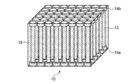
12…カーボンナノチューブ
14…被膜
16…充填層
20…グラファイト層
22…カーボンナノチューブ束
30,40…基板
42…接着材層
44…犠牲層
46…熱圧着層
50…ステージ
52…加圧ヘッド
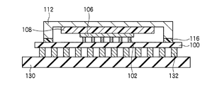
100…回路基板
102,132…はんだバンプ
104…アンダーフィル
106…半導体素子
108,112,126…カーボンナノチューブシート
110…ヒートスプレッダ
114,124…ヒートシンク
120…高出力増幅器
122…パッケージ
130…プリント配線基板
Claims (7)
- 複数の炭素元素の線状構造体と、
複数の前記線状構造体の間隙に充填され、複数の前記線状構造体を保持する充填層と、
複数の前記線状構造体の少なくとも一方の端部に形成され、前記充填層の構成材料よりも熱伝導率の高い材料よりなる第1の被膜と、
前記第1の被膜と前記線状構造体との間に形成されたグラファイト層と
を有することを特徴とするシート状構造体。 - 請求項1記載のシート状構造体において、
前記第1の被膜は、隣接する前記線状構造体を互いに結合する
ことを特徴とするシート状構造体。 - 請求項1又は2記載のシート状構造体において、
複数の前記線状構造体の他方の端部に形成された第2の被膜を更に有する
ことを特徴とするシート状構造体。 - 請求項1乃至3のいずれか1項に記載のシート状構造体において、
複数の前記線状構造体のそれぞれは、シートの膜厚方向に対して傾いており、隣接する前記線状構造体が互いに接触している
ことを特徴とするシート状構造体。 - 発熱部と、
前記発熱部により生じた熱を放熱する放熱部と、
前記発熱部と前記放熱部との間に配置され、複数の炭素元素の線状構造体と、複数の前記線状構造体の少なくとも一方の端部に形成された被膜と、前記被膜と前記線状構造体との間に形成されたグラファイト層とを有するシート状構造体と
を有することを特徴とする電子機器。 - 第1の基板上に、触媒金属膜を形成する工程と、
前記触媒金属膜を触媒として、前記第1の基板上に、端部がグラファイト層により覆われた複数の炭素元素の線状構造体を成長する工程と、
前記グラファイト層により覆われた複数の前記線状構造体の端部上に、第1の被膜を形成する工程と、
前記第1の被膜上に第2の基板を貼り合わせた後、複数の前記線状構造体と前記第1の基板との界面から前記第1の基板を剥離する工程と、
前記線状構造体間に充填材を充填し、充填層を形成する工程と、
前記第2の基板を除去する工程と
を有することを特徴とするシート状構造体の製造方法。 - 発熱部と、前記発熱部により生じた熱を放熱する放熱部とを、複数の炭素元素の線状構造体と、複数の前記線状構造体の少なくとも一方の端部に形成された被膜と、前記被膜と前記線状構造体との間に形成されたグラファイト層とを有するシート状構造体を介して接合する工程と、
前記被膜の融点よりも高い温度で熱処理を行い、前記被膜をリフローする工程と
を有することを特徴とする電子機器の製造方法。
Priority Applications (6)
| Application Number | Priority Date | Filing Date | Title |
|---|---|---|---|
| JP2008275338A JP5146256B2 (ja) | 2008-03-18 | 2008-10-27 | シート状構造体及びその製造方法、並びに電子機器及びその製造方法 |
| KR1020090021322A KR101051351B1 (ko) | 2008-03-18 | 2009-03-12 | 시트 형상 구조체와 그 제조 방법, 및 전자 기기와 그 제조방법 |
| TW098108570A TWI398508B (zh) | 2008-03-18 | 2009-03-17 | 片狀結構及製造片狀結構之方法 |
| US12/405,578 US8749979B2 (en) | 2008-03-18 | 2009-03-17 | Sheet structure and method of manufacturing sheet structure |
| CN2009101280244A CN101540302B (zh) | 2008-03-18 | 2009-03-17 | 片结构和制造片结构的方法 |
| EP09155530.0A EP2104141B1 (en) | 2008-03-18 | 2009-03-18 | Sheet structure and method of manufacturing sheet structure |
Applications Claiming Priority (3)
| Application Number | Priority Date | Filing Date | Title |
|---|---|---|---|
| JP2008068992 | 2008-03-18 | ||
| JP2008068992 | 2008-03-18 | ||
| JP2008275338A JP5146256B2 (ja) | 2008-03-18 | 2008-10-27 | シート状構造体及びその製造方法、並びに電子機器及びその製造方法 |
Related Child Applications (1)
| Application Number | Title | Priority Date | Filing Date |
|---|---|---|---|
| JP2012201242A Division JP5768786B2 (ja) | 2008-03-18 | 2012-09-13 | シート状構造体及び電子機器 |
Publications (2)
| Publication Number | Publication Date |
|---|---|
| JP2009260238A JP2009260238A (ja) | 2009-11-05 |
| JP5146256B2 true JP5146256B2 (ja) | 2013-02-20 |
Family
ID=40651768
Family Applications (1)
| Application Number | Title | Priority Date | Filing Date |
|---|---|---|---|
| JP2008275338A Active JP5146256B2 (ja) | 2008-03-18 | 2008-10-27 | シート状構造体及びその製造方法、並びに電子機器及びその製造方法 |
Country Status (6)
| Country | Link |
|---|---|
| US (1) | US8749979B2 (ja) |
| EP (1) | EP2104141B1 (ja) |
| JP (1) | JP5146256B2 (ja) |
| KR (1) | KR101051351B1 (ja) |
| CN (1) | CN101540302B (ja) |
| TW (1) | TWI398508B (ja) |
Families Citing this family (67)
| Publication number | Priority date | Publication date | Assignee | Title |
|---|---|---|---|---|
| EP1885652A4 (en) * | 2005-05-03 | 2010-02-24 | Nanocomp Technologies Inc | CARBON MATERIALS AND METHOD OF MANUFACTURING THEREFOR |
| JP4864093B2 (ja) | 2005-07-28 | 2012-01-25 | ナノコンプ テクノロジーズ インコーポレイテッド | ナノ繊維質材料の形成および収穫に関するシステムおよび方法 |
| JP5595737B2 (ja) * | 2007-02-27 | 2014-09-24 | ナノコンプ テクノロジーズ インコーポレイテッド | 熱保護材料およびその製造方法 |
| US9061913B2 (en) | 2007-06-15 | 2015-06-23 | Nanocomp Technologies, Inc. | Injector apparatus and methods for production of nanostructures |
| US8246886B2 (en) * | 2007-07-09 | 2012-08-21 | Nanocomp Technologies, Inc. | Chemically-assisted alignment of nanotubes within extensible structures |
| CA2695853A1 (en) * | 2007-08-07 | 2009-02-12 | Nanocomp Technologies, Inc. | Electrically and thermally non-metallic conductive nanostructure-based adapters |
| US20090044848A1 (en) * | 2007-08-14 | 2009-02-19 | Nanocomp Technologies, Inc. | Nanostructured Material-Based Thermoelectric Generators |
| CA2723619A1 (en) | 2008-05-07 | 2009-11-12 | Nanocomp Technologies, Inc. | Nanostructure-based heating devices and method of use |
| WO2009137722A1 (en) * | 2008-05-07 | 2009-11-12 | Nanocomp Technologies, Inc. | Carbon nanotube-based coaxial electrical cables and wiring harness |
| US8304291B2 (en) * | 2009-06-29 | 2012-11-06 | Advanced Micro Devices, Inc. | Semiconductor chip thermal interface structures |
| US8405996B2 (en) * | 2009-06-30 | 2013-03-26 | General Electric Company | Article including thermal interface element and method of preparation |
| US8354593B2 (en) * | 2009-07-10 | 2013-01-15 | Nanocomp Technologies, Inc. | Hybrid conductors and method of making same |
| US8106510B2 (en) | 2009-08-04 | 2012-01-31 | Raytheon Company | Nano-tube thermal interface structure |
| KR101007057B1 (ko) * | 2009-10-08 | 2011-01-12 | 동국대학교 산학협력단 | 나노구조를 갖는 mim 캐패시터 제조방법 |
| JP5356972B2 (ja) * | 2009-10-20 | 2013-12-04 | 新光電気工業株式会社 | 放熱用部品及びその製造方法、半導体パッケージ |
| CN101747869A (zh) * | 2009-12-18 | 2010-06-23 | 东南大学 | 热界面材料 |
| CN102107546B (zh) * | 2009-12-29 | 2013-04-24 | 北京富纳特创新科技有限公司 | 汽车玻璃贴膜及汽车 |
| WO2011111112A1 (ja) * | 2010-03-12 | 2011-09-15 | 富士通株式会社 | 放熱構造体およびその製造方法 |
| JP5447069B2 (ja) * | 2010-03-24 | 2014-03-19 | 富士通株式会社 | シート状構造体、電子機器及び電子機器の製造方法 |
| JP5447117B2 (ja) * | 2010-04-09 | 2014-03-19 | 富士通株式会社 | 電子機器の製造方法 |
| KR101050198B1 (ko) | 2010-07-26 | 2011-07-19 | 연세대학교 산학협력단 | 나노선 다이오드 생성 방법 |
| WO2012094398A1 (en) * | 2011-01-04 | 2012-07-12 | Nanocomp Technologies, Inc. | Nanotube-based insulators |
| JP5714928B2 (ja) * | 2011-02-09 | 2015-05-07 | 日東電工株式会社 | 繊維状柱状構造体集合体および放熱部材 |
| EP2763167B1 (en) * | 2011-09-26 | 2016-06-29 | Fujitsu Limited | Heat-dissipating material and method for producing same, and electronic device and method for producing same |
| JP5788760B2 (ja) * | 2011-10-19 | 2015-10-07 | 日東電工株式会社 | 熱伝導性シート、led実装用基板およびledモジュール |
| JP5935302B2 (ja) * | 2011-11-18 | 2016-06-15 | 富士通株式会社 | シート状構造体及びその製造方法並びに電子機器及びその製造方法 |
| CN103178027B (zh) * | 2011-12-21 | 2016-03-09 | 清华大学 | 散热结构及应用该散热结构的电子设备 |
| FR2985603B1 (fr) * | 2012-01-10 | 2016-12-23 | Commissariat Energie Atomique | Dispositif de gestion thermique passif |
| JP5998557B2 (ja) * | 2012-03-23 | 2016-09-28 | 富士通株式会社 | 放熱シートの製造方法 |
| FR2995877B1 (fr) * | 2012-09-21 | 2014-10-24 | Thales Sa | Structure meca-thermique adaptee pour un environnement spatial |
| JP6118540B2 (ja) * | 2012-11-08 | 2017-04-19 | 新光電気工業株式会社 | 放熱部品及びその製造方法 |
| US20140151009A1 (en) * | 2012-11-30 | 2014-06-05 | General Electric Company | Thermal interface element and method of preparation |
| WO2014109014A1 (ja) * | 2013-01-09 | 2014-07-17 | 株式会社日立製作所 | 半導体装置およびその製造方法 |
| JP6115270B2 (ja) * | 2013-04-09 | 2017-04-19 | 富士通株式会社 | 放熱構造体及びその製造方法並びに電子装置 |
| WO2014196006A1 (ja) * | 2013-06-03 | 2014-12-11 | 富士通株式会社 | 放熱構造体及びその製造方法並びに電子装置 |
| WO2014204561A1 (en) | 2013-06-17 | 2014-12-24 | Nanocomp Technologies, Inc. | Exfoliating-dispersing agents for nanotubes, bundles and fibers |
| JP6186933B2 (ja) * | 2013-06-21 | 2017-08-30 | 富士通株式会社 | 接合シート及びその製造方法、並びに放熱機構及びその製造方法 |
| CN103367275B (zh) * | 2013-07-10 | 2016-10-05 | 华为技术有限公司 | 一种界面导热片及其制备方法、散热系统 |
| WO2015045648A1 (ja) * | 2013-09-30 | 2015-04-02 | 富士電機株式会社 | 半導体装置、半導体装置の組み立て方法、半導体装置用部品及び単位モジュール |
| US9905658B2 (en) * | 2013-11-26 | 2018-02-27 | Nxp Usa, Inc. | Transistors with field plates resistant to field plate material migration and methods of their fabrication |
| US10839975B2 (en) | 2014-03-10 | 2020-11-17 | The Boeing Company | Graphene coated electronic components |
| US9930808B2 (en) * | 2014-03-10 | 2018-03-27 | The Boeing Company | Graphene-based thermal management systems |
| JP6223903B2 (ja) * | 2014-04-30 | 2017-11-01 | 新光電気工業株式会社 | カーボンナノチューブシート及び電子機器とカーボンナノチューブシートの製造方法及び電子機器の製造方法 |
| US9482477B2 (en) * | 2014-07-28 | 2016-11-01 | Northrop Grumman Systems Corporation | Nano-thermal agents for enhanced interfacial thermal conductance |
| JP6295238B2 (ja) | 2014-10-31 | 2018-03-14 | デクセリアルズ株式会社 | 熱伝導シート、熱伝導シートの製造方法、放熱部材及び半導体装置 |
| JP6821575B2 (ja) | 2015-02-03 | 2021-01-27 | ナノコンプ テクノロジーズ,インク. | カーボンナノチューブ構造体およびその生成のための方法 |
| US9468989B2 (en) | 2015-02-26 | 2016-10-18 | Northrop Grumman Systems Corporation | High-conductivity bonding of metal nanowire arrays |
| FR3041274B1 (fr) * | 2015-09-17 | 2017-09-29 | Commissariat Energie Atomique | Procede d'orientation d'objets allonges disposes en surface d'un substrat |
| JP6582854B2 (ja) * | 2015-10-14 | 2019-10-02 | 富士通株式会社 | 放熱シート、放熱シートの製造方法、及び電子装置 |
| JP6301978B2 (ja) * | 2016-01-26 | 2018-03-28 | デクセリアルズ株式会社 | 熱伝導シート、熱伝導シートの製造方法、放熱部材及び半導体装置 |
| US10304803B2 (en) * | 2016-05-05 | 2019-05-28 | Invensas Corporation | Nanoscale interconnect array for stacked dies |
| CN109075152B (zh) | 2016-05-06 | 2023-01-24 | 斯莫特克有限公司 | 组装平台 |
| JP2019532497A (ja) * | 2016-08-30 | 2019-11-07 | テラダイオード, インコーポレーテッド | カーボンナノチューブを利用した高出力レーザパッケージング |
| US10153224B2 (en) * | 2016-09-14 | 2018-12-11 | Globalfoundries Inc. | Backside spacer structures for improved thermal performance |
| DE102016217735A1 (de) * | 2016-09-16 | 2018-03-22 | Carl Zeiss Smt Gmbh | Komponente für eine Spiegelanordnung für die EUV-Lithographie |
| JP6810343B2 (ja) * | 2016-10-17 | 2021-01-06 | 富士通株式会社 | カーボンナノチューブ構造、放熱シート及びカーボンナノチューブ構造の製造方法 |
| US10581082B2 (en) | 2016-11-15 | 2020-03-03 | Nanocomp Technologies, Inc. | Systems and methods for making structures defined by CNT pulp networks |
| CN108251063B (zh) * | 2016-12-28 | 2021-05-11 | 有研工程技术研究院有限公司 | 一种高性能复合相变材料及其制备方法 |
| US11279836B2 (en) | 2017-01-09 | 2022-03-22 | Nanocomp Technologies, Inc. | Intumescent nanostructured materials and methods of manufacturing same |
| JP6901896B2 (ja) * | 2017-03-31 | 2021-07-14 | 日立造船株式会社 | フィラー・樹脂複合体、フィラー・樹脂複合体の製造方法、フィラー・樹脂複合層、および、フィラー・樹脂複合体の使用方法 |
| CN109152279A (zh) * | 2017-06-27 | 2019-01-04 | 卓英社有限公司 | 导热部件 |
| CN111128637B (zh) | 2018-11-01 | 2021-02-26 | 清华大学 | 场发射体的制备方法 |
| CN111115615B (zh) | 2018-11-01 | 2021-08-31 | 清华大学 | 碳纳米管阵列的转移方法 |
| CN111121981B (zh) | 2018-11-01 | 2021-04-02 | 清华大学 | 黑体辐射源的制备方法 |
| CN110003438A (zh) * | 2019-03-29 | 2019-07-12 | 傲川科技(河源)有限公司 | 导热凝胶及其制备方法 |
| KR102584991B1 (ko) * | 2019-06-14 | 2023-10-05 | 삼성전기주식회사 | 반도체 패키지 |
| CN110625877B (zh) * | 2019-09-05 | 2021-06-08 | 上海阿莱德实业股份有限公司 | 一种导热界面材料的制备方法 |
Family Cites Families (28)
| Publication number | Priority date | Publication date | Assignee | Title |
|---|---|---|---|---|
| JPS5313610A (en) * | 1976-07-23 | 1978-02-07 | Nippon Carbon Co Ltd | Compound sheet materials |
| WO1995002313A1 (en) * | 1993-07-06 | 1995-01-19 | Kabushiki Kaisha Toshiba | Heat dissipating sheet |
| US6630772B1 (en) | 1998-09-21 | 2003-10-07 | Agere Systems Inc. | Device comprising carbon nanotube field emitter structure and process for forming device |
| GB0008897D0 (en) * | 2000-04-12 | 2000-05-31 | Cheiros Technology Ltd | Improvements relating to heat transfer |
| JP2002141633A (ja) | 2000-10-25 | 2002-05-17 | Lucent Technol Inc | 垂直にナノ相互接続された回路デバイスからなる製品及びその製造方法 |
| US6821625B2 (en) * | 2001-09-27 | 2004-11-23 | International Business Machines Corporation | Thermal spreader using thermal conduits |
| US6965513B2 (en) * | 2001-12-20 | 2005-11-15 | Intel Corporation | Carbon nanotube thermal interface structures |
| US6837273B2 (en) * | 2002-06-19 | 2005-01-04 | Saint-Gobain Technical Fabrics Canada, Ltd. | Inversion liner and liner components for conduits |
| US7095053B2 (en) * | 2003-05-05 | 2006-08-22 | Lamina Ceramics, Inc. | Light emitting diodes packaged for high temperature operation |
| US7112472B2 (en) * | 2003-06-25 | 2006-09-26 | Intel Corporation | Methods of fabricating a composite carbon nanotube thermal interface device |
| US7168484B2 (en) * | 2003-06-30 | 2007-01-30 | Intel Corporation | Thermal interface apparatus, systems, and methods |
| US7077858B2 (en) * | 2003-09-22 | 2006-07-18 | Coolhead Technologies, Inc. | Flexible heat exchangers for medical cooling and warming applications |
| JP4412052B2 (ja) | 2003-10-28 | 2010-02-10 | 富士ゼロックス株式会社 | 複合材およびその製造方法 |
| JP2005150362A (ja) | 2003-11-14 | 2005-06-09 | Dainippon Printing Co Ltd | 高熱伝導性シートおよびその製造方法 |
| US7279916B2 (en) * | 2004-10-05 | 2007-10-09 | Nanoconduction, Inc. | Apparatus and test device for the application and measurement of prescribed, predicted and controlled contact pressure on wires |
| JP2006147801A (ja) | 2004-11-18 | 2006-06-08 | Seiko Precision Inc | 放熱シート、インターフェース、電子部品及び放熱シートの製造方法 |
| CN100337981C (zh) | 2005-03-24 | 2007-09-19 | 清华大学 | 热界面材料及其制造方法 |
| US20060231946A1 (en) * | 2005-04-14 | 2006-10-19 | Molecular Nanosystems, Inc. | Nanotube surface coatings for improved wettability |
| CN100404242C (zh) * | 2005-04-14 | 2008-07-23 | 清华大学 | 热界面材料及其制造方法 |
| JP2006303240A (ja) | 2005-04-21 | 2006-11-02 | Fujikura Ltd | 放熱シート、放熱体、放熱シート製造方法及び伝熱方法 |
| CN100454526C (zh) * | 2005-06-30 | 2009-01-21 | 鸿富锦精密工业(深圳)有限公司 | 热界面材料制造方法 |
| CN1891780B (zh) * | 2005-07-01 | 2013-04-24 | 清华大学 | 热界面材料及其制备方法 |
| JP4684053B2 (ja) | 2005-09-09 | 2011-05-18 | 株式会社アルバック | カーボンナノチューブの作製方法及びその固定方法 |
| US7505275B2 (en) * | 2005-11-04 | 2009-03-17 | Graftech International Holdings Inc. | LED with integral via |
| WO2007110899A1 (ja) | 2006-03-24 | 2007-10-04 | Fujitsu Limited | 炭素系繊維のデバイス構造およびその製造方法 |
| CN101054467B (zh) * | 2006-04-14 | 2010-05-26 | 清华大学 | 碳纳米管复合材料及其制备方法 |
| JP2008034474A (ja) | 2006-07-26 | 2008-02-14 | Sharp Corp | 伝熱シート及び基板装置 |
| US7742673B2 (en) * | 2007-09-28 | 2010-06-22 | General Electric Company | Thermal mangement article having thermal wave guide |
-
2008
- 2008-10-27 JP JP2008275338A patent/JP5146256B2/ja active Active
-
2009
- 2009-03-12 KR KR1020090021322A patent/KR101051351B1/ko active IP Right Grant
- 2009-03-17 CN CN2009101280244A patent/CN101540302B/zh active Active
- 2009-03-17 US US12/405,578 patent/US8749979B2/en active Active
- 2009-03-17 TW TW098108570A patent/TWI398508B/zh active
- 2009-03-18 EP EP09155530.0A patent/EP2104141B1/en active Active
Also Published As
| Publication number | Publication date |
|---|---|
| CN101540302B (zh) | 2012-04-04 |
| EP2104141A2 (en) | 2009-09-23 |
| EP2104141A3 (en) | 2010-10-27 |
| KR20090100257A (ko) | 2009-09-23 |
| US20090237886A1 (en) | 2009-09-24 |
| JP2009260238A (ja) | 2009-11-05 |
| EP2104141B1 (en) | 2016-05-18 |
| US8749979B2 (en) | 2014-06-10 |
| CN101540302A (zh) | 2009-09-23 |
| KR101051351B1 (ko) | 2011-07-22 |
| TWI398508B (zh) | 2013-06-11 |
| TW200951210A (en) | 2009-12-16 |
Similar Documents
| Publication | Publication Date | Title |
|---|---|---|
| JP5146256B2 (ja) | シート状構造体及びその製造方法、並びに電子機器及びその製造方法 | |
| JP5104688B2 (ja) | シート状構造体及びその製造方法並びに電子機器 | |
| JP6132768B2 (ja) | 放熱材料及びその製造方法 | |
| JP5506657B2 (ja) | シート状構造体、半導体装置及び炭素構造体の成長方法 | |
| JP5239768B2 (ja) | 放熱材料並びに電子機器及びその製造方法 | |
| JP6127417B2 (ja) | 放熱材料の製造方法 | |
| JP5790023B2 (ja) | 電子部品の製造方法 | |
| JP5013116B2 (ja) | シート状構造体及びその製造方法並びに電子機器 | |
| JP2011204749A (ja) | シート状構造体、電子機器及び電子機器の製造方法 | |
| JP5447117B2 (ja) | 電子機器の製造方法 | |
| JP2013115094A (ja) | 放熱材料及びその製造方法 | |
| JP5343620B2 (ja) | 放熱材料及びその製造方法並びに電子機器及びその製造方法 | |
| EP2061077B1 (en) | Sheet structure and method of manufacturing the same | |
| JP2011035046A (ja) | シート状構造体及びその製造方法 | |
| JP5760668B2 (ja) | シート状構造体及びその製造方法並びに電子機器及びその製造方法 | |
| JP5768786B2 (ja) | シート状構造体及び電子機器 | |
| JP6223903B2 (ja) | カーボンナノチューブシート及び電子機器とカーボンナノチューブシートの製造方法及び電子機器の製造方法 | |
| JP5786986B2 (ja) | 炭素構造体の成長方法及びシート状構造体の製造方法 | |
| JP2013232683A (ja) | シート状構造体及びその製造方法 | |
| JP2013110217A (ja) | シート状構造体及びその製造方法並びに電子機器及びその製造方法 |
Legal Events
| Date | Code | Title | Description |
|---|---|---|---|
| A621 | Written request for application examination |
Free format text: JAPANESE INTERMEDIATE CODE: A621 Effective date: 20110808 |
|
| A977 | Report on retrieval |
Free format text: JAPANESE INTERMEDIATE CODE: A971007 Effective date: 20120706 |
|
| A131 | Notification of reasons for refusal |
Free format text: JAPANESE INTERMEDIATE CODE: A131 Effective date: 20120717 |
|
| A521 | Request for written amendment filed |
Free format text: JAPANESE INTERMEDIATE CODE: A523 Effective date: 20120913 |
|
| TRDD | Decision of grant or rejection written | ||
| A01 | Written decision to grant a patent or to grant a registration (utility model) |
Free format text: JAPANESE INTERMEDIATE CODE: A01 Effective date: 20121030 |
|
| A61 | First payment of annual fees (during grant procedure) |
Free format text: JAPANESE INTERMEDIATE CODE: A61 Effective date: 20121112 |
|
| R150 | Certificate of patent or registration of utility model |
Ref document number: 5146256 Country of ref document: JP Free format text: JAPANESE INTERMEDIATE CODE: R150 Free format text: JAPANESE INTERMEDIATE CODE: R150 |
|
| FPAY | Renewal fee payment (event date is renewal date of database) |
Free format text: PAYMENT UNTIL: 20151207 Year of fee payment: 3 |