JP5026848B2 - 光半導体デバイスおよびその製造方法 - Google Patents
光半導体デバイスおよびその製造方法 Download PDFInfo
- Publication number
- JP5026848B2 JP5026848B2 JP2007110057A JP2007110057A JP5026848B2 JP 5026848 B2 JP5026848 B2 JP 5026848B2 JP 2007110057 A JP2007110057 A JP 2007110057A JP 2007110057 A JP2007110057 A JP 2007110057A JP 5026848 B2 JP5026848 B2 JP 5026848B2
- Authority
- JP
- Japan
- Prior art keywords
- lead
- optical semiconductor
- semiconductor device
- semiconductor chip
- holder
- Prior art date
- Legal status (The legal status is an assumption and is not a legal conclusion. Google has not performed a legal analysis and makes no representation as to the accuracy of the status listed.)
- Expired - Fee Related
Links
- 230000003287 optical effect Effects 0.000 title claims abstract description 156
- 239000004065 semiconductor Substances 0.000 title claims abstract description 155
- 238000004519 manufacturing process Methods 0.000 title claims description 16
- 238000007789 sealing Methods 0.000 claims abstract description 24
- 238000005520 cutting process Methods 0.000 claims description 24
- 229920005989 resin Polymers 0.000 claims description 19
- 239000011347 resin Substances 0.000 claims description 19
- 238000007689 inspection Methods 0.000 claims description 9
- 239000003566 sealing material Substances 0.000 claims description 8
- 238000009751 slip forming Methods 0.000 claims description 2
- 230000035939 shock Effects 0.000 abstract description 10
- PCHJSUWPFVWCPO-UHFFFAOYSA-N gold Chemical compound [Au] PCHJSUWPFVWCPO-UHFFFAOYSA-N 0.000 abstract description 9
- 238000005452 bending Methods 0.000 description 25
- 230000000694 effects Effects 0.000 description 9
- 229910000679 solder Inorganic materials 0.000 description 7
- 238000010586 diagram Methods 0.000 description 6
- 238000000034 method Methods 0.000 description 6
- 238000001953 recrystallisation Methods 0.000 description 5
- 230000008901 benefit Effects 0.000 description 4
- 238000006073 displacement reaction Methods 0.000 description 4
- 238000000465 moulding Methods 0.000 description 4
- 235000014676 Phragmites communis Nutrition 0.000 description 3
- 239000000853 adhesive Substances 0.000 description 3
- 238000000605 extraction Methods 0.000 description 3
- 238000002347 injection Methods 0.000 description 3
- 239000007924 injection Substances 0.000 description 3
- 230000007246 mechanism Effects 0.000 description 3
- 230000008569 process Effects 0.000 description 3
- 239000000758 substrate Substances 0.000 description 3
- 239000004954 Polyphthalamide Substances 0.000 description 2
- 230000008859 change Effects 0.000 description 2
- 238000005304 joining Methods 0.000 description 2
- 239000000463 material Substances 0.000 description 2
- 239000002184 metal Substances 0.000 description 2
- 229910052751 metal Inorganic materials 0.000 description 2
- 229920006375 polyphtalamide Polymers 0.000 description 2
- 230000009467 reduction Effects 0.000 description 2
- 238000000926 separation method Methods 0.000 description 2
- XUIMIQQOPSSXEZ-UHFFFAOYSA-N Silicon Chemical compound [Si] XUIMIQQOPSSXEZ-UHFFFAOYSA-N 0.000 description 1
- 230000001070 adhesive effect Effects 0.000 description 1
- 238000000149 argon plasma sintering Methods 0.000 description 1
- 230000008602 contraction Effects 0.000 description 1
- 230000017525 heat dissipation Effects 0.000 description 1
- 230000006872 improvement Effects 0.000 description 1
- 230000000704 physical effect Effects 0.000 description 1
- 238000003825 pressing Methods 0.000 description 1
- 230000000630 rising effect Effects 0.000 description 1
- 229910052710 silicon Inorganic materials 0.000 description 1
- 239000010703 silicon Substances 0.000 description 1
- 230000007306 turnover Effects 0.000 description 1
- 238000003466 welding Methods 0.000 description 1
Images


Classifications
-
- H—ELECTRICITY
- H01—ELECTRIC ELEMENTS
- H01L—SEMICONDUCTOR DEVICES NOT COVERED BY CLASS H10
- H01L33/00—Semiconductor devices with at least one potential-jump barrier or surface barrier specially adapted for light emission; Processes or apparatus specially adapted for the manufacture or treatment thereof or of parts thereof; Details thereof
- H01L33/48—Semiconductor devices with at least one potential-jump barrier or surface barrier specially adapted for light emission; Processes or apparatus specially adapted for the manufacture or treatment thereof or of parts thereof; Details thereof characterised by the semiconductor body packages
- H01L33/62—Arrangements for conducting electric current to or from the semiconductor body, e.g. lead-frames, wire-bonds or solder balls
-
- H—ELECTRICITY
- H01—ELECTRIC ELEMENTS
- H01L—SEMICONDUCTOR DEVICES NOT COVERED BY CLASS H10
- H01L31/00—Semiconductor devices sensitive to infrared radiation, light, electromagnetic radiation of shorter wavelength or corpuscular radiation and specially adapted either for the conversion of the energy of such radiation into electrical energy or for the control of electrical energy by such radiation; Processes or apparatus specially adapted for the manufacture or treatment thereof or of parts thereof; Details thereof
- H01L31/02—Details
- H01L31/02016—Circuit arrangements of general character for the devices
- H01L31/02019—Circuit arrangements of general character for the devices for devices characterised by at least one potential jump barrier or surface barrier
-
- H—ELECTRICITY
- H01—ELECTRIC ELEMENTS
- H01L—SEMICONDUCTOR DEVICES NOT COVERED BY CLASS H10
- H01L31/00—Semiconductor devices sensitive to infrared radiation, light, electromagnetic radiation of shorter wavelength or corpuscular radiation and specially adapted either for the conversion of the energy of such radiation into electrical energy or for the control of electrical energy by such radiation; Processes or apparatus specially adapted for the manufacture or treatment thereof or of parts thereof; Details thereof
- H01L31/02—Details
- H01L31/0203—Containers; Encapsulations, e.g. encapsulation of photodiodes
-
- H—ELECTRICITY
- H01—ELECTRIC ELEMENTS
- H01L—SEMICONDUCTOR DEVICES NOT COVERED BY CLASS H10
- H01L31/00—Semiconductor devices sensitive to infrared radiation, light, electromagnetic radiation of shorter wavelength or corpuscular radiation and specially adapted either for the conversion of the energy of such radiation into electrical energy or for the control of electrical energy by such radiation; Processes or apparatus specially adapted for the manufacture or treatment thereof or of parts thereof; Details thereof
- H01L31/18—Processes or apparatus specially adapted for the manufacture or treatment of these devices or of parts thereof
-
- H—ELECTRICITY
- H01—ELECTRIC ELEMENTS
- H01L—SEMICONDUCTOR DEVICES NOT COVERED BY CLASS H10
- H01L2224/00—Indexing scheme for arrangements for connecting or disconnecting semiconductor or solid-state bodies and methods related thereto as covered by H01L24/00
- H01L2224/01—Means for bonding being attached to, or being formed on, the surface to be connected, e.g. chip-to-package, die-attach, "first-level" interconnects; Manufacturing methods related thereto
- H01L2224/02—Bonding areas; Manufacturing methods related thereto
- H01L2224/04—Structure, shape, material or disposition of the bonding areas prior to the connecting process
- H01L2224/05—Structure, shape, material or disposition of the bonding areas prior to the connecting process of an individual bonding area
- H01L2224/0554—External layer
- H01L2224/05599—Material
-
- H—ELECTRICITY
- H01—ELECTRIC ELEMENTS
- H01L—SEMICONDUCTOR DEVICES NOT COVERED BY CLASS H10
- H01L2224/00—Indexing scheme for arrangements for connecting or disconnecting semiconductor or solid-state bodies and methods related thereto as covered by H01L24/00
- H01L2224/01—Means for bonding being attached to, or being formed on, the surface to be connected, e.g. chip-to-package, die-attach, "first-level" interconnects; Manufacturing methods related thereto
- H01L2224/42—Wire connectors; Manufacturing methods related thereto
- H01L2224/44—Structure, shape, material or disposition of the wire connectors prior to the connecting process
- H01L2224/45—Structure, shape, material or disposition of the wire connectors prior to the connecting process of an individual wire connector
- H01L2224/45001—Core members of the connector
- H01L2224/45099—Material
- H01L2224/451—Material with a principal constituent of the material being a metal or a metalloid, e.g. boron (B), silicon (Si), germanium (Ge), arsenic (As), antimony (Sb), tellurium (Te) and polonium (Po), and alloys thereof
- H01L2224/45138—Material with a principal constituent of the material being a metal or a metalloid, e.g. boron (B), silicon (Si), germanium (Ge), arsenic (As), antimony (Sb), tellurium (Te) and polonium (Po), and alloys thereof the principal constituent melting at a temperature of greater than or equal to 950°C and less than 1550°C
- H01L2224/45144—Gold (Au) as principal constituent
-
- H—ELECTRICITY
- H01—ELECTRIC ELEMENTS
- H01L—SEMICONDUCTOR DEVICES NOT COVERED BY CLASS H10
- H01L2224/00—Indexing scheme for arrangements for connecting or disconnecting semiconductor or solid-state bodies and methods related thereto as covered by H01L24/00
- H01L2224/01—Means for bonding being attached to, or being formed on, the surface to be connected, e.g. chip-to-package, die-attach, "first-level" interconnects; Manufacturing methods related thereto
- H01L2224/42—Wire connectors; Manufacturing methods related thereto
- H01L2224/47—Structure, shape, material or disposition of the wire connectors after the connecting process
- H01L2224/48—Structure, shape, material or disposition of the wire connectors after the connecting process of an individual wire connector
- H01L2224/4805—Shape
- H01L2224/4809—Loop shape
- H01L2224/48091—Arched
-
- H—ELECTRICITY
- H01—ELECTRIC ELEMENTS
- H01L—SEMICONDUCTOR DEVICES NOT COVERED BY CLASS H10
- H01L2224/00—Indexing scheme for arrangements for connecting or disconnecting semiconductor or solid-state bodies and methods related thereto as covered by H01L24/00
- H01L2224/01—Means for bonding being attached to, or being formed on, the surface to be connected, e.g. chip-to-package, die-attach, "first-level" interconnects; Manufacturing methods related thereto
- H01L2224/42—Wire connectors; Manufacturing methods related thereto
- H01L2224/47—Structure, shape, material or disposition of the wire connectors after the connecting process
- H01L2224/48—Structure, shape, material or disposition of the wire connectors after the connecting process of an individual wire connector
- H01L2224/481—Disposition
- H01L2224/48151—Connecting between a semiconductor or solid-state body and an item not being a semiconductor or solid-state body, e.g. chip-to-substrate, chip-to-passive
- H01L2224/48221—Connecting between a semiconductor or solid-state body and an item not being a semiconductor or solid-state body, e.g. chip-to-substrate, chip-to-passive the body and the item being stacked
- H01L2224/48245—Connecting between a semiconductor or solid-state body and an item not being a semiconductor or solid-state body, e.g. chip-to-substrate, chip-to-passive the body and the item being stacked the item being metallic
- H01L2224/48247—Connecting between a semiconductor or solid-state body and an item not being a semiconductor or solid-state body, e.g. chip-to-substrate, chip-to-passive the body and the item being stacked the item being metallic connecting the wire to a bond pad of the item
-
- H—ELECTRICITY
- H01—ELECTRIC ELEMENTS
- H01L—SEMICONDUCTOR DEVICES NOT COVERED BY CLASS H10
- H01L2224/00—Indexing scheme for arrangements for connecting or disconnecting semiconductor or solid-state bodies and methods related thereto as covered by H01L24/00
- H01L2224/01—Means for bonding being attached to, or being formed on, the surface to be connected, e.g. chip-to-package, die-attach, "first-level" interconnects; Manufacturing methods related thereto
- H01L2224/42—Wire connectors; Manufacturing methods related thereto
- H01L2224/47—Structure, shape, material or disposition of the wire connectors after the connecting process
- H01L2224/48—Structure, shape, material or disposition of the wire connectors after the connecting process of an individual wire connector
- H01L2224/484—Connecting portions
- H01L2224/48463—Connecting portions the connecting portion on the bonding area of the semiconductor or solid-state body being a ball bond
- H01L2224/48464—Connecting portions the connecting portion on the bonding area of the semiconductor or solid-state body being a ball bond the other connecting portion not on the bonding area also being a ball bond, i.e. ball-to-ball
-
- H—ELECTRICITY
- H01—ELECTRIC ELEMENTS
- H01L—SEMICONDUCTOR DEVICES NOT COVERED BY CLASS H10
- H01L2224/00—Indexing scheme for arrangements for connecting or disconnecting semiconductor or solid-state bodies and methods related thereto as covered by H01L24/00
- H01L2224/01—Means for bonding being attached to, or being formed on, the surface to be connected, e.g. chip-to-package, die-attach, "first-level" interconnects; Manufacturing methods related thereto
- H01L2224/42—Wire connectors; Manufacturing methods related thereto
- H01L2224/47—Structure, shape, material or disposition of the wire connectors after the connecting process
- H01L2224/48—Structure, shape, material or disposition of the wire connectors after the connecting process of an individual wire connector
- H01L2224/484—Connecting portions
- H01L2224/48463—Connecting portions the connecting portion on the bonding area of the semiconductor or solid-state body being a ball bond
- H01L2224/48465—Connecting portions the connecting portion on the bonding area of the semiconductor or solid-state body being a ball bond the other connecting portion not on the bonding area being a wedge bond, i.e. ball-to-wedge, regular stitch
-
- H—ELECTRICITY
- H01—ELECTRIC ELEMENTS
- H01L—SEMICONDUCTOR DEVICES NOT COVERED BY CLASS H10
- H01L2224/00—Indexing scheme for arrangements for connecting or disconnecting semiconductor or solid-state bodies and methods related thereto as covered by H01L24/00
- H01L2224/80—Methods for connecting semiconductor or other solid state bodies using means for bonding being attached to, or being formed on, the surface to be connected
- H01L2224/85—Methods for connecting semiconductor or other solid state bodies using means for bonding being attached to, or being formed on, the surface to be connected using a wire connector
- H01L2224/8538—Bonding interfaces outside the semiconductor or solid-state body
- H01L2224/85399—Material
-
- H—ELECTRICITY
- H01—ELECTRIC ELEMENTS
- H01L—SEMICONDUCTOR DEVICES NOT COVERED BY CLASS H10
- H01L24/00—Arrangements for connecting or disconnecting semiconductor or solid-state bodies; Methods or apparatus related thereto
- H01L24/01—Means for bonding being attached to, or being formed on, the surface to be connected, e.g. chip-to-package, die-attach, "first-level" interconnects; Manufacturing methods related thereto
- H01L24/42—Wire connectors; Manufacturing methods related thereto
- H01L24/44—Structure, shape, material or disposition of the wire connectors prior to the connecting process
- H01L24/45—Structure, shape, material or disposition of the wire connectors prior to the connecting process of an individual wire connector
-
- H—ELECTRICITY
- H01—ELECTRIC ELEMENTS
- H01L—SEMICONDUCTOR DEVICES NOT COVERED BY CLASS H10
- H01L24/00—Arrangements for connecting or disconnecting semiconductor or solid-state bodies; Methods or apparatus related thereto
- H01L24/01—Means for bonding being attached to, or being formed on, the surface to be connected, e.g. chip-to-package, die-attach, "first-level" interconnects; Manufacturing methods related thereto
- H01L24/42—Wire connectors; Manufacturing methods related thereto
- H01L24/47—Structure, shape, material or disposition of the wire connectors after the connecting process
- H01L24/48—Structure, shape, material or disposition of the wire connectors after the connecting process of an individual wire connector
-
- H—ELECTRICITY
- H01—ELECTRIC ELEMENTS
- H01L—SEMICONDUCTOR DEVICES NOT COVERED BY CLASS H10
- H01L2924/00—Indexing scheme for arrangements or methods for connecting or disconnecting semiconductor or solid-state bodies as covered by H01L24/00
- H01L2924/0001—Technical content checked by a classifier
- H01L2924/00014—Technical content checked by a classifier the subject-matter covered by the group, the symbol of which is combined with the symbol of this group, being disclosed without further technical details
-
- H—ELECTRICITY
- H01—ELECTRIC ELEMENTS
- H01L—SEMICONDUCTOR DEVICES NOT COVERED BY CLASS H10
- H01L2924/00—Indexing scheme for arrangements or methods for connecting or disconnecting semiconductor or solid-state bodies as covered by H01L24/00
- H01L2924/10—Details of semiconductor or other solid state devices to be connected
- H01L2924/11—Device type
- H01L2924/12—Passive devices, e.g. 2 terminal devices
- H01L2924/1204—Optical Diode
- H01L2924/12041—LED
-
- H—ELECTRICITY
- H01—ELECTRIC ELEMENTS
- H01L—SEMICONDUCTOR DEVICES NOT COVERED BY CLASS H10
- H01L2924/00—Indexing scheme for arrangements or methods for connecting or disconnecting semiconductor or solid-state bodies as covered by H01L24/00
- H01L2924/10—Details of semiconductor or other solid state devices to be connected
- H01L2924/11—Device type
- H01L2924/12—Passive devices, e.g. 2 terminal devices
- H01L2924/1204—Optical Diode
- H01L2924/12043—Photo diode
Description
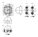
前記光半導体チップを収容するホルダー部と、
前記光半導体チップが配置されるマウント部を有し、前記ホルダー部の第1の側面と該第1の側面とは反対の側の第2の側面との2つの側面から導出される第1のリードと、
前記光半導体チップから延びるワイヤの接合部を有し、前記ホルダー部の前記第1の側面の第1のリードが導出される位置とは異なる位置から導出される第2のリードと、
前記ホルダー部の前記第2の側面の第1のリードが導出される位置とは異なる位置から導出される第3のリードと、
を有し、
前記第3のリードの一方の端部は、前記ホルダー部の内側に存在する前記第2のリードの一方の端部と対向して配置されており、
前記第3のリードは、電極としての機能を有さない保持部材である
ことを特徴とする光半導体デバイスである。
前記第1のリード部の両端、前記第2のリード部、前記第3のリード部を支持するホルダー部を成形する工程と、
前記マウント部上に光半導体チップを載置する工程と、
光半導体チップと前記接合部とをワイヤにより接合する工程と、を順に行い、
次いで、
前記リードフレームの前記ホルダー部の内側において、前記第3のリード部と前記第2のリード部との前記連結部を切断して、電極としての機能を有さない保持部材として機能する第3のリード部を形成する工程と、
前記第1のリード部と残りのリードフレームとの間に電圧を印加して製品検査を行う工程と、
前記ホルダー部内における、前記第1のリード、前記第2のリード、前記第3のリード、および光半導体チップを封止材料で覆う工程と、
を有することを特徴とする光半導体デバイスの製造方法である。
前記光半導体チップ2を収容するホルダー部6と、
前記光半導体チップ2が配置されるマウント部を有し、前記ホルダー部6の第1の側面と該第1の側面とは反対の側の第2の側面との2つの側面から導出される第1のリード3と、
前記光半導体チップ2から延びる導電性のワイヤ5の接合部を有し、前記ホルダー部6の前記第1の側面の第1のリード3が導出される位置とは異なる位置から導出される第2のリード4aと、
前記ホルダー部6の前記第2の側面の第1のリード3が導出される位置とは異なる位置から導出される第3のリード4bと、
前記ホルダー部6内における、前記第1のリード3、前記第2のリード4a、前記第3のリード4b、および光半導体チップ2を覆う封止部8と、を有している光半導体デバイスである。
前記第1のリード部3の両端、前記第2のリード部4a、前記第3のリード部4bを支持するホルダー部6を成形する工程と、
前記リードフレーム50の前記ホルダー部6の内側において、前記第3のリード部4bと前記第2のリード部4aとの前記連結部を切断する工程と、
前記マウント部上に光半導体チップ2を載置する工程と、
光半導体チップ2と前記第2のリード部4aの前記接合部とを導電性のワイヤ5により接合する工程と、
前記ホルダー部6内における、前記第1のリード3、前記第2のリード4a、前記第3のリード4b、および光半導体チップ2を封止材料で覆う工程と、
によって、光半導体デバイスを製造することができる。
前記第1のリード部3の両端、前記第2のリード部4a、前記第3のリード部4bを支持するホルダー部6を成形する工程と、
前記リードフレーム50の前記ホルダー部6の内側において、前記第1のリード部3と前記第2のリード部4aとの前記連結部を切断する工程と、
前記マウント部上に光半導体チップ2を載置する工程と、
光半導体チップ2と前記第2のリード部4aの前記接合部とを導電性のワイヤ5により接合する工程と、
前記ホルダー部6内における、前記第1のリード3、前記第2のリード4a、前記第3のリード4b、および光半導体チップ2を封止材料で覆う工程と、
によって、光半導体デバイスを製造することができる。
3 第1のリード
4 第2のリード
4a,4b 第2のリードの片
5 ワイヤ
6 ホルダー部
7 レンズ部
8 封止材
50 リードフレーム
Claims (8)
- 光半導体チップと、
前記光半導体チップを収容するホルダー部と、
前記光半導体チップが配置されるマウント部を有し、前記ホルダー部の第1の側面と該第1の側面とは反対の側の第2の側面との2つの側面から導出される第1のリードと、
前記光半導体チップから延びるワイヤの接合部を有し、前記ホルダー部の前記第1の側面の第1のリードが導出される位置とは異なる位置から導出される第2のリードと、
前記ホルダー部の前記第2の側面の第1のリードが導出される位置とは異なる位置から導出される第3のリードと、
を有し、
前記第3のリードの一方の端部は、前記ホルダー部の内側に存在する前記第2のリードの一方の端部と対向して配置されており、
前記第3のリードは、電極としての機能を有さない保持部材である
ことを特徴とする光半導体デバイス。 - 請求項1記載の光半導体デバイスにおいて、前記ホルダー部内における、前記第1のリード、前記第2のリード、前記第3のリード、および光半導体チップを覆う封止部をさらに有していることを特徴とする光半導体デバイス。
- 請求項1記載の光半導体デバイスにおいて、前記ホルダー部の内側に位置する前記第2のリードの一方の端部および前記第3のリードの一方の端部の少なくともいずれかは、屈曲形状を有していることを特徴とする光半導体デバイス。
- 請求項3記載の光半導体デバイスにおいて、前記屈曲形状は、2箇所の曲げ部と、第1リードの延出方向に平行な端部とから構成されていることを特徴とする光半導体デバイス。
- 請求項1乃至請求項4のいずれか一項に記載の光半導体デバイスにおいて、前記第1のリード、前記第2のリード、前記第3のリードは、それぞれ前記ホルダー部から平行に延出していることを特徴とする光半導体デバイス。
- 請求項1乃至請求項5のいずれか一項に記載の光半導体デバイスにおいて、前記光半導体チップと前記ワイヤとの接続部、前記第2リードと前記ワイヤとの接続部の少なくともいずれかには、再結晶化部が形成されていることを特徴とする光半導体デバイス。
- 請求項1乃至請求項6のいずれか一項に記載の光半導体デバイスにおいて、前記ホルダー部は額縁型のものであり、前記封止部は軟質樹脂からなることを特徴とする光半導体デバイス。
- 光半導体チップが配置されるマウント部を有する第1のリード部と、光半導体チップから延びる導電性のワイヤの接合部を有する第2のリード部と、第3のリード部とを備え、前記第3のリード部と前記第2のリード部との連結部を有する単位が連続して形成されたリードフレームを準備する工程と、
前記第1のリード部の両端、前記第2のリード部、前記第3のリード部を支持するホルダー部を成形する工程と、
前記マウント部上に光半導体チップを載置する工程と、
光半導体チップと前記接合部とをワイヤにより接合する工程と、を順に行い、
次いで、
前記リードフレームの前記ホルダー部の内側において、前記第3のリード部と前記第2のリード部との前記連結部を切断して、電極としての機能を有さない保持部材として機能する第3のリード部を形成する工程と、
前記第1のリード部と残りのリードフレームとの間に電圧を印加して製品検査を行う工程と、
前記ホルダー部内における、前記第1のリード、前記第2のリード、前記第3のリード、および光半導体チップを封止材料で覆う工程と、
を有することを特徴とする光半導体デバイスの製造方法。
Priority Applications (3)
| Application Number | Priority Date | Filing Date | Title |
|---|---|---|---|
| JP2007110057A JP5026848B2 (ja) | 2007-04-19 | 2007-04-19 | 光半導体デバイスおよびその製造方法 |
| US12/105,420 US8120151B2 (en) | 2007-04-19 | 2008-04-18 | Optical semiconductor device and method for manufacturing the same |
| EP08007660.7A EP1983580B1 (en) | 2007-04-19 | 2008-04-18 | Optical semiconductor device and method for manufacturing the same |
Applications Claiming Priority (1)
| Application Number | Priority Date | Filing Date | Title |
|---|---|---|---|
| JP2007110057A JP5026848B2 (ja) | 2007-04-19 | 2007-04-19 | 光半導体デバイスおよびその製造方法 |
Publications (2)
| Publication Number | Publication Date |
|---|---|
| JP2008270444A JP2008270444A (ja) | 2008-11-06 |
| JP5026848B2 true JP5026848B2 (ja) | 2012-09-19 |
Family
ID=39590451
Family Applications (1)
| Application Number | Title | Priority Date | Filing Date |
|---|---|---|---|
| JP2007110057A Expired - Fee Related JP5026848B2 (ja) | 2007-04-19 | 2007-04-19 | 光半導体デバイスおよびその製造方法 |
Country Status (3)
| Country | Link |
|---|---|
| US (1) | US8120151B2 (ja) |
| EP (1) | EP1983580B1 (ja) |
| JP (1) | JP5026848B2 (ja) |
Families Citing this family (16)
| Publication number | Priority date | Publication date | Assignee | Title |
|---|---|---|---|---|
| JP5464825B2 (ja) * | 2008-07-23 | 2014-04-09 | ローム株式会社 | Ledモジュール |
| DE102011056708A1 (de) * | 2011-12-20 | 2013-06-20 | Osram Opto Semiconductors Gmbh | Verfahren zur Herstellung von optoelektronischen Halbleiterbauteilen, Leiterrahmenverbund und optoelektronisches Halbleiterbauteil |
| CN103178191B (zh) * | 2011-12-24 | 2015-10-28 | 展晶科技(深圳)有限公司 | 发光二极管 |
| JP6349648B2 (ja) * | 2012-11-16 | 2018-07-04 | 大日本印刷株式会社 | 光半導体装置用リードフレーム、樹脂付き光半導体装置用リードフレーム、リードフレームの多面付け体、樹脂付きリードフレームの多面付け体、光半導体装置、光半導体装置の多面付け体 |
| TWI540769B (zh) | 2013-05-27 | 2016-07-01 | 億光電子工業股份有限公司 | 承載結構及發光裝置 |
| JP6603982B2 (ja) | 2013-07-31 | 2019-11-13 | 日亜化学工業株式会社 | リードフレーム、樹脂付きリードフレーム、樹脂パッケージ、発光装置及び樹脂パッケージの製造方法 |
| US20150270184A1 (en) * | 2014-03-19 | 2015-09-24 | Avago Technologies General Ip (Singapore) Pte. Ltd. | Location-Shifted Probe Pads For Pre-Bond Testing |
| JP6395045B2 (ja) * | 2014-11-18 | 2018-09-26 | 日亜化学工業株式会社 | 複合基板並びに発光装置及びその製造方法 |
| CN106571383B (zh) | 2015-10-08 | 2020-04-28 | 联华电子股份有限公司 | 半导体元件及其制作方法 |
| JP6680274B2 (ja) * | 2017-06-27 | 2020-04-15 | 日亜化学工業株式会社 | 発光装置及び樹脂付リードフレーム |
| US10738985B2 (en) | 2018-06-12 | 2020-08-11 | Stmicroelectronics (Research & Development) Limited | Housing for light source |
| CN110594705A (zh) | 2018-06-12 | 2019-12-20 | 意法半导体(格勒诺布尔2)公司 | 光源的保护机构 |
| US10865962B2 (en) | 2018-06-12 | 2020-12-15 | Stmicroelectronics (Grenoble 2) Sas | Protection mechanism for light source |
| CN210153731U (zh) | 2018-06-12 | 2020-03-17 | 意法半导体(格勒诺布尔2)公司 | 安装在基板上的光源的外壳以及电子设备 |
| FR3085465B1 (fr) * | 2018-08-31 | 2021-05-21 | St Microelectronics Grenoble 2 | Mecanisme de protection pour source lumineuse |
| CN109411549A (zh) * | 2018-12-07 | 2019-03-01 | 苏州苏纳光电有限公司 | 光电子芯片封装结构及封装方法 |
Family Cites Families (17)
| Publication number | Priority date | Publication date | Assignee | Title |
|---|---|---|---|---|
| JPH08153842A (ja) * | 1994-11-29 | 1996-06-11 | Sanyo Electric Co Ltd | リードフレームと半導体装置の製造方法 |
| JP3235470B2 (ja) * | 1996-06-18 | 2001-12-04 | 日亜化学工業株式会社 | 光半導体装置及びそれを用いた発光装置 |
| US6282352B1 (en) * | 1997-04-08 | 2001-08-28 | Hitachi, Ltd. | Optical module, method for manufacturing optical module and optical communication apparatus |
| EP1004145B1 (de) * | 1997-07-29 | 2005-06-01 | Osram Opto Semiconductors GmbH | Optoelektronisches bauelement |
| JP3967459B2 (ja) * | 1998-05-29 | 2007-08-29 | ローム株式会社 | 半導体装置 |
| JP3908383B2 (ja) * | 1998-05-29 | 2007-04-25 | ローム株式会社 | 半導体装置 |
| JP2000294838A (ja) * | 1999-04-07 | 2000-10-20 | Matsushita Electronics Industry Corp | チップ型発光ダイオードアレイ |
| JP4009097B2 (ja) * | 2001-12-07 | 2007-11-14 | 日立電線株式会社 | 発光装置及びその製造方法、ならびに発光装置の製造に用いるリードフレーム |
| CN100356591C (zh) * | 2002-11-05 | 2007-12-19 | 松下电器产业株式会社 | 发光二极管 |
| EP1484802B1 (en) * | 2003-06-06 | 2018-06-13 | Stanley Electric Co., Ltd. | Optical semiconductor device |
| JP2004363454A (ja) * | 2003-06-06 | 2004-12-24 | Stanley Electric Co Ltd | 高信頼型光半導体デバイス |
| JP4369409B2 (ja) * | 2005-09-27 | 2009-11-18 | 日本ライツ株式会社 | 光源装置 |
| JP2007095797A (ja) * | 2005-09-27 | 2007-04-12 | Nippon Leiz Co Ltd | 光源装置 |
| JP4142050B2 (ja) * | 2006-02-08 | 2008-08-27 | セイコーエプソン株式会社 | 光モジュール |
| JP3974154B2 (ja) * | 2006-02-27 | 2007-09-12 | 株式会社東芝 | 光半導体モジュール及び光半導体装置 |
| JP4705881B2 (ja) * | 2006-05-09 | 2011-06-22 | パナソニック株式会社 | リードフレーム及びそれを用いた半導体装置 |
| JP2008244151A (ja) * | 2007-03-27 | 2008-10-09 | Toyoda Gosei Co Ltd | 発光装置 |
-
2007
- 2007-04-19 JP JP2007110057A patent/JP5026848B2/ja not_active Expired - Fee Related
-
2008
- 2008-04-18 EP EP08007660.7A patent/EP1983580B1/en active Active
- 2008-04-18 US US12/105,420 patent/US8120151B2/en not_active Expired - Fee Related
Also Published As
| Publication number | Publication date |
|---|---|
| EP1983580A3 (en) | 2014-08-06 |
| US20090321774A1 (en) | 2009-12-31 |
| EP1983580A2 (en) | 2008-10-22 |
| US8120151B2 (en) | 2012-02-21 |
| EP1983580B1 (en) | 2019-11-06 |
| JP2008270444A (ja) | 2008-11-06 |
Similar Documents
| Publication | Publication Date | Title |
|---|---|---|
| JP5026848B2 (ja) | 光半導体デバイスおよびその製造方法 | |
| JP4739851B2 (ja) | 表面実装型半導体装置 | |
| JP4970924B2 (ja) | 光素子用パッケージとこれを用いた光半導体装置 | |
| JP2007096079A (ja) | 半導体発光装置 | |
| US7420754B2 (en) | Optical module and method for manufacturing the same | |
| US7389026B2 (en) | Method for manufacturing optical module | |
| JP5535750B2 (ja) | 発光素子モジュール | |
| US7307285B2 (en) | Optical semiconductor device and a method for manufacturing the same | |
| US8022429B2 (en) | Light emitting device | |
| JP2006019313A (ja) | Led表示器用筐体、led表示器及びled表示器連接部材 | |
| JP2002064224A (ja) | 発光ダイオード及びその製造方法 | |
| JP4786350B2 (ja) | 半導体レーザ装置および光ピックアップ装置 | |
| JP2023089299A (ja) | レーザ装置 | |
| JP2006049624A (ja) | 発光素子 | |
| JP7045204B2 (ja) | 半導体レーザ装置 | |
| JP2008060301A (ja) | 半導体レーザ装置 | |
| JP2010009633A (ja) | 光学モジュール及び光ピックアップ装置 | |
| JP3501695B2 (ja) | 半導体発光装置 | |
| JP5398608B2 (ja) | 半導体装置の内部接続構造、及び、半導体装置 | |
| JP2018195658A (ja) | 半導体発光装置 | |
| JP2005129640A (ja) | 半導体発光装置の製法 | |
| JP2010045168A (ja) | 半導体発光装置 | |
| JP2009004467A (ja) | 半導体装置用リードフレーム、それを用いた半導体装置の製造方法および電子機器の製造方法 | |
| JPH11274214A (ja) | 半導体装置及びその形成方法 | |
| JP2005116662A (ja) | 半導体装置 |
Legal Events
| Date | Code | Title | Description |
|---|---|---|---|
| A621 | Written request for application examination |
Free format text: JAPANESE INTERMEDIATE CODE: A621 Effective date: 20100408 |
|
| A977 | Report on retrieval |
Free format text: JAPANESE INTERMEDIATE CODE: A971007 Effective date: 20120104 |
|
| A131 | Notification of reasons for refusal |
Free format text: JAPANESE INTERMEDIATE CODE: A131 Effective date: 20120313 |
|
| A521 | Request for written amendment filed |
Free format text: JAPANESE INTERMEDIATE CODE: A523 Effective date: 20120510 |
|
| TRDD | Decision of grant or rejection written | ||
| A01 | Written decision to grant a patent or to grant a registration (utility model) |
Free format text: JAPANESE INTERMEDIATE CODE: A01 Effective date: 20120605 |
|
| A01 | Written decision to grant a patent or to grant a registration (utility model) |
Free format text: JAPANESE INTERMEDIATE CODE: A01 |
|
| A61 | First payment of annual fees (during grant procedure) |
Free format text: JAPANESE INTERMEDIATE CODE: A61 Effective date: 20120621 |
|
| FPAY | Renewal fee payment (event date is renewal date of database) |
Free format text: PAYMENT UNTIL: 20150629 Year of fee payment: 3 |
|
| R150 | Certificate of patent or registration of utility model |
Ref document number: 5026848 Country of ref document: JP Free format text: JAPANESE INTERMEDIATE CODE: R150 Free format text: JAPANESE INTERMEDIATE CODE: R150 |
|
| R250 | Receipt of annual fees |
Free format text: JAPANESE INTERMEDIATE CODE: R250 |
|
| R250 | Receipt of annual fees |
Free format text: JAPANESE INTERMEDIATE CODE: R250 |
|
| R250 | Receipt of annual fees |
Free format text: JAPANESE INTERMEDIATE CODE: R250 |
|
| R250 | Receipt of annual fees |
Free format text: JAPANESE INTERMEDIATE CODE: R250 |
|
| R250 | Receipt of annual fees |
Free format text: JAPANESE INTERMEDIATE CODE: R250 |
|
| R250 | Receipt of annual fees |
Free format text: JAPANESE INTERMEDIATE CODE: R250 |
|
| LAPS | Cancellation because of no payment of annual fees |