JP2010009633A - 光学モジュール及び光ピックアップ装置 - Google Patents
光学モジュール及び光ピックアップ装置 Download PDFInfo
- Publication number
- JP2010009633A JP2010009633A JP2008164136A JP2008164136A JP2010009633A JP 2010009633 A JP2010009633 A JP 2010009633A JP 2008164136 A JP2008164136 A JP 2008164136A JP 2008164136 A JP2008164136 A JP 2008164136A JP 2010009633 A JP2010009633 A JP 2010009633A
- Authority
- JP
- Japan
- Prior art keywords
- base plate
- light
- light emitting
- emitting element
- optical module
- Prior art date
- Legal status (The legal status is an assumption and is not a legal conclusion. Google has not performed a legal analysis and makes no representation as to the accuracy of the status listed.)
- Granted
Links
- 230000003287 optical effect Effects 0.000 title claims abstract description 80
- 239000000463 material Substances 0.000 claims abstract description 22
- 230000000630 rising effect Effects 0.000 claims description 24
- 230000005540 biological transmission Effects 0.000 claims description 4
- 238000004512 die casting Methods 0.000 claims description 3
- 238000000465 moulding Methods 0.000 claims description 2
- 230000004048 modification Effects 0.000 description 34
- 238000012986 modification Methods 0.000 description 34
- 229910052751 metal Inorganic materials 0.000 description 10
- 239000002184 metal Substances 0.000 description 10
- 239000000919 ceramic Substances 0.000 description 9
- 239000010410 layer Substances 0.000 description 7
- 239000011521 glass Substances 0.000 description 6
- XUIMIQQOPSSXEZ-UHFFFAOYSA-N Silicon Chemical compound [Si] XUIMIQQOPSSXEZ-UHFFFAOYSA-N 0.000 description 5
- 239000000853 adhesive Substances 0.000 description 5
- 230000001070 adhesive effect Effects 0.000 description 5
- 238000010586 diagram Methods 0.000 description 5
- 230000000694 effects Effects 0.000 description 5
- 238000000605 extraction Methods 0.000 description 5
- 230000017525 heat dissipation Effects 0.000 description 5
- 238000007789 sealing Methods 0.000 description 5
- 229910052710 silicon Inorganic materials 0.000 description 5
- 239000010703 silicon Substances 0.000 description 5
- 229910000679 solder Inorganic materials 0.000 description 5
- 238000000034 method Methods 0.000 description 4
- 239000002356 single layer Substances 0.000 description 4
- 238000005476 soldering Methods 0.000 description 4
- PMHQVHHXPFUNSP-UHFFFAOYSA-M copper(1+);methylsulfanylmethane;bromide Chemical compound Br[Cu].CSC PMHQVHHXPFUNSP-UHFFFAOYSA-M 0.000 description 3
- PCHJSUWPFVWCPO-UHFFFAOYSA-N gold Chemical compound [Au] PCHJSUWPFVWCPO-UHFFFAOYSA-N 0.000 description 3
- 239000007769 metal material Substances 0.000 description 3
- 239000000758 substrate Substances 0.000 description 3
- XEEYBQQBJWHFJM-UHFFFAOYSA-N Iron Chemical compound [Fe] XEEYBQQBJWHFJM-UHFFFAOYSA-N 0.000 description 2
- PXHVJJICTQNCMI-UHFFFAOYSA-N Nickel Chemical compound [Ni] PXHVJJICTQNCMI-UHFFFAOYSA-N 0.000 description 2
- 238000009413 insulation Methods 0.000 description 2
- 238000004519 manufacturing process Methods 0.000 description 2
- 238000002844 melting Methods 0.000 description 2
- 239000004065 semiconductor Substances 0.000 description 2
- 238000003466 welding Methods 0.000 description 2
- RYGMFSIKBFXOCR-UHFFFAOYSA-N Copper Chemical compound [Cu] RYGMFSIKBFXOCR-UHFFFAOYSA-N 0.000 description 1
- BQCADISMDOOEFD-UHFFFAOYSA-N Silver Chemical compound [Ag] BQCADISMDOOEFD-UHFFFAOYSA-N 0.000 description 1
- HCHKCACWOHOZIP-UHFFFAOYSA-N Zinc Chemical compound [Zn] HCHKCACWOHOZIP-UHFFFAOYSA-N 0.000 description 1
- 229910045601 alloy Inorganic materials 0.000 description 1
- 239000000956 alloy Substances 0.000 description 1
- 229910052782 aluminium Inorganic materials 0.000 description 1
- XAGFODPZIPBFFR-UHFFFAOYSA-N aluminium Chemical compound [Al] XAGFODPZIPBFFR-UHFFFAOYSA-N 0.000 description 1
- 238000005452 bending Methods 0.000 description 1
- 230000008901 benefit Effects 0.000 description 1
- 230000015572 biosynthetic process Effects 0.000 description 1
- 230000008859 change Effects 0.000 description 1
- 239000011248 coating agent Substances 0.000 description 1
- 238000000576 coating method Methods 0.000 description 1
- 229910017052 cobalt Inorganic materials 0.000 description 1
- 239000010941 cobalt Substances 0.000 description 1
- GUTLYIVDDKVIGB-UHFFFAOYSA-N cobalt atom Chemical compound [Co] GUTLYIVDDKVIGB-UHFFFAOYSA-N 0.000 description 1
- 239000004020 conductor Substances 0.000 description 1
- 238000012790 confirmation Methods 0.000 description 1
- 239000000470 constituent Substances 0.000 description 1
- 229910052802 copper Inorganic materials 0.000 description 1
- 239000010949 copper Substances 0.000 description 1
- 238000010292 electrical insulation Methods 0.000 description 1
- 229910052737 gold Inorganic materials 0.000 description 1
- 239000010931 gold Substances 0.000 description 1
- 230000001771 impaired effect Effects 0.000 description 1
- 239000011810 insulating material Substances 0.000 description 1
- 229910052742 iron Inorganic materials 0.000 description 1
- 229910000833 kovar Inorganic materials 0.000 description 1
- 230000008018 melting Effects 0.000 description 1
- 229910052759 nickel Inorganic materials 0.000 description 1
- 230000009467 reduction Effects 0.000 description 1
- 239000011347 resin Substances 0.000 description 1
- 229920005989 resin Polymers 0.000 description 1
- 229910052709 silver Inorganic materials 0.000 description 1
- 239000004332 silver Substances 0.000 description 1
- 125000006850 spacer group Chemical group 0.000 description 1
- 238000002834 transmittance Methods 0.000 description 1
- 230000000007 visual effect Effects 0.000 description 1
- 229910052725 zinc Inorganic materials 0.000 description 1
- 239000011701 zinc Substances 0.000 description 1
Images


Classifications
-
- G—PHYSICS
- G11—INFORMATION STORAGE
- G11B—INFORMATION STORAGE BASED ON RELATIVE MOVEMENT BETWEEN RECORD CARRIER AND TRANSDUCER
- G11B7/00—Recording or reproducing by optical means, e.g. recording using a thermal beam of optical radiation by modifying optical properties or the physical structure, reproducing using an optical beam at lower power by sensing optical properties; Record carriers therefor
- G11B7/12—Heads, e.g. forming of the optical beam spot or modulation of the optical beam
- G11B7/123—Integrated head arrangements, e.g. with source and detectors mounted on the same substrate
-
- H—ELECTRICITY
- H01—ELECTRIC ELEMENTS
- H01L—SEMICONDUCTOR DEVICES NOT COVERED BY CLASS H10
- H01L2224/00—Indexing scheme for arrangements for connecting or disconnecting semiconductor or solid-state bodies and methods related thereto as covered by H01L24/00
- H01L2224/01—Means for bonding being attached to, or being formed on, the surface to be connected, e.g. chip-to-package, die-attach, "first-level" interconnects; Manufacturing methods related thereto
- H01L2224/42—Wire connectors; Manufacturing methods related thereto
- H01L2224/44—Structure, shape, material or disposition of the wire connectors prior to the connecting process
- H01L2224/45—Structure, shape, material or disposition of the wire connectors prior to the connecting process of an individual wire connector
- H01L2224/45001—Core members of the connector
- H01L2224/45099—Material
- H01L2224/451—Material with a principal constituent of the material being a metal or a metalloid, e.g. boron (B), silicon (Si), germanium (Ge), arsenic (As), antimony (Sb), tellurium (Te) and polonium (Po), and alloys thereof
- H01L2224/45138—Material with a principal constituent of the material being a metal or a metalloid, e.g. boron (B), silicon (Si), germanium (Ge), arsenic (As), antimony (Sb), tellurium (Te) and polonium (Po), and alloys thereof the principal constituent melting at a temperature of greater than or equal to 950°C and less than 1550°C
- H01L2224/45144—Gold (Au) as principal constituent
-
- H—ELECTRICITY
- H01—ELECTRIC ELEMENTS
- H01L—SEMICONDUCTOR DEVICES NOT COVERED BY CLASS H10
- H01L2224/00—Indexing scheme for arrangements for connecting or disconnecting semiconductor or solid-state bodies and methods related thereto as covered by H01L24/00
- H01L2224/01—Means for bonding being attached to, or being formed on, the surface to be connected, e.g. chip-to-package, die-attach, "first-level" interconnects; Manufacturing methods related thereto
- H01L2224/42—Wire connectors; Manufacturing methods related thereto
- H01L2224/47—Structure, shape, material or disposition of the wire connectors after the connecting process
- H01L2224/48—Structure, shape, material or disposition of the wire connectors after the connecting process of an individual wire connector
- H01L2224/4805—Shape
- H01L2224/4809—Loop shape
- H01L2224/48091—Arched
-
- H—ELECTRICITY
- H01—ELECTRIC ELEMENTS
- H01L—SEMICONDUCTOR DEVICES NOT COVERED BY CLASS H10
- H01L2224/00—Indexing scheme for arrangements for connecting or disconnecting semiconductor or solid-state bodies and methods related thereto as covered by H01L24/00
- H01L2224/01—Means for bonding being attached to, or being formed on, the surface to be connected, e.g. chip-to-package, die-attach, "first-level" interconnects; Manufacturing methods related thereto
- H01L2224/42—Wire connectors; Manufacturing methods related thereto
- H01L2224/47—Structure, shape, material or disposition of the wire connectors after the connecting process
- H01L2224/48—Structure, shape, material or disposition of the wire connectors after the connecting process of an individual wire connector
- H01L2224/481—Disposition
- H01L2224/48151—Connecting between a semiconductor or solid-state body and an item not being a semiconductor or solid-state body, e.g. chip-to-substrate, chip-to-passive
- H01L2224/48221—Connecting between a semiconductor or solid-state body and an item not being a semiconductor or solid-state body, e.g. chip-to-substrate, chip-to-passive the body and the item being stacked
- H01L2224/48225—Connecting between a semiconductor or solid-state body and an item not being a semiconductor or solid-state body, e.g. chip-to-substrate, chip-to-passive the body and the item being stacked the item being non-metallic, e.g. insulating substrate with or without metallisation
- H01L2224/48227—Connecting between a semiconductor or solid-state body and an item not being a semiconductor or solid-state body, e.g. chip-to-substrate, chip-to-passive the body and the item being stacked the item being non-metallic, e.g. insulating substrate with or without metallisation connecting the wire to a bond pad of the item
-
- H—ELECTRICITY
- H01—ELECTRIC ELEMENTS
- H01L—SEMICONDUCTOR DEVICES NOT COVERED BY CLASS H10
- H01L2224/00—Indexing scheme for arrangements for connecting or disconnecting semiconductor or solid-state bodies and methods related thereto as covered by H01L24/00
- H01L2224/01—Means for bonding being attached to, or being formed on, the surface to be connected, e.g. chip-to-package, die-attach, "first-level" interconnects; Manufacturing methods related thereto
- H01L2224/42—Wire connectors; Manufacturing methods related thereto
- H01L2224/47—Structure, shape, material or disposition of the wire connectors after the connecting process
- H01L2224/49—Structure, shape, material or disposition of the wire connectors after the connecting process of a plurality of wire connectors
- H01L2224/491—Disposition
- H01L2224/4912—Layout
- H01L2224/49175—Parallel arrangements
-
- H—ELECTRICITY
- H01—ELECTRIC ELEMENTS
- H01L—SEMICONDUCTOR DEVICES NOT COVERED BY CLASS H10
- H01L25/00—Assemblies consisting of a plurality of semiconductor or other solid state devices
- H01L25/16—Assemblies consisting of a plurality of semiconductor or other solid state devices the devices being of types provided for in two or more different subclasses of H10B, H10D, H10F, H10H, H10K or H10N, e.g. forming hybrid circuits
- H01L25/167—Assemblies consisting of a plurality of semiconductor or other solid state devices the devices being of types provided for in two or more different subclasses of H10B, H10D, H10F, H10H, H10K or H10N, e.g. forming hybrid circuits comprising optoelectronic devices, e.g. LED, photodiodes
-
- H—ELECTRICITY
- H01—ELECTRIC ELEMENTS
- H01L—SEMICONDUCTOR DEVICES NOT COVERED BY CLASS H10
- H01L2924/00—Indexing scheme for arrangements or methods for connecting or disconnecting semiconductor or solid-state bodies as covered by H01L24/00
- H01L2924/06—Polymers
- H01L2924/078—Adhesive characteristics other than chemical
- H01L2924/0781—Adhesive characteristics other than chemical being an ohmic electrical conductor
- H01L2924/07811—Extrinsic, i.e. with electrical conductive fillers
Landscapes
- Physics & Mathematics (AREA)
- Optics & Photonics (AREA)
- Optical Head (AREA)
- Led Device Packages (AREA)
Abstract
【解決手段】本発明に係る光学モジュールは、ベース板1と、発光素子22を有するとともに、ベース板1に実装された発光装置3と、ベース板1にダイボンディングによって実装され、発光素子22から出射された光の戻り光を受光部で受光する受光素子内蔵型の集積回路素子4と、光透過用の窓11を有し、この窓11を通して受光部が露出する状態で集積回路素子4に接続されたフレキシブルプリント配線基板9とを備える。
【選択図】図1
Description
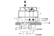
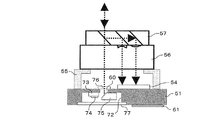
図1は本発明の第1の実施の形態に係る光学モジュールの構成を示す概略図である。また、図2は図1のA−A断面図である。図1及び図2においては、ベース板1の下面側にホルダー部材2を用いて発光装置3が取り付けられている。ベース板1は、平面視長方形の板状に形成されている。ベース板1の上面にはICチップ4が実装されている。また、ベース板1の上面には、ハウジング5を介して、ホログラムレンズ6とプリズム(ビームスプリッタ)7からなる光学ブロックが搭載されている。ICチップ4は、例えばフォトダイオード等の受光素子を内蔵したICチップ(OEIC)であり、本発明における「集積回路素子」に相当する。
図4は本発明の第2の実施の形態に係る光学モジュールの構成を示す概略図である。図4においては、ベース板26の上面にIC(OEIC)チップ27がダイボンディングによって実装され、かつICチップ27にFPC基板28が図示しないバンプを用いて接続されている。ベース板26、ICチップ27及びFPC基板28の各構造に関しては、上記第1の実施の形態と同様であるため、詳細な説明を省略する。また、ベース板26に対するICチップ27の取り付け構造や、ICチップ27に対するFPC基板28の取り付け構造に関しても、上記第1の実施の形態と同様であるため、詳細な説明を省略する。また、本発明の第2の実施の形態においては、ホログラムレンズ及びプリズム(ビームスプリッタ)からなる光学ブロックの図示を省略する。
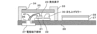
図8は本発明の第2の実施の形態に係る光学モジュールの第1変形例を示す概略図である。この第1変形例においては、前述した第2のサブマウント32を用いることなく、発光素子29を第1のサブマウント31を介してベース板26の上面に実装するとともに、立ち上げミラー30をベース板26の上面に実装している。つまり、発光素子29と立ち上げミラー30を、ベース板26に個別に実装した構成となっている。また、第1のサブマウント31の実装位置と立ち上げミラー30の実装位置との間に貫通穴36を設け、この貫通穴36にセラミックスの積層体からなる電極端子部材37を取り付けて、ワイヤボンディングにより発光素子29と電極端子部材37を電気的に接続している。ワイヤ41の位置は、発光素子29から立ち上げミラー30に向けて出射される光の光路を遮らないように、当該光路に対して、例えば紙面の奥行き方向に位置をずらして設定されている。かかる構成においては、ベース板26上で発光素子29と立ち上げミラー30の光学的な位置合わせを行なうことになる。その場合、周知のレーザカプラの製造プロセスを適用することができる。このため、量産性及び低コスト化の面でメリットがある。
図9は本発明の第2の実施の形態に係る光学モジュールの第2変形例を示す概略図である。この第2変形例においては、上記第1変形例と比較して、電極端子部材37の構成が異なる。すなわち、上記第1変形例においては、セラミックスの積層体によって電極端子部材37を構成しているが、第2変形例においては、シリコンの単層体によって電極端子部材37を構成している。なお、以降の変形例では、セラミックスの積層体によって電極端子部材37を構成した場合について例示するが、いずれの変形例においても、シリコンの単層体によって電極端子部材37を構成することが可能である。
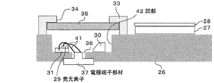
図10は本発明の第2の実施の形態に係る光学モジュールの第3変形例を示す概略図である。この第3変形例においては、ベース板26に凹部42を形成し、この凹部42内に、前述した発光素子29、立ち上げミラー30、第1のサブマウント31及び第2のサブマウント32を実装している。また、ベース板26には、凹部42の底面に開口する状態で貫通穴36を設け、この貫通穴36に電極端子部材37を取り付けて、ワイヤボンディングにより発光素子29と電極端子部材37を電気的に接続している。
図11は本発明の第2の実施の形態に係る光学モジュールの第4変形例を示す概略図である。この第4変形例においては、上記第3変形例と比較して、キャップ部材33を用いることなく、ガラス製の蓋体35を接合層43によりベース板26の上面に直に接合している。接合層43は、高い封止性が得られる低融点ガラスや他の接着剤を用いて形成されている。
図12は本発明の第2の実施の形態に係る光学モジュールの第5変形例を示す概略図である。この第5変形例においては、上記第1変形例と同様に、前述した第2のサブマウント32を用いることなく、発光素子29を第1のサブマウント31を介してベース板26の上面に実装するとともに、立ち上げミラー30をベース板26の上面に実装している。また、第1のサブマウント31の実装位置と立ち上げミラー30の実装位置との間に貫通穴36を設け、この貫通穴36にセラミックスの積層体からなる電極端子部材37を取り付けて、ワイヤボンディングにより発光素子29と電極端子部材37を電気的に接続している。また、第5変形例においては、上記第3変形例と同様に、ベース板26に凹部42を形成し、この凹部42内に、前述した発光素子29、立ち上げミラー30、第1のサブマウント31及び第2のサブマウント32を実装している。また、ベース板26には、凹部42の底面に開口する状態で貫通穴36を設け、この貫通穴36に電極端子部材37を取り付けて、ワイヤボンディングにより発光素子29と電極端子部材37を電気的に接続している。
図13は本発明の第2の実施の形態に係る光学モジュールの第6変形例を示す概略図である。この第6変形例においては、上記第1変形例と同様に、前述した第2のサブマウント32を用いることなく、発光素子29を第1のサブマウント31を介してベース板26の上面に実装するとともに、立ち上げミラー30をベース板26の上面に実装している。また、第1のサブマウント31の実装位置と立ち上げミラー30の実装位置との間に貫通穴36を設け、この貫通穴36にセラミックスの積層体からなる電極端子部材37を取り付けて、ワイヤボンディングにより発光素子29と電極端子部材37を電気的に接続している。また、第5変形例においては、上記第3変形例と同様に、ベース板26に凹部42を形成し、この凹部42内に、前述した発光素子29、立ち上げミラー30、第1のサブマウント31及び第2のサブマウント32を実装している。また、ベース板26には、凹部42の底面に開口する状態で貫通穴36を設け、この貫通穴36に電極端子部材37を取り付けて、ワイヤボンディングにより発光素子29と電極端子部材37を電気的に接続している。さらに、第6変形例においては、上記第4変形例と同様に、キャップ部材33を用いることなく、ガラス製の蓋体35を接合層43によりベース板26の上面に直に接合している。
Claims (7)
- ベース板と、
前記ベース板に実装された発光素子と、
前記ベース板にダイボンディングによって実装され、前記発光素子から出射された光の戻り光を受光部で受光する受光素子内蔵型の集積回路素子と、
光透過用の窓を有し、当該窓を通して前記受光部が露出する状態で前記集積回路素子に接続された回路基板と
を備える光学モジュール。 - 前記ベース板は貫通穴を有し、
前記ベース板の貫通穴の部分に当該貫通穴を塞ぐ状態で取り付けられた電極端子部材を備え、
前記電極端子部材に前記発光素子を電気的に接続してなる
請求項1記載の光学モジュール。 - 前記ベース板を、ダイカスト成形板又はプレス成形板を用いて構成してなる
請求項1又は2記載の光学モジュール。 - 前記集積回路素子と前記回路基板を、超音波実装又は異方導電性実装によって電気的かつ機械的に接続してなる
請求項1又は2記載の光学モジュール。 - 前記発光素子から出射された光を垂直に反射する立ち上げミラーを備え、
前記発光素子と前記立ち上げミラーは、共通のサブマウント材を介して前記ベース板に実装されている
請求項2記載の光学モジュール。 - 前記発光素子から出射された光を垂直に反射する立ち上げミラーを備え、
前記発光素子と前記立ち上げミラーは、前記ベース板に個別に実装されている
請求項2記載の光学モジュール。 - ベース板と、
前記ベース板に実装された発光素子と、
前記ベース板にダイボンディングによって実装され、前記発光素子から出射された光の戻り光を受光部で受光する受光素子内蔵型の集積回路素子と、
光透過用の窓を有し、当該窓を通して前記受光部が露出する状態で前記集積回路素子に接続された回路基板と
を備える光学モジュールを用いた光ピックアップ装置。
Priority Applications (3)
| Application Number | Priority Date | Filing Date | Title |
|---|---|---|---|
| JP2008164136A JP4586896B2 (ja) | 2008-06-24 | 2008-06-24 | 光学モジュール及び光ピックアップ装置 |
| US12/489,740 US7929076B2 (en) | 2008-06-24 | 2009-06-23 | Optical module and optical pickup apparatus |
| CN2009101502625A CN101615399B (zh) | 2008-06-24 | 2009-06-23 | 光学模块和光学拾取装置 |
Applications Claiming Priority (1)
| Application Number | Priority Date | Filing Date | Title |
|---|---|---|---|
| JP2008164136A JP4586896B2 (ja) | 2008-06-24 | 2008-06-24 | 光学モジュール及び光ピックアップ装置 |
Publications (2)
| Publication Number | Publication Date |
|---|---|
| JP2010009633A true JP2010009633A (ja) | 2010-01-14 |
| JP4586896B2 JP4586896B2 (ja) | 2010-11-24 |
Family
ID=41430287
Family Applications (1)
| Application Number | Title | Priority Date | Filing Date |
|---|---|---|---|
| JP2008164136A Expired - Fee Related JP4586896B2 (ja) | 2008-06-24 | 2008-06-24 | 光学モジュール及び光ピックアップ装置 |
Country Status (3)
| Country | Link |
|---|---|
| US (1) | US7929076B2 (ja) |
| JP (1) | JP4586896B2 (ja) |
| CN (1) | CN101615399B (ja) |
Families Citing this family (3)
| Publication number | Priority date | Publication date | Assignee | Title |
|---|---|---|---|---|
| JP5338788B2 (ja) * | 2010-11-10 | 2013-11-13 | 船井電機株式会社 | レーザホルダ、及び、それを備えた光ピックアップ |
| US8469607B2 (en) | 2011-05-09 | 2013-06-25 | Hewlett-Packard Development Company, L.P. | Opto-electronics with compliant electrical contacts |
| CN112397107A (zh) * | 2019-08-16 | 2021-02-23 | 神讯电脑(昆山)有限公司 | 储存装置的加热及散热结构 |
Citations (6)
| Publication number | Priority date | Publication date | Assignee | Title |
|---|---|---|---|---|
| JPH07161065A (ja) * | 1993-10-15 | 1995-06-23 | Sanyo Electric Co Ltd | 光ピックアップ装置 |
| JP2000048391A (ja) * | 1998-07-24 | 2000-02-18 | Fujitsu Ltd | 光集積モジュール |
| JP2000228534A (ja) * | 1999-02-05 | 2000-08-15 | Olympus Optical Co Ltd | 光半導体実装装置 |
| JP2001351266A (ja) * | 2000-04-06 | 2001-12-21 | Fujitsu Ltd | 光ピックアップ及び光記憶装置 |
| JP2006048804A (ja) * | 2004-08-03 | 2006-02-16 | Matsushita Electric Ind Co Ltd | 受光回路実装体 |
| JP2006338848A (ja) * | 2005-06-06 | 2006-12-14 | Sharp Corp | 光集積モジュールおよび光ピックアップ装置 |
Family Cites Families (6)
| Publication number | Priority date | Publication date | Assignee | Title |
|---|---|---|---|---|
| JPH0521655A (ja) * | 1990-11-28 | 1993-01-29 | Mitsubishi Electric Corp | 半導体装置および半導体装置用パツケージ |
| JPH11251373A (ja) | 1998-02-26 | 1999-09-17 | Nippon Denki Factory Engineering Kk | テープキャリアパッケージ |
| DE19961440A1 (de) * | 1999-12-20 | 2001-06-21 | Thomson Brandt Gmbh | Gerät zum Lesen und/oder Schreiben optischer Aufzeichnungsträger |
| JP3517223B2 (ja) * | 2001-04-24 | 2004-04-12 | 株式会社東芝 | 光ディスク装置及び光ディスク処理方法 |
| JP3741108B2 (ja) * | 2003-03-18 | 2006-02-01 | ソニー株式会社 | レーザー発光モジュール |
| JP2007035884A (ja) | 2005-07-26 | 2007-02-08 | Matsushita Electric Ind Co Ltd | 半導体レーザ装置及び半導体レーザ装置の製造方法 |
-
2008
- 2008-06-24 JP JP2008164136A patent/JP4586896B2/ja not_active Expired - Fee Related
-
2009
- 2009-06-23 US US12/489,740 patent/US7929076B2/en not_active Expired - Fee Related
- 2009-06-23 CN CN2009101502625A patent/CN101615399B/zh not_active Expired - Fee Related
Patent Citations (6)
| Publication number | Priority date | Publication date | Assignee | Title |
|---|---|---|---|---|
| JPH07161065A (ja) * | 1993-10-15 | 1995-06-23 | Sanyo Electric Co Ltd | 光ピックアップ装置 |
| JP2000048391A (ja) * | 1998-07-24 | 2000-02-18 | Fujitsu Ltd | 光集積モジュール |
| JP2000228534A (ja) * | 1999-02-05 | 2000-08-15 | Olympus Optical Co Ltd | 光半導体実装装置 |
| JP2001351266A (ja) * | 2000-04-06 | 2001-12-21 | Fujitsu Ltd | 光ピックアップ及び光記憶装置 |
| JP2006048804A (ja) * | 2004-08-03 | 2006-02-16 | Matsushita Electric Ind Co Ltd | 受光回路実装体 |
| JP2006338848A (ja) * | 2005-06-06 | 2006-12-14 | Sharp Corp | 光集積モジュールおよび光ピックアップ装置 |
Also Published As
| Publication number | Publication date |
|---|---|
| CN101615399B (zh) | 2011-07-13 |
| JP4586896B2 (ja) | 2010-11-24 |
| US20090315042A1 (en) | 2009-12-24 |
| US7929076B2 (en) | 2011-04-19 |
| CN101615399A (zh) | 2009-12-30 |
Similar Documents
| Publication | Publication Date | Title |
|---|---|---|
| US6845112B2 (en) | Semiconductor laser and method for manufacturing the same | |
| KR100780522B1 (ko) | 반도체 레이저 | |
| JP3802896B2 (ja) | 半導体レーザ | |
| TWI261245B (en) | Integrated optical device | |
| JP4586896B2 (ja) | 光学モジュール及び光ピックアップ装置 | |
| US20060262820A1 (en) | Semiconductor laser device and optical pickup apparatus having the device | |
| JP4215703B2 (ja) | 光学デバイスおよびその製造方法 | |
| JP2006114096A (ja) | 半導体レーザユニットおよびそれを備えた光ピックアップ装置 | |
| JP7306831B2 (ja) | 半導体パッケージ用ステム、半導体パッケージ | |
| US7280573B2 (en) | Semiconductor laser unit and optical pickup device | |
| CN100395928C (zh) | 半导体激光设备 | |
| JP2007318075A (ja) | 光学デバイス,光学デバイスの製造方法および光ピックアップ装置ならびに光ディスクドライブ装置 | |
| JP2005142294A (ja) | 半導体レーザユニットおよびそれを用いた光ピックアップ装置 | |
| JP2009212524A (ja) | 半導体レーザ | |
| JP2006147751A (ja) | 光半導体装置 | |
| JP2008243869A (ja) | 受光装置 | |
| JP4066375B2 (ja) | 半導体レーザ装置 | |
| JP2008198808A (ja) | 半導体レーザ装置および半導体レーザ装置の製造方法ならびに光ピックアップ装置 | |
| JP2007035884A (ja) | 半導体レーザ装置及び半導体レーザ装置の製造方法 | |
| JP2005293683A (ja) | 光学モジュール及びその製造方法 | |
| JP3477910B2 (ja) | 光ガイド部材及び光ピックアップ | |
| JP2005317646A (ja) | レーザモジュールおよびその製造方法 | |
| JP2006338785A (ja) | 受発光集積装置及び光ディスク装置 | |
| JPH10233029A (ja) | 光ピックアップ装置及びその製造方法 | |
| JPH10256595A (ja) | 半導体装置 |
Legal Events
| Date | Code | Title | Description |
|---|---|---|---|
| RD02 | Notification of acceptance of power of attorney |
Free format text: JAPANESE INTERMEDIATE CODE: A7422 Effective date: 20091021 |
|
| A521 | Written amendment |
Free format text: JAPANESE INTERMEDIATE CODE: A821 Effective date: 20091026 |
|
| RD04 | Notification of resignation of power of attorney |
Free format text: JAPANESE INTERMEDIATE CODE: A7424 Effective date: 20091109 |
|
| A977 | Report on retrieval |
Free format text: JAPANESE INTERMEDIATE CODE: A971007 Effective date: 20100405 |
|
| A131 | Notification of reasons for refusal |
Free format text: JAPANESE INTERMEDIATE CODE: A131 Effective date: 20100413 |
|
| A521 | Written amendment |
Free format text: JAPANESE INTERMEDIATE CODE: A523 Effective date: 20100607 |
|
| TRDD | Decision of grant or rejection written | ||
| A01 | Written decision to grant a patent or to grant a registration (utility model) |
Free format text: JAPANESE INTERMEDIATE CODE: A01 Effective date: 20100810 |
|
| A01 | Written decision to grant a patent or to grant a registration (utility model) |
Free format text: JAPANESE INTERMEDIATE CODE: A01 |
|
| A61 | First payment of annual fees (during grant procedure) |
Free format text: JAPANESE INTERMEDIATE CODE: A61 Effective date: 20100823 |
|
| FPAY | Renewal fee payment (event date is renewal date of database) |
Free format text: PAYMENT UNTIL: 20130917 Year of fee payment: 3 |
|
| R250 | Receipt of annual fees |
Free format text: JAPANESE INTERMEDIATE CODE: R250 |
|
| R250 | Receipt of annual fees |
Free format text: JAPANESE INTERMEDIATE CODE: R250 |
|
| LAPS | Cancellation because of no payment of annual fees |