JP4615707B2 - デュアルダマシン金属化方法 - Google Patents
デュアルダマシン金属化方法 Download PDFInfo
- Publication number
- JP4615707B2 JP4615707B2 JP2000510165A JP2000510165A JP4615707B2 JP 4615707 B2 JP4615707 B2 JP 4615707B2 JP 2000510165 A JP2000510165 A JP 2000510165A JP 2000510165 A JP2000510165 A JP 2000510165A JP 4615707 B2 JP4615707 B2 JP 4615707B2
- Authority
- JP
- Japan
- Prior art keywords
- copper
- layer
- barrier layer
- conductive material
- cvd
- Prior art date
- Legal status (The legal status is an assumption and is not a legal conclusion. Google has not performed a legal analysis and makes no representation as to the accuracy of the status listed.)
- Expired - Fee Related
Links
- 238000000034 method Methods 0.000 title claims description 84
- 230000009977 dual effect Effects 0.000 title claims description 31
- 238000001465 metallisation Methods 0.000 title description 12
- RYGMFSIKBFXOCR-UHFFFAOYSA-N Copper Chemical compound [Cu] RYGMFSIKBFXOCR-UHFFFAOYSA-N 0.000 claims description 107
- 239000010949 copper Substances 0.000 claims description 107
- 229910052802 copper Inorganic materials 0.000 claims description 105
- 238000005229 chemical vapour deposition Methods 0.000 claims description 72
- 229910052751 metal Inorganic materials 0.000 claims description 60
- 239000002184 metal Substances 0.000 claims description 60
- 230000004888 barrier function Effects 0.000 claims description 56
- 238000005240 physical vapour deposition Methods 0.000 claims description 43
- 238000000151 deposition Methods 0.000 claims description 32
- 229910052782 aluminium Inorganic materials 0.000 claims description 17
- XAGFODPZIPBFFR-UHFFFAOYSA-N aluminium Chemical compound [Al] XAGFODPZIPBFFR-UHFFFAOYSA-N 0.000 claims description 17
- 238000009713 electroplating Methods 0.000 claims description 16
- 239000000463 material Substances 0.000 claims description 16
- XUIMIQQOPSSXEZ-UHFFFAOYSA-N Silicon Chemical compound [Si] XUIMIQQOPSSXEZ-UHFFFAOYSA-N 0.000 claims description 10
- NRTOMJZYCJJWKI-UHFFFAOYSA-N Titanium nitride Chemical compound [Ti]#N NRTOMJZYCJJWKI-UHFFFAOYSA-N 0.000 claims description 10
- 229910052710 silicon Inorganic materials 0.000 claims description 10
- 239000010703 silicon Substances 0.000 claims description 10
- MZLGASXMSKOWSE-UHFFFAOYSA-N tantalum nitride Chemical compound [Ta]#N MZLGASXMSKOWSE-UHFFFAOYSA-N 0.000 claims description 10
- -1 tungsten nitride Chemical class 0.000 claims description 10
- 239000000126 substance Substances 0.000 claims description 9
- 229910052715 tantalum Inorganic materials 0.000 claims description 9
- GUVRBAGPIYLISA-UHFFFAOYSA-N tantalum atom Chemical compound [Ta] GUVRBAGPIYLISA-UHFFFAOYSA-N 0.000 claims description 9
- 239000010936 titanium Substances 0.000 claims description 9
- 238000000137 annealing Methods 0.000 claims description 7
- RTAQQCXQSZGOHL-UHFFFAOYSA-N Titanium Chemical compound [Ti] RTAQQCXQSZGOHL-UHFFFAOYSA-N 0.000 claims description 6
- 229910052719 titanium Inorganic materials 0.000 claims description 6
- 229910052721 tungsten Inorganic materials 0.000 claims description 5
- 239000010937 tungsten Substances 0.000 claims description 5
- TWNQGVIAIRXVLR-UHFFFAOYSA-N oxo(oxoalumanyloxy)alumane Chemical compound O=[Al]O[Al]=O TWNQGVIAIRXVLR-UHFFFAOYSA-N 0.000 claims description 3
- HWEYZGSCHQNNEH-UHFFFAOYSA-N silicon tantalum Chemical compound [Si].[Ta] HWEYZGSCHQNNEH-UHFFFAOYSA-N 0.000 claims description 3
- 239000004020 conductor Substances 0.000 claims 14
- 229910052581 Si3N4 Inorganic materials 0.000 claims 2
- HQVNEWCFYHHQES-UHFFFAOYSA-N silicon nitride Chemical compound N12[Si]34N5[Si]62N3[Si]51N64 HQVNEWCFYHHQES-UHFFFAOYSA-N 0.000 claims 2
- 238000009832 plasma treatment Methods 0.000 claims 1
- 230000008569 process Effects 0.000 description 42
- 239000000758 substrate Substances 0.000 description 37
- 239000010408 film Substances 0.000 description 19
- 230000008021 deposition Effects 0.000 description 15
- 239000007789 gas Substances 0.000 description 12
- 230000027756 respiratory electron transport chain Effects 0.000 description 10
- 238000005530 etching Methods 0.000 description 9
- IJGRMHOSHXDMSA-UHFFFAOYSA-N Atomic nitrogen Chemical compound N#N IJGRMHOSHXDMSA-UHFFFAOYSA-N 0.000 description 8
- VYPSYNLAJGMNEJ-UHFFFAOYSA-N Silicium dioxide Chemical compound O=[Si]=O VYPSYNLAJGMNEJ-UHFFFAOYSA-N 0.000 description 8
- 239000002243 precursor Substances 0.000 description 8
- 230000006911 nucleation Effects 0.000 description 7
- 238000010899 nucleation Methods 0.000 description 7
- 238000005498 polishing Methods 0.000 description 7
- 238000001020 plasma etching Methods 0.000 description 6
- 238000001816 cooling Methods 0.000 description 5
- 238000010586 diagram Methods 0.000 description 5
- 238000010438 heat treatment Methods 0.000 description 5
- CSCPPACGZOOCGX-UHFFFAOYSA-N Acetone Chemical compound CC(C)=O CSCPPACGZOOCGX-UHFFFAOYSA-N 0.000 description 4
- KRHYYFGTRYWZRS-UHFFFAOYSA-N Fluorane Chemical compound F KRHYYFGTRYWZRS-UHFFFAOYSA-N 0.000 description 4
- 150000001875 compounds Chemical class 0.000 description 4
- RYGMFSIKBFXOCR-YPZZEJLDSA-N copper-62 Chemical compound [62Cu] RYGMFSIKBFXOCR-YPZZEJLDSA-N 0.000 description 4
- 239000007788 liquid Substances 0.000 description 4
- 229910052757 nitrogen Inorganic materials 0.000 description 4
- 238000000059 patterning Methods 0.000 description 4
- 238000006243 chemical reaction Methods 0.000 description 3
- 239000002131 composite material Substances 0.000 description 3
- 238000000354 decomposition reaction Methods 0.000 description 3
- 239000003989 dielectric material Substances 0.000 description 3
- 238000009792 diffusion process Methods 0.000 description 3
- 239000002019 doping agent Substances 0.000 description 3
- 238000004519 manufacturing process Methods 0.000 description 3
- 230000008018 melting Effects 0.000 description 3
- 238000002844 melting Methods 0.000 description 3
- 150000002739 metals Chemical class 0.000 description 3
- 239000004065 semiconductor Substances 0.000 description 3
- 239000000377 silicon dioxide Substances 0.000 description 3
- 229910052814 silicon oxide Inorganic materials 0.000 description 3
- 238000009736 wetting Methods 0.000 description 3
- XKRFYHLGVUSROY-UHFFFAOYSA-N Argon Chemical compound [Ar] XKRFYHLGVUSROY-UHFFFAOYSA-N 0.000 description 2
- 229910045601 alloy Inorganic materials 0.000 description 2
- 239000000956 alloy Substances 0.000 description 2
- 229910052786 argon Inorganic materials 0.000 description 2
- 230000015572 biosynthetic process Effects 0.000 description 2
- 230000000903 blocking effect Effects 0.000 description 2
- 238000005137 deposition process Methods 0.000 description 2
- 238000007772 electroless plating Methods 0.000 description 2
- 238000005516 engineering process Methods 0.000 description 2
- 230000002708 enhancing effect Effects 0.000 description 2
- 239000010955 niobium Substances 0.000 description 2
- 239000011368 organic material Substances 0.000 description 2
- 239000002245 particle Substances 0.000 description 2
- 238000002310 reflectometry Methods 0.000 description 2
- 235000012239 silicon dioxide Nutrition 0.000 description 2
- 239000007787 solid Substances 0.000 description 2
- WFKWXMTUELFFGS-UHFFFAOYSA-N tungsten Chemical compound [W] WFKWXMTUELFFGS-UHFFFAOYSA-N 0.000 description 2
- 238000007740 vapor deposition Methods 0.000 description 2
- XUBFKJLUXQJJPC-UHFFFAOYSA-N 3,4,5,6,6,7,7-heptafluoro-2-methylnona-2,4-diene Chemical compound CCC(F)(F)C(F)(F)C(F)=C(F)C(F)=C(C)C XUBFKJLUXQJJPC-UHFFFAOYSA-N 0.000 description 1
- QPLDLSVMHZLSFG-UHFFFAOYSA-N Copper oxide Chemical compound [Cu]=O QPLDLSVMHZLSFG-UHFFFAOYSA-N 0.000 description 1
- 239000005751 Copper oxide Substances 0.000 description 1
- 241000283014 Dama Species 0.000 description 1
- UFHFLCQGNIYNRP-UHFFFAOYSA-N Hydrogen Chemical compound [H][H] UFHFLCQGNIYNRP-UHFFFAOYSA-N 0.000 description 1
- 229910008482 TiSiN Inorganic materials 0.000 description 1
- ATJFFYVFTNAWJD-UHFFFAOYSA-N Tin Chemical compound [Sn] ATJFFYVFTNAWJD-UHFFFAOYSA-N 0.000 description 1
- 229910008807 WSiN Inorganic materials 0.000 description 1
- YKTSYUJCYHOUJP-UHFFFAOYSA-N [O--].[Al+3].[Al+3].[O-][Si]([O-])([O-])[O-] Chemical compound [O--].[Al+3].[Al+3].[O-][Si]([O-])([O-])[O-] YKTSYUJCYHOUJP-UHFFFAOYSA-N 0.000 description 1
- 230000001154 acute effect Effects 0.000 description 1
- 150000001336 alkenes Chemical class 0.000 description 1
- 150000001450 anions Chemical class 0.000 description 1
- 230000001174 ascending effect Effects 0.000 description 1
- IVHJCRXBQPGLOV-UHFFFAOYSA-N azanylidynetungsten Chemical compound [W]#N IVHJCRXBQPGLOV-UHFFFAOYSA-N 0.000 description 1
- 230000005540 biological transmission Effects 0.000 description 1
- 239000006227 byproduct Substances 0.000 description 1
- 229910052681 coesite Inorganic materials 0.000 description 1
- 230000001427 coherent effect Effects 0.000 description 1
- 239000000356 contaminant Substances 0.000 description 1
- 229910000431 copper oxide Inorganic materials 0.000 description 1
- 229910052906 cristobalite Inorganic materials 0.000 description 1
- 239000013078 crystal Substances 0.000 description 1
- 230000007547 defect Effects 0.000 description 1
- 238000007872 degassing Methods 0.000 description 1
- JNSGIVNNHKGGRU-JYRVWZFOSA-N diethoxyphosphinothioyl (2z)-2-(2-amino-1,3-thiazol-4-yl)-2-methoxyiminoacetate Chemical compound CCOP(=S)(OCC)OC(=O)C(=N/OC)\C1=CSC(N)=N1 JNSGIVNNHKGGRU-JYRVWZFOSA-N 0.000 description 1
- 238000010494 dissociation reaction Methods 0.000 description 1
- 230000005593 dissociations Effects 0.000 description 1
- 238000001312 dry etching Methods 0.000 description 1
- 230000005684 electric field Effects 0.000 description 1
- GCSJLQSCSDMKTP-UHFFFAOYSA-N ethenyl(trimethyl)silane Chemical compound C[Si](C)(C)C=C GCSJLQSCSDMKTP-UHFFFAOYSA-N 0.000 description 1
- 239000001257 hydrogen Substances 0.000 description 1
- 229910052739 hydrogen Inorganic materials 0.000 description 1
- 238000011065 in-situ storage Methods 0.000 description 1
- 239000011810 insulating material Substances 0.000 description 1
- 230000010354 integration Effects 0.000 description 1
- 230000003993 interaction Effects 0.000 description 1
- QRXWMOHMRWLFEY-UHFFFAOYSA-N isoniazide Chemical compound NNC(=O)C1=CC=NC=C1 QRXWMOHMRWLFEY-UHFFFAOYSA-N 0.000 description 1
- 230000007246 mechanism Effects 0.000 description 1
- QLOAVXSYZAJECW-UHFFFAOYSA-N methane;molecular fluorine Chemical compound C.FF QLOAVXSYZAJECW-UHFFFAOYSA-N 0.000 description 1
- 229910052758 niobium Inorganic materials 0.000 description 1
- GUCVJGMIXFAOAE-UHFFFAOYSA-N niobium atom Chemical compound [Nb] GUCVJGMIXFAOAE-UHFFFAOYSA-N 0.000 description 1
- JRZJOMJEPLMPRA-UHFFFAOYSA-N olefin Natural products CCCCCCCC=C JRZJOMJEPLMPRA-UHFFFAOYSA-N 0.000 description 1
- 229920000620 organic polymer Polymers 0.000 description 1
- 239000011819 refractory material Substances 0.000 description 1
- 230000004044 response Effects 0.000 description 1
- 229910021332 silicide Inorganic materials 0.000 description 1
- FVBUAEGBCNSCDD-UHFFFAOYSA-N silicide(4-) Chemical compound [Si-4] FVBUAEGBCNSCDD-UHFFFAOYSA-N 0.000 description 1
- LIVNPJMFVYWSIS-UHFFFAOYSA-N silicon monoxide Chemical compound [Si-]#[O+] LIVNPJMFVYWSIS-UHFFFAOYSA-N 0.000 description 1
- 238000000992 sputter etching Methods 0.000 description 1
- 229910052682 stishovite Inorganic materials 0.000 description 1
- 239000013077 target material Substances 0.000 description 1
- 239000010409 thin film Substances 0.000 description 1
- NMJKIRUDPFBRHW-UHFFFAOYSA-N titanium Chemical compound [Ti].[Ti] NMJKIRUDPFBRHW-UHFFFAOYSA-N 0.000 description 1
- 229910052905 tridymite Inorganic materials 0.000 description 1
- 239000011800 void material Substances 0.000 description 1
- 238000001039 wet etching Methods 0.000 description 1
Images


Classifications
-
- H—ELECTRICITY
- H01—ELECTRIC ELEMENTS
- H01L—SEMICONDUCTOR DEVICES NOT COVERED BY CLASS H10
- H01L21/00—Processes or apparatus adapted for the manufacture or treatment of semiconductor or solid state devices or of parts thereof
- H01L21/70—Manufacture or treatment of devices consisting of a plurality of solid state components formed in or on a common substrate or of parts thereof; Manufacture of integrated circuit devices or of parts thereof
- H01L21/71—Manufacture of specific parts of devices defined in group H01L21/70
- H01L21/768—Applying interconnections to be used for carrying current between separate components within a device comprising conductors and dielectrics
- H01L21/76801—Applying interconnections to be used for carrying current between separate components within a device comprising conductors and dielectrics characterised by the formation and the after-treatment of the dielectrics, e.g. smoothing
- H01L21/76802—Applying interconnections to be used for carrying current between separate components within a device comprising conductors and dielectrics characterised by the formation and the after-treatment of the dielectrics, e.g. smoothing by forming openings in dielectrics
- H01L21/76807—Applying interconnections to be used for carrying current between separate components within a device comprising conductors and dielectrics characterised by the formation and the after-treatment of the dielectrics, e.g. smoothing by forming openings in dielectrics for dual damascene structures
-
- H—ELECTRICITY
- H01—ELECTRIC ELEMENTS
- H01L—SEMICONDUCTOR DEVICES NOT COVERED BY CLASS H10
- H01L21/00—Processes or apparatus adapted for the manufacture or treatment of semiconductor or solid state devices or of parts thereof
- H01L21/70—Manufacture or treatment of devices consisting of a plurality of solid state components formed in or on a common substrate or of parts thereof; Manufacture of integrated circuit devices or of parts thereof
- H01L21/71—Manufacture of specific parts of devices defined in group H01L21/70
- H01L21/768—Applying interconnections to be used for carrying current between separate components within a device comprising conductors and dielectrics
- H01L21/76838—Applying interconnections to be used for carrying current between separate components within a device comprising conductors and dielectrics characterised by the formation and the after-treatment of the conductors
- H01L21/76841—Barrier, adhesion or liner layers
- H01L21/76843—Barrier, adhesion or liner layers formed in openings in a dielectric
-
- H—ELECTRICITY
- H01—ELECTRIC ELEMENTS
- H01L—SEMICONDUCTOR DEVICES NOT COVERED BY CLASS H10
- H01L21/00—Processes or apparatus adapted for the manufacture or treatment of semiconductor or solid state devices or of parts thereof
- H01L21/70—Manufacture or treatment of devices consisting of a plurality of solid state components formed in or on a common substrate or of parts thereof; Manufacture of integrated circuit devices or of parts thereof
- H01L21/71—Manufacture of specific parts of devices defined in group H01L21/70
- H01L21/768—Applying interconnections to be used for carrying current between separate components within a device comprising conductors and dielectrics
- H01L21/76801—Applying interconnections to be used for carrying current between separate components within a device comprising conductors and dielectrics characterised by the formation and the after-treatment of the dielectrics, e.g. smoothing
- H01L21/76829—Applying interconnections to be used for carrying current between separate components within a device comprising conductors and dielectrics characterised by the formation and the after-treatment of the dielectrics, e.g. smoothing characterised by the formation of thin functional dielectric layers, e.g. dielectric etch-stop, barrier, capping or liner layers
- H01L21/76831—Applying interconnections to be used for carrying current between separate components within a device comprising conductors and dielectrics characterised by the formation and the after-treatment of the dielectrics, e.g. smoothing characterised by the formation of thin functional dielectric layers, e.g. dielectric etch-stop, barrier, capping or liner layers in via holes or trenches, e.g. non-conductive sidewall liners
-
- H—ELECTRICITY
- H01—ELECTRIC ELEMENTS
- H01L—SEMICONDUCTOR DEVICES NOT COVERED BY CLASS H10
- H01L21/00—Processes or apparatus adapted for the manufacture or treatment of semiconductor or solid state devices or of parts thereof
- H01L21/70—Manufacture or treatment of devices consisting of a plurality of solid state components formed in or on a common substrate or of parts thereof; Manufacture of integrated circuit devices or of parts thereof
- H01L21/71—Manufacture of specific parts of devices defined in group H01L21/70
- H01L21/768—Applying interconnections to be used for carrying current between separate components within a device comprising conductors and dielectrics
- H01L21/76838—Applying interconnections to be used for carrying current between separate components within a device comprising conductors and dielectrics characterised by the formation and the after-treatment of the conductors
- H01L21/76841—Barrier, adhesion or liner layers
- H01L21/76853—Barrier, adhesion or liner layers characterized by particular after-treatment steps
- H01L21/76861—Post-treatment or after-treatment not introducing additional chemical elements into the layer
- H01L21/76862—Bombardment with particles, e.g. treatment in noble gas plasmas; UV irradiation
-
- H—ELECTRICITY
- H01—ELECTRIC ELEMENTS
- H01L—SEMICONDUCTOR DEVICES NOT COVERED BY CLASS H10
- H01L21/00—Processes or apparatus adapted for the manufacture or treatment of semiconductor or solid state devices or of parts thereof
- H01L21/70—Manufacture or treatment of devices consisting of a plurality of solid state components formed in or on a common substrate or of parts thereof; Manufacture of integrated circuit devices or of parts thereof
- H01L21/71—Manufacture of specific parts of devices defined in group H01L21/70
- H01L21/768—Applying interconnections to be used for carrying current between separate components within a device comprising conductors and dielectrics
- H01L21/76838—Applying interconnections to be used for carrying current between separate components within a device comprising conductors and dielectrics characterised by the formation and the after-treatment of the conductors
- H01L21/76841—Barrier, adhesion or liner layers
- H01L21/76871—Layers specifically deposited to enhance or enable the nucleation of further layers, i.e. seed layers
- H01L21/76876—Layers specifically deposited to enhance or enable the nucleation of further layers, i.e. seed layers for deposition from the gas phase, e.g. CVD
-
- H—ELECTRICITY
- H01—ELECTRIC ELEMENTS
- H01L—SEMICONDUCTOR DEVICES NOT COVERED BY CLASS H10
- H01L21/00—Processes or apparatus adapted for the manufacture or treatment of semiconductor or solid state devices or of parts thereof
- H01L21/70—Manufacture or treatment of devices consisting of a plurality of solid state components formed in or on a common substrate or of parts thereof; Manufacture of integrated circuit devices or of parts thereof
- H01L21/71—Manufacture of specific parts of devices defined in group H01L21/70
- H01L21/768—Applying interconnections to be used for carrying current between separate components within a device comprising conductors and dielectrics
- H01L21/76838—Applying interconnections to be used for carrying current between separate components within a device comprising conductors and dielectrics characterised by the formation and the after-treatment of the conductors
- H01L21/76877—Filling of holes, grooves or trenches, e.g. vias, with conductive material
Description
【発明の属する技術分野】
本発明は半導体デバイスを製造するための金属化方法に関する。より詳細には、本発明は誘電体層中のデュアルダマシンバイア/ワイヤ輪郭を金属化して金属製の相互接続部と金属バイアプラグを形成する方法に関する。
【0002】
【従来の技術】
サブ半(ハーフ)ミクロンの多レベル金属化方法は、次世代の超大規模集積回路(VLSI)にとって鍵となる技術の1つである。この技術の核心を成す多レベル相互接続では、コンタクト、バイア又は他の外形物を含む、高アスペクト比のアパーチュア内に形成された相互接続部の外形物を平坦化する必要がある。これらの相互接続部外形物を高い信頼性で形成することは、VLSIの成功と、個々の基板とダイス上での回路密度と品質とを向上させるための継続的な努力と、にとって非常に重要なことである。
【0003】
回路密度が高まるに連れて、バイアとコンタクトと他の外形物と、さらにこれら同士間にある誘電体材料との幅は減少しなければならず、この結果、外形物のアスペクト比が増大することになる。したがって、外形物幅対外形物高さの比が4:1以上である高アスペクト比を有する空隙のない外形物を形成しようとする大変な努力が継続されている。このような方法の1つでは、基板表面上にある露出した核生成表面上にある材料に対してだけ選択的に化学的気相堆積法(CVD)が実行される。選択的CVDでは、化学的気相の成分と導電性基板とが接触するところに膜の層が堆積される。この成分はこのような基板上に核生成して金属表面を生成し、この上にさらに堆積プロセスが続く。
【0004】
選択的CVD金属堆積法は、CVD金属前駆気体を分解するには通常は導電性核生成膜からの電子発生源を必要とするという事実に基づいている。従来の選択的CVD金属堆積プロセスによれば、金属は、金属膜と、下地の導電層から出ているドーピングされたシリコン又は金属シリサイドと、のどちらかが露出しているアパーチュアの底部に成長しなければならないのであって、フィールドやアパーチュアの壁などの誘電体表面上に成長してはならない。下地を成す金属膜又はドーピングされたシリコンは、誘電体フィールドやアパーチュアの壁と違って導電性であり、したがって、金属前駆気体の分解に必要な電子を供給し、その結果、金属が堆積される。選択的な堆積をすることによって、非常に小さいディメンジョン(<0.25μm)と高いアスペクト比(>5:1)を持つバイアやコンタクトの開口を充填することが可能なCVD金属をアパーチュア中で「上昇型」(bottom-up)エピタキシャル成長させることができる。
【0005】
単体アルミニウム(Al)とその合金が半導体処理に置いてラインとプラグを形成するために用いられる伝統的な金属であったが、それはアルミニウムの抵抗率が低く、酸化シリコン(SiO2)に対する固着性が優れ、パターン化がし易く、純度が高いからである。さらに、上記の選択的なCVDプロセスを容易化するアルミニウムの前駆気体が入手可能である。しかしながら、アルミニウムは抵抗率が高く電子移動に関して問題がある。電子移動は、金属回路の、その製作の途中で発生する故障に対して、動作中に発生する現象である。電子移動は、回路中で確立された電場で金属が拡散することによって引き起こされる。金属は何時間も動作するうちに一方の端から他方の端に移送し、ついには完全に剥離して回路に開口を空ける。この問題は場合によっては銅のドーピングとテクスチャを改善することによって解決する。しかしながら、電子移動は電流密度が増加するに連れて悪化する問題である。
【0006】
一方、銅とその合金はアルミニウムより抵抗率がさらに低く、電子移動抵抗性はかなり高い。これらの特徴は集積密度が高くなりデバイス速度が速くなるに連れて増す電流密度を支えるためには重要な特徴である。しかしながら、銅金属を多レベル金属化システムに組み込むことにまつわる主要な問題として、(1)エッチング技法を用いて金属をパターン化するのが困難であることと、(2)成熟したCVDプロセスがないのでPVDを用いて小さいバイアを充填するのが困難であること、が挙げられる。サブミクロンという最小外形物寸法であるデバイスにとっては、銅のパターン化のために湿式エッチングを用いることは、液体の表面張力のためと、等方性エッチングプロフィールのためと、過剰エッチングの制御が困難であるためと、信頼性の高い乾式エッチングプロセスがないためと、によって受け入れることができなかった。
【0007】
選択的無電解メッキ法や選択的化学的気相堆積法や高温反応性イオンエッチング法やリフトオフ処理を含む、パターン化された銅製の相互接続部を発生するための方法がいくつか提案されている。無電解メッキ法では、相互接続部の床を床導電性にするように促す必要がある。これで、導電性床を帯電させて、溶液又は浴槽から銅を引き付ける。
【0008】
選択的化学的気相堆積法では一般的には、電導性表面上で金属前駆気体を分解させる。しかしながら、選択的気相堆積法のための、信頼性の高い成熟したプロセスはない。
【0009】
高温反応性イオンエッチング法(RIE)すなわちスパッタエッチング法もまた銅層をパターン化するために用いられてきた。さらに、RIEは、余分の金属を解放層によって構造体からリフトオフして銅の外形物を内部に形成した表面を残すリフトオフ処理法と一緒に用いることができる。
【0010】
銅製の金属配線のためのさらに別の方法は、SiO2などの絶縁性材料製の厚い層内になる溝及び/又はコンタクトをパターン化してエッチングする。この後で、Ti、TiW又はTiNなどのバリヤ金属製の薄い層を絶縁層の頂部並びに溝及び/又はコンタクト内部に設けて拡散バリヤとし、これによって、次いでシリコン中とこのような金属と酸化物間に堆積される予定の金属を内部拡散させてもよい。バリヤ金属が堆積された後で、銅製の層を堆積させて溝を完全に充填する。
【0011】
ある周知の金属化技法は、バイアが下地の層を露出させる床を有する、デュアルダマシンバイア/ワイヤの輪郭を有する誘電体層中にデュアルダマシン相互接続部を形成する方法である。この方法は、バリヤ層に物理的気相堆積法(PVD)を実施するステップと、好ましくは銅である導電性金属に物理的気相堆積法を実施するステップと、次いで、この導電性金属を電気メッキしてバイアと溝を充填するステップと、を含んでいる。最後に、この堆積層と誘電体層とは、化学機械的研磨法などによって平坦化されて導電性ワイヤを輪郭決め(画成)する。
【0012】
図1(a)〜(e)を参照すると、導電性外形物15を含んでいる下地層14の上方に形成された誘電体層16を含む、層化された構造体10の断面図が示されている。下地層14はドーピングされたシリコン基板という形態をとったり又は基板上に最初に形成された又は次いで形成された導電性層であったりする。誘電体層16は技術上周知の手順に従って下地層14の上方に形成し、これによって集積回路全体の1部を形成する。誘電体層16は、ひとたび形成されるとエッチングされてデュアルダマシンバイア/ワイヤ輪郭を形成するが、この場合、バイアは、導電性外形物15の小さい部分を露出する床30を有している。誘電体層16のエッチングは、プラズマエッチングを含むなんらかの誘電体エッチングプロセスによって遂行される。二酸化シリコンと有機材料をエッチングする具体的な技法には、それぞれ緩衝されたフッ化水素酸及びアセトンすなわちEKCなどの化合物を用いる。しかしながら、パターン化は技術上周知の方法を用いて実行され得る。
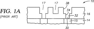
【0013】
図1(a)を参照すると、誘電体層16中に形成されたデュアルダマシンのバイアとワイヤの輪郭の断面図が図示されている。このバイアとワイヤの輪郭によって、下地導電性外形物15との電気的接続部となる導電性相互接続部の堆積が容易となる。この輪郭は、バイア壁34と、導電性外形物15の少なくとも1部分を露出させている床30と、を有するバイア32と;溝壁38を有する溝17と;を提供する。
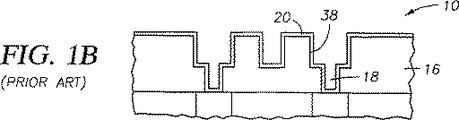
【0014】
図1(b)を参照すると、PVDによるTaN製のバリヤ層20がバイアとワイヤの輪郭上に堆積されてバイア32に穴18を残している。このバリヤ層はチタン、チッ化チタン、タンタル又はチッ化タンタルから形成するのが好ましい。ここで用いられるプロセスはPVDやCVDや合成CVD/PVDであり、これによってテクスチャと膜の特性を向上させる。このバリヤ層が銅の拡散を制限して、相互接続部の信頼性を劇的に向上させる。このバリヤ層は厚さ約25オングストローム(Å)から約400Åであるのが好ましく、約100Åであるのが最も好ましい。
【0015】
図1(c)を参照すると、PVDによる銅製の層21がワイヤ輪郭の壁34及び38及び床30の上方でバリヤ層20上に堆積されている。ここで用いられる金属もまたアルミニウム又はタングステンである。PVD銅層21は追加の金属層に対して良好な固着性を持つ。
【0016】
図1(d)を参照すると、銅22はPVD銅層21の上方で電気メッキされてバイア32を銅プラグ19で充填する。電気メッキは技術上良く知られており、様々な技法によって実行可能である。
【0017】
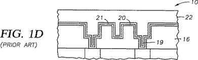
図1(e)を参照すると、次に、構造体10の頂部部分が、好ましくは化学機械的研磨法(CMP)によって平坦化される。この平坦化プロセスの際に、銅層21、22、バリヤ層20及び誘電体16のそれぞれ1部分が構造体の頂部から除去されて、溝を形成された導電性ワイヤ39を持った完全に平坦化された表面を残す。
【0018】
PVD銅堆積と比較して、ブランケットCVDプロセスによって堆積された薄膜は通常はコンフォーマルであり、段差を優れて覆うようになる、すなわち、基板上に形成されたあらゆるアパーチュア、それが非常に小さな形状のアパーチュアであっても、その側部及び基底部上の層の厚さが均一になる。したがって、通常は、ブランケットCVDがアパーチュアを充填するために用いられる方法である。しかしながら、ブランケットCVDプロセスに関連して2つの主要な困難な点がある。第1に、ブランケットCVDによる膜はアパーチュア中のすべての側部から成長し、この結果、堆積層はアパーチュアの上部の角から上向きにそして外向きに成長し、これによって、アパーチュアが完全に充填される前にアパーチュアの上部表面を橋渡しする(すなわち、橋渡し又はクラウニングする)ので、充填されたアパーチュアに空隙を残す。また、連続核生成層、すなわち、CVD層を上に確実に堆積するためのアパーチュア壁上に堆積された基板の全表面の上方で核生成がなされることを保証するための連続膜層によってアパーチュアの幅がさらに減少し、このため、空隙無しでアパーチュアを充填する困難さが増す。第2に、ブランケットCVDによって堆積された膜は、膜が堆積される表面の微細構造に、それが非方向性であったりランダム方向性であったりすると、適合しやすく、この結果、膜の結晶構造の方位がランダムになり、また、低反射性特性となり、電子移動性能が悪化する。
【0019】
選択的CVDは、堆積膜を提供するCVD前駆気体の分解には通常は、導電性核生成膜からの電子の発生源を必要とするという事実に基づいている。従来の選択的CVDプロセスによれば、堆積は、下地層からの導電性膜又はドーピングされたシリコンが露出しているアパーチュアの底部で発生すべきであって、核生成部位が全くない絶縁性のフィールドや絶縁性のアパーチュア壁で発生してはならない。アパーチュアの基底部で露出しているこれらの導電性膜及び/又はドーピングされたシリコンは、誘電体表面とは異なって、前駆気体の分解とこの結果としての膜層の堆積に必要とされる電子を供給する。選択的堆積によって得られる結果は、非常に小さいディメンジョン(<0.25μm)と高いアスペクト比(>5:1)のバイア又はコンタクトを充填することができる、アパーチュア中の膜の「上昇型」成長である。しかしながら、選択的CVDプロセスでは、その表面中の欠陥が存在するフィールド上に好ましくない結節が形成される。
【0020】
一方、PVDプロセスによって、反射性の向上した高方向性膜を堆積できるが、高アスペクト比の場合に適用する場合にはアパーチュアの充填性、すなわち段差の被覆性は良好ではない。目標とする材料を物理的にスパッタリングすると、粒子が基板表面に対して鋭角で走行することになる。その結果、高アスペクト比のアパーチュアを充填している場合、スパッタリングされた粒子は上部壁表面に堆積されて、アパーチュアが堆積材料によって完全に充填される以前にアパーチュアの開口を覆ってしまう傾向がある。この結果得られる構造は一般的に内部に空隙を含んでおり、このため基板上に形成されるデバイスの一貫性を損なう。
【0021】
高アスペクト比のアパーチュアは、膜を高温で堆積させることによってPVDプロセスを用いて充填することができる。1例として、アルミニウムを400℃以上で堆積させて、表面上でとアパーチュア全体にわたるアルミニウムの流れを良くすることができる。この高温アルミニウムプロセスによって段差被覆性が向上することが分かっている。しかしながら、高温アルミニウムプロセスでは、バイアの充填性の信頼性が低く、堆積温度が高く、充填時間が長く、膜の反射性が悪いことがわかった。
【0022】
【発明が解決しようとする課題】
これらの技法は利用可能であるが、なんらかの堆積材料からなる床を有するデュアルダマシン相互接続部とバイアを製作するための金属化プロセスを必要とするものである。このような高度に集積された相互接続部は、特にコンタクト他バイア形成用の高アスペクト比でサブ1/4ミクロン幅のアパーチュアでは空隙のないバイアを提供しなければならない。さらに、より高い電導性と向上した電子移動抵抗性を回路に与えるプロセスが必要である。バイア中に金属プラグを形成し溝中にワイヤを形成するための処理ステップをほとんど必要としない単純なプロセスを有することが好ましい。これがすべて、上記のプロセスによって金属エッチング技法を用いることなく達成されればさらに好ましい。
【0023】
【課題を解決するための手段】
本発明はデュアルバイア/ワイヤ輪郭を有する非導電性層中にデュアルダマシン相互接続部を形成する方法を提供する。本方法は、デュアルダマシンバイア/ワイヤの輪郭内の表面を含む非導電性層の露出表面上にバリヤ層を堆積するステップを含む。次に、このバイア/ワイヤ輪郭を、空隙を防止するアニールステップを間に挟むことが望ましい2つ以上の堆積技法を用いて銅やアルミニウムなどの導電性金属で充填する。最後に、導電性金属とバリヤ層と誘電体層とを、化学機械研磨法などによって平坦化して、下層の導電性領域に対してバイアによって接続される導電性ワイヤを輪郭決めする。
【0024】
【発明の実施の形態】
本発明に関する上記の特徴、利点及び目的が達成される方式が詳細に理解されるように、上記に要約した本発明を添付図面に図示する実施形態を参照して具体的により詳細に説明する。
【0025】
しかしながら、添付図面は本発明の一般的な実施形態を図示するだけであり、したがって、その範囲を限定するものと考えるべきではなく、本発明は他の等しく効果的な実施形態を含むことに注意されたい。
【0026】
本発明は一般的に、相互接続抵抗を減少させ電子移動性能を向上させた交互に集積された構造体中に相互接続部を設ける現場金属化プロセスを提供するものである。より特定的には、本発明は、バイア/ワイヤ輪郭の露出表面上にバリヤ層を組み込んだデュアルダマシン相互接続部と、このバイア/ワイヤ輪郭を充填する2つ以上の堆積技法と、を提供する。非統合技法でも適切な金属相互接続部と金属バイアプラグを提供するとはいえ、好ましい堆積技法を統合処理システムと組み合わせることが可能である。
【0027】
分かりやすいように、本発明は以下に銅堆積技法を参照して説明する。しかしながら、PVDアルミニウム又はアルミニウム/銅などの他の金属プロセスを用いて本発明の利点を遂行してもよい。
【0028】
図2(a)を参照すると、本発明に従ってIC構造体40を形成するには、誘電体層42をパターン化された層の導電性層、すなわち導電性領域46の表面44の上方に従来の技法を用いて形成する。この誘電体層の厚さは単一の金属化層の約2倍であるが、それは、デュアルダマシンバイア/ワイヤ輪郭がその中を通ってエッチングされるからである。現在周知であろうとまだ発見されていなかろうと、フッ素化炭素SiO2や有機ポリマーなどの低誘電体材料を含むいかなる誘電体材料でも用いてよく、それは本発明の範囲内にある。この誘電体層はなんらかの適切な堆積向上性材料の上に体積させてもよいが、好ましい堆積向上性材料には、導電性金属やドーピングされたシリコンなどがある。
【0029】
誘電体層は、ひとたび堆積されると、エッチングされてデュアルダマシンバイア/ワイヤ輪郭を形成するが、この場合、バイア48は低導電性領域46を、充填されるとワイヤ又は相互接続部を形成する溝50に接続している。このバイアは一般的には急峻な側壁52による高アスペクト比を有している。誘電体層42のエッチングは、プラズマエッチングを含むいかなる誘電体エッチングプロセスによって遂行してもよい。二酸化シリコンや有機材料エッチングする具体的な技法には、それぞれ緩衝化されたフッ化水素酸とアセトンすなわちEKCなどの化合物が用いられる。しかしながら、パターン化は技術上周知ないかなる方法を用いて実行してもよい。
【0030】
図2(b)を参照すると、バリヤ層54がバイア48/ワイヤ50輪郭内の表面を含む露出表面上に堆積されている。本発明によれば、好ましいバリヤ/ぬれ性層には、耐火材(例えば、タングステン(W)、窒化タングステン(WN)、ニオブ(Nb)、アルミニウムシリケートなど)、タンタル(Ta)、窒化タンタル(TaN)、窒化チタン(TiN)、もしくはPCV Ti/N2詰めされた3元化合物(例えば、TiSiN、WSiNなど)などの層又はこれらの層の合成物がある。好ましいバリヤ材料には、チタン、窒化チタン、窒化シリコンチタン、窒化タングステン、窒化シリコンタングステン、タンタル、窒化タンタル、窒化シリコンタンタル、ドーピングされたシリコン、アルミニウム、酸化アルミニウムなどがある。最も好ましいバリヤ/ぬれ性材料は、約50Åから約1000Åの厚さを有するPVD層として一般的に提供されるTaやTaNである。逆に、CVD TiN又はWN製のバリヤ/ぬれ性層は一般的に、約100Åから約400Åの厚さを有する。バリヤ/ぬれ性層は堆積されると、誘電体層の上方に実質的に連続したキャップを形成して窒素で処理される。代替法としては、酸化シリコンの露出表面を窒素で処理して、銅に対するバリヤ層として有効なSixOyNzを形成する。
【0031】
バリヤ層とぬれ性層の合成層は、プロセス気体の流れを変えて、CVD銅に対する固着性を向上させることによって生成することができる。例えばWF6、N2、H2及びSiH4を反応させてWNをCVD堆積させることによって、誘電体層に対する固着性が優れたものとなる。堆積の間に窒素の流れを遮断することによって、CVDによるWN層と続いて得られるCVDによる銅層に固着するCVDによるWの最終的なバリヤ/ぬれ性層が得られる。同様に、窒素流を遮断することによって、TaN層をTa層と組み合わせたりTiN層をTi層と組み合わせたりできる。この合成層はCVDによる銅に対する固着性が向上し、これによって、バイア又は溝中に堆積した材料に対するテクスチャが向上する。代替例としては、WN、TaN又はTiNのバリヤ/ぬれ性層をH 2 、Ar又はHeのプラズマで事前処理してCVDによる銅層を核生成して固着性を向上させることもできる。
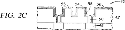
CVD/PVD充填
本発明による一実施形態40では、図2(c)〜(e)にさらに示すように、より低い抵抗率とより大きい電子移動抵抗性を有するデュアルダマシンプラグと相互接続部とを形成する方法が提供される。このサブ半ミクロンのバイアはコンフォーマルCVDによる銅によって空隙無しで充填され、次に溝が、ドーパントとして錫を包含するのが好ましいPVD銅で充填される。堆積後は、このドーパントがCVD銅層中に移動して電子移動抵抗性を向上させる。ワイヤは構造体を平坦化することによって完了される。
【0032】
図2(c)を参照すると、コンフォーマルバリヤ層54を有するデュアルシンバイア/ワイヤ輪郭の断面図が、バイアが銅プラグ60によって完全に充填されるまではフィールド領域56と側壁58との上に均一に堆積されるコンフォーマルCVD銅層55を含んでいるところが図示されている。
【0033】
図2(d)を参照すると、銅層62がCVD銅層の上方に物理的気相堆積されてワイヤ輪郭50を充填している。ワイヤ輪郭を充填するために、一般的に、構造体の全フィールドがPVD銅によって覆われることになる。
【0034】
図2(e)を参照すると、次に、望ましくは化学機械的研磨法(CMP)(例えば、カリフォルニア州サンタクララのアプライドマテリアルズ社(AppliedMaterials)から入手可能なMirra(登録商標)システム)によって構造体の頂部部分が平坦化される。この平坦化プロセス中に、銅62とバリヤ材料54と誘電体42との各部分が構造体の頂部から除去されて、導電性ワイヤ64と66が内部に形成された完全に平坦化された表面が残る。
CVD/アニール/PVD充填
本発明による別の実施形態70では、図3(a)〜(e)に示すように、サブ半ミクロンのバイアがコンフォーマルCVD銅によって部分的に充填されて次にアニールされてバイアを充填している。次に、既述したように溝がPVD銅で充填される。溝の幅が小さい場合、このアニールステップもまた溝を充填する。溝は、溝を下地層に接続するバイアと同じ幅を有してもよい。PVD銅ステップはまた用いてドーパントを提供したり、構造体を平坦化するのに十分な厚さを提供する。
【0035】
図3(a)に、図2(b)に示すものと類似のバリヤ層54を上部に形成したパターン化された誘電体を示す。図3(b)を参照すると、コンフォーマルバリヤ層54を有するデュアルダマシンバイア/ワイヤ輪郭の断面図が、バイアが部分的に充填されて穴74が残るまでフィールド領域56と側壁58上に均一に堆積されるコンフォーマルCVD銅層72を含んでいる。図3(c)を参照すると、次に、CVD銅層が約300℃から約450℃の温度にウエハを加熱することによってアニールされて、銅を穴74中にリフローさせて銅プラグ76を形成する。
【0036】
図3(d)を参照すると、銅層62をCVD銅層の上方に物理的気相堆積されてワイヤ輪郭50を充填する。ワイヤ輪郭を充填するには、一般的に、構造体の全フィールドがPVD銅によって覆われることになる。
【0037】
図3(e)を参照すると、次に、構造体70の頂部部分が、好ましくは化学機械的研磨法(CMP)によって平坦化される。この平坦化プロセスの間に、銅62とバリヤ材料54と誘電体42との各部分が構造体の頂部から除去されて、導電性ワイヤ64と66を内部に形成した完全に平面状の表面を残す。
電子メッキ/PVD又はCVD/PVD充填
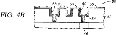
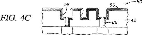
本発明の別の実施形態80では、図4(a)〜(e)に示すように、サブ半ミクロンのバイアが銅の電子メッキ又はコンフォーマルPVD銅によって部分的又は全面的に充填されている。次に、既述したように溝がPVD銅によって非統合システム中で充填される。銅の電子メッキに続いて、PVD銅をドーピングして電子移動性を改善するのが好ましい。ワイヤは構造を平坦化することによって完了される。
【0038】
図4(a)に、図2(b)に示すものと類似のバリヤ層54を上に形成したパターン化された誘電体を示す。図4(b)を参照すると、コンフォーマルバリヤ層54を有するデュアルダマシンバイア/ワイヤ輪郭の断面図が、バイアが部分的に充填されて穴84が残るまで、フィールド領域56と側壁58上に均一に堆積されるコンフォーマル銅電気メッキ層82を含んでいる。図4(c)を参照すると、次に、銅電気メッキ層を約300℃から約450℃の間の温度でウエハを加熱することによってアニールして、銅を穴84中にリフローさせて銅プラグ86を形成する。
【0039】
図4(d)を参照すると、銅層62が銅電気メッキ層の上方に物理的気相堆積されてワイヤ輪郭50を充填している。ワイヤ輪郭を充填するためには、一般的に、構造体の全フィールドがPVD銅によって覆われるということになる。
【0040】
図4(e)を参照すると、次に、構造体80の頂部部分が、好ましくは化学機械的研磨法(CMP)によって平坦化される。この平坦化プロセスの間に、銅62とバリヤ材料54と誘電体42との各部分が構造体の頂部から除去されて、導電性ワイヤ64と66を内部に形成した完全に平面状の表面を残す。
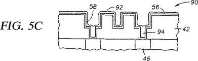
CVD/アニール/電気メッキ
本発明による別の実施形態90では、図5(a)〜(e)に示すように、サブ半ミクロンのバイアがコンフォーマルCVD銅によって部分的に充填され、次に、約300℃から約400℃の間の温度にウエハを加熱することによってアニールされて、銅層の表面を平滑化する。次に、バイアと溝が銅電気メッキで、非統合システム中で充填される。
【0041】
図5(a)に、図2(b)に示すものと類似のバリヤ層54を上に形成したパターン化された誘電体を示す。図5(b)を参照すると、コンフォーマルバリヤ層54を有するデュアルダマシンバイア/ワイヤ輪郭の断面図が、バイアが部分的に充填されて穴94が残るまで、フィールド領域56と側壁58上に均一に堆積されるコンフォーマルCVD銅層92を含んでいる。図5(c)を参照すると、次に、CVD銅層92がアニールされて、穴94を充填することなく銅層を平滑化する。
【0042】
図5(d)を参照すると、銅層62が電気メッキによって堆積されてバイア/ワイヤ輪郭を充填し、これによって銅プラグ96を形成する。ワイヤ輪郭を形成するためには、一般に、構造体の全フィールドが銅で覆われることになる。
【0043】
図5(e)を参照すると、次に、構造体90の頂部部分が、好ましくは化学機械的研磨法(CMP)によって平坦化される。この平坦化の間に、銅62とバリヤ材料54と誘電体42との各部分が構造体の頂部から除去されて、導電性ワイヤ64と66を内部に形成した完全に平面状の表面を残す。
CVD/アニール/CVD/アニール充填
本発明の別の実施形態100では、図6(a)〜(e)に示すように、サブ半ミクロンのバイアがコンフォーマルCVD銅によって部分的に充填され次にアニールされてバイアを充填する。次に、溝がCVD銅によって充填され、次にバイアに対して上記のようにアニールがなされる。ワイヤは構造体を平坦化することによって形成される。
【0044】
図6(a)に、図2(b)に示すものと類似のバリヤ層54を上に形成したパターン化された誘電体を示す。図6(b)を参照すると、コンフォーマルバリヤ層54を有するデュアルダマシンバイア/ワイヤ輪郭の断面図が、バイアが部分的に充填されて穴104が残るまで、フィールド領域56と側壁58上に均一に堆積されるコンフォーマルCVD銅層102を含む。図6(c)を参照すると、次に、CVD銅層を、約300℃から約450℃までの温度にウエハを加熱することによってアニールして、銅を穴104中にリフローして銅プラグ106を形成する。次に、第2のコンフォーマルCVD銅層108が、溝が部分的に充填されて穴110が残るまで、アニール済みのCVD層上に均一に堆積される。図6(d)を参照すると、次に、第2のCVD銅層108を約300℃から約450℃の温度にウエハを加熱することによってアニールして、銅を溝穴110中にリフローして銅ワイヤ112を形成する。図6(e)を参照すると、銅ワイヤ112が前述したように平坦化によって完了される。
統合処理システム
図7を参照すると、上記の統合プロセスをその内部で実現できるPVDチャンバとCVDチャンバの双方と有する統合処理システム160の略図が示されている。一般的には、基板を処理システム160からカセットロードロック162を介して導入して引き込まれる。ブレード167を有するロボット164が処理システム160内に置かれて、基板をシステム160内を移動させる。1つのロボット164がバッファチャンバ168中の一般的な位置に置かれると、カセットロードロック162、脱気ウエハ方向付けチャンバ170、事前清浄化チャンバ172、PVDTiNチャンバ174、冷却チャンバ176の間で基板を伝達する。第2のロボット178が伝達チャンバ180中に位置して、冷却チャンバ176、干渉性のTiチャンバ182、CVDTinチャンバ184、CVD銅チャンバ186及びPVD IMP銅処理チャンバ188との間で基板をやりとりする。統合システム中の伝達チャンバ180は10-3から10-8Torrという低圧又は高圧に維持するのが好ましい。図6に示すチャンバのこの構成は、単一のクラスタツール中でCVDプロセスとPVDプロセスの双方が可能な統合処理システムを含んでいる。この特殊なチャンバ構成すなわち配置は単に図示目的であり、これ以外のPVDプロセスとCVDプロセスの構成が本発明によって考察されている。
【0045】
一般的に、処理システム160中で処理された基板はカセットロードロック162からバッファチャンバ168に送られ、そこで、ロボット164が最初に基板を脱気チャンバ170中に移動させる。次に、基板は事前清浄化チャンバ172、PVD TiNチャンバ174そして次に冷却チャンバ176に伝達される。冷却チャンバ176から、ロボット178は一般的に、基板を冷却チャンバ176に戻す前に、基板を1つ以上の処理チャンバ中とこれら同士間に移動させる。基板が、基板上に所望の構造体を製作するために1つ以上のチャンバ中で何回もそして何らの順序で処理されたり冷却されたりすることが予測される。基板は処理が終わったら処理システム160からバッファチャンバ168を介して取り除かれてロードロック162に移される。マイクロプロセッサコントローラ190が基板上に層を連続して形成するプロセスを制御する。
【0046】
本発明によれば、処理システム160は基板をロードロック162から脱気チャンバ170に移し、基板はここに導入されると汚染物質を脱気する。次に基板は事前清浄化チャンバ172中に移動し、ここで基板表面を清浄化してそのあらゆる汚染物質を除去する。次に基板はCVD−TiNチャンバ175中で処理されて誘電層上にバリヤ層を堆積する。次に、ロボット178は基板をCVD銅174のところに伝達する。基板は2つ以上の金属層を受容して金属製のプラグと相互接続部とを形成する。アニール処理は加熱されたどのチャンバでも発生し得る。金属層が完全に堆積されたら、基板は平坦化ユニットに送られる。
【0047】
多段式真空ウエハ処理システムが、参照してここに組み込まれる、1993年2月16日に発行されたテップマン(Tepman)らによる「多段式真空ウエハ処理のためのシステムと方法(Staged−Vacuum Wafer Processing System and Method)」という名称の米国特許第5,186,718号に開示されている。このシステムはCVDチャンバを収納できるように改良されている。
【0048】
CVD銅層は、Cu+2(hfac)2及びCu+2(fod)2(fodは、ヘプタフルオロジメチルオクタンジエンの略語)を含むなんらかの周知のCVD銅プロセス又は前駆気体を用いて堆積してもよいが、好ましいプロセスでは、揮発性液体錯Cu+1(hfac)とTMVS(hfacはヘキサフルオロアセチルアセトネートアニオンの略語であり、TMVSはトリメチルビニルシランの略語である)を単体気体としてのアルゴンと一緒に用いる。この錯体は周辺状態下の液体であるので、半導体作成に現在用いられている標準のCVD気泡系前駆体送出システムで用いることができる。TMVSとCu+2(hfac)2は双方共がチャンバから排出される堆積反応の揮発性副産物である。この堆積反応は、(s)が表面との相互作用を意味し(g)が気相を意味する次のメカニズムに従って進行すると信じられている:
2Cu+1hfac,TMVS(g) → 2Cu+1hfac,TMVS(s) ステップ(1)
2Cu+1hfac,TMVS(s) → 2Cu+1hfac(s)+2TMVS(g) ステップ(2)
2Cu+1hfac(s) → Cu(s)+Cu+2(hfac)2(g) ステップ(3)
ステップ1では、錯体は気相から金属表面上に吸収される。ステップ2では、配位されたオレフィン(この特定の場合ではTMVS)が錯体から自由気体として解離して、Cu+1hfacを不安定化合物として残す。ステップ3では、Cu+1hfacが解離して銅金属と揮発性Cu+2(hfac)2を生じる。CVD温度での解離は金属表面すなわち電導性表面によって最も強く触媒されるようである。代替の反応では、有機金属銅錯体を水素で還元して金属銅を生じさせることができる。
【0049】
揮発性液体錯体であるCu+1hfacとTMVSとを用いて、銅を熱ベース又はプラズマベースのプロセスのプロセスによって堆積させることができるが、熱ベースのプロセスが最も好ましいものである。プラズマ強化プロセスの場合の基板温度は約100℃と約400℃の間であるのが好ましいが、一方、熱プロセスの場合の基板温度は約50℃から約300℃の間であるが、約170℃が最も好ましい。これらのプロセスの内のどちらかに続いて、CVD銅ぬれ性層を核生成層の上方に備えてもよい。代替例として、電気メッキされた銅をCVD銅ぬれ性層と組み合わせて又はこの代わりに用いてもよい。
【0050】
CVD銅層が堆積されるとそれに続いて、基板がPVD銅チャンバに送られてPVD銅をCVD銅とPVD銅の融点未満の温度で堆積させる。軟金属が銅である場合、PVD銅を約550℃未満、好ましくは約400℃未満のウエハ温度で堆積させるのが好ましい。銅層は約200℃でPVD堆積プロセスの間に流れ始め、タンタルバリヤ/ぬれ性層は本来の場所に固体金属層として固く残る。タンタルは銅とのぬれ性が良好であるので、CVD銅は約400℃ではタンタルを脱ぬれ性することはなく、したがって、先行する技術によるCVDプロセスで教示されるように、アルミニウムの融点を越えるウエハ温度(660℃を越える温度)は必要ない。したがって、薄いタンタル層を付着させることによって、銅の融点の遙か未満の温度で銅の平坦化を達成することができる。
【0051】
本発明のどの態様の場合でも、堆積された銅層をH2でアニールしてこの層を酸化銅の形成に対する抵抗性を強化する。
【0052】
銅の電気メッキはPVD又はCVDより遙かに安価であるが、統合処理システムでは実行できない。幸運にも、基板を別々の処理装置間で伝達する際に基板を空気に露出させても金属層には顕著な界面は形成されなかった。約0.5重量%から約2重量%の錫を包含する目標としての銅を、10-7Torrという真空度と150ECという基板温度でデュアル電子銃を用いて気相堆積すなわち電気メッキさせることができる。
【0053】
前述の説明は本発明の好ましい実施形態を参照したが、本発明の他のそしてさらなる実施形態が本発明の基本的範囲から逸脱することなく可能である。本発明の範囲は以下の請求の範囲によって決定されるものである。
【図面の簡単な説明】
【図1】 (a)〜(e)は、デュアルダマシンバイア/ワイヤ輪郭と、バリヤ層、PVD金属堆積法及び金属電気メッキ法を用いて金属相互接続部を提供する先行技術によるステップと、を示す図である。
【図2】 (a)〜(e)は、本発明の第1の実施形態による、デュアルダマシンバイア/ワイヤ輪郭と、導電性金属でデュアルダマシンバイア/ワイヤ輪郭を充填するに先立ってバリヤ層を堆積するステップと、を示す図である。
【図3】 (a)〜(e)は、本発明の第2の実施形態による、バリヤ層を有するデュアルダマシンバイア/ワイヤ輪郭と、導電性金属を堆積するステップと、を示す図である。
【図4】 (a)〜(e)は、本発明の第3の実施形態による、バリヤ層を有するデュアルダマシンバイア/ワイヤ輪郭と、導電性金属を堆積するステップと、を示す図である。
【図5】 (a)〜(e)は、本発明の第4の実施形態による、バリヤ層を有するデュアルダマシンバイア/ワイヤ輪郭と、導電性金属を堆積するステップと、を示す図である。
【図6】 (a)〜(e)は、本発明の第5の実施形態による、バリヤ層を有するデュアルダマシンバイア/ワイヤ輪郭と、導電性金属を堆積するステップと、を示す図である。
【図7】 本発明の好ましい実施形態による連続金属化用に構成された統合処理システムを示す図である。
Claims (8)
- デュアルダマシンバイア及びワイヤ輪郭を有する誘電体層中にデュアルダマシン相互接続部を形成する方法において、前記方法が:
a)前記誘電体層の露出表面上にバリヤ層を堆積するステップと;
b)前記バリヤ層上で導電性材料の第1部分を電気メッキして、前記バイア輪郭を充填するステップと;
c)前記導電性材料の前記第1部分上に前記導電性材料の第2部分を物理的気相堆積して、前記ワイヤ輪郭を充填するステップと;
d)前記導電性材料と前記バリヤ層とを平坦化するステップと;
を含み、
物理的気相堆積法によって堆積された前記導電性材料の前記第2部分がドーピングされた導電性材料を含み、
前記導電性材料の前記第2部分を堆積する前に、電気メッキによって堆積された前記導電性材料の前記第1部分がアニールされる方法。 - デュアルダマシンバイア及びワイヤ輪郭を有する誘電体層中にデュアルダマシン相互接続部を形成する方法において、前記方法が:
a)前記誘電体層の露出表面上にバリヤ層を堆積するステップと;
b)前記バリヤ層上に導電性材料の第1部分を電気メッキするステップと;
c)前記導電性材料の前記第1部分をアニールして、前記バイア輪郭を充填するステップと;
d)前記導電性材料の前記第1部分上に前記導電性材料の第2部分を物理的気相堆積して、前記ワイヤ輪郭を充填するステップと;
e)前記導電性材料と前記バリヤ層とを平坦化するステップと;
を含む方法。 - 前記物理的気相堆積された導電性材料が銅又はドーピングされた銅である請求項2に記載の方法。
- 前記バリヤ層がチタン、窒化チタン、窒化シリコンチタン、窒化タングステン、窒化シリコンタングステン、タンタル、窒化タンタル、窒化シリコンタンタル、ドーピングされたシリコン、アルミニウム及び酸化アルミニウムからなる群から選択された材料を含む請求項3に記載の方法。
- デュアルダマシンバイア及びワイヤ輪郭を有する誘電体層中にデュアルダマシン相互接続部を形成する方法において、前記方法が:
a)前記誘電体層の露出表面上にバリヤ層を堆積するステップと;
b)前記バリヤ層上に導電性金属のコンフォーマルな第1部分を化学的気相堆積するステップと;
c)前記導電性金属のコンフォーマルな前記第1部分をアニールして、前記導電性金属のコンフォーマルな前記第1部分の表面を平滑化するステップと;
d)前記導電性金属の前記第1部分上に前記導電性金属の第2部分を電気メッキして前記バイア及びワイヤ輪郭を充填するステップと;
e)前記導電性金属と前記バリヤ層とを平坦化するステップと;
を含む方法。 - 前記導電性金属が銅又はドーピングされた銅である請求項5に記載の方法。
- 前記バリヤ層がチタン、窒化チタン、窒化シリコンチタン、窒化タングステン、窒化シリコンタングステン、タンタル、窒化タンタル、窒化シリコンタンタル、ドーピングされたシリコン、アルミニウム及び酸化アルミニウムからなる群から選択された材料を含む請求項5に記載の方法。
- 前記導電性金属のコンフォーマルな第1部分を化学的気相堆積する前に、前記バリヤ層をプラズマ処理に晒すステップをさらに含む請求項5に記載の方法。
Applications Claiming Priority (3)
| Application Number | Priority Date | Filing Date | Title |
|---|---|---|---|
| US08/914,521 US5989623A (en) | 1997-08-19 | 1997-08-19 | Dual damascene metallization |
| US08/914,521 | 1997-08-19 | ||
| PCT/US1998/017010 WO1999009593A1 (en) | 1997-08-19 | 1998-08-17 | Dual damascene metallization |
Publications (3)
| Publication Number | Publication Date |
|---|---|
| JP2001516146A JP2001516146A (ja) | 2001-09-25 |
| JP2001516146A5 JP2001516146A5 (ja) | 2009-11-19 |
| JP4615707B2 true JP4615707B2 (ja) | 2011-01-19 |
Family
ID=25434472
Family Applications (1)
| Application Number | Title | Priority Date | Filing Date |
|---|---|---|---|
| JP2000510165A Expired - Fee Related JP4615707B2 (ja) | 1997-08-19 | 1998-08-17 | デュアルダマシン金属化方法 |
Country Status (6)
| Country | Link |
|---|---|
| US (2) | US5989623A (ja) |
| EP (1) | EP1021827B1 (ja) |
| JP (1) | JP4615707B2 (ja) |
| KR (1) | KR100506139B1 (ja) |
| DE (1) | DE69837674T2 (ja) |
| WO (1) | WO1999009593A1 (ja) |
Families Citing this family (123)
| Publication number | Priority date | Publication date | Assignee | Title |
|---|---|---|---|---|
| US6475903B1 (en) * | 1993-12-28 | 2002-11-05 | Intel Corporation | Copper reflow process |
| US6100196A (en) * | 1996-04-08 | 2000-08-08 | Chartered Semiconductor Manufacturing Ltd. | Method of making a copper interconnect with top barrier layer |
| US6429120B1 (en) | 2000-01-18 | 2002-08-06 | Micron Technology, Inc. | Methods and apparatus for making integrated-circuit wiring from copper, silver, gold, and other metals |
| US6731007B1 (en) * | 1997-08-29 | 2004-05-04 | Hitachi, Ltd. | Semiconductor integrated circuit device with vertically stacked conductor interconnections |
| US6307267B1 (en) * | 1997-12-26 | 2001-10-23 | Kabushiki Kaisha Toshiba | Semiconductor device and manufacturing method thereof |
| US6140234A (en) * | 1998-01-20 | 2000-10-31 | International Business Machines Corporation | Method to selectively fill recesses with conductive metal |
| US7244677B2 (en) | 1998-02-04 | 2007-07-17 | Semitool. Inc. | Method for filling recessed micro-structures with metallization in the production of a microelectronic device |
| WO1999040615A1 (en) | 1998-02-04 | 1999-08-12 | Semitool, Inc. | Method and apparatus for low-temperature annealing of metallization micro-structures in the production of a microelectronic device |
| US6025264A (en) * | 1998-02-09 | 2000-02-15 | United Microelectronics Corp. | Fabricating method of a barrier layer |
| US7034353B2 (en) | 1998-02-27 | 2006-04-25 | Micron Technology, Inc. | Methods for enhancing capacitors having roughened features to increase charge-storage capacity |
| US6150706A (en) | 1998-02-27 | 2000-11-21 | Micron Technology, Inc. | Capacitor/antifuse structure having a barrier-layer electrode and improved barrier layer |
| US6682970B1 (en) | 1998-02-27 | 2004-01-27 | Micron Technology, Inc. | Capacitor/antifuse structure having a barrier-layer electrode and improved barrier layer |
| JP3149846B2 (ja) | 1998-04-17 | 2001-03-26 | 日本電気株式会社 | 半導体装置及びその製造方法 |
| KR100654413B1 (ko) * | 1998-04-30 | 2006-12-05 | 가부시키가이샤 에바라 세이사꾸쇼 | 기판의 도금방법 |
| US6433428B1 (en) * | 1998-05-29 | 2002-08-13 | Kabushiki Kaisha Toshiba | Semiconductor device with a dual damascene type via contact structure and method for the manufacture of same |
| US6475912B1 (en) | 1998-06-01 | 2002-11-05 | Matsushita Electric Industrial Co., Ltd. | Semiconductor device and method and apparatus for fabricating the same while minimizing operating failures and optimizing yield |
| US6355562B1 (en) | 1998-07-01 | 2002-03-12 | Advanced Technology Materials, Inc. | Adhesion promotion method for CVD copper metallization in IC applications |
| KR100265772B1 (ko) * | 1998-07-22 | 2000-10-02 | 윤종용 | 반도체 장치의 배선구조 및 그 제조방법 |
| JP3244058B2 (ja) * | 1998-07-28 | 2002-01-07 | 日本電気株式会社 | 半導体装置の製造方法 |
| US6284656B1 (en) | 1998-08-04 | 2001-09-04 | Micron Technology, Inc. | Copper metallurgy in integrated circuits |
| US6093623A (en) * | 1998-08-04 | 2000-07-25 | Micron Technology, Inc. | Methods for making silicon-on-insulator structures |
| JP2000068230A (ja) * | 1998-08-25 | 2000-03-03 | Mitsubishi Electric Corp | 半導体装置、その製造装置、および、その製造方法 |
| US6380083B1 (en) * | 1998-08-28 | 2002-04-30 | Agere Systems Guardian Corp. | Process for semiconductor device fabrication having copper interconnects |
| JP3187011B2 (ja) * | 1998-08-31 | 2001-07-11 | 日本電気株式会社 | 半導体装置の製造方法 |
| US6288442B1 (en) * | 1998-09-10 | 2001-09-11 | Micron Technology, Inc. | Integrated circuit with oxidation-resistant polymeric layer |
| US5994778A (en) * | 1998-09-18 | 1999-11-30 | Advanced Micro Devices, Inc. | Surface treatment of low-k SiOF to prevent metal interaction |
| JP3180779B2 (ja) * | 1998-10-05 | 2001-06-25 | 日本電気株式会社 | 半導体装置の製造方法 |
| US6153528A (en) * | 1998-10-14 | 2000-11-28 | United Silicon Incorporated | Method of fabricating a dual damascene structure |
| US6080663A (en) * | 1998-11-13 | 2000-06-27 | United Microelectronics Corp. | Dual damascene |
| US6184137B1 (en) * | 1998-11-25 | 2001-02-06 | Applied Materials, Inc. | Structure and method for improving low temperature copper reflow in semiconductor features |
| US6207568B1 (en) * | 1998-11-27 | 2001-03-27 | Taiwan Semiconductor Manufacturing Company | Ionized metal plasma (IMP) method for forming (111) oriented aluminum containing conductor layer |
| US6596637B1 (en) * | 1998-12-07 | 2003-07-22 | Advanced Micro Devices, Inc. | Chemically preventing Cu dendrite formation and growth by immersion |
| US6162728A (en) * | 1998-12-18 | 2000-12-19 | Texas Instruments Incorporated | Method to optimize copper chemical-mechanical polishing in a copper damascene interconnect process for integrated circuit applications |
| US6288449B1 (en) | 1998-12-22 | 2001-09-11 | Agere Systems Guardian Corp. | Barrier for copper metallization |
| KR100280288B1 (ko) | 1999-02-04 | 2001-01-15 | 윤종용 | 반도체 집적회로의 커패시터 제조방법 |
| SG90054A1 (en) * | 1999-02-11 | 2002-07-23 | Chartered Semiconductor Mfg | A new process of dual damascene structure |
| US20020127845A1 (en) * | 1999-03-01 | 2002-09-12 | Paul A. Farrar | Conductive structures in integrated circuits |
| KR100460746B1 (ko) * | 1999-04-13 | 2004-12-09 | 주식회사 하이닉스반도체 | 반도체 소자의 구리 금속 배선 형성 방법 |
| US6103624A (en) * | 1999-04-15 | 2000-08-15 | Advanced Micro Devices, Inc. | Method of improving Cu damascene interconnect reliability by laser anneal before barrier polish |
| US6303496B1 (en) * | 1999-04-27 | 2001-10-16 | Cypress Semiconductor Corporation | Methods of filling constrained spaces with insulating materials and/or of forming contact holes and/or contacts in an integrated circuit |
| US6251772B1 (en) * | 1999-04-29 | 2001-06-26 | Advanced Micro Devicees, Inc. | Dielectric adhesion enhancement in damascene process for semiconductors |
| KR100333712B1 (ko) * | 1999-06-24 | 2002-04-24 | 박종섭 | 반도체 소자의 상감형 금속배선 형성방법 |
| US6251770B1 (en) * | 1999-06-30 | 2001-06-26 | Lam Research Corp. | Dual-damascene dielectric structures and methods for making the same |
| US20040034134A1 (en) * | 1999-08-26 | 2004-02-19 | Lamb James E. | Crosslinkable fill compositions for uniformly protecting via and contact holes |
| CN1196180C (zh) | 1999-08-26 | 2005-04-06 | 部鲁尔科学公司 | 改进的用于双金属镶嵌方法中的填充物料 |
| US6423200B1 (en) * | 1999-09-30 | 2002-07-23 | Lam Research Corporation | Copper interconnect seed layer treatment methods and apparatuses for treating the same |
| US6326297B1 (en) * | 1999-09-30 | 2001-12-04 | Novellus Systems, Inc. | Method of making a tungsten nitride barrier layer with improved adhesion and stability using a silicon layer |
| KR100795534B1 (ko) * | 1999-10-15 | 2008-01-16 | 에이에스엠 인터내셔널 엔.브이. | 상감법 금속화를 위한 균일한 라이닝층 |
| US6361880B1 (en) * | 1999-12-22 | 2002-03-26 | International Business Machines Corporation | CVD/PVD/CVD/PVD fill process |
| KR100338112B1 (ko) * | 1999-12-22 | 2002-05-24 | 박종섭 | 반도체 소자의 구리 금속 배선 형성 방법 |
| US7262130B1 (en) | 2000-01-18 | 2007-08-28 | Micron Technology, Inc. | Methods for making integrated-circuit wiring from copper, silver, gold, and other metals |
| US6376370B1 (en) | 2000-01-18 | 2002-04-23 | Micron Technology, Inc. | Process for providing seed layers for using aluminum, copper, gold and silver metallurgy process for providing seed layers for using aluminum, copper, gold and silver metallurgy |
| US7211512B1 (en) * | 2000-01-18 | 2007-05-01 | Micron Technology, Inc. | Selective electroless-plated copper metallization |
| US6420262B1 (en) * | 2000-01-18 | 2002-07-16 | Micron Technology, Inc. | Structures and methods to enhance copper metallization |
| US6303486B1 (en) * | 2000-01-28 | 2001-10-16 | Advanced Micro Devices, Inc. | Method of fabricating copper-based semiconductor devices using a sacrificial dielectric layer and an unconstrained copper anneal |
| US6355555B1 (en) * | 2000-01-28 | 2002-03-12 | Advanced Micro Devices, Inc. | Method of fabricating copper-based semiconductor devices using a sacrificial dielectric layer |
| US6573030B1 (en) | 2000-02-17 | 2003-06-03 | Applied Materials, Inc. | Method for depositing an amorphous carbon layer |
| DE10008572B4 (de) * | 2000-02-24 | 2007-08-09 | Infineon Technologies Ag | Verbindungseinrichtung für Leistungshalbleitermodule |
| US6384448B1 (en) * | 2000-02-28 | 2002-05-07 | Micron Technology, Inc. | P-channel dynamic flash memory cells with ultrathin tunnel oxides |
| US6639835B2 (en) | 2000-02-29 | 2003-10-28 | Micron Technology, Inc. | Static NVRAM with ultra thin tunnel oxides |
| US6486063B2 (en) * | 2000-03-02 | 2002-11-26 | Tokyo Electron Limited | Semiconductor device manufacturing method for a copper connection |
| US6344125B1 (en) * | 2000-04-06 | 2002-02-05 | International Business Machines Corporation | Pattern-sensitive electrolytic metal plating |
| US6423629B1 (en) * | 2000-05-31 | 2002-07-23 | Kie Y. Ahn | Multilevel copper interconnects with low-k dielectrics and air gaps |
| US6674167B1 (en) * | 2000-05-31 | 2004-01-06 | Micron Technology, Inc. | Multilevel copper interconnect with double passivation |
| US6258709B1 (en) | 2000-06-07 | 2001-07-10 | Micron Technology, Inc. | Formation of electrical interconnect lines by selective metal etch |
| US6346479B1 (en) | 2000-06-14 | 2002-02-12 | Advanced Micro Devices, Inc. | Method of manufacturing a semiconductor device having copper interconnects |
| US6525425B1 (en) * | 2000-06-14 | 2003-02-25 | Advanced Micro Devices, Inc. | Copper interconnects with improved electromigration resistance and low resistivity |
| US6548395B1 (en) * | 2000-11-16 | 2003-04-15 | Advanced Micro Devices, Inc. | Method of promoting void free copper interconnects |
| US6776893B1 (en) | 2000-11-20 | 2004-08-17 | Enthone Inc. | Electroplating chemistry for the CU filling of submicron features of VLSI/ULSI interconnect |
| US7270724B2 (en) | 2000-12-13 | 2007-09-18 | Uvtech Systems, Inc. | Scanning plasma reactor |
| KR100364260B1 (ko) * | 2001-01-05 | 2002-12-11 | 삼성전자 주식회사 | 반도체 집적 회로의 제조 방법 |
| US6773683B2 (en) | 2001-01-08 | 2004-08-10 | Uvtech Systems, Inc. | Photocatalytic reactor system for treating flue effluents |
| US6383920B1 (en) | 2001-01-10 | 2002-05-07 | International Business Machines Corporation | Process of enclosing via for improved reliability in dual damascene interconnects |
| KR100379551B1 (ko) * | 2001-03-09 | 2003-04-10 | 주식회사 하이닉스반도체 | 듀얼 다마신 공정을 이용한 반도체 소자의 제조방법 |
| US7224063B2 (en) | 2001-06-01 | 2007-05-29 | International Business Machines Corporation | Dual-damascene metallization interconnection |
| US20020192944A1 (en) * | 2001-06-13 | 2002-12-19 | Sonderman Thomas J. | Method and apparatus for controlling a thickness of a copper film |
| US6849545B2 (en) * | 2001-06-20 | 2005-02-01 | Applied Materials, Inc. | System and method to form a composite film stack utilizing sequential deposition techniques |
| US20030008243A1 (en) * | 2001-07-09 | 2003-01-09 | Micron Technology, Inc. | Copper electroless deposition technology for ULSI metalization |
| US6692830B2 (en) * | 2001-07-31 | 2004-02-17 | Flex Products, Inc. | Diffractive pigment flakes and compositions |
| US6607976B2 (en) | 2001-09-25 | 2003-08-19 | Applied Materials, Inc. | Copper interconnect barrier layer structure and formation method |
| US6873027B2 (en) | 2001-10-26 | 2005-03-29 | International Business Machines Corporation | Encapsulated energy-dissipative fuse for integrated circuits and method of making the same |
| KR100453957B1 (ko) * | 2001-12-20 | 2004-10-20 | 동부전자 주식회사 | 듀얼 다마신을 이용한 전원 배선 제조 방법 |
| US6620635B2 (en) * | 2002-02-20 | 2003-09-16 | International Business Machines Corporation | Damascene resistor and method for measuring the width of same |
| US6624515B1 (en) * | 2002-03-11 | 2003-09-23 | Micron Technology, Inc. | Microelectronic die including low RC under-layer interconnects |
| US6541397B1 (en) | 2002-03-29 | 2003-04-01 | Applied Materials, Inc. | Removable amorphous carbon CMP stop |
| US6518185B1 (en) * | 2002-04-22 | 2003-02-11 | Advanced Micro Devices, Inc. | Integration scheme for non-feature-size dependent cu-alloy introduction |
| US6656840B2 (en) | 2002-04-29 | 2003-12-02 | Applied Materials Inc. | Method for forming silicon containing layers on a substrate |
| US6620724B1 (en) * | 2002-05-09 | 2003-09-16 | Infineon Technologies Ag | Low resistivity deep trench fill for DRAM and EDRAM applications |
| US6649513B1 (en) | 2002-05-15 | 2003-11-18 | Taiwan Semiconductor Manufacturing Company | Copper back-end-of-line by electropolish |
| KR100456259B1 (ko) * | 2002-07-15 | 2004-11-09 | 주식회사 하이닉스반도체 | 반도체 소자의 구리 배선 형성방법 |
| US6784049B2 (en) * | 2002-08-28 | 2004-08-31 | Micron Technology, Inc. | Method for forming refractory metal oxide layers with tetramethyldisiloxane |
| US7030042B2 (en) * | 2002-08-28 | 2006-04-18 | Micron Technology, Inc. | Systems and methods for forming tantalum oxide layers and tantalum precursor compounds |
| US6709970B1 (en) * | 2002-09-03 | 2004-03-23 | Samsung Electronics Co., Ltd. | Method for creating a damascene interconnect using a two-step electroplating process |
| US6919639B2 (en) * | 2002-10-15 | 2005-07-19 | The Board Of Regents, The University Of Texas System | Multiple copper vias for integrated circuit metallization and methods of fabricating same |
| US6980395B2 (en) * | 2002-10-31 | 2005-12-27 | International Business Machines Corporation | Enhanced coplanar conductance structure for inductive heads |
| US20040108217A1 (en) * | 2002-12-05 | 2004-06-10 | Dubin Valery M. | Methods for forming copper interconnect structures by co-plating of noble metals and structures formed thereby |
| US7273808B1 (en) | 2003-02-03 | 2007-09-25 | Novellus Systems, Inc. | Reactive barrier/seed preclean process for damascene process |
| KR100576363B1 (ko) * | 2003-05-30 | 2006-05-03 | 삼성전자주식회사 | 인시투 화학기상증착 금속 공정 및 그에 사용되는화학기상증착 장비 |
| JP2005039142A (ja) * | 2003-07-18 | 2005-02-10 | Nec Electronics Corp | 半導体装置の製造方法 |
| US7220665B2 (en) | 2003-08-05 | 2007-05-22 | Micron Technology, Inc. | H2 plasma treatment |
| US7026244B2 (en) * | 2003-08-08 | 2006-04-11 | Taiwan Semiconductor Manufacturing Co., Ltd. | Low resistance and reliable copper interconnects by variable doping |
| US7064068B2 (en) * | 2004-01-23 | 2006-06-20 | Taiwan Semiconductor Manufacturing Company, Ltd. | Method to improve planarity of electroplated copper |
| KR100613283B1 (ko) | 2004-12-27 | 2006-08-21 | 동부일렉트로닉스 주식회사 | 반도체 소자의 배선 형성방법 |
| CN1983550A (zh) * | 2005-12-14 | 2007-06-20 | 中芯国际集成电路制造(上海)有限公司 | 提高可靠性和成品率的消除铜位错的方法 |
| US20070281456A1 (en) * | 2006-05-30 | 2007-12-06 | Hynix Semiconductor Inc. | Method of forming line of semiconductor device |
| KR100750950B1 (ko) * | 2006-07-18 | 2007-08-22 | 삼성전자주식회사 | 반도체 장치의 배선 구조물 및 그 형성 방법, 비휘발성메모리 장치 및 그 제조 방법 |
| WO2008084524A1 (ja) * | 2007-01-09 | 2008-07-17 | Fujitsu Microelectronics Limited | 半導体装置の製造方法、および半導体装置の製造装置 |
| KR20090053991A (ko) * | 2007-11-26 | 2009-05-29 | 주식회사 동부하이텍 | 반도체 소자의 제조방법 |
| US20090168247A1 (en) * | 2007-12-28 | 2009-07-02 | Christian Rene Bonhote | Magnetic head with embedded solder connection and method for manufacture thereof |
| US8252653B2 (en) * | 2008-10-21 | 2012-08-28 | Applied Materials, Inc. | Method of forming a non-volatile memory having a silicon nitride charge trap layer |
| US8198671B2 (en) * | 2009-04-22 | 2012-06-12 | Applied Materials, Inc. | Modification of charge trap silicon nitride with oxygen plasma |
| US8575000B2 (en) * | 2011-07-19 | 2013-11-05 | SanDisk Technologies, Inc. | Copper interconnects separated by air gaps and method of making thereof |
| CN102332425A (zh) * | 2011-09-23 | 2012-01-25 | 复旦大学 | 一种提升铜互连技术中抗电迁移特性的方法 |
| US8796853B2 (en) * | 2012-02-24 | 2014-08-05 | International Business Machines Corporation | Metallic capped interconnect structure with high electromigration resistance and low resistivity |
| US8802558B2 (en) | 2012-11-07 | 2014-08-12 | International Business Machines Corporation | Copper interconnect structures and methods of making same |
| US8999767B2 (en) | 2013-01-31 | 2015-04-07 | International Business Machines Corporation | Electronic fuse having an insulation layer |
| EP2779224A3 (en) * | 2013-03-15 | 2014-12-31 | Applied Materials, Inc. | Methods for producing interconnects in semiconductor devices |
| JP6385856B2 (ja) | 2015-02-26 | 2018-09-05 | 東京エレクトロン株式会社 | Cu配線の形成方法および半導体装置の製造方法 |
| US20160276156A1 (en) * | 2015-03-16 | 2016-09-22 | Taiwan Semiconductor Manufacturing Company Ltd. | Semiconductor device and manufacturing process thereof |
| US9704804B1 (en) | 2015-12-18 | 2017-07-11 | Texas Instruments Incorporated | Oxidation resistant barrier metal process for semiconductor devices |
| US11664271B2 (en) | 2019-05-02 | 2023-05-30 | International Business Machines Corporation | Dual damascene with short liner |
| CN112825307B (zh) * | 2019-11-21 | 2022-04-29 | 中芯国际集成电路制造(上海)有限公司 | 一种互连结构的形成方法及互连结构 |
| CN113363204B (zh) * | 2020-03-05 | 2022-04-12 | 中芯国际集成电路制造(深圳)有限公司 | 一种互连结构的形成方法 |
Family Cites Families (41)
| Publication number | Priority date | Publication date | Assignee | Title |
|---|---|---|---|---|
| US5010032A (en) * | 1985-05-01 | 1991-04-23 | Texas Instruments Incorporated | Process for making CMOS device with both P+ and N+ gates including refractory metal silicide and nitride interconnects |
| JPS639925A (ja) * | 1986-06-30 | 1988-01-16 | Nec Corp | 半導体装置の製造方法 |
| JPS6373660A (ja) * | 1986-09-17 | 1988-04-04 | Fujitsu Ltd | 半導体装置 |
| US4960732A (en) * | 1987-02-19 | 1990-10-02 | Advanced Micro Devices, Inc. | Contact plug and interconnect employing a barrier lining and a backfilled conductor material |
| JPS63229814A (ja) * | 1987-03-19 | 1988-09-26 | Nec Corp | 半導体集積回路の製造方法 |
| US4994410A (en) * | 1988-04-04 | 1991-02-19 | Motorola, Inc. | Method for device metallization by forming a contact plug and interconnect using a silicide/nitride process |
| US4938996A (en) * | 1988-04-12 | 1990-07-03 | Ziv Alan R | Via filling by selective laser chemical vapor deposition |
| US4920072A (en) * | 1988-10-31 | 1990-04-24 | Texas Instruments Incorporated | Method of forming metal interconnects |
| US4920073A (en) * | 1989-05-11 | 1990-04-24 | Texas Instruments, Incorporated | Selective silicidation process using a titanium nitride protective layer |
| JPH038359A (ja) * | 1989-06-06 | 1991-01-16 | Fujitsu Ltd | 半導体装置の製造方法 |
| US5091339A (en) * | 1990-07-23 | 1992-02-25 | Microelectronics And Computer Technology Corporation | Trenching techniques for forming vias and channels in multilayer electrical interconnects |
| US5250465A (en) * | 1991-01-28 | 1993-10-05 | Fujitsu Limited | Method of manufacturing semiconductor devices |
| JP2533414B2 (ja) * | 1991-04-09 | 1996-09-11 | 三菱電機株式会社 | 半導体集積回路装置の配線接続構造およびその製造方法 |
| US5292558A (en) * | 1991-08-08 | 1994-03-08 | University Of Texas At Austin, Texas | Process for metal deposition for microelectronic interconnections |
| JPH05206064A (ja) * | 1991-12-10 | 1993-08-13 | Nec Corp | 半導体装置の製造方法 |
| US5300813A (en) * | 1992-02-26 | 1994-04-05 | International Business Machines Corporation | Refractory metal capped low resistivity metal conductor lines and vias |
| US5262354A (en) * | 1992-02-26 | 1993-11-16 | International Business Machines Corporation | Refractory metal capped low resistivity metal conductor lines and vias |
| US5739579A (en) * | 1992-06-29 | 1998-04-14 | Intel Corporation | Method for forming interconnections for semiconductor fabrication and semiconductor device having such interconnections |
| US5354712A (en) * | 1992-11-12 | 1994-10-11 | Northern Telecom Limited | Method for forming interconnect structures for integrated circuits |
| US5439731A (en) * | 1994-03-11 | 1995-08-08 | Cornell Research Goundation, Inc. | Interconnect structures containing blocked segments to minimize stress migration and electromigration damage |
| KR0144956B1 (ko) * | 1994-06-10 | 1998-08-17 | 김광호 | 반도체 장치의 배선 구조 및 그 형성방법 |
| JPH0810693A (ja) * | 1994-06-30 | 1996-01-16 | Dainippon Screen Mfg Co Ltd | レジスト膜の乾燥方法及び装置 |
| US5521119A (en) * | 1994-07-13 | 1996-05-28 | Taiwan Semiconductor Manufacturing Co. | Post treatment of tungsten etching back |
| JPH08181141A (ja) * | 1994-12-21 | 1996-07-12 | Yamaha Corp | 配線形成法 |
| EP0720227B1 (en) * | 1994-12-29 | 2004-12-01 | STMicroelectronics, Inc. | Electrical connection structure on an integrated circuit device comprising a plug with an enlarged head |
| JP3266492B2 (ja) * | 1995-03-02 | 2002-03-18 | 川崎マイクロエレクトロニクス株式会社 | 半導体装置の製造方法 |
| KR100413890B1 (ko) * | 1995-03-02 | 2004-03-19 | 동경 엘렉트론 주식회사 | 반도체장치의제조방법및제조장치 |
| JP2728025B2 (ja) * | 1995-04-13 | 1998-03-18 | 日本電気株式会社 | 半導体装置の製造方法 |
| US5877087A (en) * | 1995-11-21 | 1999-03-02 | Applied Materials, Inc. | Low temperature integrated metallization process and apparatus |
| US5824599A (en) * | 1996-01-16 | 1998-10-20 | Cornell Research Foundation, Inc. | Protected encapsulation of catalytic layer for electroless copper interconnect |
| US5895266A (en) * | 1996-02-26 | 1999-04-20 | Applied Materials, Inc. | Titanium nitride barrier layers |
| US5814557A (en) * | 1996-05-20 | 1998-09-29 | Motorola, Inc. | Method of forming an interconnect structure |
| US5693563A (en) * | 1996-07-15 | 1997-12-02 | Chartered Semiconductor Manufacturing Pte Ltd. | Etch stop for copper damascene process |
| JP3261317B2 (ja) * | 1996-08-30 | 2002-02-25 | 株式会社アルバック | 銅配線製造方法、及び銅配線 |
| JP3281816B2 (ja) * | 1996-09-02 | 2002-05-13 | 株式会社アルバック | 銅配線製造方法 |
| JP2000510289A (ja) * | 1996-12-16 | 2000-08-08 | インターナシヨナル・ビジネス・マシーンズ・コーポレーシヨン | 集積回路チップ上の電気めっき相互接続構造 |
| US5933753A (en) * | 1996-12-16 | 1999-08-03 | International Business Machines Corporation | Open-bottomed via liner structure and method for fabricating same |
| KR100243272B1 (ko) * | 1996-12-20 | 2000-03-02 | 윤종용 | 반도체 소자의 콘택 플러그 형성방법 |
| US5858873A (en) * | 1997-03-12 | 1999-01-12 | Lucent Technologies Inc. | Integrated circuit having amorphous silicide layer in contacts and vias and method of manufacture thereof |
| US5930669A (en) * | 1997-04-03 | 1999-07-27 | International Business Machines Corporation | Continuous highly conductive metal wiring structures and method for fabricating the same |
| JP3390329B2 (ja) * | 1997-06-27 | 2003-03-24 | 日本電気株式会社 | 半導体装置およびその製造方法 |
-
1997
- 1997-08-19 US US08/914,521 patent/US5989623A/en not_active Expired - Lifetime
-
1998
- 1998-08-17 WO PCT/US1998/017010 patent/WO1999009593A1/en active IP Right Grant
- 1998-08-17 EP EP98939967A patent/EP1021827B1/en not_active Expired - Lifetime
- 1998-08-17 KR KR10-2000-7001672A patent/KR100506139B1/ko not_active IP Right Cessation
- 1998-08-17 DE DE69837674T patent/DE69837674T2/de not_active Expired - Fee Related
- 1998-08-17 JP JP2000510165A patent/JP4615707B2/ja not_active Expired - Fee Related
-
1999
- 1999-08-24 US US09/379,696 patent/US6207222B1/en not_active Expired - Fee Related
Also Published As
| Publication number | Publication date |
|---|---|
| KR100506139B1 (ko) | 2005-08-05 |
| DE69837674T2 (de) | 2008-01-10 |
| US6207222B1 (en) | 2001-03-27 |
| US5989623A (en) | 1999-11-23 |
| KR20010023055A (ko) | 2001-03-26 |
| EP1021827B1 (en) | 2007-04-25 |
| WO1999009593A1 (en) | 1999-02-25 |
| EP1021827A1 (en) | 2000-07-26 |
| DE69837674D1 (de) | 2007-06-06 |
| JP2001516146A (ja) | 2001-09-25 |
Similar Documents
| Publication | Publication Date | Title |
|---|---|---|
| JP4615707B2 (ja) | デュアルダマシン金属化方法 | |
| US7112528B2 (en) | Fully planarized dual damascene metallization using copper line interconnect and selective CVD aluminum plug | |
| US7470612B2 (en) | Method of forming metal wiring layer of semiconductor device | |
| US7550386B2 (en) | Advanced seed layers for interconnects | |
| US6077781A (en) | Single step process for blanket-selective CVD aluminum deposition | |
| US6924226B2 (en) | Methods for making multiple seed layers for metallic interconnects | |
| US6955983B2 (en) | Methods of forming metal interconnections of semiconductor devices by treating a barrier metal layer | |
| US8586471B2 (en) | Seed layers for metallic interconnects and products | |
| JP2001516146A5 (ja) | ||
| US6110828A (en) | In-situ capped aluminum plug (CAP) process using selective CVD AL for integrated plug/interconnect metallization | |
| US6066358A (en) | Blanket-selective chemical vapor deposition using an ultra-thin nucleation layer | |
| US6069072A (en) | CVD tin barrier layer for reduced electromigration of aluminum plugs | |
| US20030073304A1 (en) | Selective tungsten stud as copper diffusion barrier to silicon contact | |
| US6605531B1 (en) | Hole-filling technique using CVD aluminum and PVD aluminum integration | |
| JPH10116800A (ja) | 温間pvdアルミニウムでcvdアルミニウム選択性ロスをなくすためのプロセス |
Legal Events
| Date | Code | Title | Description |
|---|---|---|---|
| A621 | Written request for application examination |
Free format text: JAPANESE INTERMEDIATE CODE: A621 Effective date: 20050801 |
|
| A977 | Report on retrieval |
Free format text: JAPANESE INTERMEDIATE CODE: A971007 Effective date: 20081224 |
|
| A131 | Notification of reasons for refusal |
Free format text: JAPANESE INTERMEDIATE CODE: A131 Effective date: 20090401 |
|
| A601 | Written request for extension of time |
Free format text: JAPANESE INTERMEDIATE CODE: A601 Effective date: 20090701 |
|
| A602 | Written permission of extension of time |
Free format text: JAPANESE INTERMEDIATE CODE: A602 Effective date: 20090708 |
|
| A601 | Written request for extension of time |
Free format text: JAPANESE INTERMEDIATE CODE: A601 Effective date: 20090730 |
|
| A602 | Written permission of extension of time |
Free format text: JAPANESE INTERMEDIATE CODE: A602 Effective date: 20090806 |
|
| A601 | Written request for extension of time |
Free format text: JAPANESE INTERMEDIATE CODE: A601 Effective date: 20090831 |
|
| A602 | Written permission of extension of time |
Free format text: JAPANESE INTERMEDIATE CODE: A602 Effective date: 20090907 |
|
| A524 | Written submission of copy of amendment under article 19 pct |
Free format text: JAPANESE INTERMEDIATE CODE: A524 Effective date: 20090928 |
|
| RD03 | Notification of appointment of power of attorney |
Free format text: JAPANESE INTERMEDIATE CODE: A7423 Effective date: 20090928 |
|
| A02 | Decision of refusal |
Free format text: JAPANESE INTERMEDIATE CODE: A02 Effective date: 20091215 |
|
| A521 | Request for written amendment filed |
Free format text: JAPANESE INTERMEDIATE CODE: A523 Effective date: 20100312 |
|
| A911 | Transfer to examiner for re-examination before appeal (zenchi) |
Free format text: JAPANESE INTERMEDIATE CODE: A911 Effective date: 20100422 |
|
| A131 | Notification of reasons for refusal |
Free format text: JAPANESE INTERMEDIATE CODE: A131 Effective date: 20100601 |
|
| A521 | Request for written amendment filed |
Free format text: JAPANESE INTERMEDIATE CODE: A523 Effective date: 20100804 |
|
| TRDD | Decision of grant or rejection written | ||
| A01 | Written decision to grant a patent or to grant a registration (utility model) |
Free format text: JAPANESE INTERMEDIATE CODE: A01 Effective date: 20100928 |
|
| A01 | Written decision to grant a patent or to grant a registration (utility model) |
Free format text: JAPANESE INTERMEDIATE CODE: A01 |
|
| A61 | First payment of annual fees (during grant procedure) |
Free format text: JAPANESE INTERMEDIATE CODE: A61 Effective date: 20101021 |
|
| R150 | Certificate of patent or registration of utility model |
Free format text: JAPANESE INTERMEDIATE CODE: R150 |
|
| FPAY | Renewal fee payment (event date is renewal date of database) |
Free format text: PAYMENT UNTIL: 20131029 Year of fee payment: 3 |
|
| FPAY | Renewal fee payment (event date is renewal date of database) |
Free format text: PAYMENT UNTIL: 20131029 Year of fee payment: 3 |
|
| RD02 | Notification of acceptance of power of attorney |
Free format text: JAPANESE INTERMEDIATE CODE: R3D02 |
|
| LAPS | Cancellation because of no payment of annual fees |