JP2012129557A - 露光方法及び露光装置、並びにデバイス製造方法 - Google Patents
露光方法及び露光装置、並びにデバイス製造方法 Download PDFInfo
- Publication number
- JP2012129557A JP2012129557A JP2012079177A JP2012079177A JP2012129557A JP 2012129557 A JP2012129557 A JP 2012129557A JP 2012079177 A JP2012079177 A JP 2012079177A JP 2012079177 A JP2012079177 A JP 2012079177A JP 2012129557 A JP2012129557 A JP 2012129557A
- Authority
- JP
- Japan
- Prior art keywords
- liquid
- exposure apparatus
- exposure
- film
- wafer
- Prior art date
- Legal status (The legal status is an assumption and is not a legal conclusion. Google has not performed a legal analysis and makes no representation as to the accuracy of the status listed.)
- Granted
Links
Images


Classifications
-
- G—PHYSICS
- G03—PHOTOGRAPHY; CINEMATOGRAPHY; ANALOGOUS TECHNIQUES USING WAVES OTHER THAN OPTICAL WAVES; ELECTROGRAPHY; HOLOGRAPHY
- G03F—PHOTOMECHANICAL PRODUCTION OF TEXTURED OR PATTERNED SURFACES, e.g. FOR PRINTING, FOR PROCESSING OF SEMICONDUCTOR DEVICES; MATERIALS THEREFOR; ORIGINALS THEREFOR; APPARATUS SPECIALLY ADAPTED THEREFOR
- G03F7/00—Photomechanical, e.g. photolithographic, production of textured or patterned surfaces, e.g. printing surfaces; Materials therefor, e.g. comprising photoresists; Apparatus specially adapted therefor
- G03F7/70—Microphotolithographic exposure; Apparatus therefor
- G03F7/70483—Information management; Active and passive control; Testing; Wafer monitoring, e.g. pattern monitoring
- G03F7/70605—Workpiece metrology
- G03F7/70608—Monitoring the unpatterned workpiece, e.g. measuring thickness, reflectivity or effects of immersion liquid on resist
-
- H—ELECTRICITY
- H01—ELECTRIC ELEMENTS
- H01L—SEMICONDUCTOR DEVICES NOT COVERED BY CLASS H10
- H01L21/00—Processes or apparatus adapted for the manufacture or treatment of semiconductor or solid state devices or of parts thereof
- H01L21/02—Manufacture or treatment of semiconductor devices or of parts thereof
- H01L21/027—Making masks on semiconductor bodies for further photolithographic processing not provided for in group H01L21/18 or H01L21/34
- H01L21/0271—Making masks on semiconductor bodies for further photolithographic processing not provided for in group H01L21/18 or H01L21/34 comprising organic layers
- H01L21/0273—Making masks on semiconductor bodies for further photolithographic processing not provided for in group H01L21/18 or H01L21/34 comprising organic layers characterised by the treatment of photoresist layers
-
- G—PHYSICS
- G03—PHOTOGRAPHY; CINEMATOGRAPHY; ANALOGOUS TECHNIQUES USING WAVES OTHER THAN OPTICAL WAVES; ELECTROGRAPHY; HOLOGRAPHY
- G03F—PHOTOMECHANICAL PRODUCTION OF TEXTURED OR PATTERNED SURFACES, e.g. FOR PRINTING, FOR PROCESSING OF SEMICONDUCTOR DEVICES; MATERIALS THEREFOR; ORIGINALS THEREFOR; APPARATUS SPECIALLY ADAPTED THEREFOR
- G03F7/00—Photomechanical, e.g. photolithographic, production of textured or patterned surfaces, e.g. printing surfaces; Materials therefor, e.g. comprising photoresists; Apparatus specially adapted therefor
- G03F7/20—Exposure; Apparatus therefor
- G03F7/2041—Exposure; Apparatus therefor in the presence of a fluid, e.g. immersion; using fluid cooling means
-
- G—PHYSICS
- G03—PHOTOGRAPHY; CINEMATOGRAPHY; ANALOGOUS TECHNIQUES USING WAVES OTHER THAN OPTICAL WAVES; ELECTROGRAPHY; HOLOGRAPHY
- G03F—PHOTOMECHANICAL PRODUCTION OF TEXTURED OR PATTERNED SURFACES, e.g. FOR PRINTING, FOR PROCESSING OF SEMICONDUCTOR DEVICES; MATERIALS THEREFOR; ORIGINALS THEREFOR; APPARATUS SPECIALLY ADAPTED THEREFOR
- G03F7/00—Photomechanical, e.g. photolithographic, production of textured or patterned surfaces, e.g. printing surfaces; Materials therefor, e.g. comprising photoresists; Apparatus specially adapted therefor
- G03F7/70—Microphotolithographic exposure; Apparatus therefor
- G03F7/70216—Mask projection systems
- G03F7/70341—Details of immersion lithography aspects, e.g. exposure media or control of immersion liquid supply
-
- G—PHYSICS
- G03—PHOTOGRAPHY; CINEMATOGRAPHY; ANALOGOUS TECHNIQUES USING WAVES OTHER THAN OPTICAL WAVES; ELECTROGRAPHY; HOLOGRAPHY
- G03F—PHOTOMECHANICAL PRODUCTION OF TEXTURED OR PATTERNED SURFACES, e.g. FOR PRINTING, FOR PROCESSING OF SEMICONDUCTOR DEVICES; MATERIALS THEREFOR; ORIGINALS THEREFOR; APPARATUS SPECIALLY ADAPTED THEREFOR
- G03F7/00—Photomechanical, e.g. photolithographic, production of textured or patterned surfaces, e.g. printing surfaces; Materials therefor, e.g. comprising photoresists; Apparatus specially adapted therefor
- G03F7/70—Microphotolithographic exposure; Apparatus therefor
- G03F7/708—Construction of apparatus, e.g. environment aspects, hygiene aspects or materials
- G03F7/70858—Environment aspects, e.g. pressure of beam-path gas, temperature
-
- G—PHYSICS
- G03—PHOTOGRAPHY; CINEMATOGRAPHY; ANALOGOUS TECHNIQUES USING WAVES OTHER THAN OPTICAL WAVES; ELECTROGRAPHY; HOLOGRAPHY
- G03F—PHOTOMECHANICAL PRODUCTION OF TEXTURED OR PATTERNED SURFACES, e.g. FOR PRINTING, FOR PROCESSING OF SEMICONDUCTOR DEVICES; MATERIALS THEREFOR; ORIGINALS THEREFOR; APPARATUS SPECIALLY ADAPTED THEREFOR
- G03F7/00—Photomechanical, e.g. photolithographic, production of textured or patterned surfaces, e.g. printing surfaces; Materials therefor, e.g. comprising photoresists; Apparatus specially adapted therefor
- G03F7/70—Microphotolithographic exposure; Apparatus therefor
- G03F7/708—Construction of apparatus, e.g. environment aspects, hygiene aspects or materials
- G03F7/7095—Materials, e.g. materials for housing, stage or other support having particular properties, e.g. weight, strength, conductivity, thermal expansion coefficient
-
- H—ELECTRICITY
- H01—ELECTRIC ELEMENTS
- H01L—SEMICONDUCTOR DEVICES NOT COVERED BY CLASS H10
- H01L21/00—Processes or apparatus adapted for the manufacture or treatment of semiconductor or solid state devices or of parts thereof
- H01L21/02—Manufacture or treatment of semiconductor devices or of parts thereof
- H01L21/027—Making masks on semiconductor bodies for further photolithographic processing not provided for in group H01L21/18 or H01L21/34
- H01L21/0271—Making masks on semiconductor bodies for further photolithographic processing not provided for in group H01L21/18 or H01L21/34 comprising organic layers
- H01L21/0273—Making masks on semiconductor bodies for further photolithographic processing not provided for in group H01L21/18 or H01L21/34 comprising organic layers characterised by the treatment of photoresist layers
- H01L21/0274—Photolithographic processes
Landscapes
- General Physics & Mathematics (AREA)
- Physics & Mathematics (AREA)
- Engineering & Computer Science (AREA)
- Health & Medical Sciences (AREA)
- Environmental & Geological Engineering (AREA)
- Public Health (AREA)
- Epidemiology (AREA)
- Atmospheric Sciences (AREA)
- Toxicology (AREA)
- Life Sciences & Earth Sciences (AREA)
- Condensed Matter Physics & Semiconductors (AREA)
- Manufacturing & Machinery (AREA)
- Computer Hardware Design (AREA)
- Microelectronics & Electronic Packaging (AREA)
- Power Engineering (AREA)
- Exposure And Positioning Against Photoresist Photosensitive Materials (AREA)
- Exposure Of Semiconductors, Excluding Electron Or Ion Beam Exposure (AREA)
- Container, Conveyance, Adherence, Positioning, Of Wafer (AREA)
Abstract
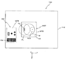
【解決手段】 液浸装置132は、投影光学系PLの光射出側に配置される物体(部材)表面の撥液膜上に供給される液体にその液体の比抵抗を調整する所定の物質を混入して溶解させる混入機構を有し、その所定の物質を溶解させた液体Lqを撥液膜上に供給して液浸領域を形成する。
【選択図】図1
Description
Claims (29)
- 液体を介して物体を露光する露光方法であって、
液体にその液体の比抵抗を調整する所定の物質を溶解させ、その所定の物質を溶解させた液体を前記物体上に形成された膜上に供給して液浸領域を形成する工程と、
前記液体を介して露光光を前記物体上に照射して露光し、所定のパターンを形成する工程と、
を含む露光方法。 - 請求項1に記載の露光方法において、
前記物体上の膜は、前記パターンを形成するための感応材で形成されていることを特徴とする露光方法。 - 請求項2に記載の露光方法において、
前記物体上の膜は、前記液浸領域を形成する液体に対して撥液性であることを特徴とする露光方法。 - 請求項1に記載の露光方法において、
前記物体上の膜は、前記パターンを形成するための感応材を覆うように形成されていることを特徴とする露光方法。 - 請求項4に記載の露光方法において、
前記物体上の膜は、前記液浸領域を形成する液体に対して撥液性であることを特徴とする露光方法。 - 請求項1に記載の露光方法において、
前記液体の比抵抗を調整することによって、前記液体の帯電に起因する前記物体上の膜の劣化を防止することを特徴とする露光方法。 - 請求項1に記載の露光方法において、
前記所定の物質は、二酸化炭素を含むことを特徴とする露光方法。 - 請求項1〜7のいずれか一項に記載の露光方法を用いて物体を露光することによって、前記物体上にデバイスパターンを形成するリソグラフィ工程を含むデバイス製造方法。
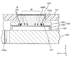
- 光学部材及び液体を介して物体に露光ビームを照射して、前記物体を露光することによって、該物体上に所定のパターンを形成する露光装置であって、
前記光学部材の光射出側に配置される部材表面の撥液膜と、該撥液膜上の液体とを介して、露光ビームと同一波長の光を受光するセンサと、
前記撥液膜上に供給される液体にその液体の比抵抗を調整する所定の物質を混入して溶解させる混入機構を有し、その所定の物質を溶解させた前記液体を前記撥液膜上に供給して液浸領域を形成する液浸装置と、を備える露光装置。 - 請求項9に記載の露光装置において、
前記物体が載置される物体ステージを更に備え、
前記部材が、前記物体ステージ上に設けられていることを特徴とする露光装置。 - 請求項9に記載の露光装置において、
前記物体が載置される物体ステージと、
前記部材が設けられた、前記物体ステージとは異なる計測ステージと、を更に備える露光装置。 - 請求項10に記載の露光装置において、
前記物体ステージ上の物体及び前記物体ステージ上の前記液体に接する部材の少なくとも1つが接地されていることを特徴とする露光装置。 - 請求項10に記載の露光装置において、
前記物体に接する前記物体ステージの一部が導電性材料で形成されていることを特徴とする露光装置。 - 請求項9に記載の露光装置において、
前記液体の比抵抗を調整することによって、前記液体の帯電に起因する前記撥液膜の劣化を防止することを特徴とする露光装置。 - 請求項9に記載の露光装置において、
前記所定の物質の溶解に起因する前記液体の屈折率変動を考慮して光学系の少なくとも一部を調整する調整装置を更に備える露光装置。 - 請求項9に記載の露光装置において、
前記所定の物質の溶解に起因する前記液体の前記露光ビームと同一波長の光に対する透過率変動を考慮して前記物体に対するドーズ制御を行う制御装置を更に備える露光装置。 - 請求項9に記載の露光装置において、
前記所定の物質は、二酸化炭素を含むことを特徴とする露光装置。 - 液体を介して物体に露光ビームを照射して前記物体を露光することによって、該物体上に所定のパターンを形成する露光装置であって、
前記物体が載置される物体ステージと、
前記物体ステージ上に載置された前記物体上に形成された所定の膜上に供給される液体にその液体の比抵抗を調整する所定の物質を混入して溶解させる混入機構を有し、その所定の物質を溶解させた前記液体を前記膜上に供給して液浸領域を形成する液浸装置と、を備える露光装置。 - 請求項18に記載の露光装置において、
前記液浸装置は、前記液体を前記膜上に供給する供給部材と、該供給部材に送られる液体の温度調整及び流量制御の少なくとも一方を行う液体調整機構とを更に有し、
前記混入機構は、前記液体調整機構と前記供給部材との間及び前記液体調整機構の上流側の一方で前記液体中に所定の物質を混入して溶解させることを特徴とする露光装置。 - 請求項19に記載の露光装置において、
前記物体及び前記供給部材の少なくとも1つが接地されていることを特徴とする露光装置。 - 請求項18に記載の露光装置において、
前記物体に接する前記物体ステージの一部が導電性材料で形成されていることを特徴とする露光装置。 - 請求項18に記載の露光装置において、
前記液体の比抵抗を調整することによって、前記液体の帯電に起因する前記物体上の膜の劣化を防止することを特徴とする露光装置。 - 請求項18に記載の露光装置において、
前記所定の物質の溶解に起因する前記液体の屈折率変動を考慮して光学系の少なくとも一部を調整する調整装置を更に備える露光装置。 - 請求項18に記載の露光装置において、
前記所定の物質の溶解に起因する前記液体の前記露光ビームと同一波長の光に対する透過率変動を考慮して前記物体に対するドーズ制御を行う制御装置を更に備える露光装置。 - 請求項18に記載の露光装置において、
前記所定の物質は、二酸化炭素を含むことを特徴とする露光装置。 - 請求項9〜25のいずれか一項に記載の露光装置を用いて物体上にデバイスパターンを形成するリソグラフィ工程を含むデバイス製造方法。
- 基板処理装置に接続された露光装置内で、液体を介して物体を露光し、物体上にデバイスパターンを形成するリソグラフィ工程を含むデバイス製造方法であって、
前記露光装置内に搬入される前の物体を導電性の液体でソークして、前記物体に帯電した電荷を除去することを特徴とするデバイス製造方法。 - 請求項27に記載のデバイス製造方法において、
前記導電性の液体による前記物体のソークは、前記基板処理装置内で行われることを特徴とするデバイス製造方法。 - 請求項27又は28に記載のデバイス製造方法において、
前記基板処理装置内で前記物体にレジスト膜が形成されることを特徴とするデバイス製造方法。
Priority Applications (1)
| Application Number | Priority Date | Filing Date | Title |
|---|---|---|---|
| JP2012079177A JP5594653B2 (ja) | 2005-04-25 | 2012-03-30 | 露光方法及び露光装置 |
Applications Claiming Priority (5)
| Application Number | Priority Date | Filing Date | Title |
|---|---|---|---|
| JP2005127025 | 2005-04-25 | ||
| JP2005127025 | 2005-04-25 | ||
| JP2005238373 | 2005-08-19 | ||
| JP2005238373 | 2005-08-19 | ||
| JP2012079177A JP5594653B2 (ja) | 2005-04-25 | 2012-03-30 | 露光方法及び露光装置 |
Related Parent Applications (1)
| Application Number | Title | Priority Date | Filing Date |
|---|---|---|---|
| JP2010173281A Division JP5594646B2 (ja) | 2005-04-25 | 2010-08-02 | 露光装置及び露光装置の制御方法 |
Related Child Applications (1)
| Application Number | Title | Priority Date | Filing Date |
|---|---|---|---|
| JP2013257558A Division JP5831825B2 (ja) | 2005-04-25 | 2013-12-13 | 露光装置及び液体供給方法 |
Publications (3)
| Publication Number | Publication Date |
|---|---|
| JP2012129557A true JP2012129557A (ja) | 2012-07-05 |
| JP2012129557A5 JP2012129557A5 (ja) | 2013-07-11 |
| JP5594653B2 JP5594653B2 (ja) | 2014-09-24 |
Family
ID=37214802
Family Applications (5)
| Application Number | Title | Priority Date | Filing Date |
|---|---|---|---|
| JP2007514659A Expired - Fee Related JP5125505B2 (ja) | 2005-04-25 | 2006-04-21 | 露光方法及び露光装置、並びにデバイス製造方法 |
| JP2010173281A Expired - Fee Related JP5594646B2 (ja) | 2005-04-25 | 2010-08-02 | 露光装置及び露光装置の制御方法 |
| JP2012079177A Expired - Fee Related JP5594653B2 (ja) | 2005-04-25 | 2012-03-30 | 露光方法及び露光装置 |
| JP2013257558A Expired - Fee Related JP5831825B2 (ja) | 2005-04-25 | 2013-12-13 | 露光装置及び液体供給方法 |
| JP2015092710A Expired - Fee Related JP6249179B2 (ja) | 2005-04-25 | 2015-04-30 | 露光方法及び露光装置、並びにデバイス製造方法 |
Family Applications Before (2)
| Application Number | Title | Priority Date | Filing Date |
|---|---|---|---|
| JP2007514659A Expired - Fee Related JP5125505B2 (ja) | 2005-04-25 | 2006-04-21 | 露光方法及び露光装置、並びにデバイス製造方法 |
| JP2010173281A Expired - Fee Related JP5594646B2 (ja) | 2005-04-25 | 2010-08-02 | 露光装置及び露光装置の制御方法 |
Family Applications After (2)
| Application Number | Title | Priority Date | Filing Date |
|---|---|---|---|
| JP2013257558A Expired - Fee Related JP5831825B2 (ja) | 2005-04-25 | 2013-12-13 | 露光装置及び液体供給方法 |
| JP2015092710A Expired - Fee Related JP6249179B2 (ja) | 2005-04-25 | 2015-04-30 | 露光方法及び露光装置、並びにデバイス製造方法 |
Country Status (5)
| Country | Link |
|---|---|
| US (3) | US8064039B2 (ja) |
| EP (1) | EP1876635A4 (ja) |
| JP (5) | JP5125505B2 (ja) |
| KR (3) | KR101344142B1 (ja) |
| WO (1) | WO2006115186A1 (ja) |
Families Citing this family (18)
| Publication number | Priority date | Publication date | Assignee | Title |
|---|---|---|---|---|
| KR101528089B1 (ko) * | 2003-06-13 | 2015-06-11 | 가부시키가이샤 니콘 | 노광 방법, 기판 스테이지, 노광 장치, 및 디바이스 제조 방법 |
| JP4295712B2 (ja) * | 2003-11-14 | 2009-07-15 | エーエスエムエル ネザーランズ ビー.ブイ. | リソグラフィ装置及び装置製造方法 |
| EP1876635A4 (en) * | 2005-04-25 | 2010-06-30 | Nikon Corp | EXPOSURE METHOD, EXPOSURE APPARATUS, AND DEVICE MANUFACTURING METHOD |
| US20070085989A1 (en) * | 2005-06-21 | 2007-04-19 | Nikon Corporation | Exposure apparatus and exposure method, maintenance method, and device manufacturing method |
| JP2008042004A (ja) * | 2006-08-08 | 2008-02-21 | Tokyo Electron Ltd | パターン形成方法およびパターン形成装置 |
| NL1036009A1 (nl) * | 2007-10-05 | 2009-04-07 | Asml Netherlands Bv | An Immersion Lithography Apparatus. |
| US8451425B2 (en) * | 2007-12-28 | 2013-05-28 | Nikon Corporation | Exposure apparatus, exposure method, cleaning apparatus, and device manufacturing method |
| JP5482784B2 (ja) * | 2009-03-10 | 2014-05-07 | 株式会社ニコン | 露光装置、露光方法、及びデバイス製造方法 |
| NL2004322A (en) | 2009-04-13 | 2010-10-14 | Asml Netherlands Bv | Cooling device, cooling arrangement and lithographic apparatus comprising a cooling arrangement. |
| NL2004242A (en) | 2009-04-13 | 2010-10-14 | Asml Netherlands Bv | Detector module, cooling arrangement and lithographic apparatus comprising a detector module. |
| WO2011155529A1 (ja) * | 2010-06-10 | 2011-12-15 | 株式会社ニコン | 計測部材、ステージ装置、露光装置、露光方法、及びデバイス製造方法 |
| NL2009899A (en) * | 2011-12-20 | 2013-06-24 | Asml Netherlands Bv | A pump system, a carbon dioxide supply system, an extraction system, a lithographic apparatus and a device manufacturing method. |
| CN104321702B (zh) * | 2012-05-22 | 2016-11-23 | Asml荷兰有限公司 | 传感器、光刻设备以及器件制造方法 |
| JP6206945B2 (ja) * | 2013-03-07 | 2017-10-04 | 株式会社ブイ・テクノロジー | 走査露光装置及び走査露光方法 |
| US10060475B2 (en) * | 2014-12-24 | 2018-08-28 | Teradyne, Inc. | Braking system |
| JP6070784B2 (ja) * | 2015-07-14 | 2017-02-01 | 株式会社ニコン | 液体供給装置、露光装置、液体供給方法、及びデバイス製造方法 |
| WO2019073718A1 (ja) * | 2017-10-13 | 2019-04-18 | 富士フイルム株式会社 | 透過フィルター及び液浸露光装置 |
| US10652441B1 (en) * | 2019-05-10 | 2020-05-12 | The Boeing Company | Systems and methods for protecting imaging devices against high-radiant-flux light |
Citations (4)
| Publication number | Priority date | Publication date | Assignee | Title |
|---|---|---|---|---|
| WO2005031824A1 (ja) * | 2003-09-29 | 2005-04-07 | Nikon Corporation | 投影露光装置、投影露光方法およびデバイス製造方法 |
| JP2005183693A (ja) * | 2003-12-19 | 2005-07-07 | Canon Inc | 露光装置 |
| JP2005223275A (ja) * | 2004-02-09 | 2005-08-18 | Canon Inc | 投影露光装置、デバイス製造方法及びセンサユニット |
| JP2008502126A (ja) * | 2004-06-04 | 2008-01-24 | カール・ツァイス・エスエムティー・アーゲー | 光学結像系の像品質測定システム |
Family Cites Families (77)
| Publication number | Priority date | Publication date | Assignee | Title |
|---|---|---|---|---|
| US4346164A (en) * | 1980-10-06 | 1982-08-24 | Werner Tabarelli | Photolithographic method for the manufacture of integrated circuits |
| JPS57117238A (en) * | 1981-01-14 | 1982-07-21 | Nippon Kogaku Kk <Nikon> | Exposing and baking device for manufacturing integrated circuit with illuminometer |
| JPS57153433A (en) * | 1981-03-18 | 1982-09-22 | Hitachi Ltd | Manufacturing device for semiconductor |
| JPS58202448A (ja) | 1982-05-21 | 1983-11-25 | Hitachi Ltd | 露光装置 |
| JPS5919912A (ja) | 1982-07-26 | 1984-02-01 | Hitachi Ltd | 液浸距離保持装置 |
| DD221563A1 (de) | 1983-09-14 | 1985-04-24 | Mikroelektronik Zt Forsch Tech | Immersionsobjektiv fuer die schrittweise projektionsabbildung einer maskenstruktur |
| DD224448A1 (de) | 1984-03-01 | 1985-07-03 | Zeiss Jena Veb Carl | Einrichtung zur fotolithografischen strukturuebertragung |
| JPS6265326A (ja) | 1985-09-18 | 1987-03-24 | Hitachi Ltd | 露光装置 |
| JPS63157419A (ja) | 1986-12-22 | 1988-06-30 | Toshiba Corp | 微細パタ−ン転写装置 |
| JP2897355B2 (ja) * | 1990-07-05 | 1999-05-31 | 株式会社ニコン | アライメント方法,露光装置,並びに位置検出方法及び装置 |
| US5175124A (en) * | 1991-03-25 | 1992-12-29 | Motorola, Inc. | Process for fabricating a semiconductor device using re-ionized rinse water |
| JPH04305917A (ja) | 1991-04-02 | 1992-10-28 | Nikon Corp | 密着型露光装置 |
| JPH04305915A (ja) | 1991-04-02 | 1992-10-28 | Nikon Corp | 密着型露光装置 |
| US5243195A (en) * | 1991-04-25 | 1993-09-07 | Nikon Corporation | Projection exposure apparatus having an off-axis alignment system and method of alignment therefor |
| JPH0562877A (ja) | 1991-09-02 | 1993-03-12 | Yasuko Shinohara | 光によるlsi製造縮小投影露光装置の光学系 |
| JPH06124873A (ja) | 1992-10-09 | 1994-05-06 | Canon Inc | 液浸式投影露光装置 |
| JP2753930B2 (ja) * | 1992-11-27 | 1998-05-20 | キヤノン株式会社 | 液浸式投影露光装置 |
| KR100300618B1 (ko) * | 1992-12-25 | 2001-11-22 | 오노 시게오 | 노광방법,노광장치,및그장치를사용하는디바이스제조방법 |
| JP3412704B2 (ja) * | 1993-02-26 | 2003-06-03 | 株式会社ニコン | 投影露光方法及び装置、並びに露光装置 |
| JP3301153B2 (ja) * | 1993-04-06 | 2002-07-15 | 株式会社ニコン | 投影露光装置、露光方法、及び素子製造方法 |
| JP2662925B2 (ja) | 1993-04-09 | 1997-10-15 | 株式会社フロンテック | 高比抵抗液体の静電気除去方法及び装置 |
| JPH07220990A (ja) | 1994-01-28 | 1995-08-18 | Hitachi Ltd | パターン形成方法及びその露光装置 |
| JPH08316125A (ja) | 1995-05-19 | 1996-11-29 | Hitachi Ltd | 投影露光方法及び露光装置 |
| JPH08316124A (ja) * | 1995-05-19 | 1996-11-29 | Hitachi Ltd | 投影露光方法及び露光装置 |
| US5825043A (en) * | 1996-10-07 | 1998-10-20 | Nikon Precision Inc. | Focusing and tilting adjustment system for lithography aligner, manufacturing apparatus or inspection apparatus |
| CN1144263C (zh) * | 1996-11-28 | 2004-03-31 | 株式会社尼康 | 曝光装置以及曝光方法 |
| DE69735016T2 (de) * | 1996-12-24 | 2006-08-17 | Asml Netherlands B.V. | Lithographisches Gerät mit zwei Objekthaltern |
| JPH10202242A (ja) * | 1997-01-23 | 1998-08-04 | Ngk Insulators Ltd | 超純水の比抵抗調整方法 |
| JP3747566B2 (ja) | 1997-04-23 | 2006-02-22 | 株式会社ニコン | 液浸型露光装置 |
| JP3817836B2 (ja) | 1997-06-10 | 2006-09-06 | 株式会社ニコン | 露光装置及びその製造方法並びに露光方法及びデバイス製造方法 |
| JPH11176727A (ja) | 1997-12-11 | 1999-07-02 | Nikon Corp | 投影露光装置 |
| US6897963B1 (en) * | 1997-12-18 | 2005-05-24 | Nikon Corporation | Stage device and exposure apparatus |
| WO1999049504A1 (fr) * | 1998-03-26 | 1999-09-30 | Nikon Corporation | Procede et systeme d'exposition par projection |
| JP4505989B2 (ja) | 1998-05-19 | 2010-07-21 | 株式会社ニコン | 収差測定装置並びに測定方法及び該装置を備える投影露光装置並びに該方法を用いるデバイス製造方法、露光方法 |
| JP2000058436A (ja) | 1998-08-11 | 2000-02-25 | Nikon Corp | 投影露光装置及び露光方法 |
| JP2001188356A (ja) * | 1999-12-28 | 2001-07-10 | Asahi Kasei Corp | 感光性エラストマー組成物の現像剤及びそれを用いた製版方法 |
| US20020041377A1 (en) * | 2000-04-25 | 2002-04-11 | Nikon Corporation | Aerial image measurement method and unit, optical properties measurement method and unit, adjustment method of projection optical system, exposure method and apparatus, making method of exposure apparatus, and device manufacturing method |
| US20020163629A1 (en) * | 2001-05-07 | 2002-11-07 | Michael Switkes | Methods and apparatus employing an index matching medium |
| TW529172B (en) * | 2001-07-24 | 2003-04-21 | Asml Netherlands Bv | Imaging apparatus |
| US6828542B2 (en) * | 2002-06-07 | 2004-12-07 | Brion Technologies, Inc. | System and method for lithography process monitoring and control |
| US7033602B1 (en) * | 2002-06-21 | 2006-04-25 | Advanced Cardiovascular Systems, Inc. | Polycationic peptide coatings and methods of coating implantable medical devices |
| EP1532489A2 (en) | 2002-08-23 | 2005-05-25 | Nikon Corporation | Projection optical system and method for photolithography and exposure apparatus and method using same |
| JP2004111473A (ja) * | 2002-09-13 | 2004-04-08 | Nikon Corp | 位置検出方法及び装置、露光方法及び装置 |
| KR100588124B1 (ko) * | 2002-11-12 | 2006-06-09 | 에이에스엠엘 네델란즈 비.브이. | 리소그래피장치 및 디바이스제조방법 |
| CN101424881B (zh) * | 2002-11-12 | 2011-11-30 | Asml荷兰有限公司 | 光刻投射装置 |
| TWI232357B (en) * | 2002-11-12 | 2005-05-11 | Asml Netherlands Bv | Lithographic apparatus and device manufacturing method |
| KR101643112B1 (ko) | 2003-02-26 | 2016-07-26 | 가부시키가이샤 니콘 | 노광 장치, 노광 방법 및 디바이스 제조 방법 |
| KR101178754B1 (ko) | 2003-04-10 | 2012-09-07 | 가부시키가이샤 니콘 | 액침 리소그래피 장치용 진공 배출을 포함하는 환경 시스템 |
| TWI295414B (en) | 2003-05-13 | 2008-04-01 | Asml Netherlands Bv | Lithographic apparatus and device manufacturing method |
| TWI421906B (zh) * | 2003-05-23 | 2014-01-01 | 尼康股份有限公司 | An exposure method, an exposure apparatus, and an element manufacturing method |
| US7317504B2 (en) * | 2004-04-08 | 2008-01-08 | Asml Netherlands B.V. | Lithographic apparatus and device manufacturing method |
| US7684008B2 (en) * | 2003-06-11 | 2010-03-23 | Asml Netherlands B.V. | Lithographic apparatus and device manufacturing method |
| KR101528089B1 (ko) * | 2003-06-13 | 2015-06-11 | 가부시키가이샤 니콘 | 노광 방법, 기판 스테이지, 노광 장치, 및 디바이스 제조 방법 |
| EP2843472B1 (en) * | 2003-07-08 | 2016-12-07 | Nikon Corporation | Wafer table for immersion lithography |
| EP1646074A4 (en) * | 2003-07-09 | 2007-10-03 | Nikon Corp | EXPOSURE DEVICE AND METHOD OF MANUFACTURE |
| US7779781B2 (en) * | 2003-07-31 | 2010-08-24 | Asml Netherlands B.V. | Lithographic apparatus and device manufacturing method |
| US7070915B2 (en) * | 2003-08-29 | 2006-07-04 | Tokyo Electron Limited | Method and system for drying a substrate |
| JP3870182B2 (ja) * | 2003-09-09 | 2007-01-17 | キヤノン株式会社 | 露光装置及びデバイス製造方法 |
| JP2005136374A (ja) * | 2003-10-06 | 2005-05-26 | Matsushita Electric Ind Co Ltd | 半導体製造装置及びそれを用いたパターン形成方法 |
| SG2014014955A (en) | 2003-12-03 | 2014-07-30 | Nippon Kogaku Kk | Exposure apparatus, exposure method, method for producing device, and optical part |
| JP4385821B2 (ja) * | 2004-03-30 | 2009-12-16 | トヨタ自動車株式会社 | 車両搭載作動装置の制御装置および波動強度特性取得装置 |
| JP3981368B2 (ja) * | 2004-05-17 | 2007-09-26 | 松下電器産業株式会社 | パターン形成方法 |
| KR101440746B1 (ko) * | 2004-06-09 | 2014-09-17 | 가부시키가이샤 니콘 | 노광 장치 및 디바이스 제조 방법 |
| JP2006019585A (ja) * | 2004-07-02 | 2006-01-19 | Advanced Lcd Technologies Development Center Co Ltd | 露光装置およびその方法ならびに基板処理装置 |
| JP4551704B2 (ja) * | 2004-07-08 | 2010-09-29 | 富士フイルム株式会社 | 液浸露光用保護膜形成組成物及びそれを用いたパターン形成方法 |
| JP2006024819A (ja) * | 2004-07-09 | 2006-01-26 | Renesas Technology Corp | 液浸露光装置、及び電子デバイスの製造方法 |
| US7026441B2 (en) * | 2004-08-12 | 2006-04-11 | Intel Corporation | Thermoresponsive sensor comprising a polymer solution |
| US7041989B1 (en) * | 2004-10-22 | 2006-05-09 | Asml Netherlands B.V. | Lithographic apparatus and device manufacturing method |
| US7623218B2 (en) * | 2004-11-24 | 2009-11-24 | Carl Zeiss Smt Ag | Method of manufacturing a miniaturized device |
| JP2006173340A (ja) * | 2004-12-15 | 2006-06-29 | Jsr Corp | 露光装置、及び露光方法 |
| US7528931B2 (en) * | 2004-12-20 | 2009-05-05 | Asml Netherlands B.V. | Lithographic apparatus and device manufacturing method |
| JP4488890B2 (ja) * | 2004-12-27 | 2010-06-23 | 株式会社東芝 | レジストパターン形成方法及び半導体装置の製造方法 |
| US7450217B2 (en) * | 2005-01-12 | 2008-11-11 | Asml Netherlands B.V. | Exposure apparatus, coatings for exposure apparatus, lithographic apparatus, device manufacturing method, and device manufactured thereby |
| KR101211570B1 (ko) * | 2005-02-10 | 2012-12-12 | 에이에스엠엘 네델란즈 비.브이. | 침지 액체, 노광 장치, 및 노광 프로세스 |
| CN100425330C (zh) * | 2005-03-31 | 2008-10-15 | 鸿富锦精密工业(深圳)有限公司 | 光催化增强装置 |
| EP1876635A4 (en) * | 2005-04-25 | 2010-06-30 | Nikon Corp | EXPOSURE METHOD, EXPOSURE APPARATUS, AND DEVICE MANUFACTURING METHOD |
| US7420188B2 (en) * | 2005-10-14 | 2008-09-02 | Taiwan Semiconductor Manufacturing Company, Ltd. | Exposure method and apparatus for immersion lithography |
-
2006
- 2006-04-21 EP EP06732193A patent/EP1876635A4/en not_active Withdrawn
- 2006-04-21 KR KR1020137000873A patent/KR101344142B1/ko active IP Right Grant
- 2006-04-21 KR KR1020137021972A patent/KR101466533B1/ko active IP Right Grant
- 2006-04-21 KR KR1020077002004A patent/KR101396620B1/ko active IP Right Grant
- 2006-04-21 JP JP2007514659A patent/JP5125505B2/ja not_active Expired - Fee Related
- 2006-04-21 WO PCT/JP2006/308385 patent/WO2006115186A1/ja active Application Filing
- 2006-12-19 US US11/640,842 patent/US8064039B2/en not_active Expired - Fee Related
-
2010
- 2010-08-02 JP JP2010173281A patent/JP5594646B2/ja not_active Expired - Fee Related
-
2011
- 2011-10-12 US US13/317,169 patent/US9335639B2/en not_active Expired - Fee Related
-
2012
- 2012-03-30 JP JP2012079177A patent/JP5594653B2/ja not_active Expired - Fee Related
-
2013
- 2013-12-13 JP JP2013257558A patent/JP5831825B2/ja not_active Expired - Fee Related
-
2015
- 2015-04-30 JP JP2015092710A patent/JP6249179B2/ja not_active Expired - Fee Related
-
2016
- 2016-05-03 US US15/145,561 patent/US9618854B2/en not_active Expired - Fee Related
Patent Citations (4)
| Publication number | Priority date | Publication date | Assignee | Title |
|---|---|---|---|---|
| WO2005031824A1 (ja) * | 2003-09-29 | 2005-04-07 | Nikon Corporation | 投影露光装置、投影露光方法およびデバイス製造方法 |
| JP2005183693A (ja) * | 2003-12-19 | 2005-07-07 | Canon Inc | 露光装置 |
| JP2005223275A (ja) * | 2004-02-09 | 2005-08-18 | Canon Inc | 投影露光装置、デバイス製造方法及びセンサユニット |
| JP2008502126A (ja) * | 2004-06-04 | 2008-01-24 | カール・ツァイス・エスエムティー・アーゲー | 光学結像系の像品質測定システム |
Also Published As
| Publication number | Publication date |
|---|---|
| US20160246184A1 (en) | 2016-08-25 |
| JP5831825B2 (ja) | 2015-12-09 |
| JP6249179B2 (ja) | 2017-12-20 |
| EP1876635A1 (en) | 2008-01-09 |
| US9618854B2 (en) | 2017-04-11 |
| JP5125505B2 (ja) | 2013-01-23 |
| JP2014057103A (ja) | 2014-03-27 |
| US20070139632A1 (en) | 2007-06-21 |
| EP1876635A4 (en) | 2010-06-30 |
| JP2015146043A (ja) | 2015-08-13 |
| WO2006115186A1 (ja) | 2006-11-02 |
| US8064039B2 (en) | 2011-11-22 |
| KR101396620B1 (ko) | 2014-05-16 |
| JP5594653B2 (ja) | 2014-09-24 |
| KR20070122442A (ko) | 2007-12-31 |
| KR101466533B1 (ko) | 2014-11-27 |
| KR20130012035A (ko) | 2013-01-30 |
| US9335639B2 (en) | 2016-05-10 |
| US20120044469A1 (en) | 2012-02-23 |
| JPWO2006115186A1 (ja) | 2008-12-18 |
| KR101344142B1 (ko) | 2013-12-23 |
| JP2010245572A (ja) | 2010-10-28 |
| KR20130105922A (ko) | 2013-09-26 |
| JP5594646B2 (ja) | 2014-09-24 |
Similar Documents
| Publication | Publication Date | Title |
|---|---|---|
| JP6249179B2 (ja) | 露光方法及び露光装置、並びにデバイス製造方法 | |
| JP4671051B2 (ja) | 露光装置及び露光方法、並びにデバイス製造方法 | |
| JP4952802B2 (ja) | 露光装置、露光方法、及びデバイス製造方法 | |
| JP5494920B2 (ja) | 露光装置及び露光方法、並びにデバイス製造方法 | |
| JP4807629B2 (ja) | 露光装置及びデバイス製造方法 | |
| JP2009117871A (ja) | 露光装置及びデバイス製造方法 | |
| JP2009278097A (ja) | 露光装置及び露光方法、並びにデバイス製造方法 | |
| JP5353005B2 (ja) | 露光装置、露光方法、及びデバイス製造方法 | |
| JP2013510437A (ja) | 露光装置、露光方法、露光装置のメンテナンス方法、露光装置の調整方法、及びデバイス製造方法 | |
| JP2007005525A (ja) | 露光装置及びデバイス製造方法 |
Legal Events
| Date | Code | Title | Description |
|---|---|---|---|
| A521 | Request for written amendment filed |
Free format text: JAPANESE INTERMEDIATE CODE: A523 Effective date: 20120330 |
|
| A621 | Written request for application examination |
Free format text: JAPANESE INTERMEDIATE CODE: A621 Effective date: 20120330 |
|
| A521 | Request for written amendment filed |
Free format text: JAPANESE INTERMEDIATE CODE: A523 Effective date: 20130516 |
|
| A521 | Request for written amendment filed |
Free format text: JAPANESE INTERMEDIATE CODE: A523 Effective date: 20130520 |
|
| A977 | Report on retrieval |
Free format text: JAPANESE INTERMEDIATE CODE: A971007 Effective date: 20131011 |
|
| A131 | Notification of reasons for refusal |
Free format text: JAPANESE INTERMEDIATE CODE: A131 Effective date: 20131016 |
|
| A521 | Request for written amendment filed |
Free format text: JAPANESE INTERMEDIATE CODE: A523 Effective date: 20131213 |
|
| TRDD | Decision of grant or rejection written | ||
| A01 | Written decision to grant a patent or to grant a registration (utility model) |
Free format text: JAPANESE INTERMEDIATE CODE: A01 Effective date: 20140714 |
|
| R150 | Certificate of patent or registration of utility model |
Ref document number: 5594653 Country of ref document: JP Free format text: JAPANESE INTERMEDIATE CODE: R150 |
|
| A61 | First payment of annual fees (during grant procedure) |
Free format text: JAPANESE INTERMEDIATE CODE: A61 Effective date: 20140727 |
|
| R250 | Receipt of annual fees |
Free format text: JAPANESE INTERMEDIATE CODE: R250 |
|
| R250 | Receipt of annual fees |
Free format text: JAPANESE INTERMEDIATE CODE: R250 |
|
| R250 | Receipt of annual fees |
Free format text: JAPANESE INTERMEDIATE CODE: R250 |
|
| LAPS | Cancellation because of no payment of annual fees |