JP2012009845A - Semiconductor device - Google Patents
Semiconductor device Download PDFInfo
- Publication number
- JP2012009845A JP2012009845A JP2011113043A JP2011113043A JP2012009845A JP 2012009845 A JP2012009845 A JP 2012009845A JP 2011113043 A JP2011113043 A JP 2011113043A JP 2011113043 A JP2011113043 A JP 2011113043A JP 2012009845 A JP2012009845 A JP 2012009845A
- Authority
- JP
- Japan
- Prior art keywords
- layer
- insulating layer
- oxide semiconductor
- oxide
- electrode layer
- Prior art date
- Legal status (The legal status is an assumption and is not a legal conclusion. Google has not performed a legal analysis and makes no representation as to the accuracy of the status listed.)
- Withdrawn
Links
- 239000004065 semiconductor Substances 0.000 title claims abstract description 183
- 239000001257 hydrogen Substances 0.000 claims abstract description 90
- 229910052739 hydrogen Inorganic materials 0.000 claims abstract description 90
- UFHFLCQGNIYNRP-UHFFFAOYSA-N Hydrogen Chemical compound [H][H] UFHFLCQGNIYNRP-UHFFFAOYSA-N 0.000 claims abstract description 75
- VYPSYNLAJGMNEJ-UHFFFAOYSA-N Silicium dioxide Chemical group O=[Si]=O VYPSYNLAJGMNEJ-UHFFFAOYSA-N 0.000 claims description 23
- 229910052814 silicon oxide Inorganic materials 0.000 claims description 22
- XUIMIQQOPSSXEZ-UHFFFAOYSA-N Silicon Chemical compound [Si] XUIMIQQOPSSXEZ-UHFFFAOYSA-N 0.000 claims description 20
- 229910052710 silicon Inorganic materials 0.000 claims description 20
- 239000010703 silicon Substances 0.000 claims description 20
- 229910052581 Si3N4 Inorganic materials 0.000 claims description 8
- HQVNEWCFYHHQES-UHFFFAOYSA-N silicon nitride Chemical compound N12[Si]34N5[Si]62N3[Si]51N64 HQVNEWCFYHHQES-UHFFFAOYSA-N 0.000 claims description 8
- 229910000449 hafnium oxide Inorganic materials 0.000 claims description 4
- WIHZLLGSGQNAGK-UHFFFAOYSA-N hafnium(4+);oxygen(2-) Chemical compound [O-2].[O-2].[Hf+4] WIHZLLGSGQNAGK-UHFFFAOYSA-N 0.000 claims description 4
- TWNQGVIAIRXVLR-UHFFFAOYSA-N oxo(oxoalumanyloxy)alumane Chemical compound O=[Al]O[Al]=O TWNQGVIAIRXVLR-UHFFFAOYSA-N 0.000 claims description 4
- BPUBBGLMJRNUCC-UHFFFAOYSA-N oxygen(2-);tantalum(5+) Chemical compound [O-2].[O-2].[O-2].[O-2].[O-2].[Ta+5].[Ta+5] BPUBBGLMJRNUCC-UHFFFAOYSA-N 0.000 claims description 4
- 229910001936 tantalum oxide Inorganic materials 0.000 claims description 4
- 150000002431 hydrogen Chemical class 0.000 abstract description 15
- 238000009792 diffusion process Methods 0.000 abstract description 9
- 238000009413 insulation Methods 0.000 abstract 6
- 230000006866 deterioration Effects 0.000 abstract 1
- 230000002542 deteriorative effect Effects 0.000 abstract 1
- 239000010410 layer Substances 0.000 description 386
- 239000010408 film Substances 0.000 description 75
- 125000004429 atom Chemical group 0.000 description 72
- 239000000758 substrate Substances 0.000 description 68
- 239000007789 gas Substances 0.000 description 50
- 238000000034 method Methods 0.000 description 50
- XKRFYHLGVUSROY-UHFFFAOYSA-N Argon Chemical compound [Ar] XKRFYHLGVUSROY-UHFFFAOYSA-N 0.000 description 46
- 238000004544 sputter deposition Methods 0.000 description 44
- 238000010438 heat treatment Methods 0.000 description 40
- 238000005268 plasma chemical vapour deposition Methods 0.000 description 31
- 229910052760 oxygen Inorganic materials 0.000 description 30
- QVGXLLKOCUKJST-UHFFFAOYSA-N atomic oxygen Chemical compound [O] QVGXLLKOCUKJST-UHFFFAOYSA-N 0.000 description 26
- 239000001301 oxygen Substances 0.000 description 26
- 238000005530 etching Methods 0.000 description 24
- 229910052786 argon Inorganic materials 0.000 description 23
- IJGRMHOSHXDMSA-UHFFFAOYSA-N Atomic nitrogen Chemical compound N#N IJGRMHOSHXDMSA-UHFFFAOYSA-N 0.000 description 22
- 238000004519 manufacturing process Methods 0.000 description 21
- RTAQQCXQSZGOHL-UHFFFAOYSA-N Titanium Chemical compound [Ti] RTAQQCXQSZGOHL-UHFFFAOYSA-N 0.000 description 20
- 229910052719 titanium Inorganic materials 0.000 description 20
- 239000010936 titanium Substances 0.000 description 20
- 239000012298 atmosphere Substances 0.000 description 17
- 229910004298 SiO 2 Inorganic materials 0.000 description 16
- 238000006243 chemical reaction Methods 0.000 description 16
- 229910007541 Zn O Inorganic materials 0.000 description 15
- 239000012535 impurity Substances 0.000 description 13
- 239000011701 zinc Substances 0.000 description 13
- 230000002349 favourable effect Effects 0.000 description 12
- 239000011521 glass Substances 0.000 description 12
- 238000000151 deposition Methods 0.000 description 11
- 229910052757 nitrogen Inorganic materials 0.000 description 11
- XLYOFNOQVPJJNP-UHFFFAOYSA-N water Substances O XLYOFNOQVPJJNP-UHFFFAOYSA-N 0.000 description 11
- 230000008021 deposition Effects 0.000 description 10
- 239000000463 material Substances 0.000 description 9
- 238000000206 photolithography Methods 0.000 description 9
- 229910052782 aluminium Inorganic materials 0.000 description 8
- XAGFODPZIPBFFR-UHFFFAOYSA-N aluminium Chemical compound [Al] XAGFODPZIPBFFR-UHFFFAOYSA-N 0.000 description 8
- 230000007547 defect Effects 0.000 description 8
- 229910052733 gallium Inorganic materials 0.000 description 8
- 229910044991 metal oxide Inorganic materials 0.000 description 8
- 150000004706 metal oxides Chemical class 0.000 description 8
- 230000015572 biosynthetic process Effects 0.000 description 7
- 239000001307 helium Substances 0.000 description 7
- 229910052734 helium Inorganic materials 0.000 description 7
- SWQJXJOGLNCZEY-UHFFFAOYSA-N helium atom Chemical compound [He] SWQJXJOGLNCZEY-UHFFFAOYSA-N 0.000 description 7
- GQPLMRYTRLFLPF-UHFFFAOYSA-N Nitrous Oxide Chemical compound [O-][N+]#N GQPLMRYTRLFLPF-UHFFFAOYSA-N 0.000 description 6
- 239000000956 alloy Substances 0.000 description 6
- 230000006870 function Effects 0.000 description 6
- 239000011261 inert gas Substances 0.000 description 6
- 229910052751 metal Inorganic materials 0.000 description 6
- 229910052754 neon Inorganic materials 0.000 description 6
- GKAOGPIIYCISHV-UHFFFAOYSA-N neon atom Chemical compound [Ne] GKAOGPIIYCISHV-UHFFFAOYSA-N 0.000 description 6
- 238000001552 radio frequency sputter deposition Methods 0.000 description 6
- 229910052725 zinc Inorganic materials 0.000 description 6
- RYGMFSIKBFXOCR-UHFFFAOYSA-N Copper Chemical compound [Cu] RYGMFSIKBFXOCR-UHFFFAOYSA-N 0.000 description 5
- ZOKXTWBITQBERF-UHFFFAOYSA-N Molybdenum Chemical compound [Mo] ZOKXTWBITQBERF-UHFFFAOYSA-N 0.000 description 5
- PXHVJJICTQNCMI-UHFFFAOYSA-N Nickel Chemical compound [Ni] PXHVJJICTQNCMI-UHFFFAOYSA-N 0.000 description 5
- 229910045601 alloy Inorganic materials 0.000 description 5
- 229910052802 copper Inorganic materials 0.000 description 5
- 239000010949 copper Substances 0.000 description 5
- 229910052738 indium Inorganic materials 0.000 description 5
- 238000009616 inductively coupled plasma Methods 0.000 description 5
- 239000000203 mixture Substances 0.000 description 5
- 239000011733 molybdenum Substances 0.000 description 5
- 229910052750 molybdenum Inorganic materials 0.000 description 5
- XLOMVQKBTHCTTD-UHFFFAOYSA-N Zinc monoxide Chemical compound [Zn]=O XLOMVQKBTHCTTD-UHFFFAOYSA-N 0.000 description 4
- 239000012300 argon atmosphere Substances 0.000 description 4
- 238000004891 communication Methods 0.000 description 4
- 125000002887 hydroxy group Chemical group [H]O* 0.000 description 4
- 239000004973 liquid crystal related substance Substances 0.000 description 4
- 238000005259 measurement Methods 0.000 description 4
- 239000002184 metal Substances 0.000 description 4
- 238000009832 plasma treatment Methods 0.000 description 4
- 238000004151 rapid thermal annealing Methods 0.000 description 4
- 238000001004 secondary ion mass spectrometry Methods 0.000 description 4
- QTBSBXVTEAMEQO-UHFFFAOYSA-N Acetic acid Chemical compound CC(O)=O QTBSBXVTEAMEQO-UHFFFAOYSA-N 0.000 description 3
- ZAMOUSCENKQFHK-UHFFFAOYSA-N Chlorine atom Chemical compound [Cl] ZAMOUSCENKQFHK-UHFFFAOYSA-N 0.000 description 3
- 229910005191 Ga 2 O 3 Inorganic materials 0.000 description 3
- GYHNNYVSQQEPJS-UHFFFAOYSA-N Gallium Chemical compound [Ga] GYHNNYVSQQEPJS-UHFFFAOYSA-N 0.000 description 3
- XEEYBQQBJWHFJM-UHFFFAOYSA-N Iron Chemical compound [Fe] XEEYBQQBJWHFJM-UHFFFAOYSA-N 0.000 description 3
- 229910019092 Mg-O Inorganic materials 0.000 description 3
- 229910019395 Mg—O Inorganic materials 0.000 description 3
- 229910052779 Neodymium Inorganic materials 0.000 description 3
- HCHKCACWOHOZIP-UHFFFAOYSA-N Zinc Chemical compound [Zn] HCHKCACWOHOZIP-UHFFFAOYSA-N 0.000 description 3
- QVQLCTNNEUAWMS-UHFFFAOYSA-N barium oxide Chemical compound [Ba]=O QVQLCTNNEUAWMS-UHFFFAOYSA-N 0.000 description 3
- 239000000460 chlorine Substances 0.000 description 3
- 229910052801 chlorine Inorganic materials 0.000 description 3
- 238000005401 electroluminescence Methods 0.000 description 3
- 238000003780 insertion Methods 0.000 description 3
- 230000037431 insertion Effects 0.000 description 3
- 239000007769 metal material Substances 0.000 description 3
- QEFYFXOXNSNQGX-UHFFFAOYSA-N neodymium atom Chemical compound [Nd] QEFYFXOXNSNQGX-UHFFFAOYSA-N 0.000 description 3
- 229910052759 nickel Inorganic materials 0.000 description 3
- 229960001730 nitrous oxide Drugs 0.000 description 3
- 239000002356 single layer Substances 0.000 description 3
- VYZAMTAEIAYCRO-UHFFFAOYSA-N Chromium Chemical compound [Cr] VYZAMTAEIAYCRO-UHFFFAOYSA-N 0.000 description 2
- CBENFWSGALASAD-UHFFFAOYSA-N Ozone Chemical compound [O-][O+]=O CBENFWSGALASAD-UHFFFAOYSA-N 0.000 description 2
- NBIIXXVUZAFLBC-UHFFFAOYSA-N Phosphoric acid Chemical compound OP(O)(O)=O NBIIXXVUZAFLBC-UHFFFAOYSA-N 0.000 description 2
- NRTOMJZYCJJWKI-UHFFFAOYSA-N Titanium nitride Chemical compound [Ti]#N NRTOMJZYCJJWKI-UHFFFAOYSA-N 0.000 description 2
- 239000000969 carrier Substances 0.000 description 2
- 239000011651 chromium Substances 0.000 description 2
- 229910052804 chromium Inorganic materials 0.000 description 2
- 150000001875 compounds Chemical class 0.000 description 2
- 239000013078 crystal Substances 0.000 description 2
- 238000001312 dry etching Methods 0.000 description 2
- 238000001678 elastic recoil detection analysis Methods 0.000 description 2
- 150000004678 hydrides Chemical class 0.000 description 2
- APFVFJFRJDLVQX-UHFFFAOYSA-N indium atom Chemical compound [In] APFVFJFRJDLVQX-UHFFFAOYSA-N 0.000 description 2
- 239000011229 interlayer Substances 0.000 description 2
- 229910052742 iron Inorganic materials 0.000 description 2
- 239000011572 manganese Substances 0.000 description 2
- 150000004767 nitrides Chemical class 0.000 description 2
- 235000013842 nitrous oxide Nutrition 0.000 description 2
- 230000003647 oxidation Effects 0.000 description 2
- 238000007254 oxidation reaction Methods 0.000 description 2
- 238000002161 passivation Methods 0.000 description 2
- 238000000623 plasma-assisted chemical vapour deposition Methods 0.000 description 2
- 238000012545 processing Methods 0.000 description 2
- 239000002994 raw material Substances 0.000 description 2
- 239000003870 refractory metal Substances 0.000 description 2
- 238000005001 rutherford backscattering spectroscopy Methods 0.000 description 2
- 229910052706 scandium Inorganic materials 0.000 description 2
- SIXSYDAISGFNSX-UHFFFAOYSA-N scandium atom Chemical compound [Sc] SIXSYDAISGFNSX-UHFFFAOYSA-N 0.000 description 2
- 239000000243 solution Substances 0.000 description 2
- 229910052715 tantalum Inorganic materials 0.000 description 2
- GUVRBAGPIYLISA-UHFFFAOYSA-N tantalum atom Chemical compound [Ta] GUVRBAGPIYLISA-UHFFFAOYSA-N 0.000 description 2
- 229910052723 transition metal Inorganic materials 0.000 description 2
- WFKWXMTUELFFGS-UHFFFAOYSA-N tungsten Chemical compound [W] WFKWXMTUELFFGS-UHFFFAOYSA-N 0.000 description 2
- 229910052721 tungsten Inorganic materials 0.000 description 2
- 239000010937 tungsten Substances 0.000 description 2
- 238000001039 wet etching Methods 0.000 description 2
- 239000011787 zinc oxide Substances 0.000 description 2
- 229910000838 Al alloy Inorganic materials 0.000 description 1
- BSYNRYMUTXBXSQ-UHFFFAOYSA-N Aspirin Chemical compound CC(=O)OC1=CC=CC=C1C(O)=O BSYNRYMUTXBXSQ-UHFFFAOYSA-N 0.000 description 1
- ZOXJGFHDIHLPTG-UHFFFAOYSA-N Boron Chemical compound [B] ZOXJGFHDIHLPTG-UHFFFAOYSA-N 0.000 description 1
- 108010083687 Ion Pumps Proteins 0.000 description 1
- PWHULOQIROXLJO-UHFFFAOYSA-N Manganese Chemical compound [Mn] PWHULOQIROXLJO-UHFFFAOYSA-N 0.000 description 1
- GRYLNZFGIOXLOG-UHFFFAOYSA-N Nitric acid Chemical compound O[N+]([O-])=O GRYLNZFGIOXLOG-UHFFFAOYSA-N 0.000 description 1
- 229910020923 Sn-O Inorganic materials 0.000 description 1
- 239000002253 acid Substances 0.000 description 1
- 239000000654 additive Substances 0.000 description 1
- 230000000996 additive effect Effects 0.000 description 1
- 229910000147 aluminium phosphate Inorganic materials 0.000 description 1
- 239000005407 aluminoborosilicate glass Substances 0.000 description 1
- 239000005354 aluminosilicate glass Substances 0.000 description 1
- JYMITAMFTJDTAE-UHFFFAOYSA-N aluminum zinc oxygen(2-) Chemical compound [O-2].[Al+3].[Zn+2] JYMITAMFTJDTAE-UHFFFAOYSA-N 0.000 description 1
- 229910021417 amorphous silicon Inorganic materials 0.000 description 1
- 239000007864 aqueous solution Substances 0.000 description 1
- 229910052788 barium Inorganic materials 0.000 description 1
- DSAJWYNOEDNPEQ-UHFFFAOYSA-N barium atom Chemical compound [Ba] DSAJWYNOEDNPEQ-UHFFFAOYSA-N 0.000 description 1
- 230000002457 bidirectional effect Effects 0.000 description 1
- 229910052796 boron Inorganic materials 0.000 description 1
- 229910052810 boron oxide Inorganic materials 0.000 description 1
- 239000005388 borosilicate glass Substances 0.000 description 1
- 239000000919 ceramic Substances 0.000 description 1
- 238000005229 chemical vapour deposition Methods 0.000 description 1
- 238000004140 cleaning Methods 0.000 description 1
- 229910017052 cobalt Inorganic materials 0.000 description 1
- 239000010941 cobalt Substances 0.000 description 1
- GUTLYIVDDKVIGB-UHFFFAOYSA-N cobalt atom Chemical compound [Co] GUTLYIVDDKVIGB-UHFFFAOYSA-N 0.000 description 1
- 239000004020 conductor Substances 0.000 description 1
- 239000000470 constituent Substances 0.000 description 1
- -1 copper-magnesium-aluminum Chemical compound 0.000 description 1
- 230000007797 corrosion Effects 0.000 description 1
- 238000005260 corrosion Methods 0.000 description 1
- 230000018044 dehydration Effects 0.000 description 1
- 238000006297 dehydration reaction Methods 0.000 description 1
- 238000006356 dehydrogenation reaction Methods 0.000 description 1
- 238000013461 design Methods 0.000 description 1
- JKWMSGQKBLHBQQ-UHFFFAOYSA-N diboron trioxide Chemical compound O=BOB=O JKWMSGQKBLHBQQ-UHFFFAOYSA-N 0.000 description 1
- AJNVQOSZGJRYEI-UHFFFAOYSA-N digallium;oxygen(2-) Chemical compound [O-2].[O-2].[O-2].[Ga+3].[Ga+3] AJNVQOSZGJRYEI-UHFFFAOYSA-N 0.000 description 1
- 238000007599 discharging Methods 0.000 description 1
- 230000000694 effects Effects 0.000 description 1
- 230000005669 field effect Effects 0.000 description 1
- 150000002222 fluorine compounds Chemical class 0.000 description 1
- 229910001195 gallium oxide Inorganic materials 0.000 description 1
- 229910003437 indium oxide Inorganic materials 0.000 description 1
- PJXISJQVUVHSOJ-UHFFFAOYSA-N indium(iii) oxide Chemical compound [O-2].[O-2].[O-2].[In+3].[In+3] PJXISJQVUVHSOJ-UHFFFAOYSA-N 0.000 description 1
- AMGQUBHHOARCQH-UHFFFAOYSA-N indium;oxotin Chemical compound [In].[Sn]=O AMGQUBHHOARCQH-UHFFFAOYSA-N 0.000 description 1
- 239000011810 insulating material Substances 0.000 description 1
- 238000001755 magnetron sputter deposition Methods 0.000 description 1
- 229910052748 manganese Inorganic materials 0.000 description 1
- 150000002739 metals Chemical class 0.000 description 1
- QKCGXXHCELUCKW-UHFFFAOYSA-N n-[4-[4-(dinaphthalen-2-ylamino)phenyl]phenyl]-n-naphthalen-2-ylnaphthalen-2-amine Chemical compound C1=CC=CC2=CC(N(C=3C=CC(=CC=3)C=3C=CC(=CC=3)N(C=3C=C4C=CC=CC4=CC=3)C=3C=C4C=CC=CC4=CC=3)C3=CC4=CC=CC=C4C=C3)=CC=C21 QKCGXXHCELUCKW-UHFFFAOYSA-N 0.000 description 1
- 229910017604 nitric acid Inorganic materials 0.000 description 1
- 239000001272 nitrous oxide Substances 0.000 description 1
- 230000001590 oxidative effect Effects 0.000 description 1
- 125000004430 oxygen atom Chemical group O* 0.000 description 1
- 229910021420 polycrystalline silicon Inorganic materials 0.000 description 1
- 239000010453 quartz Substances 0.000 description 1
- 238000005546 reactive sputtering Methods 0.000 description 1
- 229910052594 sapphire Inorganic materials 0.000 description 1
- 239000010980 sapphire Substances 0.000 description 1
- 230000000087 stabilizing effect Effects 0.000 description 1
- 239000010935 stainless steel Substances 0.000 description 1
- 229910001220 stainless steel Inorganic materials 0.000 description 1
- 238000000859 sublimation Methods 0.000 description 1
- 230000008022 sublimation Effects 0.000 description 1
- 239000000126 substance Substances 0.000 description 1
- MZLGASXMSKOWSE-UHFFFAOYSA-N tantalum nitride Chemical compound [Ta]#N MZLGASXMSKOWSE-UHFFFAOYSA-N 0.000 description 1
- 239000013077 target material Substances 0.000 description 1
- JBQYATWDVHIOAR-UHFFFAOYSA-N tellanylidenegermanium Chemical compound [Te]=[Ge] JBQYATWDVHIOAR-UHFFFAOYSA-N 0.000 description 1
- TXEYQDLBPFQVAA-UHFFFAOYSA-N tetrafluoromethane Chemical compound FC(F)(F)F TXEYQDLBPFQVAA-UHFFFAOYSA-N 0.000 description 1
- 239000010409 thin film Substances 0.000 description 1
- 229910000314 transition metal oxide Inorganic materials 0.000 description 1
- 150000003624 transition metals Chemical class 0.000 description 1
- FAQYAMRNWDIXMY-UHFFFAOYSA-N trichloroborane Chemical compound ClB(Cl)Cl FAQYAMRNWDIXMY-UHFFFAOYSA-N 0.000 description 1
- 238000001771 vacuum deposition Methods 0.000 description 1
- YVTHLONGBIQYBO-UHFFFAOYSA-N zinc indium(3+) oxygen(2-) Chemical compound [O--].[Zn++].[In+3] YVTHLONGBIQYBO-UHFFFAOYSA-N 0.000 description 1
Images


Classifications
-
- H—ELECTRICITY
- H01—ELECTRIC ELEMENTS
- H01L—SEMICONDUCTOR DEVICES NOT COVERED BY CLASS H10
- H01L29/00—Semiconductor devices adapted for rectifying, amplifying, oscillating or switching, or capacitors or resistors with at least one potential-jump barrier or surface barrier, e.g. PN junction depletion layer or carrier concentration layer; Details of semiconductor bodies or of electrodes thereof ; Multistep manufacturing processes therefor
- H01L29/66—Types of semiconductor device ; Multistep manufacturing processes therefor
- H01L29/68—Types of semiconductor device ; Multistep manufacturing processes therefor controllable by only the electric current supplied, or only the electric potential applied, to an electrode which does not carry the current to be rectified, amplified or switched
- H01L29/76—Unipolar devices, e.g. field effect transistors
- H01L29/772—Field effect transistors
- H01L29/78—Field effect transistors with field effect produced by an insulated gate
- H01L29/786—Thin film transistors, i.e. transistors with a channel being at least partly a thin film
- H01L29/7869—Thin film transistors, i.e. transistors with a channel being at least partly a thin film having a semiconductor body comprising an oxide semiconductor material, e.g. zinc oxide, copper aluminium oxide, cadmium stannate
-
- H—ELECTRICITY
- H01—ELECTRIC ELEMENTS
- H01L—SEMICONDUCTOR DEVICES NOT COVERED BY CLASS H10
- H01L29/00—Semiconductor devices adapted for rectifying, amplifying, oscillating or switching, or capacitors or resistors with at least one potential-jump barrier or surface barrier, e.g. PN junction depletion layer or carrier concentration layer; Details of semiconductor bodies or of electrodes thereof ; Multistep manufacturing processes therefor
- H01L29/02—Semiconductor bodies ; Multistep manufacturing processes therefor
- H01L29/12—Semiconductor bodies ; Multistep manufacturing processes therefor characterised by the materials of which they are formed
- H01L29/24—Semiconductor bodies ; Multistep manufacturing processes therefor characterised by the materials of which they are formed including, apart from doping materials or other impurities, only semiconductor materials not provided for in groups H01L29/16, H01L29/18, H01L29/20, H01L29/22
-
- H—ELECTRICITY
- H01—ELECTRIC ELEMENTS
- H01L—SEMICONDUCTOR DEVICES NOT COVERED BY CLASS H10
- H01L29/00—Semiconductor devices adapted for rectifying, amplifying, oscillating or switching, or capacitors or resistors with at least one potential-jump barrier or surface barrier, e.g. PN junction depletion layer or carrier concentration layer; Details of semiconductor bodies or of electrodes thereof ; Multistep manufacturing processes therefor
- H01L29/40—Electrodes ; Multistep manufacturing processes therefor
- H01L29/43—Electrodes ; Multistep manufacturing processes therefor characterised by the materials of which they are formed
- H01L29/49—Metal-insulator-semiconductor electrodes, e.g. gates of MOSFET
- H01L29/4908—Metal-insulator-semiconductor electrodes, e.g. gates of MOSFET for thin film semiconductor, e.g. gate of TFT
-
- H—ELECTRICITY
- H01—ELECTRIC ELEMENTS
- H01L—SEMICONDUCTOR DEVICES NOT COVERED BY CLASS H10
- H01L29/00—Semiconductor devices adapted for rectifying, amplifying, oscillating or switching, or capacitors or resistors with at least one potential-jump barrier or surface barrier, e.g. PN junction depletion layer or carrier concentration layer; Details of semiconductor bodies or of electrodes thereof ; Multistep manufacturing processes therefor
- H01L29/40—Electrodes ; Multistep manufacturing processes therefor
- H01L29/43—Electrodes ; Multistep manufacturing processes therefor characterised by the materials of which they are formed
- H01L29/49—Metal-insulator-semiconductor electrodes, e.g. gates of MOSFET
- H01L29/51—Insulating materials associated therewith
- H01L29/511—Insulating materials associated therewith with a compositional variation, e.g. multilayer structures
- H01L29/513—Insulating materials associated therewith with a compositional variation, e.g. multilayer structures the variation being perpendicular to the channel plane
-
- H—ELECTRICITY
- H01—ELECTRIC ELEMENTS
- H01L—SEMICONDUCTOR DEVICES NOT COVERED BY CLASS H10
- H01L29/00—Semiconductor devices adapted for rectifying, amplifying, oscillating or switching, or capacitors or resistors with at least one potential-jump barrier or surface barrier, e.g. PN junction depletion layer or carrier concentration layer; Details of semiconductor bodies or of electrodes thereof ; Multistep manufacturing processes therefor
- H01L29/40—Electrodes ; Multistep manufacturing processes therefor
- H01L29/43—Electrodes ; Multistep manufacturing processes therefor characterised by the materials of which they are formed
- H01L29/49—Metal-insulator-semiconductor electrodes, e.g. gates of MOSFET
- H01L29/51—Insulating materials associated therewith
- H01L29/517—Insulating materials associated therewith the insulating material comprising a metallic compound, e.g. metal oxide, metal silicate
-
- H—ELECTRICITY
- H01—ELECTRIC ELEMENTS
- H01L—SEMICONDUCTOR DEVICES NOT COVERED BY CLASS H10
- H01L29/00—Semiconductor devices adapted for rectifying, amplifying, oscillating or switching, or capacitors or resistors with at least one potential-jump barrier or surface barrier, e.g. PN junction depletion layer or carrier concentration layer; Details of semiconductor bodies or of electrodes thereof ; Multistep manufacturing processes therefor
- H01L29/40—Electrodes ; Multistep manufacturing processes therefor
- H01L29/43—Electrodes ; Multistep manufacturing processes therefor characterised by the materials of which they are formed
- H01L29/49—Metal-insulator-semiconductor electrodes, e.g. gates of MOSFET
- H01L29/51—Insulating materials associated therewith
- H01L29/518—Insulating materials associated therewith the insulating material containing nitrogen, e.g. nitride, oxynitride, nitrogen-doped material
-
- H—ELECTRICITY
- H01—ELECTRIC ELEMENTS
- H01L—SEMICONDUCTOR DEVICES NOT COVERED BY CLASS H10
- H01L29/00—Semiconductor devices adapted for rectifying, amplifying, oscillating or switching, or capacitors or resistors with at least one potential-jump barrier or surface barrier, e.g. PN junction depletion layer or carrier concentration layer; Details of semiconductor bodies or of electrodes thereof ; Multistep manufacturing processes therefor
- H01L29/66—Types of semiconductor device ; Multistep manufacturing processes therefor
- H01L29/66007—Multistep manufacturing processes
- H01L29/66969—Multistep manufacturing processes of devices having semiconductor bodies not comprising group 14 or group 13/15 materials
-
- H—ELECTRICITY
- H01—ELECTRIC ELEMENTS
- H01L—SEMICONDUCTOR DEVICES NOT COVERED BY CLASS H10
- H01L29/00—Semiconductor devices adapted for rectifying, amplifying, oscillating or switching, or capacitors or resistors with at least one potential-jump barrier or surface barrier, e.g. PN junction depletion layer or carrier concentration layer; Details of semiconductor bodies or of electrodes thereof ; Multistep manufacturing processes therefor
- H01L29/66—Types of semiconductor device ; Multistep manufacturing processes therefor
- H01L29/68—Types of semiconductor device ; Multistep manufacturing processes therefor controllable by only the electric current supplied, or only the electric potential applied, to an electrode which does not carry the current to be rectified, amplified or switched
- H01L29/76—Unipolar devices, e.g. field effect transistors
- H01L29/772—Field effect transistors
- H01L29/78—Field effect transistors with field effect produced by an insulated gate
- H01L29/786—Thin film transistors, i.e. transistors with a channel being at least partly a thin film
- H01L29/78603—Thin film transistors, i.e. transistors with a channel being at least partly a thin film characterised by the insulating substrate or support
-
- H—ELECTRICITY
- H01—ELECTRIC ELEMENTS
- H01L—SEMICONDUCTOR DEVICES NOT COVERED BY CLASS H10
- H01L29/00—Semiconductor devices adapted for rectifying, amplifying, oscillating or switching, or capacitors or resistors with at least one potential-jump barrier or surface barrier, e.g. PN junction depletion layer or carrier concentration layer; Details of semiconductor bodies or of electrodes thereof ; Multistep manufacturing processes therefor
- H01L29/66—Types of semiconductor device ; Multistep manufacturing processes therefor
- H01L29/68—Types of semiconductor device ; Multistep manufacturing processes therefor controllable by only the electric current supplied, or only the electric potential applied, to an electrode which does not carry the current to be rectified, amplified or switched
- H01L29/76—Unipolar devices, e.g. field effect transistors
- H01L29/772—Field effect transistors
- H01L29/78—Field effect transistors with field effect produced by an insulated gate
- H01L29/786—Thin film transistors, i.e. transistors with a channel being at least partly a thin film
- H01L29/78606—Thin film transistors, i.e. transistors with a channel being at least partly a thin film with supplementary region or layer in the thin film or in the insulated bulk substrate supporting it for controlling or increasing the safety of the device
Abstract
Description
酸化物半導体を用いる半導体装置、およびその作製方法に関する。 The present invention relates to a semiconductor device using an oxide semiconductor and a manufacturing method thereof.
なお、本明細書中において半導体装置とは、半導体特性を利用することで機能しうる装置全般を指し、電気光学装置、半導体回路および電子機器は全て半導体装置である。 Note that in this specification, a semiconductor device refers to all devices that can function by utilizing semiconductor characteristics, and an electro-optical device, a semiconductor circuit, and an electronic device are all semiconductor devices.
近年、フラットパネルディスプレイに代表される液晶表示装置や発光表示装置において、その多くに用いられているトランジスタは、ガラス基板上にて、アモルファスシリコンや多結晶シリコンなどのシリコン半導体によって構成されている。 In recent years, transistors used in many liquid crystal display devices and light-emitting display devices typified by flat panel displays are formed of a silicon semiconductor such as amorphous silicon or polycrystalline silicon on a glass substrate.
そのシリコン半導体に代わって、酸化物半導体をトランジスタに用いる技術が注目されている。 A technique that uses an oxide semiconductor for a transistor instead of the silicon semiconductor has attracted attention.
例えば、酸化物半導体として、一元系金属酸化物である酸化亜鉛や、ホモロガス化合物であるIn−Ga−Zn−O系酸化物があり、それらを用いてトランジスタを作製し、表示装置の画素のスイッチング素子などに用いる技術が開示されている(特許文献1乃至特許文献3参照)。 For example, as an oxide semiconductor, there are zinc oxide, which is a unitary metal oxide, and In-Ga-Zn-O-based oxide, which is a homologous compound, and a transistor is manufactured using them to switch pixels of a display device. Techniques used for elements and the like are disclosed (see Patent Documents 1 to 3).
酸化物半導体をチャネル領域に用いたトランジスタは、しきい値電圧(Vth)が、マイナス方向に変動してしまい、ゲート電極に電圧が印加されていない状態(Vg=0V)においても、ドレイン電流が流れるという問題がある。 In a transistor in which an oxide semiconductor is used for a channel region, the threshold voltage (V th ) fluctuates in the negative direction, and the drain is drained even when no voltage is applied to the gate electrode (V g = 0 V). There is a problem that current flows.
このような状況を鑑み、本明細書中で開示する発明の一態様は、良好な電気特性を有する半導体装置を提供することを課題とする。 In view of such circumstances, an object of one embodiment of the invention disclosed in this specification is to provide a semiconductor device having favorable electrical characteristics.
上記課題を解決するには、チャネル領域を形成する酸化物半導体層と接する絶縁層に、水素含有量の低い絶縁層を用いることで、酸化物半導体層に水素が拡散することを抑制する。具体的には、酸化物半導体層と接する絶縁層に、水素濃度が6×10²⁰atoms/cm3未満、好ましくは5×1020atoms/cm3以下、さらに好ましくは5×1019atoms/cm3以下である絶縁層を用いる。
In order to solve the above problems, an insulating layer having a low hydrogen content is used for the insulating layer in contact with the oxide semiconductor layer forming the channel region, whereby hydrogen is prevented from diffusing into the oxide semiconductor layer. Specifically, the insulating layer in contact with the oxide semiconductor layer has a hydrogen concentration of less than 6 × 10 20 atoms / cm 3 , preferably 5 × 10 20 atoms / cm 3 or less, and more preferably 5 × 10 19 atoms /
本発明の一態様は、ゲート電極層と、チャネル領域を形成する酸化物半導体層と、酸化物半導体層と接するソース電極層およびドレイン電極層と、ゲート電極層と酸化物半導体層の間に設けられるゲート絶縁層と、酸化物半導体層を介して、ゲート絶縁層と対向し、且つ該酸化物半導体層に接し、水素濃度が6×10²⁰atoms/cm3未満、好ましくは5×1020atoms/cm3以下、さらに好ましくは5×1019atoms/cm3以下である絶縁層を有する半導体装置である。 One embodiment of the present invention is provided between a gate electrode layer, an oxide semiconductor layer in which a channel region is formed, a source electrode layer and a drain electrode layer in contact with the oxide semiconductor layer, and the gate electrode layer and the oxide semiconductor layer. The hydrogen concentration is less than 6 × 10 20 atoms / cm 3 , preferably 5 × 10 20 atoms / cm 3 , opposite to the gate insulating layer through the oxide semiconductor layer and in contact with the oxide semiconductor layer A semiconductor device having an insulating layer of / cm 3 or less, more preferably 5 × 10 19 atoms / cm 3 or less.
また、ゲート電極層が、ゲート絶縁層を介して、酸化物半導体層に重畳するトップゲート構造のトランジスタには、ソース電極層およびドレイン電極層と絶縁層との間に、酸化物半導体層を有するトップコンタクト型と、酸化物半導体層と絶縁層との間に、ソース電極層およびドレイン電極層を有するボトムコンタクト型がある。 In addition, the top-gate transistor in which the gate electrode layer overlaps with the oxide semiconductor layer with the gate insulating layer interposed therebetween includes the oxide semiconductor layer between the source and drain electrode layers and the insulating layer. There are a top contact type and a bottom contact type having a source electrode layer and a drain electrode layer between an oxide semiconductor layer and an insulating layer.
本発明の別の一態様は、トップゲート構造−トップコンタクト型およびトップゲート構造−ボトムコンタクト型のトランジスタにおいて、酸化物半導体層と接する絶縁層の水素濃度が6×10²⁰atoms/cm3未満、好ましくは5×1020atoms/cm3以下、さらに好ましくは5×1019atoms/cm3以下であることを特徴とする半導体装置である。 Another embodiment of the present invention is a top gate structure-top contact type and top gate structure-bottom contact type transistor, in which an insulating layer in contact with the oxide semiconductor layer has a hydrogen concentration of less than 6 × 10 20 atoms / cm 3 ; The semiconductor device is preferably 5 × 10 20 atoms / cm 3 or less, more preferably 5 × 10 19 atoms / cm 3 or less.
また、本発明の別の一態様は、絶縁層を、酸化シリコン、酸化窒化シリコン、窒化酸化シリコン、酸化ハフニウム、酸化アルミニウム、または酸化タンタルである酸化物絶縁層とすることである。 Another embodiment of the present invention is that the insulating layer is an oxide insulating layer formed using silicon oxide, silicon oxynitride, silicon nitride oxide, hafnium oxide, aluminum oxide, or tantalum oxide.
さらに、トップゲート構造−トップコンタクト型およびトップゲート構造−ボトムコンタクト型のトランジスタに設けられるゲート絶縁層においても、水素の含有量が少ないゲート絶縁層を用いることで、良好な電気特性を有する半導体装置とすることができる。 Further, in the gate insulating layer provided in the top gate structure-top contact type and top gate structure-bottom contact type transistors, a semiconductor device having good electrical characteristics can be obtained by using a gate insulating layer having a low hydrogen content. It can be.
本発明の別の一態様は、酸化物半導体層と接するゲート絶縁層の水素濃度が6×10²⁰atoms/cm3未満、好ましくは5×1020atoms/cm3以下、さらに好ましくは5×1019atoms/cm3以下であることを特徴とする半導体装置である。 Another embodiment of the present invention is that the gate insulating layer in contact with the oxide semiconductor layer has a hydrogen concentration of less than 6 × 10 20 atoms / cm 3 , preferably 5 × 10 20 atoms / cm 3 or less, more preferably 5 × 10 It is a semiconductor device characterized by 19 atoms / cm 3 or less.
本発明の一態様によれば、良好な電気特性を有する半導体装置を提供することができる。 According to one embodiment of the present invention, a semiconductor device having favorable electrical characteristics can be provided.
以下では、本発明の実施の形態について図面を用いて詳細に説明する。ただし、本発明は以下の説明に限定されず、本発明の趣旨およびその範囲から逸脱することなくその形態および詳細を様々に変更し得ることは、当業者であれば容易に理解される。したがって、本発明は、以下に示す実施の形態の記載内容に限定して解釈されるものではない。なお、図面を用いて発明の構成を説明するにあたり、同じものを指す符号は異なる図面間でも共通して用いる。また、同様のものを指す際にはハッチパターンを同じくし、特に符号を付さない場合がある。また、便宜上、絶縁層は上面図には表さない場合がある。なお、各図面において示す各構成の、大きさ、層の厚さ、または領域は、明瞭化のために誇張されて表記している場合がある。従って、必ずしもそのスケールに限定されない。 Hereinafter, embodiments of the present invention will be described in detail with reference to the drawings. However, the present invention is not limited to the following description, and it is easily understood by those skilled in the art that modes and details can be variously changed without departing from the spirit and scope of the present invention. Therefore, the present invention should not be construed as being limited to the description of the embodiments below. Note that in describing the structure of the present invention with reference to drawings, the same portions are denoted by the same reference numerals in different drawings. Moreover, when referring to the same thing, a hatch pattern is made the same and there is a case where a reference numeral is not particularly attached. For convenience, the insulating layer may not be shown in the top view. Note that the size, the layer thickness, or the region of each structure illustrated in each drawing is exaggerated for simplicity in some cases. Therefore, it is not necessarily limited to the scale.
AとBとが接続されている、と記載する場合は、AとBとが電気的に接続されている場合と、AとBとが直接接続されている場合とを含むものとする。ここで、A、Bは、対象物(例えば、装置、素子、回路、配線、電極、端子、導電膜、層、など)であるとする。 When it is described that A and B are connected, the case where A and B are electrically connected and the case where A and B are directly connected are included. Here, A and B are objects (for example, devices, elements, circuits, wirings, electrodes, terminals, conductive films, layers, etc.).
「ソース」や「ドレイン」の機能は、回路動作において電流の方向が変化する場合などには入れ替わることがある。このため、本明細書においては、「ソース」や「ドレイン」の用語は、入れ替えて用いることができるものとする。 The functions of “source” and “drain” may be interchanged when the direction of current changes during circuit operation. Therefore, in this specification, the terms “source” and “drain” can be used interchangeably.
(実施の形態1)
本実施の形態では、本発明の一態様である半導体装置について図1を用いて説明する。
(Embodiment 1)
In this embodiment, a semiconductor device which is one embodiment of the present invention will be described with reference to FIGS.
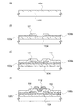
図1(A)は、半導体装置の有するトランジスタ100の上面図である。図1(B)は、図1(A)のA1−B1における断面図である。トランジスタ100は、基板102上に絶縁層104と、ソース電極層106aおよびドレイン電極層106bと、チャネル領域を形成する酸化物半導体層108と、ゲート絶縁層110と、ゲート電極層112を含む。
FIG. 1A is a top view of a
トランジスタ100は、ゲート電極層112がゲート絶縁層110を介して、酸化物半導体層108に重畳して形成されるトップゲート構造のトランジスタである。さらに、トランジスタ100は、酸化物半導体層108と絶縁層104との間にソース電極層106aおよびドレイン電極層106bを有するボトムコンタクト型である。
The
トランジスタ100は、トップゲート構造−ボトムコンタクト型のトランジスタであるため、絶縁層104の上面一部と酸化物半導体層108の下面一部が接する構造となる。それゆえ、トランジスタ100の作製工程において、絶縁層104に水素が多く存在する場合、酸化物半導体層108に水素が拡散する。酸化物半導体層108に水素が拡散することで、酸化物半導体層108内のキャリアが過剰となる。このため、トランジスタ100のしきい値電圧(Vth)が、マイナス方向に変動してしまい、ゲート電極に電圧が印加されていない状態(Vg=0V)においても、ドレイン電流が流れる(ノーマリーオン)。従って、絶縁層104に水素が多く存在する場合、トランジスタ100は電気特性が不良なトランジスタとなる。
Since the
酸化物半導体層108から拡散した水素を取り除くために、酸化物半導体層108を加熱処理する方法がある。しかし、トランジスタの作製工程を増やすほど、コストがかかり、歩留まりを悪くする可能性がある。
There is a method in which the
そこで、酸化物半導体層108と接する絶縁層104を、水素濃度が6×10²⁰atoms/cm3未満、好ましくは5×1020atoms/cm3以下、さらに好ましくは5×1019atoms/cm3以下である絶縁層とすることで、酸化物半導体層108に水素が拡散することを抑制でき、良好な電気特性を有するトランジスタを得ることができる。このようにすることで、トランジスタの作製工程を増やさずに、良好な電気特性を有するトランジスタを得ることができる。
Therefore, the
また、ゲート絶縁層110においても水素濃度が6×10²⁰atoms/cm3未満、好ましくは5×1020atoms/cm3以下、さらに好ましくは5×1019atoms/cm3以下とすることができる。つまり、絶縁層104およびゲート絶縁層110を水素濃度が6×1020atoms/cm3未満、好ましくは5×1020atoms/cm3以下、さらに好ましくは5×1019atoms/cm3以下とすることで、酸化物半導体層108に水素が拡散することを抑制できる。
In the
基板102としては、後の作製工程に耐えられるものであれば特に限定されない。例えば、基板102として、ガラス基板、セラミック基板、石英基板、若しくはサファイア基板などの絶縁性基板、シリコンなどの半導体材料でなる半導体基板、金属若しくはステンレスなどの導電体でなる導電性基板、または、半導体基板若しくは導電性基板の表面を絶縁材料で被覆した基板などを用いることができる。また、プラスチック基板も適宜用いることができる。
There is no particular limitation on the
また、ガラス基板としては、トランジスタの作製工程に加熱温度の高い加熱処理を行う場合には、歪点が730℃以上のものを用いるとよい。例えば、アルミノシリケートガラス、アルミノホウケイ酸ガラス、バリウムホウケイ酸ガラスなどのガラス材料が用いられている。一般に酸化ホウ素と比較して酸化バリウム(BaO)を多く含ませることで、より実用的な耐熱ガラスが得られる。このため、B2O3よりBaOを多く含むガラス基板を用いることが好ましい。 As the glass substrate, a substrate having a strain point of 730 ° C. or higher is preferably used when heat treatment is performed at a high heating temperature in the transistor manufacturing process. For example, glass materials such as aluminosilicate glass, aluminoborosilicate glass, and barium borosilicate glass are used. In general, a more practical heat-resistant glass can be obtained by containing more barium oxide (BaO) than boron oxide. For this reason, it is preferable to use a glass substrate containing more BaO than B 2 O 3 .
絶縁層104は、基板102からの不純物元素の拡散を防止する下地となる他に、トランジスタの作製工程におけるエッチング工程によって、基板がエッチングされることを防ぐ下地となる。絶縁層104の厚さに限定はないが、上記より、絶縁層104の厚さは50nm以上とすることが好ましい。
The insulating
絶縁層104には、酸化シリコン、酸化窒化シリコン、窒化酸化シリコン、酸化ハフニウム、酸化アルミニウム、または酸化タンタルなどの酸化物絶縁層を用いて、単層構造または2層以上の積層構造で形成する。また、積層構造とする際、例えば、基板102と接する絶縁層を窒化シリコンとし、酸化物半導体層108と接する絶縁層104を該酸化物絶縁層で形成すればよい。酸化物半導体層108と接する絶縁層104を、水素濃度が低減された酸化物絶縁層とすることで、酸化物半導体層108に水素の拡散を抑制する他に、酸化物半導体層108の欠陥に絶縁層104から酸素が供給されるため、トランジスタの電気特性が良好になる。この際、上記したように、絶縁層104の水素濃度は6×10²⁰atoms/cm3未満、好ましくは5×1020atoms/cm3以下、さらに好ましくは5×1019atoms/cm3以下とすることが必要である。
The insulating
ここで、酸化窒化シリコンとは、その組成において、窒素よりも酸素の含有量が多いものを示し、例として、少なくとも酸素が50原子%以上70原子%以下、窒素が0.5原子%以上15原子%以下、珪素が25原子%以上35原子%以下の範囲で含まれるものをいう。また、窒化酸化シリコンとは、その組成において、酸素よりも窒素の含有量が多いものを示し、例として、少なくとも酸素が5原子%以上30原子%以下、窒素が20原子%以上55原子%以下、珪素が25原子%以上35原子%以下の範囲で含まれるものをいう。但し、上記範囲は、ラザフォード後方散乱法(RBS:Rutherford Backscattering Spectrometry)や、水素前方散乱法(HFS:Hydrogen Forward Scattering)を用いて測定した場合のものである。また、構成元素の含有比率は、その合計が100原子%を超えない値をとる。 Here, silicon oxynitride indicates a composition having a higher oxygen content than nitrogen. For example, at least oxygen is 50 atomic% or more and 70 atomic% or less, and nitrogen is 0.5 atomic% or more and 15 or less. The atomic percent or less and silicon is contained in the range of 25 atomic percent to 35 atomic percent. In addition, silicon nitride oxide indicates a composition whose nitrogen content is higher than oxygen. For example, at least oxygen is 5 atomic% to 30 atomic%, and nitrogen is 20 atomic% to 55 atomic%. , Which includes silicon in a range of 25 atomic% to 35 atomic%. However, the above range is measured using Rutherford Backscattering Spectrometry (RBS) or Hydrogen Forward Scattering (HFS). Further, the content ratio of the constituent elements takes a value that the total does not exceed 100 atomic%.
本実施の形態では、絶縁層104にスパッタリング法で形成する酸化シリコン層を用いる場合と、絶縁層104にプラズマCVD(Plasma Enhanced Chemical Vapor Deposition)法で形成する酸化シリコン層を用いる場合について記載する。
In this embodiment, the case where a silicon oxide layer formed by a sputtering method is used for the insulating
スパッタリング法で絶縁層104を形成する場合、シリコン元素を含むターゲットを用いればよい。つまり、SiターゲットまたはSiO2ターゲットなどを用いることができる。得られる酸化シリコン層の水素濃度を低減させるため、好ましくは、SiO2ターゲットとし、より好ましくは、SiO2ターゲットに含まれる水酸基濃度が1000ppm以下、またはSIMS(Secondary Ion Mass Spectrometry)で測定した水素濃度が3.5×10¹⁹atoms/cm3以下であるSiO2ターゲットとすることである。さらに、形成する際に供給するガスは、アルゴン等の希ガスおよび、酸素とする。そして、形成する際に供給するガスは、水素、水、水酸基または水素化物などの不純物濃度がppm程度およびppb程度まで除去された高純度ガスを用いることが好ましい。
In the case where the insulating
スパッタリング法にはスパッタリング用電源に高周波電源を用いるRFスパッタリング法と、DCスパッタリング法があり、さらにパルス的にバイアスを与えるパルスDCスパッタリング法もある。 As the sputtering method, there are an RF sputtering method using a high-frequency power source as a sputtering power source and a DC sputtering method, and a pulse DC sputtering method for applying a bias in a pulsed manner.
また、材料の異なるターゲットを複数設置できる多元スパッタリング装置を用いて形成してもよい。多元スパッタリング装置は、同一チャンバーで異なる材料の膜を積層形成することや、同一チャンバーで複数種類の材料を同時に放電させて形成することもできる。 Alternatively, a multi-source sputtering apparatus in which a plurality of targets of different materials can be installed may be used. The multi-source sputtering apparatus can be formed by stacking films of different materials in the same chamber, or by simultaneously discharging a plurality of types of materials in the same chamber.
また、チャンバー内部に磁石機構を備えたマグネトロンスパッタリング法を用いるスパッタ装置や、グロー放電を使わずマイクロ波を用いて発生させたプラズマを用いるECRスパッタリング法を用いるスパッタリング装置がある。 Further, there are a sputtering apparatus using a magnetron sputtering method having a magnet mechanism inside a chamber, and a sputtering apparatus using an ECR sputtering method using plasma generated using microwaves without using glow discharge.
また、スパッタリング法として、ターゲット物質とスパッタガス成分とを化学反応させてそれらの化合物薄膜を形成するリアクティブスパッタリング法や、基板にも電圧をかけながら形成するバイアススパッタリング法を用いることもできる。 Further, as the sputtering method, a reactive sputtering method in which a target material and a sputtering gas component are chemically reacted to form a compound thin film thereof, or a bias sputtering method in which a substrate is formed while applying a voltage can be used.
本明細書のスパッタリングにおいては、基板を加熱しながらスパッタリングすることができ、上記したスパッタリング装置およびスパッタリング方法を適宜用いることができる。 Sputtering in this specification can be performed while heating the substrate, and the above-described sputtering apparatus and sputtering method can be used as appropriate.
このようにすることで、得られる酸化シリコン層の水素濃度を、6×10²⁰atoms/cm3未満、好ましくは5×1020atoms/cm3以下、さらに好ましくは5×1019atoms/cm3以下とすることができる。 By doing so, the hydrogen concentration of the obtained silicon oxide layer is less than 6 × 10 20 atoms / cm 3 , preferably 5 × 10 20 atoms / cm 3 or less, and more preferably 5 × 10 19 atoms / cm 3. It can be as follows.
絶縁層104の形成はスパッタリング法の他にプラズマCVD法を用いることができる。プラズマCVD法とは、プラズマCVD装置内の反応室に、原料となる堆積性ガスを供給し、プラズマエネルギーを援用して、膜を形成する方法である。
The insulating
プラズマCVD装置は、高周波電源を用いる容量結合型高周波プラズマCVD装置や、誘導結合型高周波プラズマCVD装置、マイクロ波発生源であるマグネトロンおよび誘電体を有し、マイクロ波を用いてプラズマを発生させるマイクロ波プラズマCVD装置(電子サイクロトロン共鳴プラズマCVD装置)その他、ヘリコン波プラズマCVD装置などがあり、本明細書中のプラズマCVD法においては、グロー放電プラズマを膜形成に利用するCVD装置を適宜用いることができる。また、プラズマCVD法においても、基板を加熱しながら行うことができる。 The plasma CVD apparatus includes a capacitively coupled high-frequency plasma CVD apparatus using a high-frequency power source, an inductively coupled high-frequency plasma CVD apparatus, a magnetron that is a microwave generation source, and a dielectric, and generates a plasma using microwaves. There are a wave plasma CVD apparatus (electron cyclotron resonance plasma CVD apparatus) and other helicon wave plasma CVD apparatuses. In the plasma CVD method in this specification, a CVD apparatus that uses glow discharge plasma for film formation is appropriately used. it can. Also, the plasma CVD method can be performed while heating the substrate.
水素濃度が低減した絶縁層104をプラズマCVD法で形成する場合、堆積性ガスとして分子構造に水素が含まれていないガスを選択する必要がある。
In the case where the insulating
つまり、堆積性ガスとしてSiH4ではなく、SiF4を使用する。さらに、堆積する膜を酸化物絶縁膜とするために水素や水の含有量が少ないN2OまたはO2の酸化ガスも使用する。また、プラズマCVD装置で発生するプラズマの広がりを考慮してその他添加するガス(アルゴンなどの希ガス)においても、水素や水の含有量が少ないガスとする。 That is, SiF 4 is used instead of SiH 4 as the deposition gas. Furthermore, in order to use the deposited film as an oxide insulating film, N 2 O or O 2 oxidizing gas having a low hydrogen or water content is also used. In addition, in consideration of the spread of the plasma generated in the plasma CVD apparatus, other gases to be added (rare gases such as argon) are made to have a low hydrogen or water content.
プラズマCVD法で絶縁層104となる酸化シリコン層を形成する際は、プラズマCVD装置の反応室内に残留している、または該反応室の内壁に吸着している水素や水などの不純物を除去したのち、上記ガスを用いて形成する。以上のようにすることで、プラズマCVD法を用いて形成する絶縁層104の水素濃度を6×10²⁰atoms/cm3未満、好ましくは5×1020atoms/cm3以下、さらに好ましくは5×1019atoms/cm3以下とすることができる。
When a silicon oxide layer to be the insulating
ソース電極層106aおよびドレイン電極層106bは絶縁層104上に形成される。ソース電極層106aおよびドレイン電極層106bの材料は、モリブデン、チタン、クロム、タンタル、タングステン、ネオジム、スカンジウム等の金属材料、これら金属材料を主成分とする合金材料を用いた導電膜、或いはこれら金属の窒化物を、単層でまたは積層で用いることができる。なお、後の工程において行われる加熱処理の温度に耐えうるのであれば、上記金属材料としてアルミニウム、銅を用いることもできる。アルミニウムまたは銅は、耐熱性や腐食性の問題を回避するために、高融点金属材料と組み合わせて用いるとよい。高融点金属材料としては、モリブデン、チタン、クロム、タンタル、タングステン、ネオジム、スカンジウム等を用いることができる。
The
例えば、ソース電極層106aおよびドレイン電極層106bとしては、アルミニウム膜上にモリブデン膜が積層された二層の積層構造、または銅膜上にモリブデン膜を積層した二層構造、または銅膜上に窒化チタン膜若しくは窒化タンタル膜を積層した二層構造、窒化チタン膜とモリブデン膜とを積層した二層構造、または銅−マグネシウム−アルミニウム合金膜上に銅膜を積層する二層構造とすることが好ましい。三層構造を有するソース電極層106aおよびドレイン電極層106bとしては、アルミニウム膜、アルミニウムとシリコンの合金膜、アルミニウムとチタンの合金膜またはアルミニウムとネオジムの合金膜を中間層とし、タングステン膜、窒化タングステン膜、窒化チタン膜またはチタン膜を上下層として積層した構造とすることが好ましい。
For example, as the
また、ソース電極層106aおよびドレイン電極層106bに、酸化インジウム、酸化インジウム酸化スズ合金、酸化インジウム酸化亜鉛合金、酸化亜鉛、酸化亜鉛アルミニウム、酸窒化亜鉛アルミニウム、または酸化亜鉛ガリウム等の透光性を有する酸化物導電膜を用いることができる。
The
ソース電極層106aおよびドレイン電極層106bの厚さは、特に限定はなく、ソース電極層106aおよびドレイン電極層106bとして機能する導電膜の電気抵抗や作製工程にかかる時間を考慮し、適宜決めることができる。例えば、10nm〜500nmで形成すればよい。
The thicknesses of the
チャネル領域を形成する酸化物半導体層108は、ソース電極層106aおよびドレイン電極層106bの上面一部と絶縁層104の上面一部と接して形成される。上記のように、絶縁層104は水素濃度が6×10²⁰atoms/cm3未満、好ましくは5×1020atoms/cm3以下、さらに好ましくは5×1019atoms/cm3以下であることから、酸化物半導体層108を形成する際に、酸化物半導体層108に水素が拡散することを抑制する。また酸化物半導体層108の厚さは、10nm〜300nm、好ましくは20nm〜100nmとする。
The
酸化物半導体層108は、In、Ga、およびZnを含むIn−Ga−Zn−O系非単結晶膜を用い、InMO3(ZnO)m(m>0)で表記される構造とする。なお、Mは、ガリウム(Ga)、鉄(Fe)、ニッケル(Ni)、マンガン(Mn)およびコバルト(Co)から選ばれた一の金属元素または複数の金属元素を示す。例えばMとして、Gaの場合があることの他、GaとNiまたはGaとFeなど、Ga以外の上記金属元素が含まれる場合がある。また、上記酸化物半導体において、Mとして含まれる金属元素の他に、不純物元素としてFe、Niその他の遷移金属元素、または該遷移金属の酸化物が含まれているものがある。そして、金属酸化物ターゲット中の金属酸化物の相対密度は80%以上、好ましくは95%以上、さらに好ましくは99.9%以上とする相対密度の高い金属酸化物ターゲットを用いる。
The
具体的には、四元系金属酸化物であるIn−Sn−Ga−Zn−O系や、三元系金属酸化物であるIn−Ga−Zn−O系、In−Sn−Zn−O系、In−Al−Zn−O系、Sn−Ga−Zn−O系、Al−Ga−Zn−O系、Sn−Al−Zn−O系や、二元系金属酸化物であるIn−Zn−O系、Sn−Zn−O系、Al−Zn−O系、Zn−Mg−O系、Sn−Mg−O系、In−Mg−O系や、In−O系、Sn−O系、Zn−O系などの酸化物半導体を用いて形成することができる。ここで、例えば、In−Ga−Zn−O系酸化物半導体とは、少なくともInとGaとZnとを含み、半導体特性を有する金属酸化物であり、その組成比は問わない。また、InとGaとZn以外の元素を含んでもよい。また、上記酸化物半導体に酸化シリコンを含んでもよい。 Specifically, an In—Sn—Ga—Zn—O system that is a quaternary metal oxide, an In—Ga—Zn—O system, or an In—Sn—Zn—O system that is a ternary metal oxide. In—Al—Zn—O, Sn—Ga—Zn—O, Al—Ga—Zn—O, Sn—Al—Zn—O, and In—Zn— which is a binary metal oxide O-based, Sn-Zn-O-based, Al-Zn-O-based, Zn-Mg-O-based, Sn-Mg-O-based, In-Mg-O-based, In-O-based, Sn-O-based, Zn It can be formed using an -O-based oxide semiconductor. Here, for example, an In—Ga—Zn—O-based oxide semiconductor is a metal oxide including at least In, Ga, and Zn and having semiconductor characteristics, and there is no limitation on the composition ratio thereof. Moreover, elements other than In, Ga, and Zn may be included. In addition, the oxide semiconductor may include silicon oxide.
ゲート絶縁層110は、ソース電極層106a、ドレイン電極層106bおよび、酸化物半導体層108を覆うように形成される。また、ゲート絶縁層110は、絶縁層104と同様に酸化物絶縁層で形成すればよい。ゲート絶縁層110の水素の含有量を低くすることで、良好な電気特性を有する半導体装置とすることができる。従って、酸化物半導体層と接するゲート絶縁層の水素濃度が6×10²⁰atoms/cm3未満、好ましくは5×1020atoms/cm3以下、さらに好ましくは5×1019atoms/cm3以下であることが好ましい。
The
ゲート電極112は、ゲート絶縁層110を介して、酸化物半導体層108に重畳して形成される。そして、ゲート電極112は、ソース電極層106aおよびドレイン電極層106bと同様の構成とすることができる。
The
なお、図1には示していないが、トランジスタ100上にパッシベーション層や層間絶縁層として機能する絶縁層を形成することが好ましい。
Note that although not illustrated in FIG. 1, an insulating layer functioning as a passivation layer or an interlayer insulating layer is preferably formed over the
以上より、絶縁層104またはゲート絶縁層110の一方または双方の水素濃度を6×10²⁰atoms/cm3未満、好ましくは5×1020atoms/cm3以下、さらに好ましくは5×1019atoms/cm3以下とすることで、酸化物半導体層108に水素が拡散することを抑制でき、良好な電気特性を有する半導体装置を得ることができる。
Accordingly, the hydrogen concentration of one or both of the insulating
なお、本実施の形態で示した構成は、本明細書の他の実施の形態および実施例で示す構成と適宜組み合わせることができる。 Note that the structure described in this embodiment can be combined as appropriate with any structure described in the other embodiments and examples of this specification.
(実施の形態2)
本実施の形態では、実施の形態1で示した半導体装置の作製方法について図2を用いて説明する。
(Embodiment 2)
In this embodiment, a method for manufacturing the semiconductor device described in Embodiment 1 will be described with reference to FIGS.
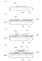
図2(A)に示したように、基板102上に絶縁層104を形成する。基板102および絶縁層104は実施の形態1に記載したものを用いることができ、本実施の形態では、基板102にガラス基板を用いる。絶縁層104は、ターゲットをSiO2とし、形成する際の供給するガスをアルゴン等の希ガスおよび、酸素として、RFスパッタリング法で酸化シリコン層を200nm形成する。
As shown in FIG. 2A, the insulating
また、実施の形態1で記載したが、絶縁層104をプラズマCVD法で形成する場合は、プラズマCVD装置内の反応室の内壁を加熱して、反応室の内壁から不純物を放出させ、反応室内に残留しているまたは反応室の内壁に吸着している不純物を除去した後、堆積性ガスとして、SiF4を、さらに、酸化させるためのガスとしてN2Oを、添加ガスとしてアルゴンを、反応室に供給し、プラズマエネルギーを援用して、絶縁層104を形成する。また、本実施の形態では、高周波電源を用いたプラズマCVD装置を用いる。
As described in Embodiment Mode 1, when the insulating
反応室内に残留しているまたは反応室の内壁に吸着している不純物を除去する方法として、排気工程や、三フッ化窒素などのフッ素化合物を用いたプラズマクリーニングを行うことが好ましい。 As a method for removing impurities remaining in the reaction chamber or adsorbed on the inner wall of the reaction chamber, it is preferable to perform an exhaust process or plasma cleaning using a fluorine compound such as nitrogen trifluoride.
次いで、ソース電極層106a、ドレイン電極層106bとして機能する導電膜を形成する。該導電膜として、本実施の形態では、チタンターゲットを用いたDCスパッタリング法で厚さ150nmのチタン膜を形成する。その後、第1のフォトリソグラフィ工程およびエッチング工程を行い、厚さ150nmのソース電極層106aおよびドレイン電極層106bを形成する。
Next, a conductive film functioning as the
該導電膜のエッチングには、ウェットエッチング、ドライエッチングのいずれを用いてもよい。なお、素子の微細化という観点からはドライエッチングを用いるのが好適である。エッチングガスやエッチング液については被エッチング材料に応じて適宜選択することができる。 Either wet etching or dry etching may be used for etching the conductive film. Note that dry etching is preferably used from the viewpoint of miniaturization of elements. An etching gas and an etchant can be appropriately selected according to the material to be etched.
なお、ソース電極層106aおよびドレイン電極層106bの側面はテーパ形状とすることが好ましい。ソース電極層106aおよびドレイン電極層106b上には、後の工程で酸化物半導体膜およびゲート電極となる導電膜を形成するので、段差の箇所における配線切れ防止のためである。ソース電極層106aおよびドレイン電極層106bの側面をテーパ形状とするためにはレジストマスクを後退させつつエッチングを行えばよい。
Note that side surfaces of the
そして、厚さ50nmの酸化物半導体膜を、DCスパッタリング法で形成する。該酸化物半導体膜は絶縁層104と接して形成されるため、絶縁層104から、該酸化物半導体膜の欠陥に酸素が供給される。その後、第2のフォトリソグラフィ工程およびエッチング工程を行い、島状に加工された酸化物半導体層107を形成する。本実施の形態では、DCスパッタリング法を用いるが、真空蒸着法、パルスレーザ堆積法、CVD法などを用いて形成してもよい。
Then, an oxide semiconductor film with a thickness of 50 nm is formed by a DC sputtering method. Since the oxide semiconductor film is formed in contact with the insulating
酸化物半導体膜は、実施の形態1で説明した酸化物半導体を用いることができる。本実施の形態では、In(インジウム)、Ga(ガリウム)、およびZn(亜鉛)を含む酸化物半導体ターゲット(モル数比がIn2O3:Ga2O3:ZnO=1:1:1、In2O3:Ga2O3:ZnO=1:1:2)を用いて、スパッタリング法により、厚さ50nmのIn−Ga−Zn−O系非単結晶膜を形成する。さらに、本実施の形態では、DCスパッタリング法を用い、アルゴンの流量30sccmとし、酸素の流量15sccmとし、基板温度は室温(15℃から35℃)とする。 As the oxide semiconductor film, the oxide semiconductor described in Embodiment 1 can be used. In this embodiment, an oxide semiconductor target including In (indium), Ga (gallium), and Zn (zinc) (the molar ratio is In 2 O 3 : Ga 2 O 3 : ZnO = 1: 1: 1, An In—Ga—Zn—O-based non-single-crystal film with a thickness of 50 nm is formed by a sputtering method using In 2 O 3 : Ga 2 O 3 : ZnO = 1: 1: 2. Further, in this embodiment mode, a DC sputtering method is used, the argon flow rate is 30 sccm, the oxygen flow rate is 15 sccm, and the substrate temperature is room temperature (15 ° C. to 35 ° C.).
また、酸化物半導体膜として、In−Zn−O系の酸化物半導体を用いる場合、用いるターゲットの組成比は、原子数比で、In:Zn=50:1〜1:2(モル数比に換算するとIn2O3:ZnO=25:1〜1:4)、好ましくはIn:Zn=20:1〜1:1(モル数比に換算するとIn2O3:ZnO=10:1〜1:2)、さらに好ましくはIn:Zn=15:1〜3:2(モル数比に換算するとIn2O3:ZnO=15:2〜3:4)とする。例えば、In−Zn−O系酸化物半導体の形成に用いるターゲットは、原子数比がIn:Zn:O=X:Y:Zのとき、Z>1.5X+Yとする。 In the case where an In—Zn—O-based oxide semiconductor is used as the oxide semiconductor film, the composition ratio of the target used is an atomic ratio, and In: Zn = 50: 1 to 1: 2 (molar ratio). When converted, In 2 O 3 : ZnO = 25: 1 to 1: 4), preferably In: Zn = 20: 1 to 1: 1 (in terms of molar ratio, In 2 O 3 : ZnO = 10: 1 to 1). : 2), more preferably In: Zn = 15: 1 to 3: 2 (in terms of molar ratio, In 2 O 3 : ZnO = 15: 2 to 3: 4). For example, a target used for forming an In—Zn—O-based oxide semiconductor satisfies Z> 1.5X + Y when the atomic ratio is In: Zn: O = X: Y: Z.
なお、酸化物半導体膜をスパッタリング法により形成する前に、アルゴンガスを導入してプラズマを発生させる逆スパッタを行うことが好ましい。逆スパッタとは、アルゴン雰囲気下で基板にRF電源を用いて電圧を印加して基板近傍にプラズマを形成して表面を改質する方法である。なお、アルゴン雰囲気に代えて窒素、ヘリウムなどを用いてもよい。また、アルゴン雰囲気に酸素、亜酸化窒素などを加えた雰囲気で行ってもよい。また、アルゴン雰囲気に塩素、四フッ化炭素などを加えた雰囲気で行ってもよい。 Note that before the oxide semiconductor film is formed by a sputtering method, reverse sputtering in which argon gas is introduced to generate plasma is preferably performed. Reverse sputtering is a method of modifying the surface by forming a plasma near the substrate by applying a voltage to the substrate using an RF power supply in an argon atmosphere. Note that nitrogen, helium, or the like may be used instead of the argon atmosphere. Alternatively, an argon atmosphere may be used in which oxygen, nitrous oxide, or the like is added. Alternatively, the reaction may be performed in an atmosphere in which chlorine, carbon tetrafluoride, or the like is added to an argon atmosphere.
酸化物半導体膜の形成の際には、例えば、減圧状態に保持された処理室内に基板を保持し、基板の温度が100℃以上550℃未満、好ましくは200℃以上400℃以下となるように基板を熱する。または、酸化物半導体膜の形成の際の基板の温度は、室温(15℃から35℃)としてもよい。そして、処理室内の水分を除去しつつ、水素や水などが除去されたスパッタガスを導入し、酸化物半導体ターゲットを用いて酸化物半導体膜を形成する。基板を熱しながら酸化物半導体膜を形成することにより、酸化物半導体膜に含まれる不純物を低減することができる。また、スパッタによる損傷を軽減することができる。処理室内の水分を除去するためには、吸着型の真空ポンプを用いることが好ましい。例えば、クライオポンプ、イオンポンプ、チタンサブリメーションポンプなどを用いることができる。また、ターボポンプにコールドトラップを加えたものを用いてもよい。クライオポンプなどを用いて排気することで、処理室から水素や水などを除去することができるため、酸化物半導体膜中の不純物濃度を低減できる。 When forming the oxide semiconductor film, for example, the substrate is held in a treatment chamber kept under reduced pressure so that the temperature of the substrate is 100 ° C. or higher and lower than 550 ° C., preferably 200 ° C. or higher and 400 ° C. or lower. Heat the substrate. Alternatively, the temperature of the substrate in forming the oxide semiconductor film may be room temperature (15 ° C. to 35 ° C.). Then, a sputtering gas from which hydrogen, water, or the like is removed is introduced while moisture in the treatment chamber is removed, and an oxide semiconductor film is formed using an oxide semiconductor target. By forming the oxide semiconductor film while the substrate is heated, impurities contained in the oxide semiconductor film can be reduced. Further, damage due to sputtering can be reduced. In order to remove moisture in the processing chamber, an adsorption-type vacuum pump is preferably used. For example, a cryopump, an ion pump, a titanium sublimation pump, or the like can be used. Further, a turbo pump provided with a cold trap may be used. By exhausting using a cryopump or the like, hydrogen, water, or the like can be removed from the treatment chamber, so that the impurity concentration in the oxide semiconductor film can be reduced.
ここまでの工程で得られた構成を図2(B)に示す。 The structure obtained through the steps up to here is illustrated in FIG.
次いで、大気雰囲気または不活性ガス雰囲気(窒素、またはヘリウム、ネオン、アルゴン等)下、或いは大気圧下の露点がマイナス60℃以下の、水分含有量が少ない空気下において、酸化物半導体層107に加熱処理を施してもよい。具体的には、大気雰囲気下において、100℃以上400℃以下で、10分間以上、好ましくは350℃、60分間の加熱処理で行うことである。本実施の形態では、酸化物半導体層107に加熱処理を施すことで、水分、水素が脱離した酸化物半導体層108が形成される。この際、絶縁層104から、酸化物半導体層108の欠陥に酸素が供給される。
Next, the
また、不活性ガス雰囲気(窒素、またはヘリウム、ネオン、アルゴン等)下において、500℃以上750℃以下(若しくはガラス基板の歪点以下の温度)で1分間以上10分間以下程度、好ましくは600℃、3分間以上6分間以下程度のRTA(Rapid Thermal Anneal)処理で行うことができる。RTA法を用いれば、短時間に脱水化または脱水素化が行えるため、ガラス基板の歪点を超える温度でも処理することができる。なお、加熱処理においては、不活性ガス(窒素、またはヘリウム、ネオン、アルゴン等の希ガス)に、水分、水素などが含まれないことが好ましい。または、加熱処理装置に導入する窒素、またはヘリウム、ネオン、アルゴン等の希ガスの純度を、6N(99.9999%)以上、好ましくは7N(99.99999%)以上、(即ち不純物濃度を1ppm以下、好ましくは0.1ppm以下)とすることが好ましい。 In an inert gas atmosphere (nitrogen, helium, neon, argon, or the like), the temperature is 500 ° C. or higher and 750 ° C. or lower (or the temperature below the strain point of the glass substrate) for 1 minute or longer and 10 minutes or shorter, preferably 600 ° C. It can be performed by RTA (Rapid Thermal Annealing) treatment for about 3 minutes to 6 minutes. When the RTA method is used, dehydration or dehydrogenation can be performed in a short time, so that the treatment can be performed even at a temperature exceeding the strain point of the glass substrate. Note that in the heat treatment, it is preferable that moisture, hydrogen, and the like be not contained in the inert gas (nitrogen or a rare gas such as helium, neon, or argon). Alternatively, the purity of nitrogen or a rare gas such as helium, neon, or argon introduced into the heat treatment apparatus is 6N (99.9999%) or more, preferably 7N (99.99999%) or more (that is, the impurity concentration is 1 ppm). Or less, preferably 0.1 ppm or less).
なお、上記加熱処理は、島状の酸化物半導体層108形成後のタイミングに限らず、島状の酸化物半導体層108形成前の酸化物半導体膜に対して行ってもよい。また、上記加熱処理を、酸化物半導体膜107形成後に複数回行ってもよい。
Note that the above heat treatment is not limited to the timing after the island-shaped
本実施の形態では、大気雰囲気下において、基板温度が設定温度の350℃に達した状態で60分間、加熱処理を行う。加熱処理は、電気炉を用いた加熱方法、加熱した気体を用いるGRTA(Gas Rapid Thermal Anneal)法またはランプ光を用いるLRTA(Lamp Rapid Thermal Anneal)法などの瞬間加熱方法などを用いることができる。例えば、電気炉を用いて加熱処理を行う場合、昇温特性を0.1℃/min以上20℃/min以下、降温特性を0.1℃/min以上15℃/min以下とすることが好ましい。 In this embodiment, heat treatment is performed for 60 minutes in an air atmosphere in a state where the substrate temperature has reached a set temperature of 350 ° C. For the heat treatment, a heating method using an electric furnace, an instantaneous heating method such as a GRTA (Gas Rapid Thermal Anneal) method using a heated gas, or an LRTA (Lamp Rapid Thermal Anneal) method using lamp light can be used. For example, when heat treatment is performed using an electric furnace, it is preferable that the temperature rise characteristic is 0.1 ° C./min to 20 ° C./min and the temperature drop characteristic is 0.1 ° C./min to 15 ° C./min. .
不活性ガス雰囲気下における加熱処理後の、島状の酸化物半導体層108は、非晶質であることが好ましいが、一部結晶化していてもよい。
The island-shaped
ここで、酸化物半導体層108の露出した表面に、酸素、オゾン、一酸化二窒素を用いて、プラズマ処理を施してもよい。プラズマ処理をすることで、酸化物半導体層108の欠陥に酸素を供給することができる。
Here, plasma treatment may be performed on the exposed surface of the
次いで、ゲート絶縁層110を形成する。ゲート絶縁層110は、絶縁層104と同様にして形成することができる。本実施の形態では、ターゲットをSiO2とし、形成する際に供給するガスをアルゴン等の希ガスおよび、酸素として、RFスパッタリング法で酸化シリコン層を200nm形成する。
Next, the
ここまでの工程で得られた構成を図2(C)に示す。 The structure obtained through the steps up to here is illustrated in FIG.
なお、ゲート絶縁層110を形成した後に、加熱処理を施してもよい。加熱処理は大気雰囲気下、または不活性ガス雰囲気(窒素、またはヘリウム、ネオン、アルゴン等)下において行う。好ましくは200℃以上400℃以下で行うこととし、本実施の形態では、大気雰囲気下で350℃、1時間の加熱処理を行う。または、ゲート絶縁層110を形成する前に行った先の加熱処理と同様に、高温短時間のRTA処理を行ってもよい。この加熱処理を行うタイミングは、ゲート絶縁層110の形成後であれば特に限定されず、他の工程、例えば透明導電膜を低抵抗化させるための加熱処理と兼ねることで、工程数を増やすことなく行うことができる。
Note that heat treatment may be performed after the
ゲート絶縁層110の上に、ゲート電極層112として機能する導電膜を形成し、第3のフォトリソグラフィ工程およびエッチング工程を行い、ゲート電極層112を形成する。該導電膜は、ソース電極層106aおよびドレイン電極層106bと同様の構成とすることができる。本実施の形態では、チタンターゲットを用いたDCスパッタリング法で厚さ150nmのチタン膜を形成し、第3のフォトリソグラフィ工程およびエッチング工程により、ゲート電極層112を形成した。
A conductive film functioning as the
ここまでの工程を経て得られた構成を図2(D)に示す。 A structure obtained through the steps up to here is illustrated in FIG.
以上により、実施の形態1で示した半導体装置を作製することができる。 Through the above steps, the semiconductor device described in Embodiment 1 can be manufactured.
なお、本実施の形態で示した構成は、本明細書の他の実施の形態および実施例で示す構成と適宜組み合わせることができる。 Note that the structure described in this embodiment can be combined as appropriate with any structure described in the other embodiments and examples of this specification.
(実施の形態3)
本実施の形態では、本発明の別の一態様である半導体装置について図3を用いて説明する。
(Embodiment 3)
In this embodiment, a semiconductor device which is another embodiment of the present invention will be described with reference to FIGS.
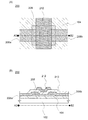
図3(A)は、半導体装置の有するトランジスタ200の上面図である。図3(B)は、図3(A)のA2−B2における断面図である。トランジスタ200は、基板102上に絶縁層104と、チャネル領域を形成する酸化物半導体層208と、ソース電極層206aおよびドレイン電極層206bと、ゲート絶縁層210と、ゲート電極層212を含む。
FIG. 3A is a top view of the
トランジスタ200は、ゲート電極層212がゲート絶縁層210を介して、酸化物半導体層208に重畳して形成されるトップゲート構造のトランジスタである。さらに、トランジスタ200は、ソース電極層206aおよびドレイン電極層206bと絶縁層104との間に、酸化物半導体層208を有するトップコンタクト型である。
The
トランジスタ200は、上記トップゲート構造−トップコンタクト型のトランジスタであるため、絶縁層104の上面一部と酸化物半導体層208下面一部が接する構造となる。それゆえ、トランジスタ200の作製工程において、絶縁層104に水素が多く存在する場合、酸化物半導体層208に水素が拡散する。酸化物半導体層208に水素が拡散することで、酸化物半導体層208内のキャリアが過剰となる。このため、トランジスタ200のしきい値電圧が、マイナス方向に変動してしまい、ゲート電極に電圧が印加されていない状態(Vg=0V)においても、ドレイン電流が流れる(ノーマリーオン)ため、電気特性が不良なトランジスタとなる。
Since the
酸化物半導体層208から拡散した水素を取り除くために、酸化物半導体層208を加熱処理する方法がある。しかし、トランジスタの作製工程を増やすほど、コストがかかり、歩留まりを悪くする可能性がある。
In order to remove hydrogen diffused from the
そこで、酸化物半導体層208と接する絶縁層104を、水素濃度が6×10²⁰atoms/cm3未満、好ましくは5×1020atoms/cm3以下、さらに好ましくは5×1019atoms/cm3以下である絶縁層とすることで、酸化物半導体層208に水素が拡散することを抑制でき、良好な電気特性を有するトランジスタを得ることができる。この方法にすることで、トランジスタの作製工程を増やさずに、良好な電気特性を有するトランジスタを得ることができる。
Therefore, the insulating
また、ゲート絶縁層210においても水素濃度が6×10²⁰atoms/cm3未満、好ましくは5×1020atoms/cm3以下、さらに好ましくは5×1019atoms/cm3以下とすることができる。つまり、絶縁層104およびゲート絶縁層210の水素濃度が6×1020atoms/cm3未満、好ましくは5×1020atoms/cm3以下、さらに好ましくは5×1019atoms/cm3以下とすることで、酸化物半導体層208に水素が拡散することを抑制できる。
In the
基板102は、実施の形態1の説明と同様である。
The
絶縁層104は、実施の形態1で説明した同様の構成からなる同様のものとすることができる。絶縁層104は、基板102からの不純物元素の拡散を防止する下地となる他に、トランジスタの作製工程におけるエッチング工程によって、基板がエッチングされることを防ぐ下地となる。それゆえ、絶縁層104の厚さは50nm以上とすることが好ましい。
The insulating
絶縁層104には、酸化シリコン、酸化窒化シリコン、窒化シリコン、窒化酸化シリコン、酸化ハフニウム、酸化アルミニウム、または酸化タンタルなどの酸化物絶縁層を用いて、単層構造または2層以上の積層構造で形成する。また、2層以上の積層構造とする際に、基板102と接する絶縁層を窒化シリコン層とし、酸化物半導体層208と接する絶縁層104を上記したもので形成してもよい。酸化物半導体層208と接する絶縁層104を、水素濃度が低減された酸化物絶縁層とすることで、酸化物半導体層208の欠陥に、絶縁層104から酸素が供給されるため、トランジスタの電気特性が良好になる。この際、上記したように、水素濃度が6×10²⁰atoms/cm3未満、好ましくは5×1020atoms/cm3以下、さらに好ましくは5×1019atoms/cm3以下である絶縁層104とすることが必要である。
The insulating
そして、本実施の形態における絶縁層104は、実施の形態1で示したように、スパッタリング法で形成する酸化シリコン層または、プラズマCVD法で形成する酸化シリコン層を用いることができる。
As the insulating
スパッタリング法で絶縁層104を形成する場合、シリコン元素を含むターゲットを用いればよい。つまり、SiターゲットまたはSiO2ターゲットなどを用いることができる。
得られる酸化シリコン層の水素濃度を低減させるため、好ましくは、SiO2ターゲットとし、より好ましくは、SiO2ターゲットに含まれる水酸基濃度が1000ppm以下、またはSIMSで測定した水素濃度が3.5×10¹⁹atoms/cm3以下であるSiO2ターゲットとすることである。さらに、形成する際に供給するガスはアルゴン等の希ガスおよび、酸素とする。そして、該形成する際に供給するガスは、水素、水、水酸基または水素化物などの不純物濃度がppm程度、またはppb程度まで除去された高純度ガスを用いることが好ましい。
In the case where the insulating
In order to reduce the hydrogen concentration of the obtained silicon oxide layer, it is preferably an SiO 2 target, more preferably, the hydroxyl concentration contained in the SiO 2 target is 1000 ppm or less, or the hydrogen concentration measured by SIMS is 3.5 × 10. The SiO 2 target is 19 atoms / cm 3 or less. Further, a gas supplied at the time of formation is a rare gas such as argon and oxygen. The gas supplied at the time of formation is preferably a high-purity gas from which impurities such as hydrogen, water, hydroxyl group or hydride have been removed to a concentration of about ppm or ppb.
絶縁層104をスパッタリング法で形成する代わりに、プラズマCVD法を用いることができる。プラズマCVD法とは、プラズマCVD装置内の反応室に、原料となる堆積性ガスを供給し、プラズマエネルギーを援用して、膜を形成する方法である。
Instead of forming the insulating
プラズマCVD法で酸化シリコン層を形成する際には、堆積性ガスとして分子構造に水素が含まれていないガスを選択し、形成する必要がある。 When a silicon oxide layer is formed by a plasma CVD method, it is necessary to select and form a gas that does not contain hydrogen in the molecular structure as a deposition gas.
堆積性ガスとしてSiH4ではなく、SiF4を使用する。さらに、酸化させるためのガスについて、水素や水の含有量が少ないN2OまたはO2とし、プラズマの広がりを考慮してアルゴンなどその他に添加するガスにおいても、水素や水の含有量が少ないガスとする。 SiF 4 is used instead of SiH 4 as the deposition gas. Further, the gas to be oxidized is N 2 O or O 2 having a small content of hydrogen or water, and a gas having a small content of hydrogen or water is added to other gases such as argon in consideration of the spread of plasma. And
さらに、プラズマCVD法で酸化シリコン層を形成する際に、プラズマCVD装置の反応室内に残留しているまたは反応室の内壁に吸着している水素や水などの不純物を除去したのち、上記構成のガスを用いて形成する。以上のようにすることで、プラズマCVD法を用いた絶縁層104の水素濃度を6×10²⁰atoms/cm3未満、好ましくは5×1020atoms/cm3以下、さらに好ましくは5×1019atoms/cm3以下とすることができる。
Further, when the silicon oxide layer is formed by plasma CVD, impurities such as hydrogen and water remaining in the reaction chamber of the plasma CVD apparatus or adsorbed on the inner wall of the reaction chamber are removed, and Form using gas. Thus, the hydrogen concentration of the insulating
チャネル領域を形成する酸化物半導体層208は、絶縁層104上に形成される。酸化物半導体層208は実施の形態1の酸化物半導体層108と同様である。実施の形態1に記載したように、絶縁層104は水素濃度が6×10²⁰atoms/cm3未満、好ましくは5×1020atoms/cm3以下、さらに好ましくは5×1019atoms/cm3以下であることから、酸化物半導体層208を形成する際に、酸化物半導体層208に水素が拡散することを抑制する。
An
ゲート絶縁層210は、ソース電極層206a、ドレイン電極層206bおよび、酸化物半導体層208を覆うように形成される。ゲート絶縁層210は、実施の形態1のゲート絶縁層110と同様である。さらに、ゲート絶縁層210は、絶縁層104と同様に水素の含有量が少ない酸化物絶縁層を用いることで、良好な電気特性を有する半導体装置とすることができるため、酸化物半導体層と接するゲート絶縁層の水素濃度が6×10²⁰atoms/cm3未満、好ましくは5×1020atoms/cm3以下、さらに好ましくは5×1019atoms/cm3以下であることが好ましい。
The
ソース電極206aおよびドレイン電極206bは絶縁層104上面一部および、酸化物半導体層208の上面一部に形成される。ソース電極層206aおよびドレイン電極層206bは、実施の形態1のソース電極層106aおよびドレイン電極層106bと同様である。
The source electrode 206 a and the
ゲート電極212は、ゲート絶縁層210を介して、酸化物半導体層208に重畳して形成される。そして、ゲート電極212は、実施の形態1のゲート電極112と同様である。
The
なお、図3には示していないが、トランジスタ200上にパッシベーション層や層間絶縁層として機能する絶縁層を形成することができる。
Note that although not illustrated in FIG. 3, an insulating layer functioning as a passivation layer or an interlayer insulating layer can be formed over the
以上により、絶縁層104または、絶縁層104およびゲート絶縁層210の水素濃度を6×10²⁰atoms/cm3未満、好ましくは5×1020atoms/cm3以下、さらに好ましくは5×1019atoms/cm3以下とすることで、酸化物半導体層208に水素が拡散することを抑制でき、良好な電気特性を有する半導体装置を得ることができる。
Accordingly, the hydrogen concentration of the insulating
なお、本実施の形態で示した構成は、本明細書の他の実施の形態および実施例で示す構成と適宜組み合わせることができる。 Note that the structure described in this embodiment can be combined as appropriate with any structure described in the other embodiments and examples of this specification.
(実施の形態4)
本実施の形態では、実施の形態3に記載した半導体装置の作製方法について図4を用いて説明する。
(Embodiment 4)
In this embodiment, a method for manufacturing the semiconductor device described in
図4(A)に示したように、基板102上に絶縁層104を形成する。基板102および絶縁層104は実施の形態3に記載したものを用いることができ、本実施の形態では、基板102にガラス基板を用いる。絶縁層104は、ターゲットをSiO2とし、形成する際の供給するガスにアルゴン等の希ガスおよび、酸素として、RFスパッタリング法で酸化シリコン層を200nm形成する。
As shown in FIG. 4A, the insulating
また、絶縁層104をプラズマCVD法で形成する場合は、実施の形態2で記載したようにして形成すればよい。
In the case where the insulating
そして、厚さ50nmの酸化物半導体膜を、スパッタリング法で成膜する。絶縁層104と接して形成されるため、絶縁層104から、酸化物半導体膜の欠陥に酸素が供給される。その後、第1のフォトリソグラフィ工程およびエッチング工程を行い、島状に加工された酸化物半導体層207を形成する。
Then, an oxide semiconductor film with a thickness of 50 nm is formed by a sputtering method. Since it is formed in contact with the insulating
酸化物半導体膜は、実施の形態2に記載したようにして形成すればよい。 The oxide semiconductor film may be formed as described in Embodiment 2.
ここまでの工程で得られた構成を図4(A)に示す。 The structure obtained through the steps up to here is illustrated in FIG.
次いで、ソース電極層206a、ドレイン電極層206bとして機能する導電膜を成膜する。該導電膜として、本実施の形態では、実施の形態2と同様に、チタンターゲットを用いたDCスパッタリング法で厚さ150nmのチタン膜を成膜する。その後、第2のフォトリソグラフィ工程およびエッチング工程を行い、厚さ150nmのソース電極層206aおよびドレイン電極層206bを形成した。
Next, a conductive film functioning as the
該導電膜のエッチングには、実施の形態2で説明した同様の方法を用いることが出来る。 For the etching of the conductive film, the same method described in Embodiment 2 can be used.
次いで、実施の形態2で説明したように、大気雰囲気または不活性ガス雰囲気(窒素、またはヘリウム、ネオン、アルゴン等)下、或いは大気圧下の露点がマイナス60℃以下の、水分含有量が少ない空気下において、酸化物半導体層207に加熱処理を施してもよい。具体的には、大気雰囲気下において、100℃以上400℃以下、で10分間以上、好ましくは350℃、60分間の加熱処理で行うことである。本実施の形態では、酸化物半導体層207に加熱処理を施すことで、水分、水素が脱離した酸化物半導体層208が形成される。この際、絶縁層104から、酸化物半導体層208の欠陥に酸素が供給される。
Next, as described in Embodiment 2, the dew point is −60 ° C. or less under an air atmosphere or an inert gas atmosphere (nitrogen, helium, neon, argon, etc.) or atmospheric pressure, and the water content is low. The
なお、上記加熱処理は、ソース電極層206a、ドレイン電極層206b形成後のタイミングに限らず、ソース電極層206a、ドレイン電極層206b形成前の、第1のフォトリソグラフィ工程およびエッチング工程により形成した島状の酸化物半導体層207に対して行ってもよい。また、上記加熱処理を、酸化物半導体層207形成後に複数回行ってもよい。
Note that the above heat treatment is not limited to the timing after the
本実施の形態では、大気雰囲気下において、350℃、基板温度が上記設定温度に達した状態で60分間、加熱処理を行う。本実施の形態における加熱処理の詳細は、実施の形態2と同様である。ここまでの工程で得られた構成を図4(B)に示す。 In this embodiment, heat treatment is performed for 60 minutes at 350 ° C. in a state where the substrate temperature has reached the set temperature in an air atmosphere. The details of the heat treatment in this embodiment are the same as those in Embodiment 2. The structure obtained through the steps up to here is illustrated in FIG.
ここで、酸化物半導体層208の露出した表面に、酸素、オゾン、一酸化二窒素を用いて、プラズマ処理を施してもよい。プラズマ処理をすることで、酸化物半導体層208の欠陥に酸素を供給することができる。
Here, plasma treatment may be performed on the exposed surface of the
次いで、ゲート絶縁層210を形成する。ゲート絶縁層210は、絶縁層104と同様にして出来る。本実施の形態では、実施の形態2と同様にターゲットをSiO2とし、形成する際の雰囲気ガスにアルゴン等の希ガスおよび、酸素として、RFスパッタリング法で酸化シリコン層を200nm形成する。
Next, the
ここまでの工程で得られた構成を図4(C)に示す。 The structure obtained through the steps up to here is illustrated in FIG.
なお、ゲート絶縁層210を形成した後に、加熱処理を施してもよい。本加熱処理の方法や加熱処理を行うタイミングは実施の形態2に記述した通りである。
Note that heat treatment may be performed after the
ゲート絶縁層210の上に、ゲート電極層212として機能する導電膜を成膜し、第3のフォトリソグラフィ工程およびエッチング工程を行い、ゲート電極層212を形成する。該導電膜は、ソース電極層206aおよびドレイン電極層206bと同様の構成とすることができる。本実施の形態では、実施の形態2と同様にチタンターゲットを用いたDCスパッタリング法で厚さ150nmのチタン膜を成膜し、第3のフォトリソグラフィ工程およびエッチング工程により、ゲート電極層212を形成する。
A conductive film functioning as the
ここまでの工程を経て得られた構成を図4(D)に示す。 A structure obtained through the steps up to here is illustrated in FIG.
以上により、実施の形態3で示した半導体装置を作製することができる。
Through the above steps, the semiconductor device described in
なお、本実施の形態で示した構成は、本明細書の他の実施の形態および実施例で示す構成と適宜組み合わせることができる。 Note that the structure described in this embodiment can be combined as appropriate with any structure described in the other embodiments and examples of this specification.
(実施の形態5)
上記実施の形態で説明したトランジスタを作製し、該トランジスタを画素部、さらには駆動回路に用いて表示機能を有する半導体装置(表示装置ともいう)を作製することができる。また、トランジスタを用いた駆動回路の一部または全体を、画素部と同じ基板上に一体形成し、システムオンパネルを形成することができる。また、上記実施の形態で記載した酸化物半導体を用いたトランジスタで、メモリセルを含んだ半導体装置を作製することもできる。
(Embodiment 5)
The transistor described in any of the above embodiments can be manufactured, and a semiconductor device (also referred to as a display device) having a display function can be manufactured using the transistor in a pixel portion and further in a driver circuit. In addition, part or the whole of a driver circuit using a transistor can be formed over the same substrate as the pixel portion to form a system-on-panel. In addition, a semiconductor device including a memory cell can be manufactured using the transistor including the oxide semiconductor described in the above embodiment.
表示装置は表示素子を含む。表示素子としては液晶素子(液晶表示素子ともいう)、発光素子(発光表示素子ともいう)を用いることができる。発光素子は、電流または電圧によって輝度が制御される素子をその範疇に含んでおり、具体的には無機EL(Electro Luminescence)、有機EL等が含まれる。また、電子インクなど、電気的作用によりコントラストが変化する表示媒体も適用することができる。 The display device includes a display element. As the display element, a liquid crystal element (also referred to as a liquid crystal display element) or a light-emitting element (also referred to as a light-emitting display element) can be used. The light-emitting element includes, in its category, an element whose luminance is controlled by current or voltage, and specifically includes inorganic EL (Electro Luminescence), organic EL, and the like. In addition, a display medium whose contrast is changed by an electric effect, such as electronic ink, can be used.
また、表示装置は、表示素子が封止された状態にあるパネルと、該パネルにコントローラを含むIC等を実装した状態にあるモジュールとを含む。さらに、該表示装置を作製する過程における、表示素子が完成する前の一形態に相当する素子基板に関し、該素子基板は、電流を表示素子に供給するための手段を複数の各画素に備える。素子基板は、具体的には、表示素子の画素電極のみが形成された状態であってもよいし、画素電極となる導電膜を形成した後であって、エッチングして画素電極を形成する前の状態であってもよいし、あらゆる形態があてはまる。 The display device includes a panel in which the display element is sealed, and a module in which an IC including a controller is mounted on the panel. Further, in the process of manufacturing the display device, the element substrate which corresponds to one embodiment before the display element is completed is provided with a means for supplying current to the display element in each of the plurality of pixels. Specifically, the element substrate may be in a state where only the pixel electrode of the display element is formed, or after the conductive film to be the pixel electrode is formed and before the pixel electrode is formed by etching. Or any form.
なお、本明細書中における表示装置とは、画像表示デバイス、表示デバイス、もしくは光源(照明装置含む)を指す。また、コネクター、例えばFPC(Flexible printed circuit)もしくはTAB(Tape Automated Bonding)テープもしくはTCP(Tape Carrier Package)が取り付けられたモジュール、TABテープやTCPの先にプリント配線板が設けられたモジュール、または表示素子にCOG(Chip On Glass)方式によりIC(集積回路)が直接実装されたモジュールも全て表示装置に含むものとする。 Note that a display device in this specification means an image display device, a display device, or a light source (including a lighting device). Also, a connector, for example, a module with a FPC (Flexible printed circuit) or TAB (Tape Automated Bonding) tape or TCP (Tape Carrier Package), a module with a printed wiring board at the end of a TAB tape or TCP, or a display It is assumed that the display device includes all modules in which an IC (integrated circuit) is directly mounted on the element by a COG (Chip On Glass) method.
(実施の形態6)
上記実施の形態で説明したトランジスタを用いた表示装置は、電子インクを駆動させて表示する電子ペーパーに適用することができる。電子ペーパーは、情報を表示するものであればあらゆる分野の電子機器に用いることが可能である。例えば、電子ペーパーを用いて、電子書籍(電子ブック)、ポスター、デジタルサイネージ、PID(Public Information Display)、電車などの乗り物の車内広告、クレジットカード等の各種カードにおける表示等に適用することができる。電子機器の一例を図5に示す。
(Embodiment 6)
The display device including the transistor described in any of the above embodiments can be applied to electronic paper that is displayed by driving electronic ink. Electronic paper can be used for electronic devices in various fields as long as they display information. For example, it can be applied to electronic books (electronic books), posters, digital signage, PID (Public Information Display), advertisements in vehicles such as trains, displays on various cards such as credit cards, etc. using electronic paper. . An example of the electronic device is illustrated in FIG.
図5は、電子機器の一例として電子書籍2700を示している。例えば、電子書籍2700は、筐体2701および筐体2703の2つの筐体で構成されている。筐体2701および筐体2703は、軸部2711により一体とされており、該軸部2711を軸として開閉動作を行うことができる。このような構成により、紙の書籍のような動作を行うことが可能となる。
FIG. 5 illustrates an
筐体2701には表示部2705および光電変換装置2706が組み込まれ、筐体2703には表示部2707および光電変換装置2708が組み込まれている。表示部2705および表示部2707は、続き画面を表示する構成としてもよいし、異なる画面を表示する構成としてもよい。異なる画面を表示する構成とすることで、例えば右側の表示部(図5では表示部2705)に文章を表示し、左側の表示部(図5では表示部2707)に画像を表示することができる。
A
また、図5では、筐体2701に操作部などを備えた例を示している。例えば、筐体2701において、電源2721、操作キー2723、スピーカ2725などを備えている。操作キー2723により、頁を送ることができる。なお、筐体の表示部と同一面にキーボードやポインティングデバイスなどを備える構成としてもよい。また、筐体の裏面や側面に、外部接続用端子(イヤホン端子、USB端子、またはACアダプタおよびUSBケーブルなどの各種ケーブルと接続可能な端子など)、記録媒体挿入部などを備える構成としてもよい。さらに、電子書籍2700は、電子辞書としての機能を持たせた構成としてもよい。
FIG. 5 illustrates an example in which the
また、電子書籍2700は、無線で情報を送受信できる構成としてもよい。無線により、電子書籍サーバから、所望の書籍データなどを購入し、ダウンロードする構成とすることも可能である。
Further, the
(実施の形態7)
本明細書に開示する半導体装置は、さまざまな電子機器(遊技機も含む)に適用することができる。電子機器としては、例えば、テレビジョン装置(テレビ、またはテレビジョン受信機ともいう)、コンピュータ用などのモニタ、デジタルカメラやデジタルビデオカメラ等のカメラ、デジタルフォトフレーム、携帯電話機(携帯電話、携帯電話装置ともいう)、携帯型ゲーム機、携帯情報端末、音響再生装置、パチンコ機などの大型ゲーム機などがある。
(Embodiment 7)
The semiconductor device disclosed in this specification can be applied to a variety of electronic devices (including game machines). Examples of the electronic device include a television device (also referred to as a television or a television receiver), a monitor for a computer, a camera such as a digital camera or a digital video camera, a digital photo frame, a mobile phone (a mobile phone, a mobile phone). Large-sized game machines such as portable game machines, portable information terminals, sound reproduction apparatuses, and pachinko machines.
図6(A)は、電子機器の一例としてテレビジョン装置9600を示している。テレビジョン装置9600は、筐体9601に表示部9603が組み込まれている。表示部9603により、映像を表示することが可能である。また、ここでは、スタンド9605により筐体9601を支持した構成を示している。
FIG. 6A illustrates a
テレビジョン装置9600の操作は、筐体9601が備える操作スイッチや、別体のリモコン操作機9610により行うことができる。リモコン操作機9610が備える操作キー9609により、チャンネルや音量の操作を行うことができ、表示部9603に表示される映像を操作することができる。また、リモコン操作機9610に、当該リモコン操作機9610から出力する情報を表示する表示部9607を設ける構成としてもよい。
The
なお、テレビジョン装置9600は、受信機やモデムなどを備えた構成とする。受信機により一般のテレビ放送の受信を行うことができ、さらにモデムを介して有線または無線による通信ネットワークに接続することにより、一方向(送信者から受信者)または双方向(送信者と受信者間、あるいは受信者間同士など)の情報通信を行うことも可能である。
Note that the
図6(B)は、電子機器の一例としてデジタルフォトフレーム9700を示している。例えば、デジタルフォトフレーム9700は、筐体9701に表示部9703が組み込まれている。表示部9703は、各種画像を表示することが可能であり、例えばデジタルカメラなどで撮影した画像データを表示させることで、通常の写真立てと同様に機能させることができる。
FIG. 6B illustrates a
なお、デジタルフォトフレーム9700は、操作部、外部接続用端子(USB端子、USBケーブルなどの各種ケーブルと接続可能な端子など)、記録媒体挿入部などを備える構成とする。これらの構成は、表示部と同一面に組み込まれていてもよいが、側面や裏面に備えるとデザイン性が向上するため好ましい。例えば、デジタルフォトフレームの記録媒体挿入部に、デジタルカメラで撮影した画像データを記憶したメモリを挿入して画像データを取り込み、取り込んだ画像データを表示部9703に表示させることができる。
Note that the
また、デジタルフォトフレーム9700は、無線で情報を送受信できる構成としてもよい。無線により、所望の画像データを取り込み、表示させる構成とすることもできる。
Further, the
図7は携帯型のコンピュータの一例を示す斜視図である。 FIG. 7 is a perspective view illustrating an example of a portable computer.
図7の携帯型のコンピュータは、上部筐体9301と下部筐体9302とを接続するヒンジユニットを閉状態として表示部9303を有する上部筐体9301と、キーボード9304を有する下部筐体9302とを重ねた状態とすることができ、持ち運ぶことが便利であるとともに、使用者がキーボード入力する場合には、ヒンジユニットを開状態として、表示部9303を見て入力操作を行うことができる。
The portable computer in FIG. 7 overlaps an
また、下部筐体9302はキーボード9304の他に入力操作を行うポインティングデバイス9306を有する。また、表示部9303をタッチ入力パネルとすれば、表示部の一部に触れることで入力操作を行うこともできる。また、下部筐体9302はCPUやハードディスク等の演算機能部を有している。また、下部筐体9302は他の機器、例えばUSBの通信規格に準拠した通信ケーブルが差し込まれる外部接続ポート9305を有している。
In addition to the
上部筐体9301には更に上部筐体9301内部にスライドさせて収納可能な表示部9307を有しており、広い表示画面を実現することができる。また、収納可能な表示部9307の画面の向きを使用者は調節できる。また、収納可能な表示部9307をタッチ入力パネルとすれば、収納可能な表示部の一部に触れることで入力操作を行うこともできる。
The
表示部9303または収納可能な表示部9307は、液晶表示パネル、有機発光素子または無機発光素子などの発光表示パネルなどの映像表示装置を用いる。
The
また、図7の携帯型のコンピュータは、受信機などを備えた構成として、テレビ放送を受信して映像を表示部9303または表示部9307に表示することができる。また、上部筐体9301と下部筐体9302とを接続するヒンジユニットを閉状態としたまま、表示部9307をスライドさせて画面全面を露出させ、画面角度を調節して使用者がテレビ放送を見ることもできる。この場合には、ヒンジユニットを開状態として表示部9303を表示させることをせず、さらにテレビ放送を表示するだけの回路の起動のみを行うため、最小限の消費電力とすることができ、バッテリー容量の限られている携帯型のコンピュータにおいて有用である。
In addition, the portable computer in FIG. 7 can include a receiver and the like and can receive a television broadcast to display an image on the
上記実施の形態で説明した絶縁層において、ターゲットをSiO2としたスパッタリング法を用いて形成した絶縁層Aと、堆積性ガスにSiH4を用いた、プラズマCVD法で形成した絶縁層Bに含まれる水素濃度について、図8を用いて示す。 The insulating layer described in the above embodiment includes the insulating layer A formed by sputtering using SiO 2 as the target and the insulating layer B formed by plasma CVD using SiH 4 as the deposition gas. The hydrogen concentration is shown using FIG.
はじめに試料の作製方法について説明する。絶縁層Aは、シリコン基板上に、以下の方法で酸化シリコン層を200nm形成した。SiO2をターゲットとし、流量40sccmのアルゴンおよび、流量10sccmの酸素を供給しながら、1.5kWの電力、0.4Paの圧力に調整し、RFスパッタリング法で形成した。この際、基板温度は100℃とし、スパッタリング装置の電極間距離は、60mmとした。 First, a method for manufacturing a sample will be described. As the insulating layer A, a silicon oxide layer having a thickness of 200 nm was formed on a silicon substrate by the following method. Using SiO 2 as a target, while supplying argon at a flow rate of 40 sccm and oxygen at a flow rate of 10 sccm, the power was adjusted to 1.5 kW and the pressure was 0.4 Pa, and the film was formed by RF sputtering. At this time, the substrate temperature was 100 ° C., and the distance between the electrodes of the sputtering apparatus was 60 mm.
絶縁層Bは、シリコン基板上に、以下の方法で酸化窒化シリコン層を100nm形成した。堆積性ガスとして流量4sccmのSiH4を、酸化窒化ガスとして流量800sccmのN2Oを供給して安定させ、処理室内の圧力を40Pa、RF電源周波数を27MHz、RF電源の電力を50Wとしてプラズマ放電を行う、プラズマCVD法で形成した。この際、基板温度を400℃、プラズマCVD装置の電極間距離は、15mmとした。 As the insulating layer B, a silicon oxynitride layer having a thickness of 100 nm was formed on a silicon substrate by the following method. Plasma discharge is performed by supplying SiH 4 with a flow rate of 4 sccm as a deposition gas and N 2 O with a flow rate of 800 sccm as an oxynitride gas, stabilizing the pressure in the processing chamber to 40 Pa, the RF power source frequency to 27 MHz, and the power of the RF power source to 50 W. It formed by plasma CVD method. At this time, the substrate temperature was 400 ° C., and the distance between electrodes of the plasma CVD apparatus was 15 mm.
次に、絶縁層Aおよび絶縁層BにおけるSIMSでの測定結果を、図8に示す。図8において、縦軸は絶縁層Aおよび絶縁層Bに含まれる水素濃度を表し、横軸は、絶縁層Aおよび絶縁層Bの絶縁層表面から基板方向への深さを表している。また、絶縁層Aの濃度プロファイルを実線で示し、絶縁層Bの濃度プロファイルを破線で示す。絶縁層Aにおいて、横軸70nmから120nmを定量範囲とし、横軸200nm以上はシリコン基板を表わす。絶縁層Bにおいて、横軸10nmから60nmを定量範囲とし、横軸100nm以上はシリコン基板を表す。なお、本実施例における定量範囲とは、SIMSでの測定結果(水素濃度)において、信頼性の高い範囲のことをいう。つまり、絶縁層Aおよび絶縁層Bのそれぞれの定量範囲における測定結果(水素濃度)が、絶縁層Aおよび絶縁層Bのそれぞれに含まれる水素濃度である。 Next, the measurement result by SIMS in the insulating layer A and the insulating layer B is shown in FIG. In FIG. 8, the vertical axis represents the hydrogen concentration contained in the insulating layer A and the insulating layer B, and the horizontal axis represents the depth from the insulating layer surface of the insulating layer A and the insulating layer B toward the substrate. The concentration profile of the insulating layer A is indicated by a solid line, and the concentration profile of the insulating layer B is indicated by a broken line. In the insulating layer A, the horizontal axis ranges from 70 nm to 120 nm, and the horizontal axis of 200 nm or more represents a silicon substrate. In the insulating layer B, the horizontal axis of 10 nm to 60 nm is a quantitative range, and the horizontal axis of 100 nm or more represents a silicon substrate. In addition, the fixed range in a present Example means the range with high reliability in the measurement result (hydrogen concentration) by SIMS. That is, the measurement result (hydrogen concentration) in each quantitative range of the insulating layer A and the insulating layer B is the hydrogen concentration contained in each of the insulating layer A and the insulating layer B.
図8より、絶縁層Aおよび絶縁層Bの定量範囲おいて両者を比較すると、絶縁層Aの水素濃度は4.9×10¹⁹以上、5.2×10¹⁹atoms/cm3以下であるのに対して、絶縁層Bの水素濃度は、6.4×1020以上、9.6×1020atoms/cm3以下であることが確認された。 FIG. 8 shows that the hydrogen concentration in the insulating layer A is not less than 4.9 × 10 19 and not more than 5.2 × 10 19 atoms / cm 3 when both are compared in the quantitative range of the insulating layer A and the insulating layer B. On the other hand, the hydrogen concentration of the insulating layer B was confirmed to be 6.4 × 10 20 or more and 9.6 × 10 20 atoms / cm 3 or less.
絶縁層Aは、SiO2をターゲットとし、アルゴンおよび酸素を供給しながら、スパッタリング法で形成したために、水素の拡散が抑制された酸化シリコン層が形成されたことがわかった。絶縁層Bは、堆積性ガスとしてSiH4を用いているために、酸化窒化シリコン層に水素が拡散することがわかった。 It was found that the insulating layer A was formed by a sputtering method using SiO 2 as a target and supplying argon and oxygen, so that a silicon oxide layer in which hydrogen diffusion was suppressed was formed. Since the insulating layer B uses SiH 4 as the deposition gas, it has been found that hydrogen diffuses into the silicon oxynitride layer.
本実施例では、実施の形態1に記載したトップゲート構造−ボトムコンタクト型トランジスタにおいて、実施例1で記載した絶縁層Aの酸化シリコンを用いたトランジスタ(試料A)と、実施例1で記載した絶縁層Bの酸化窒化シリコンを用いたトランジスタ(試料B)の電気特性について説明する。トランジスタにおけるその他の構成は、試料Aおよび試料Bともに同じである。 In this example, in the top gate structure-bottom contact transistor described in Embodiment 1, the transistor using the silicon oxide of the insulating layer A described in Example 1 (Sample A) and described in Example 1 were used. The electrical characteristics of the transistor (sample B) using the silicon oxynitride of the insulating layer B will be described. The other structures of the transistor are the same for both sample A and sample B.
試料Aおよび、試料Bの作製工程を、図2を用いて示す。基板102として、ガラス基板(コーニング製EAGLE−2000)を用いた。
A manufacturing process of Sample A and Sample B will be described with reference to FIGS. As the
図2(A)に示したように基板102上に、絶縁層104を形成した。
As shown in FIG. 2A, the insulating
試料Aおよび試料Bの絶縁層104は、厚さ200nmとして、実施例1で記載した方法用いて形成した。
The insulating
次いで、ソース電極層106a、ドレイン電極層106bとして機能する導電膜を形成した。チタンターゲットとし、流量20sccmのアルゴンを供給しながら、12kWの電力、0.1Paの圧力に調整し、DCスパッタリング法で、チタン膜を150nm形成した。この際、基板温度は室温(15℃から35℃)とし、スパッタリング装置の電極間距離は、400mmとした。
Next, a conductive film functioning as the
該チタン膜上にレジストを塗布した後、第1のフォトマスクを用いて露光した後、現像してレジストマスクを形成した。次に、レジストマスクを用いてエッチング処理を行い、ソース電極層106a、ドレイン電極層106bを形成した。ここでは、ICP(Inductively Coupled Plasma:誘導結合型プラズマ)装置を用い、ICPパワー450W、バイアスパワー100W、圧力1.9Pa、エッチングガスに流量60sccmの塩化ボロン、流量20sccmの塩素を用いて第1のエッチングを行った。この後、レジストマスクを除去した。
A resist was coated on the titanium film, exposed using a first photomask, and then developed to form a resist mask. Next, etching was performed using a resist mask to form a
次いで、絶縁層104、ソース電極層106aおよびドレイン電極層106bの上に、酸化物半導体膜を50nmの厚さで形成した。ここでは、インジウム(In)、ガリウム(Ga)、亜鉛(Zn)、そして酸素原子を含む酸化物半導体膜を、基板加熱せずにDCスパッタリング法を用いて形成した。なお、該酸化物半導体のターゲット組成はIn2O3:Ga2O3:ZnO=1:1:1(In:Ga:Zn=1:1:0.5)であり、流量30sccmのアルゴンおよび、流量15sccmの酸素を供給しながら、0.5kwの電力と0.4Paの圧力で形成した。
Next, an oxide semiconductor film was formed to a thickness of 50 nm over the insulating
該酸化物半導体膜上にレジストを塗布した後、第2のフォトマスク用いて露光した後、現像してレジストマスクを形成した。次に、レジストマスクを用いてエッチング処理を行い、島状の酸化物半導体層107を形成した。ここでは、エッチング液として、和光純薬工業株式会社製の混酸アルミ液(2.0重量%の硝酸と、9.8重量%の酢酸と、72.3重量%のリン酸と、を含有する水溶液)を用いて、ウェットエッチングを行った。この後、レジストマスクを除去した。ここまでの工程で得られた構成は図2(B)である。
A resist was applied over the oxide semiconductor film, exposed using a second photomask, and then developed to form a resist mask. Next, an island-shaped
次いで、大気雰囲気下、350℃で60分間の加熱処理を行い、島状の酸化物半導体層108を得た。島状の酸化物半導体層108の上に、ゲート絶縁層110を形成した。ゲート絶縁層110は、SiO2をターゲットとし、流量25sccmのアルゴンおよび、流量25sccmの酸素を供給しながら、1.5kWの電力、0.4Paの圧力に調整し、RFスパッタリング法で、酸化シリコン層を200nm形成した。この際、基板温度は100℃とし、スパッタリング装置の電極間距離は、60mmとした。ここまでの工程で得られた構成は図2(C)である。
Next, heat treatment was performed at 350 ° C. for 60 minutes in an air atmosphere, whereby the island-shaped
次いで、大気雰囲気下、350℃で60分間の加熱処理を行った後、ゲート電極層112して機能する導電膜を形成した。ここでは、チタンターゲットとし、流量20sccmのアルゴンを供給しながら、12kWの電力、0.1Paの圧力に調整し、DCスパッタリング法で、チタン膜を150nm形成した。この際、基板温度は室温(15℃から35℃)とし、スパッタリング装置の電極間距離は、400mmとした。
Next, heat treatment was performed at 350 ° C. for 60 minutes in an air atmosphere, and then a conductive film functioning as the
該チタン膜上にレジストを塗布した後、第3のフォトマスクを用いて露光した後、現像してレジストマスクを形成した。次に、レジストマスクを用いてエッチング処理を行い、ゲート電極層112を形成した。ここでは、ICP装置を用い、ICPパワー450W、バイアスパワー100W、圧力1.9Pa、エッチングガスに流量60sccmの塩化ボロン、流量20sccmの塩素を用いて第1のエッチングを行った。この後、レジストマスクを除去した。以上の工程により、トランジスタを作製した(図2(D)参照)。
A resist was coated on the titanium film, exposed using a third photomask, and then developed to form a resist mask. Next, etching treatment was performed using a resist mask, so that the
試料Aおよび試料Bの電気特性を測定した結果を、図9に示す。ドレイン電圧が10Vの電流電圧特性および、電界効果移動度を試料Aは実線で示し、試料Bは破線で示した。なお、本実施例のトランジスタのチャネル長を3.0μm、チャネル幅は10μmとして形成した。 The results of measuring the electrical characteristics of Sample A and Sample B are shown in FIG. Sample A shows a current-voltage characteristic and a field effect mobility with a drain voltage of 10 V, and Sample B shows a dashed line. Note that the transistor of this example was formed with a channel length of 3.0 μm and a channel width of 10 μm.
図9より、絶縁層の水素濃度が6×10²⁰atoms/cm3未満である試料Aは、良好な電気特性を示しているが、絶縁層の水素濃度が6×1020atoms/cm3以上である試料Bは、しきい値電圧がマイナス方向に変動してしまい、ゲート電極に電圧が印加されていない状態(Vg=0V)においても、ドレイン電流が流れ、電気特性が不良であることがわかった。 From FIG. 9, sample A in which the hydrogen concentration in the insulating layer is less than 6 × 10 20 atoms / cm 3 shows good electrical characteristics, but the hydrogen concentration in the insulating layer is 6 × 10 20 atoms / cm 3 or more. In sample B, the threshold voltage fluctuates in the negative direction, and even when no voltage is applied to the gate electrode (V g = 0 V), drain current flows and the electrical characteristics are poor. I understood.
上記より、絶縁層の水素濃度が6×10²⁰atoms/cm3以上である試料Bは、トランジスタの作製工程において、チャネル領域を形成する酸化物半導体層に水素が拡散するために、上記不良を示すことがわかった。 As described above, in Sample B in which the hydrogen concentration in the insulating layer is 6 × 10 20 atoms / cm 3 or more, hydrogen is diffused into the oxide semiconductor layer that forms the channel region in the transistor manufacturing process. I found out.
上記より、試料Aは、絶縁層の水素濃度が6×10²⁰atoms/cm3未満であり、トランジスタの作製工程において、チャネル領域を形成する酸化物半導体層に水素が拡散することが抑制されたために、良好な電気特性を示すことがわかった。 As described above, in Sample A, the hydrogen concentration in the insulating layer was less than 6 × 10 20 atoms / cm 3 , and thus diffusion of hydrogen into the oxide semiconductor layer forming the channel region was suppressed in the transistor manufacturing process. In addition, it was found that good electrical characteristics were exhibited.
以上より、絶縁層の水素濃度を6×10²⁰atoms/cm3未満とすることで良好な電気特性を有するトランジスタを提供することができる。 As described above, a transistor having favorable electrical characteristics can be provided by setting the hydrogen concentration of the insulating layer to less than 6 × 10 20 atoms / cm 3 .
100 トランジスタ
102 基板
104 絶縁層
106a ソース電極層
106b ドレイン電極層
107 酸化物半導体層
108 酸化物半導体層
110 ゲート絶縁層
112 ゲート電極層
200 トランジスタ
206a ソース電極層
206b ドレイン電極層
207 酸化物半導体層
208 酸化物半導体層
210 ゲート絶縁層
212 ゲート電極層
2700 電子書籍
2701 筐体
2703 筐体
2705 表示部
2706 光電変換装置
2707 表示部
2708 光電変換装置
2711 軸部
2721 電源
2723 操作キー
2725 スピーカ
9301 上部筐体
9302 下部筐体
9303 表示部
9304 キーボード
9305 外部接続ポート
9306 ポインティングデバイス
9307 表示部
9600 テレビジョン装置
9601 筐体
9603 表示部
9605 スタンド
9607 表示部
9609 操作キー
9610 リモコン操作機
9700 デジタルフォトフレーム
9701 筐体
9703 表示部
100
Claims (7)
酸化物半導体層と、
前記酸化物半導体層と接するソース電極層およびドレイン電極層と、
前記ゲート電極層と前記酸化物半導体層の間に設けられるゲート絶縁層と、
前記酸化物半導体層を介して、前記ゲート絶縁層と対向し、且つ前記酸化物半導体層に接する水素濃度が6×10²⁰atoms/cm3未満である絶縁層と、を有することを特徴とする半導体装置。 A gate electrode layer;
An oxide semiconductor layer;
A source electrode layer and a drain electrode layer in contact with the oxide semiconductor layer;
A gate insulating layer provided between the gate electrode layer and the oxide semiconductor layer;
An insulating layer having a hydrogen concentration of less than 6 × 10 20 atoms / cm 3 opposite to the gate insulating layer and in contact with the oxide semiconductor layer with the oxide semiconductor layer interposed therebetween Semiconductor device.
前記絶縁層および前記ゲート絶縁層は、酸化物絶縁層であることを特徴とする半導体装置。 In claim 1,
The semiconductor device, wherein the insulating layer and the gate insulating layer are oxide insulating layers.
前記酸化物絶縁層は、酸化シリコン、酸化窒化シリコン、窒化酸化シリコン、酸化ハフニウム、酸化アルミニウム、または酸化タンタルであることを特徴とする半導体装置。 In claim 2,
The semiconductor device, wherein the oxide insulating layer is silicon oxide, silicon oxynitride, silicon nitride oxide, hafnium oxide, aluminum oxide, or tantalum oxide.
前記ゲート電極層は、前記ゲート絶縁層を介して前記酸化物半導体層に重畳し、且つ前記ソース電極層と前記ドレイン電極層との間に設けられることを特徴とする半導体装置。 In any one of Claim 1 thru | or 3,
The semiconductor device, wherein the gate electrode layer overlaps with the oxide semiconductor layer with the gate insulating layer interposed therebetween and is provided between the source electrode layer and the drain electrode layer.
前記ソース電極層および前記ドレイン電極層は、前記酸化物半導体層と前記ゲート絶縁層との間に有することを特徴とする半導体装置。 In any one of Claims 1 thru | or 4,
The semiconductor device, wherein the source electrode layer and the drain electrode layer are provided between the oxide semiconductor layer and the gate insulating layer.
前記ソース電極層および前記ドレイン電極層は、前記酸化物半導体層と前記絶縁層との間に有することを特徴とする半導体装置。 In any one of Claims 1 thru | or 4,
The semiconductor device, wherein the source electrode layer and the drain electrode layer are provided between the oxide semiconductor layer and the insulating layer.
前記ゲート絶縁層における水素濃度が6×10²⁰atoms/cm3未満であることを特徴とする半導体装置。 In any one of Claims 1 thru | or 6,
A semiconductor device, wherein a hydrogen concentration in the gate insulating layer is less than 6 × 10 20 atoms / cm 3 .
Priority Applications (1)
| Application Number | Priority Date | Filing Date | Title |
|---|---|---|---|
| JP2011113043A JP2012009845A (en) | 2010-05-21 | 2011-05-20 | Semiconductor device |
Applications Claiming Priority (3)
| Application Number | Priority Date | Filing Date | Title |
|---|---|---|---|
| JP2010117086 | 2010-05-21 | ||
| JP2010117086 | 2010-05-21 | ||
| JP2011113043A JP2012009845A (en) | 2010-05-21 | 2011-05-20 | Semiconductor device |
Related Child Applications (1)
| Application Number | Title | Priority Date | Filing Date |
|---|---|---|---|
| JP2015240237A Division JP2016034046A (en) | 2010-05-21 | 2015-12-09 | Manufacture method of semiconductor device |
Publications (2)
| Publication Number | Publication Date |
|---|---|
| JP2012009845A true JP2012009845A (en) | 2012-01-12 |
| JP2012009845A5 JP2012009845A5 (en) | 2014-06-19 |
Family
ID=44971763
Family Applications (3)
| Application Number | Title | Priority Date | Filing Date |
|---|---|---|---|
| JP2011113043A Withdrawn JP2012009845A (en) | 2010-05-21 | 2011-05-20 | Semiconductor device |
| JP2015240237A Withdrawn JP2016034046A (en) | 2010-05-21 | 2015-12-09 | Manufacture method of semiconductor device |
| JP2017183258A Active JP6469797B2 (en) | 2010-05-21 | 2017-09-25 | Method for manufacturing semiconductor device |
Family Applications After (2)
| Application Number | Title | Priority Date | Filing Date |
|---|---|---|---|
| JP2015240237A Withdrawn JP2016034046A (en) | 2010-05-21 | 2015-12-09 | Manufacture method of semiconductor device |
| JP2017183258A Active JP6469797B2 (en) | 2010-05-21 | 2017-09-25 | Method for manufacturing semiconductor device |
Country Status (4)
| Country | Link |
|---|---|
| US (3) | US8853684B2 (en) |
| JP (3) | JP2012009845A (en) |
| TW (4) | TWI603474B (en) |
| WO (1) | WO2011145484A1 (en) |
Cited By (9)
| Publication number | Priority date | Publication date | Assignee | Title |
|---|---|---|---|---|
| JP2013168642A (en) * | 2012-01-18 | 2013-08-29 | Semiconductor Energy Lab Co Ltd | Semiconductor device |
| JP2014225624A (en) * | 2012-08-31 | 2014-12-04 | 株式会社神戸製鋼所 | Thin film transistor and display |
| JP2015005672A (en) * | 2013-06-21 | 2015-01-08 | 出光興産株式会社 | Oxide transistor |
| JP2015144172A (en) * | 2014-01-31 | 2015-08-06 | 国立研究開発法人物質・材料研究機構 | Oxide semiconductor and manufacturing method therefor |
| JPWO2015198604A1 (en) * | 2014-06-26 | 2017-04-20 | 株式会社Joled | Thin film transistor and organic EL display device |
| KR101778224B1 (en) | 2010-10-12 | 2017-09-15 | 삼성전자주식회사 | Transistor, method of manufacturing the same and electronic device comprising transistor |
| KR20180079114A (en) * | 2016-12-30 | 2018-07-10 | 엘지디스플레이 주식회사 | Thin film trnasistor substrate and display device |
| US10566457B2 (en) | 2012-08-31 | 2020-02-18 | Kabushiki Kaisha Kobe Seiko Sho (Kobe Steel, Ltd.) | Thin film transistor and display device |
| US11387258B2 (en) | 2018-11-12 | 2022-07-12 | Seiko Epson Corporation | Substrate for electro-optical device, electro-optical device, and electronic apparatus |
Families Citing this family (13)
| Publication number | Priority date | Publication date | Assignee | Title |
|---|---|---|---|---|
| WO2011145484A1 (en) | 2010-05-21 | 2011-11-24 | Semiconductor Energy Laboratory Co., Ltd. | Semiconductor device |
| JP6035195B2 (en) | 2012-05-01 | 2016-11-30 | 株式会社半導体エネルギー研究所 | Method for manufacturing semiconductor device |
| JP6152729B2 (en) * | 2013-03-26 | 2017-06-28 | ソニー株式会社 | Imaging apparatus and imaging display system |
| CN103236441B (en) * | 2013-04-22 | 2015-11-25 | 深圳市华星光电技术有限公司 | Switching tube and preparation method thereof, display floater |
| CN103487982A (en) * | 2013-08-19 | 2014-01-01 | 京东方科技集团股份有限公司 | Display device, array substrate, pixel structure and manufacturing method |
| JP6142300B2 (en) * | 2013-12-02 | 2017-06-07 | 株式会社Joled | Thin film transistor manufacturing method |
| TWI669761B (en) * | 2014-05-30 | 2019-08-21 | 日商半導體能源研究所股份有限公司 | Semiconductor device and display device including the same |
| TWI666776B (en) | 2014-06-20 | 2019-07-21 | 日商半導體能源研究所股份有限公司 | Semiconductor device and display device having the same |
| CN113223967A (en) * | 2015-03-03 | 2021-08-06 | 株式会社半导体能源研究所 | Semiconductor device, method for manufacturing the same, or display device including the same |
| US10192995B2 (en) | 2015-04-28 | 2019-01-29 | Semiconductor Energy Laboratory Co., Ltd. | Semiconductor device and manufacturing method thereof |
| KR102374537B1 (en) | 2015-08-21 | 2022-03-15 | 삼성디스플레이 주식회사 | Display device |
| TWI648844B (en) | 2017-11-06 | 2019-01-21 | Industrial Technology Research Institute | Thin film transistor and method of manufacturing same |
| CN111403425B (en) * | 2020-03-31 | 2023-04-14 | 成都京东方显示科技有限公司 | Array substrate, manufacturing method thereof and display panel |
Citations (8)
| Publication number | Priority date | Publication date | Assignee | Title |
|---|---|---|---|---|
| JP2006165529A (en) * | 2004-11-10 | 2006-06-22 | Canon Inc | Amorphous oxide and field effect transistor |
| WO2007148601A1 (en) * | 2006-06-19 | 2007-12-27 | Panasonic Corporation | Thin film transistor, method for manufacturing the thin film transistor and electronic device using the thin film transistor |
| JP2008042088A (en) * | 2006-08-09 | 2008-02-21 | Nec Corp | Thin film device, and its manufacturing method |
| JP2008141119A (en) * | 2006-12-05 | 2008-06-19 | Canon Inc | Display device using oxide semiconductor and manufacturing method thereof |
| JP2009141002A (en) * | 2007-12-04 | 2009-06-25 | Canon Inc | Oxide semiconductor element having insulating layer, and display device using the same |
| JP2009224479A (en) * | 2008-03-14 | 2009-10-01 | Fujifilm Corp | Thin film field-effect transistor and method of manufacturing the same |
| JP2010016347A (en) * | 2008-06-30 | 2010-01-21 | Samsung Mobile Display Co Ltd | Thin film transistor, method of manufacturing the same, and flat panel display device having thin film transistor |
| JP2010062229A (en) * | 2008-09-01 | 2010-03-18 | Semiconductor Energy Lab Co Ltd | Thin-film transistor and method of manufacturing the same |
Family Cites Families (135)
| Publication number | Priority date | Publication date | Assignee | Title |
|---|---|---|---|---|
| JPS60198861A (en) | 1984-03-23 | 1985-10-08 | Fujitsu Ltd | Thin film transistor |
| JPH0244256B2 (en) | 1987-01-28 | 1990-10-03 | Kagaku Gijutsucho Mukizaishitsu Kenkyushocho | INGAZN2O5DESHIMESARERUROTSUHOSHOKEINOSOJOKOZOOJUSURUKAGOBUTSUOYOBISONOSEIZOHO |
| JPH0244258B2 (en) | 1987-02-24 | 1990-10-03 | Kagaku Gijutsucho Mukizaishitsu Kenkyushocho | INGAZN3O6DESHIMESARERUROTSUHOSHOKEINOSOJOKOZOOJUSURUKAGOBUTSUOYOBISONOSEIZOHO |
| JPS63210023A (en) | 1987-02-24 | 1988-08-31 | Natl Inst For Res In Inorg Mater | Compound having laminar structure of hexagonal crystal system expressed by ingazn4o7 and its production |
| JPH0244260B2 (en) | 1987-02-24 | 1990-10-03 | Kagaku Gijutsucho Mukizaishitsu Kenkyushocho | INGAZN5O8DESHIMESARERUROTSUHOSHOKEINOSOJOKOZOOJUSURUKAGOBUTSUOYOBISONOSEIZOHO |
| JPH0244262B2 (en) | 1987-02-27 | 1990-10-03 | Kagaku Gijutsucho Mukizaishitsu Kenkyushocho | INGAZN6O9DESHIMESARERUROTSUHOSHOKEINOSOJOKOZOOJUSURUKAGOBUTSUOYOBISONOSEIZOHO |
| JPH0244263B2 (en) | 1987-04-22 | 1990-10-03 | Kagaku Gijutsucho Mukizaishitsu Kenkyushocho | INGAZN7O10DESHIMESARERUROTSUHOSHOKEINOSOJOKOZOOJUSURUKAGOBUTSUOYOBISONOSEIZOHO |
| US4987102A (en) * | 1989-12-04 | 1991-01-22 | Motorola, Inc. | Process for forming high purity thin films |
| US5210050A (en) * | 1990-10-15 | 1993-05-11 | Semiconductor Energy Laboratory Co., Ltd. | Method for manufacturing a semiconductor device comprising a semiconductor film |
| JPH0529301A (en) * | 1991-07-23 | 1993-02-05 | Seiko Epson Corp | Cvd method |
| JPH05251705A (en) | 1992-03-04 | 1993-09-28 | Fuji Xerox Co Ltd | Thin-film transistor |
| JP3451380B2 (en) * | 1992-11-24 | 2003-09-29 | 東京エレクトロン株式会社 | Method for manufacturing semiconductor device |
| JP3479375B2 (en) | 1995-03-27 | 2003-12-15 | 科学技術振興事業団 | Metal oxide semiconductor device in which a pn junction is formed with a thin film transistor made of a metal oxide semiconductor such as cuprous oxide, and methods for manufacturing the same |
| DE69635107D1 (en) | 1995-08-03 | 2005-09-29 | Koninkl Philips Electronics Nv | SEMICONDUCTOR ARRANGEMENT WITH A TRANSPARENT CIRCUIT ELEMENT |
| JP3625598B2 (en) | 1995-12-30 | 2005-03-02 | 三星電子株式会社 | Manufacturing method of liquid crystal display device |
| JP4170454B2 (en) | 1998-07-24 | 2008-10-22 | Hoya株式会社 | Article having transparent conductive oxide thin film and method for producing the same |
| JP2000150861A (en) | 1998-11-16 | 2000-05-30 | Tdk Corp | Oxide thin film |
| JP3276930B2 (en) | 1998-11-17 | 2002-04-22 | 科学技術振興事業団 | Transistor and semiconductor device |
| TW460731B (en) | 1999-09-03 | 2001-10-21 | Ind Tech Res Inst | Electrode structure and production method of wide viewing angle LCD |
| JP2002075987A (en) | 2000-08-25 | 2002-03-15 | Toyota Central Res & Dev Lab Inc | Method for manufacturing semiconductor device |
| JP4089858B2 (en) | 2000-09-01 | 2008-05-28 | 国立大学法人東北大学 | Semiconductor device |
| TWI247182B (en) * | 2000-09-29 | 2006-01-11 | Toshiba Corp | Flat panel display device and method for manufacturing the same |
| KR20020038482A (en) | 2000-11-15 | 2002-05-23 | 모리시타 요이찌 | Thin film transistor array, method for producing the same, and display panel using the same |
| JP3997731B2 (en) | 2001-03-19 | 2007-10-24 | 富士ゼロックス株式会社 | Method for forming a crystalline semiconductor thin film on a substrate |
| JP2002289859A (en) | 2001-03-23 | 2002-10-04 | Minolta Co Ltd | Thin-film transistor |
| JP3925839B2 (en) | 2001-09-10 | 2007-06-06 | シャープ株式会社 | Semiconductor memory device and test method thereof |
| JP4090716B2 (en) | 2001-09-10 | 2008-05-28 | 雅司 川崎 | Thin film transistor and matrix display device |
| US6852997B2 (en) * | 2001-10-30 | 2005-02-08 | Semiconductor Energy Laboratory Co., Ltd. | Light emitting device |
| WO2003040441A1 (en) | 2001-11-05 | 2003-05-15 | Japan Science And Technology Agency | Natural superlattice homologous single crystal thin film, method for preparation thereof, and device using said single crystal thin film |
| JP4164562B2 (en) | 2002-09-11 | 2008-10-15 | 独立行政法人科学技術振興機構 | Transparent thin film field effect transistor using homologous thin film as active layer |
| JP4083486B2 (en) | 2002-02-21 | 2008-04-30 | 独立行政法人科学技術振興機構 | Method for producing LnCuO (S, Se, Te) single crystal thin film |
| CN1445821A (en) | 2002-03-15 | 2003-10-01 | 三洋电机株式会社 | Forming method of ZnO film and ZnO semiconductor layer, semiconductor element and manufacturing method thereof |
| JP3933591B2 (en) | 2002-03-26 | 2007-06-20 | 淳二 城戸 | Organic electroluminescent device |
| TWI288443B (en) * | 2002-05-17 | 2007-10-11 | Semiconductor Energy Lab | SiN film, semiconductor device, and the manufacturing method thereof |
| US7339187B2 (en) | 2002-05-21 | 2008-03-04 | State Of Oregon Acting By And Through The Oregon State Board Of Higher Education On Behalf Of Oregon State University | Transistor structures |
| JP2004022625A (en) | 2002-06-13 | 2004-01-22 | Murata Mfg Co Ltd | Manufacturing method of semiconductor device and its manufacturing method |
| US7105868B2 (en) | 2002-06-24 | 2006-09-12 | Cermet, Inc. | High-electron mobility transistor with zinc oxide |
| US7067843B2 (en) | 2002-10-11 | 2006-06-27 | E. I. Du Pont De Nemours And Company | Transparent oxide semiconductor thin film transistors |
| JP4166105B2 (en) | 2003-03-06 | 2008-10-15 | シャープ株式会社 | Semiconductor device and manufacturing method thereof |
| JP2004273732A (en) | 2003-03-07 | 2004-09-30 | Sharp Corp | Active matrix substrate and its producing process |
| JP4108633B2 (en) | 2003-06-20 | 2008-06-25 | シャープ株式会社 | THIN FILM TRANSISTOR, MANUFACTURING METHOD THEREOF, AND ELECTRONIC DEVICE |
| US7262463B2 (en) | 2003-07-25 | 2007-08-28 | Hewlett-Packard Development Company, L.P. | Transistor including a deposited channel region having a doped portion |
| US7297977B2 (en) | 2004-03-12 | 2007-11-20 | Hewlett-Packard Development Company, L.P. | Semiconductor device |
| CN102867855B (en) | 2004-03-12 | 2015-07-15 | 独立行政法人科学技术振兴机构 | Amorphous oxide and thin film transistor |
| US7282782B2 (en) | 2004-03-12 | 2007-10-16 | Hewlett-Packard Development Company, L.P. | Combined binary oxide semiconductor device |
| US7145174B2 (en) | 2004-03-12 | 2006-12-05 | Hewlett-Packard Development Company, Lp. | Semiconductor device |
| JP2005285975A (en) * | 2004-03-29 | 2005-10-13 | Seiko Epson Corp | Semiconductor device, its manufacturing method, electro-optical device and electronic apparatus |
| US7211825B2 (en) | 2004-06-14 | 2007-05-01 | Yi-Chi Shih | Indium oxide-based thin film transistors and circuits |
| JP2006100760A (en) | 2004-09-02 | 2006-04-13 | Casio Comput Co Ltd | Thin-film transistor and its manufacturing method |
| US7285501B2 (en) | 2004-09-17 | 2007-10-23 | Hewlett-Packard Development Company, L.P. | Method of forming a solution processed device |
| US7298084B2 (en) | 2004-11-02 | 2007-11-20 | 3M Innovative Properties Company | Methods and displays utilizing integrated zinc oxide row and column drivers in conjunction with organic light emitting diodes |
| JP5126729B2 (en) | 2004-11-10 | 2013-01-23 | キヤノン株式会社 | Image display device |
| CA2585071A1 (en) | 2004-11-10 | 2006-05-18 | Canon Kabushiki Kaisha | Field effect transistor employing an amorphous oxide |
| RU2369940C2 (en) | 2004-11-10 | 2009-10-10 | Кэнон Кабусики Кайся | Amorphous oxide and field-effect transistor using said oxide |
| US7863611B2 (en) | 2004-11-10 | 2011-01-04 | Canon Kabushiki Kaisha | Integrated circuits utilizing amorphous oxides |
| US7829444B2 (en) | 2004-11-10 | 2010-11-09 | Canon Kabushiki Kaisha | Field effect transistor manufacturing method |
| US7791072B2 (en) | 2004-11-10 | 2010-09-07 | Canon Kabushiki Kaisha | Display |
| JP5118810B2 (en) | 2004-11-10 | 2013-01-16 | キヤノン株式会社 | Field effect transistor |
| AU2005302963B2 (en) | 2004-11-10 | 2009-07-02 | Cannon Kabushiki Kaisha | Light-emitting device |
| US7453065B2 (en) | 2004-11-10 | 2008-11-18 | Canon Kabushiki Kaisha | Sensor and image pickup device |
| US7989694B2 (en) | 2004-12-06 | 2011-08-02 | Semiconductor Energy Laboratory Co., Ltd. | Photoelectric conversion element, solar battery, and photo sensor |
| US7579224B2 (en) | 2005-01-21 | 2009-08-25 | Semiconductor Energy Laboratory Co., Ltd. | Method for manufacturing a thin film semiconductor device |
| TWI481024B (en) | 2005-01-28 | 2015-04-11 | Semiconductor Energy Lab | Semiconductor device, electronic device, and method of manufacturing semiconductor device |
| TWI562380B (en) | 2005-01-28 | 2016-12-11 | Semiconductor Energy Lab Co Ltd | Semiconductor device, electronic device, and method of manufacturing semiconductor device |
| US7858451B2 (en) | 2005-02-03 | 2010-12-28 | Semiconductor Energy Laboratory Co., Ltd. | Electronic device, semiconductor device and manufacturing method thereof |
| US7948171B2 (en) | 2005-02-18 | 2011-05-24 | Semiconductor Energy Laboratory Co., Ltd. | Light emitting device |
| US20060197092A1 (en) | 2005-03-03 | 2006-09-07 | Randy Hoffman | System and method for forming conductive material on a substrate |
| US8681077B2 (en) | 2005-03-18 | 2014-03-25 | Semiconductor Energy Laboratory Co., Ltd. | Semiconductor device, and display device, driving method and electronic apparatus thereof |
| US7544967B2 (en) | 2005-03-28 | 2009-06-09 | Massachusetts Institute Of Technology | Low voltage flexible organic/transparent transistor for selective gas sensing, photodetecting and CMOS device applications |
| US7645478B2 (en) | 2005-03-31 | 2010-01-12 | 3M Innovative Properties Company | Methods of making displays |
| US8300031B2 (en) | 2005-04-20 | 2012-10-30 | Semiconductor Energy Laboratory Co., Ltd. | Semiconductor device comprising transistor having gate and drain connected through a current-voltage conversion element |
| JP5084169B2 (en) * | 2005-04-28 | 2012-11-28 | 株式会社半導体エネルギー研究所 | Method for manufacturing semiconductor device |
| TWI408734B (en) | 2005-04-28 | 2013-09-11 | Semiconductor Energy Lab | Semiconductor device and method for manufacturing the same |
| JP2006344849A (en) | 2005-06-10 | 2006-12-21 | Casio Comput Co Ltd | Thin film transistor |
| US7402506B2 (en) | 2005-06-16 | 2008-07-22 | Eastman Kodak Company | Methods of making thin film transistors comprising zinc-oxide-based semiconductor materials and transistors made thereby |
| US7691666B2 (en) | 2005-06-16 | 2010-04-06 | Eastman Kodak Company | Methods of making thin film transistors comprising zinc-oxide-based semiconductor materials and transistors made thereby |
| US7507618B2 (en) | 2005-06-27 | 2009-03-24 | 3M Innovative Properties Company | Method for making electronic devices using metal oxide nanoparticles |
| KR100711890B1 (en) | 2005-07-28 | 2007-04-25 | 삼성에스디아이 주식회사 | Organic Light Emitting Display and Fabrication Method for the same |
| JP2007059128A (en) | 2005-08-23 | 2007-03-08 | Canon Inc | Organic electroluminescent display device and manufacturing method thereof |
| JP2007073705A (en) | 2005-09-06 | 2007-03-22 | Canon Inc | Oxide-semiconductor channel film transistor and its method of manufacturing same |
| JP5116225B2 (en) | 2005-09-06 | 2013-01-09 | キヤノン株式会社 | Manufacturing method of oxide semiconductor device |
| JP4850457B2 (en) * | 2005-09-06 | 2012-01-11 | キヤノン株式会社 | Thin film transistor and thin film diode |
| JP4280736B2 (en) | 2005-09-06 | 2009-06-17 | キヤノン株式会社 | Semiconductor element |
| EP1995787A3 (en) | 2005-09-29 | 2012-01-18 | Semiconductor Energy Laboratory Co, Ltd. | Semiconductor device having oxide semiconductor layer and manufacturing method therof |
| JP5064747B2 (en) | 2005-09-29 | 2012-10-31 | 株式会社半導体エネルギー研究所 | Semiconductor device, electrophoretic display device, display module, electronic device, and method for manufacturing semiconductor device |
| JP5078246B2 (en) | 2005-09-29 | 2012-11-21 | 株式会社半導体エネルギー研究所 | Semiconductor device and manufacturing method of semiconductor device |
| JP5037808B2 (en) | 2005-10-20 | 2012-10-03 | キヤノン株式会社 | Field effect transistor using amorphous oxide, and display device using the transistor |
| CN101577293B (en) | 2005-11-15 | 2012-09-19 | 株式会社半导体能源研究所 | Semiconductor device and method of manufacturing the same |
| TWI292281B (en) | 2005-12-29 | 2008-01-01 | Ind Tech Res Inst | Pixel structure of active organic light emitting diode and method of fabricating the same |
| US7867636B2 (en) | 2006-01-11 | 2011-01-11 | Murata Manufacturing Co., Ltd. | Transparent conductive film and method for manufacturing the same |
| JP4977478B2 (en) | 2006-01-21 | 2012-07-18 | 三星電子株式会社 | ZnO film and method of manufacturing TFT using the same |
| US7576394B2 (en) | 2006-02-02 | 2009-08-18 | Kochi Industrial Promotion Center | Thin film transistor including low resistance conductive thin films and manufacturing method thereof |
| US7977169B2 (en) | 2006-02-15 | 2011-07-12 | Kochi Industrial Promotion Center | Semiconductor device including active layer made of zinc oxide with controlled orientations and manufacturing method thereof |
| JP5110803B2 (en) * | 2006-03-17 | 2012-12-26 | キヤノン株式会社 | FIELD EFFECT TRANSISTOR USING OXIDE FILM FOR CHANNEL AND METHOD FOR MANUFACTURING THE SAME |
| KR20070101595A (en) | 2006-04-11 | 2007-10-17 | 삼성전자주식회사 | Zno thin film transistor |
| US20070252928A1 (en) | 2006-04-28 | 2007-11-01 | Toppan Printing Co., Ltd. | Structure, transmission type liquid crystal display, reflection type display and manufacturing method thereof |
| JP5235333B2 (en) * | 2006-05-26 | 2013-07-10 | 株式会社半導体エネルギー研究所 | Method for manufacturing semiconductor device |
| KR101432766B1 (en) * | 2006-05-26 | 2014-08-21 | 가부시키가이샤 한도오따이 에네루기 켄큐쇼 | Semiconductor device and manufacturing method thereof |
| JP5028033B2 (en) | 2006-06-13 | 2012-09-19 | キヤノン株式会社 | Oxide semiconductor film dry etching method |
| US7642114B2 (en) | 2006-07-19 | 2010-01-05 | Semiconductor Energy Laboratory Co., Ltd. | Micro electro mechanical device and manufacturing method thereof |
| JP4999400B2 (en) | 2006-08-09 | 2012-08-15 | キヤノン株式会社 | Oxide semiconductor film dry etching method |
| JP4332545B2 (en) | 2006-09-15 | 2009-09-16 | キヤノン株式会社 | Field effect transistor and manufacturing method thereof |
| JP4274219B2 (en) | 2006-09-27 | 2009-06-03 | セイコーエプソン株式会社 | Electronic devices, organic electroluminescence devices, organic thin film semiconductor devices |
| JP5164357B2 (en) | 2006-09-27 | 2013-03-21 | キヤノン株式会社 | Semiconductor device and manufacturing method of semiconductor device |
| US7622371B2 (en) | 2006-10-10 | 2009-11-24 | Hewlett-Packard Development Company, L.P. | Fused nanocrystal thin film semiconductor and method |
| US7772021B2 (en) | 2006-11-29 | 2010-08-10 | Samsung Electronics Co., Ltd. | Flat panel displays comprising a thin-film transistor having a semiconductive oxide in its channel and methods of fabricating the same for use in flat panel displays |
| JP2008140684A (en) | 2006-12-04 | 2008-06-19 | Toppan Printing Co Ltd | Color el display, and its manufacturing method |
| KR101303578B1 (en) | 2007-01-05 | 2013-09-09 | 삼성전자주식회사 | Etching method of thin film |
| US8207063B2 (en) | 2007-01-26 | 2012-06-26 | Eastman Kodak Company | Process for atomic layer deposition |
| KR100851215B1 (en) | 2007-03-14 | 2008-08-07 | 삼성에스디아이 주식회사 | Thin film transistor and organic light-emitting dislplay device having the thin film transistor |
| US7795613B2 (en) | 2007-04-17 | 2010-09-14 | Toppan Printing Co., Ltd. | Structure with transistor |
| KR101325053B1 (en) | 2007-04-18 | 2013-11-05 | 삼성디스플레이 주식회사 | Thin film transistor substrate and manufacturing method thereof |
| KR20080094300A (en) | 2007-04-19 | 2008-10-23 | 삼성전자주식회사 | Thin film transistor and method of manufacturing the same and flat panel display comprising the same |
| KR101440930B1 (en) | 2007-04-20 | 2014-09-15 | 가부시키가이샤 한도오따이 에네루기 켄큐쇼 | Method of manufacturing soi substrate |
| KR101334181B1 (en) | 2007-04-20 | 2013-11-28 | 삼성전자주식회사 | Thin Film Transistor having selectively crystallized channel layer and method of manufacturing the same |
| CN101663762B (en) | 2007-04-25 | 2011-09-21 | 佳能株式会社 | Oxynitride semiconductor |
| KR101345376B1 (en) | 2007-05-29 | 2013-12-24 | 삼성전자주식회사 | Fabrication method of ZnO family Thin film transistor |
| US20080296567A1 (en) * | 2007-06-04 | 2008-12-04 | Irving Lyn M | Method of making thin film transistors comprising zinc-oxide-based semiconductor materials |
| US8809203B2 (en) * | 2007-06-05 | 2014-08-19 | Semiconductor Energy Laboratory Co., Ltd. | Method for manufacturing semiconductor device using a microwave plasma CVD apparatus |
| US8049253B2 (en) * | 2007-07-11 | 2011-11-01 | Semiconductor Energy Laboratory Co., Ltd. | Semiconductor device and method for manufacturing the same |
| US8202365B2 (en) | 2007-12-17 | 2012-06-19 | Fujifilm Corporation | Process for producing oriented inorganic crystalline film, and semiconductor device using the oriented inorganic crystalline film |
| EP2232560A4 (en) | 2008-01-14 | 2012-05-02 | Volterra Semiconductor Corp | Power transistor with protected channel |
| JP2010040552A (en) * | 2008-07-31 | 2010-02-18 | Idemitsu Kosan Co Ltd | Thin film transistor and manufacturing method thereof |
| KR101497425B1 (en) * | 2008-08-28 | 2015-03-03 | 삼성디스플레이 주식회사 | Liquid crystal display and method of manufacturing the same |
| JP5627071B2 (en) | 2008-09-01 | 2014-11-19 | 株式会社半導体エネルギー研究所 | Method for manufacturing semiconductor device |
| JP4623179B2 (en) | 2008-09-18 | 2011-02-02 | ソニー株式会社 | Thin film transistor and manufacturing method thereof |
| JP5451280B2 (en) | 2008-10-09 | 2014-03-26 | キヤノン株式会社 | Wurtzite crystal growth substrate, manufacturing method thereof, and semiconductor device |
| US8445903B2 (en) | 2008-10-23 | 2013-05-21 | Idemitsu Kosan Co., Ltd. | Thin film transistor having a crystalline semiconductor film including indium oxide which contains a hydrogen element and method for manufacturing same |
| CN101464892A (en) | 2008-12-31 | 2009-06-24 | 中兴通讯股份有限公司 | Login method and device for dynamic database |
| EP2406826B1 (en) | 2009-03-12 | 2017-08-23 | Semiconductor Energy Laboratory Co, Ltd. | Method for manufacturing semiconductor device |
| WO2011001879A1 (en) | 2009-06-30 | 2011-01-06 | Semiconductor Energy Laboratory Co., Ltd. | Method for manufacturing semiconductor device |
| KR101342179B1 (en) | 2009-09-24 | 2013-12-16 | 가부시키가이샤 한도오따이 에네루기 켄큐쇼 | Semiconductor element and method for manufacturing the same |
| KR101847656B1 (en) | 2009-10-21 | 2018-05-24 | 가부시키가이샤 한도오따이 에네루기 켄큐쇼 | Semiconductor device and method for manufacturing the same |
| WO2011145484A1 (en) * | 2010-05-21 | 2011-11-24 | Semiconductor Energy Laboratory Co., Ltd. | Semiconductor device |
| US8552425B2 (en) | 2010-06-18 | 2013-10-08 | Semiconductor Energy Laboratory Co., Ltd. | Semiconductor device |
-
2011
- 2011-04-28 WO PCT/JP2011/060792 patent/WO2011145484A1/en active Application Filing
- 2011-05-17 US US13/109,594 patent/US8853684B2/en active Active
- 2011-05-18 TW TW105106499A patent/TWI603474B/en not_active IP Right Cessation
- 2011-05-18 TW TW106103299A patent/TWI612675B/en active
- 2011-05-18 TW TW104127325A patent/TWI535026B/en active
- 2011-05-18 TW TW100117408A patent/TWI508292B/en active
- 2011-05-20 JP JP2011113043A patent/JP2012009845A/en not_active Withdrawn
-
2014
- 2014-09-30 US US14/501,965 patent/US9443988B2/en active Active
-
2015
- 2015-12-09 JP JP2015240237A patent/JP2016034046A/en not_active Withdrawn
-
2016
- 2016-09-08 US US15/259,294 patent/US9842939B2/en active Active
-
2017
- 2017-09-25 JP JP2017183258A patent/JP6469797B2/en active Active
Patent Citations (8)
| Publication number | Priority date | Publication date | Assignee | Title |
|---|---|---|---|---|
| JP2006165529A (en) * | 2004-11-10 | 2006-06-22 | Canon Inc | Amorphous oxide and field effect transistor |
| WO2007148601A1 (en) * | 2006-06-19 | 2007-12-27 | Panasonic Corporation | Thin film transistor, method for manufacturing the thin film transistor and electronic device using the thin film transistor |
| JP2008042088A (en) * | 2006-08-09 | 2008-02-21 | Nec Corp | Thin film device, and its manufacturing method |
| JP2008141119A (en) * | 2006-12-05 | 2008-06-19 | Canon Inc | Display device using oxide semiconductor and manufacturing method thereof |
| JP2009141002A (en) * | 2007-12-04 | 2009-06-25 | Canon Inc | Oxide semiconductor element having insulating layer, and display device using the same |
| JP2009224479A (en) * | 2008-03-14 | 2009-10-01 | Fujifilm Corp | Thin film field-effect transistor and method of manufacturing the same |
| JP2010016347A (en) * | 2008-06-30 | 2010-01-21 | Samsung Mobile Display Co Ltd | Thin film transistor, method of manufacturing the same, and flat panel display device having thin film transistor |
| JP2010062229A (en) * | 2008-09-01 | 2010-03-18 | Semiconductor Energy Lab Co Ltd | Thin-film transistor and method of manufacturing the same |
Cited By (15)
| Publication number | Priority date | Publication date | Assignee | Title |
|---|---|---|---|---|
| KR101778224B1 (en) | 2010-10-12 | 2017-09-15 | 삼성전자주식회사 | Transistor, method of manufacturing the same and electronic device comprising transistor |
| US10483402B2 (en) | 2012-01-18 | 2019-11-19 | Semiconductor Energy Laboratory Co., Ltd. | Semiconductor device |
| US9614100B2 (en) | 2012-01-18 | 2017-04-04 | Semiconductor Energy Laboratory Co., Ltd. | Semiconductor device |
| JP2013168642A (en) * | 2012-01-18 | 2013-08-29 | Semiconductor Energy Lab Co Ltd | Semiconductor device |
| JP2014225624A (en) * | 2012-08-31 | 2014-12-04 | 株式会社神戸製鋼所 | Thin film transistor and display |
| US9449990B2 (en) | 2012-08-31 | 2016-09-20 | Kobe Steel, Ltd. | Thin film transistor and display device |
| US10566457B2 (en) | 2012-08-31 | 2020-02-18 | Kabushiki Kaisha Kobe Seiko Sho (Kobe Steel, Ltd.) | Thin film transistor and display device |
| JP2015005672A (en) * | 2013-06-21 | 2015-01-08 | 出光興産株式会社 | Oxide transistor |
| JP2015144172A (en) * | 2014-01-31 | 2015-08-06 | 国立研究開発法人物質・材料研究機構 | Oxide semiconductor and manufacturing method therefor |
| JPWO2015198604A1 (en) * | 2014-06-26 | 2017-04-20 | 株式会社Joled | Thin film transistor and organic EL display device |
| US10008611B2 (en) | 2014-06-26 | 2018-06-26 | Joled Inc. | Thin film transistor and organic EL display device |
| JP2018110226A (en) * | 2016-12-30 | 2018-07-12 | エルジー ディスプレイ カンパニー リミテッド | Thin film transistor substrate and display device |
| KR20180079114A (en) * | 2016-12-30 | 2018-07-10 | 엘지디스플레이 주식회사 | Thin film trnasistor substrate and display device |
| KR102627305B1 (en) * | 2016-12-30 | 2024-01-18 | 한양대학교 산학협력단 | Thin film trnasistor substrate and display device |
| US11387258B2 (en) | 2018-11-12 | 2022-07-12 | Seiko Epson Corporation | Substrate for electro-optical device, electro-optical device, and electronic apparatus |
Also Published As
| Publication number | Publication date |
|---|---|
| JP2017228806A (en) | 2017-12-28 |
| TWI508292B (en) | 2015-11-11 |
| US8853684B2 (en) | 2014-10-07 |
| JP6469797B2 (en) | 2019-02-13 |
| JP2016034046A (en) | 2016-03-10 |
| US20110284854A1 (en) | 2011-11-24 |
| TW201721874A (en) | 2017-06-16 |
| TWI603474B (en) | 2017-10-21 |
| WO2011145484A1 (en) | 2011-11-24 |
| TW201210024A (en) | 2012-03-01 |
| US20160380106A1 (en) | 2016-12-29 |
| TWI535026B (en) | 2016-05-21 |
| US20150053975A1 (en) | 2015-02-26 |
| TW201545354A (en) | 2015-12-01 |
| US9842939B2 (en) | 2017-12-12 |
| TW201622153A (en) | 2016-06-16 |
| TWI612675B (en) | 2018-01-21 |
| US9443988B2 (en) | 2016-09-13 |
Similar Documents
| Publication | Publication Date | Title |
|---|---|---|
| JP6469797B2 (en) | Method for manufacturing semiconductor device | |
| JP6240703B2 (en) | Method for manufacturing semiconductor device | |
| JP6630779B2 (en) | Method for manufacturing semiconductor device | |
| JP6255069B2 (en) | Semiconductor device | |
| JP5802068B2 (en) | Semiconductor device |
Legal Events
| Date | Code | Title | Description |
|---|---|---|---|
| A521 | Written amendment |
Free format text: JAPANESE INTERMEDIATE CODE: A523 Effective date: 20140425 |
|
| A621 | Written request for application examination |
Free format text: JAPANESE INTERMEDIATE CODE: A621 Effective date: 20140425 |
|
| A977 | Report on retrieval |
Free format text: JAPANESE INTERMEDIATE CODE: A971007 Effective date: 20150227 |
|
| A131 | Notification of reasons for refusal |
Free format text: JAPANESE INTERMEDIATE CODE: A131 Effective date: 20150331 |
|
| A521 | Written amendment |
Free format text: JAPANESE INTERMEDIATE CODE: A523 Effective date: 20150427 |
|
| A02 | Decision of refusal |
Free format text: JAPANESE INTERMEDIATE CODE: A02 Effective date: 20151027 |
|
| A761 | Written withdrawal of application |
Free format text: JAPANESE INTERMEDIATE CODE: A761 Effective date: 20151210 |