JP2010045363A - 電力半導体デバイスのためのメサ終端構造とメサ終端構造をもつ電力半導体デバイスを形成するための方法 - Google Patents
電力半導体デバイスのためのメサ終端構造とメサ終端構造をもつ電力半導体デバイスを形成するための方法 Download PDFInfo
- Publication number
- JP2010045363A JP2010045363A JP2009186765A JP2009186765A JP2010045363A JP 2010045363 A JP2010045363 A JP 2010045363A JP 2009186765 A JP2009186765 A JP 2009186765A JP 2009186765 A JP2009186765 A JP 2009186765A JP 2010045363 A JP2010045363 A JP 2010045363A
- Authority
- JP
- Japan
- Prior art keywords
- layer
- drift layer
- mesa
- conductivity type
- junction
- Prior art date
- Legal status (The legal status is an assumption and is not a legal conclusion. Google has not performed a legal analysis and makes no representation as to the accuracy of the status listed.)
- Granted
Links
Images


Classifications
-
- H—ELECTRICITY
- H10—SEMICONDUCTOR DEVICES; ELECTRIC SOLID-STATE DEVICES NOT OTHERWISE PROVIDED FOR
- H10D—INORGANIC ELECTRIC SEMICONDUCTOR DEVICES
- H10D30/00—Field-effect transistors [FET]
- H10D30/60—Insulated-gate field-effect transistors [IGFET]
- H10D30/64—Double-diffused metal-oxide semiconductor [DMOS] FETs
- H10D30/66—Vertical DMOS [VDMOS] FETs
- H10D30/668—Vertical DMOS [VDMOS] FETs having trench gate electrodes, e.g. UMOS transistors
-
- H—ELECTRICITY
- H10—SEMICONDUCTOR DEVICES; ELECTRIC SOLID-STATE DEVICES NOT OTHERWISE PROVIDED FOR
- H10D—INORGANIC ELECTRIC SEMICONDUCTOR DEVICES
- H10D10/00—Bipolar junction transistors [BJT]
- H10D10/40—Vertical BJTs
-
- H—ELECTRICITY
- H10—SEMICONDUCTOR DEVICES; ELECTRIC SOLID-STATE DEVICES NOT OTHERWISE PROVIDED FOR
- H10D—INORGANIC ELECTRIC SEMICONDUCTOR DEVICES
- H10D12/00—Bipolar devices controlled by the field effect, e.g. insulated-gate bipolar transistors [IGBT]
- H10D12/411—Insulated-gate bipolar transistors [IGBT]
- H10D12/441—Vertical IGBTs
- H10D12/461—Vertical IGBTs having non-planar surfaces, e.g. having trenches, recesses or pillars in the surfaces of the emitter, base or collector regions
- H10D12/481—Vertical IGBTs having non-planar surfaces, e.g. having trenches, recesses or pillars in the surfaces of the emitter, base or collector regions having gate structures on slanted surfaces, on vertical surfaces, or in grooves, e.g. trench gate IGBTs
-
- H—ELECTRICITY
- H10—SEMICONDUCTOR DEVICES; ELECTRIC SOLID-STATE DEVICES NOT OTHERWISE PROVIDED FOR
- H10D—INORGANIC ELECTRIC SEMICONDUCTOR DEVICES
- H10D18/00—Thyristors
- H10D18/60—Gate-turn-off devices
-
- H—ELECTRICITY
- H10—SEMICONDUCTOR DEVICES; ELECTRIC SOLID-STATE DEVICES NOT OTHERWISE PROVIDED FOR
- H10D—INORGANIC ELECTRIC SEMICONDUCTOR DEVICES
- H10D30/00—Field-effect transistors [FET]
- H10D30/60—Insulated-gate field-effect transistors [IGFET]
- H10D30/64—Double-diffused metal-oxide semiconductor [DMOS] FETs
- H10D30/66—Vertical DMOS [VDMOS] FETs
- H10D30/665—Vertical DMOS [VDMOS] FETs having edge termination structures
-
- H—ELECTRICITY
- H10—SEMICONDUCTOR DEVICES; ELECTRIC SOLID-STATE DEVICES NOT OTHERWISE PROVIDED FOR
- H10D—INORGANIC ELECTRIC SEMICONDUCTOR DEVICES
- H10D62/00—Semiconductor bodies, or regions thereof, of devices having potential barriers
- H10D62/10—Shapes, relative sizes or dispositions of the regions of the semiconductor bodies; Shapes of the semiconductor bodies
- H10D62/102—Constructional design considerations for preventing surface leakage or controlling electric field concentration
- H10D62/103—Constructional design considerations for preventing surface leakage or controlling electric field concentration for increasing or controlling the breakdown voltage of reverse-biased devices
- H10D62/104—Constructional design considerations for preventing surface leakage or controlling electric field concentration for increasing or controlling the breakdown voltage of reverse-biased devices having particular shapes of the bodies at or near reverse-biased junctions, e.g. having bevels or moats
-
- H—ELECTRICITY
- H10—SEMICONDUCTOR DEVICES; ELECTRIC SOLID-STATE DEVICES NOT OTHERWISE PROVIDED FOR
- H10D—INORGANIC ELECTRIC SEMICONDUCTOR DEVICES
- H10D62/00—Semiconductor bodies, or regions thereof, of devices having potential barriers
- H10D62/10—Shapes, relative sizes or dispositions of the regions of the semiconductor bodies; Shapes of the semiconductor bodies
- H10D62/102—Constructional design considerations for preventing surface leakage or controlling electric field concentration
- H10D62/103—Constructional design considerations for preventing surface leakage or controlling electric field concentration for increasing or controlling the breakdown voltage of reverse-biased devices
- H10D62/105—Constructional design considerations for preventing surface leakage or controlling electric field concentration for increasing or controlling the breakdown voltage of reverse-biased devices by having particular doping profiles, shapes or arrangements of PN junctions; by having supplementary regions, e.g. junction termination extension [JTE]
-
- H—ELECTRICITY
- H10—SEMICONDUCTOR DEVICES; ELECTRIC SOLID-STATE DEVICES NOT OTHERWISE PROVIDED FOR
- H10D—INORGANIC ELECTRIC SEMICONDUCTOR DEVICES
- H10D8/00—Diodes
- H10D8/422—PN diodes having the PN junctions in mesas
-
- H—ELECTRICITY
- H10—SEMICONDUCTOR DEVICES; ELECTRIC SOLID-STATE DEVICES NOT OTHERWISE PROVIDED FOR
- H10D—INORGANIC ELECTRIC SEMICONDUCTOR DEVICES
- H10D62/00—Semiconductor bodies, or regions thereof, of devices having potential barriers
- H10D62/10—Shapes, relative sizes or dispositions of the regions of the semiconductor bodies; Shapes of the semiconductor bodies
- H10D62/17—Semiconductor regions connected to electrodes not carrying current to be rectified, amplified or switched, e.g. channel regions
- H10D62/393—Body regions of DMOS transistors or IGBTs
-
- H—ELECTRICITY
- H10—SEMICONDUCTOR DEVICES; ELECTRIC SOLID-STATE DEVICES NOT OTHERWISE PROVIDED FOR
- H10D—INORGANIC ELECTRIC SEMICONDUCTOR DEVICES
- H10D62/00—Semiconductor bodies, or regions thereof, of devices having potential barriers
- H10D62/80—Semiconductor bodies, or regions thereof, of devices having potential barriers characterised by the materials
- H10D62/83—Semiconductor bodies, or regions thereof, of devices having potential barriers characterised by the materials being Group IV materials, e.g. B-doped Si or undoped Ge
- H10D62/832—Semiconductor bodies, or regions thereof, of devices having potential barriers characterised by the materials being Group IV materials, e.g. B-doped Si or undoped Ge being Group IV materials comprising two or more elements, e.g. SiGe
- H10D62/8325—Silicon carbide
-
- H—ELECTRICITY
- H10—SEMICONDUCTOR DEVICES; ELECTRIC SOLID-STATE DEVICES NOT OTHERWISE PROVIDED FOR
- H10D—INORGANIC ELECTRIC SEMICONDUCTOR DEVICES
- H10D8/00—Diodes
Landscapes
- Thyristors (AREA)
- Bipolar Transistors (AREA)
- Electrodes Of Semiconductors (AREA)
Abstract
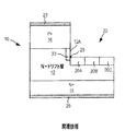
【解決手段】第1の伝導型を有するドリフト層と、前記ドリフト層上にあって、前記第1の伝導型とは反対の第2の伝導型を有し、前記ドリフト層とP−N接合を形成するバッファ層と、前記P−N接合の近傍の前記ドリフト層内にあって前記第2の伝導型を有する接合終端拡張領域とを含む電子デバイスを提供する。前記バッファ層は、前記接合終端拡張領域の埋め込み部分上を延びる階段部分を含む。関連する方法も開示される。
【選択図】図2A
Description
Claims (24)
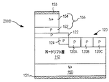
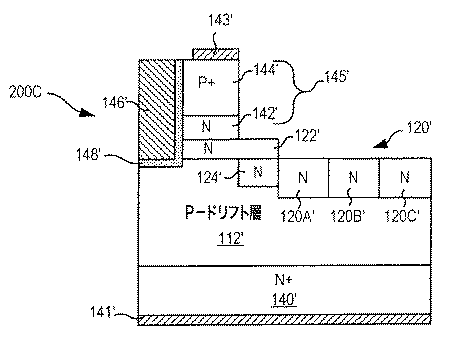
- 第1の伝導型を持ち第1の部分と第2の部分とを含むドリフト層と、
前記ドリフト層上にあって第2の伝導型を持ち、第3の部分と第4の部分とを有するバッファ層であって、前記バッファ層は、前記ドリフト層の前記第1の部分上にあって前記ドリフト層とP−N接合を形成する第1のメサを区画し、前記バッファ層は、前記ドリフト層の前記第2の部分上にはないことを特徴とするバッファ層と、
前記バッファ層上にあって前記ドリフト層とは反対側にあり、前記第2の伝導型をもつ第2の層であって、前記第2の層は、前記バッファ層の前記第3の部分上にあって、前記ドリフト層の前記第2の部分の近傍の前記バッファ層の前記第4の部分上にはない第2のメサを区画することを特徴とする第2の層と、
前記ドリフト層の前記第2の部分内にある接合終端領域であって、前記接合終端領域は、前記第2の伝導型を持つことを特徴とする接合終端領域と、
前記ドリフト層の前記第1の部分内にあって、前記第2の伝導型をもち、前記バッファ層と直接接触していて、少なくとも1部分は前記バッファ層の前記第4の部分の下にある埋め込み接合拡張部と
を備えた電子デバイス。 - 前記バッファ層は、約0.2から0.3μmの厚さを有することを特徴とする、請求項1に記載の電子デバイス。
- 前記バッファ層は、前記ドリフト層の正味のドーピング濃度より大きな正味のドーピング濃度を有することを特徴とする、請求項1に記載の電子デバイス。
- 前記バッファ層の前記正味のドーピング濃度は、前記第2の層の正味のドーピング濃度より少ないことを特徴とする、請求項3に記載の電子デバイス。
- 前記バッファ層の前記正味のドーピング濃度は、約lxl017cm-3であることを特徴とする、請求項1に記載の電子デバイス。
- 前記埋め込み接合拡張部は、約lxl016cm-3と約lxl018cm-3の間の正味のドーピング濃度を有し、前記ドリフト層の中へ前記バッファ層の下へ0.3μmの深さまで拡がっていることを特徴とする、請求項1に記載の電子デバイス。
- 前記第1のメサは、前記ドリフト層の表面上にあり、前記第1のメサは、前記ドリフト層の前記表面に対して前記第2のメサを通り過ぎて約10μmまたはそれ以上の幅で横に伸びていることを特徴とする、請求項1に記載の電子デバイス。
- 前記埋め込み接合拡張部は、イオン注入された領域を含むことを特徴とする、請求項1に記載の電子デバイス。
- 前記接合終端領域は、複数の接合終端拡張(JTE)地帯を含む接合終端拡張(JTE)領域を備えることを特徴とする、請求項1に記載の電子デバイス。
- 前記埋め込み接合拡張部は、前記JTE地帯の第1の地帯の横に隣接し、直接接触していることを特徴とする、請求項1に記載の電子デバイス。
- 前記埋め込み接合拡張部と前記第1のJTE地帯とは、同じドーピング濃度を有することを特徴とする、請求項10に記載の電子デバイス。
- 前記埋め込み接合拡張部の第1の側は、前記第1のメサの側壁と垂直方向に一直線に揃い、前記埋め込み接合拡張部の第2の側は、前記第2のメサの側壁と垂直方向に一直線に揃っていることを特徴とする、請求項1に記載の電子デバイス。
- 前記ドリフト層と前記バッファ層との前記P−N接合は、少なくとも約1kVの逆方向電圧を維持するように構成されていることを特徴とする、請求項1に記載の電子デバイス。
- 前記ドリフト層と前記バッファ層とは、炭化珪素の層を備えることを特徴とする、請求項1に記載の電子デバイス。
- 前記第2の伝導型は、前記第1の伝導型とは反対であることを特徴とする、請求項1に記載の電子デバイス。
- 第1の伝導型を有するドリフト層と、
前記ドリフト層上にあって第2の伝導型を有する第1の層であって、前記第1の層は、前記ドリフト層の表面の第1の部分を横切って伸び、前記ドリフト層とP−N接合を形成し、前記ドリフト層の前記表面の第2の部分を露出させるメサを含むことを特徴とし、前記第1の層は、主要部分と、前記主要部分から横方向に前記ドリフト層の前記表面を横切って伸び、前記第1の層の前記主要部分と比べて薄い厚さを持つ階段部分とを備えることを特徴とする第1の層と、
前記ドリフト層の表面で前記階段部分の下にあって、前記第2の伝導型を有する埋め込み接合拡張部と、
前記ドリフト層の前記表面にあって、前記埋め込み接合拡張部から延伸している接合終端部であって、前記接合終端部は、前記第2の伝導型を有し、前記埋め込み接合拡張部と直接接触していることを特徴とする接合終端部と
を備えた電力半導体デバイス。 - 前記第2の伝導型は、前記第1の伝導型とは反対であることを特徴とする、請求項16に記載の電力半導体デバイス。
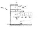
- 第1の伝導型を有するドリフト層と、
前記ドリフト層上にあって第2の伝導型を有し、前記ドリフト層とP−N接合を形成するバッファ層と、
前記P−N接合に隣接して前記ドリフト層内に前記第2の伝導型を有する接合終端拡張領域と
を備え、前記バッファ層は、前記接合終端拡張領域の埋め込み部分上に伸びる階段部分を備えることを特徴とする電子デバイス。 - 前記第2の伝導型は、前記第1の伝導型とは反対であることを特徴とする、請求項18に記載の電子デバイス。
- 電子デバイスを形成する方法であって、
第1の伝導型を有するドリフト層上に第2の伝導型を有する、準備段階のバッファ層を形成するステップと、
前記準備段階のバッファ層上にあって前記第2の伝導型を有する第1の層を形成するステップと、
前記準備段階のバッファ層の一部分を露出させる第1のメサを形成するために前記第1の層を選択的にエッチングするステップと、
前記ドリフト層の第1の部分を覆い、前記ドリフト層の第2の部分を露出させ、前記第1のメサから突出したメサ状階段を含む第2のメサを形成するために、前記準備段階のバッファ層の前記露出された一部分を選択的にエッチングするステップと、
前記ドリフト層内に接合終端領域を形成するために、前記第2のメサに隣接した前記ドリフト層内へ第2の伝導型のドーパントを選択的にイオン注入するステップと、
前記ドリフト層内に埋め込み接合拡張部を形成するために、前記メサ状階段の下の前記ドリフト層の1部分に前記メサ状階段を通して第2の伝導型のドーパントを選択的にイオン注入するステップと
を備えた方法。 - 前記第2の伝導型は、前記第1の伝導型とは反対であることを特徴とする、請求項20に記載の方法。
- 前記バッファ層は、約0.2から0.3μmの厚さを有し、前記埋め込み接合拡張部は、約lxl016cm-3から約4xl017cm-3の間の正味のドーピング濃度を有しすることを特徴とする、請求項20に記載の方法。
- 前記埋め込み接合拡張部の第1の側は、前記第1のメサの側壁と垂直方向に一直線に揃い、前記埋め込み接合拡張部の第2の側は、前記第2のメサの側壁と垂直方向に一直線に揃っていることを特徴とする、請求項20に記載の方法。
- 前記埋め込み接合拡張部は、前記ドリフト層の中へ前記バッファ層の下へ0.3μmの深さまで拡がっていることを特徴とする、請求項20に記載の方法。
Applications Claiming Priority (2)
| Application Number | Priority Date | Filing Date | Title |
|---|---|---|---|
| US12/189,551 | 2008-08-11 | ||
| US12/189,551 US8097919B2 (en) | 2008-08-11 | 2008-08-11 | Mesa termination structures for power semiconductor devices including mesa step buffers |
Publications (2)
| Publication Number | Publication Date |
|---|---|
| JP2010045363A true JP2010045363A (ja) | 2010-02-25 |
| JP5185228B2 JP5185228B2 (ja) | 2013-04-17 |
Family
ID=41280404
Family Applications (1)
| Application Number | Title | Priority Date | Filing Date |
|---|---|---|---|
| JP2009186765A Active JP5185228B2 (ja) | 2008-08-11 | 2009-08-11 | 電力半導体デバイスのためのメサ終端構造とメサ終端構造をもつ電力半導体デバイスを形成するための方法 |
Country Status (3)
| Country | Link |
|---|---|
| US (2) | US8097919B2 (ja) |
| EP (1) | EP2154723B1 (ja) |
| JP (1) | JP5185228B2 (ja) |
Cited By (16)
| Publication number | Priority date | Publication date | Assignee | Title |
|---|---|---|---|---|
| US20120018737A1 (en) * | 2010-07-21 | 2012-01-26 | Cree, Inc. | Electronic device structure including a buffer layer on a base layer |
| JP2012256664A (ja) * | 2011-06-08 | 2012-12-27 | Advanced Power Device Research Association | メサ型ダイオードおよびメサ型ダイオードの製造方法 |
| US8525189B2 (en) | 2010-11-26 | 2013-09-03 | Mitsubishi Electric Corporation | Silicon carbide semiconductor device |
| JP2013211460A (ja) * | 2012-03-30 | 2013-10-10 | National Institute Of Advanced Industrial & Technology | 高耐圧半導体装置 |
| US8748276B2 (en) | 2011-07-14 | 2014-06-10 | Sumitomo Electric Industries, Ltd. | Method for manufacturing semiconductor device |
| US8841741B2 (en) | 2011-03-10 | 2014-09-23 | Kabushiki Kaisha Toshiba | High breakdown voltage semiconductor rectifier |
| JP2015510272A (ja) * | 2012-02-06 | 2015-04-02 | クリー インコーポレイテッドCree Inc. | 負ベベルにより終端した、高い阻止電圧を有するSiC素子 |
| JP2015204411A (ja) * | 2014-04-15 | 2015-11-16 | 住友電気工業株式会社 | 炭化珪素半導体装置 |
| JP2016092331A (ja) * | 2014-11-10 | 2016-05-23 | 富士電機株式会社 | 半導体装置 |
| JP2016167632A (ja) * | 2016-05-17 | 2016-09-15 | 住友電気工業株式会社 | 炭化珪素半導体装置 |
| JP2016189480A (ja) * | 2011-05-16 | 2016-11-04 | クリー インコーポレイテッドCree Inc. | 負べベルにより終端された高阻止電圧を有するSiCデバイス |
| JP2018107441A (ja) * | 2016-12-17 | 2018-07-05 | 3−5 パワー エレクトロニクス ゲゼルシャフト ミット ベシュレンクテル ハフツング3−5 Power Electronics GmbH | p+基板、p−層、n−層および第3の層から成る層スタックの製造方法 |
| JP2018164083A (ja) * | 2017-03-24 | 2018-10-18 | 3−5 パワー エレクトロニクス ゲゼルシャフト ミット ベシュレンクテル ハフツング3−5 Power Electronics GmbH | Iii−v族半導体ダイオード |
| US10134920B2 (en) | 2015-10-30 | 2018-11-20 | Mitsubishi Electric Corporation | Silicon carbide semiconductor device |
| JP2019067982A (ja) * | 2017-10-03 | 2019-04-25 | 富士電機株式会社 | 炭化珪素半導体装置 |
| JP2021019156A (ja) * | 2019-07-23 | 2021-02-15 | 富士電機株式会社 | 炭化珪素半導体装置 |
Families Citing this family (49)
| Publication number | Priority date | Publication date | Assignee | Title |
|---|---|---|---|---|
| US8432012B2 (en) | 2006-08-01 | 2013-04-30 | Cree, Inc. | Semiconductor devices including schottky diodes having overlapping doped regions and methods of fabricating same |
| US7728402B2 (en) | 2006-08-01 | 2010-06-01 | Cree, Inc. | Semiconductor devices including schottky diodes with controlled breakdown |
| KR101529331B1 (ko) | 2006-08-17 | 2015-06-16 | 크리 인코포레이티드 | 고전력 절연 게이트 바이폴라 트랜지스터 |
| US8835987B2 (en) | 2007-02-27 | 2014-09-16 | Cree, Inc. | Insulated gate bipolar transistors including current suppressing layers |
| US9640609B2 (en) * | 2008-02-26 | 2017-05-02 | Cree, Inc. | Double guard ring edge termination for silicon carbide devices |
| US8497552B2 (en) * | 2008-12-01 | 2013-07-30 | Cree, Inc. | Semiconductor devices with current shifting regions and related methods |
| US8536582B2 (en) * | 2008-12-01 | 2013-09-17 | Cree, Inc. | Stable power devices on low-angle off-cut silicon carbide crystals |
| CN101494239B (zh) * | 2009-02-27 | 2010-12-01 | 电子科技大学 | 一种高速igbt |
| US8637386B2 (en) * | 2009-05-12 | 2014-01-28 | Cree, Inc. | Diffused junction termination structures for silicon carbide devices and methods of fabricating silicon carbide devices incorporating same |
| US8193848B2 (en) | 2009-06-02 | 2012-06-05 | Cree, Inc. | Power switching devices having controllable surge current capabilities |
| US8629509B2 (en) * | 2009-06-02 | 2014-01-14 | Cree, Inc. | High voltage insulated gate bipolar transistors with minority carrier diverter |
| US8541787B2 (en) * | 2009-07-15 | 2013-09-24 | Cree, Inc. | High breakdown voltage wide band-gap MOS-gated bipolar junction transistors with avalanche capability |
| US8354690B2 (en) | 2009-08-31 | 2013-01-15 | Cree, Inc. | Solid-state pinch off thyristor circuits |
| US9117739B2 (en) | 2010-03-08 | 2015-08-25 | Cree, Inc. | Semiconductor devices with heterojunction barrier regions and methods of fabricating same |
| US8415671B2 (en) | 2010-04-16 | 2013-04-09 | Cree, Inc. | Wide band-gap MOSFETs having a heterojunction under gate trenches thereof and related methods of forming such devices |
| US8278711B2 (en) * | 2010-11-23 | 2012-10-02 | General Electric Company | Semiconductor device and method of making the same |
| US8803277B2 (en) | 2011-02-10 | 2014-08-12 | Cree, Inc. | Junction termination structures including guard ring extensions and methods of fabricating electronic devices incorporating same |
| US9673283B2 (en) | 2011-05-06 | 2017-06-06 | Cree, Inc. | Power module for supporting high current densities |
| US9029945B2 (en) | 2011-05-06 | 2015-05-12 | Cree, Inc. | Field effect transistor devices with low source resistance |
| US9142662B2 (en) | 2011-05-06 | 2015-09-22 | Cree, Inc. | Field effect transistor devices with low source resistance |
| US8723218B2 (en) * | 2011-09-08 | 2014-05-13 | The United States Of America, As Represented By The Secretary Of The Navy | Silicon carbide rectifier |
| US9640617B2 (en) | 2011-09-11 | 2017-05-02 | Cree, Inc. | High performance power module |
| US8680587B2 (en) | 2011-09-11 | 2014-03-25 | Cree, Inc. | Schottky diode |
| US8618582B2 (en) | 2011-09-11 | 2013-12-31 | Cree, Inc. | Edge termination structure employing recesses for edge termination elements |
| US9373617B2 (en) | 2011-09-11 | 2016-06-21 | Cree, Inc. | High current, low switching loss SiC power module |
| US8664665B2 (en) | 2011-09-11 | 2014-03-04 | Cree, Inc. | Schottky diode employing recesses for elements of junction barrier array |
| US8822311B2 (en) * | 2011-12-22 | 2014-09-02 | Avogy, Inc. | Method of fabricating a GaN P-i-N diode using implantation |
| US8927999B2 (en) | 2011-11-21 | 2015-01-06 | Avogy, Inc. | Edge termination by ion implantation in GaN |
| US8716716B2 (en) * | 2011-12-22 | 2014-05-06 | Avogy, Inc. | Method and system for junction termination in GaN materials using conductivity modulation |
| WO2013107508A1 (en) * | 2012-01-18 | 2013-07-25 | Fairchild Semiconductor Corporation | Bipolar junction transistor with spacer layer and method of manufacturing the same |
| CN104303314B (zh) * | 2012-05-17 | 2017-05-24 | 通用电气公司 | 具有结终端扩展的半导体器件 |
| US20140001514A1 (en) | 2012-07-02 | 2014-01-02 | Infineon Technologies Ag | Semiconductor Device and Method for Producing a Doped Semiconductor Layer |
| JP2014241367A (ja) * | 2013-06-12 | 2014-12-25 | 三菱電機株式会社 | 半導体素子、半導体素子の製造方法 |
| US9245944B2 (en) * | 2013-07-02 | 2016-01-26 | Infineon Technologies Ag | Silicon carbide device and a method for manufacturing a silicon carbide device |
| US9064738B2 (en) * | 2013-07-19 | 2015-06-23 | Cree, Inc. | Methods of forming junction termination extension edge terminations for high power semiconductor devices and related semiconductor devices |
| US9768259B2 (en) | 2013-07-26 | 2017-09-19 | Cree, Inc. | Controlled ion implantation into silicon carbide using channeling and devices fabricated using controlled ion implantation into silicon carbide using channeling |
| US9425265B2 (en) | 2013-08-16 | 2016-08-23 | Cree, Inc. | Edge termination technique for high voltage power devices having a negative feature for an improved edge termination structure |
| JP6178181B2 (ja) * | 2013-09-12 | 2017-08-09 | 株式会社東芝 | 半導体装置及びその製造方法 |
| TWI497665B (zh) | 2013-10-16 | 2015-08-21 | A silicon carbide power element with a terminal structure | |
| WO2016014224A1 (en) * | 2014-07-25 | 2016-01-28 | United Silicon Carbide, Inc. | Self-aligned shielded-gate trench mos-controlled silicon carbide switch with reduced miller capacitance and method of manufacturing the same |
| JP6871562B2 (ja) * | 2016-11-16 | 2021-05-12 | 富士電機株式会社 | 炭化珪素半導体素子およびその製造方法 |
| DE102017117442B3 (de) | 2017-08-01 | 2019-01-24 | Infineon Technologies Ag | Transistorbauelement mit Grabenrandabschluss |
| JP2019054170A (ja) * | 2017-09-15 | 2019-04-04 | 株式会社東芝 | 半導体装置 |
| DE102018113573B4 (de) * | 2018-06-07 | 2022-11-03 | Semikron Elektronik Gmbh & Co. Kg Patentabteilung | Diode mit einem Halbleiterkörper |
| CN109950300B (zh) * | 2019-03-04 | 2021-12-10 | 中国工程物理研究院电子工程研究所 | 基于漂移区阶梯刻蚀的双向耐压功率器件逆向终端结构 |
| DE102019216138A1 (de) * | 2019-10-21 | 2021-04-22 | Robert Bosch Gmbh | Vertikaler feldeffekttransistor und verfahren zum ausbilden desselben |
| CN113219819B (zh) * | 2021-02-09 | 2022-10-25 | 兰州空间技术物理研究所 | 一种基于Matlab/Simulink的静电悬浮加速度计落塔实验仿真系统 |
| US20240128323A1 (en) * | 2021-02-22 | 2024-04-18 | The Research Foundation for the State Universtiy of New York | Metal oxide semiconductor field effect transistors (mosfet) including deep p-wells and methods of forming same |
| KR102884352B1 (ko) * | 2024-01-10 | 2025-11-13 | 한국전자통신연구원 | 질화물 반도체 소자 및 이의 제조방법 |
Citations (3)
| Publication number | Priority date | Publication date | Assignee | Title |
|---|---|---|---|---|
| JPS556887A (en) * | 1978-06-06 | 1980-01-18 | Gen Electric | Semiconductor having high breakdown voltage |
| US6083814A (en) * | 1998-08-31 | 2000-07-04 | Abb Research Ltd. | Method for producing a pn-junction for a semiconductor device of SiC |
| JP2002516027A (ja) * | 1995-08-30 | 2002-05-28 | アセア ブラウン ボベリ アクチボラグ | 電圧吸収端部を有するpn接合を含むSiC半導体デバイス |
Family Cites Families (35)
| Publication number | Priority date | Publication date | Assignee | Title |
|---|---|---|---|---|
| EP0176778B1 (de) | 1984-09-28 | 1991-01-16 | Siemens Aktiengesellschaft | Verfahren zum Herstellen eines pn-Übergangs mit hoher Durchbruchsspannung |
| US4742377A (en) | 1985-02-21 | 1988-05-03 | General Instrument Corporation | Schottky barrier device with doped composite guard ring |
| DE59010606D1 (de) | 1989-03-29 | 1997-01-30 | Siemens Ag | Verfahren zur Herstellung eines planaren pn-Übergangs hoher Spannungsfestigkeit |
| US4927772A (en) * | 1989-05-30 | 1990-05-22 | General Electric Company | Method of making high breakdown voltage semiconductor device |
| GB8913198D0 (en) | 1989-06-08 | 1989-07-26 | British Telecomm | Guard ring structure |
| JPH03225870A (ja) | 1990-01-31 | 1991-10-04 | Toshiba Corp | ヘテロ接合バイポーラトランジスタの製造方法 |
| CN1040814C (zh) * | 1994-07-20 | 1998-11-18 | 电子科技大学 | 一种用于半导体器件的表面耐压区 |
| TW286435B (ja) | 1994-07-27 | 1996-09-21 | Siemens Ag | |
| SE9602745D0 (sv) | 1996-07-11 | 1996-07-11 | Abb Research Ltd | A method for producing a channel region layer in a SiC-layer for a voltage controlled semiconductor device |
| US6002159A (en) | 1996-07-16 | 1999-12-14 | Abb Research Ltd. | SiC semiconductor device comprising a pn junction with a voltage absorbing edge |
| JP3225870B2 (ja) | 1996-12-05 | 2001-11-05 | トヨタ車体株式会社 | ルーフスポイラの取付構造 |
| SE9700156D0 (sv) | 1997-01-21 | 1997-01-21 | Abb Research Ltd | Junction termination for Si C Schottky diode |
| WO2000042662A1 (de) * | 1999-01-12 | 2000-07-20 | eupec Europäische Gesellschaft für Leistungshalbleiter mbH & Co. KG | Leistungshalbleiterbauelement mit mesa-randabschluss |
| JP2001035857A (ja) | 1999-07-21 | 2001-02-09 | Nec Corp | 化合物ヘテロバイポーラトランジスタおよびその製造方法 |
| US7026650B2 (en) * | 2003-01-15 | 2006-04-11 | Cree, Inc. | Multiple floating guard ring edge termination for silicon carbide devices |
| CN100483733C (zh) | 2003-01-15 | 2009-04-29 | 克里公司 | 碳化硅器件的边缘环形端接 |
| US7109521B2 (en) | 2004-03-18 | 2006-09-19 | Cree, Inc. | Silicon carbide semiconductor structures including multiple epitaxial layers having sidewalls |
| US7144797B2 (en) | 2004-09-24 | 2006-12-05 | Rensselaer Polytechnic Institute | Semiconductor device having multiple-zone junction termination extension, and method for fabricating the same |
| JP3914226B2 (ja) * | 2004-09-29 | 2007-05-16 | 株式会社東芝 | 高耐圧半導体装置 |
| US7498651B2 (en) | 2004-11-24 | 2009-03-03 | Microsemi Corporation | Junction termination structures for wide-bandgap power devices |
| US7304363B1 (en) * | 2004-11-26 | 2007-12-04 | United States Of America As Represented By The Secretary Of The Army | Interacting current spreader and junction extender to increase the voltage blocked in the off state of a high power semiconductor device |
| DE102005023668B3 (de) | 2005-05-23 | 2006-11-09 | Infineon Technologies Ag | Halbleiterbauelement mit einer Randstruktur mit Spannungsdurchbruch im linearen Bereich |
| JP4755854B2 (ja) | 2005-06-02 | 2011-08-24 | 富士通株式会社 | 半導体受光装置及びその製造方法 |
| JP4777699B2 (ja) | 2005-06-13 | 2011-09-21 | 本田技研工業株式会社 | バイポーラ型半導体装置およびその製造方法 |
| US8084815B2 (en) | 2005-06-29 | 2011-12-27 | Fairchild Korea Semiconductor Ltd. | Superjunction semiconductor device |
| US7304334B2 (en) | 2005-09-16 | 2007-12-04 | Cree, Inc. | Silicon carbide bipolar junction transistors having epitaxial base regions and multilayer emitters and methods of fabricating the same |
| JP2007103784A (ja) * | 2005-10-06 | 2007-04-19 | Matsushita Electric Ind Co Ltd | ヘテロ接合バイポーラトランジスタ |
| US7345310B2 (en) | 2005-12-22 | 2008-03-18 | Cree, Inc. | Silicon carbide bipolar junction transistors having a silicon carbide passivation layer on the base region thereof |
| JP2007287782A (ja) * | 2006-04-13 | 2007-11-01 | Hitachi Ltd | メサ型バイポーラトランジスタ |
| US7372087B2 (en) * | 2006-06-01 | 2008-05-13 | Northrop Grumman Corporation | Semiconductor structure for use in a static induction transistor having improved gate-to-drain breakdown voltage |
| US7883949B2 (en) | 2006-06-29 | 2011-02-08 | Cree, Inc | Methods of forming silicon carbide switching devices including P-type channels |
| KR101529331B1 (ko) | 2006-08-17 | 2015-06-16 | 크리 인코포레이티드 | 고전력 절연 게이트 바이폴라 트랜지스터 |
| JP5372002B2 (ja) * | 2007-11-09 | 2013-12-18 | クリー インコーポレイテッド | メサ構造とメサ段差を含むバッファ層とを備えた電力半導体デバイス |
| US9640609B2 (en) | 2008-02-26 | 2017-05-02 | Cree, Inc. | Double guard ring edge termination for silicon carbide devices |
| US8637386B2 (en) | 2009-05-12 | 2014-01-28 | Cree, Inc. | Diffused junction termination structures for silicon carbide devices and methods of fabricating silicon carbide devices incorporating same |
-
2008
- 2008-08-11 US US12/189,551 patent/US8097919B2/en active Active
-
2009
- 2009-06-22 EP EP09163424.6A patent/EP2154723B1/en active Active
- 2009-08-11 JP JP2009186765A patent/JP5185228B2/ja active Active
-
2011
- 2011-12-28 US US13/338,620 patent/US8460977B2/en active Active
Patent Citations (3)
| Publication number | Priority date | Publication date | Assignee | Title |
|---|---|---|---|---|
| JPS556887A (en) * | 1978-06-06 | 1980-01-18 | Gen Electric | Semiconductor having high breakdown voltage |
| JP2002516027A (ja) * | 1995-08-30 | 2002-05-28 | アセア ブラウン ボベリ アクチボラグ | 電圧吸収端部を有するpn接合を含むSiC半導体デバイス |
| US6083814A (en) * | 1998-08-31 | 2000-07-04 | Abb Research Ltd. | Method for producing a pn-junction for a semiconductor device of SiC |
Cited By (24)
| Publication number | Priority date | Publication date | Assignee | Title |
|---|---|---|---|---|
| US8552435B2 (en) * | 2010-07-21 | 2013-10-08 | Cree, Inc. | Electronic device structure including a buffer layer on a base layer |
| US20120018737A1 (en) * | 2010-07-21 | 2012-01-26 | Cree, Inc. | Electronic device structure including a buffer layer on a base layer |
| JP2013543648A (ja) * | 2010-07-21 | 2013-12-05 | クリー インコーポレイテッド | ベース層上に緩衝層を備える電子デバイス構造 |
| US8932944B2 (en) | 2010-11-26 | 2015-01-13 | Mitsubishi Electric Corporation | Silicon carbide semiconductor device manufacturing method |
| US8525189B2 (en) | 2010-11-26 | 2013-09-03 | Mitsubishi Electric Corporation | Silicon carbide semiconductor device |
| US8841741B2 (en) | 2011-03-10 | 2014-09-23 | Kabushiki Kaisha Toshiba | High breakdown voltage semiconductor rectifier |
| JP2016189480A (ja) * | 2011-05-16 | 2016-11-04 | クリー インコーポレイテッドCree Inc. | 負べベルにより終端された高阻止電圧を有するSiCデバイス |
| JP2012256664A (ja) * | 2011-06-08 | 2012-12-27 | Advanced Power Device Research Association | メサ型ダイオードおよびメサ型ダイオードの製造方法 |
| US8748276B2 (en) | 2011-07-14 | 2014-06-10 | Sumitomo Electric Industries, Ltd. | Method for manufacturing semiconductor device |
| JP2015510272A (ja) * | 2012-02-06 | 2015-04-02 | クリー インコーポレイテッドCree Inc. | 負ベベルにより終端した、高い阻止電圧を有するSiC素子 |
| CN104321875A (zh) * | 2012-03-30 | 2015-01-28 | 富士电机株式会社 | 高耐压半导体装置 |
| JP2013211460A (ja) * | 2012-03-30 | 2013-10-10 | National Institute Of Advanced Industrial & Technology | 高耐圧半導体装置 |
| CN104321875B (zh) * | 2012-03-30 | 2017-05-24 | 富士电机株式会社 | 高耐压半导体装置 |
| US9450051B2 (en) | 2012-03-30 | 2016-09-20 | Fuji Electric Co., Ltd. | High voltage semiconductor apparatus |
| JP2015204411A (ja) * | 2014-04-15 | 2015-11-16 | 住友電気工業株式会社 | 炭化珪素半導体装置 |
| JP2016092331A (ja) * | 2014-11-10 | 2016-05-23 | 富士電機株式会社 | 半導体装置 |
| US10134920B2 (en) | 2015-10-30 | 2018-11-20 | Mitsubishi Electric Corporation | Silicon carbide semiconductor device |
| JP2016167632A (ja) * | 2016-05-17 | 2016-09-15 | 住友電気工業株式会社 | 炭化珪素半導体装置 |
| JP2018107441A (ja) * | 2016-12-17 | 2018-07-05 | 3−5 パワー エレクトロニクス ゲゼルシャフト ミット ベシュレンクテル ハフツング3−5 Power Electronics GmbH | p+基板、p−層、n−層および第3の層から成る層スタックの製造方法 |
| JP2018164083A (ja) * | 2017-03-24 | 2018-10-18 | 3−5 パワー エレクトロニクス ゲゼルシャフト ミット ベシュレンクテル ハフツング3−5 Power Electronics GmbH | Iii−v族半導体ダイオード |
| US10734532B2 (en) | 2017-03-24 | 2020-08-04 | 3-5 Power Electronics GmbH | III-V semiconductor diode |
| JP2019067982A (ja) * | 2017-10-03 | 2019-04-25 | 富士電機株式会社 | 炭化珪素半導体装置 |
| JP2021019156A (ja) * | 2019-07-23 | 2021-02-15 | 富士電機株式会社 | 炭化珪素半導体装置 |
| JP7388027B2 (ja) | 2019-07-23 | 2023-11-29 | 富士電機株式会社 | 炭化珪素半導体装置 |
Also Published As
| Publication number | Publication date |
|---|---|
| JP5185228B2 (ja) | 2013-04-17 |
| EP2154723B1 (en) | 2020-03-04 |
| US20100032685A1 (en) | 2010-02-11 |
| US20120122305A1 (en) | 2012-05-17 |
| EP2154723A3 (en) | 2010-05-05 |
| EP2154723A2 (en) | 2010-02-17 |
| US8097919B2 (en) | 2012-01-17 |
| US8460977B2 (en) | 2013-06-11 |
Similar Documents
| Publication | Publication Date | Title |
|---|---|---|
| JP5185228B2 (ja) | 電力半導体デバイスのためのメサ終端構造とメサ終端構造をもつ電力半導体デバイスを形成するための方法 | |
| JP7182594B2 (ja) | ゲート・トレンチと、埋め込まれた終端構造とを有するパワー半導体デバイス、及び、関連方法 | |
| JP5372002B2 (ja) | メサ構造とメサ段差を含むバッファ層とを備えた電力半導体デバイス | |
| US9318623B2 (en) | Recessed termination structures and methods of fabricating electronic devices including recessed termination structures | |
| JP4564510B2 (ja) | 電力用半導体素子 | |
| JP5101985B2 (ja) | ジャンクションバリアショットキーダイオード | |
| US8643091B2 (en) | Semiconductor device | |
| CN103443907B (zh) | 包括具有重叠掺杂区的肖特基二极管的半导体器件及其制造方法 | |
| CN103460392B (zh) | 半导体装置及其制造方法 | |
| KR101802419B1 (ko) | 트렌치형 필러 옥사이드를 이용한 탄화규소 슈퍼정션 모스펫 및 그 제조방법 | |
| KR20100128303A (ko) | 실리콘 카바이드 디바이스를 위한 이중 가드 링 에지 종단 및 이를 포함하는 실리콘 카바이드 디바이스를 제조하는 방법 | |
| CN107210318A (zh) | 高压半导体设备 | |
| CN105917470A (zh) | 碳化硅沟槽晶体管以及用于制造碳化硅沟槽晶体管的方法 | |
| WO2017204964A1 (en) | Semiconductor device and method of making thereof |
Legal Events
| Date | Code | Title | Description |
|---|---|---|---|
| RD02 | Notification of acceptance of power of attorney |
Free format text: JAPANESE INTERMEDIATE CODE: A7422 Effective date: 20101207 |
|
| RD04 | Notification of resignation of power of attorney |
Free format text: JAPANESE INTERMEDIATE CODE: A7424 Effective date: 20110302 |
|
| A977 | Report on retrieval |
Free format text: JAPANESE INTERMEDIATE CODE: A971007 Effective date: 20120501 |
|
| A131 | Notification of reasons for refusal |
Free format text: JAPANESE INTERMEDIATE CODE: A131 Effective date: 20120508 |
|
| A601 | Written request for extension of time |
Free format text: JAPANESE INTERMEDIATE CODE: A601 Effective date: 20120808 |
|
| A602 | Written permission of extension of time |
Free format text: JAPANESE INTERMEDIATE CODE: A602 Effective date: 20120813 |
|
| A601 | Written request for extension of time |
Free format text: JAPANESE INTERMEDIATE CODE: A601 Effective date: 20120910 |
|
| A602 | Written permission of extension of time |
Free format text: JAPANESE INTERMEDIATE CODE: A602 Effective date: 20120913 |
|
| A601 | Written request for extension of time |
Free format text: JAPANESE INTERMEDIATE CODE: A601 Effective date: 20121009 |
|
| A602 | Written permission of extension of time |
Free format text: JAPANESE INTERMEDIATE CODE: A602 Effective date: 20121012 |
|
| A521 | Request for written amendment filed |
Free format text: JAPANESE INTERMEDIATE CODE: A523 Effective date: 20121016 |
|
| TRDD | Decision of grant or rejection written | ||
| A01 | Written decision to grant a patent or to grant a registration (utility model) |
Free format text: JAPANESE INTERMEDIATE CODE: A01 Effective date: 20130104 |
|
| A61 | First payment of annual fees (during grant procedure) |
Free format text: JAPANESE INTERMEDIATE CODE: A61 Effective date: 20130117 |
|
| R150 | Certificate of patent or registration of utility model |
Ref document number: 5185228 Country of ref document: JP Free format text: JAPANESE INTERMEDIATE CODE: R150 Free format text: JAPANESE INTERMEDIATE CODE: R150 |
|
| FPAY | Renewal fee payment (event date is renewal date of database) |
Free format text: PAYMENT UNTIL: 20160125 Year of fee payment: 3 |
|
| R250 | Receipt of annual fees |
Free format text: JAPANESE INTERMEDIATE CODE: R250 |
|
| R250 | Receipt of annual fees |
Free format text: JAPANESE INTERMEDIATE CODE: R250 |
|
| R250 | Receipt of annual fees |
Free format text: JAPANESE INTERMEDIATE CODE: R250 |
|
| R250 | Receipt of annual fees |
Free format text: JAPANESE INTERMEDIATE CODE: R250 |
|
| R250 | Receipt of annual fees |
Free format text: JAPANESE INTERMEDIATE CODE: R250 |
|
| R250 | Receipt of annual fees |
Free format text: JAPANESE INTERMEDIATE CODE: R250 |
|
| R250 | Receipt of annual fees |
Free format text: JAPANESE INTERMEDIATE CODE: R250 |
|
| R250 | Receipt of annual fees |
Free format text: JAPANESE INTERMEDIATE CODE: R250 |
|
| R250 | Receipt of annual fees |
Free format text: JAPANESE INTERMEDIATE CODE: R250 |
|
| R250 | Receipt of annual fees |
Free format text: JAPANESE INTERMEDIATE CODE: R250 |
|
| R250 | Receipt of annual fees |
Free format text: JAPANESE INTERMEDIATE CODE: R250 |