JP2010008758A - 液晶表示パネル - Google Patents
液晶表示パネル Download PDFInfo
- Publication number
- JP2010008758A JP2010008758A JP2008168498A JP2008168498A JP2010008758A JP 2010008758 A JP2010008758 A JP 2010008758A JP 2008168498 A JP2008168498 A JP 2008168498A JP 2008168498 A JP2008168498 A JP 2008168498A JP 2010008758 A JP2010008758 A JP 2010008758A
- Authority
- JP
- Japan
- Prior art keywords
- liquid crystal
- display panel
- crystal display
- common electrode
- electrode
- Prior art date
- Legal status (The legal status is an assumption and is not a legal conclusion. Google has not performed a legal analysis and makes no representation as to the accuracy of the status listed.)
- Granted
Links
Images


Classifications
-
- G—PHYSICS
- G02—OPTICS
- G02F—OPTICAL DEVICES OR ARRANGEMENTS FOR THE CONTROL OF LIGHT BY MODIFICATION OF THE OPTICAL PROPERTIES OF THE MEDIA OF THE ELEMENTS INVOLVED THEREIN; NON-LINEAR OPTICS; FREQUENCY-CHANGING OF LIGHT; OPTICAL LOGIC ELEMENTS; OPTICAL ANALOGUE/DIGITAL CONVERTERS
- G02F1/00—Devices or arrangements for the control of the intensity, colour, phase, polarisation or direction of light arriving from an independent light source, e.g. switching, gating or modulating; Non-linear optics
- G02F1/01—Devices or arrangements for the control of the intensity, colour, phase, polarisation or direction of light arriving from an independent light source, e.g. switching, gating or modulating; Non-linear optics for the control of the intensity, phase, polarisation or colour
- G02F1/13—Devices or arrangements for the control of the intensity, colour, phase, polarisation or direction of light arriving from an independent light source, e.g. switching, gating or modulating; Non-linear optics for the control of the intensity, phase, polarisation or colour based on liquid crystals, e.g. single liquid crystal display cells
- G02F1/133—Constructional arrangements; Operation of liquid crystal cells; Circuit arrangements
- G02F1/1333—Constructional arrangements; Manufacturing methods
- G02F1/1345—Conductors connecting electrodes to cell terminals
-
- G—PHYSICS
- G02—OPTICS
- G02F—OPTICAL DEVICES OR ARRANGEMENTS FOR THE CONTROL OF LIGHT BY MODIFICATION OF THE OPTICAL PROPERTIES OF THE MEDIA OF THE ELEMENTS INVOLVED THEREIN; NON-LINEAR OPTICS; FREQUENCY-CHANGING OF LIGHT; OPTICAL LOGIC ELEMENTS; OPTICAL ANALOGUE/DIGITAL CONVERTERS
- G02F1/00—Devices or arrangements for the control of the intensity, colour, phase, polarisation or direction of light arriving from an independent light source, e.g. switching, gating or modulating; Non-linear optics
- G02F1/01—Devices or arrangements for the control of the intensity, colour, phase, polarisation or direction of light arriving from an independent light source, e.g. switching, gating or modulating; Non-linear optics for the control of the intensity, phase, polarisation or colour
- G02F1/13—Devices or arrangements for the control of the intensity, colour, phase, polarisation or direction of light arriving from an independent light source, e.g. switching, gating or modulating; Non-linear optics for the control of the intensity, phase, polarisation or colour based on liquid crystals, e.g. single liquid crystal display cells
- G02F1/133—Constructional arrangements; Operation of liquid crystal cells; Circuit arrangements
- G02F1/1333—Constructional arrangements; Manufacturing methods
- G02F1/1343—Electrodes
- G02F1/13439—Electrodes characterised by their electrical, optical, physical properties; materials therefor; method of making
-
- G—PHYSICS
- G02—OPTICS
- G02F—OPTICAL DEVICES OR ARRANGEMENTS FOR THE CONTROL OF LIGHT BY MODIFICATION OF THE OPTICAL PROPERTIES OF THE MEDIA OF THE ELEMENTS INVOLVED THEREIN; NON-LINEAR OPTICS; FREQUENCY-CHANGING OF LIGHT; OPTICAL LOGIC ELEMENTS; OPTICAL ANALOGUE/DIGITAL CONVERTERS
- G02F1/00—Devices or arrangements for the control of the intensity, colour, phase, polarisation or direction of light arriving from an independent light source, e.g. switching, gating or modulating; Non-linear optics
- G02F1/01—Devices or arrangements for the control of the intensity, colour, phase, polarisation or direction of light arriving from an independent light source, e.g. switching, gating or modulating; Non-linear optics for the control of the intensity, phase, polarisation or colour
- G02F1/13—Devices or arrangements for the control of the intensity, colour, phase, polarisation or direction of light arriving from an independent light source, e.g. switching, gating or modulating; Non-linear optics for the control of the intensity, phase, polarisation or colour based on liquid crystals, e.g. single liquid crystal display cells
- G02F1/133—Constructional arrangements; Operation of liquid crystal cells; Circuit arrangements
- G02F1/1333—Constructional arrangements; Manufacturing methods
- G02F1/1343—Electrodes
- G02F1/134309—Electrodes characterised by their geometrical arrangement
- G02F1/134372—Electrodes characterised by their geometrical arrangement for fringe field switching [FFS] where the common electrode is not patterned
Landscapes
- Physics & Mathematics (AREA)
- Nonlinear Science (AREA)
- Mathematical Physics (AREA)
- Chemical & Material Sciences (AREA)
- Crystallography & Structural Chemistry (AREA)
- General Physics & Mathematics (AREA)
- Optics & Photonics (AREA)
- Liquid Crystal (AREA)
Abstract
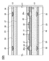
【解決手段】本発明の液晶表示パネル10Aは、層間膜24の表面に複数の走査線19及び信号線22で区画された画素領域毎に形成された透明導電性材料からなる画素電極25と、前記表示領域の画素電極25上及び層間膜24上に形成された電極間絶縁膜27と、前記電極間絶縁膜27上の全面に形成され、前記画素領域毎に複数のスリット31が形成されていると共に共通配線と電気的に接続された透明導電性材料からなる共通電極28とを備え、前記共通電極28の表面又は前記共通電極28と前記電極間絶縁膜27との間には、平面視で前記走査線19及び信号線22と重畳する位置に前記共通電極28を構成する透明導電性材料よりも導電性が良好な導電性層29aが形成されていることを特徴とする。
【選択図】図2
Description
第1実施形態に係る液晶表示パネル10Aを図1〜図4を用いて説明する。第1実施形態に係る液晶表示パネル10Aは、液晶層11をアレイ基板12及びカラーフィルタ基板13との間に挟持している。液晶層11の厚みは図示しない柱状スペーサによって均一に維持される。アレイ基板12の背面及びカラーフィルタ基板13の前面にはそれぞれ偏光板(いずれも図示省略)が貼付されており、また、アレイ基板12の背面側には光を照射するバックライト(図示省略)が配設されている。
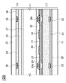
第1実施形態では導電性層29aを共通電極28の表面に形成した例を示したが、この導電性層29aは共通電極28と電極間絶縁膜27との間に形成することもできる。このような構成の第2実施形態の液晶表示パネル10Bを図5〜図7を用いて説明する。ただし、図5〜図7においては、図1〜図3に示した構成と同一の構成部分には同一の参照符号を付与してその詳細な説明は省略する。また、第2実施形態の液晶表示パネル10Bにおける共通電極28及び導電性層29bと共通配線40との間の電気的接続形態は、図4に示した第1の実施形態の液晶表示パネル10Aの場合と同様であるので、図示省略する。
Claims (6)
- 液晶層を挟持して対向配置された一対の基板を有し、前記一対の基板のうちの一方には、
表示領域にマトリクス状に配置された複数の走査線及び信号線と、
前記表示領域の周縁部に沿って形成された共通配線と、
少なくとも表示領域の全体に亘って形成された層間膜と、
前記層間膜の表面に前記複数の走査線及び信号線で区画された画素領域毎に形成された透明導電性材料からなる画素電極と、
前記表示領域の画素電極上及び層間膜上に形成された電極間絶縁膜と、
前記電極間絶縁膜上の全面に形成され、前記画素領域毎に複数のスリットが形成されていると共に前記共通配線と電気的に接続された透明導電性材料からなる共通電極と、
を備えた液晶表示パネルであって、
前記共通電極の表面又は前記共通電極と前記電極間絶縁膜との間には、平面視で前記走査線及び信号線と重畳する位置に前記共通電極を構成する透明導電性材料よりも導電性が良好な導電性層が形成されていることを特徴とする液晶表示パネル。 - 前記導電性層は遮光性であることを特徴とする請求項1に記載の液晶表示パネル。
- 前記導電性層は金属材料からなることを特徴とする請求項2に記載の液晶表示パネル。
- 前記導電性層の幅は前記走査線及び信号線の幅と同じか或いは細いことを特徴とする請求項2に記載の液晶表示パネル。
- 前記導電性層の幅は前記走査線及び信号線の幅よりも太いことを特徴とする請求項2に記載の液晶表示パネル。
- 前記導電性層は、前記表示領域の周辺部まで延在され、前記共通配線と直接電気的に接続されていることを特徴とする請求項1〜5のいずれかに記載の液晶表示パネル。
Priority Applications (2)
| Application Number | Priority Date | Filing Date | Title |
|---|---|---|---|
| JP2008168498A JP5348521B2 (ja) | 2008-06-27 | 2008-06-27 | 液晶表示パネル |
| US12/472,946 US8314915B2 (en) | 2008-06-27 | 2009-05-27 | Liquid crystal display panel |
Applications Claiming Priority (1)
| Application Number | Priority Date | Filing Date | Title |
|---|---|---|---|
| JP2008168498A JP5348521B2 (ja) | 2008-06-27 | 2008-06-27 | 液晶表示パネル |
Related Child Applications (1)
| Application Number | Title | Priority Date | Filing Date |
|---|---|---|---|
| JP2013165626A Division JP5586753B2 (ja) | 2013-08-08 | 2013-08-08 | 液晶表示パネル |
Publications (2)
| Publication Number | Publication Date |
|---|---|
| JP2010008758A true JP2010008758A (ja) | 2010-01-14 |
| JP5348521B2 JP5348521B2 (ja) | 2013-11-20 |
Family
ID=41446972
Family Applications (1)
| Application Number | Title | Priority Date | Filing Date |
|---|---|---|---|
| JP2008168498A Active JP5348521B2 (ja) | 2008-06-27 | 2008-06-27 | 液晶表示パネル |
Country Status (2)
| Country | Link |
|---|---|
| US (1) | US8314915B2 (ja) |
| JP (1) | JP5348521B2 (ja) |
Cited By (51)
| Publication number | Priority date | Publication date | Assignee | Title |
|---|---|---|---|---|
| CN102147549A (zh) * | 2010-02-10 | 2011-08-10 | 索尼公司 | 液晶显示面板及电子设备 |
| JP2012118199A (ja) * | 2010-11-30 | 2012-06-21 | Panasonic Liquid Crystal Display Co Ltd | 液晶パネル、液晶表示装置、及びその製造方法 |
| JP2012150437A (ja) * | 2011-01-18 | 2012-08-09 | Boe Technology Group Co Ltd | 薄膜トランジスタ液晶ディスプレイのアレイ基板及びその製造方法 |
| KR20130026375A (ko) * | 2011-09-05 | 2013-03-13 | 엘지디스플레이 주식회사 | 액정표시장치 및 그 제조방법 |
| JP2013068949A (ja) * | 2011-09-23 | 2013-04-18 | Samsung Display Co Ltd | 液晶表示装置 |
| WO2013077262A1 (ja) * | 2011-11-25 | 2013-05-30 | シャープ株式会社 | 液晶表示装置 |
| WO2013121956A1 (ja) | 2012-02-15 | 2013-08-22 | シャープ株式会社 | 液晶ディスプレイ |
| KR20130102864A (ko) * | 2012-03-08 | 2013-09-23 | 엘지디스플레이 주식회사 | 네로우 베젤 타입 액정표시장치 |
| JP2014115613A (ja) * | 2012-12-11 | 2014-06-26 | Lg Display Co Ltd | タッチセンサ一体型表示装置及びその製造方法 |
| JP2014126674A (ja) * | 2012-12-26 | 2014-07-07 | Japan Display Inc | 液晶表示装置 |
| KR20140087696A (ko) * | 2012-12-31 | 2014-07-09 | 삼성디스플레이 주식회사 | 표시 장치 |
| JP2015082112A (ja) * | 2013-10-23 | 2015-04-27 | エルジー ディスプレイ カンパニー リミテッド | タッチセンサ一体型表示装置 |
| JP2015090435A (ja) * | 2013-11-06 | 2015-05-11 | 株式会社ジャパンディスプレイ | 液晶表示装置 |
| JP2015138199A (ja) * | 2014-01-23 | 2015-07-30 | 株式会社ジャパンディスプレイ | 表示装置 |
| WO2015170369A1 (ja) * | 2014-05-09 | 2015-11-12 | パナソニック液晶ディスプレイ株式会社 | 液晶表示装置 |
| JP2016006539A (ja) * | 2011-01-03 | 2016-01-14 | 三星ディスプレイ株式會社Samsung Display Co.,Ltd. | 液晶表示装置及びその製造方法 |
| JP2016027436A (ja) * | 2015-11-11 | 2016-02-18 | 株式会社ジャパンディスプレイ | 液晶表示装置 |
| DE102015215577A1 (de) | 2014-09-01 | 2016-03-03 | Mitsubishi Electric Corporation | Flüssigkristallanzeigefeld und Verfahren zum Herstellen desselben |
| US9519198B2 (en) | 2012-11-21 | 2016-12-13 | Sharp Kabushiki Kaisha | Liquid crystal display device |
| JP2017015923A (ja) * | 2015-07-01 | 2017-01-19 | 三菱電機株式会社 | 液晶表示装置 |
| KR20170036869A (ko) * | 2015-09-18 | 2017-04-03 | 엘지디스플레이 주식회사 | 박막 트랜지스터 기판 |
| US9711543B2 (en) | 2013-11-29 | 2017-07-18 | Lg Display Co., Ltd. | Liquid crystal display and method for manufacturing the same |
| KR101758625B1 (ko) * | 2010-08-24 | 2017-08-01 | 엘지디스플레이 주식회사 | 액정표시장치 |
| JP2017538171A (ja) * | 2014-12-19 | 2017-12-21 | 深▲せん▼市華星光電技術有限公司Shenzhen China Star Optoelectronics Technology Co., Ltd. | Ffsアレイ基板及び液晶表示パネル |
| KR20180009417A (ko) * | 2016-07-18 | 2018-01-29 | 삼성디스플레이 주식회사 | 표시 기판 및 이의 제조 방법 |
| US9897866B2 (en) | 2016-01-25 | 2018-02-20 | Mitsubishi Electric Corporation | Liquid crystal display and method for manufacturing the same |
| WO2018043643A1 (ja) * | 2016-09-02 | 2018-03-08 | シャープ株式会社 | アクティブマトリクス基板およびアクティブマトリクス基板を備えた表示装置 |
| KR20180049359A (ko) * | 2016-10-31 | 2018-05-11 | 엘지디스플레이 주식회사 | 횡전계방식 액정표시장치 |
| EP3454376A1 (en) | 2017-09-12 | 2019-03-13 | Sharp Kabushiki Kaisha | Active matrix substrate and demultiplexer circuit |
| US10338444B2 (en) | 2015-06-19 | 2019-07-02 | Boe Technology Group Co., Ltd. | Array substrate with conductive black matrix, manufacturing method thereof and display device |
| DE112018000567T5 (de) | 2017-01-27 | 2019-10-17 | Sharp Kabushiki Kaisha | Aktivmatrixsubstrat und anzeigevorrichtung, die dieses verwendet |
| US10571761B2 (en) | 2017-09-08 | 2020-02-25 | Sharp Kabushiki Kaisha | Active matrix substrate and demultiplexer circuit |
| US10629630B2 (en) | 2016-03-02 | 2020-04-21 | Sharp Kabushiki Kaisha | Active matrix substrate, and liquid crystal display device provided with active matrix substrate |
| US10656482B2 (en) | 2016-05-13 | 2020-05-19 | Mitsubishi Electric Corporation | Thin-film transistor substrate and liquid crystal display |
| JP2020079949A (ja) * | 2020-02-05 | 2020-05-28 | 株式会社ジャパンディスプレイ | 表示装置 |
| CN111223815A (zh) * | 2019-12-03 | 2020-06-02 | 昆山龙腾光电股份有限公司 | 薄膜晶体管阵列基板及其制作方法 |
| US10714552B2 (en) | 2016-09-05 | 2020-07-14 | Sharp Kabushiki Kaisha | Active matrix substrate having plurality of circuit thin film transistors and pixel thin film transistors |
| JP2020140181A (ja) * | 2019-03-01 | 2020-09-03 | 凸版印刷株式会社 | 液晶表示装置 |
| US10816865B2 (en) | 2016-03-15 | 2020-10-27 | Sharp Kabushiki Kaisha | Active matrix substrate |
| US10942409B2 (en) | 2016-09-01 | 2021-03-09 | Sharp Kabushiki Kaisha | Active-matrix substrate and display device |
| US10950705B2 (en) | 2017-02-15 | 2021-03-16 | Sharp Kabushiki Kaisha | Active matrix substrate |
| US10957268B2 (en) | 2016-08-12 | 2021-03-23 | Sharp Kabushiki Kaisha | Active-matrix substrate and display device |
| US10978529B2 (en) | 2018-09-19 | 2021-04-13 | Sharp Kabushiki Kaisha | Active matrix substrate and method for manufacturing the same |
| US10991725B2 (en) | 2017-03-09 | 2021-04-27 | Sharp Kabushiki Kaisha | Active matrix substrate and method for producing same |
| US11189645B2 (en) | 2017-03-31 | 2021-11-30 | Sharp Kabushiki Kaisha | Active matrix substrate and liquid crystal display device |
| US11205729B2 (en) | 2018-03-07 | 2021-12-21 | Sharp Kabushiki Kaisha | Semiconductor device and method for manufacturing same |
| US11302718B2 (en) | 2017-05-18 | 2022-04-12 | Sharp Kabushiki Kaisha | Active matrix substrate and production method therefor |
| JP2022084146A (ja) * | 2020-11-26 | 2022-06-07 | 株式会社ジャパンディスプレイ | 表示装置 |
| US11557679B2 (en) | 2020-03-02 | 2023-01-17 | Sharp Kabushiki Kaisha | Active matrix substrate and display device |
| JP2023078278A (ja) * | 2016-01-29 | 2023-06-06 | 株式会社半導体エネルギー研究所 | 半導体装置 |
| US11695020B2 (en) | 2019-12-17 | 2023-07-04 | Sharp Kabushiki Kaisha | Active matrix substrate and method for manufacturing same |
Families Citing this family (20)
| Publication number | Priority date | Publication date | Assignee | Title |
|---|---|---|---|---|
| KR20090049659A (ko) * | 2007-11-14 | 2009-05-19 | 삼성전자주식회사 | 표시 기판 및 이를 구비한 표시 패널 |
| JP5197193B2 (ja) * | 2008-07-02 | 2013-05-15 | 株式会社ジャパンディスプレイウェスト | 液晶表示パネル |
| US8289489B2 (en) * | 2009-08-17 | 2012-10-16 | Hydis Technologies Co., Ltd. | Fringe-field-switching-mode liquid crystal display and method of manufacturing the same |
| US8953134B2 (en) * | 2011-01-20 | 2015-02-10 | Japan Display West Inc. | Liquid crystal display panel |
| JP5209754B2 (ja) * | 2011-04-22 | 2013-06-12 | 株式会社ジャパンディスプレイイースト | 液晶表示装置 |
| TWI446077B (zh) | 2011-08-17 | 2014-07-21 | Chunghwa Picture Tubes Ltd | 邊緣場切換式液晶顯示器之像素結構 |
| CN102253557B (zh) * | 2011-08-24 | 2014-04-02 | 华映视讯(吴江)有限公司 | 边缘场切换式液晶显示器的像素结构 |
| CN103185992B (zh) * | 2011-12-30 | 2015-06-17 | 上海天马微电子有限公司 | 一种液晶显示装置的像素结构及液晶显示装置 |
| KR101994971B1 (ko) | 2012-05-16 | 2019-07-02 | 삼성디스플레이 주식회사 | 표시 장치 |
| TWI465819B (zh) * | 2012-07-13 | 2014-12-21 | Au Optronics Corp | 液晶顯示面板 |
| KR102074424B1 (ko) * | 2013-03-04 | 2020-02-07 | 삼성디스플레이 주식회사 | 액정 표시 장치 및 그 제조 방법 |
| JP5586753B2 (ja) * | 2013-08-08 | 2014-09-10 | 株式会社ジャパンディスプレイ | 液晶表示パネル |
| CN103926754A (zh) * | 2013-12-27 | 2014-07-16 | 厦门天马微电子有限公司 | 一种阵列基板及其制备方法、显示面板、显示装置 |
| CN103913910B (zh) * | 2013-12-31 | 2017-10-31 | 厦门天马微电子有限公司 | 一种像素单元结构、阵列基板结构及液晶显示装置 |
| JP5909261B2 (ja) * | 2014-07-22 | 2016-04-26 | 株式会社ジャパンディスプレイ | 液晶表示パネル |
| CN104360553A (zh) * | 2014-11-05 | 2015-02-18 | 京东方科技集团股份有限公司 | 阵列基板、彩膜基板及其制作方法、显示面板、显示装置 |
| CN105096748A (zh) * | 2015-07-27 | 2015-11-25 | 武汉华星光电技术有限公司 | 显示面板及具有该显示面板的显示装置 |
| CN107564920A (zh) * | 2017-07-31 | 2018-01-09 | 南京中电熊猫液晶显示科技有限公司 | 一种阵列基板及其制造方法 |
| CN112130382B (zh) * | 2020-09-30 | 2022-01-07 | 厦门天马微电子有限公司 | 一种显示面板及显示装置 |
| JP2024123811A (ja) * | 2023-03-02 | 2024-09-12 | シャープディスプレイテクノロジー株式会社 | 表示装置 |
Citations (2)
| Publication number | Priority date | Publication date | Assignee | Title |
|---|---|---|---|---|
| JP2002055352A (ja) * | 2000-08-09 | 2002-02-20 | Nec Corp | 液晶ディスプレイ及び画像表示装置 |
| JP2007233317A (ja) * | 2006-01-31 | 2007-09-13 | Casio Comput Co Ltd | 液晶表示素子 |
Family Cites Families (9)
| Publication number | Priority date | Publication date | Assignee | Title |
|---|---|---|---|---|
| JP2003295207A (ja) * | 2002-03-29 | 2003-10-15 | Nec Lcd Technologies Ltd | 横電界方式のアクティブマトリクス型液晶表示装置 |
| US6933528B2 (en) * | 2002-04-04 | 2005-08-23 | Nec Lcd Technologies, Ltd. | In-plane switching mode active matrix type liquid crystal display device and method of fabricating the same |
| KR100640212B1 (ko) * | 2003-12-16 | 2006-10-31 | 엘지.필립스 엘시디 주식회사 | 공통전극의 접속이 강화된 횡전계방식 액정표시패널 및 그 제조방법 |
| KR20050091291A (ko) | 2004-03-11 | 2005-09-15 | 엘지.필립스 엘시디 주식회사 | 횡전계방식 액정표시장치 및 그 제조방법 |
| KR101188601B1 (ko) * | 2005-04-13 | 2012-10-08 | 삼성디스플레이 주식회사 | 액정 표시 장치 |
| CN101248388B (zh) * | 2006-01-31 | 2011-02-02 | 卡西欧计算机株式会社 | 采用基本上平行于基板表面的电场的液晶显示设备 |
| JP2007327997A (ja) | 2006-06-06 | 2007-12-20 | Epson Imaging Devices Corp | 液晶装置、及び電子機器 |
| JP4187015B2 (ja) * | 2006-06-15 | 2008-11-26 | エプソンイメージングデバイス株式会社 | 液晶表示パネル |
| JP4449953B2 (ja) | 2006-07-27 | 2010-04-14 | エプソンイメージングデバイス株式会社 | 液晶表示装置 |
-
2008
- 2008-06-27 JP JP2008168498A patent/JP5348521B2/ja active Active
-
2009
- 2009-05-27 US US12/472,946 patent/US8314915B2/en active Active
Patent Citations (2)
| Publication number | Priority date | Publication date | Assignee | Title |
|---|---|---|---|---|
| JP2002055352A (ja) * | 2000-08-09 | 2002-02-20 | Nec Corp | 液晶ディスプレイ及び画像表示装置 |
| JP2007233317A (ja) * | 2006-01-31 | 2007-09-13 | Casio Comput Co Ltd | 液晶表示素子 |
Cited By (87)
| Publication number | Priority date | Publication date | Assignee | Title |
|---|---|---|---|---|
| JP2011164369A (ja) * | 2010-02-10 | 2011-08-25 | Sony Corp | 液晶表示パネル及び電子機器 |
| CN102147549A (zh) * | 2010-02-10 | 2011-08-10 | 索尼公司 | 液晶显示面板及电子设备 |
| KR101758625B1 (ko) * | 2010-08-24 | 2017-08-01 | 엘지디스플레이 주식회사 | 액정표시장치 |
| JP2012118199A (ja) * | 2010-11-30 | 2012-06-21 | Panasonic Liquid Crystal Display Co Ltd | 液晶パネル、液晶表示装置、及びその製造方法 |
| US9588385B2 (en) | 2011-01-03 | 2017-03-07 | Samsung Display Co., Ltd. | Liquid crystal display and manufacturing method thereof |
| JP2017090937A (ja) * | 2011-01-03 | 2017-05-25 | 三星ディスプレイ株式會社Samsung Display Co.,Ltd. | 液晶表示装置 |
| JP2016006539A (ja) * | 2011-01-03 | 2016-01-14 | 三星ディスプレイ株式會社Samsung Display Co.,Ltd. | 液晶表示装置及びその製造方法 |
| JP2012150437A (ja) * | 2011-01-18 | 2012-08-09 | Boe Technology Group Co Ltd | 薄膜トランジスタ液晶ディスプレイのアレイ基板及びその製造方法 |
| KR20130026375A (ko) * | 2011-09-05 | 2013-03-13 | 엘지디스플레이 주식회사 | 액정표시장치 및 그 제조방법 |
| KR101981279B1 (ko) * | 2011-09-05 | 2019-05-23 | 엘지디스플레이 주식회사 | 액정표시장치 및 그 제조방법 |
| JP2013068949A (ja) * | 2011-09-23 | 2013-04-18 | Samsung Display Co Ltd | 液晶表示装置 |
| JP2018041114A (ja) * | 2011-09-23 | 2018-03-15 | 三星ディスプレイ株式會社Samsung Display Co.,Ltd. | 液晶表示装置 |
| US9835915B2 (en) | 2011-09-23 | 2017-12-05 | Samsung Display Co., Ltd. | Liquid crystal display |
| US10365524B2 (en) | 2011-09-23 | 2019-07-30 | Samsung Display Co., Ltd. | Liquid crystal display |
| WO2013077262A1 (ja) * | 2011-11-25 | 2013-05-30 | シャープ株式会社 | 液晶表示装置 |
| US9703150B2 (en) | 2011-11-25 | 2017-07-11 | Sharp Kabushiki Kaisha | Liquid crystal display device |
| KR20140120914A (ko) | 2012-02-15 | 2014-10-14 | 샤프 가부시키가이샤 | 액정 디스플레이 |
| WO2013121956A1 (ja) | 2012-02-15 | 2013-08-22 | シャープ株式会社 | 液晶ディスプレイ |
| US9360726B2 (en) | 2012-02-15 | 2016-06-07 | Sharp Kabushiki Kaisha | Liquid crystal display |
| KR101904979B1 (ko) * | 2012-03-08 | 2018-10-08 | 엘지디스플레이 주식회사 | 네로우 베젤 타입 액정표시장치 |
| KR20130102864A (ko) * | 2012-03-08 | 2013-09-23 | 엘지디스플레이 주식회사 | 네로우 베젤 타입 액정표시장치 |
| US9519198B2 (en) | 2012-11-21 | 2016-12-13 | Sharp Kabushiki Kaisha | Liquid crystal display device |
| JP2015172788A (ja) * | 2012-12-11 | 2015-10-01 | エルジー ディスプレイ カンパニー リミテッド | タッチセンサ一体型表示装置及びその製造方法 |
| JP2014115613A (ja) * | 2012-12-11 | 2014-06-26 | Lg Display Co Ltd | タッチセンサ一体型表示装置及びその製造方法 |
| US9535523B2 (en) | 2012-12-11 | 2017-01-03 | Lg Display Co., Ltd. | Touch sensor integrated type display device |
| JP2014126674A (ja) * | 2012-12-26 | 2014-07-07 | Japan Display Inc | 液晶表示装置 |
| US9684198B2 (en) | 2012-12-26 | 2017-06-20 | Japan Display Inc. | Liquid crystal display device |
| JP2014130321A (ja) * | 2012-12-31 | 2014-07-10 | Samsung Display Co Ltd | 表示装置 |
| KR101987320B1 (ko) * | 2012-12-31 | 2019-06-11 | 삼성디스플레이 주식회사 | 표시 장치 |
| KR20140087696A (ko) * | 2012-12-31 | 2014-07-09 | 삼성디스플레이 주식회사 | 표시 장치 |
| US9791749B2 (en) | 2012-12-31 | 2017-10-17 | Samsung Display Co., Ltd. | Display device |
| JP2015082112A (ja) * | 2013-10-23 | 2015-04-27 | エルジー ディスプレイ カンパニー リミテッド | タッチセンサ一体型表示装置 |
| US9575351B2 (en) | 2013-10-23 | 2017-02-21 | Lg Display Co., Ltd. | Touch sensor integrated type display device |
| KR20150046901A (ko) * | 2013-10-23 | 2015-05-04 | 엘지디스플레이 주식회사 | 터치 센서 일체형 표시장치 |
| KR102112090B1 (ko) * | 2013-10-23 | 2020-05-18 | 엘지디스플레이 주식회사 | 터치 센서 일체형 표시장치 |
| JP2015090435A (ja) * | 2013-11-06 | 2015-05-11 | 株式会社ジャパンディスプレイ | 液晶表示装置 |
| US10018886B1 (en) | 2013-11-06 | 2018-07-10 | Japan Display Inc. | Liquid crystal display device |
| US9946131B2 (en) | 2013-11-06 | 2018-04-17 | Japan Display Inc. | Liquid crystal display device |
| US9711543B2 (en) | 2013-11-29 | 2017-07-18 | Lg Display Co., Ltd. | Liquid crystal display and method for manufacturing the same |
| JP2015138199A (ja) * | 2014-01-23 | 2015-07-30 | 株式会社ジャパンディスプレイ | 表示装置 |
| WO2015170369A1 (ja) * | 2014-05-09 | 2015-11-12 | パナソニック液晶ディスプレイ株式会社 | 液晶表示装置 |
| US10261354B2 (en) | 2014-05-09 | 2019-04-16 | Panasonic Liquid Crystal Display Co., Ltd. | Liquid crystal display device |
| US10649260B2 (en) | 2014-05-09 | 2020-05-12 | Panasonic Liquid Crystal Display Co., Ltd. | Liquid crystal display device |
| US9733530B2 (en) | 2014-09-01 | 2017-08-15 | Mitsubishi Electric Corporation | Liquid crystal display panel and method of manufacturing the same |
| DE102015215577A1 (de) | 2014-09-01 | 2016-03-03 | Mitsubishi Electric Corporation | Flüssigkristallanzeigefeld und Verfahren zum Herstellen desselben |
| JP2016051093A (ja) * | 2014-09-01 | 2016-04-11 | 三菱電機株式会社 | 液晶表示パネル、及びその製造方法 |
| JP2017538171A (ja) * | 2014-12-19 | 2017-12-21 | 深▲せん▼市華星光電技術有限公司Shenzhen China Star Optoelectronics Technology Co., Ltd. | Ffsアレイ基板及び液晶表示パネル |
| US10338444B2 (en) | 2015-06-19 | 2019-07-02 | Boe Technology Group Co., Ltd. | Array substrate with conductive black matrix, manufacturing method thereof and display device |
| JP2017015923A (ja) * | 2015-07-01 | 2017-01-19 | 三菱電機株式会社 | 液晶表示装置 |
| KR102382488B1 (ko) * | 2015-09-18 | 2022-04-04 | 엘지디스플레이 주식회사 | 박막 트랜지스터 기판 |
| KR20170036869A (ko) * | 2015-09-18 | 2017-04-03 | 엘지디스플레이 주식회사 | 박막 트랜지스터 기판 |
| JP2016027436A (ja) * | 2015-11-11 | 2016-02-18 | 株式会社ジャパンディスプレイ | 液晶表示装置 |
| US9897866B2 (en) | 2016-01-25 | 2018-02-20 | Mitsubishi Electric Corporation | Liquid crystal display and method for manufacturing the same |
| JP2023078278A (ja) * | 2016-01-29 | 2023-06-06 | 株式会社半導体エネルギー研究所 | 半導体装置 |
| JP7595691B2 (ja) | 2016-01-29 | 2024-12-06 | 株式会社半導体エネルギー研究所 | 半導体装置 |
| US12408384B2 (en) | 2016-01-29 | 2025-09-02 | Semiconductor Energy Laboratory Co., Ltd. | Semiconductor device and display device including the semiconductor device |
| US10629630B2 (en) | 2016-03-02 | 2020-04-21 | Sharp Kabushiki Kaisha | Active matrix substrate, and liquid crystal display device provided with active matrix substrate |
| US10816865B2 (en) | 2016-03-15 | 2020-10-27 | Sharp Kabushiki Kaisha | Active matrix substrate |
| US10656482B2 (en) | 2016-05-13 | 2020-05-19 | Mitsubishi Electric Corporation | Thin-film transistor substrate and liquid crystal display |
| KR102596074B1 (ko) * | 2016-07-18 | 2023-11-01 | 삼성디스플레이 주식회사 | 표시 기판 및 이의 제조 방법 |
| KR20180009417A (ko) * | 2016-07-18 | 2018-01-29 | 삼성디스플레이 주식회사 | 표시 기판 및 이의 제조 방법 |
| US10957268B2 (en) | 2016-08-12 | 2021-03-23 | Sharp Kabushiki Kaisha | Active-matrix substrate and display device |
| US10942409B2 (en) | 2016-09-01 | 2021-03-09 | Sharp Kabushiki Kaisha | Active-matrix substrate and display device |
| US10777587B2 (en) | 2016-09-02 | 2020-09-15 | Sharp Kabushiki Kaisha | Active matrix substrate and display device provided with active matrix substrate |
| WO2018043643A1 (ja) * | 2016-09-02 | 2018-03-08 | シャープ株式会社 | アクティブマトリクス基板およびアクティブマトリクス基板を備えた表示装置 |
| US10714552B2 (en) | 2016-09-05 | 2020-07-14 | Sharp Kabushiki Kaisha | Active matrix substrate having plurality of circuit thin film transistors and pixel thin film transistors |
| KR20180049359A (ko) * | 2016-10-31 | 2018-05-11 | 엘지디스플레이 주식회사 | 횡전계방식 액정표시장치 |
| KR102565292B1 (ko) * | 2016-10-31 | 2023-08-10 | 엘지디스플레이 주식회사 | 횡전계방식 액정표시장치 |
| DE112018000567T5 (de) | 2017-01-27 | 2019-10-17 | Sharp Kabushiki Kaisha | Aktivmatrixsubstrat und anzeigevorrichtung, die dieses verwendet |
| US10725352B2 (en) | 2017-01-27 | 2020-07-28 | Sharp Kabushiki Kaisha | Active matrix substrate and display device using same |
| US10950705B2 (en) | 2017-02-15 | 2021-03-16 | Sharp Kabushiki Kaisha | Active matrix substrate |
| US10991725B2 (en) | 2017-03-09 | 2021-04-27 | Sharp Kabushiki Kaisha | Active matrix substrate and method for producing same |
| US11189645B2 (en) | 2017-03-31 | 2021-11-30 | Sharp Kabushiki Kaisha | Active matrix substrate and liquid crystal display device |
| US11302718B2 (en) | 2017-05-18 | 2022-04-12 | Sharp Kabushiki Kaisha | Active matrix substrate and production method therefor |
| US10571761B2 (en) | 2017-09-08 | 2020-02-25 | Sharp Kabushiki Kaisha | Active matrix substrate and demultiplexer circuit |
| US10558097B2 (en) | 2017-09-12 | 2020-02-11 | Sharp Kabushiki Kaisha | Active matrix substrate and demultiplexer circuit |
| EP3454376A1 (en) | 2017-09-12 | 2019-03-13 | Sharp Kabushiki Kaisha | Active matrix substrate and demultiplexer circuit |
| US11205729B2 (en) | 2018-03-07 | 2021-12-21 | Sharp Kabushiki Kaisha | Semiconductor device and method for manufacturing same |
| US10978529B2 (en) | 2018-09-19 | 2021-04-13 | Sharp Kabushiki Kaisha | Active matrix substrate and method for manufacturing the same |
| JP2020140181A (ja) * | 2019-03-01 | 2020-09-03 | 凸版印刷株式会社 | 液晶表示装置 |
| CN111223815B (zh) * | 2019-12-03 | 2022-07-01 | 昆山龙腾光电股份有限公司 | 薄膜晶体管阵列基板及其制作方法 |
| CN111223815A (zh) * | 2019-12-03 | 2020-06-02 | 昆山龙腾光电股份有限公司 | 薄膜晶体管阵列基板及其制作方法 |
| US11695020B2 (en) | 2019-12-17 | 2023-07-04 | Sharp Kabushiki Kaisha | Active matrix substrate and method for manufacturing same |
| JP2020079949A (ja) * | 2020-02-05 | 2020-05-28 | 株式会社ジャパンディスプレイ | 表示装置 |
| US11557679B2 (en) | 2020-03-02 | 2023-01-17 | Sharp Kabushiki Kaisha | Active matrix substrate and display device |
| JP7532226B2 (ja) | 2020-11-26 | 2024-08-13 | 株式会社ジャパンディスプレイ | 表示装置 |
| JP2022084146A (ja) * | 2020-11-26 | 2022-06-07 | 株式会社ジャパンディスプレイ | 表示装置 |
Also Published As
| Publication number | Publication date |
|---|---|
| US20090323005A1 (en) | 2009-12-31 |
| US8314915B2 (en) | 2012-11-20 |
| JP5348521B2 (ja) | 2013-11-20 |
Similar Documents
| Publication | Publication Date | Title |
|---|---|---|
| JP5348521B2 (ja) | 液晶表示パネル | |
| JP4356750B2 (ja) | 液晶表示装置及びその製造方法 | |
| JP5408912B2 (ja) | 液晶表示パネル | |
| JP5301251B2 (ja) | 液晶表示装置 | |
| US10180604B2 (en) | Liquid crystal display panel | |
| JP5586753B2 (ja) | 液晶表示パネル | |
| KR20090089098A (ko) | 액정 표시 장치 | |
| JP5513859B2 (ja) | 液晶表示パネル | |
| KR101247698B1 (ko) | 액정 표시 장치 | |
| JP5660765B2 (ja) | 液晶表示パネル | |
| JP5197193B2 (ja) | 液晶表示パネル | |
| JP2014081641A (ja) | 液晶表示パネル | |
| JP5909261B2 (ja) | 液晶表示パネル | |
| US8953134B2 (en) | Liquid crystal display panel | |
| JP5143583B2 (ja) | 液晶表示パネル | |
| US8218116B2 (en) | Liquid crystal display panel and manufacturing method thereof | |
| JP2024078814A (ja) | 液晶表示装置 | |
| JP2014013282A (ja) | 液晶表示装置 | |
| US20090128765A1 (en) | Display device | |
| JP5247312B2 (ja) | 液晶表示装置 | |
| KR20160130000A (ko) | 액정 표시 장치 | |
| JP5271021B2 (ja) | 液晶表示装置 | |
| KR101133757B1 (ko) | 액정 표시 장치 | |
| KR20070112955A (ko) | 액정 표시 장치 | |
| JP2011027951A (ja) | 液晶表示パネル |
Legal Events
| Date | Code | Title | Description |
|---|---|---|---|
| A711 | Notification of change in applicant |
Free format text: JAPANESE INTERMEDIATE CODE: A711 Effective date: 20100526 |
|
| RD02 | Notification of acceptance of power of attorney |
Free format text: JAPANESE INTERMEDIATE CODE: A7422 Effective date: 20100526 |
|
| A621 | Written request for application examination |
Free format text: JAPANESE INTERMEDIATE CODE: A621 Effective date: 20110420 |
|
| A711 | Notification of change in applicant |
Free format text: JAPANESE INTERMEDIATE CODE: A711 Effective date: 20120330 |
|
| A977 | Report on retrieval |
Free format text: JAPANESE INTERMEDIATE CODE: A971007 Effective date: 20120919 |
|
| A131 | Notification of reasons for refusal |
Free format text: JAPANESE INTERMEDIATE CODE: A131 Effective date: 20121002 |
|
| A521 | Request for written amendment filed |
Free format text: JAPANESE INTERMEDIATE CODE: A523 Effective date: 20121115 |
|
| RD03 | Notification of appointment of power of attorney |
Free format text: JAPANESE INTERMEDIATE CODE: A7423 Effective date: 20130328 |
|
| TRDD | Decision of grant or rejection written | ||
| A01 | Written decision to grant a patent or to grant a registration (utility model) |
Free format text: JAPANESE INTERMEDIATE CODE: A01 Effective date: 20130709 |
|
| A711 | Notification of change in applicant |
Free format text: JAPANESE INTERMEDIATE CODE: A712 Effective date: 20130808 |
|
| A61 | First payment of annual fees (during grant procedure) |
Free format text: JAPANESE INTERMEDIATE CODE: A61 Effective date: 20130808 |
|
| R150 | Certificate of patent or registration of utility model |
Ref document number: 5348521 Country of ref document: JP Free format text: JAPANESE INTERMEDIATE CODE: R150 Free format text: JAPANESE INTERMEDIATE CODE: R150 |
|
| R250 | Receipt of annual fees |
Free format text: JAPANESE INTERMEDIATE CODE: R250 |
|
| R250 | Receipt of annual fees |
Free format text: JAPANESE INTERMEDIATE CODE: R250 |
|
| R250 | Receipt of annual fees |
Free format text: JAPANESE INTERMEDIATE CODE: R250 |
|
| R250 | Receipt of annual fees |
Free format text: JAPANESE INTERMEDIATE CODE: R250 |
|
| R250 | Receipt of annual fees |
Free format text: JAPANESE INTERMEDIATE CODE: R250 |
|
| R250 | Receipt of annual fees |
Free format text: JAPANESE INTERMEDIATE CODE: R250 |
|
| R250 | Receipt of annual fees |
Free format text: JAPANESE INTERMEDIATE CODE: R250 |
|
| R250 | Receipt of annual fees |
Free format text: JAPANESE INTERMEDIATE CODE: R250 |
|
| R250 | Receipt of annual fees |
Free format text: JAPANESE INTERMEDIATE CODE: R250 |
|
| S111 | Request for change of ownership or part of ownership |
Free format text: JAPANESE INTERMEDIATE CODE: R313113 |
|
| R350 | Written notification of registration of transfer |
Free format text: JAPANESE INTERMEDIATE CODE: R350 |
|
| R250 | Receipt of annual fees |
Free format text: JAPANESE INTERMEDIATE CODE: R250 |