JP2010006699A - 低底面転位バルク成長SiCウェハ - Google Patents
低底面転位バルク成長SiCウェハ Download PDFInfo
- Publication number
- JP2010006699A JP2010006699A JP2009154425A JP2009154425A JP2010006699A JP 2010006699 A JP2010006699 A JP 2010006699A JP 2009154425 A JP2009154425 A JP 2009154425A JP 2009154425 A JP2009154425 A JP 2009154425A JP 2010006699 A JP2010006699 A JP 2010006699A
- Authority
- JP
- Japan
- Prior art keywords
- wafer
- sic
- seed
- silicon carbide
- basal plane
- Prior art date
- Legal status (The legal status is an assumption and is not a legal conclusion. Google has not performed a legal analysis and makes no representation as to the accuracy of the status listed.)
- Granted
Links
- 239000013078 crystal Substances 0.000 claims abstract description 57
- 238000000034 method Methods 0.000 abstract description 15
- 239000004065 semiconductor Substances 0.000 abstract description 15
- 239000002243 precursor Substances 0.000 abstract description 11
- 150000004767 nitrides Chemical class 0.000 abstract description 6
- 238000004519 manufacturing process Methods 0.000 abstract description 4
- HBMJWWWQQXIZIP-UHFFFAOYSA-N silicon carbide Chemical compound [Si+]#[C-] HBMJWWWQQXIZIP-UHFFFAOYSA-N 0.000 description 66
- 229910010271 silicon carbide Inorganic materials 0.000 description 64
- 235000012431 wafers Nutrition 0.000 description 49
- 230000007547 defect Effects 0.000 description 25
- 238000005130 seeded sublimation method Methods 0.000 description 18
- 239000000758 substrate Substances 0.000 description 13
- 239000002019 doping agent Substances 0.000 description 11
- 239000000463 material Substances 0.000 description 9
- 239000000843 powder Substances 0.000 description 8
- 239000002994 raw material Substances 0.000 description 8
- 238000000859 sublimation Methods 0.000 description 7
- 230000008022 sublimation Effects 0.000 description 7
- OKTJSMMVPCPJKN-UHFFFAOYSA-N Carbon Chemical compound [C] OKTJSMMVPCPJKN-UHFFFAOYSA-N 0.000 description 6
- 230000005669 field effect Effects 0.000 description 6
- 125000004429 atom Chemical group 0.000 description 5
- 229910002804 graphite Inorganic materials 0.000 description 5
- 239000010439 graphite Substances 0.000 description 5
- 239000012212 insulator Substances 0.000 description 5
- 229910052710 silicon Inorganic materials 0.000 description 5
- 229910052751 metal Inorganic materials 0.000 description 4
- 239000002184 metal Substances 0.000 description 4
- XUIMIQQOPSSXEZ-UHFFFAOYSA-N Silicon Chemical compound [Si] XUIMIQQOPSSXEZ-UHFFFAOYSA-N 0.000 description 3
- 230000006698 induction Effects 0.000 description 3
- 238000005259 measurement Methods 0.000 description 3
- 239000000203 mixture Substances 0.000 description 3
- 239000010703 silicon Substances 0.000 description 3
- 229910002704 AlGaN Inorganic materials 0.000 description 2
- 230000005540 biological transmission Effects 0.000 description 2
- 230000015572 biosynthetic process Effects 0.000 description 2
- 230000008859 change Effects 0.000 description 2
- 238000006243 chemical reaction Methods 0.000 description 2
- 238000010586 diagram Methods 0.000 description 2
- 239000007789 gas Substances 0.000 description 2
- 229910044991 metal oxide Inorganic materials 0.000 description 2
- 150000004706 metal oxides Chemical class 0.000 description 2
- 238000000197 pyrolysis Methods 0.000 description 2
- 238000005092 sublimation method Methods 0.000 description 2
- 238000006467 substitution reaction Methods 0.000 description 2
- 239000011800 void material Substances 0.000 description 2
- JBRZTFJDHDCESZ-UHFFFAOYSA-N AsGa Chemical compound [As]#[Ga] JBRZTFJDHDCESZ-UHFFFAOYSA-N 0.000 description 1
- 238000010521 absorption reaction Methods 0.000 description 1
- 238000005054 agglomeration Methods 0.000 description 1
- 230000002776 aggregation Effects 0.000 description 1
- 229910052782 aluminium Inorganic materials 0.000 description 1
- 229910052787 antimony Inorganic materials 0.000 description 1
- 229910052785 arsenic Inorganic materials 0.000 description 1
- 229910052797 bismuth Inorganic materials 0.000 description 1
- 229910052796 boron Inorganic materials 0.000 description 1
- 239000013590 bulk material Substances 0.000 description 1
- 229910052799 carbon Inorganic materials 0.000 description 1
- 239000012159 carrier gas Substances 0.000 description 1
- 230000015556 catabolic process Effects 0.000 description 1
- 230000005684 electric field Effects 0.000 description 1
- 239000012776 electronic material Substances 0.000 description 1
- 238000005538 encapsulation Methods 0.000 description 1
- 229910052733 gallium Inorganic materials 0.000 description 1
- 238000010438 heat treatment Methods 0.000 description 1
- 125000005842 heteroatom Chemical group 0.000 description 1
- 239000012535 impurity Substances 0.000 description 1
- 229910052738 indium Inorganic materials 0.000 description 1
- 239000004615 ingredient Substances 0.000 description 1
- 238000001465 metallisation Methods 0.000 description 1
- 230000005012 migration Effects 0.000 description 1
- 238000013508 migration Methods 0.000 description 1
- 229910021421 monocrystalline silicon Inorganic materials 0.000 description 1
- 229910052757 nitrogen Inorganic materials 0.000 description 1
- 229910052698 phosphorus Inorganic materials 0.000 description 1
- 230000008569 process Effects 0.000 description 1
- 239000010453 quartz Substances 0.000 description 1
- 230000005855 radiation Effects 0.000 description 1
- VYPSYNLAJGMNEJ-UHFFFAOYSA-N silicon dioxide Inorganic materials O=[Si]=O VYPSYNLAJGMNEJ-UHFFFAOYSA-N 0.000 description 1
- 238000001228 spectrum Methods 0.000 description 1
- 230000007847 structural defect Effects 0.000 description 1
- 239000000126 substance Substances 0.000 description 1
- 229910052716 thallium Inorganic materials 0.000 description 1
- 238000005979 thermal decomposition reaction Methods 0.000 description 1
- 239000012808 vapor phase Substances 0.000 description 1
Images


Classifications
-
- C—CHEMISTRY; METALLURGY
- C30—CRYSTAL GROWTH
- C30B—SINGLE-CRYSTAL GROWTH; UNIDIRECTIONAL SOLIDIFICATION OF EUTECTIC MATERIAL OR UNIDIRECTIONAL DEMIXING OF EUTECTOID MATERIAL; REFINING BY ZONE-MELTING OF MATERIAL; PRODUCTION OF A HOMOGENEOUS POLYCRYSTALLINE MATERIAL WITH DEFINED STRUCTURE; SINGLE CRYSTALS OR HOMOGENEOUS POLYCRYSTALLINE MATERIAL WITH DEFINED STRUCTURE; AFTER-TREATMENT OF SINGLE CRYSTALS OR A HOMOGENEOUS POLYCRYSTALLINE MATERIAL WITH DEFINED STRUCTURE; APPARATUS THEREFOR
- C30B33/00—After-treatment of single crystals or homogeneous polycrystalline material with defined structure
-
- C—CHEMISTRY; METALLURGY
- C30—CRYSTAL GROWTH
- C30B—SINGLE-CRYSTAL GROWTH; UNIDIRECTIONAL SOLIDIFICATION OF EUTECTIC MATERIAL OR UNIDIRECTIONAL DEMIXING OF EUTECTOID MATERIAL; REFINING BY ZONE-MELTING OF MATERIAL; PRODUCTION OF A HOMOGENEOUS POLYCRYSTALLINE MATERIAL WITH DEFINED STRUCTURE; SINGLE CRYSTALS OR HOMOGENEOUS POLYCRYSTALLINE MATERIAL WITH DEFINED STRUCTURE; AFTER-TREATMENT OF SINGLE CRYSTALS OR A HOMOGENEOUS POLYCRYSTALLINE MATERIAL WITH DEFINED STRUCTURE; APPARATUS THEREFOR
- C30B23/00—Single-crystal growth by condensing evaporated or sublimed materials
-
- C—CHEMISTRY; METALLURGY
- C30—CRYSTAL GROWTH
- C30B—SINGLE-CRYSTAL GROWTH; UNIDIRECTIONAL SOLIDIFICATION OF EUTECTIC MATERIAL OR UNIDIRECTIONAL DEMIXING OF EUTECTOID MATERIAL; REFINING BY ZONE-MELTING OF MATERIAL; PRODUCTION OF A HOMOGENEOUS POLYCRYSTALLINE MATERIAL WITH DEFINED STRUCTURE; SINGLE CRYSTALS OR HOMOGENEOUS POLYCRYSTALLINE MATERIAL WITH DEFINED STRUCTURE; AFTER-TREATMENT OF SINGLE CRYSTALS OR A HOMOGENEOUS POLYCRYSTALLINE MATERIAL WITH DEFINED STRUCTURE; APPARATUS THEREFOR
- C30B29/00—Single crystals or homogeneous polycrystalline material with defined structure characterised by the material or by their shape
- C30B29/10—Inorganic compounds or compositions
- C30B29/36—Carbides
-
- H—ELECTRICITY
- H01—ELECTRIC ELEMENTS
- H01L—SEMICONDUCTOR DEVICES NOT COVERED BY CLASS H10
- H01L21/00—Processes or apparatus adapted for the manufacture or treatment of semiconductor or solid state devices or of parts thereof
- H01L21/02—Manufacture or treatment of semiconductor devices or of parts thereof
- H01L21/02104—Forming layers
- H01L21/02365—Forming inorganic semiconducting materials on a substrate
- H01L21/02367—Substrates
- H01L21/0237—Materials
- H01L21/02373—Group 14 semiconducting materials
- H01L21/02378—Silicon carbide
-
- H—ELECTRICITY
- H01—ELECTRIC ELEMENTS
- H01L—SEMICONDUCTOR DEVICES NOT COVERED BY CLASS H10
- H01L21/00—Processes or apparatus adapted for the manufacture or treatment of semiconductor or solid state devices or of parts thereof
- H01L21/02—Manufacture or treatment of semiconductor devices or of parts thereof
- H01L21/02104—Forming layers
- H01L21/02365—Forming inorganic semiconducting materials on a substrate
- H01L21/02518—Deposited layers
- H01L21/02521—Materials
- H01L21/02538—Group 13/15 materials
- H01L21/0254—Nitrides
-
- H—ELECTRICITY
- H01—ELECTRIC ELEMENTS
- H01L—SEMICONDUCTOR DEVICES NOT COVERED BY CLASS H10
- H01L29/00—Semiconductor devices adapted for rectifying, amplifying, oscillating or switching, or capacitors or resistors with at least one potential-jump barrier or surface barrier, e.g. PN junction depletion layer or carrier concentration layer; Details of semiconductor bodies or of electrodes thereof ; Multistep manufacturing processes therefor
- H01L29/66—Types of semiconductor device ; Multistep manufacturing processes therefor
- H01L29/66007—Multistep manufacturing processes
- H01L29/66053—Multistep manufacturing processes of devices having a semiconductor body comprising crystalline silicon carbide
- H01L29/66068—Multistep manufacturing processes of devices having a semiconductor body comprising crystalline silicon carbide the devices being controllable only by the electric current supplied or the electric potential applied, to an electrode which does not carry the current to be rectified, amplified or switched, e.g. three-terminal devices
Landscapes
- Chemical & Material Sciences (AREA)
- Engineering & Computer Science (AREA)
- Crystallography & Structural Chemistry (AREA)
- Materials Engineering (AREA)
- Metallurgy (AREA)
- Organic Chemistry (AREA)
- Inorganic Chemistry (AREA)
- Crystals, And After-Treatments Of Crystals (AREA)
- Junction Field-Effect Transistors (AREA)
- Insulated Gate Type Field-Effect Transistor (AREA)
- Recrystallisation Techniques (AREA)
Abstract
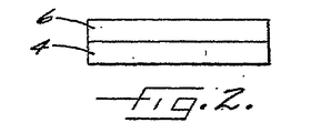
【解決手段】少なくとも直径約3インチ(75mm)と、4°オフ軸のウェハに対して、約500cm−2未満の底面転位密度を有する少なくとも1平方インチ(6.25cm2)の連続した表面領域とを有するSiCウェハであって、その製造方法は、3インチよりわずかに大きい直径を有するSiCブールを形成するステップと、0001平面に対して約2°と12°の間の角度で、該ブールをスライスして、ウェハにするステップであって、該ウェハは、各ウェハ上に、500cm−2未満の底面転位密度を有する少なくとも1平方インチの連続した表面領域を有する、ステップとを包含する。前記方法で背蔵した高品質シリコンカーバイド半導体前駆体ウェハ4は、追加的に、1つ以上の少なくとも一つのIII族窒化物層6を有する。
【選択図】図2
Description
本発明は、低欠陥シリコンカーバイドウェハおよび半導体用途のための前駆体としてのその使用と、大型高品質シリコンカーバイド単結晶のシード昇華成長とに関する。
一つの局面において、本発明は、SiCの高品質単結晶ウェハであり、該高品質単結晶ウェハは、少なくとも約3インチ(75mm)の直径と、約200cm−2未満の底面転位密度を有する少なくとも1平方インチ(6.25cm2)の連続した表面領域とを有する。
本発明は、高品質シリコンカーバイドウェハに関する。特に、本発明は、シード昇華を用いるこのようなウェハの成長を改善するための幾つかの技術を組み込んでいる。
Claims (1)
- 本願明細書に記載のSiCの高品質単結晶ウェハ。
Applications Claiming Priority (2)
| Application Number | Priority Date | Filing Date | Title |
|---|---|---|---|
| US11/147,645 US7294324B2 (en) | 2004-09-21 | 2005-06-08 | Low basal plane dislocation bulk grown SiC wafers |
| US11/147,645 | 2005-06-08 |
Related Parent Applications (1)
| Application Number | Title | Priority Date | Filing Date |
|---|---|---|---|
| JP2008514631A Division JP2008542181A (ja) | 2005-06-08 | 2006-04-05 | 低底面転位バルク成長SiCウェハ |
Publications (2)
| Publication Number | Publication Date |
|---|---|
| JP2010006699A true JP2010006699A (ja) | 2010-01-14 |
| JP5653598B2 JP5653598B2 (ja) | 2015-01-14 |
Family
ID=36659751
Family Applications (3)
| Application Number | Title | Priority Date | Filing Date |
|---|---|---|---|
| JP2008514631A Pending JP2008542181A (ja) | 2005-06-08 | 2006-04-05 | 低底面転位バルク成長SiCウェハ |
| JP2008184963A Pending JP2008290938A (ja) | 2005-06-08 | 2008-07-16 | 低底面転位バルク成長SiCウェハ |
| JP2009154425A Active JP5653598B2 (ja) | 2005-06-08 | 2009-06-29 | 低底面転位バルク成長SiCウェハ |
Family Applications Before (2)
| Application Number | Title | Priority Date | Filing Date |
|---|---|---|---|
| JP2008514631A Pending JP2008542181A (ja) | 2005-06-08 | 2006-04-05 | 低底面転位バルク成長SiCウェハ |
| JP2008184963A Pending JP2008290938A (ja) | 2005-06-08 | 2008-07-16 | 低底面転位バルク成長SiCウェハ |
Country Status (6)
| Country | Link |
|---|---|
| US (1) | US7294324B2 (ja) |
| EP (1) | EP1888821B1 (ja) |
| JP (3) | JP2008542181A (ja) |
| CN (1) | CN101194052B (ja) |
| TW (1) | TWI343423B (ja) |
| WO (1) | WO2006135476A1 (ja) |
Cited By (1)
| Publication number | Priority date | Publication date | Assignee | Title |
|---|---|---|---|---|
| JP2016149497A (ja) * | 2015-02-13 | 2016-08-18 | 住友電気工業株式会社 | 半導体装置 |
Families Citing this family (38)
| Publication number | Priority date | Publication date | Assignee | Title |
|---|---|---|---|---|
| JP4926556B2 (ja) * | 2006-06-20 | 2012-05-09 | 新日本製鐵株式会社 | 炭化珪素単結晶インゴットの製造方法及び炭化珪素単結晶基板 |
| US8410488B2 (en) * | 2006-09-14 | 2013-04-02 | Cree, Inc. | Micropipe-free silicon carbide and related method of manufacture |
| US8409351B2 (en) * | 2007-08-08 | 2013-04-02 | Sic Systems, Inc. | Production of bulk silicon carbide with hot-filament chemical vapor deposition |
| JP2010087397A (ja) * | 2008-10-02 | 2010-04-15 | Sumitomo Electric Ind Ltd | 炭化珪素半導体装置 |
| JP2010184833A (ja) * | 2009-02-12 | 2010-08-26 | Denso Corp | 炭化珪素単結晶基板および炭化珪素単結晶エピタキシャルウェハ |
| KR20120022964A (ko) | 2009-10-30 | 2012-03-12 | 스미토모덴키고교가부시키가이샤 | 탄화규소 기판의 제조 방법 및 탄화규소 기판 |
| CN102473594A (zh) | 2009-10-30 | 2012-05-23 | 住友电气工业株式会社 | 制造碳化硅衬底的方法和碳化硅衬底 |
| CA2781665A1 (en) | 2010-09-16 | 2012-03-22 | Sumitomo Electric Industries, Ltd. | Method for manufacturing semiconductor device |
| CN102534805B (zh) * | 2010-12-14 | 2014-08-06 | 北京天科合达蓝光半导体有限公司 | 一种碳化硅晶体退火工艺 |
| CN102560671B (zh) | 2010-12-31 | 2015-05-27 | 中国科学院物理研究所 | 半绝缘碳化硅单晶 |
| WO2013005347A1 (ja) | 2011-07-04 | 2013-01-10 | トヨタ自動車株式会社 | SiC単結晶及びその製造方法 |
| JP5614387B2 (ja) * | 2011-08-29 | 2014-10-29 | 新日鐵住金株式会社 | 炭化珪素単結晶の製造方法、及び炭化珪素単結晶インゴット |
| JP5696630B2 (ja) | 2011-09-21 | 2015-04-08 | 住友電気工業株式会社 | 炭化珪素基板およびその製造方法 |
| JP5750363B2 (ja) * | 2011-12-02 | 2015-07-22 | 株式会社豊田中央研究所 | SiC単結晶、SiCウェハ及び半導体デバイス |
| JP6226959B2 (ja) | 2012-04-20 | 2017-11-08 | トゥー‐シックス・インコーポレイテッド | 大口径高品質SiC単結晶、方法、及び装置 |
| US8860040B2 (en) | 2012-09-11 | 2014-10-14 | Dow Corning Corporation | High voltage power semiconductor devices on SiC |
| US9018639B2 (en) | 2012-10-26 | 2015-04-28 | Dow Corning Corporation | Flat SiC semiconductor substrate |
| US9797064B2 (en) | 2013-02-05 | 2017-10-24 | Dow Corning Corporation | Method for growing a SiC crystal by vapor deposition onto a seed crystal provided on a support shelf which permits thermal expansion |
| US9017804B2 (en) | 2013-02-05 | 2015-04-28 | Dow Corning Corporation | Method to reduce dislocations in SiC crystal growth |
| US9738991B2 (en) | 2013-02-05 | 2017-08-22 | Dow Corning Corporation | Method for growing a SiC crystal by vapor deposition onto a seed crystal provided on a supporting shelf which permits thermal expansion |
| JP5857986B2 (ja) | 2013-02-20 | 2016-02-10 | 株式会社デンソー | 炭化珪素単結晶および炭化珪素単結晶の製造方法 |
| JP6192948B2 (ja) * | 2013-02-20 | 2017-09-06 | 株式会社豊田中央研究所 | SiC単結晶、SiCウェハ、SiC基板、及び、SiCデバイス |
| US8940614B2 (en) | 2013-03-15 | 2015-01-27 | Dow Corning Corporation | SiC substrate with SiC epitaxial film |
| US9919972B2 (en) | 2013-05-02 | 2018-03-20 | Melior Innovations, Inc. | Pressed and self sintered polymer derived SiC materials, applications and devices |
| US10322936B2 (en) | 2013-05-02 | 2019-06-18 | Pallidus, Inc. | High purity polysilocarb materials, applications and processes |
| US11091370B2 (en) | 2013-05-02 | 2021-08-17 | Pallidus, Inc. | Polysilocarb based silicon carbide materials, applications and devices |
| US9657409B2 (en) | 2013-05-02 | 2017-05-23 | Melior Innovations, Inc. | High purity SiOC and SiC, methods compositions and applications |
| KR101933069B1 (ko) * | 2013-07-26 | 2018-12-27 | 투-식스 인코포레이티드 | 초고순도 탄화규소의 합성 방법 |
| WO2015035170A1 (en) * | 2013-09-06 | 2015-03-12 | Gtat Corporation | Bulk silicon carbide having low defect density |
| US9279192B2 (en) | 2014-07-29 | 2016-03-08 | Dow Corning Corporation | Method for manufacturing SiC wafer fit for integration with power device manufacturing technology |
| US10202706B2 (en) * | 2014-09-30 | 2019-02-12 | Showa Denko K.K. | Silicon carbide single crystal wafer and method of manufacturing a silicon carbide single crystal ingot |
| JP6592961B2 (ja) * | 2015-05-19 | 2019-10-23 | セイコーエプソン株式会社 | 炭化ケイ素基板および炭化ケイ素基板の製造方法 |
| US10020366B2 (en) * | 2015-09-25 | 2018-07-10 | The United States Of America, As Represented By The Secretary Of The Navy | Removal of basal plane dislocations from silicon carbide substrate surface by high temperature annealing and preserving surface morphology |
| JP6299827B2 (ja) * | 2016-09-07 | 2018-03-28 | 住友電気工業株式会社 | 半導体基板 |
| JP6832240B2 (ja) * | 2017-05-26 | 2021-02-24 | 昭和電工株式会社 | SiCエピタキシャルウェハ及びその製造方法 |
| JPWO2021149598A1 (ja) * | 2020-01-24 | 2021-07-29 | ||
| US20220189768A1 (en) * | 2020-12-15 | 2022-06-16 | Cree, Inc. | Large dimension silicon carbide single crystalline materials with reduced crystallographic stress |
| CN113652750B (zh) * | 2021-08-18 | 2022-07-12 | 山东天岳先进科技股份有限公司 | 具有环形形貌的碳化硅晶体及其制备方法和制得的衬底 |
Citations (4)
| Publication number | Priority date | Publication date | Assignee | Title |
|---|---|---|---|---|
| JPH11233391A (ja) * | 1998-02-12 | 1999-08-27 | Nippon Telegr & Teleph Corp <Ntt> | 結晶基板とそれを用いた半導体装置およびその製法 |
| JP2002261041A (ja) * | 2001-03-05 | 2002-09-13 | Shikusuon:Kk | SiC半導体のイオン注入層及びその製造方法 |
| JP2004099340A (ja) * | 2002-09-05 | 2004-04-02 | Nippon Steel Corp | 炭化珪素単結晶育成用種結晶と炭化珪素単結晶インゴット及びその製造方法 |
| JP2005351145A (ja) * | 2004-06-09 | 2005-12-22 | Toyota Motor Corp | 内燃機関の制御装置および制御方法 |
Family Cites Families (72)
| Publication number | Priority date | Publication date | Assignee | Title |
|---|---|---|---|---|
| NL87348C (ja) | 1954-03-19 | 1900-01-01 | ||
| US2938136A (en) * | 1958-08-26 | 1960-05-24 | Gen Electric | Electroluminescent lamp |
| US5373171A (en) * | 1987-03-12 | 1994-12-13 | Sumitomo Electric Industries, Ltd. | Thin film single crystal substrate |
| US4866005A (en) * | 1987-10-26 | 1989-09-12 | North Carolina State University | Sublimation of silicon carbide to produce large, device quality single crystals of silicon carbide |
| US4865685A (en) * | 1987-11-03 | 1989-09-12 | North Carolina State University | Dry etching of silicon carbide |
| GB8816632D0 (en) | 1988-07-13 | 1988-08-17 | Raychem Ltd | Electrical device |
| US5006914A (en) * | 1988-12-02 | 1991-04-09 | Advanced Technology Materials, Inc. | Single crystal semiconductor substrate articles and semiconductor devices comprising same |
| US5030583A (en) * | 1988-12-02 | 1991-07-09 | Advanced Technolgy Materials, Inc. | Method of making single crystal semiconductor substrate articles and semiconductor device |
| US5119540A (en) * | 1990-07-24 | 1992-06-09 | Cree Research, Inc. | Apparatus for eliminating residual nitrogen contamination in epitaxial layers of silicon carbide and resulting product |
| US5210051A (en) * | 1990-03-27 | 1993-05-11 | Cree Research, Inc. | High efficiency light emitting diodes from bipolar gallium nitride |
| JPH03295267A (ja) | 1990-04-13 | 1991-12-26 | Seiko Epson Corp | 薄膜装置 |
| US5311055A (en) * | 1991-11-22 | 1994-05-10 | The United States Of America As Represented By The Secretary Of The Navy | Trenched bipolar transistor structures |
| GB9206086D0 (en) | 1992-03-20 | 1992-05-06 | Philips Electronics Uk Ltd | Manufacturing electronic devices comprising,e.g.tfts and mims |
| DE4323814A1 (de) * | 1992-09-25 | 1994-03-31 | Siemens Ag | MIS-Feldeffekttransistor |
| US5709745A (en) * | 1993-01-25 | 1998-01-20 | Ohio Aerospace Institute | Compound semi-conductors and controlled doping thereof |
| US5611955A (en) * | 1993-10-18 | 1997-03-18 | Northrop Grumman Corp. | High resistivity silicon carbide substrates for high power microwave devices |
| US5422901A (en) * | 1993-11-15 | 1995-06-06 | Motorola, Inc. | Semiconductor device with high heat conductivity |
| US5393993A (en) * | 1993-12-13 | 1995-02-28 | Cree Research, Inc. | Buffer structure between silicon carbide and gallium nitride and resulting semiconductor devices |
| US5679152A (en) * | 1994-01-27 | 1997-10-21 | Advanced Technology Materials, Inc. | Method of making a single crystals Ga*N article |
| US5523589A (en) * | 1994-09-20 | 1996-06-04 | Cree Research, Inc. | Vertical geometry light emitting diode with group III nitride active layer and extended lifetime |
| US5563428A (en) * | 1995-01-30 | 1996-10-08 | Ek; Bruce A. | Layered structure of a substrate, a dielectric layer and a single crystal layer |
| US5661312A (en) * | 1995-03-30 | 1997-08-26 | Motorola | Silicon carbide MOSFET |
| US6670693B1 (en) * | 1996-12-05 | 2003-12-30 | Nathaniel R. Quick | Laser synthesized wide-bandgap semiconductor electronic devices and circuits |
| US5718760A (en) * | 1996-02-05 | 1998-02-17 | Cree Research, Inc. | Growth of colorless silicon carbide crystals |
| JP3384242B2 (ja) * | 1996-03-29 | 2003-03-10 | 株式会社豊田中央研究所 | 炭化珪素単結晶の製造方法 |
| US5872415A (en) * | 1996-08-16 | 1999-02-16 | Kobe Steel Usa Inc. | Microelectronic structures including semiconductor islands |
| US6533874B1 (en) * | 1996-12-03 | 2003-03-18 | Advanced Technology Materials, Inc. | GaN-based devices using thick (Ga, Al, In)N base layers |
| US6150239A (en) * | 1997-05-31 | 2000-11-21 | Max Planck Society | Method for the transfer of thin layers monocrystalline material onto a desirable substrate |
| US6201342B1 (en) * | 1997-06-30 | 2001-03-13 | The United States Of America As Represented By The Secretary Of The Navy | Automatically sharp field emission cathodes |
| TW358764B (en) * | 1997-07-07 | 1999-05-21 | Super Silicon Crystal Res Inst | A method of double-side lapping a wafer and an apparatus therefor |
| US6396864B1 (en) * | 1998-03-13 | 2002-05-28 | Jds Uniphase Corporation | Thermally conductive coatings for light emitting devices |
| US6316793B1 (en) * | 1998-06-12 | 2001-11-13 | Cree, Inc. | Nitride based transistors on semi-insulating silicon carbide substrates |
| WO2000004211A1 (de) * | 1998-07-13 | 2000-01-27 | Siemens Aktiengesellschaft | VERFAHREN ZUR ZÜCHTUNG VON SiC-EINKRISTALLEN |
| JP2000174166A (ja) * | 1998-10-02 | 2000-06-23 | Sumitomo Electric Ind Ltd | 半導体搭載パッケ―ジ |
| US6744800B1 (en) * | 1998-12-30 | 2004-06-01 | Xerox Corporation | Method and structure for nitride based laser diode arrays on an insulating substrate |
| US6396080B2 (en) * | 1999-05-18 | 2002-05-28 | Cree, Inc | Semi-insulating silicon carbide without vanadium domination |
| US6218680B1 (en) * | 1999-05-18 | 2001-04-17 | Cree, Inc. | Semi-insulating silicon carbide without vanadium domination |
| JP3314921B2 (ja) * | 1999-06-08 | 2002-08-19 | 三菱住友シリコン株式会社 | 半導体材料の切断・加工方法 |
| US6329088B1 (en) * | 1999-06-24 | 2001-12-11 | Advanced Technology Materials, Inc. | Silicon carbide epitaxial layers grown on substrates offcut towards <1{overscore (1)}00> |
| US6448642B1 (en) * | 2000-01-27 | 2002-09-10 | William W. Bewley | Pressure-bonded heat-sink system |
| US6586781B2 (en) * | 2000-02-04 | 2003-07-01 | Cree Lighting Company | Group III nitride based FETs and HEMTs with reduced trapping and method for producing the same |
| WO2001061765A1 (de) * | 2000-02-15 | 2001-08-23 | Osram Opto Semiconductors Gmbh | Strahlungsemittierendes halbleiterbauelement und verfahren zu dessen herstellung |
| US6599815B1 (en) * | 2000-06-30 | 2003-07-29 | Memc Electronic Materials, Inc. | Method and apparatus for forming a silicon wafer with a denuded zone |
| DE10032838B4 (de) * | 2000-07-06 | 2015-08-20 | Osram Opto Semiconductors Gmbh | Strahlung emittierender Halbleiterchip und Verfahren zu dessen Herstellung |
| FR2817395B1 (fr) * | 2000-11-27 | 2003-10-31 | Soitec Silicon On Insulator | Procede de fabrication d'un substrat notamment pour l'optique, l'electronique ou l'optoelectronique et substrat obtenu par ce procede |
| FR2835096B1 (fr) * | 2002-01-22 | 2005-02-18 | Procede de fabrication d'un substrat auto-porte en materiau semi-conducteur monocristallin | |
| WO2002044444A1 (en) * | 2000-11-30 | 2002-06-06 | Kyma Technologies, Inc. | Method and apparatus for producing miiin columns and miiin materials grown thereon |
| US6548333B2 (en) * | 2000-12-01 | 2003-04-15 | Cree, Inc. | Aluminum gallium nitride/gallium nitride high electron mobility transistors having a gate contact on a gallium nitride based cap segment |
| JP2002220299A (ja) * | 2001-01-19 | 2002-08-09 | Hoya Corp | 単結晶SiC及びその製造方法、SiC半導体装置並びにSiC複合材料 |
| US6497763B2 (en) * | 2001-01-19 | 2002-12-24 | The United States Of America As Represented By The Secretary Of The Navy | Electronic device with composite substrate |
| US6956250B2 (en) * | 2001-02-23 | 2005-10-18 | Nitronex Corporation | Gallium nitride materials including thermally conductive regions |
| US6699770B2 (en) * | 2001-03-01 | 2004-03-02 | John Tarje Torvik | Method of making a hybride substrate having a thin silicon carbide membrane layer |
| JP2002265296A (ja) | 2001-03-09 | 2002-09-18 | Kobe Steel Ltd | ダイヤモンド薄膜及びその製造方法 |
| US6686676B2 (en) * | 2001-04-30 | 2004-02-03 | General Electric Company | UV reflectors and UV-based light sources having reduced UV radiation leakage incorporating the same |
| US6849882B2 (en) * | 2001-05-11 | 2005-02-01 | Cree Inc. | Group-III nitride based high electron mobility transistor (HEMT) with barrier/spacer layer |
| US6507046B2 (en) * | 2001-05-11 | 2003-01-14 | Cree, Inc. | High-resistivity silicon carbide substrate for semiconductor devices with high break down voltage |
| US6706114B2 (en) * | 2001-05-21 | 2004-03-16 | Cree, Inc. | Methods of fabricating silicon carbide crystals |
| JP2003037074A (ja) | 2001-07-26 | 2003-02-07 | Toshiba Corp | 半導体装置およびその製造方法 |
| US6634770B2 (en) * | 2001-08-24 | 2003-10-21 | Densen Cao | Light source using semiconductor devices mounted on a heat sink |
| US6849874B2 (en) * | 2001-10-26 | 2005-02-01 | Cree, Inc. | Minimizing degradation of SiC bipolar semiconductor devices |
| US6670283B2 (en) * | 2001-11-20 | 2003-12-30 | International Business Machines Corporation | Backside protection films |
| US7030428B2 (en) * | 2001-12-03 | 2006-04-18 | Cree, Inc. | Strain balanced nitride heterojunction transistors |
| US6814801B2 (en) * | 2002-06-24 | 2004-11-09 | Cree, Inc. | Method for producing semi-insulating resistivity in high purity silicon carbide crystals |
| US7220313B2 (en) * | 2003-07-28 | 2007-05-22 | Cree, Inc. | Reducing nitrogen content in silicon carbide crystals by sublimation growth in a hydrogen-containing ambient |
| US7147715B2 (en) * | 2003-07-28 | 2006-12-12 | Cree, Inc. | Growth of ultra-high purity silicon carbide crystals in an ambient containing hydrogen |
| JP2005531153A (ja) * | 2002-06-26 | 2005-10-13 | ケンブリッジ セミコンダクター リミテッド | ラテラル半導体デバイス |
| US6964917B2 (en) * | 2003-04-08 | 2005-11-15 | Cree, Inc. | Semi-insulating silicon carbide produced by Neutron transmutation doping |
| CN1282770C (zh) * | 2003-12-24 | 2006-11-01 | 山东大学 | 一种生长具有半导体特性的大直径6H-SiC单晶的装置和方法 |
| EP1619276B1 (en) * | 2004-07-19 | 2017-01-11 | Norstel AB | Homoepitaxial growth of SiC on low off-axis SiC wafers |
| US7314520B2 (en) * | 2004-10-04 | 2008-01-01 | Cree, Inc. | Low 1c screw dislocation 3 inch silicon carbide wafer |
| US7314521B2 (en) | 2004-10-04 | 2008-01-01 | Cree, Inc. | Low micropipe 100 mm silicon carbide wafer |
| US7391058B2 (en) * | 2005-06-27 | 2008-06-24 | General Electric Company | Semiconductor devices and methods of making same |
-
2005
- 2005-06-08 US US11/147,645 patent/US7294324B2/en active Active
-
2006
- 2006-04-05 EP EP06749466.6A patent/EP1888821B1/en not_active Revoked
- 2006-04-05 WO PCT/US2006/012929 patent/WO2006135476A1/en active Application Filing
- 2006-04-05 JP JP2008514631A patent/JP2008542181A/ja active Pending
- 2006-04-05 CN CN2006800202948A patent/CN101194052B/zh active Active
- 2006-04-07 TW TW095112542A patent/TWI343423B/zh active
-
2008
- 2008-07-16 JP JP2008184963A patent/JP2008290938A/ja active Pending
-
2009
- 2009-06-29 JP JP2009154425A patent/JP5653598B2/ja active Active
Patent Citations (4)
| Publication number | Priority date | Publication date | Assignee | Title |
|---|---|---|---|---|
| JPH11233391A (ja) * | 1998-02-12 | 1999-08-27 | Nippon Telegr & Teleph Corp <Ntt> | 結晶基板とそれを用いた半導体装置およびその製法 |
| JP2002261041A (ja) * | 2001-03-05 | 2002-09-13 | Shikusuon:Kk | SiC半導体のイオン注入層及びその製造方法 |
| JP2004099340A (ja) * | 2002-09-05 | 2004-04-02 | Nippon Steel Corp | 炭化珪素単結晶育成用種結晶と炭化珪素単結晶インゴット及びその製造方法 |
| JP2005351145A (ja) * | 2004-06-09 | 2005-12-22 | Toyota Motor Corp | 内燃機関の制御装置および制御方法 |
Non-Patent Citations (1)
| Title |
|---|
| JPN6008044770; T. Kato et al.: 'Large diameter and long length growth of SiC single crystal' Mater. Sci. Forum Vol. 457-460, 2004, pp. 99-102, Trans Tech Publications * |
Cited By (1)
| Publication number | Priority date | Publication date | Assignee | Title |
|---|---|---|---|---|
| JP2016149497A (ja) * | 2015-02-13 | 2016-08-18 | 住友電気工業株式会社 | 半導体装置 |
Also Published As
| Publication number | Publication date |
|---|---|
| TW200700596A (en) | 2007-01-01 |
| US20060075958A1 (en) | 2006-04-13 |
| EP1888821B1 (en) | 2014-11-19 |
| CN101194052B (zh) | 2012-05-30 |
| CN101194052A (zh) | 2008-06-04 |
| JP2008290938A (ja) | 2008-12-04 |
| TWI343423B (en) | 2011-06-11 |
| WO2006135476A1 (en) | 2006-12-21 |
| JP5653598B2 (ja) | 2015-01-14 |
| US7294324B2 (en) | 2007-11-13 |
| JP2008542181A (ja) | 2008-11-27 |
| EP1888821A1 (en) | 2008-02-20 |
Similar Documents
| Publication | Publication Date | Title |
|---|---|---|
| JP5653598B2 (ja) | 低底面転位バルク成長SiCウェハ | |
| JP5680269B2 (ja) | 低マイクロパイプの100mm炭化ケイ素ウェハ | |
| US8785946B2 (en) | Low 1C screw dislocation 3 inch silicon carbide wafer | |
| US8410488B2 (en) | Micropipe-free silicon carbide and related method of manufacture |
Legal Events
| Date | Code | Title | Description |
|---|---|---|---|
| A521 | Request for written amendment filed |
Free format text: JAPANESE INTERMEDIATE CODE: A523 Effective date: 20100205 |
|
| RD04 | Notification of resignation of power of attorney |
Free format text: JAPANESE INTERMEDIATE CODE: A7424 Effective date: 20110124 |
|
| RD02 | Notification of acceptance of power of attorney |
Free format text: JAPANESE INTERMEDIATE CODE: A7422 Effective date: 20110112 |
|
| A131 | Notification of reasons for refusal |
Free format text: JAPANESE INTERMEDIATE CODE: A131 Effective date: 20120727 |
|
| A521 | Request for written amendment filed |
Free format text: JAPANESE INTERMEDIATE CODE: A523 Effective date: 20121025 |
|
| A131 | Notification of reasons for refusal |
Free format text: JAPANESE INTERMEDIATE CODE: A131 Effective date: 20121214 |
|
| A601 | Written request for extension of time |
Free format text: JAPANESE INTERMEDIATE CODE: A601 Effective date: 20130314 |
|
| A602 | Written permission of extension of time |
Free format text: JAPANESE INTERMEDIATE CODE: A602 Effective date: 20130319 |
|
| A521 | Request for written amendment filed |
Free format text: JAPANESE INTERMEDIATE CODE: A523 Effective date: 20130326 |
|
| A02 | Decision of refusal |
Free format text: JAPANESE INTERMEDIATE CODE: A02 Effective date: 20130531 |
|
| A521 | Request for written amendment filed |
Free format text: JAPANESE INTERMEDIATE CODE: A523 Effective date: 20130930 |
|
| A911 | Transfer to examiner for re-examination before appeal (zenchi) |
Free format text: JAPANESE INTERMEDIATE CODE: A911 Effective date: 20131007 |
|
| A912 | Re-examination (zenchi) completed and case transferred to appeal board |
Free format text: JAPANESE INTERMEDIATE CODE: A912 Effective date: 20131025 |
|
| A521 | Request for written amendment filed |
Free format text: JAPANESE INTERMEDIATE CODE: A523 Effective date: 20140829 |
|
| A61 | First payment of annual fees (during grant procedure) |
Free format text: JAPANESE INTERMEDIATE CODE: A61 Effective date: 20141119 |
|
| R150 | Certificate of patent or registration of utility model |
Ref document number: 5653598 Country of ref document: JP Free format text: JAPANESE INTERMEDIATE CODE: R150 |
|
| R250 | Receipt of annual fees |
Free format text: JAPANESE INTERMEDIATE CODE: R250 |
|
| R250 | Receipt of annual fees |
Free format text: JAPANESE INTERMEDIATE CODE: R250 |
|
| R250 | Receipt of annual fees |
Free format text: JAPANESE INTERMEDIATE CODE: R250 |
|
| R250 | Receipt of annual fees |
Free format text: JAPANESE INTERMEDIATE CODE: R250 |
|
| R250 | Receipt of annual fees |
Free format text: JAPANESE INTERMEDIATE CODE: R250 |
|
| R250 | Receipt of annual fees |
Free format text: JAPANESE INTERMEDIATE CODE: R250 |
|
| R250 | Receipt of annual fees |
Free format text: JAPANESE INTERMEDIATE CODE: R250 |