JP2008034851A - 超格子を有する半導体層構造 - Google Patents
超格子を有する半導体層構造 Download PDFInfo
- Publication number
- JP2008034851A JP2008034851A JP2007195432A JP2007195432A JP2008034851A JP 2008034851 A JP2008034851 A JP 2008034851A JP 2007195432 A JP2007195432 A JP 2007195432A JP 2007195432 A JP2007195432 A JP 2007195432A JP 2008034851 A JP2008034851 A JP 2008034851A
- Authority
- JP
- Japan
- Prior art keywords
- superlattice
- layer
- layers
- semiconductor layer
- layer structure
- Prior art date
- Legal status (The legal status is an assumption and is not a legal conclusion. Google has not performed a legal analysis and makes no representation as to the accuracy of the status listed.)
- Pending
Links
Images


Classifications
-
- H—ELECTRICITY
- H01—ELECTRIC ELEMENTS
- H01S—DEVICES USING THE PROCESS OF LIGHT AMPLIFICATION BY STIMULATED EMISSION OF RADIATION [LASER] TO AMPLIFY OR GENERATE LIGHT; DEVICES USING STIMULATED EMISSION OF ELECTROMAGNETIC RADIATION IN WAVE RANGES OTHER THAN OPTICAL
- H01S5/00—Semiconductor lasers
- H01S5/30—Structure or shape of the active region; Materials used for the active region
- H01S5/34—Structure or shape of the active region; Materials used for the active region comprising quantum well or superlattice structures, e.g. single quantum well [SQW] lasers, multiple quantum well [MQW] lasers or graded index separate confinement heterostructure [GRINSCH] lasers
- H01S5/343—Structure or shape of the active region; Materials used for the active region comprising quantum well or superlattice structures, e.g. single quantum well [SQW] lasers, multiple quantum well [MQW] lasers or graded index separate confinement heterostructure [GRINSCH] lasers in AIIIBV compounds, e.g. AlGaAs-laser, InP-based laser
- H01S5/34333—Structure or shape of the active region; Materials used for the active region comprising quantum well or superlattice structures, e.g. single quantum well [SQW] lasers, multiple quantum well [MQW] lasers or graded index separate confinement heterostructure [GRINSCH] lasers in AIIIBV compounds, e.g. AlGaAs-laser, InP-based laser with a well layer based on Ga(In)N or Ga(In)P, e.g. blue laser
-
- B—PERFORMING OPERATIONS; TRANSPORTING
- B82—NANOTECHNOLOGY
- B82Y—SPECIFIC USES OR APPLICATIONS OF NANOSTRUCTURES; MEASUREMENT OR ANALYSIS OF NANOSTRUCTURES; MANUFACTURE OR TREATMENT OF NANOSTRUCTURES
- B82Y20/00—Nanooptics, e.g. quantum optics or photonic crystals
-
- H—ELECTRICITY
- H01—ELECTRIC ELEMENTS
- H01L—SEMICONDUCTOR DEVICES NOT COVERED BY CLASS H10
- H01L33/00—Semiconductor devices with at least one potential-jump barrier or surface barrier specially adapted for light emission; Processes or apparatus specially adapted for the manufacture or treatment thereof or of parts thereof; Details thereof
- H01L33/02—Semiconductor devices with at least one potential-jump barrier or surface barrier specially adapted for light emission; Processes or apparatus specially adapted for the manufacture or treatment thereof or of parts thereof; Details thereof characterised by the semiconductor bodies
- H01L33/04—Semiconductor devices with at least one potential-jump barrier or surface barrier specially adapted for light emission; Processes or apparatus specially adapted for the manufacture or treatment thereof or of parts thereof; Details thereof characterised by the semiconductor bodies with a quantum effect structure or superlattice, e.g. tunnel junction
- H01L33/06—Semiconductor devices with at least one potential-jump barrier or surface barrier specially adapted for light emission; Processes or apparatus specially adapted for the manufacture or treatment thereof or of parts thereof; Details thereof characterised by the semiconductor bodies with a quantum effect structure or superlattice, e.g. tunnel junction within the light emitting region, e.g. quantum confinement structure or tunnel barrier
-
- H—ELECTRICITY
- H01—ELECTRIC ELEMENTS
- H01L—SEMICONDUCTOR DEVICES NOT COVERED BY CLASS H10
- H01L33/00—Semiconductor devices with at least one potential-jump barrier or surface barrier specially adapted for light emission; Processes or apparatus specially adapted for the manufacture or treatment thereof or of parts thereof; Details thereof
- H01L33/02—Semiconductor devices with at least one potential-jump barrier or surface barrier specially adapted for light emission; Processes or apparatus specially adapted for the manufacture or treatment thereof or of parts thereof; Details thereof characterised by the semiconductor bodies
- H01L33/26—Materials of the light emitting region
- H01L33/30—Materials of the light emitting region containing only elements of group III and group V of the periodic system
- H01L33/32—Materials of the light emitting region containing only elements of group III and group V of the periodic system containing nitrogen
-
- H—ELECTRICITY
- H01—ELECTRIC ELEMENTS
- H01L—SEMICONDUCTOR DEVICES NOT COVERED BY CLASS H10
- H01L2924/00—Indexing scheme for arrangements or methods for connecting or disconnecting semiconductor or solid-state bodies as covered by H01L24/00
- H01L2924/0001—Technical content checked by a classifier
- H01L2924/0002—Not covered by any one of groups H01L24/00, H01L24/00 and H01L2224/00
-
- H—ELECTRICITY
- H01—ELECTRIC ELEMENTS
- H01L—SEMICONDUCTOR DEVICES NOT COVERED BY CLASS H10
- H01L33/00—Semiconductor devices with at least one potential-jump barrier or surface barrier specially adapted for light emission; Processes or apparatus specially adapted for the manufacture or treatment thereof or of parts thereof; Details thereof
- H01L33/02—Semiconductor devices with at least one potential-jump barrier or surface barrier specially adapted for light emission; Processes or apparatus specially adapted for the manufacture or treatment thereof or of parts thereof; Details thereof characterised by the semiconductor bodies
- H01L33/04—Semiconductor devices with at least one potential-jump barrier or surface barrier specially adapted for light emission; Processes or apparatus specially adapted for the manufacture or treatment thereof or of parts thereof; Details thereof characterised by the semiconductor bodies with a quantum effect structure or superlattice, e.g. tunnel junction
-
- H—ELECTRICITY
- H01—ELECTRIC ELEMENTS
- H01S—DEVICES USING THE PROCESS OF LIGHT AMPLIFICATION BY STIMULATED EMISSION OF RADIATION [LASER] TO AMPLIFY OR GENERATE LIGHT; DEVICES USING STIMULATED EMISSION OF ELECTROMAGNETIC RADIATION IN WAVE RANGES OTHER THAN OPTICAL
- H01S5/00—Semiconductor lasers
- H01S5/04—Processes or apparatus for excitation, e.g. pumping, e.g. by electron beams
- H01S5/042—Electrical excitation ; Circuits therefor
- H01S5/0421—Electrical excitation ; Circuits therefor characterised by the semiconducting contacting layers
- H01S5/0422—Electrical excitation ; Circuits therefor characterised by the semiconducting contacting layers with n- and p-contacts on the same side of the active layer
-
- H—ELECTRICITY
- H01—ELECTRIC ELEMENTS
- H01S—DEVICES USING THE PROCESS OF LIGHT AMPLIFICATION BY STIMULATED EMISSION OF RADIATION [LASER] TO AMPLIFY OR GENERATE LIGHT; DEVICES USING STIMULATED EMISSION OF ELECTROMAGNETIC RADIATION IN WAVE RANGES OTHER THAN OPTICAL
- H01S5/00—Semiconductor lasers
- H01S5/20—Structure or shape of the semiconductor body to guide the optical wave ; Confining structures perpendicular to the optical axis, e.g. index or gain guiding, stripe geometry, broad area lasers, gain tailoring, transverse or lateral reflectors, special cladding structures, MQW barrier reflection layers
- H01S5/2004—Confining in the direction perpendicular to the layer structure
- H01S5/2009—Confining in the direction perpendicular to the layer structure by using electron barrier layers
-
- H—ELECTRICITY
- H01—ELECTRIC ELEMENTS
- H01S—DEVICES USING THE PROCESS OF LIGHT AMPLIFICATION BY STIMULATED EMISSION OF RADIATION [LASER] TO AMPLIFY OR GENERATE LIGHT; DEVICES USING STIMULATED EMISSION OF ELECTROMAGNETIC RADIATION IN WAVE RANGES OTHER THAN OPTICAL
- H01S5/00—Semiconductor lasers
- H01S5/30—Structure or shape of the active region; Materials used for the active region
- H01S5/305—Structure or shape of the active region; Materials used for the active region characterised by the doping materials used in the laser structure
- H01S5/3054—Structure or shape of the active region; Materials used for the active region characterised by the doping materials used in the laser structure p-doping
- H01S5/3063—Structure or shape of the active region; Materials used for the active region characterised by the doping materials used in the laser structure p-doping using Mg
-
- H—ELECTRICITY
- H01—ELECTRIC ELEMENTS
- H01S—DEVICES USING THE PROCESS OF LIGHT AMPLIFICATION BY STIMULATED EMISSION OF RADIATION [LASER] TO AMPLIFY OR GENERATE LIGHT; DEVICES USING STIMULATED EMISSION OF ELECTROMAGNETIC RADIATION IN WAVE RANGES OTHER THAN OPTICAL
- H01S5/00—Semiconductor lasers
- H01S5/30—Structure or shape of the active region; Materials used for the active region
- H01S5/32—Structure or shape of the active region; Materials used for the active region comprising PN junctions, e.g. hetero- or double- heterostructures
- H01S5/3211—Structure or shape of the active region; Materials used for the active region comprising PN junctions, e.g. hetero- or double- heterostructures characterised by special cladding layers, e.g. details on band-discontinuities
- H01S5/3213—Structure or shape of the active region; Materials used for the active region comprising PN junctions, e.g. hetero- or double- heterostructures characterised by special cladding layers, e.g. details on band-discontinuities asymmetric clading layers
-
- H—ELECTRICITY
- H01—ELECTRIC ELEMENTS
- H01S—DEVICES USING THE PROCESS OF LIGHT AMPLIFICATION BY STIMULATED EMISSION OF RADIATION [LASER] TO AMPLIFY OR GENERATE LIGHT; DEVICES USING STIMULATED EMISSION OF ELECTROMAGNETIC RADIATION IN WAVE RANGES OTHER THAN OPTICAL
- H01S5/00—Semiconductor lasers
- H01S5/30—Structure or shape of the active region; Materials used for the active region
- H01S5/32—Structure or shape of the active region; Materials used for the active region comprising PN junctions, e.g. hetero- or double- heterostructures
- H01S5/3211—Structure or shape of the active region; Materials used for the active region comprising PN junctions, e.g. hetero- or double- heterostructures characterised by special cladding layers, e.g. details on band-discontinuities
- H01S5/3215—Structure or shape of the active region; Materials used for the active region comprising PN junctions, e.g. hetero- or double- heterostructures characterised by special cladding layers, e.g. details on band-discontinuities graded composition cladding layers
-
- H—ELECTRICITY
- H01—ELECTRIC ELEMENTS
- H01S—DEVICES USING THE PROCESS OF LIGHT AMPLIFICATION BY STIMULATED EMISSION OF RADIATION [LASER] TO AMPLIFY OR GENERATE LIGHT; DEVICES USING STIMULATED EMISSION OF ELECTROMAGNETIC RADIATION IN WAVE RANGES OTHER THAN OPTICAL
- H01S5/00—Semiconductor lasers
- H01S5/30—Structure or shape of the active region; Materials used for the active region
- H01S5/32—Structure or shape of the active region; Materials used for the active region comprising PN junctions, e.g. hetero- or double- heterostructures
- H01S5/3211—Structure or shape of the active region; Materials used for the active region comprising PN junctions, e.g. hetero- or double- heterostructures characterised by special cladding layers, e.g. details on band-discontinuities
- H01S5/3216—Structure or shape of the active region; Materials used for the active region comprising PN junctions, e.g. hetero- or double- heterostructures characterised by special cladding layers, e.g. details on band-discontinuities quantum well or superlattice cladding layers
-
- H—ELECTRICITY
- H01—ELECTRIC ELEMENTS
- H01S—DEVICES USING THE PROCESS OF LIGHT AMPLIFICATION BY STIMULATED EMISSION OF RADIATION [LASER] TO AMPLIFY OR GENERATE LIGHT; DEVICES USING STIMULATED EMISSION OF ELECTROMAGNETIC RADIATION IN WAVE RANGES OTHER THAN OPTICAL
- H01S5/00—Semiconductor lasers
- H01S5/30—Structure or shape of the active region; Materials used for the active region
- H01S5/32—Structure or shape of the active region; Materials used for the active region comprising PN junctions, e.g. hetero- or double- heterostructures
- H01S5/3211—Structure or shape of the active region; Materials used for the active region comprising PN junctions, e.g. hetero- or double- heterostructures characterised by special cladding layers, e.g. details on band-discontinuities
- H01S5/3218—Structure or shape of the active region; Materials used for the active region comprising PN junctions, e.g. hetero- or double- heterostructures characterised by special cladding layers, e.g. details on band-discontinuities specially strained cladding layers, other than for strain compensation
Abstract
【解決手段】超格子内の異なるタイプの隣接する層は、少なくとも1つの元素の組成において異なっており、超格子内で、同じタイプの少なくとも2つの層は少なくとも1つの元素の異なる含有量を有しており、該少なくとも1つの元素の含有量は超格子の層内で勾配状であり、超格子の層は所定の濃度でドーピング材料を含んでおり、当該超格子は、異なるドーピング材料でドープされた層を有している半導体層構造、およびこのような半導体層構造を有するオプトエレクトロニクスデバイス。
【選択図】図1
Description
この超格子9は、交互に積み重ねられた、第1のタイプaの層9aと第2のタイプbの層9bとを有する。
この構造をある程度、2つの層タイプのみを有するGaN/AlGaN超格子としてみることもできる。ここではAlGaN層は階段関数によって勾配状にされている。前述したように、1つの層内の勾配状のAl含有量は超格子の導電性を高める効果を支持している。
Claims (15)
- 半導体層構造であって、
該半導体層構造は超格子(9)を有しており、該超格子は、第1のタイプ(a)と少なくとも1つの第2のタイプ(b)の積み重ねられた層(9a,9b)から成り、
・前記第1のタイプ(a)と少なくとも1つの第2のタイプ(b)の層(9a,9b)はIII−V族化合物半導体であり、
・超格子(9)内の異なるタイプの隣接する層は、少なくとも1つの元素の組成において異なっており、
・超格子(9)内で、同じタイプの少なくとも2つの層は、少なくとも1つの元素の異なる含有量(CAl,CIn)を有しており、
・該少なくとも1つの元素の含有量(CAl,CIn)は、超格子(9)の層(9a,9b)内で勾配状であり、
・超格子(9)の層(9a、9b)は所定の濃度でドーピング材料を含んでおり、当該超格子(9)は、異なるドーピング材料でドープされた層(9a,9b)を有している、
ことを特徴とする半導体層構造。 - 前記超格子(9)は、交互に積み重ねられたInxAlyGa1-x-yN層及びInwAlzGa1-w-zN層を有しており、式中0≦x、y、w、z≦1及びx+y≦1およびw+z≦1である、請求項1記載の半導体層構造。
- 前記超格子(9)は、交互に積み重ねられたInxAlyGa1-x-yP層及びInwAlzGa1-w-zP層を有しており、式中0≦x、y、w、z≦1であるか、または交互に積層されたInxAlyGa1-x-yAs層及びInwAlzGa1-w-zAs層を有しており、式中0≦x、y、w、z≦1及びx+y≦1及びw+z≦1である、請求項1記載の半導体層構造。
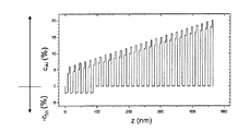
- 前記超格子(9)の個々の層に半導体層構造内の垂直位置(z)が割り当てられており、層内の前記少なくとも1つの元素の含有量(CAl,CIn)は、所定のように、半導体層構造内の自身の垂直位置(z)に依存している、請求項1から3までのいずれか1項記載の半導体層構造。
- 前記垂直位置(z)に対する少なくとも1つの元素の含有量(CAl,CIn)の依存性は、超格子(9)の全ての層(9a,9b)に対して、共通の関数によって設定されている、請求項4記載の半導体層構造。
- 前記垂直位置(z)に対する少なくとも1つの元素の含有量(CAl,CIn)の依存性は、第1のタイプ(a)の層(9a)に対しては第1の関数によって設定されており、少なくとも1つの第2のタイプ(b)の層(9b)に対しては少なくとも1つの第2の関数によって定められている、請求項4記載の半導体層構造。
- 前記第1の関数および/または少なくとも1つの第2の関数および/または共通の関数は、階段関数または単調増加関数/減少関数または一次関数または多項式関数または指数関数または対数関数または周期関数またはこれらの関数を重ね合わせたものであるか、またはこれらの関数の一部を有している、請求項5または6記載の半導体層構造。
- 前記少なくとも1つの元素の含有量(CAl,CIn)は、超格子(9)の1つの層(9a、9b)内で一定である、請求項1から7までのいずれか1項記載の半導体層構造。
- 全ての層(9a、9b)は同じ厚さを有している、請求項1から8までのいずれか1項記載の半導体層構造。
- 異なるタイプ(a、b)の層(9a、9b)は異なる厚さを有している、請求項1から8までのいずれか1項記載の半導体層構造。
- 請求項1から10までのいずれか1項に記載された半導体層構造を有している、
ことを特徴とするオプトエレクトロニクスデバイス。 - 光学活性層(6)を有しており、同じタイプの少なくとも2つの層において含有量(CAl)が異なっている少なくとも1つの元素はAlであり、半導体層構造の超格子(9)内のAl含有量(CAl)は、当該光学活性層(6)からの距離が増すとともに上昇する、請求項11記載のオプトエレクトロニクスデバイス。
- 光学活性層(6)を有しており、同じタイプの少なくとも2つの層において含有量(CAl)が異なっている少なくとも1つの元素はAlであり、半導体層構造の超格子(9)内のAl含有量(CAl)は、当該光学活性層(6)からの距離が増すとともに低下する、請求項11記載のオプトエレクトロニクスデバイス。
- 発光ダイオードである、請求項11から13までのいずれか1項記載のオプトエレクトロニクスデバイス。
- レーザーダイオードである、請求項11から13までのいずれか1項記載のオプトエレクトロニクスデバイス。
Applications Claiming Priority (2)
| Application Number | Priority Date | Filing Date | Title |
|---|---|---|---|
| DE102006034820 | 2006-07-27 | ||
| DE102006046237A DE102006046237A1 (de) | 2006-07-27 | 2006-09-29 | Halbleiter-Schichtstruktur mit Übergitter |
Publications (2)
| Publication Number | Publication Date |
|---|---|
| JP2008034851A true JP2008034851A (ja) | 2008-02-14 |
| JP2008034851A5 JP2008034851A5 (ja) | 2011-06-23 |
Family
ID=38542049
Family Applications (1)
| Application Number | Title | Priority Date | Filing Date |
|---|---|---|---|
| JP2007195432A Pending JP2008034851A (ja) | 2006-07-27 | 2007-07-27 | 超格子を有する半導体層構造 |
Country Status (3)
| Country | Link |
|---|---|
| US (2) | US7893424B2 (ja) |
| EP (1) | EP1883141B1 (ja) |
| JP (1) | JP2008034851A (ja) |
Cited By (6)
| Publication number | Priority date | Publication date | Assignee | Title |
|---|---|---|---|---|
| WO2010055635A1 (ja) * | 2008-11-13 | 2010-05-20 | パナソニック株式会社 | 窒化物半導体デバイス |
| US7822089B2 (en) | 2006-07-27 | 2010-10-26 | Osram Opto Semiconductors Gmbh | Semiconductor layer structure with superlattice |
| US7893424B2 (en) | 2006-07-27 | 2011-02-22 | Osram Opto Semiconductors Gmbh | Semiconductor layer structure with superlattice |
| US8022392B2 (en) | 2006-07-27 | 2011-09-20 | Osram Opto Semiconductors Gmbh | Semiconductor layer structure with superlattice |
| KR20120045049A (ko) * | 2009-08-13 | 2012-05-08 | 오스람 옵토 세미컨덕터스 게엠베하 | 전기적으로 펌핑된 광전자 반도체 칩 |
| JP2014143338A (ja) * | 2013-01-25 | 2014-08-07 | Sharp Corp | 窒化物半導体発光素子 |
Families Citing this family (42)
| Publication number | Priority date | Publication date | Assignee | Title |
|---|---|---|---|---|
| US20060039498A1 (en) * | 2004-08-19 | 2006-02-23 | De Figueiredo Rui J P | Pre-distorter for orthogonal frequency division multiplexing systems and method of operating the same |
| US8563995B2 (en) * | 2008-03-27 | 2013-10-22 | Nitek, Inc. | Ultraviolet light emitting diode/laser diode with nested superlattice |
| DE102008030584A1 (de) | 2008-06-27 | 2009-12-31 | Osram Opto Semiconductors Gmbh | Verfahren zur Herstellung eines optoelektronischen Bauelementes und optoelektronisches Bauelement |
| US9297093B2 (en) * | 2009-09-28 | 2016-03-29 | Tokuyama Corporation | Layered body having a single crystal layer |
| US8389977B2 (en) | 2009-12-10 | 2013-03-05 | Transphorm Inc. | Reverse side engineered III-nitride devices |
| JP5060656B2 (ja) * | 2009-12-21 | 2012-10-31 | 株式会社東芝 | 窒化物半導体発光素子およびその製造方法 |
| DE102009060749B4 (de) | 2009-12-30 | 2021-12-30 | OSRAM Opto Semiconductors Gesellschaft mit beschränkter Haftung | Optoelektronischer Halbleiterchip |
| FR2957718B1 (fr) * | 2010-03-16 | 2012-04-20 | Commissariat Energie Atomique | Diode electroluminescente hybride a rendement eleve |
| US8742460B2 (en) | 2010-12-15 | 2014-06-03 | Transphorm Inc. | Transistors with isolation regions |
| US8643062B2 (en) | 2011-02-02 | 2014-02-04 | Transphorm Inc. | III-N device structures and methods |
| US8358673B2 (en) * | 2011-02-17 | 2013-01-22 | Corning Incorporated | Strain balanced laser diode |
| EP2681816A1 (en) * | 2011-02-28 | 2014-01-08 | Corning Incorporated | Semiconductor lasers with indium containing cladding layers |
| US8901604B2 (en) | 2011-09-06 | 2014-12-02 | Transphorm Inc. | Semiconductor devices with guard rings |
| US9257547B2 (en) | 2011-09-13 | 2016-02-09 | Transphorm Inc. | III-N device structures having a non-insulating substrate |
| US8598937B2 (en) | 2011-10-07 | 2013-12-03 | Transphorm Inc. | High power semiconductor electronic components with increased reliability |
| KR20130079873A (ko) * | 2012-01-03 | 2013-07-11 | 엘지이노텍 주식회사 | 발광소자 및 이를 포함하는 조명시스템 |
| CN102544281A (zh) * | 2012-01-20 | 2012-07-04 | 厦门市三安光电科技有限公司 | 具有多层势垒结构的氮化镓基发光二极管 |
| US9165766B2 (en) * | 2012-02-03 | 2015-10-20 | Transphorm Inc. | Buffer layer structures suited for III-nitride devices with foreign substrates |
| US9093366B2 (en) | 2012-04-09 | 2015-07-28 | Transphorm Inc. | N-polar III-nitride transistors |
| US9219189B2 (en) | 2012-09-14 | 2015-12-22 | Palo Alto Research Center Incorporated | Graded electron blocking layer |
| US9401452B2 (en) | 2012-09-14 | 2016-07-26 | Palo Alto Research Center Incorporated | P-side layers for short wavelength light emitters |
| KR101936312B1 (ko) * | 2012-10-09 | 2019-01-08 | 엘지이노텍 주식회사 | 발광소자 |
| KR102042181B1 (ko) * | 2012-10-22 | 2019-11-07 | 엘지이노텍 주식회사 | 발광소자 |
| US9087718B2 (en) | 2013-03-13 | 2015-07-21 | Transphorm Inc. | Enhancement-mode III-nitride devices |
| US9245992B2 (en) | 2013-03-15 | 2016-01-26 | Transphorm Inc. | Carbon doping semiconductor devices |
| KR20140117117A (ko) * | 2013-03-26 | 2014-10-07 | 인텔렉추얼디스커버리 주식회사 | 질화물 반도체 발광소자 |
| WO2015009514A1 (en) | 2013-07-19 | 2015-01-22 | Transphorm Inc. | Iii-nitride transistor including a p-type depleting layer |
| US9318593B2 (en) | 2014-07-21 | 2016-04-19 | Transphorm Inc. | Forming enhancement mode III-nitride devices |
| KR102237111B1 (ko) * | 2014-07-28 | 2021-04-08 | 엘지이노텍 주식회사 | 발광소자 및 조명시스템 |
| FR3028670B1 (fr) * | 2014-11-18 | 2017-12-22 | Commissariat Energie Atomique | Structure semi-conductrice a couche de semi-conducteur du groupe iii-v ou ii-vi comprenant une structure cristalline a mailles cubiques ou hexagonales |
| US9536966B2 (en) | 2014-12-16 | 2017-01-03 | Transphorm Inc. | Gate structures for III-N devices |
| US9536967B2 (en) | 2014-12-16 | 2017-01-03 | Transphorm Inc. | Recessed ohmic contacts in a III-N device |
| TWI577046B (zh) * | 2014-12-23 | 2017-04-01 | 錼創科技股份有限公司 | 半導體發光元件及其製作方法 |
| US9673352B2 (en) * | 2015-04-30 | 2017-06-06 | National Chiao Tung University | Semiconductor light emitting device |
| CN108604597B (zh) | 2016-01-15 | 2021-09-17 | 创世舫电子有限公司 | 具有al(1-x)sixo栅极绝缘体的增强模式iii-氮化物器件 |
| TWI762486B (zh) | 2016-05-31 | 2022-05-01 | 美商創世舫科技有限公司 | 包含漸變空乏層的三族氮化物裝置 |
| DE102017119931A1 (de) * | 2017-08-30 | 2019-02-28 | Osram Opto Semiconductors Gmbh | Optoelektronisches Halbleiterbauelement |
| US10516076B2 (en) | 2018-02-01 | 2019-12-24 | Silanna UV Technologies Pte Ltd | Dislocation filter for semiconductor devices |
| US10879420B2 (en) | 2018-07-09 | 2020-12-29 | University Of Iowa Research Foundation | Cascaded superlattice LED system |
| CN110600591B (zh) * | 2019-08-21 | 2021-11-26 | 苏州紫灿科技有限公司 | 具有啁啾超晶格最终势垒结构的深紫外led及制备方法 |
| CN114503381A (zh) * | 2019-09-30 | 2022-05-13 | 恩耐公司 | 用于优化有源区应变和改善激光二极管性能的被应变设计的包覆层 |
| US11322647B2 (en) | 2020-05-01 | 2022-05-03 | Silanna UV Technologies Pte Ltd | Buried contact layer for UV emitting device |
Citations (7)
| Publication number | Priority date | Publication date | Assignee | Title |
|---|---|---|---|---|
| JPH10223983A (ja) * | 1997-02-04 | 1998-08-21 | Nichia Chem Ind Ltd | 窒化物半導体素子 |
| JPH11251684A (ja) * | 1998-02-26 | 1999-09-17 | Nichia Chem Ind Ltd | 窒化物半導体素子 |
| JPH11340505A (ja) * | 1998-05-25 | 1999-12-10 | Matsushita Electric Ind Co Ltd | 窒化ガリウム系化合物半導体発光素子 |
| JP2002057410A (ja) * | 2000-05-29 | 2002-02-22 | Fuji Photo Film Co Ltd | 半導体レーザ素子 |
| JP2002314129A (ja) * | 2001-03-29 | 2002-10-25 | Lumileds Lighting Us Llc | Iii族窒化物デバイスのための窒化ガリウムインジウム平滑構造 |
| WO2003085790A1 (fr) * | 2002-04-04 | 2003-10-16 | Sharp Kabushiki Kaisha | Dispositif laser a semi-conducteur |
| JP2003318495A (ja) * | 2002-04-23 | 2003-11-07 | Mitsubishi Electric Corp | 傾斜状多重量子バリアを用いた半導体発光素子 |
Family Cites Families (68)
| Publication number | Priority date | Publication date | Assignee | Title |
|---|---|---|---|---|
| JPS60145686A (ja) | 1984-01-09 | 1985-08-01 | Nec Corp | 半導体レ−ザ |
| US4882734A (en) | 1988-03-09 | 1989-11-21 | Xerox Corporation | Quantum well heterostructure lasers with low current density threshold and higher TO values |
| US4839899A (en) * | 1988-03-09 | 1989-06-13 | Xerox Corporation | Wavelength tuning of multiple quantum well (MQW) heterostructure lasers |
| JPH01241192A (ja) | 1988-03-23 | 1989-09-26 | Fujitsu Ltd | 半導体装置 |
| US4961197A (en) | 1988-09-07 | 1990-10-02 | Hitachi, Ltd. | Semiconductor laser device |
| CA1299719C (en) | 1989-01-13 | 1992-04-28 | Hui Chun Liu | Semiconductor superlattice infrared source |
| US5060028A (en) | 1989-01-19 | 1991-10-22 | Hewlett-Packard Company | High band-gap opto-electronic device |
| US4984242A (en) * | 1989-09-18 | 1991-01-08 | Spectra Diode Laboratories, Inc. | GaAs/AlGaAs heterostructure laser containing indium |
| US5319657A (en) | 1991-10-08 | 1994-06-07 | Matsushita Electric Industrial Co., Ltd. | Semiconductor laser of modulation doping quantum well structure with stopper against dopant dispersion and manufacturing method thereof |
| US5198682A (en) | 1991-11-12 | 1993-03-30 | Hughes Aircraft Company | Multiple quantum well superlattice infrared detector with graded conductive band |
| JPH0794829A (ja) | 1993-04-05 | 1995-04-07 | Matsushita Electric Ind Co Ltd | 半導体レーザ |
| US5395793A (en) | 1993-12-23 | 1995-03-07 | National Research Council Of Canada | Method of bandgap tuning of semiconductor quantum well structures |
| US5570386A (en) | 1994-04-04 | 1996-10-29 | Lucent Technologies Inc. | Semiconductor laser |
| US5497012A (en) | 1994-06-15 | 1996-03-05 | Hewlett-Packard Company | Unipolar band minima devices |
| EP1473781A3 (en) | 1994-07-21 | 2007-02-21 | Matsushita Electric Industrial Co., Ltd. | Semiconductor light-emitting device and production method thereof |
| US5670798A (en) | 1995-03-29 | 1997-09-23 | North Carolina State University | Integrated heterostructures of Group III-V nitride semiconductor materials including epitaxial ohmic contact non-nitride buffer layer and methods of fabricating same |
| US5588015A (en) | 1995-08-22 | 1996-12-24 | University Of Houston | Light emitting devices based on interband transitions in type-II quantum well heterostructures |
| JPH1022524A (ja) | 1996-07-02 | 1998-01-23 | Omron Corp | 半導体発光素子 |
| US5936989A (en) | 1997-04-29 | 1999-08-10 | Lucent Technologies, Inc. | Quantum cascade laser |
| KR100644933B1 (ko) | 1997-01-09 | 2006-11-15 | 니치아 카가쿠 고교 가부시키가이샤 | 질화물반도체소자 |
| US6677619B1 (en) | 1997-01-09 | 2004-01-13 | Nichia Chemical Industries, Ltd. | Nitride semiconductor device |
| JP3014339B2 (ja) * | 1997-04-25 | 2000-02-28 | カナレ電気株式会社 | 量子波干渉層を有した半導体素子 |
| JP3642157B2 (ja) | 1997-05-26 | 2005-04-27 | ソニー株式会社 | p型III族ナイトライド化合物半導体、発光ダイオードおよび半導体レーザ |
| WO1999005728A1 (en) | 1997-07-25 | 1999-02-04 | Nichia Chemical Industries, Ltd. | Nitride semiconductor device |
| JPH1168158A (ja) | 1997-08-20 | 1999-03-09 | Sanyo Electric Co Ltd | 窒化ガリウム系化合物半導体装置 |
| JP2000091708A (ja) | 1998-09-14 | 2000-03-31 | Toshiba Corp | 半導体発光素子 |
| JP2000286451A (ja) | 1998-11-17 | 2000-10-13 | Nichia Chem Ind Ltd | 窒化物半導体素子 |
| JP2000244070A (ja) | 1999-02-19 | 2000-09-08 | Sony Corp | 半導体装置および半導体発光素子 |
| WO2000058999A2 (en) | 1999-03-26 | 2000-10-05 | Matsushita Electric Industrial Co., Ltd. | Semiconductor structures having a strain compensated layer and method of fabrication |
| GB9913950D0 (en) | 1999-06-15 | 1999-08-18 | Arima Optoelectronics Corp | Unipolar light emitting devices based on iii-nitride semiconductor superlattices |
| DE19955747A1 (de) * | 1999-11-19 | 2001-05-23 | Osram Opto Semiconductors Gmbh | Optische Halbleitervorrichtung mit Mehrfach-Quantentopf-Struktur |
| US6441393B2 (en) | 1999-11-17 | 2002-08-27 | Lumileds Lighting U.S., Llc | Semiconductor devices with selectively doped III-V nitride layers |
| JP2001168385A (ja) | 1999-12-06 | 2001-06-22 | Toyoda Gosei Co Ltd | Iii族窒化物系化合物半導体素子及びiii族窒化物系化合物半導体発光素子 |
| US6535536B2 (en) | 2000-04-10 | 2003-03-18 | Fuji Photo Film Co., Ltd. | Semiconductor laser element |
| US6556604B1 (en) | 2000-11-08 | 2003-04-29 | Lucent Technologies Inc. | Flat minibands with spatially symmetric wavefunctions in intersubband superlattice light emitters |
| JP3453558B2 (ja) | 2000-12-25 | 2003-10-06 | 松下電器産業株式会社 | 窒化物半導体素子 |
| EP1385241B1 (en) | 2001-03-28 | 2008-12-31 | Nichia Corporation | Nitride semiconductor element |
| US6649942B2 (en) | 2001-05-23 | 2003-11-18 | Sanyo Electric Co., Ltd. | Nitride-based semiconductor light-emitting device |
| US6630692B2 (en) | 2001-05-29 | 2003-10-07 | Lumileds Lighting U.S., Llc | III-Nitride light emitting devices with low driving voltage |
| US6958497B2 (en) | 2001-05-30 | 2005-10-25 | Cree, Inc. | Group III nitride based light emitting diode structures with a quantum well and superlattice, group III nitride based quantum well structures and group III nitride based superlattice structures |
| US7692182B2 (en) | 2001-05-30 | 2010-04-06 | Cree, Inc. | Group III nitride based quantum well light emitting device structures with an indium containing capping structure |
| JP2003008058A (ja) | 2001-06-18 | 2003-01-10 | Showa Denko Kk | AlGaInPエピタキシャルウエーハ及びそれを製造する方法並びにそれを用いた半導体発光素子 |
| JP4057802B2 (ja) | 2001-09-05 | 2008-03-05 | 株式会社日立製作所 | 半導体光素子 |
| TWI275220B (en) | 2001-11-05 | 2007-03-01 | Nichia Corp | Nitride semiconductor device |
| US6618413B2 (en) | 2001-12-21 | 2003-09-09 | Xerox Corporation | Graded semiconductor layers for reducing threshold voltage for a nitride-based laser diode structure |
| US7919791B2 (en) | 2002-03-25 | 2011-04-05 | Cree, Inc. | Doped group III-V nitride materials, and microelectronic devices and device precursor structures comprising same |
| GB0207307D0 (en) | 2002-03-27 | 2002-05-08 | Koninkl Philips Electronics Nv | In-pixel memory for display devices |
| JP3755084B2 (ja) | 2002-04-24 | 2006-03-15 | 中東産業株式会社 | 蝶番 |
| JP4221697B2 (ja) | 2002-06-17 | 2009-02-12 | 日本電気株式会社 | 半導体装置 |
| US20030235224A1 (en) | 2002-06-19 | 2003-12-25 | Ohlander Ulf Roald | Strained quantum-well structure having ternary-alloy material in both quantum-well layers and barrier layers |
| US20060139743A1 (en) | 2002-11-20 | 2006-06-29 | Marsh John H | Semiconductor optical device with beam focusing |
| GB0306279D0 (en) | 2003-03-19 | 2003-04-23 | Bookham Technology Plc | High power semiconductor laser with large optical superlattice waveguide |
| TW200505063A (en) * | 2003-07-10 | 2005-02-01 | Nichia Corp | Nitride semiconductor laser element |
| KR100580623B1 (ko) | 2003-08-04 | 2006-05-16 | 삼성전자주식회사 | 초격자 구조의 반도체층을 갖는 반도체 소자 및 그 제조방법 |
| TWI228320B (en) | 2003-09-09 | 2005-02-21 | Ind Tech Res Inst | An avalanche photo-detector(APD) with high saturation power, high gain-bandwidth product |
| US20070290230A1 (en) | 2003-09-25 | 2007-12-20 | Yasutoshi Kawaguchi | Nitride Semiconductor Device And Production Method Thereof |
| US20050162616A1 (en) * | 2004-01-23 | 2005-07-28 | Hewlett-Packard Co. | System and method of contrast enhancement in digital projectors |
| DE102004009531B4 (de) | 2004-02-20 | 2007-03-01 | Forschungszentrum Rossendorf E.V. | Quanten-Kaskaden-Laser-Struktur |
| US7294868B2 (en) | 2004-06-25 | 2007-11-13 | Finisar Corporation | Super lattice tunnel junctions |
| KR100662191B1 (ko) | 2004-12-23 | 2006-12-27 | 엘지이노텍 주식회사 | 질화물 반도체 발광소자 및 그 제조방법 |
| US7885306B2 (en) * | 2006-06-30 | 2011-02-08 | Osram Opto Semiconductors Gmbh | Edge-emitting semiconductor laser chip |
| DE102006046237A1 (de) | 2006-07-27 | 2008-01-31 | Osram Opto Semiconductors Gmbh | Halbleiter-Schichtstruktur mit Übergitter |
| DE102006046228A1 (de) * | 2006-07-27 | 2008-01-31 | Osram Opto Semiconductors Gmbh | Halbleiter-Schichtstruktur mit Übergitter |
| EP1883141B1 (de) * | 2006-07-27 | 2017-05-24 | OSRAM Opto Semiconductors GmbH | LD oder LED mit Übergitter-Mantelschicht |
| PL1883119T3 (pl) | 2006-07-27 | 2016-04-29 | Osram Opto Semiconductors Gmbh | Półprzewodnikowa struktura warstwowa z supersiecią |
| EP1883140B1 (de) * | 2006-07-27 | 2013-02-27 | OSRAM Opto Semiconductors GmbH | LD oder LED mit Übergitter-Mantelschicht und Dotierungsgradienten |
| US7547908B2 (en) * | 2006-12-22 | 2009-06-16 | Philips Lumilieds Lighting Co, Llc | III-nitride light emitting devices grown on templates to reduce strain |
| DE102010009457A1 (de) * | 2010-02-26 | 2011-09-01 | Osram Opto Semiconductors Gmbh | Optoelektronischer Halbleiterchip |
-
2007
- 2007-07-13 EP EP07013822.7A patent/EP1883141B1/de not_active Expired - Fee Related
- 2007-07-20 US US11/780,514 patent/US7893424B2/en not_active Expired - Fee Related
- 2007-07-27 JP JP2007195432A patent/JP2008034851A/ja active Pending
-
2011
- 2011-01-19 US US13/009,422 patent/US8471240B2/en active Active
Patent Citations (7)
| Publication number | Priority date | Publication date | Assignee | Title |
|---|---|---|---|---|
| JPH10223983A (ja) * | 1997-02-04 | 1998-08-21 | Nichia Chem Ind Ltd | 窒化物半導体素子 |
| JPH11251684A (ja) * | 1998-02-26 | 1999-09-17 | Nichia Chem Ind Ltd | 窒化物半導体素子 |
| JPH11340505A (ja) * | 1998-05-25 | 1999-12-10 | Matsushita Electric Ind Co Ltd | 窒化ガリウム系化合物半導体発光素子 |
| JP2002057410A (ja) * | 2000-05-29 | 2002-02-22 | Fuji Photo Film Co Ltd | 半導体レーザ素子 |
| JP2002314129A (ja) * | 2001-03-29 | 2002-10-25 | Lumileds Lighting Us Llc | Iii族窒化物デバイスのための窒化ガリウムインジウム平滑構造 |
| WO2003085790A1 (fr) * | 2002-04-04 | 2003-10-16 | Sharp Kabushiki Kaisha | Dispositif laser a semi-conducteur |
| JP2003318495A (ja) * | 2002-04-23 | 2003-11-07 | Mitsubishi Electric Corp | 傾斜状多重量子バリアを用いた半導体発光素子 |
Cited By (11)
| Publication number | Priority date | Publication date | Assignee | Title |
|---|---|---|---|---|
| US7822089B2 (en) | 2006-07-27 | 2010-10-26 | Osram Opto Semiconductors Gmbh | Semiconductor layer structure with superlattice |
| US7893424B2 (en) | 2006-07-27 | 2011-02-22 | Osram Opto Semiconductors Gmbh | Semiconductor layer structure with superlattice |
| US20110168977A1 (en) * | 2006-07-27 | 2011-07-14 | Osram Opto Semiconductors Gmbh, A Germany Corporation | Semiconductor layer structure with superlattice |
| US8022392B2 (en) | 2006-07-27 | 2011-09-20 | Osram Opto Semiconductors Gmbh | Semiconductor layer structure with superlattice |
| US8471240B2 (en) | 2006-07-27 | 2013-06-25 | Osram Opto Semiconductors Gmbh | Semiconductor layer structure with superlattice |
| WO2010055635A1 (ja) * | 2008-11-13 | 2010-05-20 | パナソニック株式会社 | 窒化物半導体デバイス |
| JP2010118559A (ja) * | 2008-11-13 | 2010-05-27 | Panasonic Corp | 窒化物半導体デバイス |
| US8816366B2 (en) | 2008-11-13 | 2014-08-26 | Panasonic Corporation | Nitride semiconductor device |
| KR20120045049A (ko) * | 2009-08-13 | 2012-05-08 | 오스람 옵토 세미컨덕터스 게엠베하 | 전기적으로 펌핑된 광전자 반도체 칩 |
| KR101682345B1 (ko) | 2009-08-13 | 2016-12-05 | 오스람 옵토 세미컨덕터스 게엠베하 | 전기적으로 펌핑된 광전자 반도체 칩 |
| JP2014143338A (ja) * | 2013-01-25 | 2014-08-07 | Sharp Corp | 窒化物半導体発光素子 |
Also Published As
| Publication number | Publication date |
|---|---|
| US8471240B2 (en) | 2013-06-25 |
| US20110168977A1 (en) | 2011-07-14 |
| US7893424B2 (en) | 2011-02-22 |
| US20080054247A1 (en) | 2008-03-06 |
| EP1883141B1 (de) | 2017-05-24 |
| EP1883141A1 (de) | 2008-01-30 |
Similar Documents
| Publication | Publication Date | Title |
|---|---|---|
| JP2008034851A (ja) | 超格子を有する半導体層構造 | |
| JP5156290B2 (ja) | オプトエレクトロニクスデバイス | |
| JP6259611B2 (ja) | 短波長発光素子のためのp側層 | |
| US10361343B2 (en) | Ultraviolet light emitting diodes | |
| JP5735984B2 (ja) | 発光半導体チップ | |
| JP2007081180A (ja) | 半導体発光素子 | |
| KR20160065178A (ko) | 양극 알루미늄 산화물 층을 포함하는 헤테로구조체 | |
| KR20070081184A (ko) | 질화물계 반도체 발광소자 및 그 제조방법 | |
| US9214595B2 (en) | Semiconductor light emitting device | |
| JP2016048785A (ja) | 電流拡散層を有する発光ダイオードチップ | |
| JP5430829B2 (ja) | 超格子を有する半導体層構造およびオプトエレクトロニクスデバイス | |
| TW201937753A (zh) | 氮化物半導體發光元件 | |
| US20160072015A1 (en) | Vertical ultraviolet light emitting device and method for manufacturing the same | |
| KR101368687B1 (ko) | 초격자 구조를 이용한 질화물계 반도체 발광 소자의 제조 방법 | |
| KR101303589B1 (ko) | 질화물계 반도체 발광 소자 및 그의 제조 방법 | |
| CN111108658B (zh) | 激光二极管 | |
| KR101216342B1 (ko) | 질화물계 반도체 발광 소자 | |
| KR20090103855A (ko) | 질화물계 반도체 발광소자 및 그 제조방법 | |
| US10218152B1 (en) | Semiconductor laser diode with low threshold current | |
| JP6785221B2 (ja) | 半導体発光素子 | |
| JP2004349485A (ja) | レーザダイオード素子 | |
| JP2013041960A (ja) | 半導体レーザ装置 | |
| KR20110037620A (ko) | 반도체 발광소자에 표면 플라즈몬 공명 구조를 형성시키는 방법 | |
| KR20140133662A (ko) | 투명 전극을 포함하는 발광 소자 및 그 제조 방법 |
Legal Events
| Date | Code | Title | Description |
|---|---|---|---|
| A621 | Written request for application examination |
Free format text: JAPANESE INTERMEDIATE CODE: A621 Effective date: 20100427 |
|
| RD04 | Notification of resignation of power of attorney |
Free format text: JAPANESE INTERMEDIATE CODE: A7424 Effective date: 20101227 |
|
| RD04 | Notification of resignation of power of attorney |
Free format text: JAPANESE INTERMEDIATE CODE: A7424 Effective date: 20101228 |
|
| A521 | Request for written amendment filed |
Free format text: JAPANESE INTERMEDIATE CODE: A523 Effective date: 20110502 |
|
| A977 | Report on retrieval |
Free format text: JAPANESE INTERMEDIATE CODE: A971007 Effective date: 20120411 |
|
| A131 | Notification of reasons for refusal |
Free format text: JAPANESE INTERMEDIATE CODE: A131 Effective date: 20120412 |
|
| A601 | Written request for extension of time |
Free format text: JAPANESE INTERMEDIATE CODE: A601 Effective date: 20120712 |
|
| A602 | Written permission of extension of time |
Free format text: JAPANESE INTERMEDIATE CODE: A602 Effective date: 20120718 |
|
| A521 | Request for written amendment filed |
Free format text: JAPANESE INTERMEDIATE CODE: A523 Effective date: 20120810 |
|
| A02 | Decision of refusal |
Free format text: JAPANESE INTERMEDIATE CODE: A02 Effective date: 20130104 |