JP5735984B2 - 発光半導体チップ - Google Patents
発光半導体チップ Download PDFInfo
- Publication number
- JP5735984B2 JP5735984B2 JP2012546427A JP2012546427A JP5735984B2 JP 5735984 B2 JP5735984 B2 JP 5735984B2 JP 2012546427 A JP2012546427 A JP 2012546427A JP 2012546427 A JP2012546427 A JP 2012546427A JP 5735984 B2 JP5735984 B2 JP 5735984B2
- Authority
- JP
- Japan
- Prior art keywords
- doping
- type conductive
- multilayer structure
- semiconductor
- semiconductor chip
- Prior art date
- Legal status (The legal status is an assumption and is not a legal conclusion. Google has not performed a legal analysis and makes no representation as to the accuracy of the status listed.)
- Active
Links
- 239000004065 semiconductor Substances 0.000 title claims description 142
- 230000005855 radiation Effects 0.000 claims description 26
- 239000000463 material Substances 0.000 claims description 18
- 230000004888 barrier function Effects 0.000 claims description 14
- -1 nitride compound Chemical class 0.000 claims description 8
- 239000000758 substrate Substances 0.000 claims description 7
- 239000013078 crystal Substances 0.000 claims description 6
- 239000002800 charge carrier Substances 0.000 description 11
- 229910052738 indium Inorganic materials 0.000 description 11
- APFVFJFRJDLVQX-UHFFFAOYSA-N indium atom Chemical compound [In] APFVFJFRJDLVQX-UHFFFAOYSA-N 0.000 description 10
- 238000000151 deposition Methods 0.000 description 9
- 230000008021 deposition Effects 0.000 description 9
- 238000002347 injection Methods 0.000 description 5
- 239000007924 injection Substances 0.000 description 5
- 239000010409 thin film Substances 0.000 description 5
- XUIMIQQOPSSXEZ-UHFFFAOYSA-N Silicon Chemical compound [Si] XUIMIQQOPSSXEZ-UHFFFAOYSA-N 0.000 description 4
- 239000000203 mixture Substances 0.000 description 4
- 229910052710 silicon Inorganic materials 0.000 description 4
- 239000010703 silicon Substances 0.000 description 4
- 230000003595 spectral effect Effects 0.000 description 4
- 229910052782 aluminium Inorganic materials 0.000 description 3
- 238000009826 distribution Methods 0.000 description 3
- 238000000059 patterning Methods 0.000 description 3
- 239000000126 substance Substances 0.000 description 3
- 229910002601 GaN Inorganic materials 0.000 description 2
- PXHVJJICTQNCMI-UHFFFAOYSA-N Nickel Chemical compound [Ni] PXHVJJICTQNCMI-UHFFFAOYSA-N 0.000 description 2
- KDLHZDBZIXYQEI-UHFFFAOYSA-N Palladium Chemical compound [Pd] KDLHZDBZIXYQEI-UHFFFAOYSA-N 0.000 description 2
- BQCADISMDOOEFD-UHFFFAOYSA-N Silver Chemical compound [Ag] BQCADISMDOOEFD-UHFFFAOYSA-N 0.000 description 2
- XAGFODPZIPBFFR-UHFFFAOYSA-N aluminium Chemical compound [Al] XAGFODPZIPBFFR-UHFFFAOYSA-N 0.000 description 2
- 230000001427 coherent effect Effects 0.000 description 2
- 238000011161 development Methods 0.000 description 2
- 230000018109 developmental process Effects 0.000 description 2
- 239000002019 doping agent Substances 0.000 description 2
- PCHJSUWPFVWCPO-UHFFFAOYSA-N gold Chemical compound [Au] PCHJSUWPFVWCPO-UHFFFAOYSA-N 0.000 description 2
- 229910052737 gold Inorganic materials 0.000 description 2
- 239000010931 gold Substances 0.000 description 2
- 238000004519 manufacturing process Methods 0.000 description 2
- 238000005259 measurement Methods 0.000 description 2
- 229910052751 metal Inorganic materials 0.000 description 2
- 239000002184 metal Substances 0.000 description 2
- 238000002488 metal-organic chemical vapour deposition Methods 0.000 description 2
- BASFCYQUMIYNBI-UHFFFAOYSA-N platinum Chemical compound [Pt] BASFCYQUMIYNBI-UHFFFAOYSA-N 0.000 description 2
- 238000013139 quantization Methods 0.000 description 2
- 230000035945 sensitivity Effects 0.000 description 2
- 229910052709 silver Inorganic materials 0.000 description 2
- 239000004332 silver Substances 0.000 description 2
- JBRZTFJDHDCESZ-UHFFFAOYSA-N AsGa Chemical compound [As]#[Ga] JBRZTFJDHDCESZ-UHFFFAOYSA-N 0.000 description 1
- VYZAMTAEIAYCRO-UHFFFAOYSA-N Chromium Chemical compound [Cr] VYZAMTAEIAYCRO-UHFFFAOYSA-N 0.000 description 1
- RYGMFSIKBFXOCR-UHFFFAOYSA-N Copper Chemical compound [Cu] RYGMFSIKBFXOCR-UHFFFAOYSA-N 0.000 description 1
- 229910001218 Gallium arsenide Inorganic materials 0.000 description 1
- JMASRVWKEDWRBT-UHFFFAOYSA-N Gallium nitride Chemical compound [Ga]#N JMASRVWKEDWRBT-UHFFFAOYSA-N 0.000 description 1
- 229910000629 Rh alloy Inorganic materials 0.000 description 1
- 239000000853 adhesive Substances 0.000 description 1
- 230000001070 adhesive effect Effects 0.000 description 1
- 229910045601 alloy Inorganic materials 0.000 description 1
- 239000000956 alloy Substances 0.000 description 1
- 239000012876 carrier material Substances 0.000 description 1
- 239000000919 ceramic Substances 0.000 description 1
- 229910052804 chromium Inorganic materials 0.000 description 1
- 239000011651 chromium Substances 0.000 description 1
- 150000001875 compounds Chemical class 0.000 description 1
- 229910052802 copper Inorganic materials 0.000 description 1
- 239000010949 copper Substances 0.000 description 1
- PMHQVHHXPFUNSP-UHFFFAOYSA-M copper(1+);methylsulfanylmethane;bromide Chemical compound Br[Cu].CSC PMHQVHHXPFUNSP-UHFFFAOYSA-M 0.000 description 1
- 230000001419 dependent effect Effects 0.000 description 1
- 238000010586 diagram Methods 0.000 description 1
- 238000009792 diffusion process Methods 0.000 description 1
- 238000000605 extraction Methods 0.000 description 1
- 229910052733 gallium Inorganic materials 0.000 description 1
- 229910052732 germanium Inorganic materials 0.000 description 1
- GNPVGFCGXDBREM-UHFFFAOYSA-N germanium atom Chemical compound [Ge] GNPVGFCGXDBREM-UHFFFAOYSA-N 0.000 description 1
- 238000007373 indentation Methods 0.000 description 1
- 229910001092 metal group alloy Inorganic materials 0.000 description 1
- 150000002739 metals Chemical class 0.000 description 1
- 229910052759 nickel Inorganic materials 0.000 description 1
- 229910052757 nitrogen Inorganic materials 0.000 description 1
- 229910052763 palladium Inorganic materials 0.000 description 1
- 230000000704 physical effect Effects 0.000 description 1
- 229910052697 platinum Inorganic materials 0.000 description 1
- 239000002096 quantum dot Substances 0.000 description 1
- 230000006798 recombination Effects 0.000 description 1
- 238000005215 recombination Methods 0.000 description 1
- 238000002310 reflectometry Methods 0.000 description 1
- 239000010948 rhodium Substances 0.000 description 1
- MHOVAHRLVXNVSD-UHFFFAOYSA-N rhodium atom Chemical compound [Rh] MHOVAHRLVXNVSD-UHFFFAOYSA-N 0.000 description 1
- 229910052594 sapphire Inorganic materials 0.000 description 1
- 239000010980 sapphire Substances 0.000 description 1
- HBMJWWWQQXIZIP-UHFFFAOYSA-N silicon carbide Chemical compound [Si+]#[C-] HBMJWWWQQXIZIP-UHFFFAOYSA-N 0.000 description 1
- 229910010271 silicon carbide Inorganic materials 0.000 description 1
- 229910000679 solder Inorganic materials 0.000 description 1
- 238000003892 spreading Methods 0.000 description 1
- 238000005309 stochastic process Methods 0.000 description 1
- 238000003860 storage Methods 0.000 description 1
Images


Classifications
-
- H01L33/04—
-
- H01L33/06—
-
- H01L33/0093—
-
- H01L33/14—
-
- H01L33/24—
-
- H01L33/32—
-
- H01L33/382—
-
- H—ELECTRICITY
- H01—ELECTRIC ELEMENTS
- H01L—SEMICONDUCTOR DEVICES NOT COVERED BY CLASS H10
- H01L2224/00—Indexing scheme for arrangements for connecting or disconnecting semiconductor or solid-state bodies and methods related thereto as covered by H01L24/00
- H01L2224/01—Means for bonding being attached to, or being formed on, the surface to be connected, e.g. chip-to-package, die-attach, "first-level" interconnects; Manufacturing methods related thereto
- H01L2224/10—Bump connectors; Manufacturing methods related thereto
- H01L2224/15—Structure, shape, material or disposition of the bump connectors after the connecting process
- H01L2224/16—Structure, shape, material or disposition of the bump connectors after the connecting process of an individual bump connector
- H01L2224/161—Disposition
- H01L2224/16151—Disposition the bump connector connecting between a semiconductor or solid-state body and an item not being a semiconductor or solid-state body, e.g. chip-to-substrate, chip-to-passive
- H01L2224/16221—Disposition the bump connector connecting between a semiconductor or solid-state body and an item not being a semiconductor or solid-state body, e.g. chip-to-substrate, chip-to-passive the body and the item being stacked
- H01L2224/16225—Disposition the bump connector connecting between a semiconductor or solid-state body and an item not being a semiconductor or solid-state body, e.g. chip-to-substrate, chip-to-passive the body and the item being stacked the item being non-metallic, e.g. insulating substrate with or without metallisation
-
- H—ELECTRICITY
- H01—ELECTRIC ELEMENTS
- H01L—SEMICONDUCTOR DEVICES NOT COVERED BY CLASS H10
- H01L2924/00—Indexing scheme for arrangements or methods for connecting or disconnecting semiconductor or solid-state bodies as covered by H01L24/00
- H01L2924/0001—Technical content checked by a classifier
- H01L2924/0002—Not covered by any one of groups H01L24/00, H01L24/00 and H01L2224/00
-
- H01L33/22—
Description
− 活性領域を有する半導体積層体(特にエピタキシャル積層体)を備えた半導体ボディの第1の主面(キャリア要素の側の面)に、ミラー層が堆積または形成されており(例えば、ブラッグミラーとして半導体層に組み込まれている)、このミラー層は、半導体積層体において生成された放射の少なくとも一部分を反射して半導体積層体に戻す。
− 半導体積層体の厚さは、20μm以下の範囲、特に10μm以下の範囲である。
− 半導体積層体は、少なくとも一面が混合構造(intermixing structure)である少なくとも1層の半導体層を含んでおり、この混合構造によって、理想的には半導体積層体における近似的に光のエルゴード分布につながり、すなわち、この混合構造は、実質的にエルゴード的確率過程である散乱挙動を示す。
本特許出願は、独国特許出願第102009060747.1号の優先権を主張し、この文書の開示内容は参照によって本出願に組み込まれている。
Claims (12)
- 半導体積層体を有する半導体ボディ(2)を備えた半導体チップ(1)であって、
− 前記半導体積層体が、n型導電多層構造(21)と、p型導電半導体層(22)と、放射を生成するための活性領域(20)と、を備えており、前記活性領域が前記n型導電多層構造と前記p型導電半導体層との間に配置されており、
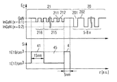
− 前記n型導電多層構造が、複数の井戸層(211)を有する量子構造を備えており、前記複数の井戸層が、障壁層(212)の間に配置されており、
− 少なくとも1つのドーピングピーク(4)を備えたドーピングプロファイルが、前記n型導電多層構造に形成されており、
− 前記n型導電多層構造が、前記ドーピングピークに隣接する領域を備えており、前記ドーピングピークに隣接する前記領域においては、前記井戸層と前記井戸層に隣接する障壁層とが低濃度にドープされており、
− 前記ドーピングプロファイルがさらなるドーピングピーク(41)を備えており、前記n型導電多層構造の少なくとも1層の井戸層が、前記ドーピングピークと前記さらなるドーピングピークとの間に配置されており、
− 前記n型導電多層構造の前記量子構造のサブ領域(216)が、前記さらなるドーピングピーク(41)によって高いドーピング濃度を備えている、
半導体チップ(1)。 - 前記少なくとも1つのドーピングピークにおけるドーピング濃度が、前記n型導電多層構造の、n型導電性に低濃度にドープされた領域(45)、におけるドーピング濃度の少なくとも5倍である、
請求項1に記載の半導体チップ。 - 前記少なくとも1つのドーピングピークにおけるドーピング濃度が少なくとも4×10¹⁸/cm3であり、n型導電性に低濃度にドープされた前記領域におけるドーピング濃度が最大で8×1017/cm3である、
請求項2に記載の半導体チップ。 - 前記ドーピングピークの垂直方向の大きさが、1nm〜30nmの範囲内(両端値を含む)である、
請求項1から請求項3のいずれかに記載の半導体チップ。 - 前記ドーピングピークの垂直方向の大きさが、5nm〜20nmの範囲内(両端値を含む)である、
請求項1から請求項4のいずれかに記載の半導体チップ。 - 前記活性領域から前記ドーピングピークまでの距離が、2nm〜20nmの範囲内(両端値を含む)である、
請求項1から請求項5のいずれかに記載の半導体チップ。 - 前記活性領域が複数の井戸層(201)を備えており、前記ドーピングピークが、前記n型導電多層構造の前記井戸層のうち前記活性領域に最も近い前記井戸層と、前記活性領域の前記井戸層のうち前記n型導電多層構造に最も近い前記井戸層との間に配置されている、
請求項1から請求項6のいずれかに記載の半導体チップ。 - 前記n型導電多層構造の前記井戸層のバンドギャップが、前記活性領域の前記井戸層(201)のバンドギャップと少なくとも同じ大きさである、
請求項7に記載の半導体チップ。 - 前記活性領域が窒化物化合物半導体材料をベースとする、
請求項1から請求項8のいずれかに記載の半導体チップ。 - 前記n型導電多層構造の結晶構造が、V形状の凹部を備えている、
請求項1から請求項9のいずれかに記載の半導体チップ。 - 前記半導体積層体の成長基板が前記半導体ボディから除去されている、
請求項1から請求項10のいずれかに記載の半導体チップ。 - − 前記少なくとも1つのドーピングピークにおけるドーピング濃度が、前記ドーピングピークに隣接している、前記n型導電多層構造の領域、におけるドーピング濃度の少なくとも5倍であり、
− 前記活性領域が、少なくとも1層の井戸層(201)を有する量子構造、を備えており、
− 前記n型導電多層構造の前記井戸層のバンドギャップが、前記活性領域の前記井戸層のバンドギャップよりも大きい、
請求項1に記載の半導体チップ。
Applications Claiming Priority (3)
| Application Number | Priority Date | Filing Date | Title |
|---|---|---|---|
| DE102009060747A DE102009060747A1 (de) | 2009-12-30 | 2009-12-30 | Halbleiterchip |
| DE102009060747.1 | 2009-12-30 | ||
| PCT/EP2010/070761 WO2011080249A1 (de) | 2009-12-30 | 2010-12-27 | Lichtemittierender halbleiterchip |
Publications (3)
| Publication Number | Publication Date |
|---|---|
| JP2013516751A JP2013516751A (ja) | 2013-05-13 |
| JP2013516751A5 JP2013516751A5 (ja) | 2014-02-20 |
| JP5735984B2 true JP5735984B2 (ja) | 2015-06-17 |
Family
ID=43827573
Family Applications (1)
| Application Number | Title | Priority Date | Filing Date |
|---|---|---|---|
| JP2012546427A Active JP5735984B2 (ja) | 2009-12-30 | 2010-12-27 | 発光半導体チップ |
Country Status (8)
| Country | Link |
|---|---|
| US (4) | US9012885B2 (ja) |
| EP (1) | EP2519980B1 (ja) |
| JP (1) | JP5735984B2 (ja) |
| KR (3) | KR20170080718A (ja) |
| CN (2) | CN106229395B (ja) |
| DE (1) | DE102009060747A1 (ja) |
| TW (1) | TWI449212B (ja) |
| WO (1) | WO2011080249A1 (ja) |
Families Citing this family (15)
| Publication number | Priority date | Publication date | Assignee | Title |
|---|---|---|---|---|
| DE102009060747A1 (de) | 2009-12-30 | 2011-07-07 | OSRAM Opto Semiconductors GmbH, 93055 | Halbleiterchip |
| US8357924B2 (en) | 2010-01-05 | 2013-01-22 | Seoul Opto Device Co., Ltd. | Light emitting diode and method of fabricating the same |
| DE102011100037A1 (de) | 2011-04-29 | 2012-10-31 | Osram Opto Semiconductors Gmbh | Strahlung emittierender Halbleiterchip mit integriertem ESD-Schutz |
| JP5123414B2 (ja) * | 2011-05-16 | 2013-01-23 | 株式会社東芝 | 半導体発光素子、窒化物半導体ウェーハ及び窒化物半導体層の製造方法 |
| US9070613B2 (en) * | 2011-09-07 | 2015-06-30 | Lg Innotek Co., Ltd. | Light emitting device |
| DE102013103602A1 (de) * | 2013-04-10 | 2014-10-16 | Osram Opto Semiconductors Gmbh | Optoelektronischer Halbleiterchip und Verfahren zu seiner Herstellung |
| DE102013104272A1 (de) | 2013-04-26 | 2014-10-30 | Osram Opto Semiconductors Gmbh | Optoelektronisches Bauelement und Verfahren zu seiner Herstellung |
| DE102014111058A1 (de) * | 2014-08-04 | 2016-02-04 | Osram Opto Semiconductors Gmbh | Optoelektronisches Bauelement und Verfahren zur Herstellung |
| CN104701431B (zh) * | 2014-11-27 | 2017-03-29 | 厦门市三安光电科技有限公司 | 一种发光二极管的外延结构及其制作方法 |
| KR102391513B1 (ko) | 2015-10-05 | 2022-04-27 | 삼성전자주식회사 | 물질막 적층체, 발광 소자, 발광 패키지, 및 발광 소자의 제조 방법 |
| US20180033912A1 (en) * | 2016-07-28 | 2018-02-01 | Lumileds Llc | Iii-p light emitting device with a superlattice |
| JP6921179B2 (ja) * | 2016-07-28 | 2021-08-18 | ルミレッズ リミテッド ライアビリティ カンパニー | 超格子を用いたiii−p発光デバイス |
| DE102016120419A1 (de) * | 2016-10-26 | 2018-04-26 | Osram Opto Semiconductors Gmbh | Halbleiterkörper |
| DE102016123262A1 (de) * | 2016-12-01 | 2018-06-07 | Osram Opto Semiconductors Gmbh | Strahlungsemittierender Halbleiterkörper und Verfahren zur Herstellung einer Halbleiterschichtenfolge |
| DE102017104370A1 (de) * | 2017-03-02 | 2018-09-06 | Osram Opto Semiconductors Gmbh | Halbleiterkörper |
Family Cites Families (40)
| Publication number | Priority date | Publication date | Assignee | Title |
|---|---|---|---|---|
| JPH07263748A (ja) * | 1994-03-22 | 1995-10-13 | Toyoda Gosei Co Ltd | 3族窒化物半導体発光素子及びその製造方法 |
| US6677619B1 (en) * | 1997-01-09 | 2004-01-13 | Nichia Chemical Industries, Ltd. | Nitride semiconductor device |
| JP3374737B2 (ja) | 1997-01-09 | 2003-02-10 | 日亜化学工業株式会社 | 窒化物半導体素子 |
| JP3429446B2 (ja) | 1998-03-19 | 2003-07-22 | シャープ株式会社 | 半導体発光素子 |
| EP0908988A3 (en) | 1997-10-06 | 2001-10-17 | Sharp Kabushiki Kaisha | Light-emitting device and fabricating method thereof |
| US7193246B1 (en) | 1998-03-12 | 2007-03-20 | Nichia Corporation | Nitride semiconductor device |
| JP3622562B2 (ja) | 1998-03-12 | 2005-02-23 | 日亜化学工業株式会社 | 窒化物半導体発光ダイオード |
| JP4629178B2 (ja) | 1998-10-06 | 2011-02-09 | 日亜化学工業株式会社 | 窒化物半導体素子 |
| US6649942B2 (en) * | 2001-05-23 | 2003-11-18 | Sanyo Electric Co., Ltd. | Nitride-based semiconductor light-emitting device |
| US6717969B2 (en) * | 2001-07-16 | 2004-04-06 | Fuji Photo Film Co., Ltd. | Semiconductor laser device which includes current confinement structure and trenches formed through current stopping layer down to active layer |
| KR100909739B1 (ko) | 2002-01-28 | 2009-07-29 | 니치아 카가쿠 고교 가부시키가이샤 | 대향전극구조의 질화물 반도체소자 |
| SG115549A1 (en) * | 2002-07-08 | 2005-10-28 | Sumitomo Chemical Co | Epitaxial substrate for compound semiconductor light emitting device, method for producing the same and light emitting device |
| JP2005093682A (ja) * | 2003-09-17 | 2005-04-07 | Toyoda Gosei Co Ltd | GaN系半導体発光素子及びその製造方法 |
| KR100456063B1 (ko) | 2004-02-13 | 2004-11-10 | 에피밸리 주식회사 | Ⅲ-질화물 반도체 발광소자 |
| JP2005277374A (ja) * | 2004-02-26 | 2005-10-06 | Toyoda Gosei Co Ltd | Iii族窒化物系化合物半導体発光素子及びその製造方法 |
| CN1324719C (zh) | 2004-04-01 | 2007-07-04 | 光磊科技股份有限公司 | 一种发光二极管 |
| TWI250666B (en) | 2004-05-03 | 2006-03-01 | Osram Opto Semiconductors Gmbh | Method to produce a radiation-emitting semiconductor-chip and said produced semiconductor-chip |
| US7943949B2 (en) * | 2004-09-09 | 2011-05-17 | Bridgelux, Inc. | III-nitride based on semiconductor device with low-resistance ohmic contacts |
| US7042018B2 (en) * | 2004-09-22 | 2006-05-09 | Formosa Epitaxy Incorporation | Structure of GaN light-emitting diode |
| US7042019B1 (en) * | 2004-10-12 | 2006-05-09 | Formosa Epitaxy Incorporation | Gallium-nitride based multi-quantum well light-emitting diode n-type contact layer structure |
| KR100631971B1 (ko) * | 2005-02-28 | 2006-10-11 | 삼성전기주식회사 | 질화물 반도체 발광 소자 |
| US7446345B2 (en) | 2005-04-29 | 2008-11-04 | Cree, Inc. | Light emitting devices with active layers that extend into opened pits |
| WO2007102627A1 (en) * | 2005-07-06 | 2007-09-13 | Lg Innotek Co., Ltd | Nitride semiconductor led and fabrication metho thereof |
| JP2007042751A (ja) * | 2005-08-01 | 2007-02-15 | Hitachi Cable Ltd | 半導体発光素子 |
| KR100674862B1 (ko) * | 2005-08-25 | 2007-01-29 | 삼성전기주식회사 | 질화물 반도체 발광 소자 |
| US20070051962A1 (en) * | 2005-09-08 | 2007-03-08 | Mu-Jen Lai | Gallium nitride semiconductor light emitting device |
| JP2007201195A (ja) * | 2006-01-26 | 2007-08-09 | Sumitomo Electric Ind Ltd | 窒化物半導体発光素子 |
| TWI325641B (en) * | 2006-09-04 | 2010-06-01 | Huga Optotech Inc | Light emitting device and methods for forming the same |
| DE102007019776A1 (de) | 2007-04-26 | 2008-10-30 | Osram Opto Semiconductors Gmbh | Optoelektronisches Bauelement und Verfahren zur Herstellung einer Mehrzahl optoelektronischer Bauelemente |
| DE102007046027A1 (de) | 2007-09-26 | 2009-04-02 | Osram Opto Semiconductors Gmbh | Optoelektronischer Halbleiterchip mit einer Mehrfachquantentopfstruktur |
| WO2009045005A2 (en) * | 2007-10-02 | 2009-04-09 | Epivalley Co., Ltd. | Iii-nitride semiconductor light emitting device |
| KR20090034163A (ko) | 2007-10-02 | 2009-04-07 | 주식회사 에피밸리 | 3족 질화물 반도체 발광소자 |
| DE102007057674A1 (de) * | 2007-11-30 | 2009-06-04 | Osram Opto Semiconductors Gmbh | LED mit Stromaufweitungsschicht |
| KR100903103B1 (ko) | 2007-12-05 | 2009-06-16 | 우리엘에스티 주식회사 | 화합물 반도체를 이용한 발광소자 |
| JP2009200084A (ja) | 2008-02-19 | 2009-09-03 | Seiko Instruments Inc | 発光デバイス |
| JP5992662B2 (ja) | 2008-02-29 | 2016-09-14 | オスラム オプト セミコンダクターズ ゲゼルシャフト ミット ベシュレンクテル ハフツングOsram Opto Semiconductors GmbH | モノリシックなオプトエレクトロニクス半導体ボディおよびその製造方法 |
| US8536615B1 (en) * | 2009-12-16 | 2013-09-17 | Cree, Inc. | Semiconductor device structures with modulated and delta doping and related methods |
| DE102009060747A1 (de) | 2009-12-30 | 2011-07-07 | OSRAM Opto Semiconductors GmbH, 93055 | Halbleiterchip |
| US8357924B2 (en) * | 2010-01-05 | 2013-01-22 | Seoul Opto Device Co., Ltd. | Light emitting diode and method of fabricating the same |
| CN101789473B (zh) * | 2010-02-23 | 2013-03-20 | 厦门大学 | 一种GaN基垂直结构发光二极管及其制备方法 |
-
2009
- 2009-12-30 DE DE102009060747A patent/DE102009060747A1/de active Granted
-
2010
- 2010-12-27 CN CN201610643061.9A patent/CN106229395B/zh active Active
- 2010-12-27 EP EP10798567.3A patent/EP2519980B1/de active Active
- 2010-12-27 US US13/518,809 patent/US9012885B2/en active Active
- 2010-12-27 TW TW099146097A patent/TWI449212B/zh active
- 2010-12-27 KR KR1020177017884A patent/KR20170080718A/ko active Application Filing
- 2010-12-27 KR KR1020127020140A patent/KR101755586B1/ko active IP Right Grant
- 2010-12-27 WO PCT/EP2010/070761 patent/WO2011080249A1/de active Application Filing
- 2010-12-27 CN CN201080060204.4A patent/CN102687290B/zh active Active
- 2010-12-27 JP JP2012546427A patent/JP5735984B2/ja active Active
- 2010-12-27 KR KR1020187018915A patent/KR20180078359A/ko not_active Application Discontinuation
-
2015
- 2015-03-18 US US14/662,037 patent/US9530931B2/en active Active
-
2016
- 2016-10-06 US US15/287,140 patent/US9799797B2/en active Active
-
2017
- 2017-07-21 US US15/656,169 patent/US10388828B2/en active Active
Also Published As
| Publication number | Publication date |
|---|---|
| US9799797B2 (en) | 2017-10-24 |
| CN106229395A (zh) | 2016-12-14 |
| KR20120102146A (ko) | 2012-09-17 |
| KR101755586B1 (ko) | 2017-07-07 |
| US9012885B2 (en) | 2015-04-21 |
| US20170025570A1 (en) | 2017-01-26 |
| TWI449212B (zh) | 2014-08-11 |
| EP2519980B1 (de) | 2019-04-03 |
| KR20180078359A (ko) | 2018-07-09 |
| CN106229395B (zh) | 2020-08-14 |
| DE102009060747A1 (de) | 2011-07-07 |
| US9530931B2 (en) | 2016-12-27 |
| US10388828B2 (en) | 2019-08-20 |
| EP2519980A1 (de) | 2012-11-07 |
| WO2011080249A1 (de) | 2011-07-07 |
| US20170324001A1 (en) | 2017-11-09 |
| TW201135968A (en) | 2011-10-16 |
| KR20170080718A (ko) | 2017-07-10 |
| US20120298964A1 (en) | 2012-11-29 |
| CN102687290B (zh) | 2016-08-17 |
| CN102687290A (zh) | 2012-09-19 |
| US20150194570A1 (en) | 2015-07-09 |
| JP2013516751A (ja) | 2013-05-13 |
Similar Documents
| Publication | Publication Date | Title |
|---|---|---|
| JP5735984B2 (ja) | 発光半導体チップ | |
| US8330174B2 (en) | LED having current spreading layer | |
| EP2763192B1 (en) | Nitride semiconductor element and method for producing same | |
| KR101642276B1 (ko) | 자외선 스펙트럼 영역에 대한 p-콘택트 및 발광 다이오드 | |
| US9209362B2 (en) | Semiconductor light emitting device and method of fabricating semiconductor light emitting device | |
| US9590141B2 (en) | Semiconductor light emitting device having a p-type semiconductor layer with a p-type impurity | |
| JP5404628B2 (ja) | 多重量子井戸構造を有するオプトエレクトロニクス半導体チップ | |
| US9293657B2 (en) | Semiconductor light emitting device | |
| US20100025652A1 (en) | Multiple Quantum-Well Structure, Radiation-Emitting Semiconductor Base and Radiation-Emitting Component | |
| US7791081B2 (en) | Radiation-emitting semiconductor chip | |
| US20170358705A1 (en) | Light emitting device and light emitting device package having same | |
| CN110235258B (zh) | 光电子半导体芯片 | |
| US20090001402A1 (en) | Semiconductor element and method of making the same | |
| JP2011505073A (ja) | オプトエレクトロニクス半導体ボディおよびオプトエレクトロニクス半導体ボディの製造方法 | |
| KR20090109598A (ko) | 수직구조의 그룹 3족 질화물계 반도체 발광다이오드 소자및 제조방법 | |
| US8354687B1 (en) | Efficient thermal management and packaging for group III nitride based UV devices | |
| Kim et al. | High-efficiency GaN-based light-emitting diodes fabricated with metallic hybrid reflectors | |
| KR102402257B1 (ko) | 라이트 유닛 | |
| KR102328477B1 (ko) | 발광 소자 및 이를 구비한 라이트 유닛 |
Legal Events
| Date | Code | Title | Description |
|---|---|---|---|
| A521 | Request for written amendment filed |
Free format text: JAPANESE INTERMEDIATE CODE: A523 Effective date: 20131225 |
|
| A621 | Written request for application examination |
Free format text: JAPANESE INTERMEDIATE CODE: A621 Effective date: 20131225 |
|
| A977 | Report on retrieval |
Free format text: JAPANESE INTERMEDIATE CODE: A971007 Effective date: 20140514 |
|
| A131 | Notification of reasons for refusal |
Free format text: JAPANESE INTERMEDIATE CODE: A131 Effective date: 20140527 |
|
| A601 | Written request for extension of time |
Free format text: JAPANESE INTERMEDIATE CODE: A601 Effective date: 20140815 |
|
| A602 | Written permission of extension of time |
Free format text: JAPANESE INTERMEDIATE CODE: A602 Effective date: 20140822 |
|
| A521 | Request for written amendment filed |
Free format text: JAPANESE INTERMEDIATE CODE: A523 Effective date: 20141126 |
|
| TRDD | Decision of grant or rejection written | ||
| A01 | Written decision to grant a patent or to grant a registration (utility model) |
Free format text: JAPANESE INTERMEDIATE CODE: A01 Effective date: 20150401 |
|
| A61 | First payment of annual fees (during grant procedure) |
Free format text: JAPANESE INTERMEDIATE CODE: A61 Effective date: 20150417 |
|
| R150 | Certificate of patent or registration of utility model |
Ref document number: 5735984 Country of ref document: JP Free format text: JAPANESE INTERMEDIATE CODE: R150 |
|
| R250 | Receipt of annual fees |
Free format text: JAPANESE INTERMEDIATE CODE: R250 |
|
| R250 | Receipt of annual fees |
Free format text: JAPANESE INTERMEDIATE CODE: R250 |
|
| R250 | Receipt of annual fees |
Free format text: JAPANESE INTERMEDIATE CODE: R250 |
|
| R250 | Receipt of annual fees |
Free format text: JAPANESE INTERMEDIATE CODE: R250 |
|
| R250 | Receipt of annual fees |
Free format text: JAPANESE INTERMEDIATE CODE: R250 |
|
| R250 | Receipt of annual fees |
Free format text: JAPANESE INTERMEDIATE CODE: R250 |
|
| R250 | Receipt of annual fees |
Free format text: JAPANESE INTERMEDIATE CODE: R250 |