JP2007124084A - 3値パルス発生回路 - Google Patents
3値パルス発生回路 Download PDFInfo
- Publication number
- JP2007124084A JP2007124084A JP2005310899A JP2005310899A JP2007124084A JP 2007124084 A JP2007124084 A JP 2007124084A JP 2005310899 A JP2005310899 A JP 2005310899A JP 2005310899 A JP2005310899 A JP 2005310899A JP 2007124084 A JP2007124084 A JP 2007124084A
- Authority
- JP
- Japan
- Prior art keywords
- output
- input
- elements
- mosfet
- circuit
- Prior art date
- Legal status (The legal status is an assumption and is not a legal conclusion. Google has not performed a legal analysis and makes no representation as to the accuracy of the status listed.)
- Pending
Links
- 238000003384 imaging method Methods 0.000 description 19
- 238000006243 chemical reaction Methods 0.000 description 5
- 239000000872 buffer Substances 0.000 description 4
- 238000010586 diagram Methods 0.000 description 3
- 230000000694 effects Effects 0.000 description 3
- 238000004519 manufacturing process Methods 0.000 description 1
- 239000011159 matrix material Substances 0.000 description 1
Images


Classifications
-
- H—ELECTRICITY
- H03—ELECTRONIC CIRCUITRY
- H03K—PULSE TECHNIQUE
- H03K17/00—Electronic switching or gating, i.e. not by contact-making and –breaking
- H03K17/08—Modifications for protecting switching circuit against overcurrent or overvoltage
-
- H—ELECTRICITY
- H03—ELECTRONIC CIRCUITRY
- H03K—PULSE TECHNIQUE
- H03K19/00—Logic circuits, i.e. having at least two inputs acting on one output; Inverting circuits
- H03K19/0002—Multistate logic
-
- H—ELECTRICITY
- H03—ELECTRONIC CIRCUITRY
- H03K—PULSE TECHNIQUE
- H03K19/00—Logic circuits, i.e. having at least two inputs acting on one output; Inverting circuits
-
- H—ELECTRICITY
- H03—ELECTRONIC CIRCUITRY
- H03K—PULSE TECHNIQUE
- H03K19/00—Logic circuits, i.e. having at least two inputs acting on one output; Inverting circuits
- H03K19/02—Logic circuits, i.e. having at least two inputs acting on one output; Inverting circuits using specified components
- H03K19/08—Logic circuits, i.e. having at least two inputs acting on one output; Inverting circuits using specified components using semiconductor devices
- H03K19/094—Logic circuits, i.e. having at least two inputs acting on one output; Inverting circuits using specified components using semiconductor devices using field-effect transistors
- H03K19/09425—Multistate logic
Landscapes
- Engineering & Computer Science (AREA)
- Physics & Mathematics (AREA)
- Computer Hardware Design (AREA)
- Computing Systems (AREA)
- General Engineering & Computer Science (AREA)
- Mathematical Physics (AREA)
- Power Engineering (AREA)
- Logic Circuits (AREA)
- Manipulation Of Pulses (AREA)
- Electronic Switches (AREA)
- Solid State Image Pick-Up Elements (AREA)
- Transforming Light Signals Into Electric Signals (AREA)
Priority Applications (5)
| Application Number | Priority Date | Filing Date | Title |
|---|---|---|---|
| JP2005310899A JP2007124084A (ja) | 2005-10-26 | 2005-10-26 | 3値パルス発生回路 |
| CNB2006101420617A CN100512370C (zh) | 2005-10-26 | 2006-10-08 | 三值脉冲发生电路 |
| US11/583,250 US7521979B2 (en) | 2005-10-26 | 2006-10-19 | Ternary pulse generation circuit |
| TW095139107A TW200721676A (en) | 2005-10-26 | 2006-10-24 | Triplet value pulse generating circuit |
| KR1020060103913A KR100787326B1 (ko) | 2005-10-26 | 2006-10-25 | 3치 펄스 발생 회로 |
Applications Claiming Priority (1)
| Application Number | Priority Date | Filing Date | Title |
|---|---|---|---|
| JP2005310899A JP2007124084A (ja) | 2005-10-26 | 2005-10-26 | 3値パルス発生回路 |
Publications (2)
| Publication Number | Publication Date |
|---|---|
| JP2007124084A true JP2007124084A (ja) | 2007-05-17 |
| JP2007124084A5 JP2007124084A5 (enExample) | 2008-05-29 |
Family
ID=37985386
Family Applications (1)
| Application Number | Title | Priority Date | Filing Date |
|---|---|---|---|
| JP2005310899A Pending JP2007124084A (ja) | 2005-10-26 | 2005-10-26 | 3値パルス発生回路 |
Country Status (5)
| Country | Link |
|---|---|
| US (1) | US7521979B2 (enExample) |
| JP (1) | JP2007124084A (enExample) |
| KR (1) | KR100787326B1 (enExample) |
| CN (1) | CN100512370C (enExample) |
| TW (1) | TW200721676A (enExample) |
Families Citing this family (3)
| Publication number | Priority date | Publication date | Assignee | Title |
|---|---|---|---|---|
| US7672393B2 (en) * | 2006-08-02 | 2010-03-02 | Richtek Technology Corporation | Single-wire asynchronous serial interface |
| CN101834595B (zh) * | 2010-05-04 | 2012-10-24 | 宁波大学 | 一种单功率时钟钟控传输门三值绝热电路及t运算电路 |
| JP6545213B2 (ja) * | 2017-03-17 | 2019-07-17 | アンリツ株式会社 | 3値信号発生装置及び3値信号発生方法 |
Citations (5)
| Publication number | Priority date | Publication date | Assignee | Title |
|---|---|---|---|---|
| JPH06232702A (ja) * | 1991-05-10 | 1994-08-19 | Nec Corp | 3値レベルパルス発生回路 |
| JPH09205351A (ja) * | 1996-01-25 | 1997-08-05 | Sony Corp | レベルシフト回路 |
| JP2001217706A (ja) * | 2000-02-04 | 2001-08-10 | Sanyo Electric Co Ltd | バッファ回路及びバッファ回路を備えるドライバ |
| JP2003169261A (ja) * | 2001-11-29 | 2003-06-13 | Fuji Film Microdevices Co Ltd | 駆動用集積回路 |
| JP2005020553A (ja) * | 2003-06-27 | 2005-01-20 | Seiko Epson Corp | 半導体装置、これを用いた撮像装置および表示装置 |
Family Cites Families (21)
| Publication number | Priority date | Publication date | Assignee | Title |
|---|---|---|---|---|
| JPS58223916A (ja) | 1982-06-23 | 1983-12-26 | Nec Corp | 3値レベルクロツク発生回路 |
| JPS5985153A (ja) * | 1982-11-08 | 1984-05-17 | Hitachi Ltd | 冗長化制御装置 |
| JPH02125526A (ja) * | 1988-11-04 | 1990-05-14 | Nec Corp | 三値論理出力回路 |
| JP2789792B2 (ja) * | 1990-06-25 | 1998-08-20 | 日本電気株式会社 | パルス出力回路 |
| FR2709217B1 (fr) * | 1993-08-19 | 1995-09-15 | Bull Sa | Procédé et dispositif d'adaptation d'impédance pour un émetteur et/ou récepteur, circuit intégré et système de transmission les mettant en Óoeuvre. |
| JPH0779155A (ja) * | 1993-09-06 | 1995-03-20 | Mitsubishi Electric Corp | 信号選択装置 |
| US5528168A (en) * | 1995-03-29 | 1996-06-18 | Intel Corporation | Power saving terminated bus |
| US5731711A (en) * | 1996-06-26 | 1998-03-24 | Lucent Technologies Inc. | Integrated circuit chip with adaptive input-output port |
| KR100207497B1 (ko) * | 1996-08-30 | 1999-07-15 | 윤종용 | 반도체장치의 신호 발생회로 |
| JP3867330B2 (ja) | 1997-01-08 | 2007-01-10 | ソニー株式会社 | 固体撮像装置とその製造方法 |
| US5710563A (en) * | 1997-01-09 | 1998-01-20 | National Semiconductor Corporation | Pipeline analog to digital converter architecture with reduced mismatch error |
| US6173424B1 (en) * | 1997-12-31 | 2001-01-09 | Micron Technology, Inc. | Programmable pulse generator and method for using same |
| JP3595153B2 (ja) * | 1998-03-03 | 2004-12-02 | 株式会社 日立ディスプレイズ | 液晶表示装置および映像信号線駆動手段 |
| US6166670A (en) * | 1998-11-09 | 2000-12-26 | O'shaughnessy; Timothy G. | Self calibrating current mirror and digital to analog converter |
| US6288563B1 (en) * | 1998-12-31 | 2001-09-11 | Intel Corporation | Slew rate control |
| US6204683B1 (en) * | 1999-05-18 | 2001-03-20 | Intel Corporation | Apparatus and method for reducing crosstalk in an integrated circuit which includes a signal bus |
| JP2001119009A (ja) | 1999-10-15 | 2001-04-27 | Fuji Film Microdevices Co Ltd | 固体撮像装置 |
| US6366069B1 (en) * | 2001-02-01 | 2002-04-02 | Intel Corporation | Hysteretic-mode multi-phase switching regulator |
| US6747475B2 (en) * | 2001-12-17 | 2004-06-08 | Intel Corporation | Method and apparatus for driving a signal using switchable on-die termination |
| KR100486260B1 (ko) * | 2002-09-11 | 2005-05-03 | 삼성전자주식회사 | 동기식 디램의 고주파수 동작을 위한 비트라인 센스앰프구동 제어회로 및 그 구동 제어방법 |
| KR100610020B1 (ko) * | 2005-01-13 | 2006-08-08 | 삼성전자주식회사 | 반도체 메모리 장치에서의 셀 파워 스위칭 회로와 그에따른 셀 파워 전압 인가방법 |
-
2005
- 2005-10-26 JP JP2005310899A patent/JP2007124084A/ja active Pending
-
2006
- 2006-10-08 CN CNB2006101420617A patent/CN100512370C/zh not_active Expired - Fee Related
- 2006-10-19 US US11/583,250 patent/US7521979B2/en active Active
- 2006-10-24 TW TW095139107A patent/TW200721676A/zh not_active IP Right Cessation
- 2006-10-25 KR KR1020060103913A patent/KR100787326B1/ko not_active Expired - Fee Related
Patent Citations (5)
| Publication number | Priority date | Publication date | Assignee | Title |
|---|---|---|---|---|
| JPH06232702A (ja) * | 1991-05-10 | 1994-08-19 | Nec Corp | 3値レベルパルス発生回路 |
| JPH09205351A (ja) * | 1996-01-25 | 1997-08-05 | Sony Corp | レベルシフト回路 |
| JP2001217706A (ja) * | 2000-02-04 | 2001-08-10 | Sanyo Electric Co Ltd | バッファ回路及びバッファ回路を備えるドライバ |
| JP2003169261A (ja) * | 2001-11-29 | 2003-06-13 | Fuji Film Microdevices Co Ltd | 駆動用集積回路 |
| JP2005020553A (ja) * | 2003-06-27 | 2005-01-20 | Seiko Epson Corp | 半導体装置、これを用いた撮像装置および表示装置 |
Also Published As
| Publication number | Publication date |
|---|---|
| TWI329419B (enExample) | 2010-08-21 |
| KR20070045113A (ko) | 2007-05-02 |
| US20070092026A1 (en) | 2007-04-26 |
| CN1956489A (zh) | 2007-05-02 |
| US7521979B2 (en) | 2009-04-21 |
| CN100512370C (zh) | 2009-07-08 |
| KR100787326B1 (ko) | 2007-12-21 |
| TW200721676A (en) | 2007-06-01 |
Similar Documents
| Publication | Publication Date | Title |
|---|---|---|
| US8035066B2 (en) | Solid-state imaging device including A/D converting circuit with power-down controller | |
| TWI392354B (zh) | A / D conversion circuit, solid-state imaging element, and camera system | |
| CN101753864B (zh) | 固态成像装置和使用该固态成像装置的成像系统 | |
| JP4912186B2 (ja) | シフトレジスタ回路およびそれを備える画像表示装置 | |
| JP2007250052A5 (enExample) | ||
| US8035718B2 (en) | Systems, methods, and devices for preventing shoot-through current within and between signal line drivers of semiconductor devices | |
| WO2023019561A1 (zh) | 移位寄存器及其驱动方法、栅极驱动电路、显示装置 | |
| TWI531234B (zh) | 用於互補金氧半導體影像感測器之可變電壓列驅動器 | |
| KR102457155B1 (ko) | 래치 회로, 그 래치 기반의 이중 데이터 레이트 디코딩 장치 | |
| TWI388207B (zh) | 驅動裝置 | |
| JP4608982B2 (ja) | パルス信号生成方法、シフト回路、および表示装置 | |
| JP2009296311A (ja) | 半導体装置および固体撮像装置 | |
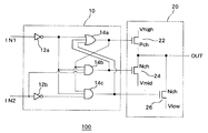
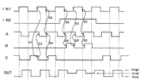
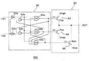
| JP2007124084A (ja) | 3値パルス発生回路 | |
| JP5219958B2 (ja) | スタートパルス生成回路 | |
| KR20230020831A (ko) | 게이트 드라이버 회로 및 그의 구동방법 | |
| JP2000221926A (ja) | ラッチ回路およびこれを搭載した液晶表示装置 | |
| JPH06350933A (ja) | シフトレジスタ | |
| JP2006279883A (ja) | ドライバ回路 | |
| TWI915575B (zh) | 閘極驅動器電路和用於驅動閘極驅動器電路的方法 | |
| JP5975322B2 (ja) | 固体撮像素子の駆動装置 | |
| JP2008092343A (ja) | アナログ信号伝達回路 | |
| JP2006098764A (ja) | 表示装置の駆動回路 | |
| JP2008165169A (ja) | 電圧駆動回路 | |
| JPH10243293A (ja) | 固体撮像装置 | |
| JP2005051616A (ja) | 固体撮像装置 |
Legal Events
| Date | Code | Title | Description |
|---|---|---|---|
| A521 | Request for written amendment filed |
Free format text: JAPANESE INTERMEDIATE CODE: A523 Effective date: 20080416 |
|
| A621 | Written request for application examination |
Free format text: JAPANESE INTERMEDIATE CODE: A621 Effective date: 20081003 |
|
| A977 | Report on retrieval |
Free format text: JAPANESE INTERMEDIATE CODE: A971007 Effective date: 20110127 |
|
| A131 | Notification of reasons for refusal |
Free format text: JAPANESE INTERMEDIATE CODE: A131 Effective date: 20110201 |
|
| A02 | Decision of refusal |
Free format text: JAPANESE INTERMEDIATE CODE: A02 Effective date: 20110712 |