JP2005294582A - 半導体装置の製造方法 - Google Patents
半導体装置の製造方法 Download PDFInfo
- Publication number
- JP2005294582A JP2005294582A JP2004108442A JP2004108442A JP2005294582A JP 2005294582 A JP2005294582 A JP 2005294582A JP 2004108442 A JP2004108442 A JP 2004108442A JP 2004108442 A JP2004108442 A JP 2004108442A JP 2005294582 A JP2005294582 A JP 2005294582A
- Authority
- JP
- Japan
- Prior art keywords
- plug
- semiconductor device
- forming
- film
- hole
- Prior art date
- Legal status (The legal status is an assumption and is not a legal conclusion. Google has not performed a legal analysis and makes no representation as to the accuracy of the status listed.)
- Granted
Links
Images


Classifications
-
- H—ELECTRICITY
- H10—SEMICONDUCTOR DEVICES; ELECTRIC SOLID-STATE DEVICES NOT OTHERWISE PROVIDED FOR
- H10W—GENERIC PACKAGES, INTERCONNECTIONS, CONNECTORS OR OTHER CONSTRUCTIONAL DETAILS OF DEVICES COVERED BY CLASS H10
- H10W20/00—Interconnections in chips, wafers or substrates
- H10W20/01—Manufacture or treatment
- H10W20/021—Manufacture or treatment of interconnections within wafers or substrates
- H10W20/023—Manufacture or treatment of interconnections within wafers or substrates the interconnections being through-semiconductor vias
- H10W20/0234—Manufacture or treatment of interconnections within wafers or substrates the interconnections being through-semiconductor vias comprising etching via holes that stop on pads or on electrodes
-
- H—ELECTRICITY
- H10—SEMICONDUCTOR DEVICES; ELECTRIC SOLID-STATE DEVICES NOT OTHERWISE PROVIDED FOR
- H10W—GENERIC PACKAGES, INTERCONNECTIONS, CONNECTORS OR OTHER CONSTRUCTIONAL DETAILS OF DEVICES COVERED BY CLASS H10
- H10W20/00—Interconnections in chips, wafers or substrates
- H10W20/01—Manufacture or treatment
- H10W20/021—Manufacture or treatment of interconnections within wafers or substrates
- H10W20/023—Manufacture or treatment of interconnections within wafers or substrates the interconnections being through-semiconductor vias
- H10W20/0242—Manufacture or treatment of interconnections within wafers or substrates the interconnections being through-semiconductor vias comprising etching via holes from the back sides of the chips, wafers or substrates
-
- H—ELECTRICITY
- H10—SEMICONDUCTOR DEVICES; ELECTRIC SOLID-STATE DEVICES NOT OTHERWISE PROVIDED FOR
- H10W—GENERIC PACKAGES, INTERCONNECTIONS, CONNECTORS OR OTHER CONSTRUCTIONAL DETAILS OF DEVICES COVERED BY CLASS H10
- H10W20/00—Interconnections in chips, wafers or substrates
- H10W20/01—Manufacture or treatment
- H10W20/021—Manufacture or treatment of interconnections within wafers or substrates
- H10W20/023—Manufacture or treatment of interconnections within wafers or substrates the interconnections being through-semiconductor vias
- H10W20/0245—Manufacture or treatment of interconnections within wafers or substrates the interconnections being through-semiconductor vias comprising use of blind vias during the manufacture
-
- H—ELECTRICITY
- H10—SEMICONDUCTOR DEVICES; ELECTRIC SOLID-STATE DEVICES NOT OTHERWISE PROVIDED FOR
- H10W—GENERIC PACKAGES, INTERCONNECTIONS, CONNECTORS OR OTHER CONSTRUCTIONAL DETAILS OF DEVICES COVERED BY CLASS H10
- H10W20/00—Interconnections in chips, wafers or substrates
- H10W20/20—Interconnections within wafers or substrates, e.g. through-silicon vias [TSV]
- H10W20/211—Through-semiconductor vias, e.g. TSVs
- H10W20/212—Top-view shapes or dispositions, e.g. top-view layouts of the vias
- H10W20/2125—Top-view shapes
-
- H—ELECTRICITY
- H10—SEMICONDUCTOR DEVICES; ELECTRIC SOLID-STATE DEVICES NOT OTHERWISE PROVIDED FOR
- H10W—GENERIC PACKAGES, INTERCONNECTIONS, CONNECTORS OR OTHER CONSTRUCTIONAL DETAILS OF DEVICES COVERED BY CLASS H10
- H10W20/00—Interconnections in chips, wafers or substrates
- H10W20/20—Interconnections within wafers or substrates, e.g. through-silicon vias [TSV]
- H10W20/211—Through-semiconductor vias, e.g. TSVs
- H10W20/213—Cross-sectional shapes or dispositions
- H10W20/2134—TSVs extending from the semiconductor wafer into back-end-of-line layers
-
- H—ELECTRICITY
- H10—SEMICONDUCTOR DEVICES; ELECTRIC SOLID-STATE DEVICES NOT OTHERWISE PROVIDED FOR
- H10W—GENERIC PACKAGES, INTERCONNECTIONS, CONNECTORS OR OTHER CONSTRUCTIONAL DETAILS OF DEVICES COVERED BY CLASS H10
- H10W72/00—Interconnections or connectors in packages
- H10W72/01—Manufacture or treatment
- H10W72/012—Manufacture or treatment of bump connectors, dummy bumps or thermal bumps
-
- H—ELECTRICITY
- H10—SEMICONDUCTOR DEVICES; ELECTRIC SOLID-STATE DEVICES NOT OTHERWISE PROVIDED FOR
- H10W—GENERIC PACKAGES, INTERCONNECTIONS, CONNECTORS OR OTHER CONSTRUCTIONAL DETAILS OF DEVICES COVERED BY CLASS H10
- H10W72/00—Interconnections or connectors in packages
- H10W72/071—Connecting or disconnecting
- H10W72/072—Connecting or disconnecting of bump connectors
- H10W72/07251—Connecting or disconnecting of bump connectors characterised by changes in properties of the bump connectors during connecting
-
- H—ELECTRICITY
- H10—SEMICONDUCTOR DEVICES; ELECTRIC SOLID-STATE DEVICES NOT OTHERWISE PROVIDED FOR
- H10W—GENERIC PACKAGES, INTERCONNECTIONS, CONNECTORS OR OTHER CONSTRUCTIONAL DETAILS OF DEVICES COVERED BY CLASS H10
- H10W72/00—Interconnections or connectors in packages
- H10W72/20—Bump connectors, e.g. solder bumps or copper pillars; Dummy bumps; Thermal bumps
- H10W72/221—Structures or relative sizes
-
- H—ELECTRICITY
- H10—SEMICONDUCTOR DEVICES; ELECTRIC SOLID-STATE DEVICES NOT OTHERWISE PROVIDED FOR
- H10W—GENERIC PACKAGES, INTERCONNECTIONS, CONNECTORS OR OTHER CONSTRUCTIONAL DETAILS OF DEVICES COVERED BY CLASS H10
- H10W72/00—Interconnections or connectors in packages
- H10W72/20—Bump connectors, e.g. solder bumps or copper pillars; Dummy bumps; Thermal bumps
- H10W72/241—Dispositions, e.g. layouts
- H10W72/244—Dispositions, e.g. layouts relative to underlying supporting features, e.g. bond pads, RDLs or vias
-
- H—ELECTRICITY
- H10—SEMICONDUCTOR DEVICES; ELECTRIC SOLID-STATE DEVICES NOT OTHERWISE PROVIDED FOR
- H10W—GENERIC PACKAGES, INTERCONNECTIONS, CONNECTORS OR OTHER CONSTRUCTIONAL DETAILS OF DEVICES COVERED BY CLASS H10
- H10W72/00—Interconnections or connectors in packages
- H10W72/20—Bump connectors, e.g. solder bumps or copper pillars; Dummy bumps; Thermal bumps
- H10W72/241—Dispositions, e.g. layouts
- H10W72/247—Dispositions of multiple bumps
- H10W72/248—Top-view layouts, e.g. mirror arrays
-
- H—ELECTRICITY
- H10—SEMICONDUCTOR DEVICES; ELECTRIC SOLID-STATE DEVICES NOT OTHERWISE PROVIDED FOR
- H10W—GENERIC PACKAGES, INTERCONNECTIONS, CONNECTORS OR OTHER CONSTRUCTIONAL DETAILS OF DEVICES COVERED BY CLASS H10
- H10W72/00—Interconnections or connectors in packages
- H10W72/20—Bump connectors, e.g. solder bumps or copper pillars; Dummy bumps; Thermal bumps
- H10W72/251—Materials
- H10W72/252—Materials comprising solid metals or solid metalloids, e.g. PbSn, Ag or Cu
-
- H—ELECTRICITY
- H10—SEMICONDUCTOR DEVICES; ELECTRIC SOLID-STATE DEVICES NOT OTHERWISE PROVIDED FOR
- H10W—GENERIC PACKAGES, INTERCONNECTIONS, CONNECTORS OR OTHER CONSTRUCTIONAL DETAILS OF DEVICES COVERED BY CLASS H10
- H10W72/00—Interconnections or connectors in packages
- H10W72/20—Bump connectors, e.g. solder bumps or copper pillars; Dummy bumps; Thermal bumps
- H10W72/29—Bond pads specially adapted therefor
-
- H—ELECTRICITY
- H10—SEMICONDUCTOR DEVICES; ELECTRIC SOLID-STATE DEVICES NOT OTHERWISE PROVIDED FOR
- H10W—GENERIC PACKAGES, INTERCONNECTIONS, CONNECTORS OR OTHER CONSTRUCTIONAL DETAILS OF DEVICES COVERED BY CLASS H10
- H10W72/00—Interconnections or connectors in packages
- H10W72/90—Bond pads, in general
- H10W72/921—Structures or relative sizes of bond pads
- H10W72/923—Bond pads having multiple stacked layers
- H10W72/9232—Bond pads having multiple stacked layers with additional elements interposed between layers
-
- H—ELECTRICITY
- H10—SEMICONDUCTOR DEVICES; ELECTRIC SOLID-STATE DEVICES NOT OTHERWISE PROVIDED FOR
- H10W—GENERIC PACKAGES, INTERCONNECTIONS, CONNECTORS OR OTHER CONSTRUCTIONAL DETAILS OF DEVICES COVERED BY CLASS H10
- H10W72/00—Interconnections or connectors in packages
- H10W72/90—Bond pads, in general
- H10W72/931—Shapes of bond pads
- H10W72/934—Cross-sectional shape, i.e. in side view
-
- H—ELECTRICITY
- H10—SEMICONDUCTOR DEVICES; ELECTRIC SOLID-STATE DEVICES NOT OTHERWISE PROVIDED FOR
- H10W—GENERIC PACKAGES, INTERCONNECTIONS, CONNECTORS OR OTHER CONSTRUCTIONAL DETAILS OF DEVICES COVERED BY CLASS H10
- H10W72/00—Interconnections or connectors in packages
- H10W72/90—Bond pads, in general
- H10W72/941—Dispositions of bond pads
- H10W72/9415—Dispositions of bond pads relative to the surface, e.g. recessed, protruding
-
- H—ELECTRICITY
- H10—SEMICONDUCTOR DEVICES; ELECTRIC SOLID-STATE DEVICES NOT OTHERWISE PROVIDED FOR
- H10W—GENERIC PACKAGES, INTERCONNECTIONS, CONNECTORS OR OTHER CONSTRUCTIONAL DETAILS OF DEVICES COVERED BY CLASS H10
- H10W72/00—Interconnections or connectors in packages
- H10W72/90—Bond pads, in general
- H10W72/941—Dispositions of bond pads
- H10W72/942—Dispositions of bond pads relative to underlying supporting features, e.g. bond pads, RDLs or vias
-
- H—ELECTRICITY
- H10—SEMICONDUCTOR DEVICES; ELECTRIC SOLID-STATE DEVICES NOT OTHERWISE PROVIDED FOR
- H10W—GENERIC PACKAGES, INTERCONNECTIONS, CONNECTORS OR OTHER CONSTRUCTIONAL DETAILS OF DEVICES COVERED BY CLASS H10
- H10W72/00—Interconnections or connectors in packages
- H10W72/90—Bond pads, in general
- H10W72/951—Materials of bond pads
- H10W72/952—Materials of bond pads comprising metals or metalloids, e.g. PbSn, Ag or Cu
Landscapes
- Internal Circuitry In Semiconductor Integrated Circuit Devices (AREA)
Abstract
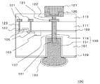
【解決手段】 半導体装置100に導電性の小径プラグ119と導電性の大径プラグ131とからなる貫通電極135を設ける。小径プラグ119の断面積を、それぞれ接続プラグ123の断面積および径よりも大きく大径プラグ131の断面積および径よりも小さくする。また、シリコン基板101から小径プラグ119が突出した突出部141を大径プラグ131の上面に貫入させる。また、小径プラグ119の上面を第一配線121と接続させる。
【選択図】 図1
Description
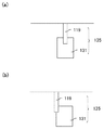
図1は、本実施形態に係る半導体装置の構成を模式的に示す断面図である。図1の半導体装置100は、シリコン基板101、エッチングストッパ膜109、最下層絶縁膜111、第一配線層絶縁膜113の積層構造を有し、シリコン基板101、エッチングストッパ膜109、および最下層絶縁膜111を貫通する貫通電極135が設けられている。
まず、半導体装置100においては、貫通電極135が小径プラグ119および大径プラグ131の二つのプラグからなる。小径プラグ119の端部の突出部141は、大径プラグ131に内包されている。
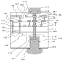
第一の実施形態に記載の半導体装置100を以下のようにして作製することもできる。以下、図2(a)〜図2(d)を参照しつつ、第一の実施形態と異なる点を中心に説明する。
第一の実施形態に記載の半導体装置100を以下のようにして作製することもできる。以下、以下、図2(a)〜図2(d)を参照しつつ、第一または第二の実施形態と異なる点を中心に説明する。
101 シリコン基板
102 半導体装置
103 素子分離膜
104 半導体装置
105 拡散層
107 ゲート電極
109 エッチングストッパ膜
112 配線用絶縁膜
113 第一配線層絶縁膜
114 プラグ用絶縁膜
115 粘着剤層
117 支持体
119 小径プラグ
121 第一配線
122 接続プラグ
123 接続プラグ
125 パッド
127 バンプ
129 電着絶縁膜
131 大径プラグ
133 めっき膜
135 貫通電極
137 SiN膜
139 開口部
141 突出部
153 配線
154 配線
161 絶縁層
163 絶縁層
165 配線
167 接続プラグ
169 配線
171 接続プラグ
Claims (9)
- 半導体基板の素子形成面の側に第一の孔を形成する工程と、
前記第一の孔の内壁に、絶縁材料からなるバリア膜を形成する工程と、
前記第一の孔の内部を埋め込むように第一の金属膜を埋設する工程と、
前記第一の孔の外部に形成された前記第一の金属膜を除去し、前記第一の孔の内部に第一のプラグを形成する工程と、
裏面の側から前記半導体基板を選択的に除去して第二の孔を形成し、前記第二の孔の内部に前記第一のプラグの一部を露出させる工程と、
前記第二の孔の内面の前記第一のプラグを除く領域に選択的に絶縁材料を付着させる工程と、
絶縁材料を付着させる前記工程の後、露出した前記バリア膜の少なくとも一部を除去し、前記第一の金属膜を露出させる工程と、
前記第二の孔の内部を埋めるように選択的に第二の金属膜を成長させて、前記第一のプラグの一部を内包する第二のプラグを形成する工程と、
を含むことを特徴とする半導体装置の製造方法。 - 請求項1に記載の半導体装置の製造方法において、第二のプラグを形成する前記工程は、露出した前記第一の金属膜を起点として前記第二の孔の内部を埋めるように前記第二の金属膜を成長させる工程を含むことを特徴とする半導体装置の製造方法。
- 請求項1または2に記載の半導体装置の製造方法において、前記絶縁材料は電着材料であることを特徴とする半導体装置の製造方法。
- 請求項3に記載の半導体装置の製造方法において、前記電着材料は電着ポリイミドであることを特徴とする半導体装置の製造方法。
- 請求項1乃至4いずれかに記載の半導体装置の製造方法において、前記第二の孔は前記第一の孔よりも断面積が大きいことを特徴とする半導体装置の製造方法。
- 請求項1乃至5いずれかに記載の半導体装置の製造方法において、第二のプラグを形成する前記工程の前に、前記第二の孔の前記内面に金属のシード層を形成する工程を含み、
第二のプラグを形成する前記工程は、前記シード層を起点として前記第二の金属膜を成長させる工程を含むことを特徴とする半導体装置の製造方法。 - 請求項1乃至6いずれかに記載の半導体装置の製造方法において、第二の孔を形成する前記工程の後、絶縁材料を付着させる前記工程の前に、前記第二の孔の前記内面の前記第一のプラグを除く前記領域に選択的に金属のシード層を形成する工程を含み、
絶縁材料を付着させる前記工程は、前記シード層に前記絶縁材料を付着させる工程を含むことを特徴とする半導体装置の製造方法。 - 請求項1乃至7いずれかに記載の半導体装置の製造方法において、第一の孔を形成する前記工程は、前記半導体基板の前記素子形成面の側に絶縁膜を形成した後、前記第一の孔を形成する領域の前記絶縁膜を選択的に除去する工程を含むことを特徴とする半導体装置の製造方法。
- 請求項8に記載の半導体装置の製造方法において、
第一のプラグを形成する前記工程の後に、前記半導体基板の前記絶縁膜上に配線層を形成する工程を含み、
配線層を形成する前記工程は、前記第一のプラグに接続する配線を形成する工程を含むことを特徴とする半導体装置の製造方法。
Priority Applications (3)
| Application Number | Priority Date | Filing Date | Title |
|---|---|---|---|
| JP2004108442A JP4327644B2 (ja) | 2004-03-31 | 2004-03-31 | 半導体装置の製造方法 |
| US11/085,135 US7528068B2 (en) | 2004-03-31 | 2005-03-22 | Method for manufacturing semiconductor device |
| TW094110022A TWI293473B (en) | 2004-03-31 | 2005-03-30 | Method for manufacturing semiconductor device |
Applications Claiming Priority (1)
| Application Number | Priority Date | Filing Date | Title |
|---|---|---|---|
| JP2004108442A JP4327644B2 (ja) | 2004-03-31 | 2004-03-31 | 半導体装置の製造方法 |
Publications (2)
| Publication Number | Publication Date |
|---|---|
| JP2005294582A true JP2005294582A (ja) | 2005-10-20 |
| JP4327644B2 JP4327644B2 (ja) | 2009-09-09 |
Family
ID=35096828
Family Applications (1)
| Application Number | Title | Priority Date | Filing Date |
|---|---|---|---|
| JP2004108442A Expired - Fee Related JP4327644B2 (ja) | 2004-03-31 | 2004-03-31 | 半導体装置の製造方法 |
Country Status (3)
| Country | Link |
|---|---|
| US (1) | US7528068B2 (ja) |
| JP (1) | JP4327644B2 (ja) |
| TW (1) | TWI293473B (ja) |
Cited By (16)
| Publication number | Priority date | Publication date | Assignee | Title |
|---|---|---|---|---|
| JP2010192481A (ja) * | 2009-02-16 | 2010-09-02 | Panasonic Corp | 半導体基板と半導体パッケージおよび半導体基板の製造方法 |
| JP2010232400A (ja) * | 2009-03-27 | 2010-10-14 | Panasonic Corp | 半導体基板と半導体基板の製造方法および半導体パッケージ |
| JP2010245263A (ja) * | 2009-04-06 | 2010-10-28 | Shinko Electric Ind Co Ltd | 半導体装置及びその製造方法 |
| US7843068B2 (en) | 2005-06-30 | 2010-11-30 | Shinko Electric Industries Co., Ltd. | Semiconductor chip and method of manufacturing the same |
| JP2010278181A (ja) * | 2009-05-28 | 2010-12-09 | Shinko Electric Ind Co Ltd | 半導体装置及びその製造方法 |
| US7875552B2 (en) | 2008-06-10 | 2011-01-25 | Samsung Electronics Co., Ltd. | Methods of forming integrated circuit chips having vertically extended through-substrate vias therein and chips formed thereby |
| US8034704B2 (en) | 2006-12-06 | 2011-10-11 | Sony Corporation | Method for manufacturing semiconductor device and semiconductor device |
| US8102049B2 (en) | 2006-08-25 | 2012-01-24 | Renesas Electronics Corporation | Semiconductor device including through electrode and method of manufacturing the same |
| US8217516B2 (en) | 2008-06-06 | 2012-07-10 | Renesas Electronics Corporation | Semiconductor device and method of manufacturing the same |
| US8252628B2 (en) | 2007-03-15 | 2012-08-28 | Sony Corporation | Semiconductor device and method of manufacturing the same |
| JP2012164792A (ja) * | 2011-02-07 | 2012-08-30 | Nippon Telegr & Teleph Corp <Ntt> | ヴィア構造およびその作製方法 |
| JP2014049500A (ja) * | 2012-08-29 | 2014-03-17 | Renesas Electronics Corp | 半導体装置及びその製造方法 |
| WO2014061643A1 (ja) * | 2012-10-16 | 2014-04-24 | 東京エレクトロン株式会社 | 半導体装置の製造方法及び半導体装置 |
| JP2014517534A (ja) * | 2011-06-06 | 2014-07-17 | マイクロン テクノロジー, インク. | 基板貫通相互接続を有する半導体構成と、基板貫通相互接続を形成する方法 |
| JP2016181716A (ja) * | 2016-06-15 | 2016-10-13 | ルネサスエレクトロニクス株式会社 | 半導体装置及びその製造方法 |
| CN110718504A (zh) * | 2019-09-02 | 2020-01-21 | 长江存储科技有限责任公司 | 插塞结构、三维存储器的形成方法和三维存储器 |
Families Citing this family (26)
| Publication number | Priority date | Publication date | Assignee | Title |
|---|---|---|---|---|
| JP4265668B2 (ja) * | 2007-03-08 | 2009-05-20 | ソニー株式会社 | 回路基板の製造方法および回路基板 |
| JP2009147218A (ja) * | 2007-12-17 | 2009-07-02 | Toshiba Corp | 半導体装置とその製造方法 |
| US7803714B2 (en) * | 2008-03-31 | 2010-09-28 | Freescale Semiconductor, Inc. | Semiconductor through silicon vias of variable size and method of formation |
| WO2010035379A1 (ja) * | 2008-09-26 | 2010-04-01 | パナソニック株式会社 | 半導体装置及びその製造方法 |
| US8178953B2 (en) | 2008-09-30 | 2012-05-15 | Infineon Technologies Ag | On-chip RF shields with front side redistribution lines |
| US8169059B2 (en) * | 2008-09-30 | 2012-05-01 | Infineon Technologies Ag | On-chip RF shields with through substrate conductors |
| US8063469B2 (en) * | 2008-09-30 | 2011-11-22 | Infineon Technologies Ag | On-chip radio frequency shield with interconnect metallization |
| US8889548B2 (en) | 2008-09-30 | 2014-11-18 | Infineon Technologies Ag | On-chip RF shields with backside redistribution lines |
| US7948064B2 (en) * | 2008-09-30 | 2011-05-24 | Infineon Technologies Ag | System on a chip with on-chip RF shield |
| JP5537016B2 (ja) * | 2008-10-27 | 2014-07-02 | 株式会社東芝 | 半導体装置および半導体装置の製造方法 |
| US8227889B2 (en) * | 2008-12-08 | 2012-07-24 | United Microelectronics Corp. | Semiconductor device |
| US8513119B2 (en) | 2008-12-10 | 2013-08-20 | Taiwan Semiconductor Manufacturing Company, Ltd. | Method of forming bump structure having tapered sidewalls for stacked dies |
| US7786008B2 (en) * | 2008-12-12 | 2010-08-31 | Stats Chippac Ltd. | Integrated circuit packaging system having through silicon vias with partial depth metal fill regions and method of manufacture thereof |
| US20100171197A1 (en) * | 2009-01-05 | 2010-07-08 | Hung-Pin Chang | Isolation Structure for Stacked Dies |
| US8791549B2 (en) * | 2009-09-22 | 2014-07-29 | Taiwan Semiconductor Manufacturing Company, Ltd. | Wafer backside interconnect structure connected to TSVs |
| US8466059B2 (en) | 2010-03-30 | 2013-06-18 | Taiwan Semiconductor Manufacturing Company, Ltd. | Multi-layer interconnect structure for stacked dies |
| TWI441292B (zh) * | 2011-03-02 | 2014-06-11 | 矽品精密工業股份有限公司 | 半導體結構及其製法 |
| US8853857B2 (en) * | 2011-05-05 | 2014-10-07 | International Business Machines Corporation | 3-D integration using multi stage vias |
| JP2012256679A (ja) | 2011-06-08 | 2012-12-27 | Elpida Memory Inc | 半導体装置及びその製造方法 |
| US8900994B2 (en) | 2011-06-09 | 2014-12-02 | Taiwan Semiconductor Manufacturing Company, Ltd. | Method for producing a protective structure |
| US20130015504A1 (en) * | 2011-07-11 | 2013-01-17 | Chien-Li Kuo | Tsv structure and method for forming the same |
| DE102011081100A1 (de) * | 2011-08-17 | 2013-02-21 | Siemens Aktiengesellschaft | Anordnung mit Photozellen |
| US9159699B2 (en) * | 2012-11-13 | 2015-10-13 | Delta Electronics, Inc. | Interconnection structure having a via structure |
| JP6502751B2 (ja) * | 2015-05-29 | 2019-04-17 | 東芝メモリ株式会社 | 半導体装置および半導体装置の製造方法 |
| KR102542614B1 (ko) | 2017-10-30 | 2023-06-15 | 삼성전자주식회사 | 이미지 센서 |
| US11843020B2 (en) | 2017-10-30 | 2023-12-12 | Samsung Electronics Co., Ltd. | Image sensor |
Family Cites Families (11)
| Publication number | Priority date | Publication date | Assignee | Title |
|---|---|---|---|---|
| US3911475A (en) * | 1972-04-19 | 1975-10-07 | Westinghouse Electric Corp | Encapsulated solid state electronic devices having a sealed lead-encapsulant interface |
| US6690044B1 (en) * | 1993-03-19 | 2004-02-10 | Micron Technology, Inc. | Approach to avoid buckling BPSG by using an intermediate barrier layer |
| JPH10214896A (ja) * | 1996-11-29 | 1998-08-11 | Toshiba Corp | 半導体装置の製造方法及び製造装置 |
| US5990562A (en) * | 1997-02-25 | 1999-11-23 | International Business Machines Corporation | Semiconductor devices having backside probing capability |
| US6066539A (en) * | 1997-04-11 | 2000-05-23 | Micron Technology, Inc. | Honeycomb capacitor and method of fabrication |
| TW408443B (en) * | 1998-06-08 | 2000-10-11 | United Microelectronics Corp | The manufacture method of dual damascene |
| TW442873B (en) * | 1999-01-14 | 2001-06-23 | United Microelectronics Corp | Three-dimension stack-type chip structure and its manufacturing method |
| JP2000311982A (ja) | 1999-04-26 | 2000-11-07 | Toshiba Corp | 半導体装置と半導体モジュールおよびそれらの製造方法 |
| JP2001127151A (ja) * | 1999-10-26 | 2001-05-11 | Fujitsu Ltd | 半導体装置およびその製造方法 |
| US7030010B2 (en) * | 2002-08-29 | 2006-04-18 | Micron Technology, Inc. | Methods for creating electrophoretically insulated vias in semiconductive substrates and resulting structures |
| JP2004363573A (ja) * | 2003-05-15 | 2004-12-24 | Kumamoto Technology & Industry Foundation | 半導体チップ実装体およびその製造方法 |
-
2004
- 2004-03-31 JP JP2004108442A patent/JP4327644B2/ja not_active Expired - Fee Related
-
2005
- 2005-03-22 US US11/085,135 patent/US7528068B2/en not_active Expired - Fee Related
- 2005-03-30 TW TW094110022A patent/TWI293473B/zh not_active IP Right Cessation
Cited By (29)
| Publication number | Priority date | Publication date | Assignee | Title |
|---|---|---|---|---|
| US8338289B2 (en) | 2005-06-30 | 2012-12-25 | Shinko Electric Industries Co., Ltd. | Method of manufacturing a semiconductor chip including a semiconductor substrate and a through via provided in a through hole |
| US7843068B2 (en) | 2005-06-30 | 2010-11-30 | Shinko Electric Industries Co., Ltd. | Semiconductor chip and method of manufacturing the same |
| US8102049B2 (en) | 2006-08-25 | 2012-01-24 | Renesas Electronics Corporation | Semiconductor device including through electrode and method of manufacturing the same |
| US8034704B2 (en) | 2006-12-06 | 2011-10-11 | Sony Corporation | Method for manufacturing semiconductor device and semiconductor device |
| KR101455386B1 (ko) * | 2006-12-06 | 2014-10-27 | 소니 주식회사 | 반도체 장치의 제조 방법 및 반도체 장치 |
| US9379155B2 (en) | 2007-03-15 | 2016-06-28 | Sony Corporation | Semiconductor device and method of manufacturing the same |
| US11676977B2 (en) | 2007-03-15 | 2023-06-13 | Sony Group Corporation | Semiconductor device |
| US8252628B2 (en) | 2007-03-15 | 2012-08-28 | Sony Corporation | Semiconductor device and method of manufacturing the same |
| US9041179B2 (en) | 2007-03-15 | 2015-05-26 | Sony Corporation | Semiconductor device and method of manufacturing the same |
| US8791567B2 (en) | 2008-06-06 | 2014-07-29 | Renesas Electronics Corporation | Semiconductor device |
| US8217516B2 (en) | 2008-06-06 | 2012-07-10 | Renesas Electronics Corporation | Semiconductor device and method of manufacturing the same |
| US7875552B2 (en) | 2008-06-10 | 2011-01-25 | Samsung Electronics Co., Ltd. | Methods of forming integrated circuit chips having vertically extended through-substrate vias therein and chips formed thereby |
| US9219035B2 (en) | 2008-06-10 | 2015-12-22 | Samsung Electronics Co., Ltd. | Integrated circuit chips having vertically extended through-substrate vias therein |
| US8629059B2 (en) | 2008-06-10 | 2014-01-14 | Samsung Electronics Co., Ltd. | Methods of forming integrated circuit chips having vertically extended through-substrate vias therein |
| JP2010192481A (ja) * | 2009-02-16 | 2010-09-02 | Panasonic Corp | 半導体基板と半導体パッケージおよび半導体基板の製造方法 |
| JP2010232400A (ja) * | 2009-03-27 | 2010-10-14 | Panasonic Corp | 半導体基板と半導体基板の製造方法および半導体パッケージ |
| JP2010245263A (ja) * | 2009-04-06 | 2010-10-28 | Shinko Electric Ind Co Ltd | 半導体装置及びその製造方法 |
| JP2010278181A (ja) * | 2009-05-28 | 2010-12-09 | Shinko Electric Ind Co Ltd | 半導体装置及びその製造方法 |
| JP2012164792A (ja) * | 2011-02-07 | 2012-08-30 | Nippon Telegr & Teleph Corp <Ntt> | ヴィア構造およびその作製方法 |
| US9583419B2 (en) | 2011-06-06 | 2017-02-28 | Micron Technology, Inc. | Semiconductor constructions having through-substrate interconnects |
| JP2014517534A (ja) * | 2011-06-06 | 2014-07-17 | マイクロン テクノロジー, インク. | 基板貫通相互接続を有する半導体構成と、基板貫通相互接続を形成する方法 |
| US10121738B2 (en) | 2011-06-06 | 2018-11-06 | Micron Technology, Inc. | Semiconductor constructions |
| JP2014049500A (ja) * | 2012-08-29 | 2014-03-17 | Renesas Electronics Corp | 半導体装置及びその製造方法 |
| US9779992B2 (en) | 2012-08-29 | 2017-10-03 | Renesas Electronics Corporation | Semiconductor device and method of manufacturing the same |
| US9275935B2 (en) | 2012-08-29 | 2016-03-01 | Renesas Electronics Corporation | Semiconductor device and method of manufacturing the same |
| WO2014061643A1 (ja) * | 2012-10-16 | 2014-04-24 | 東京エレクトロン株式会社 | 半導体装置の製造方法及び半導体装置 |
| JP2016181716A (ja) * | 2016-06-15 | 2016-10-13 | ルネサスエレクトロニクス株式会社 | 半導体装置及びその製造方法 |
| CN110718504A (zh) * | 2019-09-02 | 2020-01-21 | 长江存储科技有限责任公司 | 插塞结构、三维存储器的形成方法和三维存储器 |
| CN110718504B (zh) * | 2019-09-02 | 2022-07-29 | 长江存储科技有限责任公司 | 插塞结构、三维存储器的形成方法和三维存储器 |
Also Published As
| Publication number | Publication date |
|---|---|
| JP4327644B2 (ja) | 2009-09-09 |
| TWI293473B (en) | 2008-02-11 |
| TW200535978A (en) | 2005-11-01 |
| US20050233581A1 (en) | 2005-10-20 |
| US7528068B2 (en) | 2009-05-05 |
Similar Documents
| Publication | Publication Date | Title |
|---|---|---|
| JP4327644B2 (ja) | 半導体装置の製造方法 | |
| JP4439976B2 (ja) | 半導体装置およびその製造方法 | |
| JP4800585B2 (ja) | 貫通電極の製造方法、シリコンスペーサーの製造方法 | |
| US8183685B2 (en) | Semiconductor device | |
| JP5021992B2 (ja) | 半導体装置およびその製造方法 | |
| JP2006019455A (ja) | 半導体装置およびその製造方法 | |
| JP2011258687A (ja) | 半導体装置およびその製造方法 | |
| CN114078954B (zh) | 存储器结构及其形成方法 | |
| JP2010080750A (ja) | 半導体装置及びその製造方法 | |
| CN108630647B (zh) | 半导体装置及其制造方法 | |
| CN108666284A (zh) | 半导体装置的制造方法及半导体装置 | |
| TWI344685B (en) | An integrated circuit device and a process for forming the same | |
| CN102760710B (zh) | 硅穿孔结构及其形成方法 | |
| KR20010062445A (ko) | 반도체 장치 및 본드 패드 형성 프로세스 | |
| KR101139650B1 (ko) | 배선 기판, 그 제조 방법, 및 반도체 장치 | |
| TWI437689B (zh) | 半導體裝置 | |
| JP5834563B2 (ja) | 半導体装置の製造方法 | |
| US20060267190A1 (en) | Semiconductor device, laminated semiconductor device, and method for producing semiconductor device | |
| CN112997304A (zh) | 半导体装置 | |
| JP2009049336A (ja) | 半導体装置およびその製造方法 |
Legal Events
| Date | Code | Title | Description |
|---|---|---|---|
| A621 | Written request for application examination |
Free format text: JAPANESE INTERMEDIATE CODE: A621 Effective date: 20070208 |
|
| A977 | Report on retrieval |
Free format text: JAPANESE INTERMEDIATE CODE: A971007 Effective date: 20090430 |
|
| TRDD | Decision of grant or rejection written | ||
| A01 | Written decision to grant a patent or to grant a registration (utility model) |
Free format text: JAPANESE INTERMEDIATE CODE: A01 Effective date: 20090512 |
|
| A01 | Written decision to grant a patent or to grant a registration (utility model) |
Free format text: JAPANESE INTERMEDIATE CODE: A01 |
|
| A61 | First payment of annual fees (during grant procedure) |
Free format text: JAPANESE INTERMEDIATE CODE: A61 Effective date: 20090611 |
|
| FPAY | Renewal fee payment (event date is renewal date of database) |
Free format text: PAYMENT UNTIL: 20120619 Year of fee payment: 3 |
|
| R150 | Certificate of patent or registration of utility model |
Ref document number: 4327644 Country of ref document: JP Free format text: JAPANESE INTERMEDIATE CODE: R150 Free format text: JAPANESE INTERMEDIATE CODE: R150 |
|
| FPAY | Renewal fee payment (event date is renewal date of database) |
Free format text: PAYMENT UNTIL: 20120619 Year of fee payment: 3 |
|
| S533 | Written request for registration of change of name |
Free format text: JAPANESE INTERMEDIATE CODE: R313533 |
|
| FPAY | Renewal fee payment (event date is renewal date of database) |
Free format text: PAYMENT UNTIL: 20120619 Year of fee payment: 3 |
|
| R350 | Written notification of registration of transfer |
Free format text: JAPANESE INTERMEDIATE CODE: R350 |
|
| FPAY | Renewal fee payment (event date is renewal date of database) |
Free format text: PAYMENT UNTIL: 20120619 Year of fee payment: 3 |
|
| FPAY | Renewal fee payment (event date is renewal date of database) |
Free format text: PAYMENT UNTIL: 20130619 Year of fee payment: 4 |
|
| FPAY | Renewal fee payment (event date is renewal date of database) |
Free format text: PAYMENT UNTIL: 20130619 Year of fee payment: 4 |
|
| FPAY | Renewal fee payment (event date is renewal date of database) |
Free format text: PAYMENT UNTIL: 20140619 Year of fee payment: 5 |
|
| S531 | Written request for registration of change of domicile |
Free format text: JAPANESE INTERMEDIATE CODE: R313531 |
|
| R350 | Written notification of registration of transfer |
Free format text: JAPANESE INTERMEDIATE CODE: R350 |
|
| LAPS | Cancellation because of no payment of annual fees |