EP4341730B1 - Method for fabricating a blazed grating - Google Patents
Method for fabricating a blazed grating Download PDFInfo
- Publication number
- EP4341730B1 EP4341730B1 EP22723709.6A EP22723709A EP4341730B1 EP 4341730 B1 EP4341730 B1 EP 4341730B1 EP 22723709 A EP22723709 A EP 22723709A EP 4341730 B1 EP4341730 B1 EP 4341730B1
- Authority
- EP
- European Patent Office
- Prior art keywords
- substrate
- primary
- blaze
- facet
- mask layer
- Prior art date
- Legal status (The legal status is an assumption and is not a legal conclusion. Google has not performed a legal analysis and makes no representation as to the accuracy of the status listed.)
- Active
Links
Images

Classifications
-
- G—PHYSICS
- G02—OPTICS
- G02B—OPTICAL ELEMENTS, SYSTEMS OR APPARATUS
- G02B5/00—Optical elements other than lenses
- G02B5/18—Diffraction gratings
- G02B5/1847—Manufacturing methods
-
- C—CHEMISTRY; METALLURGY
- C23—COATING METALLIC MATERIAL; COATING MATERIAL WITH METALLIC MATERIAL; CHEMICAL SURFACE TREATMENT; DIFFUSION TREATMENT OF METALLIC MATERIAL; COATING BY VACUUM EVAPORATION, BY SPUTTERING, BY ION IMPLANTATION OR BY CHEMICAL VAPOUR DEPOSITION, IN GENERAL; INHIBITING CORROSION OF METALLIC MATERIAL OR INCRUSTATION IN GENERAL
- C23C—COATING METALLIC MATERIAL; COATING MATERIAL WITH METALLIC MATERIAL; SURFACE TREATMENT OF METALLIC MATERIAL BY DIFFUSION INTO THE SURFACE, BY CHEMICAL CONVERSION OR SUBSTITUTION; COATING BY VACUUM EVAPORATION, BY SPUTTERING, BY ION IMPLANTATION OR BY CHEMICAL VAPOUR DEPOSITION, IN GENERAL
- C23C16/00—Chemical coating by decomposition of gaseous compounds, without leaving reaction products of surface material in the coating, i.e. chemical vapour deposition [CVD] processes
- C23C16/02—Pretreatment of the material to be coated
- C23C16/0227—Pretreatment of the material to be coated by cleaning or etching
- C23C16/0245—Pretreatment of the material to be coated by cleaning or etching by etching with a plasma
-
- C—CHEMISTRY; METALLURGY
- C23—COATING METALLIC MATERIAL; COATING MATERIAL WITH METALLIC MATERIAL; CHEMICAL SURFACE TREATMENT; DIFFUSION TREATMENT OF METALLIC MATERIAL; COATING BY VACUUM EVAPORATION, BY SPUTTERING, BY ION IMPLANTATION OR BY CHEMICAL VAPOUR DEPOSITION, IN GENERAL; INHIBITING CORROSION OF METALLIC MATERIAL OR INCRUSTATION IN GENERAL
- C23C—COATING METALLIC MATERIAL; COATING MATERIAL WITH METALLIC MATERIAL; SURFACE TREATMENT OF METALLIC MATERIAL BY DIFFUSION INTO THE SURFACE, BY CHEMICAL CONVERSION OR SUBSTITUTION; COATING BY VACUUM EVAPORATION, BY SPUTTERING, BY ION IMPLANTATION OR BY CHEMICAL VAPOUR DEPOSITION, IN GENERAL
- C23C16/00—Chemical coating by decomposition of gaseous compounds, without leaving reaction products of surface material in the coating, i.e. chemical vapour deposition [CVD] processes
- C23C16/04—Coating on selected surface areas, e.g. using masks
- C23C16/045—Coating cavities or hollow spaces, e.g. interior of tubes; Infiltration of porous substrates
-
- C—CHEMISTRY; METALLURGY
- C23—COATING METALLIC MATERIAL; COATING MATERIAL WITH METALLIC MATERIAL; CHEMICAL SURFACE TREATMENT; DIFFUSION TREATMENT OF METALLIC MATERIAL; COATING BY VACUUM EVAPORATION, BY SPUTTERING, BY ION IMPLANTATION OR BY CHEMICAL VAPOUR DEPOSITION, IN GENERAL; INHIBITING CORROSION OF METALLIC MATERIAL OR INCRUSTATION IN GENERAL
- C23C—COATING METALLIC MATERIAL; COATING MATERIAL WITH METALLIC MATERIAL; SURFACE TREATMENT OF METALLIC MATERIAL BY DIFFUSION INTO THE SURFACE, BY CHEMICAL CONVERSION OR SUBSTITUTION; COATING BY VACUUM EVAPORATION, BY SPUTTERING, BY ION IMPLANTATION OR BY CHEMICAL VAPOUR DEPOSITION, IN GENERAL
- C23C16/00—Chemical coating by decomposition of gaseous compounds, without leaving reaction products of surface material in the coating, i.e. chemical vapour deposition [CVD] processes
- C23C16/44—Chemical coating by decomposition of gaseous compounds, without leaving reaction products of surface material in the coating, i.e. chemical vapour deposition [CVD] processes characterised by the method of coating
- C23C16/455—Chemical coating by decomposition of gaseous compounds, without leaving reaction products of surface material in the coating, i.e. chemical vapour deposition [CVD] processes characterised by the method of coating characterised by the method used for introducing gases into reaction chamber or for modifying gas flows in reaction chamber
- C23C16/45523—Pulsed gas flow or change of composition over time
- C23C16/45525—Atomic layer deposition [ALD]
- C23C16/45555—Atomic layer deposition [ALD] applied in non-semiconductor technology
-
- C—CHEMISTRY; METALLURGY
- C23—COATING METALLIC MATERIAL; COATING MATERIAL WITH METALLIC MATERIAL; CHEMICAL SURFACE TREATMENT; DIFFUSION TREATMENT OF METALLIC MATERIAL; COATING BY VACUUM EVAPORATION, BY SPUTTERING, BY ION IMPLANTATION OR BY CHEMICAL VAPOUR DEPOSITION, IN GENERAL; INHIBITING CORROSION OF METALLIC MATERIAL OR INCRUSTATION IN GENERAL
- C23C—COATING METALLIC MATERIAL; COATING MATERIAL WITH METALLIC MATERIAL; SURFACE TREATMENT OF METALLIC MATERIAL BY DIFFUSION INTO THE SURFACE, BY CHEMICAL CONVERSION OR SUBSTITUTION; COATING BY VACUUM EVAPORATION, BY SPUTTERING, BY ION IMPLANTATION OR BY CHEMICAL VAPOUR DEPOSITION, IN GENERAL
- C23C16/00—Chemical coating by decomposition of gaseous compounds, without leaving reaction products of surface material in the coating, i.e. chemical vapour deposition [CVD] processes
- C23C16/56—After-treatment
-
- G—PHYSICS
- G02—OPTICS
- G02B—OPTICAL ELEMENTS, SYSTEMS OR APPARATUS
- G02B5/00—Optical elements other than lenses
- G02B5/18—Diffraction gratings
- G02B5/1847—Manufacturing methods
- G02B5/1857—Manufacturing methods using exposure or etching means, e.g. holography, photolithography, exposure to electron or ion beams
-
- G—PHYSICS
- G02—OPTICS
- G02B—OPTICAL ELEMENTS, SYSTEMS OR APPARATUS
- G02B5/00—Optical elements other than lenses
- G02B5/18—Diffraction gratings
- G02B5/1861—Reflection gratings characterised by their structure, e.g. step profile, contours of substrate or grooves, pitch variations, materials
-
- G—PHYSICS
- G03—PHOTOGRAPHY; CINEMATOGRAPHY; ANALOGOUS TECHNIQUES USING WAVES OTHER THAN OPTICAL WAVES; ELECTROGRAPHY; HOLOGRAPHY
- G03F—PHOTOMECHANICAL PRODUCTION OF TEXTURED OR PATTERNED SURFACES, e.g. FOR PRINTING, FOR PROCESSING OF SEMICONDUCTOR DEVICES; MATERIALS THEREFOR; ORIGINALS THEREFOR; APPARATUS SPECIALLY ADAPTED THEREFOR
- G03F7/00—Photomechanical, e.g. photolithographic, production of textured or patterned surfaces, e.g. printing surfaces; Materials therefor, e.g. comprising photoresists; Apparatus specially adapted therefor
- G03F7/0005—Production of optical devices or components in so far as characterised by the lithographic processes or materials used therefor
- G03F7/001—Phase modulating patterns, e.g. refractive index patterns
-
- G—PHYSICS
- G03—PHOTOGRAPHY; CINEMATOGRAPHY; ANALOGOUS TECHNIQUES USING WAVES OTHER THAN OPTICAL WAVES; ELECTROGRAPHY; HOLOGRAPHY
- G03H—HOLOGRAPHIC PROCESSES OR APPARATUS
- G03H1/00—Holographic processes or apparatus using light, infrared or ultraviolet waves for obtaining holograms or for obtaining an image from them; Details peculiar thereto
- G03H1/04—Processes or apparatus for producing holograms
- G03H1/18—Particular processing of hologram record carriers, e.g. for obtaining blazed holograms
- G03H1/182—Post-exposure processing, e.g. latensification
Definitions
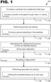
- FIG. 1 illustrates method 100 for fabricating a blazed grating comprising a ridge having a blaze facet facing a blaze facet direction and an anti-blaze facet facing an anti-blaze facet direction, the blaze facet direction and the anti-blaze facet direction extending along a grating cross-sectional plane.
- a method for fabricating a blazed grating may be identical, similar, or different to the method 100 of the embodiment of FIG. 1 .
- the method 100 comprises providing a substrate and a patterned mask layer 110 on the substrate, performing primary dry etching 120 of the substrate such that primary ions are accelerated towards a primary etch direction to impinge on the substrate, and performing secondary dry etching 150 of the substrate such that secondary ions are accelerated towards a secondary etch direction to impinge on the substrate.
- dry etching may refer to removal of material by exposure to ion bombardment.
- Typical dry etching techniques include Reactive Ion Etching (RIE), Deep Reactive Ion Etching (DRIE), Inductively Coupled Plasma Reactive Ion Etching (ICP-RIE), ion milling, Ion beam Etching (IBE), Reactive Ion Beam Etching (RIBE), and variants thereof.
- performing dry etching of a substrate such that specific ions are "accelerated towards” a specific direction to impinge on the substrate may refer to the ions being provided with an average velocity, e.g., a drift velocity, towards the specific direction.
- an average velocity e.g., a drift velocity
- such ions may be accelerated towards a specific direction by an electric field.
- a primary projection of the primary etch direction onto the grating cross-sectional plane and a secondary projection of the secondary etch direction onto the grating cross-sectional plane extend perpendicular to one and the other of the blaze facet direction and the anti-blaze facet direction, respectively, and ions (of the primary ions and the secondary ions) accelerated towards a direction with a projection onto the grating cross-sectional plane perpendicular to the blaze facet direction are collimated to form a collimated ion beam for etching the substrate.
- such primary etch direction and secondary etch direction and utilization of a collimated ion beam for etching a substrate perpendicular to a blaze facet direction may facilitate fabricating blazed gratings with sharper or less-rounded features, e.g., apexes and/or facets.
- a "collimated ion beam” may refer to a beam of ions propagating from a collimator towards a specific etch direction, e.g., a primary etch direction or a secondary etch direction.
- a collimated ion beam may be referred to as a collimated ion beam, for example, if the ion beam has a maximum angular deviation from the primary etch direction of 4°, 3°, or 2°.
- a collimated ion beam is formed for etching a substrate, such maximum angular deviation may be determined at the location of the substrate.
- the process of performing primary dry etching 120 may optionally comprise forming a groove extending in the substrate 124 along the primary etch direction
- the method 100 may optionally comprise depositing first material into the groove 130 to form an interstitial feature
- the process of performing secondary dry etching 150 may optionally comprise utilizing the interstitial feature as an etch stop 154.
- utilization of an interstitial feature as an etch stop while performing secondary dry etching may facilitate fabrication of blazed gratings with sharper, less rounded features and/or smoother and/or more even facets.
- a method for fabricating a blazed grating may or may not comprise one or more of such features.
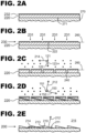
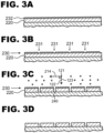
- FIGs. 2A through 2E schematically depict a series of subsequent stages of a method for fabricating a blazed grating 200, which comprises a ridge 210 having a blaze facet 211 facing a blaze facet direction 212 and an anti-blaze facet 213 facing an anti-blaze facet direction 214, the blaze facet direction 212 and the anti-blaze facet 213 extending along a grating cross-sectional plane 215, according to an embodiment.
- the grating cross-sectional plane 215 extends perpendicular to the plane of the drawings of FIGs. 2A through 2E .
- a method for fabricating a blazed grating may comprise a series of stages similar or different to the stages of the method of the embodiment of FIG. 2 .
- the blazed grating 200 comprises a plurality of ridges 210, each ridge of the plurality of ridges 210 having a blaze facet 211 facing the blaze facet direction 212 and an anti-blaze facet 213 facing the anti-blaze facet direction 214.
- a blazed grating may comprise at least one such ridge or a plurality of, i.e., at least two, such ridges.
- the method comprises providing a substrate 220 and a patterned mask layer 230 on the substrate 220.
- the process of providing the substrate 220 and the patterned mask layer 230 comprises providing a coating 232 on the substrate 220 and providing a plurality of elongated through-holes 231 in the coating 232 to form the mask layer 230.
- the plurality of elongated through-holes 231 extends perpendicular to the grating cross-sectional plane 215.
- the mask layer 230 of the embodiment of FIG. 2 may be formed of aluminum oxide (AlO 2 ) deposited by electron beam evaporation.
- a mask layer comprises inorganic material(s), including oxide and/or nitride material(s), such as aluminum oxide (AlO 2 /AlO x ), titanium oxide (TiO 2 /TiO 2 ), silicon oxide (SiO 2 /SiO x ) and/or silicon nitride (Si 2 N 3 /SiN x ), which may be formed using any suitable process(es), for example, sputtering, evaporation, Chemical Vapor Deposition (CVD), Plasma Enhanced Chemical Vapor Deposition (PECVD), Inductively Coupled Plasma Chemical Vapor Deposition (ICP-CVD), Atomic Layer Deposition (ALD), and/or variants thereof.
- CVD Chemical Vapor Deposition
- PECVD Plasma Enhanced Chemical Vapor Deposition
- ICP-CVD Inductive
- the method of the embodiment of FIG. 2 may constitute an example of a method for fabricating a blazed grating, whereby a blazed grating is formed onto a face of a waveguide for coupling light into the waveguide and/or out of the waveguide.
- the substrate 220 may be arranged onto a face 271 of a waveguide 270.
- a blazed grating may be formed for any suitable use(s) in any suitable application(s), for example, onto a face of a waveguide for coupling light into the waveguide and/or out of the waveguide.
- the blazed grating 200 of the embodiment of FIG. 2 is formed into an additional material layer arranged onto the waveguide 270.
- said blazed grating may or may not be arranged onto such additional material layer.
- a blazed grating may be formed directly into a waveguide.
- the method comprises performing primary dry etching of the substrate 220 such that primary ions 121, indicated schematically by white dots, are accelerated towards a primary etch direction 122 to impinge on the substrate 220.
- a primary projection 123 of the primary etch direction 122 onto the grating cross-sectional plane 215 extends perpendicular to anti-blaze facet direction 214.
- the process of performing primary dry etching of the embodiment of FIG. 2 comprises forming a groove 240 extending in the substrate 220 along the primary etch direction 122.
- a process of performing primary dry etching may or may not comprise forming such groove.
- a "base plane” may refer to a fictitious surface along which an interface between a substrate and a mask layer extends.
- a base plane may be planar, for example, in case of a flat interface, or curved, for example, in case of a curved interface.
- a primary projection and a secondary projection extending obliquely with respect to a base plane may enable forming blazed gratings with slanted anti-blaze facets, which may, for example, facilitate spatially modulating diffraction efficiencies of the blazed gratings.
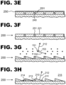
- the method comprises performing secondary dry etching of the substrate 220 such that secondary ions 151, indicated schematically by black dots, are accelerated towards a secondary etch direction 152 to impinge on the substrate 220.
- the method further comprises a post-processing step, whereby portions of the substrate 220 released during the process of performing secondary dry etching are removed to form the plurality of ridges 210.
- a method for fabricating a blazed grating may or may not comprise such post-processing step.
- the primary ions 121 may exhibit a first primary chemical reactivity with the mask layer 230 and a second primary chemical reactivity higher than the first primary chemical reactivity with the substrate 220.
- the secondary ions 151 may exhibit a first secondary chemical reactivity with the mask layer 230 and a second secondary chemical reactivity higher than the first secondary chemical reactivity with the substrate 220.
- etching a substrate may increase selectivity of dry etching processes, which may, in turn, facilitate fabricating blazed gratings with sharper, less rounded features.
- dry etching techniques include RIE, DRIE, ICP-RIE, RIBE and variants thereof.
- the process of performing secondary dry etching comprises utilizing the interstitial feature 251 as an etch stop.
- a process of performing secondary dry etching may or may not comprise utilizing the interstitial feature as an etch stop.
- the method further comprises a post-processing step, whereby the interstitial feature 251 is removed.
- a post-processing step may be implemented, for example, as a wet etching step.
- a method for fabricating a blazed grating may or may not comprise such post-processing step.
- an interface 222 between the substrate 220 and the mask layer 230 extends along a base plane 260 extending perpendicular to the grating cross-sectional plane 215.
- the method further comprises a post-processing step, whereby the interstitial feature 251 is removed, for example, by wet etching.
- 100 method 154 utilizing the interstitial feature as an etch stop 110 providing a substrate and a patterned mask layer 200 blazed grating 111 providing a plurality of elongated through-holes in a coating 210 ridge 211 blaze facet 212 blaze facet direction 120 performing primary dry etching 213 anti-blaze facet 214 anti-blaze facet direction 121 primary ions 122 primary etch direction 215 grating cross-sectional plane 123 primary projection 124 forming a groove extending in the substrate 220 substrate 221 ridge portion 130 depositing first material into the groove 222 interface 230 mask layer 131 atomic layer deposition 231 through-hole 140 revealing a ridge portion 232 coating 240 groove 150 performing secondary dry etching 250 first material 251 interstitial feature 151 secondary ions 260 base plane 152 secondary etch direction 270 waveguide 271 face 153 secondary projection 280 nanoimprint stamp 281 contact face
Landscapes
- Chemical & Material Sciences (AREA)
- Physics & Mathematics (AREA)
- Engineering & Computer Science (AREA)
- General Physics & Mathematics (AREA)
- Optics & Photonics (AREA)
- Manufacturing & Machinery (AREA)
- Metallurgy (AREA)
- Organic Chemistry (AREA)
- Mechanical Engineering (AREA)
- Materials Engineering (AREA)
- Chemical Kinetics & Catalysis (AREA)
- General Chemical & Material Sciences (AREA)
- Plasma & Fusion (AREA)
- Diffracting Gratings Or Hologram Optical Elements (AREA)
Applications Claiming Priority (2)
| Application Number | Priority Date | Filing Date | Title |
|---|---|---|---|
| FI20215575A FI130664B1 (fi) | 2021-05-17 | 2021-05-17 | Menetelmä porrastetun hilan valmistamiseksi |
| PCT/FI2022/050316 WO2022243598A1 (en) | 2021-05-17 | 2022-05-11 | Method for fabricating a blazed grating |
Publications (3)
| Publication Number | Publication Date |
|---|---|
| EP4341730A1 EP4341730A1 (en) | 2024-03-27 |
| EP4341730B1 true EP4341730B1 (en) | 2025-07-02 |
| EP4341730C0 EP4341730C0 (en) | 2025-07-02 |
Family
ID=81654644
Family Applications (1)
| Application Number | Title | Priority Date | Filing Date |
|---|---|---|---|
| EP22723709.6A Active EP4341730B1 (en) | 2021-05-17 | 2022-05-11 | Method for fabricating a blazed grating |
Country Status (8)
| Country | Link |
|---|---|
| US (1) | US12663567B2 (enExample) |
| EP (1) | EP4341730B1 (enExample) |
| JP (1) | JP2024518514A (enExample) |
| KR (1) | KR20240006598A (enExample) |
| CN (1) | CN117413209A (enExample) |
| FI (1) | FI130664B1 (enExample) |
| TW (1) | TW202303194A (enExample) |
| WO (1) | WO2022243598A1 (enExample) |
Families Citing this family (6)
| Publication number | Priority date | Publication date | Assignee | Title |
|---|---|---|---|---|
| CN114185122B (zh) * | 2022-01-21 | 2024-04-19 | 北京至格科技有限公司 | 一种闪耀光栅的制备方法 |
| CN115308826B (zh) * | 2022-07-22 | 2025-07-04 | 杭州探真纳米科技有限公司 | 闪耀光栅的制造方法 |
| US20240168207A1 (en) * | 2022-11-23 | 2024-05-23 | Google Llc | Fabrication of slanted grating master and working stamp using grayscale lithography and plasma etching |
| WO2024238334A1 (en) * | 2023-05-12 | 2024-11-21 | Applied Materials, Inc. | Method for fabricating waveguide with variable depth |
| WO2026039250A1 (en) * | 2024-08-16 | 2026-02-19 | Applied Materials, Inc. | Method to fabricate blazed grating using spacerand ion beam etching |
| CN121192058B (zh) * | 2025-11-24 | 2026-05-01 | 原集微(上海)电子有限公司 | 通孔刻蚀方法 |
Family Cites Families (107)
| Publication number | Priority date | Publication date | Assignee | Title |
|---|---|---|---|---|
| US3669673A (en) | 1970-10-23 | 1972-06-13 | Rca Corp | Recording of a continuous tone focused image on a diffraction grating |
| US3944420A (en) | 1974-05-22 | 1976-03-16 | Rca Corporation | Generation of permanent phase holograms and relief patterns in durable media by chemical etching |
| US4057326A (en) | 1976-05-27 | 1977-11-08 | Rca Corporation | Simplified and improved diffractive subtractive color filtering technique |
| DE2657246C2 (de) | 1976-12-17 | 1978-09-28 | Hoechst Ag, 6000 Frankfurt | Original eines Informationsträgers, Verfahren zum Herstellen des Originals, Verfahren zum Herstellen einer Matrize zum Prägen des Originals sowie Informa tionsträger, der mit der Matrize hergestellt ist |
| JPS5634205A (en) | 1979-08-28 | 1981-04-06 | Nec Corp | Feedback amplifier |
| JPS6033503A (ja) * | 1983-08-05 | 1985-02-20 | Agency Of Ind Science & Technol | ブレ−ズド格子の製造方法 |
| JPS6033504A (ja) * | 1983-08-05 | 1985-02-20 | Agency Of Ind Science & Technol | ブレ−ズド格子の製造方法 |
| JPS60103310A (ja) | 1983-11-11 | 1985-06-07 | Pioneer Electronic Corp | マイクロフレネルレンズの製造方法 |
| JPS60188909A (ja) * | 1984-03-08 | 1985-09-26 | Canon Inc | グレ−テイングカツプラ−の作製方法 |
| JPS6242103A (ja) * | 1985-08-20 | 1987-02-24 | Nippon Sheet Glass Co Ltd | ブレ−ズ格子の製造方法 |
| JPS63168601A (ja) * | 1986-12-29 | 1988-07-12 | Shimadzu Corp | 回折格子及びその作製方法 |
| JPS6415705A (en) | 1987-07-09 | 1989-01-19 | Matsushita Electric Industrial Co Ltd | Production of fine element |
| US5113288A (en) | 1990-04-04 | 1992-05-12 | Nikon Corporation | Behind stop wide angle lens system |
| JPH04186829A (ja) * | 1990-11-21 | 1992-07-03 | Fujitsu Ltd | 半導体装置の製造方法 |
| DE4100291C1 (enExample) | 1991-01-08 | 1991-10-02 | Leybold Ag, 6450 Hanau, De | |
| JPH06258510A (ja) | 1993-03-09 | 1994-09-16 | Canon Inc | 回折格子製作用成形型およびその製造方法 |
| US5561558A (en) | 1993-10-18 | 1996-10-01 | Matsushita Electric Industrial Co., Ltd. | Diffractive optical device |
| JP3323884B2 (ja) * | 1994-02-08 | 2002-09-09 | シャープ株式会社 | ホログラフィック回折格子の製造方法 |
| DE4421392A1 (de) | 1994-06-18 | 1995-12-21 | Karlsruhe Forschzent | Gitterstruktur und deren Verwendung |
| US5907436A (en) | 1995-09-29 | 1999-05-25 | The Regents Of The University Of California | Multilayer dielectric diffraction gratings |
| JPH1078667A (ja) | 1996-09-04 | 1998-03-24 | Ebara Corp | 微細加工方法 |
| CA2197706A1 (en) | 1997-02-14 | 1998-08-14 | Peter Ehbets | Method of fabricating apodized phase mask |
| US6071652A (en) | 1997-03-21 | 2000-06-06 | Digital Optics Corporation | Fabricating optical elements using a photoresist formed from contact printing of a gray level mask |
| JPH1131863A (ja) | 1997-07-11 | 1999-02-02 | Hitachi Ltd | 回折格子の製造方法及びそれを用いて製造した半導体レーザ及びそれを用いた光応用システム |
| US6475704B1 (en) | 1997-09-12 | 2002-11-05 | Canon Kabushiki Kaisha | Method for forming fine structure |
| JPH11160510A (ja) | 1997-09-12 | 1999-06-18 | Canon Inc | 多段階段状素子の作製方法又は該素子作製用モールド型の作製方法 |
| CA2214927A1 (en) | 1997-10-31 | 1999-04-30 | Pin Long | Methods for making phase masks with spatial variable first order efficiency for fiber bragg grating fabrication |
| US6534221B2 (en) | 1998-03-28 | 2003-03-18 | Gray Scale Technologies, Inc. | Method for fabricating continuous space variant attenuating lithography mask for fabrication of devices with three-dimensional structures and microelectronics |
| JP3576885B2 (ja) | 1998-09-18 | 2004-10-13 | キヤノン株式会社 | 素子の製造方法 |
| US6670105B2 (en) | 1998-09-18 | 2003-12-30 | Canon Kabushiki Kaisha | Method of manufacturing diffractive optical element |
| JP2000258608A (ja) | 1999-03-11 | 2000-09-22 | Canon Inc | 光学素子への成膜方法 |
| JP2001004821A (ja) | 1999-06-24 | 2001-01-12 | Canon Inc | 回折光学素子及びその製造方法 |
| JP3569911B2 (ja) | 1999-11-02 | 2004-09-29 | 久夫 高津 | 粘着テープ体 |
| JP2001343512A (ja) | 2000-05-31 | 2001-12-14 | Canon Inc | 回折光学素子及びそれを有する光学系 |
| WO2002006860A1 (en) | 2000-07-13 | 2002-01-24 | Network Photonics, Inc. | Diffraction grating with reduced polarization-dependent loss |
| JP2002189112A (ja) | 2000-12-22 | 2002-07-05 | Canon Inc | 回折光学素子の製造方法、回折光学素子の製造方法によって製造したことを特徴とする回折光学素子製造用金型、回折光学素子、および該回折光学素子を有する光学系、光学機器、露光装置、デバイス製造方法、デバイス |
| KR100368930B1 (ko) | 2001-03-29 | 2003-01-24 | 한국과학기술원 | 반도체 기판 위에 높이 떠 있는 3차원 금속 소자, 그 회로모델, 및 그 제조방법 |
| CN100592112C (zh) | 2002-02-12 | 2010-02-24 | 奥尔利康贸易股份公司(特吕巴赫) | 包括亚微米空心空间的部件 |
| US6913871B2 (en) | 2002-07-23 | 2005-07-05 | Intel Corporation | Fabricating sub-resolution structures in planar lightwave devices |
| US6905618B2 (en) | 2002-07-30 | 2005-06-14 | Agilent Technologies, Inc. | Diffractive optical elements and methods of making the same |
| EP1547132A1 (en) | 2002-09-18 | 2005-06-29 | Tokyo University of Science | Surface processing method |
| JP4349104B2 (ja) | 2003-11-27 | 2009-10-21 | 株式会社島津製作所 | ブレーズド・ホログラフィック・グレーティング、その製造方法、及びレプリカグレーティング |
| JP2005202104A (ja) | 2004-01-15 | 2005-07-28 | Nikon Corp | 偏光化素子の製造方法、偏光化素子、および画像投影装置の製造方法、並びに画像投影装置 |
| US20050275944A1 (en) | 2004-06-11 | 2005-12-15 | Wang Jian J | Optical films and methods of making the same |
| JP4415774B2 (ja) | 2004-06-30 | 2010-02-17 | 富士ゼロックス株式会社 | 画像形成装置および画像形成方法 |
| CN1797199A (zh) | 2004-12-22 | 2006-07-05 | 中国科学院光电技术研究所 | 移动灰阶掩模微纳结构成形方法 |
| KR20060090433A (ko) | 2005-02-05 | 2006-08-11 | 삼성에스디아이 주식회사 | 평판 디스플레이 장치 및 이의 제조 방법 |
| WO2006120720A1 (ja) | 2005-05-02 | 2006-11-16 | Oki Electric Industry Co., Ltd. | 回折光学素子の製造方法 |
| JP2007057622A (ja) | 2005-08-22 | 2007-03-08 | Ricoh Co Ltd | 光学素子及びその製造方法、光学素子用形状転写型の製造方法及び光学素子用転写型 |
| EP1930776A4 (en) | 2005-09-09 | 2008-11-26 | Univ Tokyo Sci Educ Found | PROCESS FOR PRODUCING A THREE-DIMENSIONAL FORM, PROCESS FOR MANUFACTURING A MICROFABRICATION PRODUCT, PROCESS FOR PRODUCING A MICROSTRUCTURE FORMULATION, THREE-DIMENSIONAL FORM, MICROFABRICATION PRODUCT, MICROSTRUCTURE FORMING AND OPTICAL DEVICE |
| EP1942364A1 (en) | 2005-09-14 | 2008-07-09 | Mirage Innovations Ltd. | Diffractive optical relay and method for manufacturing the same |
| DE602007001530D1 (de) | 2006-01-21 | 2009-08-20 | Suisse Electronique Microtech | Modensprungfreies laser mit einem mikrohergestelltes gitter mit blaze-bereich |
| JP2007212575A (ja) | 2006-02-07 | 2007-08-23 | Ricoh Co Ltd | 光回折素子、光線走査方法、光線走査装置及び画像形成装置 |
| JP2007328096A (ja) | 2006-06-07 | 2007-12-20 | Ricoh Co Ltd | 回折光学素子とその作製方法および光学モジュール |
| WO2008022097A2 (en) | 2006-08-15 | 2008-02-21 | Api Nanofabrication And Research Corp. | Methods for forming patterned structures |
| JP2008089923A (ja) | 2006-09-29 | 2008-04-17 | Oki Electric Ind Co Ltd | 光学素子の製造方法 |
| DE102007021036A1 (de) | 2007-05-04 | 2008-11-06 | Carl Zeiss Ag | Anzeigevorrichtung und Anzeigeverfahren zur binokularen Darstellung eines mehrfarbigen Bildes |
| US8317321B2 (en) | 2007-07-03 | 2012-11-27 | Pixeloptics, Inc. | Multifocal lens with a diffractive optical power region |
| US20090023011A1 (en) | 2007-07-20 | 2009-01-22 | Hewlett-Packard Development Company, L.P. | Systems and Methods for Forming Conductive Traces on Plastic Substrates |
| KR100947945B1 (ko) * | 2007-11-30 | 2010-03-15 | 주식회사 동부하이텍 | 반도체 소자의 제조 방법 |
| US20090231702A1 (en) | 2008-03-17 | 2009-09-17 | Qihong Wu | Optical films and methods of making the same |
| JP5194925B2 (ja) * | 2008-03-25 | 2013-05-08 | オムロン株式会社 | レジスト露光方法 |
| US7972959B2 (en) | 2008-12-01 | 2011-07-05 | Applied Materials, Inc. | Self aligned double patterning flow with non-sacrificial features |
| JP5402317B2 (ja) | 2009-06-29 | 2014-01-29 | セイコーエプソン株式会社 | 偏光素子および偏光素子の製造方法、投写型表示装置、液晶装置、電子機器 |
| US8435415B2 (en) | 2009-11-24 | 2013-05-07 | The United States of America, as represented by the Secretary of Commerce, The National Institute of Standards and Technology | Nanofabrication process and nanodevice |
| US9791623B2 (en) | 2009-11-30 | 2017-10-17 | Board Of Regents, The University Of Texas System | Multilevel leaky-mode resonant optical devices |
| JP2011215267A (ja) | 2010-03-31 | 2011-10-27 | Nagoya Univ | 色消しレンズとその製造方法、および色消しレンズを備えた光学装置 |
| WO2011129814A1 (en) | 2010-04-13 | 2011-10-20 | Hewlett-Packard Development Company, L.P. | Controlling phase response in a sub-wavelength grating optical device |
| JP2012013930A (ja) | 2010-06-30 | 2012-01-19 | Nagoya Univ | グリズムとその製造方法、およびグリズムを備えた光学装置 |
| SG10201508629SA (en) | 2010-10-28 | 2015-11-27 | Univ Singapore | Lithography method and apparatus |
| CN101986173B (zh) | 2010-12-02 | 2012-04-25 | 苏州大学 | 一种计算全息片 |
| CN102360093A (zh) * | 2011-10-19 | 2012-02-22 | 苏州大学 | 一种全息闪耀光栅制作方法 |
| CN102323634B (zh) * | 2011-10-19 | 2016-06-22 | 苏州大学 | 一种全息双闪耀光栅的制作方法 |
| TWI440833B (zh) | 2011-12-30 | 2014-06-11 | Oto Photonics Inc | 混合式繞射光柵、模具及繞射光柵及其模具的製造方法 |
| WO2015035127A1 (en) | 2013-09-06 | 2015-03-12 | Massachusetts Institute Of Technology | Metallic dielectric photonic crystals and methods of fabrication |
| JP5929860B2 (ja) | 2013-09-24 | 2016-06-08 | ウシオ電機株式会社 | グリッド偏光素子製造方法 |
| CN103901520B (zh) | 2014-04-23 | 2016-07-06 | 中国科学技术大学 | 一种顶角90°三角形槽阶梯光栅的制作方法 |
| US20160033784A1 (en) | 2014-07-30 | 2016-02-04 | Tapani Levola | Optical Components |
| KR20160020622A (ko) | 2014-08-13 | 2016-02-24 | 삼성디스플레이 주식회사 | 편광 소자 및 이의 제조방법 |
| EP3012860A1 (en) | 2014-10-22 | 2016-04-27 | IMEC vzw | A method for forming contact vias |
| US9941389B2 (en) | 2015-04-20 | 2018-04-10 | Board Of Regents, The University Of Texas System | Fabricating large area multi-tier nanostructures |
| WO2016185602A1 (ja) | 2015-05-21 | 2016-11-24 | ナルックス株式会社 | 回折光学素子 |
| US9946072B2 (en) | 2015-10-29 | 2018-04-17 | Microsoft Technology Licensing, Llc | Diffractive optical element with uncoupled grating structures |
| KR102626696B1 (ko) | 2015-11-13 | 2024-01-19 | 도판 인사츠 가부시키가이샤 | 고체 촬상 소자 및 그의 제조 방법 |
| SG10202004257WA (en) | 2015-11-24 | 2020-06-29 | Harvard College | Atomic layer deposition process for fabricating dielectric metasurfaces for wavelengths in the visible spectrum |
| CN109196387A (zh) | 2016-04-05 | 2019-01-11 | 哈佛学院院长及董事 | 用于亚波长分辨率成像的超透镜 |
| US9885870B2 (en) | 2016-04-25 | 2018-02-06 | Microsoft Technology Licensing, Llc | Diffractive optical elements with analog modulations and switching |
| US10061124B2 (en) | 2016-04-29 | 2018-08-28 | Microsoft Technology Licensing, Llc | Robust architecture for large field of view components |
| CN105785493B (zh) | 2016-05-09 | 2019-01-22 | 深圳市华星光电技术有限公司 | 金属光栅偏光片及其制作方法 |
| US10241244B2 (en) | 2016-07-29 | 2019-03-26 | Lumentum Operations Llc | Thin film total internal reflection diffraction grating for single polarization or dual polarization |
| WO2018026412A1 (en) | 2016-08-02 | 2018-02-08 | The Government Of The United States Of America, As Represented By The Secretary Of The Navy Naval Research Laboratory | Fabrication method for digital etching of nanometer-scale level structures |
| CN110036317B (zh) * | 2016-10-05 | 2021-11-26 | 奇跃公司 | 制作非均匀衍射光栅 |
| JP6923277B2 (ja) | 2016-12-23 | 2021-08-25 | インテル・コーポレーション | 高度なリソグラフィおよび自己組織化デバイス |
| CN116520644A (zh) * | 2017-11-29 | 2023-08-01 | 应用材料公司 | 波导组合器的直接蚀刻制造的方法 |
| US10598832B2 (en) * | 2018-01-09 | 2020-03-24 | Varian Semiconductor Equipment Associates, Inc. | System and method for forming diffracted optical element having varied gratings |
| US10649141B1 (en) | 2018-04-23 | 2020-05-12 | Facebook Technologies, Llc | Gratings with variable etch heights for waveguide displays |
| US10761334B2 (en) * | 2018-07-13 | 2020-09-01 | Varian Semiconductor Equipment Associates, Inc. | System and method for optimally forming gratings of diffracted optical elements |
| US10795173B2 (en) | 2018-07-13 | 2020-10-06 | Varian Semiconductor Equipment Associates, Inc. | System and method for optimally forming gratings of diffracted optical elements |
| EP4745457A3 (en) * | 2018-07-24 | 2026-07-22 | Magic Leap, Inc. | Diffractive optical elements with mitigation of rebounce-induced light loss and related systems and methods |
| US11226439B2 (en) * | 2018-11-09 | 2022-01-18 | Applied Materials, Inc. | System and method for forming surface relief gratings |
| US11512385B2 (en) * | 2018-12-17 | 2022-11-29 | Applied Materials, Inc. | Method of forming gratings |
| WO2020131317A1 (en) * | 2018-12-17 | 2020-06-25 | Applied Materials, Inc. | Methods for controlling etch depth by localized heating |
| WO2020185954A1 (en) | 2019-03-12 | 2020-09-17 | Magic Leap, Inc. | Waveguides with high index materials and methods of fabrication thereof |
| EP4018230B1 (en) * | 2019-08-21 | 2024-07-31 | Snap Inc. | Manufacture of surface relief structures |
| US10823888B1 (en) * | 2019-11-12 | 2020-11-03 | Applied Materials, Inc. | Methods of producing slanted gratings with variable etch depths |
| US11226446B2 (en) * | 2020-05-06 | 2022-01-18 | Facebook Technologies, Llc | Hydrogen/nitrogen doping and chemically assisted etching of high refractive index gratings |
| US20220397708A1 (en) * | 2021-06-10 | 2022-12-15 | Meta Platforms Technologies, Llc | Method of etching surface-relief structures |
-
2021
- 2021-05-17 FI FI20215575A patent/FI130664B1/fi active
-
2022
- 2022-05-11 EP EP22723709.6A patent/EP4341730B1/en active Active
- 2022-05-11 CN CN202280033920.6A patent/CN117413209A/zh active Pending
- 2022-05-11 KR KR1020237041908A patent/KR20240006598A/ko active Pending
- 2022-05-11 WO PCT/FI2022/050316 patent/WO2022243598A1/en not_active Ceased
- 2022-05-11 US US18/560,321 patent/US12663567B2/en active Active
- 2022-05-11 JP JP2023569921A patent/JP2024518514A/ja active Pending
- 2022-05-16 TW TW111118262A patent/TW202303194A/zh unknown
Also Published As
| Publication number | Publication date |
|---|---|
| FI130664B1 (fi) | 2024-01-09 |
| JP2024518514A (ja) | 2024-05-01 |
| WO2022243598A1 (en) | 2022-11-24 |
| US12663567B2 (en) | 2026-06-23 |
| TW202303194A (zh) | 2023-01-16 |
| CN117413209A (zh) | 2024-01-16 |
| EP4341730A1 (en) | 2024-03-27 |
| US20240241296A1 (en) | 2024-07-18 |
| KR20240006598A (ko) | 2024-01-15 |
| FI20215575A1 (enExample) | 2022-11-18 |
| EP4341730C0 (en) | 2025-07-02 |
Similar Documents
| Publication | Publication Date | Title |
|---|---|---|
| US20240241296A1 (en) | Method for fabricating a blazed grating | |
| JP7678028B2 (ja) | 角度付き格子の形成 | |
| JP7634052B2 (ja) | 可変エッチング深さを有する斜め格子を製造する方法 | |
| US11372149B2 (en) | Depth-modulated slanted gratings using gray-tone lithography and slant etch | |
| US11513268B2 (en) | Method of manufacturing a variable efficiency diffractive grating and a diffractive grating | |
| US11747529B2 (en) | Wafer level microstructures for an optical lens | |
| TWI876727B (zh) | 波導組合器及其製造方法 | |
| JP6514326B2 (ja) | グレーティングの構造及びこれを備えたグレーティングカプラの製造方法 | |
| JP5963469B2 (ja) | 透過型の回折光学素子、透過型の積層型回折光学素子およびそれらの製造方法 | |
| US20230120539A1 (en) | Metallized high-index blaze grating incoupler | |
| US10025033B2 (en) | Optical fiber structure, optical communication apparatus and manufacturing process for manufacturing the same | |
| US20190170911A1 (en) | Scale and manufacturing method of the same | |
| CN118642227A (zh) | 衍射光波导及其的加工方法 | |
| US12099296B2 (en) | Method for producing optical element and optical element | |
| US20190186957A1 (en) | Scale and manufacturing method of the same | |
| CN121186905A (zh) | 闪耀光栅制备方法和闪耀光栅 |
Legal Events
| Date | Code | Title | Description |
|---|---|---|---|
| STAA | Information on the status of an ep patent application or granted ep patent |
Free format text: STATUS: UNKNOWN |
|
| STAA | Information on the status of an ep patent application or granted ep patent |
Free format text: STATUS: THE INTERNATIONAL PUBLICATION HAS BEEN MADE |
|
| PUAI | Public reference made under article 153(3) epc to a published international application that has entered the european phase |
Free format text: ORIGINAL CODE: 0009012 |
|
| STAA | Information on the status of an ep patent application or granted ep patent |
Free format text: STATUS: REQUEST FOR EXAMINATION WAS MADE |
|
| 17P | Request for examination filed |
Effective date: 20231115 |
|
| AK | Designated contracting states |
Kind code of ref document: A1 Designated state(s): AL AT BE BG CH CY CZ DE DK EE ES FI FR GB GR HR HU IE IS IT LI LT LU LV MC MK MT NL NO PL PT RO RS SE SI SK SM TR |
|
| DAV | Request for validation of the european patent (deleted) | ||
| DAX | Request for extension of the european patent (deleted) | ||
| GRAP | Despatch of communication of intention to grant a patent |
Free format text: ORIGINAL CODE: EPIDOSNIGR1 |
|
| STAA | Information on the status of an ep patent application or granted ep patent |
Free format text: STATUS: GRANT OF PATENT IS INTENDED |
|
| INTG | Intention to grant announced |
Effective date: 20250115 |
|
| GRAS | Grant fee paid |
Free format text: ORIGINAL CODE: EPIDOSNIGR3 |
|
| GRAA | (expected) grant |
Free format text: ORIGINAL CODE: 0009210 |
|
| STAA | Information on the status of an ep patent application or granted ep patent |
Free format text: STATUS: THE PATENT HAS BEEN GRANTED |
|
| AK | Designated contracting states |
Kind code of ref document: B1 Designated state(s): AL AT BE BG CH CY CZ DE DK EE ES FI FR GB GR HR HU IE IS IT LI LT LU LV MC MK MT NL NO PL PT RO RS SE SI SK SM TR |
|
| REG | Reference to a national code |
Ref country code: GB Ref legal event code: FG4D |
|
| REG | Reference to a national code |
Ref country code: CH Ref legal event code: EP |
|
| REG | Reference to a national code |
Ref country code: DE Ref legal event code: R096 Ref document number: 602022016892 Country of ref document: DE |
|
| REG | Reference to a national code |
Ref country code: IE Ref legal event code: FG4D |
|
| U01 | Request for unitary effect filed |
Effective date: 20250716 |
|
| U07 | Unitary effect registered |
Designated state(s): AT BE BG DE DK EE FI FR IT LT LU LV MT NL PT RO SE SI Effective date: 20250723 |
|
| PG25 | Lapsed in a contracting state [announced via postgrant information from national office to epo] |
Ref country code: IS Free format text: LAPSE BECAUSE OF FAILURE TO SUBMIT A TRANSLATION OF THE DESCRIPTION OR TO PAY THE FEE WITHIN THE PRESCRIBED TIME-LIMIT Effective date: 20251102 |
|
| PG25 | Lapsed in a contracting state [announced via postgrant information from national office to epo] |
Ref country code: NO Free format text: LAPSE BECAUSE OF FAILURE TO SUBMIT A TRANSLATION OF THE DESCRIPTION OR TO PAY THE FEE WITHIN THE PRESCRIBED TIME-LIMIT Effective date: 20251002 |
|
| PG25 | Lapsed in a contracting state [announced via postgrant information from national office to epo] |
Ref country code: HR Free format text: LAPSE BECAUSE OF FAILURE TO SUBMIT A TRANSLATION OF THE DESCRIPTION OR TO PAY THE FEE WITHIN THE PRESCRIBED TIME-LIMIT Effective date: 20250702 |
|
| PG25 | Lapsed in a contracting state [announced via postgrant information from national office to epo] |
Ref country code: GR Free format text: LAPSE BECAUSE OF FAILURE TO SUBMIT A TRANSLATION OF THE DESCRIPTION OR TO PAY THE FEE WITHIN THE PRESCRIBED TIME-LIMIT Effective date: 20251003 |
|
| PG25 | Lapsed in a contracting state [announced via postgrant information from national office to epo] |
Ref country code: CZ Free format text: LAPSE BECAUSE OF FAILURE TO SUBMIT A TRANSLATION OF THE DESCRIPTION OR TO PAY THE FEE WITHIN THE PRESCRIBED TIME-LIMIT Effective date: 20250702 |
|
| PG25 | Lapsed in a contracting state [announced via postgrant information from national office to epo] |
Ref country code: PL Free format text: LAPSE BECAUSE OF FAILURE TO SUBMIT A TRANSLATION OF THE DESCRIPTION OR TO PAY THE FEE WITHIN THE PRESCRIBED TIME-LIMIT Effective date: 20250702 |
|
| PG25 | Lapsed in a contracting state [announced via postgrant information from national office to epo] |
Ref country code: RS Free format text: LAPSE BECAUSE OF FAILURE TO SUBMIT A TRANSLATION OF THE DESCRIPTION OR TO PAY THE FEE WITHIN THE PRESCRIBED TIME-LIMIT Effective date: 20251002 |
|
| PG25 | Lapsed in a contracting state [announced via postgrant information from national office to epo] |
Ref country code: ES Free format text: LAPSE BECAUSE OF FAILURE TO SUBMIT A TRANSLATION OF THE DESCRIPTION OR TO PAY THE FEE WITHIN THE PRESCRIBED TIME-LIMIT Effective date: 20250702 |
|
| PG25 | Lapsed in a contracting state [announced via postgrant information from national office to epo] |
Ref country code: SM Free format text: LAPSE BECAUSE OF FAILURE TO SUBMIT A TRANSLATION OF THE DESCRIPTION OR TO PAY THE FEE WITHIN THE PRESCRIBED TIME-LIMIT Effective date: 20250702 |
|
| PG25 | Lapsed in a contracting state [announced via postgrant information from national office to epo] |
Ref country code: SK Free format text: LAPSE BECAUSE OF FAILURE TO SUBMIT A TRANSLATION OF THE DESCRIPTION OR TO PAY THE FEE WITHIN THE PRESCRIBED TIME-LIMIT Effective date: 20250702 |
|
| PLBE | No opposition filed within time limit |
Free format text: ORIGINAL CODE: 0009261 |
|
| STAA | Information on the status of an ep patent application or granted ep patent |
Free format text: STATUS: NO OPPOSITION FILED WITHIN TIME LIMIT |
|
| REG | Reference to a national code |
Ref country code: CH Ref legal event code: L10 Free format text: ST27 STATUS EVENT CODE: U-0-0-L10-L00 (AS PROVIDED BY THE NATIONAL OFFICE) Effective date: 20260518 |
|
| 26N | No opposition filed |
Effective date: 20260407 |
|
| U20 | Renewal fee for the european patent with unitary effect paid |
Year of fee payment: 5 Effective date: 20260527 |
|
| PGFP | Annual fee paid to national office [announced via postgrant information from national office to epo] |
Ref country code: GB Payment date: 20260527 Year of fee payment: 5 |