EP3968404A1 - Organic electroluminescent materials and devices - Google Patents
Organic electroluminescent materials and devices Download PDFInfo
- Publication number
- EP3968404A1 EP3968404A1 EP21204764.1A EP21204764A EP3968404A1 EP 3968404 A1 EP3968404 A1 EP 3968404A1 EP 21204764 A EP21204764 A EP 21204764A EP 3968404 A1 EP3968404 A1 EP 3968404A1
- Authority
- EP
- European Patent Office
- Prior art keywords
- compound
- group
- composition
- mmol
- metal
- Prior art date
- Legal status (The legal status is an assumption and is not a legal conclusion. Google has not performed a legal analysis and makes no representation as to the accuracy of the status listed.)
- Pending
Links
- 239000000463 material Substances 0.000 title claims description 88
- 150000001875 compounds Chemical class 0.000 claims abstract description 122
- 125000003118 aryl group Chemical group 0.000 claims abstract description 64
- 125000001424 substituent group Chemical group 0.000 claims abstract description 43
- -1 metal complex compounds Chemical class 0.000 claims abstract description 41
- 239000003446 ligand Substances 0.000 claims abstract description 38
- 125000000217 alkyl group Chemical group 0.000 claims abstract description 37
- 125000000753 cycloalkyl group Chemical group 0.000 claims abstract description 30
- 229910052799 carbon Inorganic materials 0.000 claims abstract description 14
- 125000004432 carbon atom Chemical group C* 0.000 claims abstract description 14
- 150000004696 coordination complex Chemical class 0.000 claims abstract description 12
- 239000010410 layer Substances 0.000 claims description 80
- 239000000203 mixture Substances 0.000 claims description 72
- 229910052751 metal Inorganic materials 0.000 claims description 47
- 239000002184 metal Substances 0.000 claims description 47
- 125000001072 heteroaryl group Chemical group 0.000 claims description 30
- 239000012044 organic layer Substances 0.000 claims description 23
- 239000002019 doping agent Substances 0.000 claims description 22
- UHOVQNZJYSORNB-UHFFFAOYSA-N Benzene Chemical compound C1=CC=CC=C1 UHOVQNZJYSORNB-UHFFFAOYSA-N 0.000 claims description 18
- UJOBWOGCFQCDNV-UHFFFAOYSA-N 9H-carbazole Chemical compound C1=CC=C2C3=CC=CC=C3NC2=C1 UJOBWOGCFQCDNV-UHFFFAOYSA-N 0.000 claims description 16
- YLQBMQCUIZJEEH-UHFFFAOYSA-N Furan Chemical compound C=1C=COC=1 YLQBMQCUIZJEEH-UHFFFAOYSA-N 0.000 claims description 15
- 125000003342 alkenyl group Chemical group 0.000 claims description 15
- 125000000304 alkynyl group Chemical group 0.000 claims description 15
- 125000003710 aryl alkyl group Chemical group 0.000 claims description 15
- 229910052739 hydrogen Inorganic materials 0.000 claims description 14
- 239000001257 hydrogen Substances 0.000 claims description 14
- YZCKVEUIGOORGS-OUBTZVSYSA-N Deuterium Chemical compound [2H] YZCKVEUIGOORGS-OUBTZVSYSA-N 0.000 claims description 13
- UFWIBTONFRDIAS-UHFFFAOYSA-N Naphthalene Chemical compound C1=CC=CC2=CC=CC=C21 UFWIBTONFRDIAS-UHFFFAOYSA-N 0.000 claims description 13
- 125000000392 cycloalkenyl group Chemical group 0.000 claims description 13
- 229910052805 deuterium Inorganic materials 0.000 claims description 13
- 238000006467 substitution reaction Methods 0.000 claims description 13
- YTPLMLYBLZKORZ-UHFFFAOYSA-N Thiophene Chemical compound C=1C=CSC=1 YTPLMLYBLZKORZ-UHFFFAOYSA-N 0.000 claims description 12
- 125000002252 acyl group Chemical group 0.000 claims description 11
- 125000003545 alkoxy group Chemical group 0.000 claims description 11
- 125000004104 aryloxy group Chemical group 0.000 claims description 11
- 125000002915 carbonyl group Chemical group [*:2]C([*:1])=O 0.000 claims description 11
- 150000002148 esters Chemical class 0.000 claims description 11
- 150000004820 halides Chemical class 0.000 claims description 11
- 125000004404 heteroalkyl group Chemical group 0.000 claims description 11
- 150000002431 hydrogen Chemical class 0.000 claims description 11
- 150000002527 isonitriles Chemical class 0.000 claims description 11
- 150000002825 nitriles Chemical class 0.000 claims description 11
- FVZVCSNXTFCBQU-UHFFFAOYSA-N phosphanyl Chemical group [PH2] FVZVCSNXTFCBQU-UHFFFAOYSA-N 0.000 claims description 11
- 125000000475 sulfinyl group Chemical group [*:2]S([*:1])=O 0.000 claims description 11
- 125000000472 sulfonyl group Chemical group *S(*)(=O)=O 0.000 claims description 11
- 125000003396 thiol group Chemical group [H]S* 0.000 claims description 11
- 125000005580 triphenylene group Chemical group 0.000 claims description 11
- SLGBZMMZGDRARJ-UHFFFAOYSA-N Triphenylene Natural products C1=CC=C2C3=CC=CC=C3C3=CC=CC=C3C2=C1 SLGBZMMZGDRARJ-UHFFFAOYSA-N 0.000 claims description 10
- 150000001735 carboxylic acids Chemical class 0.000 claims description 10
- ZUOUZKKEUPVFJK-UHFFFAOYSA-N diphenyl Chemical compound C1=CC=CC=C1C1=CC=CC=C1 ZUOUZKKEUPVFJK-UHFFFAOYSA-N 0.000 claims description 10
- 229910052702 rhenium Inorganic materials 0.000 claims description 8
- 229910052703 rhodium Inorganic materials 0.000 claims description 7
- 229930192474 thiophene Natural products 0.000 claims description 6
- 235000010290 biphenyl Nutrition 0.000 claims description 5
- 239000004305 biphenyl Substances 0.000 claims description 5
- 125000001153 fluoro group Chemical group F* 0.000 claims description 5
- 229910052741 iridium Inorganic materials 0.000 claims description 5
- 230000003647 oxidation Effects 0.000 claims description 5
- 238000007254 oxidation reaction Methods 0.000 claims description 5
- 229910052697 platinum Inorganic materials 0.000 claims description 5
- 229910052762 osmium Inorganic materials 0.000 claims description 4
- 229910052802 copper Inorganic materials 0.000 claims description 3
- 230000005281 excited state Effects 0.000 claims description 3
- 229910052737 gold Inorganic materials 0.000 claims description 3
- 238000005286 illumination Methods 0.000 claims description 3
- 229910052707 ruthenium Inorganic materials 0.000 claims description 3
- 230000011664 signaling Effects 0.000 claims description 2
- YMWUJEATGCHHMB-UHFFFAOYSA-N Dichloromethane Chemical compound ClCCl YMWUJEATGCHHMB-UHFFFAOYSA-N 0.000 description 62
- 0 Cc1ccccc1-c1*(C)ccc2c1cccc2 Chemical compound Cc1ccccc1-c1*(C)ccc2c1cccc2 0.000 description 51
- OKKJLVBELUTLKV-UHFFFAOYSA-N Methanol Chemical compound OC OKKJLVBELUTLKV-UHFFFAOYSA-N 0.000 description 51
- IJGRMHOSHXDMSA-UHFFFAOYSA-N Atomic nitrogen Chemical compound N#N IJGRMHOSHXDMSA-UHFFFAOYSA-N 0.000 description 42
- XEKOWRVHYACXOJ-UHFFFAOYSA-N Ethyl acetate Chemical compound CCOC(C)=O XEKOWRVHYACXOJ-UHFFFAOYSA-N 0.000 description 36
- IMNFDUFMRHMDMM-UHFFFAOYSA-N N-Heptane Chemical class CCCCCCC IMNFDUFMRHMDMM-UHFFFAOYSA-N 0.000 description 34
- 238000006243 chemical reaction Methods 0.000 description 29
- 230000015572 biosynthetic process Effects 0.000 description 26
- 229910052757 nitrogen Inorganic materials 0.000 description 26
- 238000003786 synthesis reaction Methods 0.000 description 26
- VYPSYNLAJGMNEJ-UHFFFAOYSA-N Silicium dioxide Chemical compound O=[Si]=O VYPSYNLAJGMNEJ-UHFFFAOYSA-N 0.000 description 25
- WYURNTSHIVDZCO-UHFFFAOYSA-N Tetrahydrofuran Chemical compound C1CCOC1 WYURNTSHIVDZCO-UHFFFAOYSA-N 0.000 description 20
- 239000000047 product Substances 0.000 description 20
- ZMANZCXQSJIPKH-UHFFFAOYSA-N Triethylamine Chemical compound CCN(CC)CC ZMANZCXQSJIPKH-UHFFFAOYSA-N 0.000 description 18
- 239000007787 solid Substances 0.000 description 17
- 230000000052 comparative effect Effects 0.000 description 16
- RAXXELZNTBOGNW-UHFFFAOYSA-N imidazole Natural products C1=CNC=N1 RAXXELZNTBOGNW-UHFFFAOYSA-N 0.000 description 15
- MILUBEOXRNEUHS-UHFFFAOYSA-N iridium(3+) Chemical class [Ir+3] MILUBEOXRNEUHS-UHFFFAOYSA-N 0.000 description 15
- BASFCYQUMIYNBI-UHFFFAOYSA-N platinum Substances [Pt] BASFCYQUMIYNBI-UHFFFAOYSA-N 0.000 description 14
- 239000000243 solution Substances 0.000 description 14
- 239000002904 solvent Substances 0.000 description 14
- BWHMMNNQKKPAPP-UHFFFAOYSA-L potassium carbonate Chemical compound [K+].[K+].[O-]C([O-])=O BWHMMNNQKKPAPP-UHFFFAOYSA-L 0.000 description 12
- 150000003384 small molecules Chemical class 0.000 description 12
- XLYOFNOQVPJJNP-UHFFFAOYSA-N water Substances O XLYOFNOQVPJJNP-UHFFFAOYSA-N 0.000 description 12
- 230000000903 blocking effect Effects 0.000 description 11
- TXCDCPKCNAJMEE-UHFFFAOYSA-N dibenzofuran Chemical compound C1=CC=C2C3=CC=CC=C3OC2=C1 TXCDCPKCNAJMEE-UHFFFAOYSA-N 0.000 description 11
- 230000004888 barrier function Effects 0.000 description 10
- 230000005587 bubbling Effects 0.000 description 10
- 238000004768 lowest unoccupied molecular orbital Methods 0.000 description 10
- 230000032258 transport Effects 0.000 description 10
- ZNQVEEAIQZEUHB-UHFFFAOYSA-N 2-ethoxyethanol Chemical compound CCOCCO ZNQVEEAIQZEUHB-UHFFFAOYSA-N 0.000 description 9
- 239000007924 injection Substances 0.000 description 9
- 238000002347 injection Methods 0.000 description 9
- 229920000642 polymer Polymers 0.000 description 9
- NLXLAEXVIDQMFP-UHFFFAOYSA-N Ammonia chloride Chemical compound [NH4+].[Cl-] NLXLAEXVIDQMFP-UHFFFAOYSA-N 0.000 description 8
- 238000004440 column chromatography Methods 0.000 description 8
- 229940125904 compound 1 Drugs 0.000 description 8
- 229910001873 dinitrogen Inorganic materials 0.000 description 8
- 125000000623 heterocyclic group Chemical group 0.000 description 8
- 238000004770 highest occupied molecular orbital Methods 0.000 description 8
- 238000000034 method Methods 0.000 description 8
- 239000000843 powder Substances 0.000 description 8
- 239000000758 substrate Substances 0.000 description 8
- 150000001721 carbon Chemical group 0.000 description 7
- 238000000151 deposition Methods 0.000 description 7
- IYYZUPMFVPLQIF-UHFFFAOYSA-N dibenzothiophene Chemical compound C1=CC=C2C3=CC=CC=C3SC2=C1 IYYZUPMFVPLQIF-UHFFFAOYSA-N 0.000 description 7
- 229910052760 oxygen Inorganic materials 0.000 description 7
- FCEHBMOGCRZNNI-UHFFFAOYSA-N 1-benzothiophene Chemical compound C1=CC=C2SC=CC2=C1 FCEHBMOGCRZNNI-UHFFFAOYSA-N 0.000 description 6
- KYQCOXFCLRTKLS-UHFFFAOYSA-N Pyrazine Chemical compound C1=CN=CC=N1 KYQCOXFCLRTKLS-UHFFFAOYSA-N 0.000 description 6
- JUJWROOIHBZHMG-UHFFFAOYSA-N Pyridine Chemical compound C1=CC=NC=C1 JUJWROOIHBZHMG-UHFFFAOYSA-N 0.000 description 6
- WDECIBYCCFPHNR-UHFFFAOYSA-N chrysene Chemical compound C1=CC=CC2=CC=C3C4=CC=CC=C4C=CC3=C21 WDECIBYCCFPHNR-UHFFFAOYSA-N 0.000 description 6
- DRNAQRXLOSUHBQ-UHFFFAOYSA-N cphos Chemical compound CN(C)C1=CC=CC(N(C)C)=C1C1=CC=CC=C1P(C1CCCCC1)C1CCCCC1 DRNAQRXLOSUHBQ-UHFFFAOYSA-N 0.000 description 6
- 239000013058 crude material Substances 0.000 description 6
- 230000005525 hole transport Effects 0.000 description 6
- 150000002894 organic compounds Chemical class 0.000 description 6
- 239000011368 organic material Substances 0.000 description 6
- 125000002524 organometallic group Chemical group 0.000 description 6
- 229910000027 potassium carbonate Inorganic materials 0.000 description 6
- XSCHRSMBECNVNS-UHFFFAOYSA-N quinoxaline Chemical compound N1=CC=NC2=CC=CC=C21 XSCHRSMBECNVNS-UHFFFAOYSA-N 0.000 description 6
- 239000011541 reaction mixture Substances 0.000 description 6
- 229910052710 silicon Inorganic materials 0.000 description 6
- 150000003852 triazoles Chemical class 0.000 description 6
- 125000002023 trifluoromethyl group Chemical group FC(F)(F)* 0.000 description 6
- MFELLNQJMHCAKI-UHFFFAOYSA-N 3,7-diethylnonane-4,6-dione Chemical compound CCC(CC)C(=O)CC(=O)C(CC)CC MFELLNQJMHCAKI-UHFFFAOYSA-N 0.000 description 5
- PCNDJXKNXGMECE-UHFFFAOYSA-N Phenazine Natural products C1=CC=CC2=NC3=CC=CC=C3N=C21 PCNDJXKNXGMECE-UHFFFAOYSA-N 0.000 description 5
- XUIMIQQOPSSXEZ-UHFFFAOYSA-N Silicon Chemical compound [Si] XUIMIQQOPSSXEZ-UHFFFAOYSA-N 0.000 description 5
- WIUZHVZUGQDRHZ-UHFFFAOYSA-N [1]benzothiolo[3,2-b]pyridine Chemical compound C1=CN=C2C3=CC=CC=C3SC2=C1 WIUZHVZUGQDRHZ-UHFFFAOYSA-N 0.000 description 5
- MWPLVEDNUUSJAV-UHFFFAOYSA-N anthracene Chemical compound C1=CC=CC2=CC3=CC=CC=C3C=C21 MWPLVEDNUUSJAV-UHFFFAOYSA-N 0.000 description 5
- 125000004122 cyclic group Chemical group 0.000 description 5
- 239000000412 dendrimer Substances 0.000 description 5
- 229920000736 dendritic polymer Polymers 0.000 description 5
- 239000012634 fragment Substances 0.000 description 5
- VVVPGLRKXQSQSZ-UHFFFAOYSA-N indolo[3,2-c]carbazole Chemical class C1=CC=CC2=NC3=C4C5=CC=CC=C5N=C4C=CC3=C21 VVVPGLRKXQSQSZ-UHFFFAOYSA-N 0.000 description 5
- 239000003921 oil Substances 0.000 description 5
- 230000005693 optoelectronics Effects 0.000 description 5
- WCPAKWJPBJAGKN-UHFFFAOYSA-N oxadiazole Chemical compound C1=CON=N1 WCPAKWJPBJAGKN-UHFFFAOYSA-N 0.000 description 5
- 229910052698 phosphorus Inorganic materials 0.000 description 5
- 239000000741 silica gel Substances 0.000 description 5
- 229910002027 silica gel Inorganic materials 0.000 description 5
- 229910052717 sulfur Inorganic materials 0.000 description 5
- 125000005259 triarylamine group Chemical group 0.000 description 5
- DANYXEHCMQHDNX-UHFFFAOYSA-K trichloroiridium Chemical compound Cl[Ir](Cl)Cl DANYXEHCMQHDNX-UHFFFAOYSA-K 0.000 description 5
- WWTBZEKOSBFBEM-SPWPXUSOSA-N (2s)-2-[[2-benzyl-3-[hydroxy-[(1r)-2-phenyl-1-(phenylmethoxycarbonylamino)ethyl]phosphoryl]propanoyl]amino]-3-(1h-indol-3-yl)propanoic acid Chemical compound N([C@@H](CC=1C2=CC=CC=C2NC=1)C(=O)O)C(=O)C(CP(O)(=O)[C@H](CC=1C=CC=CC=1)NC(=O)OCC=1C=CC=CC=1)CC1=CC=CC=C1 WWTBZEKOSBFBEM-SPWPXUSOSA-N 0.000 description 4
- HYZJCKYKOHLVJF-UHFFFAOYSA-N 1H-benzimidazole Chemical compound C1=CC=C2NC=NC2=C1 HYZJCKYKOHLVJF-UHFFFAOYSA-N 0.000 description 4
- SIKJAQJRHWYJAI-UHFFFAOYSA-N Indole Chemical compound C1=CC=C2NC=CC2=C1 SIKJAQJRHWYJAI-UHFFFAOYSA-N 0.000 description 4
- CSNNHWWHGAXBCP-UHFFFAOYSA-L Magnesium sulfate Chemical compound [Mg+2].[O-][S+2]([O-])([O-])[O-] CSNNHWWHGAXBCP-UHFFFAOYSA-L 0.000 description 4
- SMWDFEZZVXVKRB-UHFFFAOYSA-N Quinoline Chemical compound N1=CC=CC2=CC=CC=C21 SMWDFEZZVXVKRB-UHFFFAOYSA-N 0.000 description 4
- YOLOACGGOONNDM-UHFFFAOYSA-M [I-].FC(F)(F)CC[Zn+] Chemical compound [I-].FC(F)(F)CC[Zn+] YOLOACGGOONNDM-UHFFFAOYSA-M 0.000 description 4
- DZBUGLKDJFMEHC-UHFFFAOYSA-N acridine Chemical compound C1=CC=CC2=CC3=CC=CC=C3N=C21 DZBUGLKDJFMEHC-UHFFFAOYSA-N 0.000 description 4
- 235000019270 ammonium chloride Nutrition 0.000 description 4
- 125000006615 aromatic heterocyclic group Chemical group 0.000 description 4
- CUFNKYGDVFVPHO-UHFFFAOYSA-N azulene Chemical compound C1=CC=CC2=CC=CC2=C1 CUFNKYGDVFVPHO-UHFFFAOYSA-N 0.000 description 4
- IOJUPLGTWVMSFF-UHFFFAOYSA-N benzothiazole Chemical compound C1=CC=C2SC=NC2=C1 IOJUPLGTWVMSFF-UHFFFAOYSA-N 0.000 description 4
- 229940126208 compound 22 Drugs 0.000 description 4
- 238000001816 cooling Methods 0.000 description 4
- DHFABSXGNHDNCO-UHFFFAOYSA-N dibenzoselenophene Chemical compound C1=CC=C2C3=CC=CC=C3[se]C2=C1 DHFABSXGNHDNCO-UHFFFAOYSA-N 0.000 description 4
- 229910052731 fluorine Inorganic materials 0.000 description 4
- 229960005544 indolocarbazole Drugs 0.000 description 4
- AWJUIBRHMBBTKR-UHFFFAOYSA-N isoquinoline Chemical compound C1=NC=CC2=CC=CC=C21 AWJUIBRHMBBTKR-UHFFFAOYSA-N 0.000 description 4
- YJVFFLUZDVXJQI-UHFFFAOYSA-L palladium(ii) acetate Chemical compound [Pd+2].CC([O-])=O.CC([O-])=O YJVFFLUZDVXJQI-UHFFFAOYSA-L 0.000 description 4
- YNPNZTXNASCQKK-UHFFFAOYSA-N phenanthrene Chemical compound C1=CC=C2C3=CC=CC=C3C=CC2=C1 YNPNZTXNASCQKK-UHFFFAOYSA-N 0.000 description 4
- BBEAQIROQSPTKN-UHFFFAOYSA-N pyrene Chemical compound C1=CC=C2C=CC3=CC=CC4=CC=C1C2=C43 BBEAQIROQSPTKN-UHFFFAOYSA-N 0.000 description 4
- 229910021481 rutherfordium Inorganic materials 0.000 description 4
- 239000010703 silicon Substances 0.000 description 4
- 239000000377 silicon dioxide Substances 0.000 description 4
- 239000011701 zinc Substances 0.000 description 4
- MHIBXTGXEOTFPL-UHFFFAOYSA-N 2,6-dimethyl-8-[5-(3,3,3-trifluoropropyl)quinolin-2-yl]-[1]benzofuro[2,3-b]pyridine Chemical compound CC1=CC=C2C(=N1)OC1=C2C=C(C=C1C1=NC2=CC=CC(=C2C=C1)CCC(F)(F)F)C MHIBXTGXEOTFPL-UHFFFAOYSA-N 0.000 description 3
- KLIHTMCAQNIGFE-UHFFFAOYSA-N 2-(3,5-dimethylphenyl)-5-(3,3,3-trifluoropropyl)quinoline Chemical compound CC=1C=C(C=C(C=1)C)C1=NC2=CC=CC(=C2C=C1)CCC(F)(F)F KLIHTMCAQNIGFE-UHFFFAOYSA-N 0.000 description 3
- QHHLNBPXQOSWCF-UHFFFAOYSA-N 2-(3,5-dimethylphenyl)-5-(trifluoromethyl)quinoline Chemical compound CC=1C=C(C=C(C=1)C)C1=NC2=CC=CC(=C2C=C1)C(F)(F)F QHHLNBPXQOSWCF-UHFFFAOYSA-N 0.000 description 3
- LUFFBUVMCCHRGF-UHFFFAOYSA-N 2-(3,5-dimethylphenyl)-5-[4,4,4-trifluoro-3-(trifluoromethyl)butyl]quinoline Chemical compound CC=1C=C(C=C(C=1)C)C1=NC2=CC=CC(=C2C=C1)CCC(C(F)(F)F)C(F)(F)F LUFFBUVMCCHRGF-UHFFFAOYSA-N 0.000 description 3
- 229940093475 2-ethoxyethanol Drugs 0.000 description 3
- VQGHOUODWALEFC-UHFFFAOYSA-N 2-phenylpyridine Chemical compound C1=CC=CC=C1C1=CC=CC=N1 VQGHOUODWALEFC-UHFFFAOYSA-N 0.000 description 3
- DHDHJYNTEFLIHY-UHFFFAOYSA-N 4,7-diphenyl-1,10-phenanthroline Chemical group C1=CC=CC=C1C1=CC=NC2=C1C=CC1=C(C=3C=CC=CC=3)C=CN=C21 DHDHJYNTEFLIHY-UHFFFAOYSA-N 0.000 description 3
- SSTMIAIFHFVSSM-UHFFFAOYSA-N 4-(4-fluoro-3,5-dimethylphenyl)-7-(3,3,3-trifluoropropyl)quinazoline Chemical compound FC1=C(C=C(C=C1C)C1=NC=NC2=CC(=CC=C12)CCC(F)(F)F)C SSTMIAIFHFVSSM-UHFFFAOYSA-N 0.000 description 3
- TULWPEKYSCJOMH-UHFFFAOYSA-N 7-chloro-4-(4-fluoro-3,5-dimethylphenyl)quinazoline Chemical compound ClC1=CC=C2C(=NC=NC2=C1)C1=CC(=C(C(=C1)C)F)C TULWPEKYSCJOMH-UHFFFAOYSA-N 0.000 description 3
- UHBIKXOBLZWFKM-UHFFFAOYSA-N 8-hydroxy-2-quinolinecarboxylic acid Chemical class C1=CC=C(O)C2=NC(C(=O)O)=CC=C21 UHBIKXOBLZWFKM-UHFFFAOYSA-N 0.000 description 3
- BPMFPOGUJAAYHL-UHFFFAOYSA-N 9H-Pyrido[2,3-b]indole Chemical compound C1=CC=C2C3=CC=CC=C3NC2=N1 BPMFPOGUJAAYHL-UHFFFAOYSA-N 0.000 description 3
- WEVYAHXRMPXWCK-UHFFFAOYSA-N Acetonitrile Chemical compound CC#N WEVYAHXRMPXWCK-UHFFFAOYSA-N 0.000 description 3
- ZCQWOFVYLHDMMC-UHFFFAOYSA-N Oxazole Chemical compound C1=COC=N1 ZCQWOFVYLHDMMC-UHFFFAOYSA-N 0.000 description 3
- KWYUFKZDYYNOTN-UHFFFAOYSA-M Potassium hydroxide Chemical compound [OH-].[K+] KWYUFKZDYYNOTN-UHFFFAOYSA-M 0.000 description 3
- WTKZEGDFNFYCGP-UHFFFAOYSA-N Pyrazole Chemical compound C=1C=NNC=1 WTKZEGDFNFYCGP-UHFFFAOYSA-N 0.000 description 3
- CZPWVGJYEJSRLH-UHFFFAOYSA-N Pyrimidine Chemical compound C1=CN=CN=C1 CZPWVGJYEJSRLH-UHFFFAOYSA-N 0.000 description 3
- PMZURENOXWZQFD-UHFFFAOYSA-L Sodium Sulfate Chemical compound [Na+].[Na+].[O-]S([O-])(=O)=O PMZURENOXWZQFD-UHFFFAOYSA-L 0.000 description 3
- HEMHJVSKTPXQMS-UHFFFAOYSA-M Sodium hydroxide Chemical compound [OH-].[Na+] HEMHJVSKTPXQMS-UHFFFAOYSA-M 0.000 description 3
- FZWLAAWBMGSTSO-UHFFFAOYSA-N Thiazole Chemical compound C1=CSC=N1 FZWLAAWBMGSTSO-UHFFFAOYSA-N 0.000 description 3
- YXFVVABEGXRONW-UHFFFAOYSA-N Toluene Chemical compound CC1=CC=CC=C1 YXFVVABEGXRONW-UHFFFAOYSA-N 0.000 description 3
- 125000004429 atom Chemical group 0.000 description 3
- 239000012267 brine Substances 0.000 description 3
- 239000003086 colorant Substances 0.000 description 3
- 230000002950 deficient Effects 0.000 description 3
- 238000010586 diagram Methods 0.000 description 3
- 238000009472 formulation Methods 0.000 description 3
- 230000007246 mechanism Effects 0.000 description 3
- HZVOZRGWRWCICA-UHFFFAOYSA-N methanediyl Chemical compound [CH2] HZVOZRGWRWCICA-UHFFFAOYSA-N 0.000 description 3
- 125000004433 nitrogen atom Chemical group N* 0.000 description 3
- 229920000123 polythiophene Polymers 0.000 description 3
- UMJSCPRVCHMLSP-UHFFFAOYSA-N pyridine Natural products COC1=CC=CN=C1 UMJSCPRVCHMLSP-UHFFFAOYSA-N 0.000 description 3
- 229910052701 rubidium Inorganic materials 0.000 description 3
- 229910052938 sodium sulfate Inorganic materials 0.000 description 3
- 235000011152 sodium sulphate Nutrition 0.000 description 3
- HPALAKNZSZLMCH-UHFFFAOYSA-M sodium;chloride;hydrate Chemical compound O.[Na+].[Cl-] HPALAKNZSZLMCH-UHFFFAOYSA-M 0.000 description 3
- 238000002207 thermal evaporation Methods 0.000 description 3
- TVIVIEFSHFOWTE-UHFFFAOYSA-K tri(quinolin-8-yloxy)alumane Chemical compound [Al+3].C1=CN=C2C([O-])=CC=CC2=C1.C1=CN=C2C([O-])=CC=CC2=C1.C1=CN=C2C([O-])=CC=CC2=C1 TVIVIEFSHFOWTE-UHFFFAOYSA-K 0.000 description 3
- 229910052725 zinc Inorganic materials 0.000 description 3
- JYEUMXHLPRZUAT-UHFFFAOYSA-N 1,2,3-triazine Chemical compound C1=CN=NN=C1 JYEUMXHLPRZUAT-UHFFFAOYSA-N 0.000 description 2
- KTZQTRPPVKQPFO-UHFFFAOYSA-N 1,2-benzoxazole Chemical compound C1=CC=C2C=NOC2=C1 KTZQTRPPVKQPFO-UHFFFAOYSA-N 0.000 description 2
- YJTKZCDBKVTVBY-UHFFFAOYSA-N 1,3-Diphenylbenzene Chemical group C1=CC=CC=C1C1=CC=CC(C=2C=CC=CC=2)=C1 YJTKZCDBKVTVBY-UHFFFAOYSA-N 0.000 description 2
- BCMCBBGGLRIHSE-UHFFFAOYSA-N 1,3-benzoxazole Chemical compound C1=CC=C2OC=NC2=C1 BCMCBBGGLRIHSE-UHFFFAOYSA-N 0.000 description 2
- FLBAYUMRQUHISI-UHFFFAOYSA-N 1,8-naphthyridine Chemical compound N1=CC=CC2=CC=CN=C21 FLBAYUMRQUHISI-UHFFFAOYSA-N 0.000 description 2
- IANQTJSKSUMEQM-UHFFFAOYSA-N 1-benzofuran Chemical compound C1=CC=C2OC=CC2=C1 IANQTJSKSUMEQM-UHFFFAOYSA-N 0.000 description 2
- BNRDGHFESOHOBF-UHFFFAOYSA-N 1-benzoselenophene Chemical compound C1=CC=C2[se]C=CC2=C1 BNRDGHFESOHOBF-UHFFFAOYSA-N 0.000 description 2
- WJFKNYWRSNBZNX-UHFFFAOYSA-N 10H-phenothiazine Chemical compound C1=CC=C2NC3=CC=CC=C3SC2=C1 WJFKNYWRSNBZNX-UHFFFAOYSA-N 0.000 description 2
- TZMSYXZUNZXBOL-UHFFFAOYSA-N 10H-phenoxazine Chemical compound C1=CC=C2NC3=CC=CC=C3OC2=C1 TZMSYXZUNZXBOL-UHFFFAOYSA-N 0.000 description 2
- BAXOFTOLAUCFNW-UHFFFAOYSA-N 1H-indazole Chemical compound C1=CC=C2C=NNC2=C1 BAXOFTOLAUCFNW-UHFFFAOYSA-N 0.000 description 2
- VEPOHXYIFQMVHW-XOZOLZJESA-N 2,3-dihydroxybutanedioic acid (2S,3S)-3,4-dimethyl-2-phenylmorpholine Chemical compound OC(C(O)C(O)=O)C(O)=O.C[C@H]1[C@@H](OCCN1C)c1ccccc1 VEPOHXYIFQMVHW-XOZOLZJESA-N 0.000 description 2
- MFOBCRYATGDWOR-UHFFFAOYSA-N 2-(4-fluoro-3,5-dimethylphenyl)-4,4,5,5-tetramethyl-1,3,2-dioxaborolane Chemical compound CC1=C(F)C(C)=CC(B2OC(C)(C)C(C)(C)O2)=C1 MFOBCRYATGDWOR-UHFFFAOYSA-N 0.000 description 2
- FSEXLNMNADBYJU-UHFFFAOYSA-N 2-phenylquinoline Chemical compound C1=CC=CC=C1C1=CC=C(C=CC=C2)C2=N1 FSEXLNMNADBYJU-UHFFFAOYSA-N 0.000 description 2
- OLGGLCIDAMICTA-UHFFFAOYSA-N 2-pyridin-2-yl-1h-indole Chemical compound N1C2=CC=CC=C2C=C1C1=CC=CC=N1 OLGGLCIDAMICTA-UHFFFAOYSA-N 0.000 description 2
- QMEQBOSUJUOXMX-UHFFFAOYSA-N 2h-oxadiazine Chemical compound N1OC=CC=N1 QMEQBOSUJUOXMX-UHFFFAOYSA-N 0.000 description 2
- BCHZICNRHXRCHY-UHFFFAOYSA-N 2h-oxazine Chemical compound N1OC=CC=C1 BCHZICNRHXRCHY-UHFFFAOYSA-N 0.000 description 2
- BWCDLEQTELFBAW-UHFFFAOYSA-N 3h-dioxazole Chemical compound N1OOC=C1 BWCDLEQTELFBAW-UHFFFAOYSA-N 0.000 description 2
- YYJBFRCLQXOKPO-UHFFFAOYSA-N 5-bromo-2-(3,5-dimethylphenyl)quinoline Chemical compound CC1=CC(C)=CC(C=2N=C3C=CC=C(Br)C3=CC=2)=C1 YYJBFRCLQXOKPO-UHFFFAOYSA-N 0.000 description 2
- GJCOSYZMQJWQCA-UHFFFAOYSA-N 9H-xanthene Chemical compound C1=CC=C2CC3=CC=CC=C3OC2=C1 GJCOSYZMQJWQCA-UHFFFAOYSA-N 0.000 description 2
- ZOXJGFHDIHLPTG-UHFFFAOYSA-N Boron Chemical group [B] ZOXJGFHDIHLPTG-UHFFFAOYSA-N 0.000 description 2
- VVMRXWJXOSPGOF-UHFFFAOYSA-N CC(C(C(C(C1(F)F)(F)F)(F)F)(F)F)C1(F)F Chemical compound CC(C(C(C(C1(F)F)(F)F)(F)F)(F)F)C1(F)F VVMRXWJXOSPGOF-UHFFFAOYSA-N 0.000 description 2
- BHFAAQQWNNXYSN-UHFFFAOYSA-N CC(C(C(C(C1F)F)F)F)C1F Chemical compound CC(C(C(C(C1F)F)F)F)C1F BHFAAQQWNNXYSN-UHFFFAOYSA-N 0.000 description 2
- CSHNBPVOCQKDNV-UHFFFAOYSA-N ClC1=C2C=CC(=NC2=CC=C1)C1=CC(=CC2=C1OC1=NC(=CC=C12)C)C Chemical compound ClC1=C2C=CC(=NC2=CC=C1)C1=CC(=CC2=C1OC1=NC(=CC=C12)C)C CSHNBPVOCQKDNV-UHFFFAOYSA-N 0.000 description 2
- XTHFKEDIFFGKHM-UHFFFAOYSA-N Dimethoxyethane Chemical compound COCCOC XTHFKEDIFFGKHM-UHFFFAOYSA-N 0.000 description 2
- LFQSCWFLJHTTHZ-UHFFFAOYSA-N Ethanol Chemical compound CCO LFQSCWFLJHTTHZ-UHFFFAOYSA-N 0.000 description 2
- PXGOKWXKJXAPGV-UHFFFAOYSA-N Fluorine Chemical compound FF PXGOKWXKJXAPGV-UHFFFAOYSA-N 0.000 description 2
- 229910010084 LiAlH4 Inorganic materials 0.000 description 2
- ABLZXFCXXLZCGV-UHFFFAOYSA-N Phosphorous acid Chemical compound OP(O)=O ABLZXFCXXLZCGV-UHFFFAOYSA-N 0.000 description 2
- KAESVJOAVNADME-UHFFFAOYSA-N Pyrrole Chemical compound C=1C=CNC=1 KAESVJOAVNADME-UHFFFAOYSA-N 0.000 description 2
- CDBYLPFSWZWCQE-UHFFFAOYSA-L Sodium Carbonate Chemical compound [Na+].[Na+].[O-]C([O-])=O CDBYLPFSWZWCQE-UHFFFAOYSA-L 0.000 description 2
- FBVBNCGJVKIEHH-UHFFFAOYSA-N [1]benzofuro[3,2-b]pyridine Chemical compound C1=CN=C2C3=CC=CC=C3OC2=C1 FBVBNCGJVKIEHH-UHFFFAOYSA-N 0.000 description 2
- QZLAKPGRUFFNRD-UHFFFAOYSA-N [1]benzoselenolo[3,2-b]pyridine Chemical compound C1=CN=C2C3=CC=CC=C3[se]C2=C1 QZLAKPGRUFFNRD-UHFFFAOYSA-N 0.000 description 2
- XSXLPYPTYMDAMK-UHFFFAOYSA-N [2-amino-6-(trifluoromethyl)phenyl]methanol Chemical compound NC1=CC=CC(C(F)(F)F)=C1CO XSXLPYPTYMDAMK-UHFFFAOYSA-N 0.000 description 2
- YRKCREAYFQTBPV-UHFFFAOYSA-N acetylacetone Chemical compound CC(=O)CC(C)=O YRKCREAYFQTBPV-UHFFFAOYSA-N 0.000 description 2
- 125000001931 aliphatic group Chemical group 0.000 description 2
- 150000004982 aromatic amines Chemical class 0.000 description 2
- 150000001491 aromatic compounds Chemical class 0.000 description 2
- RFRXIWQYSOIBDI-UHFFFAOYSA-N benzarone Chemical compound CCC=1OC2=CC=CC=C2C=1C(=O)C1=CC=C(O)C=C1 RFRXIWQYSOIBDI-UHFFFAOYSA-N 0.000 description 2
- 125000001743 benzylic group Chemical group 0.000 description 2
- UFVXQDWNSAGPHN-UHFFFAOYSA-K bis[(2-methylquinolin-8-yl)oxy]-(4-phenylphenoxy)alumane Chemical compound [Al+3].C1=CC=C([O-])C2=NC(C)=CC=C21.C1=CC=C([O-])C2=NC(C)=CC=C21.C1=CC([O-])=CC=C1C1=CC=CC=C1 UFVXQDWNSAGPHN-UHFFFAOYSA-K 0.000 description 2
- 229910052796 boron Inorganic materials 0.000 description 2
- GEQBRULPNIVQPP-UHFFFAOYSA-N c(cc1)ccc1-[n]1c(-c2cc(-c3nc4ccccc4[n]3-c3ccccc3)cc(-c3nc4ccccc4[n]3-c3ccccc3)c2)nc2c1cccc2 Chemical compound c(cc1)ccc1-[n]1c(-c2cc(-c3nc4ccccc4[n]3-c3ccccc3)cc(-c3nc4ccccc4[n]3-c3ccccc3)c2)nc2c1cccc2 GEQBRULPNIVQPP-UHFFFAOYSA-N 0.000 description 2
- 125000003636 chemical group Chemical group 0.000 description 2
- IJOOHPMOJXWVHK-UHFFFAOYSA-N chlorotrimethylsilane Chemical compound C[Si](C)(C)Cl IJOOHPMOJXWVHK-UHFFFAOYSA-N 0.000 description 2
- WCZVZNOTHYJIEI-UHFFFAOYSA-N cinnoline Chemical compound N1=NC=CC2=CC=CC=C21 WCZVZNOTHYJIEI-UHFFFAOYSA-N 0.000 description 2
- 239000002322 conducting polymer Substances 0.000 description 2
- 229920001940 conductive polymer Polymers 0.000 description 2
- 239000010949 copper Substances 0.000 description 2
- 239000012043 crude product Substances 0.000 description 2
- 230000008021 deposition Effects 0.000 description 2
- 230000000694 effects Effects 0.000 description 2
- 238000002474 experimental method Methods 0.000 description 2
- 239000000284 extract Substances 0.000 description 2
- GVEPBJHOBDJJJI-UHFFFAOYSA-N fluoranthrene Natural products C1=CC(C2=CC=CC=C22)=C3C2=CC=CC3=C1 GVEPBJHOBDJJJI-UHFFFAOYSA-N 0.000 description 2
- RMBPEFMHABBEKP-UHFFFAOYSA-N fluorene Chemical compound C1=CC=C2C3=C[CH]C=CC3=CC2=C1 RMBPEFMHABBEKP-UHFFFAOYSA-N 0.000 description 2
- 239000011737 fluorine Substances 0.000 description 2
- 239000010931 gold Substances 0.000 description 2
- 229910052736 halogen Inorganic materials 0.000 description 2
- 150000002367 halogens Chemical class 0.000 description 2
- 125000005842 heteroatom Chemical group 0.000 description 2
- 125000004435 hydrogen atom Chemical group [H]* 0.000 description 2
- PZOUSPYUWWUPPK-UHFFFAOYSA-N indole Natural products CC1=CC=CC2=C1C=CN2 PZOUSPYUWWUPPK-UHFFFAOYSA-N 0.000 description 2
- RKJUIXBNRJVNHR-UHFFFAOYSA-N indolenine Natural products C1=CC=C2CC=NC2=C1 RKJUIXBNRJVNHR-UHFFFAOYSA-N 0.000 description 2
- QDLAGTHXVHQKRE-UHFFFAOYSA-N lichenxanthone Natural products COC1=CC(O)=C2C(=O)C3=C(C)C=C(OC)C=C3OC2=C1 QDLAGTHXVHQKRE-UHFFFAOYSA-N 0.000 description 2
- 239000012280 lithium aluminium hydride Substances 0.000 description 2
- KWGKDLIKAYFUFQ-UHFFFAOYSA-M lithium chloride Chemical compound [Li+].[Cl-] KWGKDLIKAYFUFQ-UHFFFAOYSA-M 0.000 description 2
- 229910052943 magnesium sulfate Inorganic materials 0.000 description 2
- 235000019341 magnesium sulphate Nutrition 0.000 description 2
- 238000004519 manufacturing process Methods 0.000 description 2
- 239000011159 matrix material Substances 0.000 description 2
- 125000002496 methyl group Chemical group [H]C([H])([H])* 0.000 description 2
- 239000000178 monomer Substances 0.000 description 2
- IBHBKWKFFTZAHE-UHFFFAOYSA-N n-[4-[4-(n-naphthalen-1-ylanilino)phenyl]phenyl]-n-phenylnaphthalen-1-amine Chemical group C1=CC=CC=C1N(C=1C2=CC=CC=C2C=CC=1)C1=CC=C(C=2C=CC(=CC=2)N(C=2C=CC=CC=2)C=2C3=CC=CC=C3C=CC=2)C=C1 IBHBKWKFFTZAHE-UHFFFAOYSA-N 0.000 description 2
- NIHNNTQXNPWCJQ-UHFFFAOYSA-N o-biphenylenemethane Natural products C1=CC=C2CC3=CC=CC=C3C2=C1 NIHNNTQXNPWCJQ-UHFFFAOYSA-N 0.000 description 2
- MQZFZDIZKWNWFX-UHFFFAOYSA-N osmium(2+) Chemical class [Os+2] MQZFZDIZKWNWFX-UHFFFAOYSA-N 0.000 description 2
- AZHVQJLDOFKHPZ-UHFFFAOYSA-N oxathiazine Chemical compound O1SN=CC=C1 AZHVQJLDOFKHPZ-UHFFFAOYSA-N 0.000 description 2
- CQDAMYNQINDRQC-UHFFFAOYSA-N oxatriazole Chemical compound C1=NN=NO1 CQDAMYNQINDRQC-UHFFFAOYSA-N 0.000 description 2
- 125000004430 oxygen atom Chemical group O* 0.000 description 2
- 238000000059 patterning Methods 0.000 description 2
- 125000002080 perylenyl group Chemical group C1(=CC=C2C=CC=C3C4=CC=CC5=CC=CC(C1=C23)=C45)* 0.000 description 2
- CSHWQDPOILHKBI-UHFFFAOYSA-N peryrene Natural products C1=CC(C2=CC=CC=3C2=C2C=CC=3)=C3C2=CC=CC3=C1 CSHWQDPOILHKBI-UHFFFAOYSA-N 0.000 description 2
- 239000012071 phase Substances 0.000 description 2
- NQFOGDIWKQWFMN-UHFFFAOYSA-N phenalene Chemical compound C1=CC([CH]C=C2)=C3C2=CC=CC3=C1 NQFOGDIWKQWFMN-UHFFFAOYSA-N 0.000 description 2
- 229950000688 phenothiazine Drugs 0.000 description 2
- 125000001997 phenyl group Chemical group [H]C1=C([H])C([H])=C(*)C([H])=C1[H] 0.000 description 2
- 125000004437 phosphorous atom Chemical group 0.000 description 2
- LFSXCDWNBUNEEM-UHFFFAOYSA-N phthalazine Chemical compound C1=NN=CC2=CC=CC=C21 LFSXCDWNBUNEEM-UHFFFAOYSA-N 0.000 description 2
- IEQIEDJGQAUEQZ-UHFFFAOYSA-N phthalocyanine Chemical compound N1C(N=C2C3=CC=CC=C3C(N=C3C4=CC=CC=C4C(=N4)N3)=N2)=C(C=CC=C2)C2=C1N=C1C2=CC=CC=C2C4=N1 IEQIEDJGQAUEQZ-UHFFFAOYSA-N 0.000 description 2
- SCVFZCLFOSHCOH-UHFFFAOYSA-M potassium acetate Chemical compound [K+].CC([O-])=O SCVFZCLFOSHCOH-UHFFFAOYSA-M 0.000 description 2
- 230000008569 process Effects 0.000 description 2
- 239000011241 protective layer Substances 0.000 description 2
- CPNGPNLZQNNVQM-UHFFFAOYSA-N pteridine Chemical compound N1=CN=CC2=NC=CN=C21 CPNGPNLZQNNVQM-UHFFFAOYSA-N 0.000 description 2
- PBMFSQRYOILNGV-UHFFFAOYSA-N pyridazine Chemical compound C1=CC=NN=C1 PBMFSQRYOILNGV-UHFFFAOYSA-N 0.000 description 2
- JWVCLYRUEFBMGU-UHFFFAOYSA-N quinazoline Chemical compound N1=CN=CC2=CC=CC=C21 JWVCLYRUEFBMGU-UHFFFAOYSA-N 0.000 description 2
- 238000010992 reflux Methods 0.000 description 2
- 238000011160 research Methods 0.000 description 2
- 229920006395 saturated elastomer Polymers 0.000 description 2
- 239000002356 single layer Substances 0.000 description 2
- 238000010129 solution processing Methods 0.000 description 2
- VNFWTIYUKDMAOP-UHFFFAOYSA-N sphos Chemical compound COC1=CC=CC(OC)=C1C1=CC=CC=C1P(C1CCCCC1)C1CCCCC1 VNFWTIYUKDMAOP-UHFFFAOYSA-N 0.000 description 2
- 125000004434 sulfur atom Chemical group 0.000 description 2
- 239000000725 suspension Substances 0.000 description 2
- VLLMWSRANPNYQX-UHFFFAOYSA-N thiadiazole Chemical compound C1=CSN=N1.C1=CSN=N1 VLLMWSRANPNYQX-UHFFFAOYSA-N 0.000 description 2
- MZQFBFNTQBQOOS-UHFFFAOYSA-N 1,1,1-trifluoro-4-iodo-2-(trifluoromethyl)butane Chemical compound FC(F)(F)C(C(F)(F)F)CCI MZQFBFNTQBQOOS-UHFFFAOYSA-N 0.000 description 1
- PAAZPARNPHGIKF-UHFFFAOYSA-N 1,2-dibromoethane Chemical compound BrCCBr PAAZPARNPHGIKF-UHFFFAOYSA-N 0.000 description 1
- RYHBNJHYFVUHQT-UHFFFAOYSA-N 1,4-Dioxane Chemical compound C1COCCO1 RYHBNJHYFVUHQT-UHFFFAOYSA-N 0.000 description 1
- BKIHFZLJJUNKMZ-UHFFFAOYSA-N 1-(3,5-dimethylphenyl)ethanone Chemical compound CC(=O)C1=CC(C)=CC(C)=C1 BKIHFZLJJUNKMZ-UHFFFAOYSA-N 0.000 description 1
- LPCWDYWZIWDTCV-UHFFFAOYSA-N 1-phenylisoquinoline Chemical compound C1=CC=CC=C1C1=NC=CC2=CC=CC=C12 LPCWDYWZIWDTCV-UHFFFAOYSA-N 0.000 description 1
- DSAFSORWJPSMQS-UHFFFAOYSA-N 10H-phenothiazine 5-oxide Chemical compound C1=CC=C2S(=O)C3=CC=CC=C3NC2=C1 DSAFSORWJPSMQS-UHFFFAOYSA-N 0.000 description 1
- HIXDQWDOVZUNNA-UHFFFAOYSA-N 2-(3,4-dimethoxyphenyl)-5-hydroxy-7-methoxychromen-4-one Chemical compound C=1C(OC)=CC(O)=C(C(C=2)=O)C=1OC=2C1=CC=C(OC)C(OC)=C1 HIXDQWDOVZUNNA-UHFFFAOYSA-N 0.000 description 1
- IXHWGNYCZPISET-UHFFFAOYSA-N 2-[4-(dicyanomethylidene)-2,3,5,6-tetrafluorocyclohexa-2,5-dien-1-ylidene]propanedinitrile Chemical compound FC1=C(F)C(=C(C#N)C#N)C(F)=C(F)C1=C(C#N)C#N IXHWGNYCZPISET-UHFFFAOYSA-N 0.000 description 1
- XZBQDBWIRHIZGJ-UHFFFAOYSA-N 2-amino-6-(trifluoromethyl)benzoic acid Chemical compound NC1=CC=CC(C(F)(F)F)=C1C(O)=O XZBQDBWIRHIZGJ-UHFFFAOYSA-N 0.000 description 1
- MWTPXLULLUBAOP-UHFFFAOYSA-N 2-phenoxy-1,3-benzothiazole Chemical class N=1C2=CC=CC=C2SC=1OC1=CC=CC=C1 MWTPXLULLUBAOP-UHFFFAOYSA-N 0.000 description 1
- XSPQHOJEUTZTON-UHFFFAOYSA-N 2-phenoxy-1,3-benzoxazole Chemical class N=1C2=CC=CC=C2OC=1OC1=CC=CC=C1 XSPQHOJEUTZTON-UHFFFAOYSA-N 0.000 description 1
- MEAAWTRWNWSLPF-UHFFFAOYSA-N 2-phenoxypyridine Chemical class C=1C=CC=NC=1OC1=CC=CC=C1 MEAAWTRWNWSLPF-UHFFFAOYSA-N 0.000 description 1
- 150000005360 2-phenylpyridines Chemical class 0.000 description 1
- BSEYNMIKUJJMGH-UHFFFAOYSA-N 3-hydroxybenzo[h]quinoline-2-carboxylic acid Chemical class C1=CC=C2C(N=C(C(=C3)O)C(=O)O)=C3C=CC2=C1 BSEYNMIKUJJMGH-UHFFFAOYSA-N 0.000 description 1
- FDPHWQSGEWRZOL-UHFFFAOYSA-N 4,7-dichloroquinazoline Chemical compound ClC1=NC=NC2=CC(Cl)=CC=C21 FDPHWQSGEWRZOL-UHFFFAOYSA-N 0.000 description 1
- FWMGNPHNHWWEBZ-UHFFFAOYSA-N 4-(4-fluorophenyl)quinazoline Chemical compound C1=CC(F)=CC=C1C1=NC=NC2=CC=CC=C12 FWMGNPHNHWWEBZ-UHFFFAOYSA-N 0.000 description 1
- DIVZFUBWFAOMCW-UHFFFAOYSA-N 4-n-(3-methylphenyl)-1-n,1-n-bis[4-(n-(3-methylphenyl)anilino)phenyl]-4-n-phenylbenzene-1,4-diamine Chemical group CC1=CC=CC(N(C=2C=CC=CC=2)C=2C=CC(=CC=2)N(C=2C=CC(=CC=2)N(C=2C=CC=CC=2)C=2C=C(C)C=CC=2)C=2C=CC(=CC=2)N(C=2C=CC=CC=2)C=2C=C(C)C=CC=2)=C1 DIVZFUBWFAOMCW-UHFFFAOYSA-N 0.000 description 1
- ZXPHUVHMBKRRJF-UHFFFAOYSA-N 5-bromo-2-fluoro-1,3-dimethylbenzene Chemical compound CC1=CC(Br)=CC(C)=C1F ZXPHUVHMBKRRJF-UHFFFAOYSA-N 0.000 description 1
- ZCYVEMRRCGMTRW-UHFFFAOYSA-N 7553-56-2 Chemical compound [I] ZCYVEMRRCGMTRW-UHFFFAOYSA-N 0.000 description 1
- YNXDKSFMMSOEKY-UHFFFAOYSA-N 8-isoquinolin-1-yl-[1]benzofuro[2,3-b]pyridine Chemical compound C1(=NC=CC2=CC=CC=C12)C1=CC=CC2=C1OC1=NC=CC=C12 YNXDKSFMMSOEKY-UHFFFAOYSA-N 0.000 description 1
- MHXGQUPUFSLBEF-UHFFFAOYSA-N 8-quinolin-2-yl-[1]benzofuro[2,3-b]pyridine Chemical compound N1=C(C=CC2=CC=CC=C12)C1=CC=CC2=C1OC1=NC=CC=C12 MHXGQUPUFSLBEF-UHFFFAOYSA-N 0.000 description 1
- WKBOTKDWSSQWDR-UHFFFAOYSA-N Bromine atom Chemical compound [Br] WKBOTKDWSSQWDR-UHFFFAOYSA-N 0.000 description 1
- LMRHLBNFPMKDPK-WTKPLQERSA-N C/C=C\c1c(C=C)[n]2c3ccccc3c3cccc(C)c3c2n1 Chemical compound C/C=C\c1c(C=C)[n]2c3ccccc3c3cccc(C)c3c2n1 LMRHLBNFPMKDPK-WTKPLQERSA-N 0.000 description 1
- XMWRBQBLMFGWIX-UHFFFAOYSA-N C60 fullerene Chemical compound C12=C3C(C4=C56)=C7C8=C5C5=C9C%10=C6C6=C4C1=C1C4=C6C6=C%10C%10=C9C9=C%11C5=C8C5=C8C7=C3C3=C7C2=C1C1=C2C4=C6C4=C%10C6=C9C9=C%11C5=C5C8=C3C3=C7C1=C1C2=C4C6=C2C9=C5C3=C12 XMWRBQBLMFGWIX-UHFFFAOYSA-N 0.000 description 1
- ZVFQEOPUXVPSLB-UHFFFAOYSA-N CC(C)(C)c(cc1)ccc1-c1nnc(-c(cc2)ccc2-c2ccccc2)[n]1-c1ccccc1 Chemical compound CC(C)(C)c(cc1)ccc1-c1nnc(-c(cc2)ccc2-c2ccccc2)[n]1-c1ccccc1 ZVFQEOPUXVPSLB-UHFFFAOYSA-N 0.000 description 1
- XZCJVWCMJYNSQO-UHFFFAOYSA-N CC(C)(C)c(cc1)ccc1-c1nnc(-c(cc2)ccc2-c2ccccc2)[o]1 Chemical compound CC(C)(C)c(cc1)ccc1-c1nnc(-c(cc2)ccc2-c2ccccc2)[o]1 XZCJVWCMJYNSQO-UHFFFAOYSA-N 0.000 description 1
- KKFIHDZRGCJTKV-MLANKEPZSA-N CC(C)/C(/OCCO/C(/C1CCCC1)=C\C(\C1CCCC1)=[O]/C)=C/C(/C)=[O]\C Chemical compound CC(C)/C(/OCCO/C(/C1CCCC1)=C\C(\C1CCCC1)=[O]/C)=C/C(/C)=[O]\C KKFIHDZRGCJTKV-MLANKEPZSA-N 0.000 description 1
- GGKJODYHUNGKOL-UHFFFAOYSA-N CC(C1)C=Cc2c1c(cccc1)c1[n]2-c1cccc(-[n]2c(cccc3)c3c3c2cccc3)c1 Chemical compound CC(C1)C=Cc2c1c(cccc1)c1[n]2-c1cccc(-[n]2c(cccc3)c3c3c2cccc3)c1 GGKJODYHUNGKOL-UHFFFAOYSA-N 0.000 description 1
- MKZPYJUVZRLURU-UHFFFAOYSA-N CC(C=C(C)O1)=[O][IH]1=C Chemical compound CC(C=C(C)O1)=[O][IH]1=C MKZPYJUVZRLURU-UHFFFAOYSA-N 0.000 description 1
- STXNIAUNYQXCST-UHFFFAOYSA-N CC(CC(C=C1C)c2c(ccc(CCC(F)(F)F)c3)c3ncn2)=C1F Chemical compound CC(CC(C=C1C)c2c(ccc(CCC(F)(F)F)c3)c3ncn2)=C1F STXNIAUNYQXCST-UHFFFAOYSA-N 0.000 description 1
- NCAJDCRAEBSDLK-PRJDIBJQSA-N CC(C[C@H]1C)C=C1N Chemical compound CC(C[C@H]1C)C=C1N NCAJDCRAEBSDLK-PRJDIBJQSA-N 0.000 description 1
- JWSAYHDWVAJZCG-UHFFFAOYSA-N CC1=[O]C(C2)(C2c2ccccc2-c2c(cccc3)c3ccn2)OC(C)=C1 Chemical compound CC1=[O]C(C2)(C2c2ccccc2-c2c(cccc3)c3ccn2)OC(C)=C1 JWSAYHDWVAJZCG-UHFFFAOYSA-N 0.000 description 1
- ZTDONFAXBCNVIJ-UHFFFAOYSA-N CCC(CC)C(C=C(C(CC)CC)O1)=[O]C1=C Chemical compound CCC(CC)C(C=C(C(CC)CC)O1)=[O]C1=C ZTDONFAXBCNVIJ-UHFFFAOYSA-N 0.000 description 1
- OKTJSMMVPCPJKN-UHFFFAOYSA-N Carbon Chemical compound [C] OKTJSMMVPCPJKN-UHFFFAOYSA-N 0.000 description 1
- ZAMOUSCENKQFHK-UHFFFAOYSA-N Chlorine atom Chemical compound [Cl] ZAMOUSCENKQFHK-UHFFFAOYSA-N 0.000 description 1
- 241000284156 Clerodendrum quadriloculare Species 0.000 description 1
- KFZMGEQAYNKOFK-UHFFFAOYSA-N Isopropanol Chemical compound CC(C)O KFZMGEQAYNKOFK-UHFFFAOYSA-N 0.000 description 1
- 229910015711 MoOx Inorganic materials 0.000 description 1
- ZOKXTWBITQBERF-UHFFFAOYSA-N Molybdenum Chemical compound [Mo] ZOKXTWBITQBERF-UHFFFAOYSA-N 0.000 description 1
- 229920000144 PEDOT:PSS Polymers 0.000 description 1
- OAICVXFJPJFONN-UHFFFAOYSA-N Phosphorus Chemical compound [P] OAICVXFJPJFONN-UHFFFAOYSA-N 0.000 description 1
- 229920001609 Poly(3,4-ethylenedioxythiophene) Polymers 0.000 description 1
- BLRPTPMANUNPDV-UHFFFAOYSA-N Silane Chemical compound [SiH4] BLRPTPMANUNPDV-UHFFFAOYSA-N 0.000 description 1
- NINIDFKCEFEMDL-UHFFFAOYSA-N Sulfur Chemical compound [S] NINIDFKCEFEMDL-UHFFFAOYSA-N 0.000 description 1
- DHXVGJBLRPWPCS-UHFFFAOYSA-N Tetrahydropyran Chemical compound C1CCOCC1 DHXVGJBLRPWPCS-UHFFFAOYSA-N 0.000 description 1
- HCHKCACWOHOZIP-UHFFFAOYSA-N Zinc Chemical compound [Zn] HCHKCACWOHOZIP-UHFFFAOYSA-N 0.000 description 1
- GTIIGWJHBOTHCB-UHFFFAOYSA-M [I-].FC(C(CC[Zn+])C(F)(F)F)(F)F Chemical compound [I-].FC(C(CC[Zn+])C(F)(F)F)(F)F GTIIGWJHBOTHCB-UHFFFAOYSA-M 0.000 description 1
- CBDRQDHBLUNMDT-UHFFFAOYSA-N [Re+3] Chemical class [Re+3] CBDRQDHBLUNMDT-UHFFFAOYSA-N 0.000 description 1
- 229910052782 aluminium Inorganic materials 0.000 description 1
- LSUOYHWRTXPVCL-UHFFFAOYSA-N anthracene;1,3-benzothiazole Chemical class C1=CC=C2SC=NC2=C1.C1=CC=CC2=CC3=CC=CC=C3C=C21 LSUOYHWRTXPVCL-UHFFFAOYSA-N 0.000 description 1
- 239000012298 atmosphere Substances 0.000 description 1
- QVGXLLKOCUKJST-UHFFFAOYSA-N atomic oxygen Chemical compound [O] QVGXLLKOCUKJST-UHFFFAOYSA-N 0.000 description 1
- IPWKHHSGDUIRAH-UHFFFAOYSA-N bis(pinacolato)diboron Chemical compound O1C(C)(C)C(C)(C)OB1B1OC(C)(C)C(C)(C)O1 IPWKHHSGDUIRAH-UHFFFAOYSA-N 0.000 description 1
- GDTBXPJZTBHREO-UHFFFAOYSA-N bromine Substances BrBr GDTBXPJZTBHREO-UHFFFAOYSA-N 0.000 description 1
- 229910052794 bromium Inorganic materials 0.000 description 1
- 125000000484 butyl group Chemical group [H]C([*])([H])C([H])([H])C([H])([H])C([H])([H])[H] 0.000 description 1
- SDHNJSIZTIODFW-UHFFFAOYSA-N c(cc1)cc(c2c3cccc2)c1[n]3-c1ccc2[s]c(ccc(-[n]3c4ccccc4c4c3cccc4)c3)c3c2c1 Chemical compound c(cc1)cc(c2c3cccc2)c1[n]3-c1ccc2[s]c(ccc(-[n]3c4ccccc4c4c3cccc4)c3)c3c2c1 SDHNJSIZTIODFW-UHFFFAOYSA-N 0.000 description 1
- RMIDDLPJBWTJMZ-UHFFFAOYSA-N c(cc1)cc(c2ccccc22)c1[n]2-c(cc1)cc2c1[s]c1c(-[n]3c(cccc4)c4c4ccccc34)nccc21 Chemical compound c(cc1)cc(c2ccccc22)c1[n]2-c(cc1)cc2c1[s]c1c(-[n]3c(cccc4)c4c4ccccc34)nccc21 RMIDDLPJBWTJMZ-UHFFFAOYSA-N 0.000 description 1
- VFUDMQLBKNMONU-UHFFFAOYSA-N c(cc1)cc(c2ccccc22)c1[n]2-c(cc1)ccc1-c(cc1)ccc1-[n]1c2ccccc2c2c1cccc2 Chemical compound c(cc1)cc(c2ccccc22)c1[n]2-c(cc1)ccc1-c(cc1)ccc1-[n]1c2ccccc2c2c1cccc2 VFUDMQLBKNMONU-UHFFFAOYSA-N 0.000 description 1
- NSXJEEMTGWMJPY-UHFFFAOYSA-N c(cc1)cc(c2ccccc22)c1[n]2-c1cc(-c2cc(-[n]3c(cccc4)c4c4c3cccc4)ccc2)ccc1 Chemical compound c(cc1)cc(c2ccccc22)c1[n]2-c1cc(-c2cc(-[n]3c(cccc4)c4c4c3cccc4)ccc2)ccc1 NSXJEEMTGWMJPY-UHFFFAOYSA-N 0.000 description 1
- FLCOBMXLSOVHGE-UHFFFAOYSA-N c(cc1)ccc1-[n](c(cccc1)c1c1ccc2c3c4cccc3)c1c2[n]4-c1ccccc1 Chemical compound c(cc1)ccc1-[n](c(cccc1)c1c1ccc2c3c4cccc3)c1c2[n]4-c1ccccc1 FLCOBMXLSOVHGE-UHFFFAOYSA-N 0.000 description 1
- VOZBMWWMIQGZGM-UHFFFAOYSA-N c(cc1)ccc1-[n]1c(-c(cc2)ccc2-c(cc2)cc3c2c(-c2cc4ccccc4cc2)c(cccc2)c2c3-c2cc3ccccc3cc2)nc2ccccc12 Chemical compound c(cc1)ccc1-[n]1c(-c(cc2)ccc2-c(cc2)cc3c2c(-c2cc4ccccc4cc2)c(cccc2)c2c3-c2cc3ccccc3cc2)nc2ccccc12 VOZBMWWMIQGZGM-UHFFFAOYSA-N 0.000 description 1
- LYXTZYYMWXCIFZ-UHFFFAOYSA-N c(cc1C2(c(cc3)ccc3Oc(cc3)ccc3-[n]3c(cccc4)c4c4c3cccc4)c(cc3)ccc3Oc(cc3)ccc3-[n]3c4ccccc4c4c3cccc4)ccc1-c1c2cccc1 Chemical compound c(cc1C2(c(cc3)ccc3Oc(cc3)ccc3-[n]3c(cccc4)c4c4c3cccc4)c(cc3)ccc3Oc(cc3)ccc3-[n]3c4ccccc4c4c3cccc4)ccc1-c1c2cccc1 LYXTZYYMWXCIFZ-UHFFFAOYSA-N 0.000 description 1
- DISZOYLMLQLMFJ-UHFFFAOYSA-N c(cc1c2c3cc(c4ccccc4[n]4-c5cccc6ccccc56)c4c2)ccc1[n]3-c1cccc2c1cccc2 Chemical compound c(cc1c2c3cc(c4ccccc4[n]4-c5cccc6ccccc56)c4c2)ccc1[n]3-c1cccc2c1cccc2 DISZOYLMLQLMFJ-UHFFFAOYSA-N 0.000 description 1
- 150000001732 carboxylic acid derivatives Chemical class 0.000 description 1
- 238000005229 chemical vapour deposition Methods 0.000 description 1
- 239000000460 chlorine Substances 0.000 description 1
- 229910052801 chlorine Inorganic materials 0.000 description 1
- 229920001577 copolymer Polymers 0.000 description 1
- 238000010168 coupling process Methods 0.000 description 1
- 238000005859 coupling reaction Methods 0.000 description 1
- 239000013078 crystal Substances 0.000 description 1
- 150000004292 cyclic ethers Chemical class 0.000 description 1
- 125000000113 cyclohexyl group Chemical group [H]C1([H])C([H])([H])C([H])([H])C([H])(*)C([H])([H])C1([H])[H] 0.000 description 1
- 125000001511 cyclopentyl group Chemical group [H]C1([H])C([H])([H])C([H])([H])C([H])(*)C1([H])[H] 0.000 description 1
- 125000001559 cyclopropyl group Chemical group [H]C1([H])C([H])([H])C1([H])* 0.000 description 1
- 238000013461 design Methods 0.000 description 1
- 125000004987 dibenzofuryl group Chemical group C1(=CC=CC=2OC3=C(C21)C=CC=C3)* 0.000 description 1
- WIWBLJMBLGWSIN-UHFFFAOYSA-L dichlorotris(triphenylphosphine)ruthenium(ii) Chemical compound [Cl-].[Cl-].[Ru+2].C1=CC=CC=C1P(C=1C=CC=CC=1)C1=CC=CC=C1.C1=CC=CC=C1P(C=1C=CC=CC=1)C1=CC=CC=C1.C1=CC=CC=C1P(C=1C=CC=CC=1)C1=CC=CC=C1 WIWBLJMBLGWSIN-UHFFFAOYSA-L 0.000 description 1
- 239000000539 dimer Substances 0.000 description 1
- 238000005516 engineering process Methods 0.000 description 1
- 239000003822 epoxy resin Substances 0.000 description 1
- RTZKZFJDLAIYFH-UHFFFAOYSA-N ether Substances CCOCC RTZKZFJDLAIYFH-UHFFFAOYSA-N 0.000 description 1
- 125000001495 ethyl group Chemical group [H]C([H])([H])C([H])([H])* 0.000 description 1
- 239000000706 filtrate Substances 0.000 description 1
- 229910003472 fullerene Inorganic materials 0.000 description 1
- 125000000524 functional group Chemical group 0.000 description 1
- 239000007789 gas Substances 0.000 description 1
- 229910052732 germanium Inorganic materials 0.000 description 1
- 239000011521 glass Substances 0.000 description 1
- 125000005843 halogen group Chemical group 0.000 description 1
- 229910001385 heavy metal Inorganic materials 0.000 description 1
- 239000005457 ice water Substances 0.000 description 1
- 238000010348 incorporation Methods 0.000 description 1
- AMGQUBHHOARCQH-UHFFFAOYSA-N indium;oxotin Chemical compound [In].[Sn]=O AMGQUBHHOARCQH-UHFFFAOYSA-N 0.000 description 1
- 150000002484 inorganic compounds Chemical class 0.000 description 1
- 229910010272 inorganic material Inorganic materials 0.000 description 1
- PNDPGZBMCMUPRI-UHFFFAOYSA-N iodine Chemical compound II PNDPGZBMCMUPRI-UHFFFAOYSA-N 0.000 description 1
- 229910052740 iodine Inorganic materials 0.000 description 1
- 239000011630 iodine Substances 0.000 description 1
- UEEXRMUCXBPYOV-UHFFFAOYSA-N iridium;2-phenylpyridine Chemical group [Ir].C1=CC=CC=C1C1=CC=CC=N1.C1=CC=CC=C1C1=CC=CC=N1.C1=CC=CC=C1C1=CC=CC=N1 UEEXRMUCXBPYOV-UHFFFAOYSA-N 0.000 description 1
- 125000000959 isobutyl group Chemical group [H]C([H])([H])C([H])(C([H])([H])[H])C([H])([H])* 0.000 description 1
- 125000000904 isoindolyl group Chemical class C=1(NC=C2C=CC=CC12)* 0.000 description 1
- 125000001449 isopropyl group Chemical group [H]C([H])([H])C([H])(*)C([H])([H])[H] 0.000 description 1
- 239000007788 liquid Substances 0.000 description 1
- 239000011777 magnesium Substances 0.000 description 1
- 229910044991 metal oxide Inorganic materials 0.000 description 1
- 150000004706 metal oxides Chemical class 0.000 description 1
- 239000011733 molybdenum Substances 0.000 description 1
- 229910000476 molybdenum oxide Inorganic materials 0.000 description 1
- 125000004573 morpholin-4-yl group Chemical group N1(CCOCC1)* 0.000 description 1
- 125000001624 naphthyl group Chemical group 0.000 description 1
- 150000002829 nitrogen Chemical class 0.000 description 1
- 238000013086 organic photovoltaic Methods 0.000 description 1
- 150000002902 organometallic compounds Chemical class 0.000 description 1
- XQBKHDFIPARBOX-UHFFFAOYSA-N osmium(3+) Chemical class [Os+3] XQBKHDFIPARBOX-UHFFFAOYSA-N 0.000 description 1
- AICOOMRHRUFYCM-ZRRPKQBOSA-N oxazine, 1 Chemical compound C([C@@H]1[C@H](C(C[C@]2(C)[C@@H]([C@H](C)N(C)C)[C@H](O)C[C@]21C)=O)CC1=CC2)C[C@H]1[C@@]1(C)[C@H]2N=C(C(C)C)OC1 AICOOMRHRUFYCM-ZRRPKQBOSA-N 0.000 description 1
- VVRQVWSVLMGPRN-UHFFFAOYSA-N oxotungsten Chemical class [W]=O VVRQVWSVLMGPRN-UHFFFAOYSA-N 0.000 description 1
- 239000001301 oxygen Substances 0.000 description 1
- KDLHZDBZIXYQEI-UHFFFAOYSA-N palladium Substances [Pd] KDLHZDBZIXYQEI-UHFFFAOYSA-N 0.000 description 1
- LXNAVEXFUKBNMK-UHFFFAOYSA-N palladium(II) acetate Substances [Pd].CC(O)=O.CC(O)=O LXNAVEXFUKBNMK-UHFFFAOYSA-N 0.000 description 1
- NFHFRUOZVGFOOS-UHFFFAOYSA-N palladium;triphenylphosphane Chemical compound [Pd].C1=CC=CC=C1P(C=1C=CC=CC=1)C1=CC=CC=C1.C1=CC=CC=C1P(C=1C=CC=CC=1)C1=CC=CC=C1.C1=CC=CC=C1P(C=1C=CC=CC=1)C1=CC=CC=C1.C1=CC=CC=C1P(C=1C=CC=CC=1)C1=CC=CC=C1 NFHFRUOZVGFOOS-UHFFFAOYSA-N 0.000 description 1
- 125000005010 perfluoroalkyl group Chemical group 0.000 description 1
- KBBSSGXNXGXONI-UHFFFAOYSA-N phenanthro[9,10-b]pyrazine Chemical compound C1=CN=C2C3=CC=CC=C3C3=CC=CC=C3C2=N1 KBBSSGXNXGXONI-UHFFFAOYSA-N 0.000 description 1
- RIYPENPUNLHEBK-UHFFFAOYSA-N phenanthro[9,10-b]pyridine Chemical compound C1=CC=C2C3=CC=CC=C3C3=CC=CC=C3C2=N1 RIYPENPUNLHEBK-UHFFFAOYSA-N 0.000 description 1
- 125000000843 phenylene group Chemical group C1(=C(C=CC=C1)*)* 0.000 description 1
- 239000011574 phosphorus Substances 0.000 description 1
- HRGDZIGMBDGFTC-UHFFFAOYSA-N platinum(2+) Chemical class [Pt+2] HRGDZIGMBDGFTC-UHFFFAOYSA-N 0.000 description 1
- 229920000767 polyaniline Polymers 0.000 description 1
- 125000003367 polycyclic group Chemical group 0.000 description 1
- 229920000647 polyepoxide Polymers 0.000 description 1
- 229920002098 polyfluorene Polymers 0.000 description 1
- 150000004033 porphyrin derivatives Chemical class 0.000 description 1
- 150000004032 porphyrins Chemical class 0.000 description 1
- 235000011056 potassium acetate Nutrition 0.000 description 1
- 239000002243 precursor Substances 0.000 description 1
- 125000002924 primary amino group Chemical group [H]N([H])* 0.000 description 1
- 238000007639 printing Methods 0.000 description 1
- 125000001436 propyl group Chemical group [H]C([*])([H])C([H])([H])C([H])([H])[H] 0.000 description 1
- 230000004224 protection Effects 0.000 description 1
- 125000004076 pyridyl group Chemical group 0.000 description 1
- 125000002112 pyrrolidino group Chemical group [*]N1C([H])([H])C([H])([H])C([H])([H])C1([H])[H] 0.000 description 1
- WUAPFZMCVAUBPE-UHFFFAOYSA-N rhenium atom Chemical compound [Re] WUAPFZMCVAUBPE-UHFFFAOYSA-N 0.000 description 1
- 125000006413 ring segment Chemical group 0.000 description 1
- YAYGSLOSTXKUBW-UHFFFAOYSA-N ruthenium(2+) Chemical class [Ru+2] YAYGSLOSTXKUBW-UHFFFAOYSA-N 0.000 description 1
- 150000003839 salts Chemical class 0.000 description 1
- 238000000682 scanning probe acoustic microscopy Methods 0.000 description 1
- 239000013545 self-assembled monolayer Substances 0.000 description 1
- 238000001338 self-assembly Methods 0.000 description 1
- 229910000077 silane Inorganic materials 0.000 description 1
- 150000004756 silanes Chemical class 0.000 description 1
- 150000003967 siloles Chemical class 0.000 description 1
- 229910000029 sodium carbonate Inorganic materials 0.000 description 1
- 125000006850 spacer group Chemical group 0.000 description 1
- 241000894007 species Species 0.000 description 1
- 238000004528 spin coating Methods 0.000 description 1
- 238000003756 stirring Methods 0.000 description 1
- 239000000126 substance Substances 0.000 description 1
- 239000011593 sulfur Substances 0.000 description 1
- 125000000999 tert-butyl group Chemical group [H]C([H])([H])C(*)(C([H])([H])[H])C([H])([H])[H] 0.000 description 1
- KTQYWNARBMKMCX-UHFFFAOYSA-N tetraphenylene Chemical group C1=CC=C2C3=CC=CC=C3C3=CC=CC=C3C3=CC=CC=C3C2=C1 KTQYWNARBMKMCX-UHFFFAOYSA-N 0.000 description 1
- 150000003918 triazines Chemical class 0.000 description 1
- 229910001930 tungsten oxide Inorganic materials 0.000 description 1
- 238000001947 vapour-phase growth Methods 0.000 description 1
- 239000003981 vehicle Substances 0.000 description 1
- 230000000007 visual effect Effects 0.000 description 1
- 238000003466 welding Methods 0.000 description 1
- 150000003751 zinc Chemical class 0.000 description 1
Images

Classifications
-
- H—ELECTRICITY
- H10—SEMICONDUCTOR DEVICES; ELECTRIC SOLID-STATE DEVICES NOT OTHERWISE PROVIDED FOR
- H10K—ORGANIC ELECTRIC SOLID-STATE DEVICES
- H10K85/00—Organic materials used in the body or electrodes of devices covered by this subclass
- H10K85/30—Coordination compounds
- H10K85/341—Transition metal complexes, e.g. Ru(II)polypyridine complexes
- H10K85/342—Transition metal complexes, e.g. Ru(II)polypyridine complexes comprising iridium
-
- C—CHEMISTRY; METALLURGY
- C07—ORGANIC CHEMISTRY
- C07F—ACYCLIC, CARBOCYCLIC OR HETEROCYCLIC COMPOUNDS CONTAINING ELEMENTS OTHER THAN CARBON, HYDROGEN, HALOGEN, OXYGEN, NITROGEN, SULFUR, SELENIUM OR TELLURIUM
- C07F15/00—Compounds containing elements of Groups 8, 9, 10 or 18 of the Periodic Table
- C07F15/0006—Compounds containing elements of Groups 8, 9, 10 or 18 of the Periodic Table compounds of the platinum group
- C07F15/0033—Iridium compounds
-
- C—CHEMISTRY; METALLURGY
- C09—DYES; PAINTS; POLISHES; NATURAL RESINS; ADHESIVES; COMPOSITIONS NOT OTHERWISE PROVIDED FOR; APPLICATIONS OF MATERIALS NOT OTHERWISE PROVIDED FOR
- C09K—MATERIALS FOR MISCELLANEOUS APPLICATIONS, NOT PROVIDED FOR ELSEWHERE
- C09K11/00—Luminescent, e.g. electroluminescent, chemiluminescent materials
- C09K11/06—Luminescent, e.g. electroluminescent, chemiluminescent materials containing organic luminescent materials
-
- H—ELECTRICITY
- H10—SEMICONDUCTOR DEVICES; ELECTRIC SOLID-STATE DEVICES NOT OTHERWISE PROVIDED FOR
- H10K—ORGANIC ELECTRIC SOLID-STATE DEVICES
- H10K50/00—Organic light-emitting devices
- H10K50/10—OLEDs or polymer light-emitting diodes [PLED]
- H10K50/11—OLEDs or polymer light-emitting diodes [PLED] characterised by the electroluminescent [EL] layers
- H10K50/12—OLEDs or polymer light-emitting diodes [PLED] characterised by the electroluminescent [EL] layers comprising dopants
-
- C—CHEMISTRY; METALLURGY
- C09—DYES; PAINTS; POLISHES; NATURAL RESINS; ADHESIVES; COMPOSITIONS NOT OTHERWISE PROVIDED FOR; APPLICATIONS OF MATERIALS NOT OTHERWISE PROVIDED FOR
- C09K—MATERIALS FOR MISCELLANEOUS APPLICATIONS, NOT PROVIDED FOR ELSEWHERE
- C09K2211/00—Chemical nature of organic luminescent or tenebrescent compounds
- C09K2211/10—Non-macromolecular compounds
- C09K2211/1003—Carbocyclic compounds
- C09K2211/1007—Non-condensed systems
-
- C—CHEMISTRY; METALLURGY
- C09—DYES; PAINTS; POLISHES; NATURAL RESINS; ADHESIVES; COMPOSITIONS NOT OTHERWISE PROVIDED FOR; APPLICATIONS OF MATERIALS NOT OTHERWISE PROVIDED FOR
- C09K—MATERIALS FOR MISCELLANEOUS APPLICATIONS, NOT PROVIDED FOR ELSEWHERE
- C09K2211/00—Chemical nature of organic luminescent or tenebrescent compounds
- C09K2211/10—Non-macromolecular compounds
- C09K2211/1018—Heterocyclic compounds
- C09K2211/1025—Heterocyclic compounds characterised by ligands
- C09K2211/1029—Heterocyclic compounds characterised by ligands containing one nitrogen atom as the heteroatom
- C09K2211/1033—Heterocyclic compounds characterised by ligands containing one nitrogen atom as the heteroatom with oxygen
-
- C—CHEMISTRY; METALLURGY
- C09—DYES; PAINTS; POLISHES; NATURAL RESINS; ADHESIVES; COMPOSITIONS NOT OTHERWISE PROVIDED FOR; APPLICATIONS OF MATERIALS NOT OTHERWISE PROVIDED FOR
- C09K—MATERIALS FOR MISCELLANEOUS APPLICATIONS, NOT PROVIDED FOR ELSEWHERE
- C09K2211/00—Chemical nature of organic luminescent or tenebrescent compounds
- C09K2211/10—Non-macromolecular compounds
- C09K2211/1018—Heterocyclic compounds
- C09K2211/1025—Heterocyclic compounds characterised by ligands
- C09K2211/1044—Heterocyclic compounds characterised by ligands containing two nitrogen atoms as heteroatoms
-
- C—CHEMISTRY; METALLURGY
- C09—DYES; PAINTS; POLISHES; NATURAL RESINS; ADHESIVES; COMPOSITIONS NOT OTHERWISE PROVIDED FOR; APPLICATIONS OF MATERIALS NOT OTHERWISE PROVIDED FOR
- C09K—MATERIALS FOR MISCELLANEOUS APPLICATIONS, NOT PROVIDED FOR ELSEWHERE
- C09K2211/00—Chemical nature of organic luminescent or tenebrescent compounds
- C09K2211/18—Metal complexes
- C09K2211/185—Metal complexes of the platinum group, i.e. Os, Ir, Pt, Ru, Rh or Pd
-
- H—ELECTRICITY
- H10—SEMICONDUCTOR DEVICES; ELECTRIC SOLID-STATE DEVICES NOT OTHERWISE PROVIDED FOR
- H10K—ORGANIC ELECTRIC SOLID-STATE DEVICES
- H10K2101/00—Properties of the organic materials covered by group H10K85/00
- H10K2101/10—Triplet emission
-
- H—ELECTRICITY
- H10—SEMICONDUCTOR DEVICES; ELECTRIC SOLID-STATE DEVICES NOT OTHERWISE PROVIDED FOR
- H10K—ORGANIC ELECTRIC SOLID-STATE DEVICES
- H10K50/00—Organic light-emitting devices
- H10K50/10—OLEDs or polymer light-emitting diodes [PLED]
- H10K50/11—OLEDs or polymer light-emitting diodes [PLED] characterised by the electroluminescent [EL] layers
-
- H—ELECTRICITY
- H10—SEMICONDUCTOR DEVICES; ELECTRIC SOLID-STATE DEVICES NOT OTHERWISE PROVIDED FOR
- H10K—ORGANIC ELECTRIC SOLID-STATE DEVICES
- H10K50/00—Organic light-emitting devices
- H10K50/80—Constructional details
- H10K50/805—Electrodes
- H10K50/81—Anodes
-
- H—ELECTRICITY
- H10—SEMICONDUCTOR DEVICES; ELECTRIC SOLID-STATE DEVICES NOT OTHERWISE PROVIDED FOR
- H10K—ORGANIC ELECTRIC SOLID-STATE DEVICES
- H10K50/00—Organic light-emitting devices
- H10K50/80—Constructional details
- H10K50/805—Electrodes
- H10K50/82—Cathodes
-
- Y—GENERAL TAGGING OF NEW TECHNOLOGICAL DEVELOPMENTS; GENERAL TAGGING OF CROSS-SECTIONAL TECHNOLOGIES SPANNING OVER SEVERAL SECTIONS OF THE IPC; TECHNICAL SUBJECTS COVERED BY FORMER USPC CROSS-REFERENCE ART COLLECTIONS [XRACs] AND DIGESTS
- Y02—TECHNOLOGIES OR APPLICATIONS FOR MITIGATION OR ADAPTATION AGAINST CLIMATE CHANGE
- Y02E—REDUCTION OF GREENHOUSE GAS [GHG] EMISSIONS, RELATED TO ENERGY GENERATION, TRANSMISSION OR DISTRIBUTION
- Y02E10/00—Energy generation through renewable energy sources
- Y02E10/50—Photovoltaic [PV] energy
- Y02E10/549—Organic PV cells
Definitions
- the claimed invention was made by, on behalf of, and/or in connection with one or more of the following parties to a joint university corporation research agreement: The Regents of the University of Michigan, Princeton University, University of Southern California, and the Universal Display Corporation. The agreement was in effect on and before the date the claimed invention was made, and the claimed invention was made as a result of activities undertaken within the scope of the agreement.
- the present invention relates to novel ligands for metal complexes for use as emitters and devices, such as organic light emitting diodes, including the same.
- Opto-electronic devices that make use of organic materials are becoming increasingly desirable for a number of reasons. Many of the materials used to make such devices are relatively inexpensive, so organic opto-electronic devices have the potential for cost advantages over inorganic devices. In addition, the inherent properties of organic materials, such as their flexibility, may make them well suited for particular applications such as fabrication on a flexible substrate. Examples of organic opto-electronic devices include organic light emitting devices (OLEDs), organic phototransistors, organic photovoltaic cells, and organic photodetectors. For OLEDs, the organic materials may have performance advantages over conventional materials. For example, the wavelength at which an organic emissive layer emits light may generally be readily tuned with appropriate dopants.
- OLEDs organic light emitting devices
- the wavelength at which an organic emissive layer emits light may generally be readily tuned with appropriate dopants.
- OLEDs make use of thin organic films that emit light when voltage is applied across the device. OLEDs are becoming an increasingly interesting technology for use in applications such as flat panel displays, illumination, and backlighting. Several OLED materials and configurations are described in U.S. Pat. Nos. 5,844,363 , 6,303,238 , and 5,707,745 , which are incorporated herein by reference in their entirety.
- phosphorescent emissive molecules is a full color display.
- Industry standards for such a display call for pixels adapted to emit particular colors, referred to as "saturated" colors.
- these standards call for saturated red, green, and blue pixels. Color may be measured using CIE coordinates, which are well known to the art.
- a green emissive molecule is tris(2-phenylpyridine) iridium, denoted Ir(ppy) 3 , which has the following structure:
- organic includes polymeric materials as well as small molecule organic materials that may be used to fabricate organic opto-electronic devices.
- Small molecule refers to any organic material that is not a polymer, and "small molecules” may actually be quite large. Small molecules may include repeat units in some circumstances. For example, using a long chain alkyl group as a substituent does not remove a molecule from the "small molecule” class. Small molecules may also be incorporated into polymers, for example as a pendent group on a polymer backbone or as a part of the backbone. Small molecules may also serve as the core moiety of a dendrimer, which consists of a series of chemical shells built on the core moiety.
- the core moiety of a dendrimer may be a fluorescent or phosphorescent small molecule emitter.
- a dendrimer may be a "small molecule,” and it is believed that all dendrimers currently used in the field of OLEDs are small molecules.
- top means furthest away from the substrate, while “bottom” means closest to the substrate.
- first layer is described as “disposed over” a second layer, the first layer is disposed further away from substrate. There may be other layers between the first and second layer, unless it is specified that the first layer is "in contact with” the second layer.
- a cathode may be described as “disposed over” an anode, even though there are various organic layers in between.
- solution processible means capable of being dissolved, dispersed, or transported in and/or deposited from a liquid medium, either in solution or suspension form.
- a ligand may be referred to as "photoactive” when it is believed that the ligand directly contributes to the photoactive properties of an emissive material.
- a ligand may be referred to as "ancillary” when it is believed that the ligand does not contribute to the photoactive properties of an emissive material, although an ancillary ligand may alter the properties of a photoactive ligand.
- a first "Highest Occupied Molecular Orbital” (HOMO) or “Lowest Unoccupied Molecular Orbital” (LUMO) energy level is “greater than” or "higher than” a second HOMO or LUMO energy level if the first energy level is closer to the vacuum energy level.
- IP ionization potentials
- a higher HOMO energy level corresponds to an IP having a smaller absolute value (an IP that is less negative).
- a higher LUMO energy level corresponds to an electron affinity (EA) having a smaller absolute value (an EA that is less negative).
- the LUMO energy level of a material is higher than the HOMO energy level of the same material.
- a "higher” HOMO or LUMO energy level appears closer to the top of such a diagram than a "lower” HOMO or LUMO energy level.
- a first work function is "greater than” or “higher than” a second work function if the first work function has a higher absolute value. Because work functions are generally measured as negative numbers relative to vacuum level, this means that a "higher” work function is more negative. On a conventional energy level diagram, with the vacuum level at the top, a “higher” work function is illustrated as further away from the vacuum level in the downward direction. Thus, the definitions of HOMO and LUMO energy levels follow a different convention than work functions.
- This invention discloses novel ligands for metal complexes that are useful as a phosponrescent emitter in organic light emitting device. Applicant believes that incorporation of the new side chains on the ligands allow the fine tuning of emission color of the metal complex while maintaining good device efficiency and device lifetime.
- a composition comprising a novel compound, wherein the compound is capable of functioning as a phosphorescent emitter in an organic light emitting device at room temperature.
- the compound has at least one aromatic ring and at least one substituent R, wherein each of the at least one R is independently selected from the group consisting of partially fluorinated alkyl, partially fluorinated cycloalkyl, and combinations thereof; wherein each of the at least one R is directly bonded to one of the aromatic rings, wherein in each of the at least one R, C having an F attached thereto is separated by at least one carbon atom from the aromatic ring.
- a first device comprising a first organic light emitting device.
- the first organic light emitting device can include an anode, a cathode, and an organic layer, disposed between the anode and the cathode.
- the organic layer can include the compound having at least one aromatic ring and at least one substituent R, wherein each of the at least one R is independently selected from the group consisting of partially fluorinated alkyl, partially fluorinated cycloalkyl, and combinations thereof; wherein each of the at least one R is directly bonded to one of the aromatic rings, wherein in each of the at least one R, C having an F attached thereto is separated by at least one carbon atom from the aromatic ring.
- the first device can be a consumer product, an organic light-emitting device, and/or a lighting panel.
- an OLED comprises at least one organic layer disposed between and electrically connected to an anode and a cathode.
- the anode injects holes and the cathode injects electrons into the organic layer(s).
- the injected holes and electrons each migrate toward the oppositely charged electrode.
- an "exciton” which is a localized electron-hole pair having an excited energy state, is formed.
- Light is emitted when the exciton relaxes via a photoemissive mechanism.
- the exciton may be localized on an excimer or an exciplex. Non-radiative mechanisms, such as thermal relaxation, may also occur, but are generally considered undesirable.
- the initial OLEDs used emissive molecules that emitted light from their singlet states ("fluorescence") as disclosed, for example, in U.S. Pat. No. 4,769,292 , which is incorporated by reference in its entirety. Fluorescent emission generally occurs in a time frame of less than 10 nanoseconds.
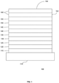
- FIG. 1 shows an organic light emitting device 100.
- Device 100 may include a substrate 110, an anode 115, a hole injection layer 120, a hole transport layer 125, an electron blocking layer 130, an emissive layer 135, a hole blocking layer 140, an electron transport layer 145, an electron injection layer 150, a protective layer 155, a cathode 160, and a barrier layer 170.
- Cathode 160 is a compound cathode having a first conductive layer 162 and a second conductive layer 164.
- Device 100 may be fabricated by depositing the layers described, in order. The properties and functions of these various layers, as well as example materials, are described in more detail in US 7,279,704 at cols. 6-10, which are incorporated by reference.
- each of these layers are available.
- a flexible and transparent substrate-anode combination is disclosed in U.S. Pat. No. 5,844,363 , which is incorporated by reference in its entirety.
- An example of a p-doped hole transport layer is m-MTDATA doped with F 4 -TCNQ at a molar ratio of 50:1, as disclosed in U.S. Patent Application Publication No. 2003/0230980 , which is incorporated by reference in its entirety.
- Examples of emissive and host materials are disclosed in U.S. Pat. No. 6,303,238 to Thompson et al. , which is incorporated by reference in its entirety.
- An example of an n-doped electron transport layer is BPhen doped with Li at a molar ratio of 1:1, as disclosed in U.S. Patent Application Publication No. 2003/0230980 , which is incorporated by reference in its entirety.
- U.S. Pat. Nos. 5,703,436 and 5,707,745 which are incorporated by reference in their entireties, disclose examples of cathodes including compound cathodes having a thin layer of metal such as Mg:Ag with an overlying transparent, electrically-conductive, sputter-deposited ITO layer.
- the theory and use of blocking layers is described in more detail in U.S. Pat. No. 6,097,147 and U.S. Patent Application Publication No.
- FIG. 2 shows an inverted OLED 200.
- the device includes a substrate 210, a cathode 215, an emissive layer 220, a hole transport layer 225, and an anode 230.
- Device 200 may be fabricated by depositing the layers described, in order. Because the most common OLED configuration has a cathode disposed over the anode, and device 200 has cathode 215 disposed under anode 230, device 200 may be referred to as an "inverted" OLED. Materials similar to those described with respect to device 100 may be used in the corresponding layers of device 200.
- FIG. 2 provides one example of how some layers may be omitted from the structure of device 100.
- FIGS. 1 and 2 The simple layered structure illustrated in FIGS. 1 and 2 is provided by way of nonlimiting example, and it is understood that embodiments of the invention may be used in connection with a wide variety of other structures.
- the specific materials and structures described are exemplary in nature, and other materials and structures may be used.
- Functional OLEDs may be achieved by combining the various layers described in different ways, or layers may be omitted entirely, based on design, performance, and cost factors. Other layers not specifically described may also be included. Materials other than those specifically described may be used. Although many of the examples provided herein describe various layers as comprising a single material, it is understood that combinations of materials, such as a mixture of host and dopant, or more generally a mixture, may be used. Also, the layers may have various sublayers.
- hole transport layer 225 transports holes and injects holes into emissive layer 220, and may be described as a hole transport layer or a hole injection layer.
- an OLED may be described as having an "organic layer" disposed between a cathode and an anode. This organic layer may comprise a single layer, or may further comprise multiple layers of different organic materials as described, for example, with respect to FIGS. 1 and 2 .
- OLEDs comprised of polymeric materials (PLEDs) such as disclosed in U.S. Pat. No. 5,247,190 to Friend et al. , which is incorporated by reference in its entirety.
- PLEDs polymeric materials
- OLEDs having a single organic layer may be used.
- OLEDs may be stacked, for example as described in U.S. Pat. No. 5,707,745 to Forrest et al , which is incorporated by reference in its entirety.
- the OLED structure may deviate from the simple layered structure illustrated in FIGS. 1 and 2 .
- the substrate may include an angled reflective surface to improve out-coupling, such as a mesa structure as described in U.S. Pat. No. 6,091,195 to Forrest et al. , and/or a pit structure as described in U.S. Pat. No. 5,834,893 to Bulovic et al. , which are incorporated by reference in their entireties.
- any of the layers of the various embodiments may be deposited by any suitable method.
- preferred methods include thermal evaporation, ink-jet, such as described in U.S. Pat. Nos. 6,013,982 and 6,087,196 , which are incorporated by reference in their entireties, organic vapor phase deposition (OVPD), such as described in U.S. Pat. No. 6,337,102 to Forrest et al. , which is incorporated by reference in its entirety, and deposition by organic vapor jet printing (OVJP), such as described in U.S. Pat. No. 7,431,968 , which is incorporated by reference in its entirety.
- OVPD organic vapor phase deposition
- OJP organic vapor jet printing
- Other suitable deposition methods include spin coating and other solution based processes.
- Solution based processes are preferably carried out in nitrogen or an inert atmosphere.
- preferred methods include thermal evaporation.
- Preferred patterning methods include deposition through a mask, cold welding such as described in U.S. Pat. Nos. 6,294,398 and 6,468,819 , which are incorporated by reference in their entireties, and patterning associated with some of the deposition methods such as ink-jet and OVJD. Other methods may also be used.
- the materials to be deposited may be modified to make them compatible with a particular deposition method. For example, substituents such as alkyl and aryl groups, branched or unbranched, and preferably containing at least 3 carbons, may be used in small molecules to enhance their ability to undergo solution processing.
- Substituents having 20 carbons or more may be used, and 3-20 carbons is a preferred range. Materials with asymmetric structures may have better solution processibility than those having symmetric structures, because asymmetric materials may have a lower tendency to recrystallize. Dendrimer substituents may be used to enhance the ability of small molecules to undergo solution processing.
- Devices fabricated in accordance with embodiments of the present invention may further optionally comprise a barrier layer.
- a barrier layer One purpose of the barrier layer is to protect the electrodes and organic layers from damaging exposure to harmful species in the environment including moisture, vapor and/or gases, etc.
- the barrier layer may be deposited over, under or next to a substrate, an electrode, or over any other parts of a device including an edge.
- the barrier layer may comprise a single layer, or multiple layers.
- the barrier layer may be formed by various known chemical vapor deposition techniques and may include compositions having a single phase as well as compositions having multiple phases. Any suitable material or combination of materials may be used for the barrier layer.
- the barrier layer may incorporate an inorganic or an organic compound or both.
- the preferred barrier layer comprises a mixture of a polymeric material and a non-polymeric material as described in U.S. Pat. No. 7,968,146 , PCT Pat. Application Nos. PCT/US2007/023098 and PCT/US2009/042829 , which are herein incorporated by reference in their entireties.
- the aforesaid polymeric and non-polymeric materials comprising the barrier layer should be deposited under the same reaction conditions and/or at the same time.
- the weight ratio of polymeric to non-polymeric material may be in the range of 95:5 to 5:95.
- the polymeric material and the non-polymeric material may be created from the same precursor material.
- the mixture of a polymeric material and a non-polymeric material consists essentially of polymeric silicon and inorganic silicon.
- Devices fabricated in accordance with embodiments of the invention can be incorporated into a wide variety of electronic component modules (or units) that can be incorporated into a variety of electronic products or intermediate components. Examples of such electronic products or intermediate components include display screens, lighting devices such as discrete light source devices or lighting panels, etc. that can be utilized by the end-user product manufacturers. Such electronic component modules can optionally include the driving electronics and/or power source(s). Devices fabricated in accordance with embodiments of the invention can be incorporated into a wide variety of consumer products that have one or more of the electronic component modules (or units) incorporated therein. Such consumer products would include any kind of products that include one or more light source(s) and/or one or more of some type of visual displays.
- Some examples of such consumer products include flat panel displays, computer monitors, medical monitors, televisions, billboards, lights for interior or exterior illumination and/or signaling, heads-up displays, fully or partially transparent displays, flexible displays, laser printers, telephones, cell phones, tablets, phablets, personal digital assistants (PDAs), laptop computers, digital cameras, camcorders, viewfinders, micro-displays, 3-D displays, vehicles, a large area wall, theater or stadium screen, or a sign.
- PDAs personal digital assistants
- Various control mechanisms may be used to control devices fabricated in accordance with the present invention, including passive matrix and active matrix. Many of the devices are intended for use in a temperature range comfortable to humans, such as 18 degrees C. to 30 degrees C., and more preferably at room temperature (20-25 degrees C), but could be used outside this temperature range, for example, from -40 degree C to + 80 degree C.
- the materials and structures described herein may have applications in devices other than OLEDs.
- other optoelectronic devices such as organic solar cells and organic photodetectors may employ the materials and structures.
- organic devices such as organic transistors, may employ the materials and structures.
- halo includes fluorine, chlorine, bromine, and iodine.
- alkyl as used herein contemplates both straight and branched chain alkyl radicals.
- Preferred alkyl groups are those containing from one to fifteen carbon atoms and includes methyl, ethyl, propyl, isopropyl, butyl, isobutyl, tert-butyl, and the like. Additionally, the alkyl group may be optionally substituted.
- cycloalkyl as used herein contemplates cyclic alkyl radicals.
- Preferred cycloalkyl groups are those containing 3 to 7 carbon atoms and includes cyclopropyl, cyclopentyl, cyclohexyl, and the like. Additionally, the cycloalkyl group may be optionally substituted.
- alkenyl as used herein contemplates both straight and branched chain alkene radicals.
- Preferred alkenyl groups are those containing two to fifteen carbon atoms. Additionally, the alkenyl group may be optionally substituted.
- alkynyl as used herein contemplates both straight and branched chain alkyne radicals. Preferred alkynyl groups are those containing two to fifteen carbon atoms. Additionally, the alkynyl group may be optionally substituted.
- aralkyl or "arylalkyl” as used herein are used interchangeably and contemplate an alkyl group that has as a substituent an aromatic group. Additionally, the aralkyl group may be optionally substituted.
- heterocyclic group contemplates aromatic and non-aromatic cyclic radicals.
- Hetero-aromatic cyclic radicals also means heteroaryl.
- Preferred hetero-non-aromatic cyclic groups are those containing 3 or 7 ring atoms which includes at least one hetero atom, and includes cyclic amines such as morpholino, piperdino, pyrrolidino, and the like, and cyclic ethers, such as tetrahydrofuran, tetrahydropyran, and the like. Additionally, the heterocyclic group may be optionally substituted.
- aryl or "aromatic group” as used herein contemplates single-ring groups and polycyclic ring systems having 6 to 30 carbon atoms in the rings, preferably 6 to 18 carbons.
- the polycyclic rings may have two or more rings in which two carbons are common to two adjoining rings (the rings are "fused") wherein at least one of the rings is aromatic, e.g., the other rings can be cycloalkyls, cycloalkenyls, aryl, heterocycles, and/or heteroaryls. Additionally, the aryl group may be optionally substituted.
- heteroaryl as used herein includes hetero-aromatic groups that may include 3 to 30 carbon atoms, preferably 3 to 18 carbons in the ring and contemplates single-ring hetero-aromatic groups that may include from one to three heteroatoms, for example, pyrrole, furan, thiophene, imidazole, oxazole, thiazole, triazole, pyrazole, pyridine, pyrazine and pyrimidine, and the like.
- heteroaryl also includes polycyclic hetero-aromatic systems having two or more rings in which two atoms are common to two adjoining rings (the rings are "fused") wherein at least one of the rings is a heteroaryl, e.g., the other rings can be cycloalkyls, cycloalkenyls, aryl, heterocycles, and/or heteroaryls. Additionally, the heteroaryl group may be optionally substituted.
- alkyl, cycloalkyl, alkenyl, alkynyl, aralkyl, heterocyclic group, aryl, and heteroaryl may be optionally substituted with one or more substituents selected from the group consisting of hydrogen, deuterium, halogen, alkyl, cycloalkyl, heteroalkyl, arylalkyl, alkoxy, aryloxy, amino, cyclic amino, silyl, alkenyl, cycloalkenyl, heteroalkenyl, alkynyl, aryl, heteroaryl, acyl, carbonyl, carboxylic acid, ether, ester, nitrile, isonitrile, sulfanyl, sulfinyl, sulfonyl, phosphino, and combinations thereof.
- substituted indicates that a substituent other than H is bonded to the relevant position, such as carbon.
- substituent other than H such as carbon.
- R 1 is mono-substituted
- one R 1 must be other than H.
- R 1 is di-substituted
- two of R 1 must be other than H.
- R 1 is hydrogen for all available positions.
- aza-dibenzofuran i.e. aza-dibenzofuran, aza-dibenzothiophene, etc.
- azatriphenylene encompasses both dibenzo[ f , h ]quinoxaline and dibenzo[ f , h ]quinoline.
- a composition comprising a novel first compound, wherein the first compound is capable of functioning as a phosphorescent emitter in an organic light emitting device at room temperature.
- the first compound has at least one aromatic ring and at least one substituent R, wherein each of the at least one substituent R is independently selected from the group consisting of partially fluorinated alkyl, partially fluorinated cycloalkyl, and combinations thereof; wherein each of the at least one substituent R is directly bonded to one of the aromatic rings, and wherein in each of the at least one substituent R, C having an F attached thereto is separated by at least one carbon atom from the aromatic ring.
- Each of the at least one substituent R being directly bonded to one of the aromatic rings means that each R can be bonded to different aromatic rings or some of the Rs can be bonded to the same aromatic ring.
- Partially fluorinated group means that not all of the carbon-hydrogen bonds in a group have been replaced by carbon-flurine bonds, in other words, there is at least one carbon-hydrogen bond remaining in that group.
- the first compound is capable of emitting light from a triplet excited state to a ground singlet state at room temperature.
- the first compound is a metal coordination complex having a metal-carbon bond.
- the metal can be selected from the group consisting of Ir, Rh, Re, Ru, Os, Pt, Au, and Cu. In one preferred embodiment, the metal is Ir. In another preferred embodiment, the metal is Pt.
- C having an F attached thereto is separated by at least two carbon atoms from the aromatic ring. In another embodiment, C having an F attached thereto is separated by at least three carbon atoms from the aromatic ring.
- each of the at least one substituent R contains at least one CF 3 group. In a preferred embodiment, each of the at least one substituent R contains only CF 3 group and no CF or CF 2 groups. In another embodiment, none of the at least one substituent R contain any CF 3 groups.
- the first compound does not have any F atoms other than those in the at least one substituent R.
- the aromatic ring comprises LUMO electron density of the first compound.
- m in the formula C n H 2n+1-m F m and C q H 2q - 1-m F m is not a multiple of 3. In another embodiment, m is a multiple of 3.
- the first compound as defined above has the formula of M(L 1 ) x (L 2 ) y (L 3 ) z ; wherein L 1 , L 2 , and L 3 can be the same or different;
- M is Ir and the first compound has the formula of Ir(L 1 ) 2 (L 2 ).
- L 1 has the formula selected from the group consisting of: and L 2 has the formula: wherein R a , R b , and R c independently represent mono, di, tri, or tetra substitution, or no substitution;
- M is Ir and the first compound has the formula of Ir(L 1 ) 2 (L 2 ) where L 1 has the formula selected from the group consisting of: L 2 has the formula:
- L 1 and L 2 are different and each are independently selected from the group consisting of: and wherein at least one of R a and R b includes at least one R.
- L 1 and L 2 are each independently selected from the group consisting of: wherein at least one of R a , R b , and R c includes at least one R.
- the compound can have the formula of Pt(L 1 ) 2 or Pt(L 1 )(L 2 ).
- L 1 can be connected to the other L 1 .
- L 1 can be connected to L 2 to form a tetradentate ligand.
- at least one of R a , R b , R c , and R d includes an alkyl or cycloalkyl group that includes CD, CD 2 , or CD 3 , wherein D is deuterium.
- L 1 , L 2 , and L 3 can be the same or different;
- L 1 is selected from the group consisting of L A1 through L A450 , and L A451
- L 2 is selected from the group consisting of
- dash line represents the bond between the current group and the next group to which it attaches.
- dash lines represent the bonds between the M and the ligand; in R A1 , dash line represents the bond between R and the aromatic ring.
- L A1 through L A451 and L B1 through L B13 are as defined above.
- the examples of the first compound disclosed herein are metal complexes based on ligands containing 1-phenylisoquinoline, 2-phenylquinoline, 8-(quinolin-2-yl)benzofuro[2,3-b]pyridine, 8-(isoquinolin-1-yl)benzofuro[2,3-b]pyridine, 4-(4-fluorophenyl)quinazoline, or 2-phenylpyridine, etc.
- Each of the ligands contain at least one alkylated side chain which contains at least one fluorine atom that is not benzylic. The presence of these side chains provide a fine tuning of the color of the metal complex mostly as a slight red shift.
- a first device comprising a first organic light emitting device.
- the first organic light emitting device comprises: an anode; a cathode; and an organic layer, disposed between the anode and the cathode.
- the organic layer comprises the first compound as disclosed herein.
- the first compound incorporated into the first device can be any one or more of the embodiments and variations of the first compound disclosed herein.
- the first compound is capable of functioning as a phosphorescent emitter at room temperature and wherein the first compound has at least one aromatic ring and at least one substituent R, wherein each of the at least one substituent R is independently selected from the group consisting of partially fluorinated alkyl, partially fluorinated cycloalkyl, and combinations thereof; wherein each of the at least one substituent R is directly bonded to one of the aromatic rings; and wherein in each of the at least one substituent R, C having an F attached thereto is separated by at least one carbon atom from the aromatic ring.
- the first device is selected from the group consisting of a consumer product, an electronic component module, an organic light emitting device, and a lighting panel.
- the organic layer is an emissive layer and the compound is an emissive dopant.
- the host in the first device can comprise at least one chemical group selected from the group consisting of triphenylene, carbazole, dibenzothiphene, dibenzofuran, dibenzoselenophene, azatriphenylene, azacarbazole, aza-dibenzothiophene, aza-dibenzofuran, and aza-dibenzoselenophene.
- the host can be selected from the group consisting of: and combinations thereof.
- a formulation that comprises the compound having at least one non-conjugated substituent R selected from the group consisting of C n H 2n+1-m F m and C q H 2q-1-m F m , wherein R is directly bonded to an aromatic ring.
- R is directly bonded to an aromatic ring.
- n is an integer greater than 1
- q is an integer greater than 2
- m is an integer greater than 0, wherein C having F attaching to is separated by at least one carbon atom from the aromatic ring
- the formulation can also include one or more components selected from the group consisting of a solvent, a host, a hole injection material, hole transport material, and an electron transport layer material, disclosed herein.
- the Ir(III) Dimer (1.08 g, 0.65 mmol) and 3,7-diethylnonane-4,6-dione (1.38 g, 6.52 mmol) were diluted in ethoxyethanol (22 mL) and the mixture was degassed by bubbling nitrogen gas for 15 minutes. K 2 CO 3 (0.90 g, 6.52 mmol) was then added and the reaction was stirred at room temperature overnight. The mixture was diluted with dichloromethane (“DCM”), filtered through a pad of Celite, and washed with DCM. The crude material was purified by column chromatography (silica pre-treated with triethylamine (TEA)) using Heptanes/DCM 80/20 solvent system. The collected pure fractions were triturated from methanol and the solids were recrystallized from dichloromethane/methanol to afford the Comparative Compound 1 (0.85 g, 65 % yield) as a dark red powder.
- DCM dichloromethane
- the reaction mixture was quenched with aqueous ammonium chloride then was extracted 2 X 200 mL of ethyl acetate, and dried over sodium sulfate.
- the crude material was coated on Celite and purified by column chromatography using a 20% DCM in Heptanes solvent system. The product was recrystallized in heptanes to afford 0.90 g of the target compound (81% yield).
- the Ir(III) Dimer (0.95 g, 0.537 mmol) and 3,7-diethylnonane-4,6-dione (1.14 g, 5.37 mmol) were diluted in ethoxyethanol (15 mL) and the mixture was degassed by bubbling nitrogen gas for 15 minutes. K 2 CO 3 (0.74 g, 5.37 mmol) was then added and the reaction was stirred at room temperature overnight. The mixture was diluted with DCM, filtered through a pad of Celite, and washed with DCM. The crude material was purified by column chromatography (silica pre-treated with TEA) using Heptanes/DCM (100/0 to 97/3) solvent system. The collected pure fractions were triturated from methanol and the solids were recrystallized from dichloromethane/methanol to afford Compound 453 (0.83 g, 73 % yield) as a dark red powder.
- the Ir(III) Dimer (1.00 g, 0.47 mmol) and 3,7-diethylnonane-4,6-dione (0.91 g, 4.26 mmol) were diluted in 2-Ethoxyethanol (14 mL) and the mixture was degassed by bubbling nitrogen gas for 15 minutes. K 2 CO 3 (0.59 g, 4.26 mmol) was then added and the reaction was stirred at room temperature overnight. The mixture was diluted with dichloromethane, filtered through a pad of Celite, and washed with DCM. T he crude material was purified by column chromatography (silica pre-treated with TEA) using Heptanes/ dichloromethane 80/20 solvent system. The combined fractions were triturated from methanol and the solids were recrystallized from dichloromethane /methanol once. The title product was obtained as a red powder (0.8 g, 76% yield).
- the reaction was diluted with ethyl acetate, water and brine.
- the aqueous was partitioned off and the organic was washed once with brine, dried with sodium sulfate, filtered then concentrated down to a yellow solid.
- the yellow solid was purified with silica gel using DCM to 85/15 DCM/ethyl acetate solvent system to get 4.1 g of light yellow solid for a 71% yield.
- the dimer (1.50 g, 0.81 mmol), 3,7-diethylnonane-4,6-dione (1.73 g, 8.13 mmol), and 2-ethoxyethanol (50ml) were combined round bottom flask. Nitrogen was bubbled directly into the suspension for 15 min. Potassium carbonate (1.12 g, 8.13 mmol) was added and the reaction was run at room temperature overnight. Upon completion, the reaction was filtered through celite using DCM until the red color came off. The solution was concentrated down to a dark red oily solid, taken up in DCM and adsorbed on to celite. The sample was purified with silica gelto give 0.24 g of dark red solid for a 13% yield.
- Lithium chloride (1.87 g, 44.1 mmol) was charged into a reaction flask. The flask was evacuated and heated using a heat gun for 10 minutes. The flask was cooled to room temperature and zinc (2.88 g, 44.1 mmol) was added to the flask. The flask was again evacuated and heated using a heat gun for 10 minutes. The flask was cooled to room temperature and THF (80 mL) was syringed into the reaction followed by 1,2-dibromoethane (0.42 mL, 4.90 mmol). This mixture was stirred for 30 minutes in an oil bath set at 60°C.
- the Ir(III) Dimer (0.50 g, 0.24 mmol) was solubilized in Ethoxyethanol (8 mL) and pentane-2,4-dione (0.25 mL, 2.39 mmol) was added. The mixture was degassed by bubbling nitrogen gas for 15 minutes and K 2 CO 3 (0.33 g, 2.39 mmol) was then added and the reaction was stirred at room temperature overnight. Upon completion of the reaction, the mixture was diluted with DCM, filtered through celite and washed with DCM. The crude product was coated on Celite and purified via column chromatography (TEA pretreated) using Heptanes/DCM (95/5) solvent system. The product was recrystallized several times (5 times) from MeOH/DCM, EtOH/DCM, and THF/i-PrOH to afford 0.18 g (34% yield) of the target compound.
- the Ir(III) Dimer (0.70 g, 0.33 mmol) was solubilized in Ethoxyethanol (15 mL) and 3,7-diethylnonane-4,6-dione (0.71 g, 3.34 mmol) was added. The mixture was degassed by bubbling nitrogen gas for 15 minutes and K 2 CO 3 (0.46 g, 3.34 mmol) was then added and the reaction was stirred at room temperature overnight. Upon completion of the reaction, the mixture was diluted with DCM, filtered through celite and washed with DCM. The crude product was coated on Celite and purified via column chromatography (TEA pretreated) using Heptanes/DCM (95/5 to 90/10) solvent system. The product was triturated from methanol to afford 0.21 g (26% yield) of the dopant.
- the materials described herein as useful for a particular layer in an organic light emitting device may be used in combination with a wide variety of other materials present in the device.
- emissive dopants disclosed herein may be used in conjunction with a wide variety of hosts, transport layers, blocking layers, injection layers, electrodes and other layers that may be present.
- the materials described or referred to below are non-limiting examples of materials that may be useful in combination with the compounds disclosed herein, and one of skill in the art can readily consult the literature to identify other materials that may be useful in combination.
- a hole injecting/transporting material to be used in the present invention is not particularly limited, and any compound may be used as long as the compound is typically used as a hole injecting/transporting material.
- the material include, but not limit to: a phthalocyanine or porphyrin derivative; an aromatic amine derivative; an indolocarbazole derivative; a polymer containing fluorohydrocarbon; a polymer with conductivity dopants; a conducting polymer, such as PEDOT/PSS; a self-assembly monomer derived from compounds such as phosphonic acid and silane derivatives; a metal oxide derivative, such as MoO x ; a p-type semiconducting organic compound, such as 1,4,5,8,9,12-Hexaazatriphenylenehexacarbonitrile; a metal complex, and a cross-linkable compounds.
- aromatic amine derivatives used in HIL or HTL include, but not limit to the following general structures:
- Each of Ar 1 to Ar 9 is selected from the group consisting of aromatic hydrocarbon cyclic compounds such as benzene, biphenyl, triphenyl, triphenylene, naphthalene, anthracene, phenalene, phenanthrene, fluorene, pyrene, chrysene, perylene, and azulene; the group consisting of aromatic heterocyclic compounds such as dibenzothiophene, dibenzofuran, dibenzoselenophene, furan, thiophene, benzofuran, benzothiophene, benzoselenophene, carbazole, indolocarbazole, pyridylindole, pyrrolodipyridine, pyrazole, imidazole, triazole, oxazole, thiazole, oxadiazole, oxatriazole, dioxazole, thiadiazole, pyridine, pyridazine
- each Ar is further substituted by a substituent selected from the group consisting of hydrogen, deuterium, halide, alkyl, cycloalkyl, heteroalkyl, arylalkyl, alkoxy, aryloxy, amino, silyl, alkenyl, cycloalkenyl, heteroalkenyl, alkynyl, aryl, heteroaryl, acyl, carbonyl, carboxylic acids, ester, nitrile, isonitrile, sulfanyl, sulfinyl, sulfonyl, phosphino, and combinations thereof.
- a substituent selected from the group consisting of hydrogen, deuterium, halide, alkyl, cycloalkyl, heteroalkyl, arylalkyl, alkoxy, aryloxy, amino, silyl, alkenyl, cycloalkenyl, heteroalkenyl, alkynyl, aryl, heteroaryl, acy
- Ar 1 to Ar 9 is independently selected from the group consisting of: wherein k is an integer from 1 to 20; X 101 to X 108 is C (including CH) or N; Z 101 is NAr 1 , O, or S; Ar 1 has the same group defined above.
- metal complexes used in HIL or HTL include, but not limit to the following general formula: wherein Met is a metal, which can have an atomic weight greater than 40; (Y 101 -Y 102 ) is a bidentate ligand, Y 101 and Y 102 are independently selected from C, N, O, P, and S; L 101 is an ancillary ligand; k' is an integer value from 1 to the maximum number of ligands that may be attached to the metal; and k'+k" is the maximum number of ligands that may be attached to the metal.
- (Y 101 -Y 102 ) is a 2-phenylpyridine derivative. In another aspect, (Y 101 -Y 102 ) is a carbene ligand. In another aspect, Met is selected from Ir, Pt, Os, and Zn. In a further aspect, the metal complex has a smallest oxidation potential in solution vs. Fc + /Fc couple less than about 0.6 V.
- the light emitting layer of the organic EL device of the present invention preferably contains at least a metal complex as light emitting material, and may contain a host material using the metal complex as a dopant material.
- the host material are not particularly limited, and any metal complexes or organic compounds may be used as long as the triplet energy of the host is larger than that of the dopant. While the Table below categorizes host materials as preferred for devices that emit various colors, any host material may be used with any dopant so long as the triplet criteria is satisfied.
- Examples of metal complexes used as host are preferred to have the following general formula: wherein Met is a metal; (Y 103 -Y 104 ) is a bidentate ligand, Y 103 and Y 104 are independently selected from C, N, O, P, and S; L 101 is an another ligand; k' is an integer value from 1 to the maximum number of ligands that may be attached to the metal; and k'+k" is the maximum number of ligands that may be attached to the metal.
- the metal complexes are: wherein (O-N) is a bidentate ligand, having metal coordinated to atoms O and N.
- Met is selected from Ir and Pt.
- (Y 103 -Y 104 ) is a carbene ligand.
- organic compounds used as host are selected from the group consisting of aromatic hydrocarbon cyclic compounds such as benzene, biphenyl, triphenyl, triphenylene, naphthalene, anthracene, phenalene, phenanthrene, fluorene, pyrene, chrysene, perylene, and azulene; the group consisting of aromatic heterocyclic compounds such as dibenzothiophene, dibenzofuran, dibenzoselenophene, furan, thiophene, benzofuran, benzothiophene, benzoselenophene, carbazole, indolocarbazole, pyridylindole, pyrrolodipyridine, pyrazole, imidazole, triazole, oxazole, thiazole, oxadiazole, oxatriazole, dioxazole, thiadiazole, pyridine, pyridazine,
- each group is further substituted by a substituent selected from the group consisting of hydrogen, deuterium, halide, alkyl, cycloalkyl, heteroalkyl, arylalkyl, alkoxy, aryloxy, amino, silyl, alkenyl, cycloalkenyl, heteroalkenyl, alkynyl, aryl, heteroaryl, acyl, carbonyl, carboxylic acids, ester, nitrile, isonitrile, sulfanyl, sulfinyl, sulfonyl, phosphino, and combinations thereof.
- a substituent selected from the group consisting of hydrogen, deuterium, halide, alkyl, cycloalkyl, heteroalkyl, arylalkyl, alkoxy, aryloxy, amino, silyl, alkenyl, cycloalkenyl, heteroalkenyl, alkynyl, aryl, heteroaryl, acy
- the host compound contains at least one of the following groups in the molecule:
- a hole blocking layer may be used to reduce the number of holes and/or excitons that leave the emissive layer.
- the presence of such a blocking layer in a device may result in substantially higher efficiencies as compared to a similar device lacking a blocking layer.
- a blocking layer may be used to confine emission to a desired region of an OLED.
- compound used in HBL contains the same molecule or the same functional groups used as host described above.
- compound used in HBL contains at least one of the following groups in the molecule: wherein k is an integer from 1 to 20; L 101 is an another ligand, k' is an integer from 1 to 3.
- Electron transport layer may include a material capable of transporting electrons. Electron transport layer may be intrinsic (undoped), or doped. Doping may be used to enhance conductivity. Examples of the ETL material are not particularly limited, and any metal complexes or organic compounds may be used as long as they are typically used to transport electrons.
- compound used in ETL contains at least one of the following groups in the molecule: wherein R 101 is selected from the group consisting of hydrogen, deuterium, halide, alkyl, cycloalkyl, heteroalkyl, arylalkyl, alkoxy, aryloxy, amino, silyl, alkenyl, cycloalkenyl, heteroalkenyl, alkynyl, aryl, heteroaryl, acyl, carbonyl, carboxylic acids, ester, nitrile, isonitrile, sulfanyl, sulfinyl, sulfonyl, phosphino, and combinations thereof, when it is aryl or heteroaryl, it has the similar definition as Ar's mentioned above.
- Ar 1 to Ar 3 has the similar definition as Ar's mentioned above.
- k is an integer from 1 to 20.
- X 101 to X 108 is selected from C (including CH) or N.
- the metal complexes used in ETL contains, but not limit to the following general formula: wherein (O-N) or (N-N) is a bidentate ligand, having metal coordinated to atoms O, N or N, N; L 101 is another ligand; k' is an integer value from 1 to the maximum number of ligands that may be attached to the metal.
- the hydrogen atoms can be partially or fully deuterated.
- any specifically listed substituent such as, without limitation, methyl, phenyl, pyridyl, etc. encompasses undeuterated, partially deuterated, and fully deuterated versions thereof.
- classes of substituents such as, without limitation, alkyl, aryl, cycloalkyl, heteroaryl, etc. also encompass undeuterated, partially deuterated, and fully deuterated versions thereof.
- hole injection materials In addition to and / or in combination with the materials disclosed herein, many hole injection materials, hole transporting materials, host materials, dopant materials, exiton/hole blocking layer materials, electron transporting and electron injecting materials may be used in an OLED.
- Non-limiting examples of the materials that may be used in an OLED in combination with materials disclosed herein are listed in Table A below. Table A lists non-limiting classes of materials, non-limiting examples of compounds for each class, and references that disclose the materials. TABLE A MATERIAL EXAMPLES OF MATERIAL PUBLICATIONS Hole injection materials Phthalocyanine and porphyrin compounds Appl. Phys. Lett. 69, 2160 (1996 ) Starburst triarylamines J. Lumin.
- All example devices were fabricated by high vacuum ( ⁇ 10 -7 Torr) thermal evaporation.
- the anode electrode was 1200 ⁇ of indium tin oxide (ITO).
- the cathode consisted of 10 ⁇ of LiF followed by 1,000 ⁇ of Al. All devices were encapsulated with a glass lid sealed with an epoxy resin in a nitrogen glove box ( ⁇ 1 ppm of H 2 O and O 2 ) immediately after fabrication, and a moisture getter was incorporated inside the package.
- the organic stack of the device examples consisted of sequentially, from the ITO surface, 100 ⁇ of LG101(purchased from LG chem) as the hole injection layer (HIL); 400 ⁇ of 4,4'-bis[N-(1-naphthyl)-N-phenylamino]biphenyl (NPD) as the hole transporting layer (HTL); 300 ⁇ of an emissive layer (EML) containing Compound H as a host (79%), a stability dopant (SD) (18%), and Compound 453, Compound 781, or Compound 699 as an emitter; 100 ⁇ of Compound H as a blocking layer; and 450 ⁇ of Alq 3 (tris-8-hydroxyquinoline aluminum) as the ETL.
- HIL hole injection layer
- NPD 4,4'-bis[N-(1-naphthyl)-N-phenylamino]biphenyl
- HTL hole transporting layer
- EML emissive layer
- SD stability do
- the emitter was selected to provide the desired color and the stability dopant (SD) was mixed with the electron-transporting host and the emitter to help transport positive charge in the emissive layer.
- the Comparative Example device was fabricated similarly to the device examples except that Comparative Compound 1 was used as the emitter in the EML. Table 1 shows the composition of the EML in the device, while the device results and data are summarized in Table 2.
- NPD, compound H, SD, and AlQ 3 have the following structures:
- Comparative Compound 1 used in the experiments has the following structure
- Inventive Compounds Representative inventive compounds Compound 453, Compound 781, Compound 699, Compound 22, and Compound 473 used in the experiments have the following structures:
- Table 1 below lists the compounds used as the emitter dopants in the EML layer of the experimental devices. Table 1 Example Emitter Inventive Device Example 1 Compound 453 Inventive Device Example 2 Compound 781 Inventive Device Example 3 Compound 699 Inventive Device Example 4 Compound 22 Inventive Device Example 5 Compound 473 Comparative Device example 1 Comparative compound 1
- Table 2 below provides the device performance data for Inventive Device Examples 1, 2, 3, 4 and 5 and Comparative Device example 1.
- Table 2 1931 CIE ⁇ max [nm] EQE at 1,000 nits [cd/A] LT 95% at 1,000 nits [h]
- X y Inventive Device Example 1 0.65 0.35 620 1.74 8.55 Inventive Device Example 2 0.64 0.36 614 1.74 9.09
- Inventive Device Example 3 0.66 0.34 618 1.82 5.73
- Inventive Device Example 4 0.65 0.35 627 1.64 1.53
- Inventive Device Example 5 0.65 0.35 624 1.80 1.54 Comparative example 1 0.66 0.34 644 1.00 1.00
- Table 2 summarizes the performance of the experimental devices.
- the 1931 CIE values were measured at 10 mA/cm 2 .
- the luminous efficiency was measured at 1000 cd/m 2 .
- the EQE, and LT 95% of comparative example 1 were set at a value of 1.00.
- the values obtained from the inventive examples are relative to that of the comparative example. All of the Inventive Device Examples exhibit higher external quantum efficiencies (EQE) than the Comparative example 1 (1.74, 1.74, 1.82, 1.64, 1.80 vs. 1.00).
- a composition comprising a first compound; wherein the first compound is capable of functioning as a phosphorescent emitter in an organic light emitting device at room temperature; wherein the first compound has at least one aromatic ring and at least one substituent R; wherein each of the at least one R is independently selected from the group consisting of partially fluorinated alkyl, partially fluorinated cycloalkyl, and combinations thereof; wherein each of the at least one R is directly bonded to one of the aromatic rings;and wherein in each of the at least one R, C having an F attached thereto is separated by at least one carbon atom from the aromatic ring.
- the first compound is capable of emitting light from a triplet excited state to a ground singlet state at room temperature.
- the composition of paragraph 1, wherein the first compound is a metal coordination complex having a metal-carbon bond. 4.
- the composition of paragraph 3, wherein the metal is selected from the group consisting of Ir, Rh, Re, Ru, Os, Pt, Au, and Cu. 5.
- the composition of paragraph 3, wherein the metal is Ir. 6.
- the composition of paragraph 3, wherein the metal is Pt. 7.
- the composition of paragraph 1, wherein C having an F attached thereto is separated by at least two carbon atoms from the aromatic ring.
- C having an F attached thereto is separated by at least three carbon atoms from the aromatic ring.
- each of the at least one R contains at least one CF 3 group. 10.
- composition of paragraph 1 wherein none of the at least one R contain any CF 3 groups. 11.
- the aromatic ring comprises LUMO electron density of the first compound.
- the first compound has the formula of M(L 1 ) x (L 2 h,(L 3 ) z ; wherein L 1 , L 2 , and L 3 can be the same or different; wherein x is 1, 2, or 3; wherein y is 0, 1, or 2; wherein z is 0, 1, or 2; wherein x+y+z is the oxidation state of the metal M; wherein L 1 , L 2 , and L 3 are each independently selected from the group consisting of: and wherein R a , R b , R c , and R d independently represent mono, di, tri, or tetra substitution, or no substitution; wherein R a , R b , R c , and R d are independently selected from the group consisting of hydrogen, deuterium, halide, alkyl, cycloalkyl, heteroalkyl, arylalkyl, alkoxy, aryloxy, amino, silyl, alkenyl,
- composition of paragraph 13 wherein the first compound has the formula of lr(L 1 ) 2 (L 2 ). 15. The composition of paragraph 14, wherein L 1 has the formula selected from the group consisting of: and wherein L 2 has the formula: 16. The composition of paragraph 15, wherein L 2 has the formula: wherein R e , R f , R h , and R i are independently selected from group consisting of alkyl, cycloalkyl, aryl, and heteroaryl; wherein at least one of R e , R f , R h , and R i has at least two carbon atoms; wherein R g is selected from group consisting of hydrogen, deuterium, halide, alkyl, cycloalkyl, heteroalkyl, arylalkyl, alkoxy, aryloxy, amino, silyl, alkenyl, cycloalkenyl, heteroalkenyl, alkynyl, aryl, heteroaryl, acyl, carbony
- composition of paragraph 14 wherein L 1 and L 2 are different and each independently selected from the group consisting of: and 18.
- the composition of paragraph 14, wherein L 1 and L 2 are each independently selected from the group consisting of: 19.
- the composition of paragraph 13, wherein the first compound has the formula of Pt(L 1 ) 2 or Pt(L 1 )(L 2 ).
- 20. The composition of paragraph 19, wherein L 1 is connected to the other L 1 or L 2 to form a tetradentate ligand.
- 21. The composition of paragraph 13, wherein at least one of R a , R b , R c , and R d includes an alkyl or cycloalkyl group that includes CD, CD 2 , or CD 3 , wherein D is deuterium. 22.
- the composition of paragraph 1, wherein the first compound has the formula of Ir(L 1 ) 2 (L 2 ), wherein L 1 is selected from the group consisting of wherein, R A1 through R A41 have the formulas: and wherein L 2 is selected from the group consisting of: 24.
- the compound of paragraph 23, wherein the first compound is selected from the group consisting of Compound 1 through Compound 5,863, wherein each of Compound x , where x 451 j + k ⁇ 451, k is an integer from 1 to 451, and j is an integer from 1 to 13, has the formula Ir(L A k ) 2 (L B j ). 25.
- the composition of paragraph 1, wherein the first compound is selected from the group consisting of 26.
- a first device comprising a first organic light emitting device, the first organic light emitting device comprising: an anode; a cathode; and an organic layer, disposed between the anode and the cathode, comprising a first compound, wherein the first compound is capable of functioning as a phosphorescent emitter at room temperature; wherein the first compound has at least one aromatic ring and at least one substituent R; wherein each of the at least one R is independently selected from the group consisting of partially fluorinated alkyl, partially fluorinated cycloalkyl, and combinations thereof; wherein each of the at least one R is directly bonded to one of the aromatic rings;and wherein in each of the at least one R, C having an F attached thereto is separated by at least one carbon atom from the aromatic ring.
- the first device of paragraph 26 wherein the first compound is selected from the group consisting of 28.
- the organic layer further comprises a host; wherein the host comprises at least one chemical group selected from the group consisting of triphenylene, carbazole, dibenzothiphene, dibenzofuran, dibenzoselenophene, azatriphenylene, azacarbazole, aza-dibenzothiophene, aza-dibenzofuran, and azadibenzoselenophene.
- the organic layer further comprises a host; wherein the host material is selected from the group consisting of : and combinations thereof.
- the organic layer further comprises a host; wherein the host material comprises a metal complex. 34.
- a formulation comprising the composition of paragraph 1.
Landscapes
- Chemical & Material Sciences (AREA)
- Engineering & Computer Science (AREA)
- Materials Engineering (AREA)
- Organic Chemistry (AREA)
- Inorganic Chemistry (AREA)
- Crystallography & Structural Chemistry (AREA)
- Optics & Photonics (AREA)
- Physics & Mathematics (AREA)
- Electroluminescent Light Sources (AREA)
- Plural Heterocyclic Compounds (AREA)
- Nitrogen Condensed Heterocyclic Rings (AREA)
- Peptides Or Proteins (AREA)
- Luminescent Compositions (AREA)
Applications Claiming Priority (2)
| Application Number | Priority Date | Filing Date | Title |
|---|---|---|---|
| US14/509,274 US9397302B2 (en) | 2014-10-08 | 2014-10-08 | Organic electroluminescent materials and devices |
| EP15185414.8A EP3007244B1 (en) | 2014-10-08 | 2015-09-16 | Organic electroluminescent materials and devices |
Related Parent Applications (1)
| Application Number | Title | Priority Date | Filing Date |
|---|---|---|---|
| EP15185414.8A Division EP3007244B1 (en) | 2014-10-08 | 2015-09-16 | Organic electroluminescent materials and devices |
Publications (1)
| Publication Number | Publication Date |
|---|---|
| EP3968404A1 true EP3968404A1 (en) | 2022-03-16 |
Family
ID=54150264
Family Applications (2)
| Application Number | Title | Priority Date | Filing Date |
|---|---|---|---|
| EP21204764.1A Pending EP3968404A1 (en) | 2014-10-08 | 2015-09-16 | Organic electroluminescent materials and devices |
| EP15185414.8A Active EP3007244B1 (en) | 2014-10-08 | 2015-09-16 | Organic electroluminescent materials and devices |
Family Applications After (1)
| Application Number | Title | Priority Date | Filing Date |
|---|---|---|---|
| EP15185414.8A Active EP3007244B1 (en) | 2014-10-08 | 2015-09-16 | Organic electroluminescent materials and devices |
Country Status (6)
| Country | Link |
|---|---|
| US (3) | US9397302B2 (ko) |
| EP (2) | EP3968404A1 (ko) |
| JP (4) | JP6640509B2 (ko) |
| KR (2) | KR102500262B1 (ko) |
| CN (3) | CN105503960A (ko) |
| TW (2) | TWI727933B (ko) |
Families Citing this family (37)
| Publication number | Priority date | Publication date | Assignee | Title |
|---|---|---|---|---|
| US9748500B2 (en) * | 2015-01-15 | 2017-08-29 | Universal Display Corporation | Organic light emitting materials |
| US10199581B2 (en) * | 2013-07-01 | 2019-02-05 | Universal Display Corporation | Organic electroluminescent materials and devices |
| US10003033B2 (en) * | 2014-02-18 | 2018-06-19 | Universal Display Corporation | Organic electroluminescent materials and devices |
| US10457699B2 (en) * | 2014-05-02 | 2019-10-29 | Universal Display Corporation | Organic electroluminescent materials and devices |
| US10854826B2 (en) | 2014-10-08 | 2020-12-01 | Universal Display Corporation | Organic electroluminescent compounds, compositions and devices |
| US9397302B2 (en) * | 2014-10-08 | 2016-07-19 | Universal Display Corporation | Organic electroluminescent materials and devices |
| US10411201B2 (en) * | 2014-11-12 | 2019-09-10 | Universal Display Corporation | Organic electroluminescent materials and devices |
| GB2536212A (en) * | 2015-03-04 | 2016-09-14 | Cambridge Display Tech Ltd | Light-emitting material and organic light-emitting device |
| US9871214B2 (en) * | 2015-03-23 | 2018-01-16 | Universal Display Corporation | Organic electroluminescent materials and devices |
| CN107464885B (zh) * | 2016-06-06 | 2019-01-18 | 清华大学 | 一种有机电致发光器件 |
| JP2018083941A (ja) * | 2016-11-14 | 2018-05-31 | 住友化学株式会社 | 組成物及びそれを用いた発光素子 |
| JP2018083940A (ja) * | 2016-11-14 | 2018-05-31 | 住友化学株式会社 | 組成物及びそれを用いた発光素子 |
| US11555048B2 (en) * | 2016-12-01 | 2023-01-17 | Universal Display Corporation | Organic electroluminescent materials and devices |
| US20180179237A1 (en) * | 2016-12-23 | 2018-06-28 | Universal Display Corporation | Organic electroluminescent materials and devices |
| US10862055B2 (en) * | 2017-05-05 | 2020-12-08 | Universal Display Corporation | Organic electroluminescent materials and devices |
| EP3418285B1 (en) | 2017-06-20 | 2020-05-06 | Idemitsu Kosan Co., Ltd. | Composition comprising a substituted ir complex and a phenylquinazoline bridged with a heteroatom |
| US20190077818A1 (en) * | 2017-09-08 | 2019-03-14 | Chuanjun Xia | Organic luminescent materials containing fluorine ancillary ligands |
| US11937503B2 (en) * | 2017-11-30 | 2024-03-19 | Universal Display Corporation | Organic electroluminescent materials and devices |
| US11753425B2 (en) * | 2018-07-11 | 2023-09-12 | Universal Display Corporation | Organic electroluminescent materials and devices |
| US20200075870A1 (en) * | 2018-08-22 | 2020-03-05 | Universal Display Corporation | Organic electroluminescent materials and devices |
| CN111377969B (zh) * | 2018-12-27 | 2020-12-04 | 广东阿格蕾雅光电材料有限公司 | 一种有机金属化合物及其应用 |
| US11800788B2 (en) | 2018-12-28 | 2023-10-24 | Samsung Electronics Co., Ltd. | Organometallic compound and organic light-emitting device including i he same |
| CN111909214B (zh) | 2019-05-09 | 2024-03-29 | 北京夏禾科技有限公司 | 一种含有3-氘取代异喹啉配体的有机发光材料 |
| CN111909212B (zh) * | 2019-05-09 | 2023-12-26 | 北京夏禾科技有限公司 | 一种含有6-硅基取代异喹啉配体的有机发光材料 |
| CN111909213B (zh) | 2019-05-09 | 2024-02-27 | 北京夏禾科技有限公司 | 一种含有三个不同配体的金属配合物 |
| CN112175012A (zh) * | 2019-07-02 | 2021-01-05 | 环球展览公司 | 有机电致发光材料和装置 |
| US12077550B2 (en) | 2019-07-02 | 2024-09-03 | Universal Display Corporation | Organic electroluminescent materials and devices |
| US20210094978A1 (en) * | 2019-09-26 | 2021-04-01 | Universal Display Corporation | Organic electroluminescent materials and devices |
| CN112679548B (zh) | 2019-10-18 | 2023-07-28 | 北京夏禾科技有限公司 | 具有部分氟取代的取代基的辅助配体的有机发光材料 |
| CN112830943B (zh) * | 2019-11-25 | 2022-12-23 | 广东阿格蕾雅光电材料有限公司 | 一种化合物及其应用 |
| US12063850B2 (en) * | 2019-12-24 | 2024-08-13 | Samsung Electronics Co., Ltd. | Organometallic compound, organic light-emitting device including the same and electronic apparatus including the organic light-emitting device |
| JP7530645B2 (ja) * | 2020-05-19 | 2024-08-08 | 北京夏禾科技有限公司 | 有機発光材料 |
| CN113683643A (zh) * | 2020-05-19 | 2021-11-23 | 北京夏禾科技有限公司 | 一种有机发光材料 |
| JP7478996B2 (ja) | 2020-05-27 | 2024-05-08 | パナソニックIpマネジメント株式会社 | 空気調和装置 |
| CN111620910B (zh) * | 2020-06-03 | 2023-09-05 | 广东阿格蕾雅光电材料有限公司 | 一种金属络合物及其应用 |
| CN113788847B (zh) * | 2021-08-24 | 2023-11-03 | 陕西莱特迈思光电材料有限公司 | 有机化合物及使用其的电子元件和电子装置 |
| CN114031645A (zh) * | 2021-11-26 | 2022-02-11 | 北京燕化集联光电技术有限公司 | 一种有机发光材料及其应用 |
Citations (21)
| Publication number | Priority date | Publication date | Assignee | Title |
|---|---|---|---|---|
| US4769292A (en) | 1987-03-02 | 1988-09-06 | Eastman Kodak Company | Electroluminescent device with modified thin film luminescent zone |
| US5247190A (en) | 1989-04-20 | 1993-09-21 | Cambridge Research And Innovation Limited | Electroluminescent devices |
| US5703436A (en) | 1994-12-13 | 1997-12-30 | The Trustees Of Princeton University | Transparent contacts for organic devices |
| US5707745A (en) | 1994-12-13 | 1998-01-13 | The Trustees Of Princeton University | Multicolor organic light emitting devices |
| US5834893A (en) | 1996-12-23 | 1998-11-10 | The Trustees Of Princeton University | High efficiency organic light emitting devices with light directing structures |
| US5844363A (en) | 1997-01-23 | 1998-12-01 | The Trustees Of Princeton Univ. | Vacuum deposited, non-polymeric flexible organic light emitting devices |
| US6013982A (en) | 1996-12-23 | 2000-01-11 | The Trustees Of Princeton University | Multicolor display devices |
| US6087196A (en) | 1998-01-30 | 2000-07-11 | The Trustees Of Princeton University | Fabrication of organic semiconductor devices using ink jet printing |
| US6091195A (en) | 1997-02-03 | 2000-07-18 | The Trustees Of Princeton University | Displays having mesa pixel configuration |
| US6097147A (en) | 1998-09-14 | 2000-08-01 | The Trustees Of Princeton University | Structure for high efficiency electroluminescent device |
| US6294398B1 (en) | 1999-11-23 | 2001-09-25 | The Trustees Of Princeton University | Method for patterning devices |
| US6303238B1 (en) | 1997-12-01 | 2001-10-16 | The Trustees Of Princeton University | OLEDs doped with phosphorescent compounds |
| US6337102B1 (en) | 1997-11-17 | 2002-01-08 | The Trustees Of Princeton University | Low pressure vapor phase deposition of organic thin films |
| US20030230980A1 (en) | 2002-06-18 | 2003-12-18 | Forrest Stephen R | Very low voltage, high efficiency phosphorescent oled in a p-i-n structure |
| US20040174116A1 (en) | 2001-08-20 | 2004-09-09 | Lu Min-Hao Michael | Transparent electrodes |
| US7279704B2 (en) | 2004-05-18 | 2007-10-09 | The University Of Southern California | Complexes with tridentate ligands |
| US7431968B1 (en) | 2001-09-04 | 2008-10-07 | The Trustees Of Princeton University | Process and apparatus for organic vapor jet deposition |
| US7968146B2 (en) | 2006-11-01 | 2011-06-28 | The Trustees Of Princeton University | Hybrid layers for use in coatings on electronic devices or other articles |
| DE102010009193A1 (de) * | 2010-02-24 | 2011-08-25 | Merck Patent GmbH, 64293 | Fluor-Fluor Assoziate |
| US20140138663A1 (en) * | 2011-07-12 | 2014-05-22 | Hitachi, Ltd. | Material for forming organic light-emitting layer, coating liquid for forming organic light-emitting element, organic light-emitting element and light source device, and method for manufacturing same |
| WO2015000955A1 (en) * | 2013-07-02 | 2015-01-08 | Basf Se | Monosubstituted diazabenzimidazole carbene metal complexes for use in organic light emitting diodes |
Family Cites Families (140)
| Publication number | Priority date | Publication date | Assignee | Title |
|---|---|---|---|---|
| US5061569A (en) | 1990-07-26 | 1991-10-29 | Eastman Kodak Company | Electroluminescent device with organic electroluminescent medium |
| DE69412567T2 (de) | 1993-11-01 | 1999-02-04 | Hodogaya Chemical Co., Ltd., Tokio/Tokyo | Aminverbindung und sie enthaltende Elektrolumineszenzvorrichtung |
| US6939625B2 (en) | 1996-06-25 | 2005-09-06 | Nôrthwestern University | Organic light-emitting diodes and methods for assembly and enhanced charge injection |
| US6528187B1 (en) | 1998-09-08 | 2003-03-04 | Fuji Photo Film Co., Ltd. | Material for luminescence element and luminescence element using the same |
| US6830828B2 (en) | 1998-09-14 | 2004-12-14 | The Trustees Of Princeton University | Organometallic complexes as phosphorescent emitters in organic LEDs |
| US6458475B1 (en) | 1999-11-24 | 2002-10-01 | The Trustee Of Princeton University | Organic light emitting diode having a blue phosphorescent molecule as an emitter |
| KR100377321B1 (ko) | 1999-12-31 | 2003-03-26 | 주식회사 엘지화학 | 피-형 반도체 성질을 갖는 유기 화합물을 포함하는 전기소자 |
| US20020121638A1 (en) * | 2000-06-30 | 2002-09-05 | Vladimir Grushin | Electroluminescent iridium compounds with fluorinated phenylpyridines, phenylpyrimidines, and phenylquinolines and devices made with such compounds |
| JP2002050860A (ja) | 2000-08-04 | 2002-02-15 | Toray Eng Co Ltd | 実装方法および実装装置 |
| WO2002015645A1 (en) | 2000-08-11 | 2002-02-21 | The Trustees Of Princeton University | Organometallic compounds and emission-shifting organic electrophosphorescence |
| CN100505376C (zh) * | 2000-11-30 | 2009-06-24 | 佳能株式会社 | 发光器件和显示装置 |
| EP1881050B1 (en) | 2000-11-30 | 2013-01-09 | Canon Kabushiki Kaisha | Luminescence device and display apparatus |
| US6579630B2 (en) | 2000-12-07 | 2003-06-17 | Canon Kabushiki Kaisha | Deuterated semiconducting organic compounds used for opto-electronic devices |
| JP3812730B2 (ja) | 2001-02-01 | 2006-08-23 | 富士写真フイルム株式会社 | 遷移金属錯体及び発光素子 |
| JP4307000B2 (ja) | 2001-03-08 | 2009-08-05 | キヤノン株式会社 | 金属配位化合物、電界発光素子及び表示装置 |
| JP4310077B2 (ja) | 2001-06-19 | 2009-08-05 | キヤノン株式会社 | 金属配位化合物及び有機発光素子 |
| ATE431970T1 (de) | 2001-06-20 | 2009-06-15 | Showa Denko Kk | Licht emittierendes material und organische leuchtdiode |
| US7250226B2 (en) | 2001-08-31 | 2007-07-31 | Nippon Hoso Kyokai | Phosphorescent compound, a phosphorescent composition and an organic light-emitting device |
| US6835469B2 (en) | 2001-10-17 | 2004-12-28 | The University Of Southern California | Phosphorescent compounds and devices comprising the same |
| US7166368B2 (en) | 2001-11-07 | 2007-01-23 | E. I. Du Pont De Nemours And Company | Electroluminescent platinum compounds and devices made with such compounds |
| US6863997B2 (en) | 2001-12-28 | 2005-03-08 | The Trustees Of Princeton University | White light emitting OLEDs from combined monomer and aggregate emission |
| KR100691543B1 (ko) | 2002-01-18 | 2007-03-09 | 주식회사 엘지화학 | 새로운 전자 수송용 물질 및 이를 이용한 유기 발광 소자 |
| US6919139B2 (en) * | 2002-02-14 | 2005-07-19 | E. I. Du Pont De Nemours And Company | Electroluminescent iridium compounds with phosphinoalkoxides and phenylpyridines or phenylpyrimidines and devices made with such compounds |
| US7074534B2 (en) * | 2002-07-10 | 2006-07-11 | E. I. Du Pont De Nemours And Company | Polymeric charge transport compositions and electronic devices made with such compositions |
| US7189989B2 (en) | 2002-08-22 | 2007-03-13 | Fuji Photo Film Co., Ltd. | Light emitting element |
| CN100439469C (zh) | 2002-08-27 | 2008-12-03 | 富士胶片株式会社 | 有机金属配位化合物、有机el元件及有机el显示器 |
| US6687266B1 (en) | 2002-11-08 | 2004-02-03 | Universal Display Corporation | Organic light emitting materials and devices |
| JP4365199B2 (ja) | 2002-12-27 | 2009-11-18 | 富士フイルム株式会社 | 有機電界発光素子 |
| JP4365196B2 (ja) | 2002-12-27 | 2009-11-18 | 富士フイルム株式会社 | 有機電界発光素子 |
| US7816016B1 (en) | 2003-02-13 | 2010-10-19 | E. I. Du Pont De Nemours And Company | Electroluminescent iridium compounds and devices made therefrom |
| CN100387607C (zh) | 2003-03-24 | 2008-05-14 | 南加利福尼亚大学 | Ir的苯基-吡唑配合物 |
| US7090928B2 (en) | 2003-04-01 | 2006-08-15 | The University Of Southern California | Binuclear compounds |
| EP1717291A3 (de) | 2003-04-15 | 2007-03-21 | Merck Patent GmbH | Mischungen von organischen, zur Emission befähigten Halbleitern und Maxtrixmaterialien, deren Verwendung und diese Mischungen enthaltende Elektronikbauteile |
| US7029765B2 (en) | 2003-04-22 | 2006-04-18 | Universal Display Corporation | Organic light emitting devices having reduced pixel shrinkage |
| US20060186791A1 (en) | 2003-05-29 | 2006-08-24 | Osamu Yoshitake | Organic electroluminescent element |
| JP2005011610A (ja) | 2003-06-18 | 2005-01-13 | Nippon Steel Chem Co Ltd | 有機電界発光素子 |
| US20050025993A1 (en) | 2003-07-25 | 2005-02-03 | Thompson Mark E. | Materials and structures for enhancing the performance of organic light emitting devices |
| TWI390006B (zh) | 2003-08-07 | 2013-03-21 | Nippon Steel Chemical Co | Organic EL materials with aluminum clamps |
| DE10338550A1 (de) | 2003-08-19 | 2005-03-31 | Basf Ag | Übergangsmetallkomplexe mit Carbenliganden als Emitter für organische Licht-emittierende Dioden (OLEDs) |
| US20060269780A1 (en) | 2003-09-25 | 2006-11-30 | Takayuki Fukumatsu | Organic electroluminescent device |
| EP1678359A1 (de) | 2003-10-22 | 2006-07-12 | Uster Technologies AG | Halterung f r eine vorrichtung zur qualit ts berwa chung an einer webmaschine |
| JP4822687B2 (ja) | 2003-11-21 | 2011-11-24 | 富士フイルム株式会社 | 有機電界発光素子 |
| US7332232B2 (en) | 2004-02-03 | 2008-02-19 | Universal Display Corporation | OLEDs utilizing multidentate ligand systems |
| KR100834327B1 (ko) | 2004-03-11 | 2008-06-02 | 미쓰비시 가가꾸 가부시키가이샤 | 전하 수송막용 조성물 및 이온 화합물, 이를 이용한 전하수송막 및 유기 전계 발광 장치, 및 유기 전계 발광 장치의제조 방법 및 전하 수송막의 제조 방법 |
| TW200531592A (en) | 2004-03-15 | 2005-09-16 | Nippon Steel Chemical Co | Organic electroluminescent device |
| JP4869565B2 (ja) | 2004-04-23 | 2012-02-08 | 富士フイルム株式会社 | 有機電界発光素子 |
| US7154114B2 (en) | 2004-05-18 | 2006-12-26 | Universal Display Corporation | Cyclometallated iridium carbene complexes for use as hosts |
| US7534505B2 (en) | 2004-05-18 | 2009-05-19 | The University Of Southern California | Organometallic compounds for use in electroluminescent devices |
| US7445855B2 (en) | 2004-05-18 | 2008-11-04 | The University Of Southern California | Cationic metal-carbene complexes |
| US7491823B2 (en) | 2004-05-18 | 2009-02-17 | The University Of Southern California | Luminescent compounds with carbene ligands |
| US7393599B2 (en) | 2004-05-18 | 2008-07-01 | The University Of Southern California | Luminescent compounds with carbene ligands |
| WO2005123873A1 (ja) | 2004-06-17 | 2005-12-29 | Konica Minolta Holdings, Inc. | 有機エレクトロルミネッセンス素子材料、有機エレクトロルミネッセンス素子、表示装置及び照明装置 |
| JP5000496B2 (ja) | 2004-06-28 | 2012-08-15 | チバ ホールディング インコーポレーテッド | トリアゾールとベンゾトリアゾールのエレクトロルミネセンス金属錯体 |
| US20060008670A1 (en) | 2004-07-06 | 2006-01-12 | Chun Lin | Organic light emitting materials and devices |
| WO2006008976A1 (ja) | 2004-07-16 | 2006-01-26 | Konica Minolta Holdings, Inc. | 白色発光有機エレクトロルミネッセンス素子、表示装置及び照明装置 |
| US7504657B2 (en) | 2004-07-23 | 2009-03-17 | Konica Minolta Holdings, Inc. | Organic electroluminescent element, display and illuminator |
| DE102004057072A1 (de) | 2004-11-25 | 2006-06-01 | Basf Ag | Verwendung von Übergangsmetall-Carbenkomplexen in organischen Licht-emittierenden Dioden (OLEDs) |
| JP2008526766A (ja) | 2004-12-30 | 2008-07-24 | イー・アイ・デュポン・ドウ・ヌムール・アンド・カンパニー | 有機金属錯体 |
| US8377571B2 (en) | 2005-02-04 | 2013-02-19 | Konica Minolta Holdings, Inc. | Material for organic electroluminescence element, organic electroluminescence element, display device and lighting device |
| KR100803125B1 (ko) | 2005-03-08 | 2008-02-14 | 엘지전자 주식회사 | 적색 인광 화합물 및 이를 사용한 유기전계발광소자 |
| WO2006098120A1 (ja) | 2005-03-16 | 2006-09-21 | Konica Minolta Holdings, Inc. | 有機エレクトロルミネッセンス素子材料、有機エレクトロルミネッセンス素子 |
| DE102005014284A1 (de) | 2005-03-24 | 2006-09-28 | Basf Ag | Verwendung von Verbindungen, welche aromatische oder heteroaromatische über Carbonyl-Gruppen enthaltende Gruppen verbundene Ringe enthalten, als Matrixmaterialien in organischen Leuchtdioden |
| JPWO2006103874A1 (ja) | 2005-03-29 | 2008-09-04 | コニカミノルタホールディングス株式会社 | 有機エレクトロルミネッセンス素子材料、有機エレクトロルミネッセンス素子、表示装置及び照明装置 |
| GB2439030B (en) | 2005-04-18 | 2011-03-02 | Konica Minolta Holdings Inc | Organic electroluminescent device, display and illuminating device |
| US7807275B2 (en) | 2005-04-21 | 2010-10-05 | Universal Display Corporation | Non-blocked phosphorescent OLEDs |
| US9051344B2 (en) | 2005-05-06 | 2015-06-09 | Universal Display Corporation | Stability OLED materials and devices |
| JP4533796B2 (ja) | 2005-05-06 | 2010-09-01 | 富士フイルム株式会社 | 有機電界発光素子 |
| EP1888708B1 (en) | 2005-05-31 | 2012-11-21 | Universal Display Corporation | Triphenylene hosts in phosphorescent light emitting diodes |
| US8709614B2 (en) | 2005-06-07 | 2014-04-29 | Nippon Steel & Sumikin Chemical Co., Ltd. | Organic metal complex and its use in organic electroluminescent device |
| WO2007002683A2 (en) | 2005-06-27 | 2007-01-04 | E. I. Du Pont De Nemours And Company | Electrically conductive polymer compositions |
| KR101356296B1 (ko) * | 2005-06-28 | 2014-02-06 | 이 아이 듀폰 디 네모아 앤드 캄파니 | 높은 일 함수의 투명한 도체 |
| WO2007004380A1 (ja) | 2005-07-01 | 2007-01-11 | Konica Minolta Holdings, Inc. | 有機エレクトロルミネッセンス素子材料、有機エレクトロルミネッセンス素子、表示装置及び照明装置 |
| WO2007028417A1 (en) | 2005-09-07 | 2007-03-15 | Technische Universität Braunschweig | Triplett emitter having condensed five-membered rings |
| JP4887731B2 (ja) | 2005-10-26 | 2012-02-29 | コニカミノルタホールディングス株式会社 | 有機エレクトロルミネッセンス素子、表示装置及び照明装置 |
| JPWO2007063796A1 (ja) | 2005-12-01 | 2009-05-07 | 新日鐵化学株式会社 | 有機電界発光素子 |
| US7993760B2 (en) | 2005-12-01 | 2011-08-09 | Nippon Steel Chemical Co., Ltd. | Compound for use in organic electroluminescent device and organic electroluminescent device |
| US8142909B2 (en) | 2006-02-10 | 2012-03-27 | Universal Display Corporation | Blue phosphorescent imidazophenanthridine materials |
| KR20160030582A (ko) * | 2006-02-10 | 2016-03-18 | 유니버셜 디스플레이 코포레이션 | 시클로금속화 이미다조[1,2-f]페난트리딘 및 디이미다조[1,2-a:1'',2''-c]퀴나졸린 리간드, 및 이의 등전자성 및 벤즈고리화된 유사체의 금속 착체 |
| JP4823730B2 (ja) | 2006-03-20 | 2011-11-24 | 新日鐵化学株式会社 | 発光層化合物及び有機電界発光素子 |
| JP2007269735A (ja) * | 2006-03-31 | 2007-10-18 | Canon Inc | 金属錯体、発光素子及び表示装置 |
| EP2011790B1 (en) | 2006-04-26 | 2016-06-29 | Idemitsu Kosan Co., Ltd. | Aromatic amine derivative, and organic electroluminescence element using the same |
| WO2007132678A1 (ja) | 2006-05-11 | 2007-11-22 | Idemitsu Kosan Co., Ltd. | 有機エレクトロルミネッセンス素子 |
| CN101461074B (zh) | 2006-06-02 | 2011-06-15 | 出光兴产株式会社 | 有机电致发光元件用材料及使用了它的有机电致发光元件 |
| US7579773B2 (en) | 2006-06-05 | 2009-08-25 | The Trustees Of Princeton University | Organic light-emitting device with a phosphor-sensitized fluorescent emission layer |
| KR20090040896A (ko) | 2006-08-23 | 2009-04-27 | 이데미쓰 고산 가부시키가이샤 | 방향족 아민 유도체 및 이들을 이용한 유기 전기발광 소자 |
| JP5589251B2 (ja) | 2006-09-21 | 2014-09-17 | コニカミノルタ株式会社 | 有機エレクトロルミネッセンス素子材料 |
| JP2008074940A (ja) * | 2006-09-21 | 2008-04-03 | Konica Minolta Holdings Inc | 有機エレクトロルミネッセンス素子材料、有機エレクトロルミネッセンス素子、表示装置及び照明装置 |
| EP2080762B1 (en) | 2006-11-09 | 2016-09-14 | Nippon Steel & Sumikin Chemical Co., Ltd. | Compound for organic electroluminescent device and organic electroluminescent device |
| KR101347519B1 (ko) | 2006-11-24 | 2014-01-03 | 이데미쓰 고산 가부시키가이샤 | 방향족 아민 유도체 및 그것을 이용한 유기 전기발광 소자 |
| US8119255B2 (en) | 2006-12-08 | 2012-02-21 | Universal Display Corporation | Cross-linkable iridium complexes and organic light-emitting devices using the same |
| WO2008101842A1 (en) | 2007-02-23 | 2008-08-28 | Basf Se | Electroluminescent metal complexes with benzotriazoles |
| CN101687893B (zh) | 2007-04-26 | 2014-01-22 | 巴斯夫欧洲公司 | 含有吩噻嗪s-氧化物或吩噻嗪s,s-二氧化物基团的硅烷及其在oled中的用途 |
| EP2170911B1 (en) | 2007-06-22 | 2018-11-28 | UDC Ireland Limited | Light emitting cu(i) complexes |
| WO2009003898A1 (de) | 2007-07-05 | 2009-01-08 | Basf Se | Organische leuchtdioden enthaltend carben-übergangsmetall-komplex-emitter und mindestens eine verbindung ausgewählt aus disilylcarbazolen; disilyldibenzofuranen, disilyldibenzothiophenen, disilyldibenzophospholen, disilyldibenzothiophen-s-oxiden und disilyldibenzothiophen-s,s-dioxiden |
| WO2009008205A1 (ja) | 2007-07-07 | 2009-01-15 | Idemitsu Kosan Co., Ltd. | 有機エレクトロルミネッセンス素子および有機エレクトロルミネッセンス素子用材料 |
| US20090045731A1 (en) | 2007-07-07 | 2009-02-19 | Idemitsu Kosan Co., Ltd. | Organic electroluminescence device and material for organic electroluminescence device |
| US8779655B2 (en) | 2007-07-07 | 2014-07-15 | Idemitsu Kosan Co., Ltd. | Organic electroluminescence device and material for organic electroluminescence device |
| US8021574B2 (en) | 2007-07-07 | 2011-09-20 | Idemitsu Kosan Co., Ltd. | Naphthalene derivative, material for organic electroluminescence device, and organic electroluminescence device using the same |
| JP5473600B2 (ja) | 2007-07-07 | 2014-04-16 | 出光興産株式会社 | クリセン誘導体及びそれを用いた有機エレクトロルミネッセンス素子 |
| JP2009013366A (ja) * | 2007-07-09 | 2009-01-22 | Konica Minolta Holdings Inc | 有機エレクトロルミネッセンス素子材料、有機エレクトロルミネッセンス素子、表示装置及び照明装置 |
| US8114530B2 (en) | 2007-07-10 | 2012-02-14 | Idemitsu Kosan Co., Ltd. | Material for organic electroluminescence device and organic electroluminescence device utilizing the same |
| US8080658B2 (en) | 2007-07-10 | 2011-12-20 | Idemitsu Kosan Co., Ltd. | Material for organic electroluminescent element and organic electroluminescent element employing the same |
| EP2173811A1 (en) | 2007-07-27 | 2010-04-14 | E. I. du Pont de Nemours and Company | Aqueous dispersions of electrically conducting polymers containing inorganic nanoparticles |
| US20090042825A1 (en) | 2007-08-06 | 2009-02-12 | Majed Matar | Composition, method of preparation & application of concentrated formulations of condensed nucleic acids with a cationic lipopolymer |
| KR20160086983A (ko) | 2007-08-08 | 2016-07-20 | 유니버셜 디스플레이 코포레이션 | 트리페닐렌기를 포함하는 벤조 융합 티오펜 또는 벤조 융합 푸란 화합물 |
| JP2009040728A (ja) | 2007-08-09 | 2009-02-26 | Canon Inc | 有機金属錯体及びこれを用いた有機発光素子 |
| KR101642030B1 (ko) | 2007-10-17 | 2016-07-25 | 바스프 에스이 | 가교된 카르벤 리간드를 포함하는 전이 금속 착물 및 이의 용도 |
| US20090101870A1 (en) | 2007-10-22 | 2009-04-23 | E. I. Du Pont De Nemours And Company | Electron transport bi-layers and devices made with such bi-layers |
| US7914908B2 (en) | 2007-11-02 | 2011-03-29 | Global Oled Technology Llc | Organic electroluminescent device having an azatriphenylene derivative |
| JP5305637B2 (ja) * | 2007-11-08 | 2013-10-02 | キヤノン株式会社 | 有機金属錯体及びこれを用いた有機発光素子並びに表示装置 |
| DE102007053771A1 (de) | 2007-11-12 | 2009-05-14 | Merck Patent Gmbh | Organische Elektrolumineszenzvorrichtungen |
| EP2216313B1 (en) | 2007-11-15 | 2013-02-20 | Idemitsu Kosan Co., Ltd. | Benzochrysene derivative and organic electroluminescent device using the same |
| EP2221897A4 (en) | 2007-11-22 | 2012-08-08 | Idemitsu Kosan Co | ORGANIC EL ELEMENT AND ORGANIC EL-MATERIAL SOLUTION |
| JP5270571B2 (ja) | 2007-11-22 | 2013-08-21 | 出光興産株式会社 | 有機el素子 |
| US8143613B2 (en) | 2007-11-27 | 2012-03-27 | The Regents Of The University Of Michigan | Organic light emitting device having multiple separate emissive layers |
| WO2009073245A1 (en) | 2007-12-06 | 2009-06-11 | Universal Display Corporation | Light-emitting organometallic complexes |
| US8221905B2 (en) | 2007-12-28 | 2012-07-17 | Universal Display Corporation | Carbazole-containing materials in phosphorescent light emitting diodes |
| WO2009085344A2 (en) | 2007-12-28 | 2009-07-09 | Universal Display Corporation | Dibenzothiophene-containing materials in phosphorescent light emitting diodes |
| US8471248B2 (en) | 2008-02-12 | 2013-06-25 | Basf Se | Electroluminiscent metal complexes with dibenzo[f,h] quinoxalines |
| KR20100047466A (ko) | 2008-10-29 | 2010-05-10 | 다우어드밴스드디스플레이머티리얼 유한회사 | 신규한 전자재료용 화합물 및 이를 포함하는 유기 전자 소자 |
| JP5600884B2 (ja) * | 2009-03-17 | 2014-10-08 | コニカミノルタ株式会社 | 有機エレクトロルミネッセンス素子、有機エレクトロルミネッセンス素子材料、表示装置及び照明装置 |
| JP4474492B1 (ja) * | 2009-08-31 | 2010-06-02 | 富士フイルム株式会社 | 有機電界発光素子用材料、及び有機電界発光素子 |
| CN102695775B (zh) * | 2009-11-27 | 2015-12-02 | 辛诺拉有限公司 | 电致发光器件中的官能化三线态发射体 |
| JP2011151116A (ja) * | 2010-01-20 | 2011-08-04 | Canon Inc | 有機発光素子 |
| JP5602555B2 (ja) * | 2010-05-17 | 2014-10-08 | 株式会社半導体エネルギー研究所 | 発光素子、発光装置、電子機器及び照明装置 |
| JP6054290B2 (ja) * | 2010-06-15 | 2016-12-27 | メルク パテント ゲーエムベーハー | 金属錯体 |
| DE102010027317A1 (de) * | 2010-07-16 | 2012-01-19 | Merck Patent Gmbh | Metallkomplexe |
| US9691983B2 (en) * | 2010-07-16 | 2017-06-27 | Sumitomo Chemical Company, Limited | Composition containing polymer compound and light-emitting device using the same |
| US8492006B2 (en) * | 2011-02-24 | 2013-07-23 | Universal Display Corporation | Germanium-containing red emitter materials for organic light emitting diode |
| JP5624953B2 (ja) * | 2011-07-12 | 2014-11-12 | 株式会社日立製作所 | 有機発光層材料,有機発光層材料を用いた有機発光層形成用塗液,有機発光層形成用塗液を用いた有機発光素子,有機発光素子を用いた光源装置およびそれらの製造方法 |
| JP5857754B2 (ja) * | 2012-01-23 | 2016-02-10 | コニカミノルタ株式会社 | 有機エレクトロルミネッセンス素子、有機エレクトロルミネッセンス素子の製造方法、表示装置及び照明装置 |
| JP5849853B2 (ja) * | 2012-05-10 | 2016-02-03 | コニカミノルタ株式会社 | 有機エレクトロルミネッセンス素子、表示装置及び照明装置 |
| JP2014005247A (ja) * | 2012-06-26 | 2014-01-16 | Mitsubishi Chemicals Corp | イリジウム錯体化合物、有機電界発光素子、有機el表示装置及び有機el照明 |
| KR102028503B1 (ko) | 2012-11-13 | 2019-10-04 | 엘지디스플레이 주식회사 | 인광 물질 및 이를 이용한 유기발광다이오드소자 |
| JP5472430B2 (ja) * | 2012-11-20 | 2014-04-16 | コニカミノルタ株式会社 | 有機エレクトロルミネッセンス素子材料 |
| CN103694277A (zh) | 2013-12-12 | 2014-04-02 | 江西冠能光电材料有限公司 | 一种红色磷光有机发光二极管 |
| US9929353B2 (en) * | 2014-04-02 | 2018-03-27 | Universal Display Corporation | Organic electroluminescent materials and devices |
| CN104004026A (zh) * | 2014-06-09 | 2014-08-27 | 江西冠能光电材料有限公司 | 一种电负性磷光材料 |
| US10854826B2 (en) * | 2014-10-08 | 2020-12-01 | Universal Display Corporation | Organic electroluminescent compounds, compositions and devices |
| US9397302B2 (en) * | 2014-10-08 | 2016-07-19 | Universal Display Corporation | Organic electroluminescent materials and devices |
-
2014
- 2014-10-08 US US14/509,274 patent/US9397302B2/en active Active
-
2015
- 2015-09-16 EP EP21204764.1A patent/EP3968404A1/en active Pending
- 2015-09-16 EP EP15185414.8A patent/EP3007244B1/en active Active
- 2015-09-25 KR KR1020150136842A patent/KR102500262B1/ko active IP Right Grant
- 2015-09-29 JP JP2015190534A patent/JP6640509B2/ja active Active
- 2015-10-02 TW TW104132633A patent/TWI727933B/zh active
- 2015-10-02 TW TW110102769A patent/TWI787723B/zh active
- 2015-10-08 CN CN201510644971.4A patent/CN105503960A/zh active Pending
- 2015-10-08 CN CN202211014251.6A patent/CN115216291A/zh active Pending
- 2015-10-08 CN CN202211013005.9A patent/CN115304647A/zh active Pending
-
2016
- 2016-06-09 US US15/177,906 patent/US9799838B2/en active Active
-
2017
- 2017-08-23 US US15/684,307 patent/US10998508B2/en active Active
-
2019
- 2019-12-26 JP JP2019235917A patent/JP6849783B2/ja active Active
-
2021
- 2021-03-04 JP JP2021033996A patent/JP7213904B2/ja active Active
-
2022
- 2022-11-11 JP JP2022181023A patent/JP2023029833A/ja active Pending
-
2023
- 2023-02-10 KR KR1020230018038A patent/KR20230025829A/ko not_active Application Discontinuation
Patent Citations (22)
| Publication number | Priority date | Publication date | Assignee | Title |
|---|---|---|---|---|
| US4769292A (en) | 1987-03-02 | 1988-09-06 | Eastman Kodak Company | Electroluminescent device with modified thin film luminescent zone |
| US5247190A (en) | 1989-04-20 | 1993-09-21 | Cambridge Research And Innovation Limited | Electroluminescent devices |
| US5703436A (en) | 1994-12-13 | 1997-12-30 | The Trustees Of Princeton University | Transparent contacts for organic devices |
| US5707745A (en) | 1994-12-13 | 1998-01-13 | The Trustees Of Princeton University | Multicolor organic light emitting devices |
| US5834893A (en) | 1996-12-23 | 1998-11-10 | The Trustees Of Princeton University | High efficiency organic light emitting devices with light directing structures |
| US6013982A (en) | 1996-12-23 | 2000-01-11 | The Trustees Of Princeton University | Multicolor display devices |
| US5844363A (en) | 1997-01-23 | 1998-12-01 | The Trustees Of Princeton Univ. | Vacuum deposited, non-polymeric flexible organic light emitting devices |
| US6091195A (en) | 1997-02-03 | 2000-07-18 | The Trustees Of Princeton University | Displays having mesa pixel configuration |
| US6337102B1 (en) | 1997-11-17 | 2002-01-08 | The Trustees Of Princeton University | Low pressure vapor phase deposition of organic thin films |
| US6303238B1 (en) | 1997-12-01 | 2001-10-16 | The Trustees Of Princeton University | OLEDs doped with phosphorescent compounds |
| US6087196A (en) | 1998-01-30 | 2000-07-11 | The Trustees Of Princeton University | Fabrication of organic semiconductor devices using ink jet printing |
| US6097147A (en) | 1998-09-14 | 2000-08-01 | The Trustees Of Princeton University | Structure for high efficiency electroluminescent device |
| US6294398B1 (en) | 1999-11-23 | 2001-09-25 | The Trustees Of Princeton University | Method for patterning devices |
| US6468819B1 (en) | 1999-11-23 | 2002-10-22 | The Trustees Of Princeton University | Method for patterning organic thin film devices using a die |
| US20040174116A1 (en) | 2001-08-20 | 2004-09-09 | Lu Min-Hao Michael | Transparent electrodes |
| US7431968B1 (en) | 2001-09-04 | 2008-10-07 | The Trustees Of Princeton University | Process and apparatus for organic vapor jet deposition |
| US20030230980A1 (en) | 2002-06-18 | 2003-12-18 | Forrest Stephen R | Very low voltage, high efficiency phosphorescent oled in a p-i-n structure |
| US7279704B2 (en) | 2004-05-18 | 2007-10-09 | The University Of Southern California | Complexes with tridentate ligands |
| US7968146B2 (en) | 2006-11-01 | 2011-06-28 | The Trustees Of Princeton University | Hybrid layers for use in coatings on electronic devices or other articles |
| DE102010009193A1 (de) * | 2010-02-24 | 2011-08-25 | Merck Patent GmbH, 64293 | Fluor-Fluor Assoziate |
| US20140138663A1 (en) * | 2011-07-12 | 2014-05-22 | Hitachi, Ltd. | Material for forming organic light-emitting layer, coating liquid for forming organic light-emitting element, organic light-emitting element and light source device, and method for manufacturing same |
| WO2015000955A1 (en) * | 2013-07-02 | 2015-01-08 | Basf Se | Monosubstituted diazabenzimidazole carbene metal complexes for use in organic light emitting diodes |
Non-Patent Citations (2)
| Title |
|---|
| BALDO ET AL.: "Highly Efficient Phosphorescent Emission from Organic Electroluminescent Devices", NATURE, vol. 395, 1998, pages 151 - 154, XP001002103, DOI: 10.1038/25954 |
| BALDO ET AL.: "Very high-efficiency green organic light-emitting devices based on electrophosphorescence", APPL. PHYS. LETT., vol. 75, no. 3, 1999, pages 4 - 6, XP012023409, DOI: 10.1063/1.124258 |
Also Published As
| Publication number | Publication date |
|---|---|
| JP6640509B2 (ja) | 2020-02-05 |
| US20160104848A1 (en) | 2016-04-14 |
| CN115216291A (zh) | 2022-10-21 |
| US20160285013A1 (en) | 2016-09-29 |
| US9799838B2 (en) | 2017-10-24 |
| US20170352821A1 (en) | 2017-12-07 |
| JP2020092271A (ja) | 2020-06-11 |
| JP2021103780A (ja) | 2021-07-15 |
| TW202126672A (zh) | 2021-07-16 |
| KR102500262B1 (ko) | 2023-02-14 |
| TW201619176A (zh) | 2016-06-01 |
| EP3007244B1 (en) | 2021-10-27 |
| KR20230025829A (ko) | 2023-02-23 |
| CN105503960A (zh) | 2016-04-20 |
| EP3007244A1 (en) | 2016-04-13 |
| JP6849783B2 (ja) | 2021-03-31 |
| JP2023029833A (ja) | 2023-03-07 |
| JP2016076696A (ja) | 2016-05-12 |
| CN115304647A (zh) | 2022-11-08 |
| US9397302B2 (en) | 2016-07-19 |
| JP7213904B2 (ja) | 2023-01-27 |
| TW202313651A (zh) | 2023-04-01 |
| US10998508B2 (en) | 2021-05-04 |
| TWI727933B (zh) | 2021-05-21 |
| KR20160041771A (ko) | 2016-04-18 |
| TWI787723B (zh) | 2022-12-21 |
Similar Documents
| Publication | Publication Date | Title |
|---|---|---|
| US10998508B2 (en) | Organic electroluminescent materials and devices | |
| US11832507B2 (en) | Organic electroluminescent materials and devices | |
| US11919916B2 (en) | Organic electroluminescent materials and devices | |
| US10033002B2 (en) | Organic electroluminescent materials and devices | |
| US11342516B2 (en) | Organic electroluminescent materials and devices | |
| US11889747B2 (en) | Organic electroluminescent materials and devices | |
| EP3929201A1 (en) | Organic electroluminescent materials and devices | |
| US10270046B2 (en) | Organic electroluminescent materials and devices | |
| US20180375035A1 (en) | Organic electroluminescent materials and devices | |
| US10253252B2 (en) | Organic electroluminescent materials and devices | |
| US10276809B2 (en) | Organic electroluminescent materials and devices | |
| EP3040396B1 (en) | Organic electroluminescent materials and devices | |
| TWI847435B (zh) | 有機電致發光材料及裝置 |
Legal Events
| Date | Code | Title | Description |
|---|---|---|---|
| PUAI | Public reference made under article 153(3) epc to a published international application that has entered the european phase |
Free format text: ORIGINAL CODE: 0009012 |
|
| STAA | Information on the status of an ep patent application or granted ep patent |
Free format text: STATUS: REQUEST FOR EXAMINATION WAS MADE |
|
| 17P | Request for examination filed |
Effective date: 20211026 |
|
| AC | Divisional application: reference to earlier application |
Ref document number: 3007244 Country of ref document: EP Kind code of ref document: P |
|
| AK | Designated contracting states |
Kind code of ref document: A1 Designated state(s): AL AT BE BG CH CY CZ DE DK EE ES FI FR GB GR HR HU IE IS IT LI LT LU LV MC MK MT NL NO PL PT RO RS SE SI SK SM TR |
|
| RAP3 | Party data changed (applicant data changed or rights of an application transferred) |
Owner name: UNIVERSAL DISPLAY CORPORATION |
|
| REG | Reference to a national code |
Ref country code: DE Ref legal event code: R079 Free format text: PREVIOUS MAIN CLASS: H01L0051540000 Ipc: H10K0085300000 |
|
| STAA | Information on the status of an ep patent application or granted ep patent |
Free format text: STATUS: EXAMINATION IS IN PROGRESS |
|
| RIC1 | Information provided on ipc code assigned before grant |
Ipc: H10K 101/10 20230101ALN20240124BHEP Ipc: H10K 50/11 20230101ALN20240124BHEP Ipc: C09K 11/06 20060101ALI20240124BHEP Ipc: H10K 85/30 20230101AFI20240124BHEP |
|
| 17Q | First examination report despatched |
Effective date: 20240202 |