EP3758076B1 - Light emitting diode - Google Patents
Light emitting diode Download PDFInfo
- Publication number
- EP3758076B1 EP3758076B1 EP20190306.9A EP20190306A EP3758076B1 EP 3758076 B1 EP3758076 B1 EP 3758076B1 EP 20190306 A EP20190306 A EP 20190306A EP 3758076 B1 EP3758076 B1 EP 3758076B1
- Authority
- EP
- European Patent Office
- Prior art keywords
- layer
- semiconductor layer
- light emitting
- electrode
- emitting diode
- Prior art date
- Legal status (The legal status is an assumption and is not a legal conclusion. Google has not performed a legal analysis and makes no representation as to the accuracy of the status listed.)
- Active
Links
- 239000004065 semiconductor Substances 0.000 claims description 142
- 238000009413 insulation Methods 0.000 claims description 102
- VYPSYNLAJGMNEJ-UHFFFAOYSA-N Silicium dioxide Chemical compound O=[Si]=O VYPSYNLAJGMNEJ-UHFFFAOYSA-N 0.000 claims description 52
- 239000000758 substrate Substances 0.000 claims description 35
- 229910052681 coesite Inorganic materials 0.000 claims description 26
- 229910052906 cristobalite Inorganic materials 0.000 claims description 26
- 239000000377 silicon dioxide Substances 0.000 claims description 26
- 229910052682 stishovite Inorganic materials 0.000 claims description 26
- 229910052905 tridymite Inorganic materials 0.000 claims description 26
- 239000000463 material Substances 0.000 claims description 15
- 238000000034 method Methods 0.000 claims description 9
- 230000008569 process Effects 0.000 claims description 9
- 229910052594 sapphire Inorganic materials 0.000 claims description 4
- 239000010980 sapphire Substances 0.000 claims description 4
- AMGQUBHHOARCQH-UHFFFAOYSA-N indium;oxotin Chemical compound [In].[Sn]=O AMGQUBHHOARCQH-UHFFFAOYSA-N 0.000 claims description 3
- 239000010410 layer Substances 0.000 description 301
- GWEVSGVZZGPLCZ-UHFFFAOYSA-N Titan oxide Chemical compound O=[Ti]=O GWEVSGVZZGPLCZ-UHFFFAOYSA-N 0.000 description 32
- 238000005530 etching Methods 0.000 description 19
- 230000015572 biosynthetic process Effects 0.000 description 8
- 150000001875 compounds Chemical class 0.000 description 8
- ZKATWMILCYLAPD-UHFFFAOYSA-N niobium pentoxide Chemical compound O=[Nb](=O)O[Nb](=O)=O ZKATWMILCYLAPD-UHFFFAOYSA-N 0.000 description 8
- 229910052581 Si3N4 Inorganic materials 0.000 description 6
- 230000009467 reduction Effects 0.000 description 6
- JMASRVWKEDWRBT-UHFFFAOYSA-N Gallium nitride Chemical compound [Ga]#N JMASRVWKEDWRBT-UHFFFAOYSA-N 0.000 description 5
- 229910002601 GaN Inorganic materials 0.000 description 4
- 238000005336 cracking Methods 0.000 description 4
- 238000000151 deposition Methods 0.000 description 4
- 230000008021 deposition Effects 0.000 description 4
- 238000000206 photolithography Methods 0.000 description 4
- 230000008646 thermal stress Effects 0.000 description 4
- 239000006185 dispersion Substances 0.000 description 3
- 229910052782 aluminium Inorganic materials 0.000 description 2
- 229910052796 boron Inorganic materials 0.000 description 2
- 238000006243 chemical reaction Methods 0.000 description 2
- 239000012141 concentrate Substances 0.000 description 2
- 238000007796 conventional method Methods 0.000 description 2
- 238000001514 detection method Methods 0.000 description 2
- 230000002542 deteriorative effect Effects 0.000 description 2
- 230000001747 exhibiting effect Effects 0.000 description 2
- 229910052733 gallium Inorganic materials 0.000 description 2
- 230000006872 improvement Effects 0.000 description 2
- 229910052738 indium Inorganic materials 0.000 description 2
- 238000012986 modification Methods 0.000 description 2
- 230000004048 modification Effects 0.000 description 2
- 238000001451 molecular beam epitaxy Methods 0.000 description 2
- 238000002310 reflectometry Methods 0.000 description 2
- 230000004044 response Effects 0.000 description 2
- 239000002356 single layer Substances 0.000 description 2
- 238000013459 approach Methods 0.000 description 1
- 230000008859 change Effects 0.000 description 1
- 238000005229 chemical vapour deposition Methods 0.000 description 1
- 230000003247 decreasing effect Effects 0.000 description 1
- 230000001419 dependent effect Effects 0.000 description 1
- 238000009792 diffusion process Methods 0.000 description 1
- 230000000694 effects Effects 0.000 description 1
- 229910052751 metal Inorganic materials 0.000 description 1
- 239000002184 metal Substances 0.000 description 1
Images


Classifications
-
- H—ELECTRICITY
- H01—ELECTRIC ELEMENTS
- H01L—SEMICONDUCTOR DEVICES NOT COVERED BY CLASS H10
- H01L33/00—Semiconductor devices having potential barriers specially adapted for light emission; Processes or apparatus specially adapted for the manufacture or treatment thereof or of parts thereof; Details thereof
- H01L33/36—Semiconductor devices having potential barriers specially adapted for light emission; Processes or apparatus specially adapted for the manufacture or treatment thereof or of parts thereof; Details thereof characterised by the electrodes
- H01L33/38—Semiconductor devices having potential barriers specially adapted for light emission; Processes or apparatus specially adapted for the manufacture or treatment thereof or of parts thereof; Details thereof characterised by the electrodes with a particular shape
- H01L33/385—Semiconductor devices having potential barriers specially adapted for light emission; Processes or apparatus specially adapted for the manufacture or treatment thereof or of parts thereof; Details thereof characterised by the electrodes with a particular shape the electrode extending at least partially onto a side surface of the semiconductor body
-
- H—ELECTRICITY
- H01—ELECTRIC ELEMENTS
- H01L—SEMICONDUCTOR DEVICES NOT COVERED BY CLASS H10
- H01L33/00—Semiconductor devices having potential barriers specially adapted for light emission; Processes or apparatus specially adapted for the manufacture or treatment thereof or of parts thereof; Details thereof
- H01L33/44—Semiconductor devices having potential barriers specially adapted for light emission; Processes or apparatus specially adapted for the manufacture or treatment thereof or of parts thereof; Details thereof characterised by the coatings, e.g. passivation layer or anti-reflective coating
- H01L33/46—Reflective coating, e.g. dielectric Bragg reflector
-
- H—ELECTRICITY
- H01—ELECTRIC ELEMENTS
- H01L—SEMICONDUCTOR DEVICES NOT COVERED BY CLASS H10
- H01L33/00—Semiconductor devices having potential barriers specially adapted for light emission; Processes or apparatus specially adapted for the manufacture or treatment thereof or of parts thereof; Details thereof
- H01L33/36—Semiconductor devices having potential barriers specially adapted for light emission; Processes or apparatus specially adapted for the manufacture or treatment thereof or of parts thereof; Details thereof characterised by the electrodes
- H01L33/40—Materials therefor
- H01L33/42—Transparent materials
-
- H—ELECTRICITY
- H01—ELECTRIC ELEMENTS
- H01L—SEMICONDUCTOR DEVICES NOT COVERED BY CLASS H10
- H01L33/00—Semiconductor devices having potential barriers specially adapted for light emission; Processes or apparatus specially adapted for the manufacture or treatment thereof or of parts thereof; Details thereof
- H01L33/36—Semiconductor devices having potential barriers specially adapted for light emission; Processes or apparatus specially adapted for the manufacture or treatment thereof or of parts thereof; Details thereof characterised by the electrodes
- H01L33/40—Materials therefor
- H01L33/405—Reflective materials
Definitions
- Exemplary embodiments of the invention relate to light emitting diodes and, more particularly, to light emitting diodes configured to prevent a reduction in light emitting area resulting from formation of an electrode or electrode pad.
- GaN-based light emitting diodes have been applied and developed for about 10 years. GaN-based LEDs represent a significant change in LED technology and are used in a wide range of applications including natural color LED display devices, LED traffic sign boards, white LEDs, etc. In recent years, a highly efficient white LED is expected to replace fluorescent lamps and, in particular, efficiency of the white LED approaches an efficiency level of typical fluorescent lamps.
- the GaN-based light emitting diode is generally formed by growing epitaxial layers on a substrate, for example, a sapphire substrate, and includes an N-type semiconductor layer, a P-type semiconductor layer and an active layer interposed between the N-type semiconductor layer and the P-type semiconductor layer. Further, an N electrode is formed on the N-type semiconductor layer and a P electrode is formed on the P-type semiconductor layer.
- the light emitting diode is electrically connected to and operated by an external power source through these electrodes. Here, electric current is directed from the P-electrode to the N-electrode through the semiconductor layers.
- the P-type semiconductor layer has high specific resistance, electric current is not evenly distributed in the P-type semiconductor layer, but is concentrated on a portion of the P-type semiconductor layer having the P-electrode formed thereon, causing a problem of current concentration on an edge of the P-type semiconductor layer.
- the current concentration leads to a reduction in light emitting area, thereby deteriorating luminous efficacy.
- a transparent electrode layer having low specific resistance is formed on the P-type semiconductor layer so as to enhance current distribution. In this structure, when supplied from the P-electrode, the electric current is dispersed by the transparent electrode layer before entering the P-type semiconductor layer, thereby increasing a light emitting area of the LED.
- the transparent electrode layer tends to absorb light, the thickness of the transparent electrode layer is limited, thereby providing limited current dispersion.
- the transparent electrode layer tends to absorb light, the thickness of the transparent electrode layer is limited, thereby providing limited current dispersion.
- a large area LED having an area of about 1 mm 2 or more for high output, there is a limit in current dispersion through the transparent electrode layer.
- the electric current flows into the N electrode through the semiconductor layers. Accordingly, the electric current concentrates on a portion of the N-type semiconductor layer having the N-electrode formed thereon, that is, the current flowing in the semiconductor layers concentrates near a region of the N-type semiconductor layer on which the N-electrode is formed. Therefore, there is a need for a light emitting diode solving the problem of current concentration within the N-type semiconductor layer.
- various types of electrode structures are used for the light emitting diode to ensure uniform current dispersion.
- Figure 1 illustrates a light emitting diode having a diagonal electrode structure.
- reference numeral 1 denotes an N electrode
- 2 denotes a P electrode
- 3 denotes an exposed N-type semiconductor layer
- 4 denotes a transparent electrode layer.
- the diagonal electrode structure is highly effective for a small LED, but causes an increasing concentration of electric current on a central region of the LED as the size of the LED increases, such that only the central region of the LED emits light.
- an electrode pattern of a simple facing type structure also suffers from the same problem as the diagonal electrode structure.
- Figure 2 illustrates a light emitting diode having a combined electrode structure of a facing type structure and a symmetrical extension type structure
- Figure 3 is a cross-sectional view taken along line A-A' of Figure 2 .
- reference numeral 11 denotes a substrate
- 13 denotes an N-type semiconductor layer
- 15 denotes an active layer
- 17 denotes a P-type semiconductor layer
- 19 denotes a transparent electrode layer
- 21 denotes an N electrode
- 22 and 23 denote extension parts of the N electrode
- 31 denotes a P electrode
- 32 and 33 denote extension parts of the P electrode.
- the combined electrode structure of the facing type structure and the symmetrical extension type structure is generally used for large sized LEDs. It can be appreciated that the extension parts 22, 23, 32, 33 of the electrodes are formed over a light emitting area of an LED chip with an increased area for ensuring uniform current distribution over the light emitting area.
- the light emitting area is inevitably decreased.
- the number of electrode pads formed on a single chip is more than doubled for current diffusion, and a mesa-etching area for forming electrodes and extension parts of these electrodes is also expanded. Expansion of the mesa-etching area caused by increase in the number of electrode pads results in a decrease of a light emitting area based on the same chip area, thereby deteriorating light emitting efficiency.
- Patent document EP 1 256 987 A2 discloses a light emitting diode, comprising: a lower semiconductor layer formed on a substrate; an upper semiconductor layer disposed above the lower semiconductor layer to expose at least a portion of edge regions of the lower semiconductor layer; a first electrode formed on a region of the upper semiconductor layer, with an insulation layer interposed between the first electrode and the region of the upper semiconductor layer; a second electrode formed on another region of the upper semiconductor layer to supply electric current to the upper semiconductor layer; an extension part of the first electrode in direct contact with at least a portion of the exposed lower semiconductor layer; and a DBR layer formed on an opposed side of the substrate, wherein the insulation layer comprises a distributed Bragg reflector structure by alternately stacking two or more insulation layers having different indices of refraction.
- An exemplary embodiment of the invention provides a light emitting diode configured to prevent a reduction in light emitting area resulting from formation of an electrode or electrode pad.
- the current invention provides a light emitting diode according to claim 1. Further embodiments are disclosed in the dependent claims.
- the insulation layer may be formed over the entire upper surface of the upper semiconductor layer.
- the insulation layer includes an insulation layer of a DBR structure under the first electrode.
- the light emitting diode includes an insulation layer of a DBR structure under the extension part of the first electrode in a mesa surface region formed to expose the at least a portion of the edge regions of the lower semiconductor layer.
- the light emitting diode may further include an insulation layer of a DBR structure around the extension part of the first electrode formed to reach the at least a portion of the exposed lower semiconductor layer.
- the insulation layer of the DBR structure is formed by alternately stacking at least two insulation layers having different indices of refraction one above another.
- the insulation layers positioned at the outermost sides comprise SiO 2 .
- the light emitting diode may further include an insulation layer of a DBR structure under the second electrode.
- the insulation layer of the DBR structure may be formed by alternately stacking at least two insulation layers having different indices of refraction one above another.
- the insulation layers positioned at the outermost sides may comprise a Si compound.
- the Si compound may be SiO 2 .
- the extension part of the first electrode may be formed on an inclined mesa surface extending from the upper semiconductor layer to the lower semiconductor layer.
- the light emitting diode may further include an extension part of the second electrode extending from the second electrode on the upper semiconductor layer.
- the substrate further includes an insulation layer of a DBR structure formed on an opposed side of the substrate.
- the insulation layer of the DBR structure may be formed by alternately stacking at least two insulation layers having different indices of refraction one above another.
- the insulation layers at the outermost sides may comprise a Si compound.
- the Si compound may be SiO 2 .
- the substrate may be a PSS substrate and the insulation layer of the DBR structure may be formed on a PSS region of the substrate.
- the insulation layer of the DBR structure may be formed on a bottom surface of the substrate.
- the light emitting diode may further include a transparent electrode layer on the upper semiconductor layer.
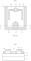
- Figure 4 is a plan view of a light emitting diode according to one exemplary embodiment
- Figure 5 is a cross-sectional view taken along line A-A of Figure 4 .
- a first conductive lower semiconductor layer 113 is formed on a substrate 111.
- the substrate 111 is not limited to a particular material, and may be a sapphire substrate.
- a second conductive upper semiconductor layer 117 is formed above the first conductive lower semiconductor layer 113.
- the upper semiconductor layer 117 is positioned within a region surrounded by edges of the lower semiconductor layer 113 to expose at least a portion of edge regions of the lower semiconductor layer 113.
- an active layer 115 is interposed between the lower semiconductor layer 113 and the upper semiconductor layer 117.
- the active layer 115 is positioned under the upper semiconductor layer 117 while exposing the at least a portion of the edge regions of the lower semiconductor layer 113.
- the lower semiconductor layer 113, active layer 115 and upper semiconductor layer 117 may be formed of, but not limited to, a GaN-based compound semiconductor material such as (B, Al, In, Ga)N.
- the active layer 115 is composed of elements determined to emit light at desired frequencies, for example, UV or blue light.
- the lower semiconductor layer 113 and the upper semiconductor layer 117 are formed of materials having a greater band gap than the active layer 115.
- the lower semiconductor layer 113 and/or the upper semiconductor layer 117 may have a single layer structure or a multilayer structure.
- the active layer 115 may have a single quantum well structure or a multi-quantum well structure.
- the light emitting diode may further include a buffer layer (not shown) between the substrate 111 and the lower semiconductor layer 113. The buffer layer is selected to relieve lattice mismatch between the substrate 111 and the lower semiconductor layer 113 formed thereon.
- These semiconductor layers 113, 115, 117 may be formed by metal organic chemical vapor deposition (MOCVD) or molecular beam epitaxy (MBE) and may be subjected to mesa-etching to expose regions of the lower semiconductor layer 113 via photolithography and etching.
- MOCVD metal organic chemical vapor deposition
- MBE molecular beam epitaxy
- mesa-etching may be performed to form an inclined mesa surface on the semiconductor layer.
- the mesa surface may have a degree of inclination in the range of 20-80 degrees, and preferably in the range of 30-60 degrees.
- the inclined mesa surface may enhance workability and reliability when forming a second insulation layer 140 of a DBR structure and an inclined extension part 122 of the first electrode described below.
- the inclined mesa surface increases a light emitting area.
- the insulation layer is formed on the upper semiconductor layer 117.
- the insulation layer may include a first insulation layer 119 and a second insulation layer 140.
- the first insulation layer 119 is formed on the entire upper surface of the upper semiconductor layer 117 and the inclined surface which is formed by mesa etching, and may be formed of, for example, SiO 2 , Si 3 N 4 , Nb 2 O 5 , TiO 2 , etc.
- the second insulation layer 140 may be formed on a selected region of the upper semiconductor layer 117 where the first electrode 121 is to be formed, and a selected region of the mesa surface where the inclined extension part 122 of the first electrode 121 is to be formed, the mesa surface being formed by the mesa etching.
- the second insulation layer 140 may be formed, for example, in a distributed Bragg reflector (DBR) structure by alternately stacking materials, which have a great difference in index of refraction therebetween.
- DBR distributed Bragg reflector
- the DBR layer is used to provide high reflectivity to a variety of light emitting devices, which have a light emitting function, a light detection function, a light conversion function, etc.
- the DBR layer may be formed by alternately stacking two kinds of media having different indices of refraction to reflect light based on the difference between the indices of refraction.
- the second insulation layer 140 is formed by alternately stacking two or more insulation layers having different indices of refraction, for example, SiO 2 , Si 3 N 4 , Nb 2 O 5 , or TiO 2 .
- the second insulation layer 140 may be formed by alternately stacking, for example, multiple layers of SiO 2 and TiO 2 or multiple layers of SiO 2 and Si 3 N 4 , followed by etching the stacked insulation layers in a predetermined pattern using photolithography.
- the insulation layers are stacked such that insulation layers comprising a Si compound, that is, SiO 2 , become the outermost layers. TiO 2 may suffer from deformation when subjected to thermal stress. If an insulation layer of TiO 2 is positioned at the outermost side when forming the second insulation layer 140 by alternately stacking SiO 2 and TiO 2 , cracking of the second insulation layer 140 may occur after deposition of the second insulation layer 140. However, when stacking multiple layers of SiO 2 layers and TiO 2 layers by first stacking a SiO 2 layer exhibiting less response to thermal stress at the outermost side and then stacking a TiO 2 layer on the SiO 2 layer, the second insulation layer 240 exhibits thermal stability, thereby preventing cracking of the second insulation layer 140 after deposition thereof.
- the second insulation layer 140 include a SiO 2 insulation layer as the outermost layer, which is finally deposited. This structure may guarantee reliability of the second insulation layer 140. Since the second insulation layer 140 is formed by alternately stacking the insulation layers having different indices of refraction one above another, the second insulation layer 140 may have functions of the DBR. Accordingly, when light emitted from the active layer 117 is directed towards the first electrode 121, the second insulation layer 140 may reflect the light, thereby effectively preventing the light emitted from the active layer 117 from being absorbed or blocked by the first electrode 121.
- a DBR layer 111b may be formed on a PSS region 111a of the substrate 111.
- an insulation layer having the DBR structure is also formed under the second electrode 131 excluding a portion contacting the upper semiconductor layer 117, as well as the second insulation layer 140 of the DBR structure formed under the first electrode 121.
- an insulation layer of the DBR structure is also formed on an exposed portion of the lower semiconductor layer 113 in order to improve emission of light reflected by the second insulation layer 140 under the first electrode 121 or on the mesa surface.
- a DBR layer 111c may be formed on a bottom side of the substrate 111, as shown in Figure 6 .
- the first electrode 121 is formed in a first region on the upper semiconductor layer 117, with the first and second insulation layers 119, 140 interposed between the first electrode 121 and the upper semiconductor layer 117.
- An inclined extension part 122 and a lower extension part 123 of the first electrode extend from the first electrode 121 to an edge region of the exposed lower semiconductor layer 113 and are formed along a first side of the substrate.
- the first electrode 121, the inclined extension part 122 and the lower extension part 123 of the first electrode may be formed of the same material using the same process.
- the lower semiconductor layer is an N-type semiconductor layer
- the first electrode 121, the inclined extension part 122 and the lower extension part 123 of the first electrode may be formed of Ti/Al using a lift-off process.
- the second electrode 131 is formed in a second region on the upper semiconductor layer 117.
- the second electrode 131 is positioned near a corner between a second side adjacent the first side and a third side adjacent the second side on the upper semiconductor layer 117.
- a transparent electrode layer may be formed on the upper semiconductor layer 117 before forming the first insulation layer 119.
- the transparent electrode layer is formed of indium tin oxide (ITO) or Ni/Au and has transparency.
- the transparent electrode layer may lower contact resistance through ohmic contact with the upper semiconductor layer 117.
- the second electrode 131 has neither transparency nor forms an ohmic contact with the upper semiconductor layer 117. A portion of the second electrode 131 is formed to contact with the upper semiconductor layer 117, and the other portion of the second electrode 131 is formed to contact with the transparent electrode layer. Consequently, the second electrode 131 is configured to form a direct contact with the upper semiconductor layer 117, thereby preventing electric current from flowing under the second electrode 131.
- the light is not generated in the domain of the active layer which is placed under the second electrode 131, but generated in the domain of the active layer which is placed under the transparent electrode layer .
- this structure it is possible to minimize the light emitted from the active layer being absorbed and lost by the second electrode 131.
- a first extension part 132 of the second electrode extends from the second electrode 131 on the upper semiconductor layer 117 to be formed adjacent the second side.
- a second extension part 133 of the second electrode extends from the second electrode 131 on the upper semiconductor layer 117 to be formed adjacent the third side.
- the second electrode 131 and the first and second extension parts 132, 133 of the second electrode may be formed of the same material using the same process.
- the second insulation layer 140 of the DBR structure formed under the first electrode 121 allows light to be effectively emitted to the outside instead of being absorbed or blocked by the first electrode 121.
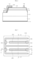
- Figure 7 is a plan view of a light emitting diode according to a further exemplary embodiment
- Figure 8 is a cross-sectional view taken along line B-B' of Figure 7
- Figure 9 is a cross-sectional view taken along line C-C' of Figure 7 .
- FIG. 7 to 9 is different from the embodiment of Figure 4 and Figure 5 in terms of the number, positions and shapes of first and second electrodes, and the shapes of extension parts of the first and second electrodes.
- first electrodes 221, 224 are formed to face second electrodes 231, 234 on an upper semiconductor layer 217.
- Each of extension parts 223, 225 of the first electrodes is positioned between extension parts 232, 233 or extension parts 233, 235 of the second electrodes to face each other.
- a first conductive lower semiconductor layer 213 is formed on a substrate 211.
- the substrate 211 is not limited to a particular material, and may be a sapphire substrate.
- a second conductive upper semiconductor layer 217 is formed above the first conductive lower semiconductor layer 213.
- the upper semiconductor layer 217 is positioned within a region surrounded by edges of the lower semiconductor layer 213 to expose at least a portion of edge regions of the lower semiconductor layer 213.
- an active layer 215 is interposed between the lower semiconductor layer 213 and the upper semiconductor layer 217.
- the active layer 215 is positioned under the upper semiconductor layer 217 while exposing the at least a portion of the edge regions of the lower semiconductor layer 213.
- the lower semiconductor layer 213, active layer 215 and upper semiconductor layer 217 may be formed of, but not limited to, a GaN-based compound semiconductor material such as (B, Al, In, Ga)N.
- the active layer 215 is composed of elements determined to emit light at desired frequencies, for example, UV or blue light.
- the lower semiconductor layer 213 and the upper semiconductor layer 217 are formed of materials having a greater band gap than the active layer 215.
- the lower semiconductor layer 213 and/or the upper semiconductor layer 217 may have a single layer structure or a multilayer structure.
- the active layer 215 may have a single quantum well structure or a multi-quantum well structure.
- the light emitting diode may further include a buffer layer (not shown) between the substrate 211 and the lower semiconductor layer 213. The buffer layer is selected to relieve lattice mismatch between the substrate 211 and the lower semiconductor layer 213 formed thereon.
- These semiconductor layers 213, 215, 217 may be formed by MOCVD or MBE and may be subjected to mesa-etching to expose regions of the lower semiconductor layer 213 via photolithography and etching.
- mesa-etching may be performed to form an inclined mesa surface on the semiconductor layer.
- the mesa surface may have a degree of inclination in the range of 20-80 degrees, and preferably in the range of 30-60 degrees.
- the inclined mesa surface may enhance workability and reliability when forming a DBR layer 240 and an inclined extension part 222 of the first electrode described below.
- the inclined mesa surface provides an effect of increasing a light emitting area.
- the insulation layer is formed on the upper semiconductor layer 217.
- the insulation layer may include a first insulation layer 219 and a second insulation layer 240.
- the first insulation layer 219 is formed on entire upper surface of the upper semiconductor layer 217 and the inclined mesa surface which is formed by mesa etching, and may be formed of for example, SiO 2 , Si 3 N 4 , Nb 2 O 5 , TiO 2 , etc.
- the second insulation layer 240 may be formed on a selected region of the upper semiconductor layer 217 where the first electrodes 221, 224 is to be formed, and a selected region of the mesa surface where the inclined extension parts 222, 225 of the first electrodes 221, 224 are to be formed, the mesa surface being formed by the mesa etching.
- the second insulation layer 240 may be formed, for example, in a DBR structure by alternately stacking materials, which have a great difference in index of refraction therebetween.
- the DBR layer is used to provide high reflectivity to a variety of light emitting devices, which have a light emitting function, a light detection function, a light conversion function, etc.
- the DBR layer may be formed by alternately stacking two kinds of media having different indices of refraction to reflect light based on the difference between the indices of refraction.
- the second insulation layer 240 is formed by alternately stacking two or more insulation layers having different indices of refraction, for example, SiO 2 , Si 3 N 4 , Nb 2 O 5 , or TiO 2 .
- the second insulation layer 240 may be formed by alternately stacking, for example, multiple layers of SiO 2 and TiO 2 or multiple layers of SiO 2 and Si 3 N 4 , followed by etching a predetermined pattern into the stacked insulation layers using photolithography.
- the insulation layers are stacked such that insulation layers comprising a Si compound, that is, SiO 2 , become the outermost layers.
- TiO 2 may suffer from deformation when subjected to thermal stress. If an insulation layer of TiO 2 is positioned at the outermost side when forming the second insulation layer 240 by alternately stacking SiO 2 and TiO 2 , cracking of the second insulation layer 240 may occur after deposition of the second insulation layer 240.
- the second insulation layer 240 when stacking multiple layers of SiO 2 layers and TiO 2 layers by first stacking a SiO 2 layer exhibiting less response to thermal stress at the outermost side and then stacking a TiO 2 layer on the SiO 2 layer, the second insulation layer 240 exhibits thermal stability, thereby preventing cracking of the second insulation layer 240 after deposition thereof. Likewise, it is desirable that the second insulation layer 240 include a SiO 2 insulation layer as the outermost layer, which is finally deposited. This structure may guarantee reliability of the second insulation layer 240.
- the second insulation layer 240 may have functions of the DBR. Accordingly, when light emitted from the active layer 217 is directed towards the first electrodes 221, 224, the second insulation layer 240 may reflect the light, thereby effectively preventing the light emitted from the active layer 217 from being absorbed or blocked by the first electrodes 221, 224.
- a DBR layer 211b may be formed on a PSS region 211a on the substrate 211.
- an insulation layer having the DBR structure is also formed under the second electrodes 231, 234 excluding a portion contacting the upper semiconductor layer 217, as well as the second insulation layer 240 of the DBR structure formed under the first electrodes 221, 224.
- an insulation layer of the DBR structure is also formed on an exposed portion of the lower semiconductor layer 213 in order to improve emission of light reflected by the second insulation layer 240 under the first electrodes 221, 224 or on the mesa surface.
- a DBR layer 211c may be formed on a bottom side of the substrate 211, as shown in Figure 10 .
- the first electrodes 221, 224 are formed in a first region on the upper semiconductor layer 217, with the first and second insulation layers 219, 240 interposed between the first electrodes and the upper semiconductor layer.
- the extension parts 223, 225 of the first electrodes extend from the first electrodes 221, 224 to an edge region of the exposed lower semiconductor layer 213.
- the first electrodes 221, 224 and the extension parts 223, 225 of the first electrodes may be formed of the same material using the same process. For example, if the lower semiconductor layer is an N-type semiconductor layer, the first electrodes 221, 224 and the extension parts 223, 225 of the first electrodes may be formed of Ti/Al using a lift-off process.
- the second electrodes 231, 234 are formed in a second region on the upper semiconductor layer 217.
- the second electrodes 231, 234 are positioned near an edge of a second side facing a first side on the upper semiconductor layer 217 to be separated a predetermined distance from each other.
- a transparent electrode layer (not shown) may be formed on the upper semiconductor layer 217 before forming the first insulation layer 219.
- the transparent electrode layer is formed of indium tin oxide (ITO) or Ni/Au and has transparency.
- the transparent electrode layer may lower contact resistance through ohmic contact with the upper semiconductor layer 217.
- the second electrodes 231, 234 have neither transparency nor form an ohmic contact with the upper semiconductor layer 217. A portion of the second electrodes 231, 234 are formed to contact with the upper semiconductor layer 217, and the other portion of the second electrodes 231, 234 are formed to contact with the transparent electrode layer.
- the second electrodes 231, 234 are configured to form a direct contact with the upper semiconductor layer 217, thereby preventing electric current from flowing under the second electrodes 231, 234. Therefore, the light is not generated in the domain of the active layer which is placed under the second electrodes 231, 234, but generated in the domain of the active layer which is placed under the transparent electrode layer . With this structure, it is possible to minimize the light emitted from the active layer being absorbed and lost by the second electrodes 231, 234.
- a first extension part 232 of the second electrode extends from the second electrode 231 on the upper semiconductor layer 217 to be formed adjacent the third side.
- a second extension part 233 of the second electrode extends along a central line of the substrate from an intermediate portion between the second electrodes 231, 234.
- a third extension part 233 of the second electrode extends from the second electrode 234 on the upper semiconductor layer 217 to be formed adjacent a fourth side facing the third side.
- the second electrodes 231, 234 and the first, second and third extension parts 232, 233, 235 of the second electrode may be formed of the same material using the same process.
- the first electrodes 221, 224 are formed above the upper semiconductor layer 217, with the first and second insulation layers 219, 240 interposed between the first electrodes and the upper semiconductor layer 217, and the active layer 215 remains unetched.
- the light emitting diode according to the embodiment provides an effective solution to the problem of the related art in which the light emitting area is reduced due to the formation of the electrode.
- the second insulation layer 240 of the DBR structure formed under the first electrodes 221, 224 allows light to be effectively emitted to the outside instead of being absorbed or blocked by the first electrodes 221, 224.
- an electrode and an extension part for supplying current to a lower semiconductor layer are formed above an upper semiconductor layer with an insulation layer interposed between the electrode and the upper semiconductor layer. Consequently, an area of the semiconductor layer removed by mesa-etching for forming the electrode and the extension part is reduced, thereby preventing a reduction in light emitting area.
- the insulation layer of the DBR structure is formed by alternately stacking two or more insulation layers having different indices of refraction such that the outermost insulation layers are formed of SiO 2 , to enhance reliability of the DBR structure.
- this feature may also be applied to all insulation layers set forth herein.
Landscapes
- Engineering & Computer Science (AREA)
- Manufacturing & Machinery (AREA)
- Computer Hardware Design (AREA)
- Microelectronics & Electronic Packaging (AREA)
- Power Engineering (AREA)
- Led Devices (AREA)
Priority Applications (1)
| Application Number | Priority Date | Filing Date | Title |
|---|---|---|---|
| EP23168470.5A EP4220743A3 (en) | 2009-12-28 | 2010-11-23 | Light emitting diode |
Applications Claiming Priority (2)
| Application Number | Priority Date | Filing Date | Title |
|---|---|---|---|
| KR1020090131693A KR101654340B1 (ko) | 2009-12-28 | 2009-12-28 | 발광 다이오드 |
| EP10192249.0A EP2339654B1 (en) | 2009-12-28 | 2010-11-23 | Light emitting diode |
Related Parent Applications (1)
| Application Number | Title | Priority Date | Filing Date |
|---|---|---|---|
| EP10192249.0A Division EP2339654B1 (en) | 2009-12-28 | 2010-11-23 | Light emitting diode |
Related Child Applications (1)
| Application Number | Title | Priority Date | Filing Date |
|---|---|---|---|
| EP23168470.5A Division EP4220743A3 (en) | 2009-12-28 | 2010-11-23 | Light emitting diode |
Publications (2)
| Publication Number | Publication Date |
|---|---|
| EP3758076A1 EP3758076A1 (en) | 2020-12-30 |
| EP3758076B1 true EP3758076B1 (en) | 2023-04-19 |
Family
ID=43828431
Family Applications (3)
| Application Number | Title | Priority Date | Filing Date |
|---|---|---|---|
| EP23168470.5A Pending EP4220743A3 (en) | 2009-12-28 | 2010-11-23 | Light emitting diode |
| EP10192249.0A Active EP2339654B1 (en) | 2009-12-28 | 2010-11-23 | Light emitting diode |
| EP20190306.9A Active EP3758076B1 (en) | 2009-12-28 | 2010-11-23 | Light emitting diode |
Family Applications Before (2)
| Application Number | Title | Priority Date | Filing Date |
|---|---|---|---|
| EP23168470.5A Pending EP4220743A3 (en) | 2009-12-28 | 2010-11-23 | Light emitting diode |
| EP10192249.0A Active EP2339654B1 (en) | 2009-12-28 | 2010-11-23 | Light emitting diode |
Country Status (7)
| Country | Link |
|---|---|
| US (2) | US8946744B2 (pl) |
| EP (3) | EP4220743A3 (pl) |
| JP (1) | JP5639856B2 (pl) |
| KR (1) | KR101654340B1 (pl) |
| CN (2) | CN102110754B (pl) |
| PL (1) | PL3758076T3 (pl) |
| TW (1) | TWI464914B (pl) |
Families Citing this family (53)
| Publication number | Priority date | Publication date | Assignee | Title |
|---|---|---|---|---|
| US9236532B2 (en) * | 2009-12-14 | 2016-01-12 | Seoul Viosys Co., Ltd. | Light emitting diode having electrode pads |
| KR101039999B1 (ko) * | 2010-02-08 | 2011-06-09 | 엘지이노텍 주식회사 | 반도체 발광소자 및 그 제조방법 |
| KR101194844B1 (ko) * | 2010-11-15 | 2012-10-25 | 삼성전자주식회사 | 발광소자 및 그 제조방법 |
| JP5652234B2 (ja) * | 2011-02-07 | 2015-01-14 | 日亜化学工業株式会社 | 半導体発光素子 |
| JP5776203B2 (ja) * | 2011-02-14 | 2015-09-09 | 日亜化学工業株式会社 | 発光素子 |
| CN108807626B (zh) * | 2011-09-15 | 2020-02-21 | 晶元光电股份有限公司 | 发光元件 |
| JP5961359B2 (ja) * | 2011-09-20 | 2016-08-02 | 昭和電工株式会社 | 発光ダイオード及びその製造方法 |
| WO2013051326A1 (ja) * | 2011-10-05 | 2013-04-11 | シャープ株式会社 | 窒化物半導体発光素子、及び窒化物半導体発光素子の製造方法 |
| KR101981119B1 (ko) * | 2011-11-25 | 2019-05-22 | 엘지이노텍 주식회사 | 자외선 반도체 발광 소자 |
| JP2013145867A (ja) * | 2011-12-15 | 2013-07-25 | Hitachi Cable Ltd | 窒化物半導体テンプレート及び発光ダイオード |
| KR101883842B1 (ko) * | 2011-12-26 | 2018-08-01 | 엘지이노텍 주식회사 | 발광소자 및 이를 포함하는 조명시스템 |
| TWI479694B (zh) | 2012-01-11 | 2015-04-01 | Formosa Epitaxy Inc | Light emitting diode wafers |
| US9076923B2 (en) * | 2012-02-13 | 2015-07-07 | Epistar Corporation | Light-emitting device manufacturing method |
| TWI572054B (zh) * | 2012-03-16 | 2017-02-21 | 晶元光電股份有限公司 | 高亮度發光二極體結構與其製造方法 |
| KR101293495B1 (ko) * | 2012-03-20 | 2013-08-06 | 주식회사 세미콘라이트 | 반도체 발광소자 |
| US8748928B2 (en) | 2012-05-17 | 2014-06-10 | High Power Opto, Inc. | Continuous reflection curved mirror structure of a vertical light-emitting diode |
| US8546831B1 (en) * | 2012-05-17 | 2013-10-01 | High Power Opto Inc. | Reflection convex mirror structure of a vertical light-emitting diode |
| US8816379B2 (en) | 2012-05-17 | 2014-08-26 | High Power Opto, Inc. | Reflection curved mirror structure of a vertical light-emitting diode |
| US9496458B2 (en) * | 2012-06-08 | 2016-11-15 | Cree, Inc. | Semiconductor light emitting diodes with crack-tolerant barrier structures and methods of fabricating the same |
| JP2013258174A (ja) * | 2012-06-11 | 2013-12-26 | Nichia Chem Ind Ltd | 半導体発光素子 |
| CN103489980A (zh) * | 2012-06-12 | 2014-01-01 | 群康科技(深圳)有限公司 | 一种发光元件及其制作方法 |
| WO2014038794A1 (ko) * | 2012-09-07 | 2014-03-13 | 서울바이오시스 주식회사 | 웨이퍼 레벨의 발광 다이오드 어레이 |
| KR102013363B1 (ko) * | 2012-11-09 | 2019-08-22 | 서울바이오시스 주식회사 | 발광 소자 및 그것을 제조하는 방법 |
| CN110600593B (zh) * | 2012-12-06 | 2023-01-03 | 首尔伟傲世有限公司 | 发光二极管 |
| CN102945906A (zh) * | 2012-12-06 | 2013-02-27 | 上海顿格电子贸易有限公司 | 水平结构的led芯片 |
| JP6102677B2 (ja) | 2012-12-28 | 2017-03-29 | 日亜化学工業株式会社 | 発光素子 |
| KR102145891B1 (ko) * | 2013-04-23 | 2020-08-20 | 루미리즈 홀딩 비.브이. | 발광 장치를 위한 측면 상호접속부 |
| TWI604633B (zh) * | 2013-11-05 | 2017-11-01 | 晶元光電股份有限公司 | 發光元件 |
| CN104638084B (zh) * | 2013-11-11 | 2019-07-02 | 晶元光电股份有限公司 | 发光元件 |
| US9666779B2 (en) * | 2013-11-25 | 2017-05-30 | Yangzhou Zhongke Semiconductor Lighting Co., Ltd. | Semiconductor light emitting diode chip with current extension layer and graphical current extension layers |
| JP6458463B2 (ja) | 2013-12-09 | 2019-01-30 | 日亜化学工業株式会社 | 発光素子 |
| JP2015207754A (ja) * | 2013-12-13 | 2015-11-19 | 日亜化学工業株式会社 | 発光装置 |
| WO2015145899A1 (ja) * | 2014-03-24 | 2015-10-01 | シャープ株式会社 | 窒化物半導体発光素子 |
| KR102357289B1 (ko) * | 2014-07-01 | 2022-02-03 | 서울바이오시스 주식회사 | 발광 소자 |
| CN104269471A (zh) * | 2014-09-28 | 2015-01-07 | 映瑞光电科技(上海)有限公司 | 全角度侧壁反射电极的led芯片及其制作方法 |
| JP2016100510A (ja) * | 2014-11-25 | 2016-05-30 | 泰谷光電科技股▲ふん▼有限公司 | 電流拡散構成を有する発光ダイオード |
| KR102322842B1 (ko) * | 2014-12-26 | 2021-11-08 | 엘지이노텍 주식회사 | 발광 소자 어레이 |
| US9905729B2 (en) * | 2015-03-27 | 2018-02-27 | Seoul Viosys Co., Ltd. | Light emitting diode |
| WO2016177333A1 (zh) * | 2015-05-05 | 2016-11-10 | 湘能华磊光电股份有限公司 | Iii族半导体发光器件倒装结构的制作方法 |
| CN105720156B (zh) * | 2016-02-03 | 2018-07-31 | 华灿光电(苏州)有限公司 | 一种发光二极管及其制作方法 |
| JP6668863B2 (ja) * | 2016-03-22 | 2020-03-18 | 日亜化学工業株式会社 | 発光素子 |
| CN105957928B (zh) * | 2016-05-31 | 2018-10-09 | 华灿光电股份有限公司 | 一种谐振腔发光二极管及其制造方法 |
| CN106129206B (zh) * | 2016-07-29 | 2019-02-26 | 天津三安光电有限公司 | 具有全镜面结构的发光二极管及其制作方法 |
| DE102017111123A1 (de) * | 2017-05-22 | 2018-11-22 | Osram Opto Semiconductors Gmbh | Optoelektronischer Halbleiterchip und Verfahren zur Herstellung eines optoelektronischen Halbleiterchips |
| US10892297B2 (en) * | 2017-11-27 | 2021-01-12 | Seoul Viosys Co., Ltd. | Light emitting diode (LED) stack for a display |
| JP7079106B2 (ja) * | 2018-01-24 | 2022-06-01 | シャープ株式会社 | 画像表示素子、及び画像表示素子の製造方法 |
| TWI661574B (zh) * | 2018-06-06 | 2019-06-01 | 友達光電股份有限公司 | 微型發光二極體顯示器、微型發光二極體元件及其製作方法 |
| CN109244207A (zh) * | 2018-08-30 | 2019-01-18 | 佛山市国星半导体技术有限公司 | 一种led芯片及其制作方法 |
| CN109088309B (zh) * | 2018-10-16 | 2024-01-26 | 厦门乾照半导体科技有限公司 | 一种高频垂直腔面发射激光器芯片及其制备方法 |
| KR102624112B1 (ko) * | 2018-10-23 | 2024-01-12 | 서울바이오시스 주식회사 | 플립칩형 발광 다이오드 칩 |
| CN111463329B (zh) * | 2019-01-18 | 2021-09-17 | 北京北方华创微电子装备有限公司 | 一种led芯片及其制作方法 |
| CN112117358B (zh) * | 2020-09-22 | 2021-07-16 | 宁波天炬光电科技有限公司 | 单芯片大功率led芯片结构 |
| CN112467006B (zh) * | 2020-11-27 | 2023-05-16 | 錼创显示科技股份有限公司 | 微型发光二极管结构与使用其的微型发光二极管显示设备 |
Family Cites Families (30)
| Publication number | Priority date | Publication date | Assignee | Title |
|---|---|---|---|---|
| TW365071B (en) * | 1996-09-09 | 1999-07-21 | Toshiba Corp | Semiconductor light emitting diode and method for manufacturing the same |
| JP3346735B2 (ja) * | 1998-03-03 | 2002-11-18 | 日亜化学工業株式会社 | 窒化物半導体発光素子及びその製造方法 |
| GB9807692D0 (en) * | 1998-04-14 | 1998-06-10 | Univ Strathclyde | Optival devices |
| US6504180B1 (en) * | 1998-07-28 | 2003-01-07 | Imec Vzw And Vrije Universiteit | Method of manufacturing surface textured high-efficiency radiating devices and devices obtained therefrom |
| JP3896704B2 (ja) * | 1998-10-07 | 2007-03-22 | 松下電器産業株式会社 | GaN系化合物半導体発光素子 |
| JP3849506B2 (ja) * | 2000-11-28 | 2006-11-22 | 日亜化学工業株式会社 | 窒化物半導体成長基板および保護膜を用いた窒化物半導体基板の成長方法 |
| US6630689B2 (en) * | 2001-05-09 | 2003-10-07 | Lumileds Lighting, U.S. Llc | Semiconductor LED flip-chip with high reflectivity dielectric coating on the mesa |
| AU2003252359A1 (en) * | 2002-08-01 | 2004-02-23 | Nichia Corporation | Semiconductor light-emitting device, method for manufacturing same and light-emitting apparatus using same |
| ES2356606T3 (es) * | 2003-08-08 | 2011-04-11 | Kang, Sang-Kyu | Microdiodo emisor de luz de nitruro con alto brillo y procedimiento de fabricación del mismo. |
| JP4273928B2 (ja) * | 2003-10-30 | 2009-06-03 | 豊田合成株式会社 | Iii−v族窒化物半導体素子 |
| WO2005081319A1 (de) * | 2004-02-20 | 2005-09-01 | Osram Opto Semiconductors Gmbh | Optoelektronisches bauelement, vorrichtung mit einer mehrzahl optoelektronischer bauelemente und verfahren zur herstellung eines optoelektronischen bauelements |
| CN100524855C (zh) * | 2004-03-31 | 2009-08-05 | 日亚化学工业株式会社 | 氮化物半导体发光元件 |
| JP2006012916A (ja) * | 2004-06-22 | 2006-01-12 | Toyoda Gosei Co Ltd | 発光素子 |
| JP2006128450A (ja) * | 2004-10-29 | 2006-05-18 | Toyoda Gosei Co Ltd | Iii族窒化物半導体発光素子 |
| TWI253188B (en) * | 2004-11-19 | 2006-04-11 | Epistar Corp | Method of forming light emitting diode array |
| TWI244228B (en) * | 2005-02-03 | 2005-11-21 | United Epitaxy Co Ltd | Light emitting device and manufacture method thereof |
| US7737455B2 (en) * | 2006-05-19 | 2010-06-15 | Bridgelux, Inc. | Electrode structures for LEDs with increased active area |
| US7573074B2 (en) * | 2006-05-19 | 2009-08-11 | Bridgelux, Inc. | LED electrode |
| TW200828624A (en) * | 2006-12-27 | 2008-07-01 | Epistar Corp | Light-emitting diode and method for manufacturing the same |
| JP4305554B2 (ja) * | 2007-02-28 | 2009-07-29 | ソニー株式会社 | 半導体レーザの製造方法 |
| TWI343663B (en) * | 2007-05-15 | 2011-06-11 | Epistar Corp | Light emitting diode device and manufacturing method therof |
| KR100941766B1 (ko) * | 2007-08-08 | 2010-02-11 | 한국광기술원 | 패드 재배열을 이용한 반도체 발광 다이오드 및 그의제조방법 |
| KR101393353B1 (ko) * | 2007-10-29 | 2014-05-13 | 서울바이오시스 주식회사 | 발광다이오드 |
| TWI370558B (en) * | 2007-11-07 | 2012-08-11 | Ind Tech Res Inst | Light emitting diode and process for fabricating the same |
| KR101354981B1 (ko) * | 2007-11-14 | 2014-01-27 | 삼성전자주식회사 | 질화물 반도체 발광 다이오드 |
| US8368100B2 (en) * | 2007-11-14 | 2013-02-05 | Cree, Inc. | Semiconductor light emitting diodes having reflective structures and methods of fabricating same |
| JP4974867B2 (ja) * | 2007-12-12 | 2012-07-11 | 昭和電工株式会社 | 発光ダイオード及びその製造方法 |
| CN101257072B (zh) * | 2007-12-26 | 2010-12-15 | 厦门市三安光电科技有限公司 | 一种立体式空间分布电极的发光二极管及其制造方法 |
| KR101457204B1 (ko) * | 2008-02-01 | 2014-11-03 | 서울바이오시스 주식회사 | 발광 다이오드 및 그 제조방법 |
| WO2009125953A2 (ko) * | 2008-04-06 | 2009-10-15 | Song June O | 발광 소자 |
-
2009
- 2009-12-28 KR KR1020090131693A patent/KR101654340B1/ko active Application Filing
-
2010
- 2010-11-18 JP JP2010257901A patent/JP5639856B2/ja active Active
- 2010-11-18 TW TW099139730A patent/TWI464914B/zh active
- 2010-11-23 EP EP23168470.5A patent/EP4220743A3/en active Pending
- 2010-11-23 PL PL20190306.9T patent/PL3758076T3/pl unknown
- 2010-11-23 EP EP10192249.0A patent/EP2339654B1/en active Active
- 2010-11-23 EP EP20190306.9A patent/EP3758076B1/en active Active
- 2010-12-21 US US12/974,605 patent/US8946744B2/en active Active
- 2010-12-28 CN CN201010623389.7A patent/CN102110754B/zh active Active
- 2010-12-28 CN CN201410374382.4A patent/CN104241488A/zh active Pending
-
2014
- 2014-12-05 US US14/561,957 patent/US20150091038A1/en not_active Abandoned
Also Published As
| Publication number | Publication date |
|---|---|
| CN102110754B (zh) | 2014-09-03 |
| PL3758076T3 (pl) | 2023-08-28 |
| JP2011139037A (ja) | 2011-07-14 |
| CN104241488A (zh) | 2014-12-24 |
| EP4220743A2 (en) | 2023-08-02 |
| KR20110075279A (ko) | 2011-07-06 |
| EP4220743A3 (en) | 2023-11-29 |
| US20110156070A1 (en) | 2011-06-30 |
| EP3758076A1 (en) | 2020-12-30 |
| TWI464914B (zh) | 2014-12-11 |
| US8946744B2 (en) | 2015-02-03 |
| EP2339654A3 (en) | 2013-02-06 |
| TW201133943A (en) | 2011-10-01 |
| JP5639856B2 (ja) | 2014-12-10 |
| CN102110754A (zh) | 2011-06-29 |
| EP2339654B1 (en) | 2020-08-12 |
| EP2339654A2 (en) | 2011-06-29 |
| US20150091038A1 (en) | 2015-04-02 |
| KR101654340B1 (ko) | 2016-09-06 |
Similar Documents
| Publication | Publication Date | Title |
|---|---|---|
| EP3758076B1 (en) | Light emitting diode | |
| US9397264B2 (en) | Light emitting diode chip having electrode pad | |
| US10608141B2 (en) | Light emitting diode chip having electrode pad | |
| US9269871B2 (en) | Light emitting diode | |
| US8541806B2 (en) | Light emitting diode having electrode pads | |
| JP2013533644A (ja) | 改善された光抽出効率を有する発光ダイオード | |
| JP2009054688A (ja) | 発光素子 | |
| US10734550B2 (en) | Semiconductor device | |
| KR101272705B1 (ko) | 균일한 전류밀도 특성을 갖는 발광 다이오드 | |
| KR20150107400A (ko) | 발광 다이오드 | |
| KR101654342B1 (ko) | 고효율 발광 다이오드 | |
| KR100631970B1 (ko) | 플립칩용 질화물 반도체 발광소자 | |
| KR20170095675A (ko) | 발광 소자 | |
| KR100756842B1 (ko) | 광추출용 컬럼들을 갖는 발광 다이오드 및 그것을 제조하는방법 | |
| US20240113262A1 (en) | Light-emitting device, backlight unit and display apparatus having the same | |
| KR20230026248A (ko) | 발광소자 | |
| KR20160105369A (ko) | 발광 다이오드 | |
| KR101171360B1 (ko) | 발광 다이오드 | |
| KR102071035B1 (ko) | 발광 다이오드 및 그것을 제조하는 방법 | |
| KR20200010805A (ko) | 발광소자 |
Legal Events
| Date | Code | Title | Description |
|---|---|---|---|
| PUAI | Public reference made under article 153(3) epc to a published international application that has entered the european phase |
Free format text: ORIGINAL CODE: 0009012 |
|
| STAA | Information on the status of an ep patent application or granted ep patent |
Free format text: STATUS: THE APPLICATION HAS BEEN PUBLISHED |
|
| AC | Divisional application: reference to earlier application |
Ref document number: 2339654 Country of ref document: EP Kind code of ref document: P |
|
| AK | Designated contracting states |
Kind code of ref document: A1 Designated state(s): AL AT BE BG CH CY CZ DE DK EE ES FI FR GB GR HR HU IE IS IT LI LT LU LV MC MK MT NL NO PL PT RO RS SE SI SK SM TR |
|
| STAA | Information on the status of an ep patent application or granted ep patent |
Free format text: STATUS: REQUEST FOR EXAMINATION WAS MADE |
|
| 17P | Request for examination filed |
Effective date: 20210630 |
|
| RBV | Designated contracting states (corrected) |
Designated state(s): AL AT BE BG CH CY CZ DE DK EE ES FI FR GB GR HR HU IE IS IT LI LT LU LV MC MK MT NL NO PL PT RO RS SE SI SK SM TR |
|
| GRAP | Despatch of communication of intention to grant a patent |
Free format text: ORIGINAL CODE: EPIDOSNIGR1 |
|
| STAA | Information on the status of an ep patent application or granted ep patent |
Free format text: STATUS: GRANT OF PATENT IS INTENDED |
|
| INTG | Intention to grant announced |
Effective date: 20221129 |
|
| GRAS | Grant fee paid |
Free format text: ORIGINAL CODE: EPIDOSNIGR3 |
|
| GRAA | (expected) grant |
Free format text: ORIGINAL CODE: 0009210 |
|
| STAA | Information on the status of an ep patent application or granted ep patent |
Free format text: STATUS: THE PATENT HAS BEEN GRANTED |
|
| AC | Divisional application: reference to earlier application |
Ref document number: 2339654 Country of ref document: EP Kind code of ref document: P |
|
| AK | Designated contracting states |
Kind code of ref document: B1 Designated state(s): AL AT BE BG CH CY CZ DE DK EE ES FI FR GB GR HR HU IE IS IT LI LT LU LV MC MK MT NL NO PL PT RO RS SE SI SK SM TR |
|
| REG | Reference to a national code |
Ref country code: GB Ref legal event code: FG4D |
|
| REG | Reference to a national code |
Ref country code: CH Ref legal event code: EP |
|
| REG | Reference to a national code |
Ref country code: DE Ref legal event code: R096 Ref document number: 602010068768 Country of ref document: DE |
|
| REG | Reference to a national code |
Ref country code: IE Ref legal event code: FG4D |
|
| REG | Reference to a national code |
Ref country code: AT Ref legal event code: REF Ref document number: 1561851 Country of ref document: AT Kind code of ref document: T Effective date: 20230515 |
|
| REG | Reference to a national code |
Ref country code: NL Ref legal event code: FP |
|
| REG | Reference to a national code |
Ref country code: LT Ref legal event code: MG9D |
|
| REG | Reference to a national code |
Ref country code: AT Ref legal event code: MK05 Ref document number: 1561851 Country of ref document: AT Kind code of ref document: T Effective date: 20230419 |
|
| PG25 | Lapsed in a contracting state [announced via postgrant information from national office to epo] |
Ref country code: SE Free format text: LAPSE BECAUSE OF FAILURE TO SUBMIT A TRANSLATION OF THE DESCRIPTION OR TO PAY THE FEE WITHIN THE PRESCRIBED TIME-LIMIT Effective date: 20230419 Ref country code: PT Free format text: LAPSE BECAUSE OF FAILURE TO SUBMIT A TRANSLATION OF THE DESCRIPTION OR TO PAY THE FEE WITHIN THE PRESCRIBED TIME-LIMIT Effective date: 20230821 Ref country code: NO Free format text: LAPSE BECAUSE OF FAILURE TO SUBMIT A TRANSLATION OF THE DESCRIPTION OR TO PAY THE FEE WITHIN THE PRESCRIBED TIME-LIMIT Effective date: 20230719 Ref country code: ES Free format text: LAPSE BECAUSE OF FAILURE TO SUBMIT A TRANSLATION OF THE DESCRIPTION OR TO PAY THE FEE WITHIN THE PRESCRIBED TIME-LIMIT Effective date: 20230419 Ref country code: AT Free format text: LAPSE BECAUSE OF FAILURE TO SUBMIT A TRANSLATION OF THE DESCRIPTION OR TO PAY THE FEE WITHIN THE PRESCRIBED TIME-LIMIT Effective date: 20230419 |
|
| PGFP | Annual fee paid to national office [announced via postgrant information from national office to epo] |
Ref country code: TR Payment date: 20230922 Year of fee payment: 14 Ref country code: NL Payment date: 20230921 Year of fee payment: 14 Ref country code: GB Payment date: 20230920 Year of fee payment: 14 |
|
| PG25 | Lapsed in a contracting state [announced via postgrant information from national office to epo] |
Ref country code: RS Free format text: LAPSE BECAUSE OF FAILURE TO SUBMIT A TRANSLATION OF THE DESCRIPTION OR TO PAY THE FEE WITHIN THE PRESCRIBED TIME-LIMIT Effective date: 20230419 Ref country code: LV Free format text: LAPSE BECAUSE OF FAILURE TO SUBMIT A TRANSLATION OF THE DESCRIPTION OR TO PAY THE FEE WITHIN THE PRESCRIBED TIME-LIMIT Effective date: 20230419 Ref country code: LT Free format text: LAPSE BECAUSE OF FAILURE TO SUBMIT A TRANSLATION OF THE DESCRIPTION OR TO PAY THE FEE WITHIN THE PRESCRIBED TIME-LIMIT Effective date: 20230419 Ref country code: IS Free format text: LAPSE BECAUSE OF FAILURE TO SUBMIT A TRANSLATION OF THE DESCRIPTION OR TO PAY THE FEE WITHIN THE PRESCRIBED TIME-LIMIT Effective date: 20230819 Ref country code: HR Free format text: LAPSE BECAUSE OF FAILURE TO SUBMIT A TRANSLATION OF THE DESCRIPTION OR TO PAY THE FEE WITHIN THE PRESCRIBED TIME-LIMIT Effective date: 20230419 Ref country code: GR Free format text: LAPSE BECAUSE OF FAILURE TO SUBMIT A TRANSLATION OF THE DESCRIPTION OR TO PAY THE FEE WITHIN THE PRESCRIBED TIME-LIMIT Effective date: 20230720 |
|
| PGFP | Annual fee paid to national office [announced via postgrant information from national office to epo] |
Ref country code: PL Payment date: 20230926 Year of fee payment: 14 Ref country code: FR Payment date: 20230922 Year of fee payment: 14 |
|
| PG25 | Lapsed in a contracting state [announced via postgrant information from national office to epo] |
Ref country code: FI Free format text: LAPSE BECAUSE OF FAILURE TO SUBMIT A TRANSLATION OF THE DESCRIPTION OR TO PAY THE FEE WITHIN THE PRESCRIBED TIME-LIMIT Effective date: 20230419 |
|
| PG25 | Lapsed in a contracting state [announced via postgrant information from national office to epo] |
Ref country code: SK Free format text: LAPSE BECAUSE OF FAILURE TO SUBMIT A TRANSLATION OF THE DESCRIPTION OR TO PAY THE FEE WITHIN THE PRESCRIBED TIME-LIMIT Effective date: 20230419 |
|
| REG | Reference to a national code |
Ref country code: DE Ref legal event code: R097 Ref document number: 602010068768 Country of ref document: DE |
|
| PG25 | Lapsed in a contracting state [announced via postgrant information from national office to epo] |
Ref country code: SM Free format text: LAPSE BECAUSE OF FAILURE TO SUBMIT A TRANSLATION OF THE DESCRIPTION OR TO PAY THE FEE WITHIN THE PRESCRIBED TIME-LIMIT Effective date: 20230419 Ref country code: SK Free format text: LAPSE BECAUSE OF FAILURE TO SUBMIT A TRANSLATION OF THE DESCRIPTION OR TO PAY THE FEE WITHIN THE PRESCRIBED TIME-LIMIT Effective date: 20230419 Ref country code: RO Free format text: LAPSE BECAUSE OF FAILURE TO SUBMIT A TRANSLATION OF THE DESCRIPTION OR TO PAY THE FEE WITHIN THE PRESCRIBED TIME-LIMIT Effective date: 20230419 Ref country code: EE Free format text: LAPSE BECAUSE OF FAILURE TO SUBMIT A TRANSLATION OF THE DESCRIPTION OR TO PAY THE FEE WITHIN THE PRESCRIBED TIME-LIMIT Effective date: 20230419 Ref country code: DK Free format text: LAPSE BECAUSE OF FAILURE TO SUBMIT A TRANSLATION OF THE DESCRIPTION OR TO PAY THE FEE WITHIN THE PRESCRIBED TIME-LIMIT Effective date: 20230419 Ref country code: CZ Free format text: LAPSE BECAUSE OF FAILURE TO SUBMIT A TRANSLATION OF THE DESCRIPTION OR TO PAY THE FEE WITHIN THE PRESCRIBED TIME-LIMIT Effective date: 20230419 |
|
| PGFP | Annual fee paid to national office [announced via postgrant information from national office to epo] |
Ref country code: IT Payment date: 20230922 Year of fee payment: 14 Ref country code: DE Payment date: 20230920 Year of fee payment: 14 |
|
| PLBE | No opposition filed within time limit |
Free format text: ORIGINAL CODE: 0009261 |
|
| STAA | Information on the status of an ep patent application or granted ep patent |
Free format text: STATUS: NO OPPOSITION FILED WITHIN TIME LIMIT |
|
| 26N | No opposition filed |
Effective date: 20240122 |
|
| PG25 | Lapsed in a contracting state [announced via postgrant information from national office to epo] |
Ref country code: SI Free format text: LAPSE BECAUSE OF FAILURE TO SUBMIT A TRANSLATION OF THE DESCRIPTION OR TO PAY THE FEE WITHIN THE PRESCRIBED TIME-LIMIT Effective date: 20230419 |