EP3656020B1 - Antenne à constante diélectrique variable ayant une électrode de masse divisée - Google Patents
Antenne à constante diélectrique variable ayant une électrode de masse divisée Download PDFInfo
- Publication number
- EP3656020B1 EP3656020B1 EP18836169.5A EP18836169A EP3656020B1 EP 3656020 B1 EP3656020 B1 EP 3656020B1 EP 18836169 A EP18836169 A EP 18836169A EP 3656020 B1 EP3656020 B1 EP 3656020B1
- Authority
- EP
- European Patent Office
- Prior art keywords
- ground
- antenna
- signal
- conductive
- patch
- Prior art date
- Legal status (The legal status is an assumption and is not a legal conclusion. Google has not performed a legal analysis and makes no representation as to the accuracy of the status listed.)
- Active
Links
- 230000004913 activation Effects 0.000 claims description 24
- 230000008878 coupling Effects 0.000 claims description 22
- 238000010168 coupling process Methods 0.000 claims description 22
- 238000005859 coupling reaction Methods 0.000 claims description 22
- 239000000758 substrate Substances 0.000 claims description 10
- 239000000463 material Substances 0.000 description 22
- 125000006850 spacer group Chemical group 0.000 description 16
- 239000011230 binding agent Substances 0.000 description 12
- 230000005540 biological transmission Effects 0.000 description 10
- 230000008859 change Effects 0.000 description 10
- 239000004020 conductor Substances 0.000 description 9
- 239000012212 insulator Substances 0.000 description 7
- 230000010287 polarization Effects 0.000 description 7
- 239000011521 glass Substances 0.000 description 6
- 238000004519 manufacturing process Methods 0.000 description 6
- 238000000034 method Methods 0.000 description 6
- 239000011248 coating agent Substances 0.000 description 5
- 238000000576 coating method Methods 0.000 description 5
- 239000004973 liquid crystal related substance Substances 0.000 description 5
- RYGMFSIKBFXOCR-UHFFFAOYSA-N Copper Chemical compound [Cu] RYGMFSIKBFXOCR-UHFFFAOYSA-N 0.000 description 4
- 229910052802 copper Inorganic materials 0.000 description 4
- 239000010949 copper Substances 0.000 description 4
- 239000011324 bead Substances 0.000 description 3
- 230000008901 benefit Effects 0.000 description 3
- 238000000926 separation method Methods 0.000 description 3
- 238000004544 sputter deposition Methods 0.000 description 3
- 239000004988 Nematic liquid crystal Substances 0.000 description 2
- 239000003990 capacitor Substances 0.000 description 2
- 238000010276 construction Methods 0.000 description 2
- 239000003989 dielectric material Substances 0.000 description 2
- -1 e.g. Substances 0.000 description 2
- 238000005530 etching Methods 0.000 description 2
- 238000007667 floating Methods 0.000 description 2
- 238000002955 isolation Methods 0.000 description 2
- 229920001343 polytetrafluoroethylene Polymers 0.000 description 2
- 239000004810 polytetrafluoroethylene Substances 0.000 description 2
- 230000005855 radiation Effects 0.000 description 2
- 241001674808 Biastes Species 0.000 description 1
- 239000004593 Epoxy Substances 0.000 description 1
- 239000004642 Polyimide Substances 0.000 description 1
- 239000004809 Teflon Substances 0.000 description 1
- 229920006362 Teflon® Polymers 0.000 description 1
- 230000003213 activating effect Effects 0.000 description 1
- 239000000853 adhesive Substances 0.000 description 1
- 230000001070 adhesive effect Effects 0.000 description 1
- 230000009286 beneficial effect Effects 0.000 description 1
- 235000019219 chocolate Nutrition 0.000 description 1
- 230000003111 delayed effect Effects 0.000 description 1
- 230000000694 effects Effects 0.000 description 1
- 230000008030 elimination Effects 0.000 description 1
- 238000003379 elimination reaction Methods 0.000 description 1
- 238000005516 engineering process Methods 0.000 description 1
- 230000001939 inductive effect Effects 0.000 description 1
- 238000009413 insulation Methods 0.000 description 1
- 238000011835 investigation Methods 0.000 description 1
- 230000010363 phase shift Effects 0.000 description 1
- 229920001721 polyimide Polymers 0.000 description 1
- 238000007639 printing Methods 0.000 description 1
- 230000008569 process Effects 0.000 description 1
- 238000004513 sizing Methods 0.000 description 1
Images


Classifications
-
- H—ELECTRICITY
- H01—ELECTRIC ELEMENTS
- H01Q—ANTENNAS, i.e. RADIO AERIALS
- H01Q9/00—Electrically-short antennas having dimensions not more than twice the operating wavelength and consisting of conductive active radiating elements
- H01Q9/04—Resonant antennas
- H01Q9/0407—Substantially flat resonant element parallel to ground plane, e.g. patch antenna
- H01Q9/045—Substantially flat resonant element parallel to ground plane, e.g. patch antenna with particular feeding means
- H01Q9/0457—Substantially flat resonant element parallel to ground plane, e.g. patch antenna with particular feeding means electromagnetically coupled to the feed line
-
- H—ELECTRICITY
- H01—ELECTRIC ELEMENTS
- H01L—SEMICONDUCTOR DEVICES NOT COVERED BY CLASS H10
- H01L23/00—Details of semiconductor or other solid state devices
- H01L23/58—Structural electrical arrangements for semiconductor devices not otherwise provided for, e.g. in combination with batteries
- H01L23/64—Impedance arrangements
- H01L23/66—High-frequency adaptations
-
- H—ELECTRICITY
- H01—ELECTRIC ELEMENTS
- H01Q—ANTENNAS, i.e. RADIO AERIALS
- H01Q1/00—Details of, or arrangements associated with, antennas
- H01Q1/48—Earthing means; Earth screens; Counterpoises
-
- H—ELECTRICITY
- H01—ELECTRIC ELEMENTS
- H01Q—ANTENNAS, i.e. RADIO AERIALS
- H01Q1/00—Details of, or arrangements associated with, antennas
- H01Q1/50—Structural association of antennas with earthing switches, lead-in devices or lightning protectors
-
- H—ELECTRICITY
- H01—ELECTRIC ELEMENTS
- H01Q—ANTENNAS, i.e. RADIO AERIALS
- H01Q21/00—Antenna arrays or systems
- H01Q21/0087—Apparatus or processes specially adapted for manufacturing antenna arrays
-
- H—ELECTRICITY
- H01—ELECTRIC ELEMENTS
- H01Q—ANTENNAS, i.e. RADIO AERIALS
- H01Q21/00—Antenna arrays or systems
- H01Q21/06—Arrays of individually energised antenna units similarly polarised and spaced apart
- H01Q21/061—Two dimensional planar arrays
- H01Q21/065—Patch antenna array
-
- H—ELECTRICITY
- H01—ELECTRIC ELEMENTS
- H01Q—ANTENNAS, i.e. RADIO AERIALS
- H01Q21/00—Antenna arrays or systems
- H01Q21/24—Combinations of antenna units polarised in different directions for transmitting or receiving circularly and elliptically polarised waves or waves linearly polarised in any direction
- H01Q21/245—Combinations of antenna units polarised in different directions for transmitting or receiving circularly and elliptically polarised waves or waves linearly polarised in any direction provided with means for varying the polarisation
-
- H—ELECTRICITY
- H01—ELECTRIC ELEMENTS
- H01Q—ANTENNAS, i.e. RADIO AERIALS
- H01Q21/00—Antenna arrays or systems
- H01Q21/28—Combinations of substantially independent non-interacting antenna units or systems
-
- H—ELECTRICITY
- H01—ELECTRIC ELEMENTS
- H01Q—ANTENNAS, i.e. RADIO AERIALS
- H01Q3/00—Arrangements for changing or varying the orientation or the shape of the directional pattern of the waves radiated from an antenna or antenna system
- H01Q3/24—Arrangements for changing or varying the orientation or the shape of the directional pattern of the waves radiated from an antenna or antenna system varying the orientation by switching energy from one active radiating element to another, e.g. for beam switching
-
- H—ELECTRICITY
- H01—ELECTRIC ELEMENTS
- H01Q—ANTENNAS, i.e. RADIO AERIALS
- H01Q3/00—Arrangements for changing or varying the orientation or the shape of the directional pattern of the waves radiated from an antenna or antenna system
- H01Q3/26—Arrangements for changing or varying the orientation or the shape of the directional pattern of the waves radiated from an antenna or antenna system varying the relative phase or relative amplitude of energisation between two or more active radiating elements; varying the distribution of energy across a radiating aperture
- H01Q3/30—Arrangements for changing or varying the orientation or the shape of the directional pattern of the waves radiated from an antenna or antenna system varying the relative phase or relative amplitude of energisation between two or more active radiating elements; varying the distribution of energy across a radiating aperture varying the relative phase between the radiating elements of an array
- H01Q3/34—Arrangements for changing or varying the orientation or the shape of the directional pattern of the waves radiated from an antenna or antenna system varying the relative phase or relative amplitude of energisation between two or more active radiating elements; varying the distribution of energy across a radiating aperture varying the relative phase between the radiating elements of an array by electrical means
- H01Q3/36—Arrangements for changing or varying the orientation or the shape of the directional pattern of the waves radiated from an antenna or antenna system varying the relative phase or relative amplitude of energisation between two or more active radiating elements; varying the distribution of energy across a radiating aperture varying the relative phase between the radiating elements of an array by electrical means with variable phase-shifters
-
- H—ELECTRICITY
- H01—ELECTRIC ELEMENTS
- H01Q—ANTENNAS, i.e. RADIO AERIALS
- H01Q3/00—Arrangements for changing or varying the orientation or the shape of the directional pattern of the waves radiated from an antenna or antenna system
- H01Q3/44—Arrangements for changing or varying the orientation or the shape of the directional pattern of the waves radiated from an antenna or antenna system varying the electric or magnetic characteristics of reflecting, refracting, or diffracting devices associated with the radiating element
-
- H—ELECTRICITY
- H01—ELECTRIC ELEMENTS
- H01Q—ANTENNAS, i.e. RADIO AERIALS
- H01Q9/00—Electrically-short antennas having dimensions not more than twice the operating wavelength and consisting of conductive active radiating elements
- H01Q9/04—Resonant antennas
- H01Q9/0407—Substantially flat resonant element parallel to ground plane, e.g. patch antenna
- H01Q9/0414—Substantially flat resonant element parallel to ground plane, e.g. patch antenna in a stacked or folded configuration
-
- H—ELECTRICITY
- H01—ELECTRIC ELEMENTS
- H01Q—ANTENNAS, i.e. RADIO AERIALS
- H01Q9/00—Electrically-short antennas having dimensions not more than twice the operating wavelength and consisting of conductive active radiating elements
- H01Q9/04—Resonant antennas
- H01Q9/0407—Substantially flat resonant element parallel to ground plane, e.g. patch antenna
- H01Q9/0442—Substantially flat resonant element parallel to ground plane, e.g. patch antenna with particular tuning means
-
- H—ELECTRICITY
- H01—ELECTRIC ELEMENTS
- H01Q—ANTENNAS, i.e. RADIO AERIALS
- H01Q9/00—Electrically-short antennas having dimensions not more than twice the operating wavelength and consisting of conductive active radiating elements
- H01Q9/04—Resonant antennas
- H01Q9/06—Details
- H01Q9/14—Length of element or elements adjustable
- H01Q9/145—Length of element or elements adjustable by varying the electrical length
-
- H—ELECTRICITY
- H04—ELECTRIC COMMUNICATION TECHNIQUE
- H04B—TRANSMISSION
- H04B7/00—Radio transmission systems, i.e. using radiation field
- H04B7/02—Diversity systems; Multi-antenna system, i.e. transmission or reception using multiple antennas
- H04B7/04—Diversity systems; Multi-antenna system, i.e. transmission or reception using multiple antennas using two or more spaced independent antennas
- H04B7/0413—MIMO systems
-
- H—ELECTRICITY
- H04—ELECTRIC COMMUNICATION TECHNIQUE
- H04B—TRANSMISSION
- H04B7/00—Radio transmission systems, i.e. using radiation field
- H04B7/02—Diversity systems; Multi-antenna system, i.e. transmission or reception using multiple antennas
- H04B7/04—Diversity systems; Multi-antenna system, i.e. transmission or reception using multiple antennas using two or more spaced independent antennas
- H04B7/08—Diversity systems; Multi-antenna system, i.e. transmission or reception using multiple antennas using two or more spaced independent antennas at the receiving station
-
- H—ELECTRICITY
- H04—ELECTRIC COMMUNICATION TECHNIQUE
- H04L—TRANSMISSION OF DIGITAL INFORMATION, e.g. TELEGRAPHIC COMMUNICATION
- H04L27/00—Modulated-carrier systems
- H04L27/18—Phase-modulated carrier systems, i.e. using phase-shift keying
Definitions
- the disclosed invention relates to radio-transmission and/or reception antennas and methods for manufacturing such antennas and its associated feeding networks, be it microstrip, stripline or other.
- the subject inventor has disclosed an antenna that utilizes variable dielectric constant (VDC) to control the characteristics of the antenna, thereby forming a software defined antenna. Details about that antenna can be found in U.S. Patent No. 7,466,269 .
- the antenna disclosed in the '269 patent proved to be operational and easy to manufactured by simply forming the radiating elements and feeding lines on top of an LCD screen. Therefore, further research has been done to further investigate different possibilities of improving the software defined antennas.
- variable dielectric constant antennas Much of the improvements in those embodiments (the description of which is included herein) reside in the fabrication of multi-layers, thereby separating the various signal paths. Regardless of the particular antenna design, as explained in the '269 patent, the software control of the antenna is done via signals applied to the individual VCD pixels. That means that the controller must be able to address each pixel individually. Also, for cost considerations, it is preferable to utilize a standard controller of an LCD screen, e.g., a controller of a flat panel television.
- a conventional flat TV controller sends square-wave signal to the pixels to refresh the image on the screen according to the designed refresh rate.
- a conventional controller issues both a control signal and a ground signal to each pixel. That is, in a conventional TV, each pixel has two electrodes. The controller issues a common and a square wave signal, one applied to the input electrode and one to the ground or common electrode of the pixel. In this manner, the controller can issue these dual-signals serially to each pixel to refresh the entire screen.
- the ground plane is common to both all of the radiating elements and all of the VDC pixels. This prevents using a standard controller, since the standard controller issues a ground signal separately to each pixel.
- Document US 2014/266897 A1 describes a two-dimensional (2-D) beam steerable phased array antenna comprising a continuously electronically steerable material including a tunable material or a variable dielectric material, preferred a liquid crystal material.
- a compact antenna architecture including a patch antenna array, tunable phase shifters, a feed network and a bias network is proposed. Similar to the LC display, the proposed antenna is fabricated by using automated manufacturing techniques and therefore the fabrication costs are reduced considerably.
- Embodiments disclosed herein provide an improved antenna array and method for manufacturing such an antenna array. Additionally, embodiments disclosed herein enable controlling the antenna using standard flat screen controllers to control the VDC pixels. Specifically, the embodiments provide a single ground plane having both common ground for the radiating elements and separate ground for the VDC pixels.
- the ground plane is divided into rows on the DC aspect by forming DC breaks (e.g., by etching or scribing) between the rows.
- the controller is then energized to send the ground signal to the row of the pixel of interest.
- the controller is also energized to send the activation signal to the pixel of interest, but send a cancellation signal to the other pixels in that same row.
- the cancellation signal may be equal to the ground signal applied to that same row.
- the controller can serially activate pixels in row after row. For each row, at each given cycle, only one pixel receives the activation signal while the remaining pixels in the row get the cancellation signal. In the next cycle the activation signal is applied to the next pixel in the row.
- the ground plane is divided into individual patches on the DC aspect. This embodiment can be compared to a chocolate bar - from the RF aspect, the entire bar is one connected piece, but from the DC aspect there are separate islands. According to this embodiment, the ground of each pixel can be addressed individually.
- reception and transmission are symmetrical, such that a description of one equally applies to the other. In this description it may be easier to explain transmission, but reception would be the same, just in the opposite direction.
- the various embodiments described herein provide a multi-layer antenna that can be controlled by a standard or a specially designed flat panel display controller.
- the antennas include a radiation layer that includes radiating elements for radiating and receiving an RF signal; a transmission layer that includes delay lines for coupling the RF signal to the radiating elements; a control layer comprising a variable dielectric constant (VDC) plate; an RF coupling layer that includes arrangements for coupling RF signal to each of the delay lines; and, a ground layer that functions as ground for the RF signal.
- the ground layer also functions as ground for the VDC control signal.
- the ground plane may comprise a plurality of conductive ground patches, each conductive ground patch separated from a neighboring conductive ground patch by a distance that appears as a break for a square wave signal of up to 400Hz, but appears as a short for the RF signal. In those cases, it is beneficial to make the separation not larger than a tenth of the wavelength of the RF signal.
- FIG 1D illustrate a cross-section of an embodiment of Figure 3A-3C of the ⁇ 269 patent, except that the ground plane 360 is constructed according to embodiments described herein.
- radiating element 320 and conductive line 320' are provided over insulating layer 330, which may be a glass panel.
- the insulating layer 330 is provided over an LCD comprising transparent electrodes 325, upper dielectric plate 330', liquid crystal 350, lower dielectric plate 355, and lower electrode, i.e., ground plane 360.
- the liquid crystal may be provided in zones, as illustrated by the broken lines, and the zones may correspond to the electrodes 325.
- the lower electrode 360 is coupled to common potential, e.g., ground.
- the ground plane 360 is split and is connected to multiple ground outputs of the controller, while also coupled to a common RF ground, as will be explained further below.
- the transparent electrodes 325 can be individually coupled to a potential 390 supplied individually be the controller. When the potential on any of the transparent electrodes 325 changes, the dielectric constant of the liquid crystal below it changes, thereby inducing a phase change in conductive line 320'.
- the phase change can be controlled by choosing the amount of voltage applied to the transparent electrode 325, i.e., controlling ⁇ r , and also by controlling the number of electrodes the voltage is applied to, i.e., controlling d.
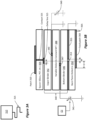
- Figure 1 illustrates a top view of an antenna 100, according to one embodiment.
- the antenna is a multi-layer antenna that includes the patch layer, the true time delay layer, the slotted ground layer and the corporate feed layer, as will be described in more details below. In some instances, additional layers are added, providing multiple polarization, wider bandwidth, etc.
- the various elements of the antenna may be printed or deposited on the insulating substrates.
- the antenna in this particular example comprises a 4x4 array of radiators 110, although any number of radiators in various geometries and arrangements may be used, and a square arrangement of 4x4 elements is chosen only as one example.
- each radiator 110 is a conductive patch provided (e.g., deposited, adhered to, or printed) on top of an insulation layer 105 and has a delay feed line 115 coupled to it, either physically or capacitively, as will be explained further below.
- Each delay feed line 115 is a meandering conductor that provides the RF signal to its corresponding patch 110.
- the RF signal can be manipulated, e.g., delayed, change frequency, change phase, by controlling a variable dielectric layer positioned under the delay line. By controlling all of the delay lines, the array can be made to point to different directions, as needed, thus providing a scanning array.
- each element is fed from only one feed line 115.
- each radiating element 210 can be fed by two orthogonal feed lines, 215 and 217, for example, each having different polarization.
- the description provided herein is applicable to both and any similar, architectures.
- Figures 1 and 2 can be better understood from the following description of Figures 3A and 3B , with further reference to Figure 8 .
- Figure 3A illustrates a top view of a single radiating element 310
- Figure 3B illustrates a cross section of relevant sections of the antenna at the location of the radiating element 310 of Figure 3A .
- Figure 8 provides a top "transparent" view that is applicable to all of the embodiments described herein, including the embodiment of Figures 3A and 3B .
- Figures 1A and 1B illustrate embodiments of the ground plane that may be used in any of the embodiments disclosed herein, as well as the embodiments disclosed in the ⁇ 269 patent.
- a top dielectric spacer 305 is generally in the form of a dielectric (insulating) plate or a dielectric sheet, and may be made of, e.g., glass, PET, etc.
- the radiating patch 310 is formed over the spacer by, e.g., adhering a conductive film, sputtering, printing, etc.
- a via is formed in the dielectric spacer 305 and is filled with conductive material, e.g., copper, to form contact 325, which connects physically and electrically to radiating patch 310.
- a delay line 315 is formed on the bottom surface of dielectric spacer 305 (or on top surface of upper binder 342), and is connected physically and electrically to contact 325.
- the delay line 315 is a meandering conductive line and may take on any shape so as to have sufficient length to generate the desired delay, thereby causing the desired phase shift in the RF signal.
- variable dielectric constant (VDC) plate 340 having variable dielectric constant material 344. While any manner for constructing the VDC plate 340 may be suitable for use with the embodiments of the antenna, as a shorthand in the specific embodiments the VDC plate 340 is shown consisting of upper binder 342, (e.g., glass PET, etc.) variable dielectric constant material 344 (e.g., twisted nematic liquid crystal layer), and bottom binder 346. In other embodiments one or both of the binder layers 342 and 344 may be omitted. Alternatively, adhesive such as epoxy or glass beads may be used instead of the binder layers 342 and/or 344.
- upper binder 342 e.g., glass PET, etc.
- variable dielectric constant material 344 e.g., twisted nematic liquid crystal layer
- bottom binder 346 e.g., twisted nematic liquid crystal layer
- adhesive such as epoxy or glass beads may be used instead of the binder layers 342 and/or 344.
- the VDC plate 340 when using twisted nematic liquid crystal layer, also includes an alignment layer that may be deposited and/or glued onto the bottom of spacer 305, or be formed on the upper binder 342.
- the alignment layer may be a thin layer of material, such as polyimide-based PVA, that is being rubbed or cured with UV radiation in order to align the molecules of the LC at the edges of confining substrates.
- the effective dielectric constant of VDC plate 340 can be controlled by applying DC potential across the VDC plate 340.
- electrodes are formed and are connected to controllable voltage potential.
- controllable voltage potential There are various arrangements to form the electrodes, and several examples will be shown in the disclosed embodiments.
- electrode 347 is shown connected to variable voltage potential 341, while electrode 343 is connected to ground.
- electrode 343 may also be connected to a variable potential 349.
- Figure 3C illustrates a variation wherein the controller issues two signals: a control signal and a ground or common signal. The control signal is applied to the electrode 343, while the common signal is applied to the ground plane 355.
- variable potential 341 and/or variable potential 349 by changing the output voltage of variable potential 341 and/or variable potential 349, one can change the dielectric constant of the VDC material in the vicinity of the electrodes 343 and 347, and thereby change the RF signal traveling over delay line 315.
- Changing the output voltage of variable potential 341 and/or variable potential 349 can be done using a controller, Ctl, running software that causes the controller to output the appropriate control signal to set the appropriate output voltage of variable potential 341 and/or variable potential 349.
- a conventional controller can be used to provide the control and common signals to control the characteristics of the antenna, as shown in Figure 3C .
- the antenna's performance and characteristics can be controlled using software - hence software controlled antenna.
- ground refers to both the generally acceptable ground potential, i.e., earth potential, and also to a common or reference potential, which may be a set potential or a floating potential.
- ground or common signal For example, conventional LCD display controllers output two signals per pixel, one of which is referred to as the ground or common signal.
- the symbol for ground is used, it is used as shorthand to signify either an earth or a common potential, interchangeably.
- common or reference potential which may be set or floating potential
- the RF signal is applied to the feed patch 360 via connector 365 (e.g., a coaxial cable connector).
- connector 365 e.g., a coaxial cable connector
- the layers are designed such that an RF short is provided between the feed patch 360 and delay line 315.
- a back plane conductive ground (or common) 355 is formed on the top surface of backplane insulator (or dielectric) 350 or the bottom surface of bottom binder 346.
- the back plane conductive ground 355 is generally a layer of conductor covering the entire area of the antenna array.
- a window (DC break) 353 is provided in the back plane conductive ground 355.
- the RF signal travels from the feed patch 360, via the window 353, and is coupled to the delay line 315. The reverse happens during reception.
- a DC open and an RF short are formed between delay line 315 and feed patch 360.
- the back plane insulator 350 is made of a Rogers ® (FR-4 printed circuit board) and the feed patch 360 may be a conductive line formed on the Rogers.
- a PTFE Polytetrafluoroethylene or Teflon ®
- other low loss material may be used.
- Figure 8 illustrates an embodiment with two delay lines connected to a single patch 810, such that each delay line may carry a different signal, e.g., at different polarization.
- the following explanation is made with respect to one of the delay lines, as the other may have similar construction.
- the radiating patch 810 is electrically DC connected to the delay line 815 by contact 825 (the delay line for the other feed is referenced as 817). So, in this embodiment the RF signal is transmitted from the delay line 815 to the radiating patch 810 directly via the contact 825. However, no DC connection is made between the feed patch 860 and the delay line 815; rather, the RF signal is capacitively coupled between the feed patch 860 and the delay line 815. This is done through an aperture in the ground plane 850. As shown in Figure 3B , the VDC plate 340 is positioned below the delay line 315, but in Figure 8 it is not shown, so as to simplify the drawing for better understanding of the RF short feature.
- the back ground plane 850 is partially represented by the hatch marks, also showing the window (DC break) 853.
- the RF path is radiating patch 810, to contact 825, to delay line 815, capacitively through window 850 to feed patch 860.
- the length of the window 853, indicated as "L” should be set to about half the wavelength of the RF signal traveling in the feed patch 860, i.e., ⁇ /2.
- the width of the window, indicated as “W”, should be set to about a tenth of the wavelength, i.e., ⁇ /10.
- the feed patch 860 extends about a quarter wave, ⁇ /4, beyond the edge of the window 853, as indicated by D.
- the terminus end (the end opposite contact 825) of delay line 815 extends a quarter wave, ⁇ /4, beyond the edge of the window 853, as indicated by E. Note that distance D is shown longer than distance E, since the RF signal traveling in feed patch 860 has a longer wavelength than the signal traveling in delay line 815.
- every reference to wavelength, ⁇ indicates the wavelength traveling in the related medium, as the wavelength may change as it travels in the various media of the antenna according to its design and the DC potential applied to variable dielectric matter within the antenna.
- FIG. 8A illustrates a variation wherein the RF signal path between the delay line and the radiating patch is capacitive, i.e., there's no physical conductive contact between them.
- a coupling patch 810' is fabricated next to the radiating patch 810.
- the contact 825 forms physical conductive contact between the delay line 815 and coupling patch 810'.
- the coupling of the RF signal between the radiating patch 810 and the coupling patch 810' is capacitive across the short dielectric space S.
- the space S may be simply air or filled with other dielectric material. While in Figure 8A only delay line 815 is shown capacitively coupled to the radiating patch 810, this is done for illustration only, and it should be appreciated that both delay lines 815 and 817 may be capacitively coupled to the radiating patch 810.
- Figure 1A it depicts a top view of a ground plane 155 according to one embodiment.
- the radiating patches 110 and the delay lines 115 are illustrated in dotted lines to enable the reader to orient the elements of the ground plane.
- the ground plane 155 illustrated in Figure 1A may be implemented with any of the other embodiments disclosed herein, including the modified embodiment of the ⁇ 269 patent, as described herein.
- the embodiment of the ground plane 155 illustrated in Figure 1A is particularly useful when utilizing a flat panel display controller (Ctl) to control the VDC pixels of the antenna.
- the controller may be any standard controller that sends a control and a common signal to activate the pixels, e.g., model ZEDV04-E-A from American Zettler Displays, model CBC-2 from Amulet Technologies, model 4171300XX-3 from Digital View, etc.
- Such conventional display controllers operate the refresh the image on the display by sending a common signal to a row of pixels and then serially issuing an activation signal to each pixel in the row. Then it issues a common signal to the next row and serially issues an activation signal to each pixel in the next row.
- the controller can be used in a similar manner to control the pixels of the antenna.
- the ground plane 155 may simply be a plate or a coating of a conductive material, such as copper.
- the conductive material may cover the entire area of the ground plane layer.
- windows 153 may be formed in the ground plane, aligned with the delay lines 115. While for completeness the drawings include the windows 153, the split ground feature disclosed herein may be implemented with or without the coupling windows 153.
- a split ground feature is implemented in the embodiment of Figure 1A .
- elongated DC breaks 157 are formed in the ground plane, dividing the ground plane into rows, indicated in Figure 1A as ground strips 155a-155d.
- Each ground strip 155a-155d is provided under a row of radiating elements and corresponding delay lines.
- Each ground strip 155a-155d is independently connected to the controller.
- the controller can apply common signal to each of the ground strips 155a-155d independently.
- the controller may then apply activation signals serially to the pixels corresponding to the ground strip that receives the common signal.
- each delay line and/or radiating patch there may be more than one pixel, and thus more than one electrode, requiring the applied activation signal. Nevertheless, all of these pixels, and therefore their corresponding electrodes, would be positioned above the strip that receives the common signal. Conversely, as will be described below, the activation signal may be applied to the delay line, thus activating all of the VDC pixels below the delay line simultaneously. It should also be noted that while in Figure 1A the ground strips are shown in a "row” orientation, the same effect can be obtained by arranging the ground strips in "column” orientation.
- a feature of the split ground is that it is accomplished using DC breaks sized to appear as continuity for the RF signal. That is, while the breaks 157 provide isolation for DC signal and for the relatively low frequency square wave of the controller (normally 50Hz-400Hz), it appears as a short for the high frequency RF signal. Consequently, the same ground plane can be used as ground for the RF signal and as common for the pixel control. To accomplish forming a DC break that appears as a short to the RF ground signal, the width of the DC break should not be more than ⁇ /10, with respect to the wavelength of the RF signal traveling in the conductive material.
- embodiments of the invention provide an antenna comprising: an insulating substrate; a plurality of conductive patches provided on top surface of the insulating substrate; a variable dielectric constant (VDC) plate; a plurality of conductive delay lines provided over the VDC plate, each of the delay lines coupling RF signal to one of the plurality of conductive patches; and a ground plane provided below the VDC plate, the ground plane comprising at least one DC break sized to form a short for ground path of the RF signal.
- the VDC plate may define a plurality of VDC pixels, and the antenna may further comprise at least one activation electrode corresponding to each of the plurality of VDC pixels.
- Each of the plurality of delay line may comprise activation signal input configured for receiving activation signal from a controller.
- Each radiating patch may include a conductive stub, each conductive stub being coupled to activation signal line of a controller.
- Each of the elongated rows is independently coupled to a common signal output of a controller.
- the ground plane may comprise a plurality of elongated DC breaks dividing the ground plane to a plurality of ground strips. Similarly, the ground plane may comprise a plurality of DC breaks, each traversing the entire ground plane, thus dividing the ground plane into a plurality of physically separated ground patches. The width of the DC break is not more than ⁇ /10 with respect to the wavelength of the RF signal.
- the ground plane may further comprise a plurality of apertures, each aperture being aligned below one of the conductive delay lines.
- the ground plane may comprise a plurality of DC breaks, each traversing the entire ground plane, thus dividing the ground plane into a plurality of elongated rows, each row being aligned below a row of conductive delay lines.
- split ground embodiment shown in Figure 1A is but one example, but many other designs can be implemented to suit different applications. To illustrate, a couple more examples are discussed below.
- Figure 1B illustrates an example wherein the ground plane is split to provide separate ground strips (155a-155h) for the radiating patches and the delay lines.
- such an arrangement can be used to separately activate VDC pixels below the patches (e.g., to change resonance frequency) and VDC pixels below the delay lines (e.g. to cause scanning or steering of the array). This can be done by the same of a different controller.
- FIG 1C illustrates an example wherein each unit of radiating patch and corresponding delay line is provided its own separate ground patch. Using such an arrangement, the VDC pixels of each unit can be controlled independently by receiving separate activation and common signals. In Figure 1C four ground lines are shown terminating at each row, to indicate that each of the ground patch in the row is connected individually to the controller.
- the split lines can be aligned between the radiating patch and a corresponding delay line.
- Figure 1F showing a split ground plane for an antenna array of 2 ⁇ 2 radiating elements 110.
- the radiating patches 110 and delay lines 115 are shown in dotted lines, as they are in a different layer than the ground plane 155.
- the contact 125 between the radiating patch and corresponding delay line is illustrated as a circle.
- the ground plane includes DC breaks 157 that pass below and in alignment between the radiating element 110 and its corresponding delay line 115, thus creating ground patches 155a-155d, wherein a ground patch, e.g., 155b and 155d, covers an area that encompass a radiating patch and a delay line connected to another radiating patch that overlays a different ground patch.
- a ground patch e.g., 155b and 155d
- a cross DC break is also provided, thus creating a separate ground patch below each of the delay lines. Consequently, the common signal can be delivered independently to each ground path of a specific delay line.
- the coupling windows 153 are also provided in order to couple the RF signal to the delay lines.
- each patch includes a conductive stub 111.
- Each conductive stub 111 is connected to an activation signal line 101 of the controller.
- the signal is transmitted via the activation signal line 101 to the stub 111, thence to the radiating patch 110, thence through the contact 125 to the delay line.
- the ground patch below that delay line receives the common signal, the VDC material between the ground patch and the delay line would be activated.
- the ground plane may be first fabricated as one large conductive coating, e.g., by sputtering or coating with copper or other conductive material. Thereafter the single coating may be etched, scribed, etc., to form the DC breaks.
- the ground plane can be fabricated with the DC breaks, e.g., by using mask during sputtering or coating with copper or other conductor.
- the ground plane may be fabricated as multiple ground patches that are separated from each other by no more than a tenth of the wavelength of the RF signal. The separation distance is configured to appear as a break for a square wave signal of frequency up to 400Hz, but appear as a short for the RF frequencies of the antenna.
- Figure 4 illustrates another embodiment having similar construction to that of Figure 3B , except for the arrangement for applying DC potential to the variable dielectric constant material 444.
- the two electrodes 443 and 447 are provided side by side, rather than across the layer 444.
- the electrodes 443 and 447 can be formed on the top surface of bottom binder 446. Otherwise the structure and operation of the antenna shown in Figure 4 is similar to that shown in Figure 3B .
- Figure 5 illustrates another example designed to provide enhanced bandwidth.
- the general structure of the antenna of Figure 5 can be according to any of the embodiments provided herein, except that another dielectric layer in the form of spacer 514 is provided over the radiating patch 510.
- a resonant path, 512 is formed on top of the spacer 514.
- Resonant patch 512 has the same shape as radiating patch 510, except that it is larger, i.e., has larger width and larger length, if it is a rectangle, or larger sides if it is a square.
- the RF signal is coupled between radiating patch 510 and resonant patch 512 capacitively across spacer 514. This arrangement provides a larger bandwidth than using just radiating patch 510.
- FIGs 6A and 6B illustrate an embodiment having two delay lines connected to each patch, similar to what is shown in Figure 2 .
- each delay line may transmit in different polarization.
- a bottom dielectric 652 separates the two feed patches 660 and 662, each coupling signal to a respective one of the delay lines 615 and 617.
- the two feed patches 660 and 662 are oriented orthogonally to each other.
- the signal coupling is done capacitively through a window 653 in the conductive ground 655, as illustrated in the previous examples.
- Figure 6B only one window 653 is illustrated, since the other window is provided in another plane not shown in this cross section. However, the arrangement of two windows can be seen in Figure 8 .
- the DC break can be made to delineate between the two delay lines, or may have the two delay lines on the same ground patch or ground row.
- Figure 6C illustrates another example of two orthogonal feed lines.
- one feed line is used for transmission while the other is used for reception. While this embodiment is illustrated in conjunction with radiating patch 610 and resonant patch 612, this is not necessary and is used only for consistency of illustration with Figure 6B .
- feed patch 660 is provided on the bottom of backplane dielectric 650 and is coupled to a transmission line via connector 665. The signal from the transmission line 665 is coupled from feed patch 660 capacitively through the window 653 in conductive ground 655 to the radiating patch 610.
- a second conductive ground 655' with window 653' is provided on the bottom of bottom plane dielectric 652.
- conductive ground 655 as a split ground; however, alternatively both conductive grounds 655 and 655' may be split grounds.
- a second bottom plane dielectric 652' is provided below the second conductive ground 655', and feed patch 662 is provided on the bottom of the second bottom plane dielectric 652'.
- feed patch dielectric 662 is used for reception.
- radiating patch 610 is square, so that the transmission and reception are performed at the same frequency, but may be at different polarization and/or phase.
- the radiating patch 610 is rectangle (see Figure 6E ), in which case the transmission and reception may be done at different frequencies, which may be at the same and different polarization and/or phase.
- Figure 6D illustrates another example where one feed patch is used for transmission and the other for reception.
- the control of the VDC material is done by feeding the DC potential to the delay line 615. This can be done, e.g., using a modified Bias-T arrangement.
- Figure 6F illustrates a standard Bias-T circuit.
- the RF + DC node corresponds to the delay line 615.
- the DC node corresponds to the output of the variable voltage potential 641.
- the RF node corresponds to feed patches 660 and 662.
- the RF node is coupled to the circuit via capacitor C.
- the RF signal in the disclosed embodiments is already coupled to the delay line capacitively, such that capacitor C may be omitted.
- inductor I into the DC side of the antenna, a modified Bias-T circuitry is created.
- the common, or ground, signal can be applied to the conductive ground 655, which may be implemented as split ground according to any of the embodiments disclosed herein.
- FIG. 6D Another variation illustrated in Figure 6D , but which can be implemented in any of the other embodiments, is the elimination of the binder layers.
- the VDC material is sandwiched between the spacer 605 and the back plane dielectric 650 with the conductive ground 655.
- glass beads shown in broken line
- glass beads can be interspersed within VDC material 644 so as to maintain the proper separation between the spacer 605 and the back plane dielectric 650 with the conductive ground 655.
- glass beads can also be used when using the binder layers.
- Figure 7 illustrates an embodiment wherein the DC potential for controlling the variable dielectric constant material is applied to the delay line itself, such that no electrodes are needed.
- a standard controller may be used, which provides an activation signal and a common signal to control each pixel.
- a bias-t may be used to separate the RF and activation signals.
- the output of the controller Ctl coupled (e.g., via bias-t) to the delay line 715, establishing a DC potential between delay line 715 and backplane conductive ground 755.
- the backplane conductive ground 755 may be a split ground, as disclosed in the above embodiments, such that the common signal of the controller is applied to a ground strip or a ground patch, depending on the split ground utilized. Consequently, the delay line has two functions: it accepts the DC voltage potential to thereby change the dielectric constant of the VDC material 744, and it capacitively couples RF signal to the feed patches 760 and 762.
- various antennas may be constructed having the common elements comprising: an insulating spacer; at least one radiating arrangement provided on the insulating spacer, wherein each radiating arrangement comprises a conductive patch provided on the top surface of the insulating spacer, a delay line provided on the bottom surface of the insulating spacer, and a contact made of conductive material and providing electrical DC connection between the conductive patch and the delay line via a window in the insulating spacer; a variable dielectric constant (VDC) plate; a back plane insulator; a back plane conductive ground provided over the top surface of the back plane insulator; and an RF coupling arrangement for each of the at least one radiating arrangement, the RF coupling arrangement comprising a window formed in the back plane conductive ground and a conductive RF feed patch provided over the bottom surface of the back plane insulator in an overlapping orientation to the window.
- VDC variable dielectric constant
- electrodes are provided in order to control the dielectric constant at selected areas of the VDC plate, while in others the delay line is used for this purpose.
- the conductive patch is used to couple RF signal from the air, while in others it is used to couple RF energy to another, larger, patch which is used to couple RF signal from the air.
- the size of the patch is configured according to the desired RF wavelength. The RF wavelength can also be used to optimize the RF coupling by properly sizing the window, the delay line, and the feed patch.
- the VDC plate may be segmented into individual pixels of VDC material.
- An LCD panel of a flat panel screen may be used for the VDC plate.
- VDC pixels may be grouped according to the area coverage of the electrodes or the delay lines. In other embodiments the VDC material is provided only in areas controlled by the electrodes or delay line.
- Figure 9 illustrates an example wherein the VDC plate 940 includes only defined area of VDC material.
- VDC area 942 is shown under delay line 915 and VDC area 944 is shown under delay line 917.
- Each of VDC areas may be one continuous area of VDC material or may be divided into pixels. For ease of production the entire area of VDC plate 940 may include pixels of VDC material.
- Figure 9A illustrates capacitive coupling of the delay line 915 to the radiating patch 910 through coupling patch 910', similar to that shown in Figure 8A , but otherwise it is the same as shown in Figure 9 .
- FIG. 10 illustrates an embodiment wherein no VDC plate is used.
- the antenna comprises an insulating substrate 1080 and the conductive patch 1010 is provided on the top surface of the insulating substrate 1080.
- a ground plane 1055 provided on the bottom surface of the insulating substrate 1080, the ground plane comprising an aperture 1053 therein. The aperture is registered to be aligned below the conductive patch 1010.
- a feed line 1060 has its terminative end thereof registered to be aligned below the aperture 1053, so as to capacitively transmit RF signal to the conductive patch 1010 through the aperture 1053.
- a back plane dielectric is provided between the ground plane 1055 and the feed line 1060.
- a connector 1065 is used to transmit/receive RF signal to/from the feed line 1060.
- a multi-layer, software controlled antenna comprises a radiating patch over an insulator plate.
- a delay line is provided on the bottom of the insulator plate and has one end thereof RF coupled to the radiating patch.
- the electrical coupling may be by physical conductive contact or by proximity coupling without physical conductive connection therebetween.
- a variable dielectric constant (VDC) plate is provided below the delay line.
- a ground plane is provided on bottom of VDC plate, the ground plane comprising an aperture therein, the aperture being registered to be aligned below the radiating patch.
- a feed line having terminative end thereof registered to be aligned below the aperture is provided below the ground plane, so as to capacitively transmit RF signal to the conductive patch through the aperture.
- An electrical isolation is provided between the feed line and the ground plane.
- a back plane dielectric plate may be provided between the feed line and the ground plane.
- a second feed line is provided, which may coupled RF signal to the delay line through another aperture provided in the ground plane, or through a second, separate ground plane.
- a resonant patch may be provided over the radiating patch, wherein in some embodiments an insulating spacer may be provided between the radiating patch and the resonant patch.
- electrodes are provided in the VDC plate. The electrodes are coupled to variable voltage potential source, which may be connected to a controller. In other embodiments the VDC plate is controlled by applying DC potential to the delay line. Applying a DC potential to the delay line may be implemented using a modified Biat-T, wherein the feed line, ground plate, VDC plate, and delay line form the RF leg of the Bias-T circuitry. The DC leg may be coupled to the delay line through an intermediate inductor (see Figure 6D ).
- the ground plane may be a split ground plane.
Landscapes
- Engineering & Computer Science (AREA)
- Computer Networks & Wireless Communication (AREA)
- Signal Processing (AREA)
- Physics & Mathematics (AREA)
- Electromagnetism (AREA)
- Power Engineering (AREA)
- Computer Hardware Design (AREA)
- Microelectronics & Electronic Packaging (AREA)
- General Physics & Mathematics (AREA)
- Condensed Matter Physics & Semiconductors (AREA)
- Manufacturing & Machinery (AREA)
- Variable-Direction Aerials And Aerial Arrays (AREA)
- Waveguide Aerials (AREA)
- Details Of Aerials (AREA)
- Liquid Crystal (AREA)
- Production Of Multi-Layered Print Wiring Board (AREA)
- Waveguide Switches, Polarizers, And Phase Shifters (AREA)
Claims (10)
- Antenne comprenant :un substrat isolant (1080, 305) ;une pluralité de plaques conductrices (1010, 310) prévues sur une surface supérieure du substrat isolant (1080) ;une plaque à constante diélectrique variable, VDC, (340) prévue sous le substrat isolant (1080, 305) ;une pluralité de lignes à retard conducteur (315) prévues sur la plaque VDC (340), chacune des lignes à retard (315) couplant un signal RF à l'un de la pluralité de plaques conductrices (1010, 310) ;un plan de masse (355) prévu sous la plaque VDC (340), le plan de masse (355) comprenant au moins une rupture CC (157, 353) dimensionnée pour former un court-circuit pour le chemin de masse du signal RF.
- Antenne selon la revendication 1, dans laquelle chacune de la pluralité de lignes à retard (315) comprend une entrée de signal d'activation configurée pour recevoir un signal d'activation à partir d'un contrôleur (Ctl).
- Antenne selon la revendication 1, dans laquelle le plan de masse (355) comprend une pluralité de ruptures CC allongées (157, 353) divisant le plan de masse à une pluralité de bandes de masse (155a-155d).
- Antenne selon la revendication 1, dans laquelle la largeur de la rupture CC (157, 353) n'est pas supérieure à λ/10 par rapport à la longueur d'onde du signal RF.
- Antenne selon la revendication 1, dans laquelle le plan de masse (355) comprend en outre une pluralité d'ouvertures (1053), chaque ouverture (1053) étant alignée en dessous d'une des lignes à retard conducteur (315).
- Antenne selon la revendication 1, dans laquelle chaque plaque rayonnante (310, 110) comprend un stub conducteur (111), chaque stub conducteur étant couplé à une ligne de signal d'activation d'un contrôleur (Ctl).
- Antenne selon la revendication 1, dans laquelle chaque ligne à retard conducteur (315) est couplée à une ligne de signal d'activation (101) d'un contrôleur (Ctl).
- Antenne selon la revendication 7, comprenant en outre un contrôleur (Ctl), le contrôleur (Ctl) comprenant une pluralité de sorties de signal communes, chaque sortie de signal commun étant couplée à l'une des plaques de masse (155a-155d).
- Antenne selon la revendication 1, dans laquelle le plan de masse (355) comprend une pluralité de ruptures CC (157, 353), chacune traversant le plan de masse entier (355), divisant ainsi le plan de masse (355) en une pluralité de rangées allongées, chaque rangée étant alignée en dessous d'une rangée de lignes à retard conductrices (315).
- Antenne selon la revendication 9, dans laquelle chacune des rangées allongées est couplée indépendamment à une sortie de signal commun d'un contrôleur (Ctl).
Applications Claiming Priority (5)
| Application Number | Priority Date | Filing Date | Title |
|---|---|---|---|
| US201662382506P | 2016-09-01 | 2016-09-01 | |
| US201662382489P | 2016-09-01 | 2016-09-01 | |
| US201662431393P | 2016-12-07 | 2016-12-07 | |
| US15/654,643 US10326205B2 (en) | 2016-09-01 | 2017-07-19 | Multi-layered software defined antenna and method of manufacture |
| PCT/US2018/016872 WO2019018005A1 (fr) | 2016-09-01 | 2018-02-05 | Antenne à constante diélectrique variable ayant une électrode de masse divisée |
Publications (3)
| Publication Number | Publication Date |
|---|---|
| EP3656020A1 EP3656020A1 (fr) | 2020-05-27 |
| EP3656020A4 EP3656020A4 (fr) | 2021-04-28 |
| EP3656020B1 true EP3656020B1 (fr) | 2023-08-30 |
Family
ID=61243623
Family Applications (4)
| Application Number | Title | Priority Date | Filing Date |
|---|---|---|---|
| EP17847150.4A Active EP3507858B1 (fr) | 2016-09-01 | 2017-07-26 | Antenne multicouches définie par logiciel |
| EP17847175.1A Active EP3507856B1 (fr) | 2016-09-01 | 2017-08-02 | Antenne commandée par logiciel |
| EP17847661.0A Active EP3507864B1 (fr) | 2016-09-01 | 2017-09-01 | Procédé de fabrication d'antenne commandée par logiciel |
| EP18836169.5A Active EP3656020B1 (fr) | 2016-09-01 | 2018-02-05 | Antenne à constante diélectrique variable ayant une électrode de masse divisée |
Family Applications Before (3)
| Application Number | Title | Priority Date | Filing Date |
|---|---|---|---|
| EP17847150.4A Active EP3507858B1 (fr) | 2016-09-01 | 2017-07-26 | Antenne multicouches définie par logiciel |
| EP17847175.1A Active EP3507856B1 (fr) | 2016-09-01 | 2017-08-02 | Antenne commandée par logiciel |
| EP17847661.0A Active EP3507864B1 (fr) | 2016-09-01 | 2017-09-01 | Procédé de fabrication d'antenne commandée par logiciel |
Country Status (9)
| Country | Link |
|---|---|
| US (4) | US10326205B2 (fr) |
| EP (4) | EP3507858B1 (fr) |
| JP (6) | JP7045085B2 (fr) |
| KR (5) | KR102375364B1 (fr) |
| CN (4) | CN109964364B (fr) |
| CA (1) | CA3070353A1 (fr) |
| IL (3) | IL261863B (fr) |
| TW (3) | TWI662742B (fr) |
| WO (4) | WO2018044438A1 (fr) |
Families Citing this family (44)
| Publication number | Priority date | Publication date | Assignee | Title |
|---|---|---|---|---|
| CN110140184A (zh) * | 2016-12-07 | 2019-08-16 | 韦弗有限责任公司 | 低损耗电传输机构和使用其的天线 |
| US10446939B2 (en) * | 2017-01-16 | 2019-10-15 | Innolux Corporation | Liquid-crystal antenna apparatus and electronic communication device |
| US10705391B2 (en) * | 2017-08-30 | 2020-07-07 | Wafer Llc | Multi-state control of liquid crystals |
| JP7441471B2 (ja) * | 2017-10-19 | 2024-03-01 | ウェハー エルエルシー | 高分子分散型/せん断配向型位相変調器デバイス |
| CN111316500B (zh) | 2017-10-30 | 2024-01-30 | 韦弗有限责任公司 | 多层液晶相位调制器 |
| EP3788677B1 (fr) * | 2018-05-01 | 2024-07-10 | Wafer LLC | Diélectrique à faible coût pour une transmission électrique et antenne utilisant ce dernier |
| CN108615966B (zh) * | 2018-05-28 | 2020-06-30 | 京东方科技集团股份有限公司 | 一种天线及其制作方法 |
| EP3830605A4 (fr) | 2018-08-02 | 2022-04-13 | Wafer, LLC | Réseau d'antennes à direction de signal d'onde carrée |
| KR102499038B1 (ko) * | 2018-12-06 | 2023-02-13 | 삼성전자주식회사 | 안테나 모듈 |
| CN109687133B (zh) * | 2019-01-08 | 2024-02-20 | 国网福建省电力有限公司南平供电公司 | 一种小型化北斗卫星终端天线 |
| TWI699929B (zh) * | 2019-01-30 | 2020-07-21 | 友達光電股份有限公司 | 天線單元以及天線裝置 |
| KR102091739B1 (ko) * | 2019-02-01 | 2020-03-20 | 주식회사 센서뷰 | 밀리미터파(mmWave) 대역용 전송선로 일체형 저손실 유연 곡면형 및 직각형 다중 포트 안테나 |
| EP3703182B1 (fr) * | 2019-02-27 | 2023-10-11 | ALCAN Systems GmbH | Dispositif de fréquence radio |
| CN111628258A (zh) * | 2019-02-27 | 2020-09-04 | 艾尔康系统有限责任公司 | 射频设备 |
| JP7169914B2 (ja) * | 2019-03-15 | 2022-11-11 | 株式会社ジャパンディスプレイ | アンテナ装置及びフェーズドアレイアンテナ装置 |
| US11258176B2 (en) * | 2019-04-12 | 2022-02-22 | Kymeta Corporation | Non-circular center-fed antenna and method for using the same |
| WO2020217971A1 (fr) * | 2019-04-24 | 2020-10-29 | 株式会社村田製作所 | Module d'antenne et dispositif de communication équipé de celui-ci |
| EP3742555A1 (fr) | 2019-05-23 | 2020-11-25 | Nokia Solutions and Networks Oy | Appareil comprenant une pluralité de dispositifs d'antenne et procédé de fonctionnement d'un tel appareil |
| CN112151944A (zh) * | 2019-06-28 | 2020-12-29 | Oppo广东移动通信有限公司 | 天线模组、电子设备及电子设备的天线频段调节方法 |
| CN112234361B (zh) * | 2019-06-30 | 2023-09-26 | Oppo广东移动通信有限公司 | 壳体组件、天线装置及电子设备 |
| KR102670834B1 (ko) | 2019-07-25 | 2024-05-29 | 엘지디스플레이 주식회사 | 액정을 포함하는 평판 안테나 |
| US11728577B2 (en) * | 2019-11-15 | 2023-08-15 | Wafer Llc | Multi-layered antenna having dual-band patch |
| CN115004476B (zh) * | 2020-01-30 | 2024-04-02 | 株式会社村田制作所 | 天线装置 |
| TWI789672B (zh) * | 2020-02-03 | 2023-01-11 | 仁寶電腦工業股份有限公司 | 信號傳輸裝置與電纜連接電路 |
| CN111403901B (zh) * | 2020-03-16 | 2021-06-15 | Oppo广东移动通信有限公司 | 天线模组及电子设备 |
| WO2021186596A1 (fr) * | 2020-03-18 | 2021-09-23 | 三菱電機株式会社 | Dispositif d'antenne |
| TWI754944B (zh) * | 2020-03-24 | 2022-02-11 | 日本商英幸技術股份有限公司 | 電磁波收發裝置 |
| CN111403908B (zh) * | 2020-03-24 | 2021-06-08 | Oppo广东移动通信有限公司 | 一种天线组件和电子设备 |
| TWI728826B (zh) * | 2020-06-03 | 2021-05-21 | 友達光電股份有限公司 | 自帶濾波功能的可調式平面天線 |
| CN113972490B (zh) * | 2020-07-22 | 2024-05-24 | 上海天马微电子有限公司 | 天线及其制作方法 |
| CN111740200B (zh) * | 2020-07-30 | 2021-01-26 | 南京星腾通信技术有限公司 | 一种基于液晶衬底可连续调相的功分器 |
| TWI749987B (zh) * | 2021-01-05 | 2021-12-11 | 友達光電股份有限公司 | 天線結構及陣列天線模組 |
| US11705627B1 (en) * | 2021-02-26 | 2023-07-18 | Amazon Technologies, Inc. | Antenna module grounding for phased array antennas |
| CN113517572B (zh) * | 2021-03-25 | 2022-09-23 | 西安电子科技大学 | 一种用于毫米波频段的高隔离度双频双极化阵列天线 |
| KR20220152772A (ko) * | 2021-05-10 | 2022-11-17 | 삼성전자주식회사 | 안테나 및 이를 포함하는 전자 장치 |
| KR102509286B1 (ko) * | 2021-05-12 | 2023-03-10 | 영남대학교 산학협력단 | 빔 제어 장치 및 그 제조 방법과 이를 구비하는 통신 장치 |
| US20230187836A1 (en) * | 2021-11-19 | 2023-06-15 | Sderotech, Inc. | Variable dielectric based antenna with improved response time |
| KR102629717B1 (ko) * | 2022-02-28 | 2024-01-29 | 한국과학기술원 | 주파수 가변 범위 확장 및 방사부 소형화를 위한 액정 기반 마이크로스트립 패치 안테나 |
| JP7245947B1 (ja) * | 2022-08-15 | 2023-03-24 | Fcnt株式会社 | 印刷配線基板及び無線通信端末 |
| WO2024037707A1 (fr) * | 2022-08-16 | 2024-02-22 | Huawei Technologies Co., Ltd. | Antennes à motif maillé sur verre pour couvercle arrière et directions d'affichage utilisant des trous d'interconnexion en verre traversants |
| WO2024173757A1 (fr) * | 2023-02-17 | 2024-08-22 | Carillon Technologies Management Corporation | Réseau d'antennes |
| WO2024180375A1 (fr) * | 2023-02-28 | 2024-09-06 | Gachahi Alex | Antenne à électro-aimant capacitif (antenne cem) |
| CN116683202B (zh) * | 2023-07-21 | 2024-05-14 | 广东博纬通信科技有限公司 | 一种多波束阵列天线 |
| US11955719B1 (en) | 2023-12-11 | 2024-04-09 | United Arab Emirates University | Antenna system comprising two oppositely directed antennas and methods for controlling transmission of radiation through a multi-layered antenna structure |
Family Cites Families (80)
| Publication number | Priority date | Publication date | Assignee | Title |
|---|---|---|---|---|
| US4684952A (en) * | 1982-09-24 | 1987-08-04 | Ball Corporation | Microstrip reflectarray for satellite communication and radar cross-section enhancement or reduction |
| JPS633612U (fr) * | 1986-06-24 | 1988-01-11 | ||
| US5223849A (en) * | 1986-11-25 | 1993-06-29 | Chomerics, Inc. | Broadband electromagnetic energy absorber |
| US5043738A (en) * | 1990-03-15 | 1991-08-27 | Hughes Aircraft Company | Plural frequency patch antenna assembly |
| DE4239597C2 (de) * | 1991-11-26 | 1999-11-04 | Hitachi Chemical Co Ltd | Ebene Antenne mit dualer Polarisation |
| JPH08181539A (ja) * | 1994-12-26 | 1996-07-12 | Toyo Commun Equip Co Ltd | 円偏波マイクロストリップアンテナ |
| US6384785B1 (en) * | 1995-05-29 | 2002-05-07 | Nippon Telegraph And Telephone Corporation | Heterogeneous multi-lamination microstrip antenna |
| JP3194468B2 (ja) * | 1995-05-29 | 2001-07-30 | 日本電信電話株式会社 | マイクロストリップアンテナ |
| US5617103A (en) * | 1995-07-19 | 1997-04-01 | The United States Of America As Represented By The Secretary Of The Army | Ferroelectric phase shifting antenna array |
| JP3323087B2 (ja) * | 1996-11-29 | 2002-09-09 | 京セラ株式会社 | 高周波伝送線路の結合構造 |
| DE19628125A1 (de) * | 1996-07-12 | 1998-01-15 | Daimler Benz Ag | Aktive Empfangsantenne |
| SE507076C2 (sv) * | 1997-01-24 | 1998-03-23 | Allgon Ab | Antennelement |
| JPH1174717A (ja) * | 1997-06-23 | 1999-03-16 | Nec Corp | フェーズドアレーアンテナ装置 |
| US6154176A (en) * | 1998-08-07 | 2000-11-28 | Sarnoff Corporation | Antennas formed using multilayer ceramic substrates |
| JP3552971B2 (ja) | 1998-12-14 | 2004-08-11 | 松下電器産業株式会社 | アクティブフェイズドアレイアンテナ |
| JP3874964B2 (ja) | 1999-04-28 | 2007-01-31 | 日本放送協会 | 可変移相器 |
| JP2000341027A (ja) | 1999-05-27 | 2000-12-08 | Nippon Hoso Kyokai <Nhk> | パッチアンテナ装置 |
| JP2003509937A (ja) * | 1999-09-14 | 2003-03-11 | パラテック マイクロウェーブ インコーポレイテッド | 誘電体移相器を有する直列給電フェーズドアレイアンテナ |
| JP3535423B2 (ja) | 1999-10-18 | 2004-06-07 | 三菱電機株式会社 | レドーム |
| JP3588297B2 (ja) | 2000-02-14 | 2004-11-10 | 日本電信電話株式会社 | アンテナ装置 |
| US6653776B1 (en) * | 2000-06-28 | 2003-11-25 | International Business Machines Corporation | Discrete magnets in dielectric forming metal/ceramic laminate and process thereof |
| JP2002033617A (ja) | 2001-06-01 | 2002-01-31 | Mitsubishi Electric Corp | 給電装置 |
| JP4070428B2 (ja) | 2001-07-04 | 2008-04-02 | 日本放送協会 | 周波数可変フィルタ |
| US20030184477A1 (en) * | 2002-03-29 | 2003-10-02 | Lotfollah Shafai | Phased array antenna steering arrangements |
| JP2004023228A (ja) | 2002-06-13 | 2004-01-22 | Matsushita Electric Ind Co Ltd | アンテナ制御装置、及びフェイズドアレイアンテナ |
| US6703114B1 (en) * | 2002-10-17 | 2004-03-09 | Arlon | Laminate structures, methods for production thereof and uses therefor |
| JP2004146908A (ja) | 2002-10-22 | 2004-05-20 | Sharp Corp | マイクロストリップアンテナ |
| US6727855B1 (en) * | 2002-11-21 | 2004-04-27 | The United States Of America As Represented By The Secretary Of The Army | Folded multilayer electrically small microstrip antenna |
| US6842140B2 (en) * | 2002-12-03 | 2005-01-11 | Harris Corporation | High efficiency slot fed microstrip patch antenna |
| US7930815B2 (en) * | 2003-04-11 | 2011-04-26 | Avery Dennison Corporation | Conductive pattern and method of making |
| JP3843081B2 (ja) * | 2003-05-16 | 2006-11-08 | 株式会社インテリジェント・コスモス研究機構 | Nrdガイド変換器 |
| JP2005012554A (ja) | 2003-06-19 | 2005-01-13 | Kyocera Corp | アンテナ基板およびアンテナ装置 |
| US7084828B2 (en) * | 2003-08-27 | 2006-08-01 | Harris Corporation | Shaped ground plane for dynamically reconfigurable aperture coupled antenna |
| US7109928B1 (en) * | 2005-03-30 | 2006-09-19 | The United States Of America As Represented By The Secretary Of The Air Force | Conformal microstrip leaky wave antenna |
| US20090278744A1 (en) | 2005-10-11 | 2009-11-12 | Panasonic Corporation | Phased array antenna |
| JP2007295044A (ja) * | 2006-04-20 | 2007-11-08 | Matsushita Electric Ind Co Ltd | フェーズドアレイアンテナ |
| JP2007110256A (ja) * | 2005-10-11 | 2007-04-26 | Matsushita Electric Ind Co Ltd | フェーズドアレイアンテナ |
| JP4946150B2 (ja) | 2006-02-08 | 2012-06-06 | 日立化成工業株式会社 | 電磁界結合構造及び多層配線板 |
| JP4537339B2 (ja) * | 2006-03-31 | 2010-09-01 | 京セラ株式会社 | 移相器ならびにこれを備える高周波送信器、高周波受信器、高周波送受信器、レーダ装置およびアンテナ装置 |
| JP4053585B2 (ja) * | 2006-04-03 | 2008-02-27 | 松下電器産業株式会社 | 差動給電スロットアンテナ |
| CN101479887A (zh) * | 2006-05-24 | 2009-07-08 | 韦夫班德尔公司 | 集成波导管天线和阵列 |
| JP2009538561A (ja) * | 2006-05-24 | 2009-11-05 | ウェーブベンダー インコーポレーテッド | 一体型導波管アンテナ及びアレイ |
| US7466269B2 (en) * | 2006-05-24 | 2008-12-16 | Wavebender, Inc. | Variable dielectric constant-based antenna and array |
| KR100859711B1 (ko) * | 2006-12-08 | 2008-09-23 | 한국전자통신연구원 | 개구결합 급전방식을 이용한 rfid 센서 태그 안테나 |
| US20100060421A1 (en) * | 2008-09-08 | 2010-03-11 | Chih-Chen Chang | Rfid tag with a semi-enclosed coupler |
| JP5131703B2 (ja) | 2009-02-13 | 2013-01-30 | 株式会社フジクラ | アンテナ製造方法 |
| JP5463354B2 (ja) * | 2009-05-29 | 2014-04-09 | 株式会社Nttドコモ | リフレクトアレイ |
| CN101930134B (zh) | 2009-06-19 | 2013-08-07 | 台均科技(深圳)有限公司 | 电磁感应式液晶面板及其制造方法和液晶显示器 |
| JP4900537B2 (ja) | 2009-07-09 | 2012-03-21 | 株式会社村田製作所 | アンテナ |
| US8279611B2 (en) * | 2009-12-09 | 2012-10-02 | Research In Motion Limited | Flexible cable having rectangular waveguide formed therein and methods of manufacturing same |
| JP2011176545A (ja) | 2010-02-24 | 2011-09-08 | Toppan Printing Co Ltd | 金属装荷型icタグ |
| US9190738B2 (en) * | 2010-04-11 | 2015-11-17 | Broadcom Corporation | Projected artificial magnetic mirror |
| JP2012019421A (ja) | 2010-07-09 | 2012-01-26 | Furukawa Electric Co Ltd:The | アンテナ装置 |
| US8786496B2 (en) * | 2010-07-28 | 2014-07-22 | Toyota Motor Engineering & Manufacturing North America, Inc. | Three-dimensional array antenna on a substrate with enhanced backlobe suppression for mm-wave automotive applications |
| JP5655487B2 (ja) * | 2010-10-13 | 2015-01-21 | 日本電気株式会社 | アンテナ装置 |
| US8730226B2 (en) * | 2010-11-04 | 2014-05-20 | Scanvue Technologies, Llc | Thin-film transistor liquid-crystal display with variable frame frequency |
| ES2388213B2 (es) | 2010-12-16 | 2013-01-29 | Universidad Politécnica de Madrid | Antena reflectarray de haz reconfigurable para frecuencias en los rangos de terahercios y de ondas milimétricas. |
| JP2012182591A (ja) | 2011-02-28 | 2012-09-20 | Kyocer Slc Technologies Corp | アンテナ基板 |
| CN102959801A (zh) * | 2011-04-19 | 2013-03-06 | 华为技术有限公司 | 一种微带天线 |
| US8922297B2 (en) * | 2011-06-22 | 2014-12-30 | The Boeing Company | Multi-conductor transmission lines for control-integrated RF distribution networks |
| US8928542B2 (en) * | 2011-08-17 | 2015-01-06 | CBF Networks, Inc. | Backhaul radio with an aperture-fed antenna assembly |
| EP2575211B1 (fr) * | 2011-09-27 | 2014-11-05 | Technische Universität Darmstadt | Antenne de réseau phasée planaire orientable électroniquement |
| IL218625A (en) * | 2012-03-14 | 2017-10-31 | Israel Aerospace Ind Ltd | An antenna array |
| KR101744605B1 (ko) * | 2012-11-07 | 2017-06-08 | 가부시키가이샤 무라타 세이사쿠쇼 | 어레이 안테나 |
| JP6033106B2 (ja) | 2013-02-12 | 2016-11-30 | 三菱電機株式会社 | アンテナ装置 |
| EP2768072A1 (fr) * | 2013-02-15 | 2014-08-20 | Technische Universität Darmstadt | Déphaseur |
| CN103259093B (zh) * | 2013-04-09 | 2015-05-06 | 重庆金美通信有限责任公司 | 一种抑制表面波的宽频带微带天线 |
| US9941593B2 (en) * | 2013-04-30 | 2018-04-10 | Monarch Antenna, Inc. | Patch antenna and method for impedance, frequency and pattern tuning |
| US9240631B2 (en) * | 2013-09-11 | 2016-01-19 | Michael Westick Westrick | Reduced ground plane shorted-patch hemispherical omni antenna |
| US9887456B2 (en) * | 2014-02-19 | 2018-02-06 | Kymeta Corporation | Dynamic polarization and coupling control from a steerable cylindrically fed holographic antenna |
| WO2015172841A1 (fr) * | 2014-05-16 | 2015-11-19 | Huawei Technologies Co., Ltd. | Antenne multicouche plane |
| KR102413786B1 (ko) | 2014-11-17 | 2022-06-28 | 알파마이크론, 인크. | 가요성 전기-광학 셀의 생산 방법 |
| US9502780B2 (en) * | 2015-01-15 | 2016-11-22 | Northrop Grumman Systems Corporation | Antenna array using sandwiched radiating elements above a ground plane and fed by a stripline |
| US9893435B2 (en) * | 2015-02-11 | 2018-02-13 | Kymeta Corporation | Combined antenna apertures allowing simultaneous multiple antenna functionality |
| GB2535216B (en) * | 2015-02-13 | 2019-04-24 | Cambium Networks Ltd | Antenna array assembly using a dielectric film and a ground plate with a contoured surface |
| CN104953256B (zh) * | 2015-05-25 | 2018-01-12 | 电子科技大学 | 宽带圆极化平板阵列天线 |
| JP6139045B1 (ja) * | 2016-01-29 | 2017-05-31 | シャープ株式会社 | 走査アンテナ |
| US9726631B1 (en) * | 2016-02-09 | 2017-08-08 | International Business Machines Corporation | Ultra-sensitive biosensor based on lateral bipolar junction transistor having self-aligned epitaxially grown base |
| US10686257B2 (en) * | 2016-09-01 | 2020-06-16 | Wafer Llc | Method of manufacturing software controlled antenna |
| CN106299627B (zh) * | 2016-10-18 | 2023-06-02 | 京东方科技集团股份有限公司 | 一种液晶天线及通信设备 |
-
2017
- 2017-07-19 US US15/654,643 patent/US10326205B2/en active Active
- 2017-07-20 TW TW106124276A patent/TWI662742B/zh active
- 2017-07-26 KR KR1020197008781A patent/KR102375364B1/ko active IP Right Grant
- 2017-07-26 EP EP17847150.4A patent/EP3507858B1/fr active Active
- 2017-07-26 WO PCT/US2017/044045 patent/WO2018044438A1/fr unknown
- 2017-07-26 JP JP2019511934A patent/JP7045085B2/ja active Active
- 2017-07-26 CN CN201780061375.0A patent/CN109964364B/zh not_active Expired - Fee Related
- 2017-08-02 EP EP17847175.1A patent/EP3507856B1/fr active Active
- 2017-08-02 KR KR1020197007515A patent/KR102479625B1/ko active IP Right Grant
- 2017-08-02 CN CN201780061159.6A patent/CN109937511B/zh active Active
- 2017-08-02 WO PCT/US2017/045186 patent/WO2018044488A1/fr unknown
- 2017-08-02 JP JP2019511937A patent/JP2019537850A/ja active Pending
- 2017-08-02 US US15/667,584 patent/US10177453B2/en active Active
- 2017-08-03 TW TW106126192A patent/TWI691116B/zh active
- 2017-09-01 CN CN201780020915.0A patent/CN109075443B/zh active Active
- 2017-09-01 JP JP2018548180A patent/JP6591088B2/ja active Active
- 2017-09-01 EP EP17847661.0A patent/EP3507864B1/fr active Active
- 2017-09-01 WO PCT/US2017/049962 patent/WO2018045350A1/fr unknown
- 2017-09-01 KR KR1020187028100A patent/KR102072934B1/ko active IP Right Grant
-
2018
- 2018-02-05 EP EP18836169.5A patent/EP3656020B1/fr active Active
- 2018-02-05 JP JP2020502472A patent/JP7002630B2/ja active Active
- 2018-02-05 WO PCT/US2018/016872 patent/WO2019018005A1/fr unknown
- 2018-02-05 KR KR1020237003522A patent/KR20230028805A/ko not_active Application Discontinuation
- 2018-02-05 KR KR1020207004088A patent/KR20200090142A/ko not_active Application Discontinuation
- 2018-02-05 CA CA3070353A patent/CA3070353A1/fr active Pending
- 2018-02-05 CN CN201880057552.2A patent/CN111095676B/zh active Active
- 2018-02-08 TW TW107104565A patent/TWI672859B/zh not_active IP Right Cessation
- 2018-09-20 IL IL261863A patent/IL261863B/en unknown
-
2019
- 2019-02-28 IL IL265111A patent/IL265111B2/en unknown
- 2019-02-28 IL IL265113A patent/IL265113B2/en unknown
- 2019-06-11 US US16/438,303 patent/US10505280B2/en active Active
- 2019-09-17 JP JP2019168502A patent/JP7045080B2/ja active Active
- 2019-12-09 US US16/708,354 patent/US10741921B2/en active Active
-
2022
- 2022-06-15 JP JP2022096587A patent/JP7442850B2/ja active Active
Also Published As
Similar Documents
| Publication | Publication Date | Title |
|---|---|---|
| EP3656020B1 (fr) | Antenne à constante diélectrique variable ayant une électrode de masse divisée | |
| US10505273B2 (en) | Variable dielectric constant antenna having split ground electrode | |
| EP3504754B1 (fr) | Méta-surface accordable à cristaux liquides pour antennes de direction de faisceau | |
| JP7307070B2 (ja) | フェーズドアレイアンテナ、表示パネル及び表示装置 | |
| EP3676908B1 (fr) | Commande à états multiples de cristaux liquides | |
| EP3823094A1 (fr) | Antenne multicouche dotée d'une plaque à deux bandes | |
| US10511096B2 (en) | Low cost dielectric for electrical transmission and antenna using same | |
| EP3788677B1 (fr) | Diélectrique à faible coût pour une transmission électrique et antenne utilisant ce dernier |
Legal Events
| Date | Code | Title | Description |
|---|---|---|---|
| STAA | Information on the status of an ep patent application or granted ep patent |
Free format text: STATUS: THE INTERNATIONAL PUBLICATION HAS BEEN MADE |
|
| PUAI | Public reference made under article 153(3) epc to a published international application that has entered the european phase |
Free format text: ORIGINAL CODE: 0009012 |
|
| STAA | Information on the status of an ep patent application or granted ep patent |
Free format text: STATUS: REQUEST FOR EXAMINATION WAS MADE |
|
| 17P | Request for examination filed |
Effective date: 20200218 |
|
| AK | Designated contracting states |
Kind code of ref document: A1 Designated state(s): AL AT BE BG CH CY CZ DE DK EE ES FI FR GB GR HR HU IE IS IT LI LT LU LV MC MK MT NL NO PL PT RO RS SE SI SK SM TR |
|
| AX | Request for extension of the european patent |
Extension state: BA ME |
|
| DAV | Request for validation of the european patent (deleted) | ||
| DAX | Request for extension of the european patent (deleted) | ||
| A4 | Supplementary search report drawn up and despatched |
Effective date: 20210329 |
|
| RIC1 | Information provided on ipc code assigned before grant |
Ipc: H01P 3/08 20060101AFI20210323BHEP Ipc: H01P 1/18 20060101ALI20210323BHEP Ipc: H05K 3/36 20060101ALI20210323BHEP Ipc: H01Q 3/44 20060101ALI20210323BHEP Ipc: H01Q 21/06 20060101ALI20210323BHEP Ipc: H01Q 9/04 20060101ALI20210323BHEP Ipc: H04B 3/56 20060101ALI20210323BHEP |
|
| REG | Reference to a national code |
Ref country code: DE Ref legal event code: R079 Ref document number: 602018056624 Country of ref document: DE Free format text: PREVIOUS MAIN CLASS: H01Q0021060000 Ipc: H01Q0001480000 Ref legal event code: R079 |
|
| GRAP | Despatch of communication of intention to grant a patent |
Free format text: ORIGINAL CODE: EPIDOSNIGR1 |
|
| STAA | Information on the status of an ep patent application or granted ep patent |
Free format text: STATUS: GRANT OF PATENT IS INTENDED |
|
| RIC1 | Information provided on ipc code assigned before grant |
Ipc: H01Q 21/00 20060101ALI20230224BHEP Ipc: H01Q 21/24 20060101ALI20230224BHEP Ipc: H01Q 21/06 20060101ALI20230224BHEP Ipc: H01Q 9/14 20060101ALI20230224BHEP Ipc: H01Q 9/04 20060101ALI20230224BHEP Ipc: H01Q 3/44 20060101ALI20230224BHEP Ipc: H01Q 3/36 20060101ALI20230224BHEP Ipc: H01Q 1/50 20060101ALI20230224BHEP Ipc: H01Q 1/48 20060101AFI20230224BHEP |
|
| INTG | Intention to grant announced |
Effective date: 20230322 |
|
| GRAS | Grant fee paid |
Free format text: ORIGINAL CODE: EPIDOSNIGR3 |
|
| GRAA | (expected) grant |
Free format text: ORIGINAL CODE: 0009210 |
|
| STAA | Information on the status of an ep patent application or granted ep patent |
Free format text: STATUS: THE PATENT HAS BEEN GRANTED |
|
| AK | Designated contracting states |
Kind code of ref document: B1 Designated state(s): AL AT BE BG CH CY CZ DE DK EE ES FI FR GB GR HR HU IE IS IT LI LT LU LV MC MK MT NL NO PL PT RO RS SE SI SK SM TR |
|
| REG | Reference to a national code |
Ref country code: GB Ref legal event code: FG4D |
|
| REG | Reference to a national code |
Ref country code: CH Ref legal event code: EP |
|
| REG | Reference to a national code |
Ref country code: DE Ref legal event code: R096 Ref document number: 602018056624 Country of ref document: DE |
|
| REG | Reference to a national code |
Ref country code: IE Ref legal event code: FG4D |
|
| REG | Reference to a national code |
Ref country code: LT Ref legal event code: MG9D |
|
| REG | Reference to a national code |
Ref country code: NL Ref legal event code: MP Effective date: 20230830 |
|
| REG | Reference to a national code |
Ref country code: AT Ref legal event code: MK05 Ref document number: 1606636 Country of ref document: AT Kind code of ref document: T Effective date: 20230830 |
|
| PG25 | Lapsed in a contracting state [announced via postgrant information from national office to epo] |
Ref country code: GR Free format text: LAPSE BECAUSE OF FAILURE TO SUBMIT A TRANSLATION OF THE DESCRIPTION OR TO PAY THE FEE WITHIN THE PRESCRIBED TIME-LIMIT Effective date: 20231201 |
|
| PG25 | Lapsed in a contracting state [announced via postgrant information from national office to epo] |
Ref country code: IS Free format text: LAPSE BECAUSE OF FAILURE TO SUBMIT A TRANSLATION OF THE DESCRIPTION OR TO PAY THE FEE WITHIN THE PRESCRIBED TIME-LIMIT Effective date: 20231230 |
|
| PG25 | Lapsed in a contracting state [announced via postgrant information from national office to epo] |
Ref country code: SE Free format text: LAPSE BECAUSE OF FAILURE TO SUBMIT A TRANSLATION OF THE DESCRIPTION OR TO PAY THE FEE WITHIN THE PRESCRIBED TIME-LIMIT Effective date: 20230830 Ref country code: RS Free format text: LAPSE BECAUSE OF FAILURE TO SUBMIT A TRANSLATION OF THE DESCRIPTION OR TO PAY THE FEE WITHIN THE PRESCRIBED TIME-LIMIT Effective date: 20230830 Ref country code: NO Free format text: LAPSE BECAUSE OF FAILURE TO SUBMIT A TRANSLATION OF THE DESCRIPTION OR TO PAY THE FEE WITHIN THE PRESCRIBED TIME-LIMIT Effective date: 20231130 Ref country code: LV Free format text: LAPSE BECAUSE OF FAILURE TO SUBMIT A TRANSLATION OF THE DESCRIPTION OR TO PAY THE FEE WITHIN THE PRESCRIBED TIME-LIMIT Effective date: 20230830 Ref country code: LT Free format text: LAPSE BECAUSE OF FAILURE TO SUBMIT A TRANSLATION OF THE DESCRIPTION OR TO PAY THE FEE WITHIN THE PRESCRIBED TIME-LIMIT Effective date: 20230830 Ref country code: IS Free format text: LAPSE BECAUSE OF FAILURE TO SUBMIT A TRANSLATION OF THE DESCRIPTION OR TO PAY THE FEE WITHIN THE PRESCRIBED TIME-LIMIT Effective date: 20231230 Ref country code: HR Free format text: LAPSE BECAUSE OF FAILURE TO SUBMIT A TRANSLATION OF THE DESCRIPTION OR TO PAY THE FEE WITHIN THE PRESCRIBED TIME-LIMIT Effective date: 20230830 Ref country code: GR Free format text: LAPSE BECAUSE OF FAILURE TO SUBMIT A TRANSLATION OF THE DESCRIPTION OR TO PAY THE FEE WITHIN THE PRESCRIBED TIME-LIMIT Effective date: 20231201 Ref country code: FI Free format text: LAPSE BECAUSE OF FAILURE TO SUBMIT A TRANSLATION OF THE DESCRIPTION OR TO PAY THE FEE WITHIN THE PRESCRIBED TIME-LIMIT Effective date: 20230830 Ref country code: AT Free format text: LAPSE BECAUSE OF FAILURE TO SUBMIT A TRANSLATION OF THE DESCRIPTION OR TO PAY THE FEE WITHIN THE PRESCRIBED TIME-LIMIT Effective date: 20230830 |
|
| PG25 | Lapsed in a contracting state [announced via postgrant information from national office to epo] |
Ref country code: PL Free format text: LAPSE BECAUSE OF FAILURE TO SUBMIT A TRANSLATION OF THE DESCRIPTION OR TO PAY THE FEE WITHIN THE PRESCRIBED TIME-LIMIT Effective date: 20230830 Ref country code: NL Free format text: LAPSE BECAUSE OF FAILURE TO SUBMIT A TRANSLATION OF THE DESCRIPTION OR TO PAY THE FEE WITHIN THE PRESCRIBED TIME-LIMIT Effective date: 20230830 |
|
| PG25 | Lapsed in a contracting state [announced via postgrant information from national office to epo] |
Ref country code: ES Free format text: LAPSE BECAUSE OF FAILURE TO SUBMIT A TRANSLATION OF THE DESCRIPTION OR TO PAY THE FEE WITHIN THE PRESCRIBED TIME-LIMIT Effective date: 20230830 |
|
| PG25 | Lapsed in a contracting state [announced via postgrant information from national office to epo] |
Ref country code: SM Free format text: LAPSE BECAUSE OF FAILURE TO SUBMIT A TRANSLATION OF THE DESCRIPTION OR TO PAY THE FEE WITHIN THE PRESCRIBED TIME-LIMIT Effective date: 20230830 Ref country code: RO Free format text: LAPSE BECAUSE OF FAILURE TO SUBMIT A TRANSLATION OF THE DESCRIPTION OR TO PAY THE FEE WITHIN THE PRESCRIBED TIME-LIMIT Effective date: 20230830 Ref country code: ES Free format text: LAPSE BECAUSE OF FAILURE TO SUBMIT A TRANSLATION OF THE DESCRIPTION OR TO PAY THE FEE WITHIN THE PRESCRIBED TIME-LIMIT Effective date: 20230830 Ref country code: EE Free format text: LAPSE BECAUSE OF FAILURE TO SUBMIT A TRANSLATION OF THE DESCRIPTION OR TO PAY THE FEE WITHIN THE PRESCRIBED TIME-LIMIT Effective date: 20230830 Ref country code: DK Free format text: LAPSE BECAUSE OF FAILURE TO SUBMIT A TRANSLATION OF THE DESCRIPTION OR TO PAY THE FEE WITHIN THE PRESCRIBED TIME-LIMIT Effective date: 20230830 Ref country code: CZ Free format text: LAPSE BECAUSE OF FAILURE TO SUBMIT A TRANSLATION OF THE DESCRIPTION OR TO PAY THE FEE WITHIN THE PRESCRIBED TIME-LIMIT Effective date: 20230830 Ref country code: PT Free format text: LAPSE BECAUSE OF FAILURE TO SUBMIT A TRANSLATION OF THE DESCRIPTION OR TO PAY THE FEE WITHIN THE PRESCRIBED TIME-LIMIT Effective date: 20240102 Ref country code: SK Free format text: LAPSE BECAUSE OF FAILURE TO SUBMIT A TRANSLATION OF THE DESCRIPTION OR TO PAY THE FEE WITHIN THE PRESCRIBED TIME-LIMIT Effective date: 20230830 |
|
| PG25 | Lapsed in a contracting state [announced via postgrant information from national office to epo] |
Ref country code: IT Free format text: LAPSE BECAUSE OF FAILURE TO SUBMIT A TRANSLATION OF THE DESCRIPTION OR TO PAY THE FEE WITHIN THE PRESCRIBED TIME-LIMIT Effective date: 20230830 |
|
| REG | Reference to a national code |
Ref country code: DE Ref legal event code: R097 Ref document number: 602018056624 Country of ref document: DE |
|
| PLBE | No opposition filed within time limit |
Free format text: ORIGINAL CODE: 0009261 |
|
| STAA | Information on the status of an ep patent application or granted ep patent |
Free format text: STATUS: NO OPPOSITION FILED WITHIN TIME LIMIT |
|
| PG25 | Lapsed in a contracting state [announced via postgrant information from national office to epo] |
Ref country code: SI Free format text: LAPSE BECAUSE OF FAILURE TO SUBMIT A TRANSLATION OF THE DESCRIPTION OR TO PAY THE FEE WITHIN THE PRESCRIBED TIME-LIMIT Effective date: 20230830 |
|
| 26N | No opposition filed |
Effective date: 20240603 |