EP3640976A1 - Maske und verfahren zur herstellung eines arraysubstrats - Google Patents
Maske und verfahren zur herstellung eines arraysubstrats Download PDFInfo
- Publication number
- EP3640976A1 EP3640976A1 EP17908931.3A EP17908931A EP3640976A1 EP 3640976 A1 EP3640976 A1 EP 3640976A1 EP 17908931 A EP17908931 A EP 17908931A EP 3640976 A1 EP3640976 A1 EP 3640976A1
- Authority
- EP
- European Patent Office
- Prior art keywords
- area
- sub
- photoresist
- areas
- mask plate
- Prior art date
- Legal status (The legal status is an assumption and is not a legal conclusion. Google has not performed a legal analysis and makes no representation as to the accuracy of the status listed.)
- Withdrawn
Links
Images
Classifications
-
- G—PHYSICS
- G03—PHOTOGRAPHY; CINEMATOGRAPHY; ANALOGOUS TECHNIQUES USING WAVES OTHER THAN OPTICAL WAVES; ELECTROGRAPHY; HOLOGRAPHY
- G03F—PHOTOMECHANICAL PRODUCTION OF TEXTURED OR PATTERNED SURFACES, e.g. FOR PRINTING, FOR PROCESSING OF SEMICONDUCTOR DEVICES; MATERIALS THEREFOR; ORIGINALS THEREFOR; APPARATUS SPECIALLY ADAPTED THEREFOR
- G03F1/00—Originals for photomechanical production of textured or patterned surfaces, e.g., masks, photo-masks, reticles; Mask blanks or pellicles therefor; Containers specially adapted therefor; Preparation thereof
- G03F1/50—Mask blanks not covered by G03F1/20 - G03F1/34; Preparation thereof
-
- G—PHYSICS
- G03—PHOTOGRAPHY; CINEMATOGRAPHY; ANALOGOUS TECHNIQUES USING WAVES OTHER THAN OPTICAL WAVES; ELECTROGRAPHY; HOLOGRAPHY
- G03F—PHOTOMECHANICAL PRODUCTION OF TEXTURED OR PATTERNED SURFACES, e.g. FOR PRINTING, FOR PROCESSING OF SEMICONDUCTOR DEVICES; MATERIALS THEREFOR; ORIGINALS THEREFOR; APPARATUS SPECIALLY ADAPTED THEREFOR
- G03F7/00—Photomechanical, e.g. photolithographic, production of textured or patterned surfaces, e.g. printing surfaces; Materials therefor, e.g. comprising photoresists; Apparatus specially adapted therefor
- G03F7/20—Exposure; Apparatus therefor
- G03F7/2051—Exposure without an original mask, e.g. using a programmed deflection of a point source, by scanning, by drawing with a light beam, using an addressed light or corpuscular source
- G03F7/2059—Exposure without an original mask, e.g. using a programmed deflection of a point source, by scanning, by drawing with a light beam, using an addressed light or corpuscular source using a scanning corpuscular radiation beam, e.g. an electron beam
- G03F7/2063—Exposure without an original mask, e.g. using a programmed deflection of a point source, by scanning, by drawing with a light beam, using an addressed light or corpuscular source using a scanning corpuscular radiation beam, e.g. an electron beam for the production of exposure masks or reticles
-
- G—PHYSICS
- G03—PHOTOGRAPHY; CINEMATOGRAPHY; ANALOGOUS TECHNIQUES USING WAVES OTHER THAN OPTICAL WAVES; ELECTROGRAPHY; HOLOGRAPHY
- G03F—PHOTOMECHANICAL PRODUCTION OF TEXTURED OR PATTERNED SURFACES, e.g. FOR PRINTING, FOR PROCESSING OF SEMICONDUCTOR DEVICES; MATERIALS THEREFOR; ORIGINALS THEREFOR; APPARATUS SPECIALLY ADAPTED THEREFOR
- G03F1/00—Originals for photomechanical production of textured or patterned surfaces, e.g., masks, photo-masks, reticles; Mask blanks or pellicles therefor; Containers specially adapted therefor; Preparation thereof
- G03F1/54—Absorbers, e.g. of opaque materials
-
- G—PHYSICS
- G02—OPTICS
- G02F—OPTICAL DEVICES OR ARRANGEMENTS FOR THE CONTROL OF LIGHT BY MODIFICATION OF THE OPTICAL PROPERTIES OF THE MEDIA OF THE ELEMENTS INVOLVED THEREIN; NON-LINEAR OPTICS; FREQUENCY-CHANGING OF LIGHT; OPTICAL LOGIC ELEMENTS; OPTICAL ANALOGUE/DIGITAL CONVERTERS
- G02F1/00—Devices or arrangements for the control of the intensity, colour, phase, polarisation or direction of light arriving from an independent light source, e.g. switching, gating or modulating; Non-linear optics
- G02F1/01—Devices or arrangements for the control of the intensity, colour, phase, polarisation or direction of light arriving from an independent light source, e.g. switching, gating or modulating; Non-linear optics for the control of the intensity, phase, polarisation or colour
- G02F1/13—Devices or arrangements for the control of the intensity, colour, phase, polarisation or direction of light arriving from an independent light source, e.g. switching, gating or modulating; Non-linear optics for the control of the intensity, phase, polarisation or colour based on liquid crystals, e.g. single liquid crystal display cells
- G02F1/1303—Apparatus specially adapted to the manufacture of LCDs
-
- G—PHYSICS
- G03—PHOTOGRAPHY; CINEMATOGRAPHY; ANALOGOUS TECHNIQUES USING WAVES OTHER THAN OPTICAL WAVES; ELECTROGRAPHY; HOLOGRAPHY
- G03F—PHOTOMECHANICAL PRODUCTION OF TEXTURED OR PATTERNED SURFACES, e.g. FOR PRINTING, FOR PROCESSING OF SEMICONDUCTOR DEVICES; MATERIALS THEREFOR; ORIGINALS THEREFOR; APPARATUS SPECIALLY ADAPTED THEREFOR
- G03F1/00—Originals for photomechanical production of textured or patterned surfaces, e.g., masks, photo-masks, reticles; Mask blanks or pellicles therefor; Containers specially adapted therefor; Preparation thereof
- G03F1/68—Preparation processes not covered by groups G03F1/20 - G03F1/50
- G03F1/82—Auxiliary processes, e.g. cleaning or inspecting
-
- G—PHYSICS
- G03—PHOTOGRAPHY; CINEMATOGRAPHY; ANALOGOUS TECHNIQUES USING WAVES OTHER THAN OPTICAL WAVES; ELECTROGRAPHY; HOLOGRAPHY
- G03F—PHOTOMECHANICAL PRODUCTION OF TEXTURED OR PATTERNED SURFACES, e.g. FOR PRINTING, FOR PROCESSING OF SEMICONDUCTOR DEVICES; MATERIALS THEREFOR; ORIGINALS THEREFOR; APPARATUS SPECIALLY ADAPTED THEREFOR
- G03F7/00—Photomechanical, e.g. photolithographic, production of textured or patterned surfaces, e.g. printing surfaces; Materials therefor, e.g. comprising photoresists; Apparatus specially adapted therefor
- G03F7/70—Microphotolithographic exposure; Apparatus therefor
- G03F7/708—Construction of apparatus, e.g. environment aspects, hygiene aspects or materials
- G03F7/7095—Materials, e.g. materials for housing, stage or other support having particular properties, e.g. weight, strength, conductivity, thermal expansion coefficient
- G03F7/70958—Optical materials or coatings, e.g. with particular transmittance, reflectance or anti-reflection properties
-
- H—ELECTRICITY
- H10—SEMICONDUCTOR DEVICES; ELECTRIC SOLID-STATE DEVICES NOT OTHERWISE PROVIDED FOR
- H10D—INORGANIC ELECTRIC SEMICONDUCTOR DEVICES
- H10D30/00—Field-effect transistors [FET]
- H10D30/01—Manufacture or treatment
- H10D30/021—Manufacture or treatment of FETs having insulated gates [IGFET]
- H10D30/031—Manufacture or treatment of FETs having insulated gates [IGFET] of thin-film transistors [TFT]
- H10D30/0312—Manufacture or treatment of FETs having insulated gates [IGFET] of thin-film transistors [TFT] characterised by the gate electrodes
- H10D30/0316—Manufacture or treatment of FETs having insulated gates [IGFET] of thin-film transistors [TFT] characterised by the gate electrodes of lateral bottom-gate TFTs comprising only a single gate
-
- H—ELECTRICITY
- H10—SEMICONDUCTOR DEVICES; ELECTRIC SOLID-STATE DEVICES NOT OTHERWISE PROVIDED FOR
- H10D—INORGANIC ELECTRIC SEMICONDUCTOR DEVICES
- H10D30/00—Field-effect transistors [FET]
- H10D30/01—Manufacture or treatment
- H10D30/021—Manufacture or treatment of FETs having insulated gates [IGFET]
- H10D30/031—Manufacture or treatment of FETs having insulated gates [IGFET] of thin-film transistors [TFT]
- H10D30/0321—Manufacture or treatment of FETs having insulated gates [IGFET] of thin-film transistors [TFT] comprising silicon, e.g. amorphous silicon or polysilicon
-
- H—ELECTRICITY
- H10—SEMICONDUCTOR DEVICES; ELECTRIC SOLID-STATE DEVICES NOT OTHERWISE PROVIDED FOR
- H10D—INORGANIC ELECTRIC SEMICONDUCTOR DEVICES
- H10D86/00—Integrated devices formed in or on insulating or conducting substrates, e.g. formed in silicon-on-insulator [SOI] substrates or on stainless steel or glass substrates
- H10D86/01—Manufacture or treatment
- H10D86/021—Manufacture or treatment of multiple TFTs
- H10D86/0231—Manufacture or treatment of multiple TFTs using masks, e.g. half-tone masks
-
- H—ELECTRICITY
- H10—SEMICONDUCTOR DEVICES; ELECTRIC SOLID-STATE DEVICES NOT OTHERWISE PROVIDED FOR
- H10P—GENERIC PROCESSES OR APPARATUS FOR THE MANUFACTURE OR TREATMENT OF DEVICES COVERED BY CLASS H10
- H10P76/00—Manufacture or treatment of masks on semiconductor bodies, e.g. by lithography or photolithography
- H10P76/20—Manufacture or treatment of masks on semiconductor bodies, e.g. by lithography or photolithography of masks comprising organic materials
- H10P76/204—Manufacture or treatment of masks on semiconductor bodies, e.g. by lithography or photolithography of masks comprising organic materials of organic photoresist masks
- H10P76/2041—Photolithographic processes
-
- H—ELECTRICITY
- H10—SEMICONDUCTOR DEVICES; ELECTRIC SOLID-STATE DEVICES NOT OTHERWISE PROVIDED FOR
- H10P—GENERIC PROCESSES OR APPARATUS FOR THE MANUFACTURE OR TREATMENT OF DEVICES COVERED BY CLASS H10
- H10P76/00—Manufacture or treatment of masks on semiconductor bodies, e.g. by lithography or photolithography
- H10P76/40—Manufacture or treatment of masks on semiconductor bodies, e.g. by lithography or photolithography of masks comprising inorganic materials
- H10P76/408—Manufacture or treatment of masks on semiconductor bodies, e.g. by lithography or photolithography of masks comprising inorganic materials characterised by their sizes, orientations, dispositions, behaviours or shapes
- H10P76/4085—Manufacture or treatment of masks on semiconductor bodies, e.g. by lithography or photolithography of masks comprising inorganic materials characterised by their sizes, orientations, dispositions, behaviours or shapes characterised by the processes involved to create the masks
Definitions
- the present disclosure relates to display field, and particularly to a mask plate and a manufacturing method of an array substrate.
- the thin film transistor is the key element for manufacturing the display devices, and the mask plate is an indispensable tool during the manufacturing process of the TFTs.
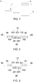
- the semi-transparent film 2 is configured between two shading areas 1 in the conventional mask plate.
- the two shading areas 1 are completely opaque, and thus the photoresist 3 with respect to the two shading areas 1 may be reserved. And only the part of the light may pass through the semi-transparent film 2, thus the photoresist 3 with respect to the semi-transparent film 2 may be partially exposed.
- the remaining photoresist with respect to the semi-transparent film 2 is completely ashed. And a channel of the TFT is obtained corresponding to the semi-transparent film 2 after a series of processes.
- the manufacturing process of the TFT adopting the conventional mask plate may require longer time for conducting the exposure process and the ashing process, which may result in lower productivity and greater power-consuming.
- the present disclosure relates to a mask plate and a manufacturing method of an array substrate configured to reduce the time for conducting the exposure process and the ashing process, so as to reduce power-consuming.
- an array substrate including:
- the first area in the mask plate of the present disclosure is configured to be the semi-transparent area and is configured with the at least two first sub-area spaced apart from each other.
- the thickness of the exposed photoresist on the second sub-area is greater than the thickness of the exposed photoresist on the first sub-area.
- the photoresist corresponding to the second sub-area may be exposed deeper under the same exposure amount when being compared with the conventional exposure process. As such, the present disclosure may reduce the time and the power for the exposure process.
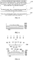
- the present disclosure relates to a mask plate, including: a first area 10, a second area 20, a third area 30, a fourth area 40, a fifth area 50, and a sixth area 60.
- the first area 10 is configured with at least two first sub-areas 101, wherein the first sub-areas 101 are spaced apart from each other, and at least one gap 102 are configured between the first sub-areas 101.
- the first area 10 may include three first sub-areas 101, but is not limited. In another example, the first area may include two, three, or even more first sub-areas.
- the first sub-areas 101 are configured to be semi-transparent areas, and thus only a portion of the light beams may pass through the first sub-areas 101, the remaining portions of the light beams may be reflected.
- the first sub-areas 101 may be made of semi-transparent film.
- the second area 20 is configured with at least one second sub-area 201, wherein the second sub-area 201 is configured in the gap 102 between the first sub-areas 101.
- the first area 10 may include three first sub-areas 101, and the second area 20 may include two second sub-areas 201.
- a transmittance rate of the second sub-area 201 is greater than the first sub-area 101.
- a thickness of the exposed photoresist via the second sub-area 201 is greater than a thickness of the exposed photoresist via the first sub-areas 101.
- a thickness of the remaining photoresist of the second sub-area 201 is less than a thickness of the remaining photoresist of the first sub-areas 101 after a development process.
- An ashing process is conducted on the remaining photoresist, and the ashing process may be terminated upon the photoresist corresponding to the second sub-area is completely ashed.
- at least one channel may be formed on the array substrate corresponding to the at least one second sub-area 201 after conducting an etching process.
- a width of the second sub-area 201 is less than a resolution of an exposure machine, for example less than 2.5mm, of an exposure machine so as to guarantee the channel may be formed on the array substrate corresponding to the second sub-area, so that a diffraction effect may occur and the subsequent process may be completed.
- the exposed photoresist via the second sub-area 201 corresponds to the second sub-area 201 when conducting the exposure process on the photoresist.
- the channel of the array substrate may correspond to the second sub-area 201 after a series manufacturing process, wherein the width of the channel is configured to be the width of the photoresist.
- the width of the channel is configured to be a width of a gap between two shading areas 1.
- the present disclosure adopts the mask plate to reduce the width of the channel and to improve charging rate.
- the second area 20 may include one or two second sub-areas 201.
- the mask plate may include the third area 30, the fourth area 40, the fifth area 50, and the sixth area 60.
- the third area 30 and the fourth area 40 are respectively configured next to two sides of the first area 10.
- the third area 30 and the fourth area 40 may be in the same plane with the first area 10, as shown in FIG. 2 , and may not be in the same plane with the first area 10, as shown in FIG. 3 .
- the third area 30 and the fourth area 40 are configured to be the shading areas 40.
- the first area 10 may be configured below the third area 30 and the fourth area 40.
- the first area 10 may be configured on the third area 30 and the fourth area 40.
- the fifth area 50 and the sixth area 60 are respectively configured next to one side of the third area 30 and one side of the fourth area 40, wherein the side of the third area 30 and the side of the fourth area 40 are facing away the first area 10, and the fifth area 50 and the sixth area 60 are configured to be full translucent areas.
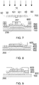
- the present disclosure further relates to a manufacturing process of the array substrates, including the following steps.
- S100 providing a substrate and forming a gate layer, an insulation layer covering the gate layer and the substrate, a semiconductor layer covering the insulation layer, a second metal layer covering the semiconductor layer, and a photoresist layer covering the second metal layer on the substrate in sequence.
- the gate layer 200, the insulation layer 300 covering the gate layer 200 and the substrate 100, the semiconductor layer 400 covering the insulation layer 300, the second metal layer 500 covering the semiconductor layer 400, and the photoresist layer 600 covering the second metal layer 500 are formed on the substrate 100 in sequence.
- the step of forming the gate layer 200 further includes: forming a first metal layer (not shown) on the substrate 100, and conducting a patterned process on the first metal layer to form the gate layer 200.
- the exposure process is to transfer patters of the mask plate 700 onto the photoresist 600 by exposing the ultraviolet (UV).
- UV ultraviolet
- the photoresist layer 600 may be divided into a first exposure area 601 and a second exposure area 602, wherein the first exposure area 601 corresponds to the at least two first sub-areas 101 of the mask plate 700, and the second exposure area 602 corresponds to the at least one second sub-area 201.
- the transmittance rate of the second sub-area 201 is greater than the first sub-area 101, and thus when conducting the exposure process on the photoresist, a thickness of the exposed second exposure area 602 is greater than a thickness of the exposed first exposure area. Due to the first sub-area 101 is configured to be the semi-transparent area, the transmittance rate of a non-hollowed area of the second sub-area 201 is greater than the first sub-area 101, and the width of the hollowed area of the second sub-area 201 is less than the resolution of the exposure machine, the photoresist of the photoresist layer 600 corresponding to the first sub-area 101 and the second sub-area 102 is partially exposed when conducting the exposure process.
- the present disclosure may only expose the photoresist corresponding to the at least two second sub-area 201 to the required thickness, and the photoresist corresponding to the second sub-area 201 may be exposed deeper under the same exposure amount when being compared with the conventional exposure process. As such, the present disclosure may reduce the time and the power for the exposure process and may improve the productivity.
- the mask plate 700 may include the third area 30, the fourth area 40, the fifth area 50, and the sixth area 60.
- the photoresist layer may further include a third exposure area 603 and a fourth exposure area 604.
- the third exposure area 603 corresponds to the third area 30 and fourth area 40 of the mask plate 700
- the fourth area 604 corresponds to the fifth area 50 and the sixth area 60 of the mask plate 700.
- the third area 30 and the fourth area 40 are configured to be the shading areas, and thus the photoresist corresponding to the third exposure area 603 is partially exposed.
- the fifth area 50 and the sixth area 60 are configured to be the full-transparent areas, and thus the photoresist layer 600 corresponding to the fourth exposure area 604 is completely exposed.
- the manufacturing method may further include the following steps.
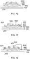
- a first etching process is conducted to remove a first portion of the second metal layer 500 and the semiconductor layer 400, wherein the portion of the second metal layer 500 and the semiconductor layer 400 are not covered by the photoresist layer 600.
- the thickness of the remaining photoresist corresponding to the second sub-area 201 is less than the thickness of the remaining photoresist corresponding to the first sub-area 101.
- the ashing process is conducted on the whole of the remaining photoresist on the semi-transparent film 2. Therefore, the present disclosure may reduce time and power for conducting the ashing process and may improve productivity when being compared with the conventional manufacturing method.
- a second etching process is conducted to remove a second portion of the second metal layer 500 and the semiconductor layer 400, so as to form a source 501 and a drain 502, wherein the second portion of the second metal layer 500 and the semiconductor layer 400 are not covered by the photoresist layer 600.
- the at least one channel 503 is formed on the array substrate corresponding to the at least one second sub-area 201.
- the first area in the mask plate of the present disclosure is configured to be the semi-transparent area and is configured with the at least two first sub-area spaced apart from each other.
- the thickness of the exposed photoresist on the second sub-area is greater than the thickness of the exposed photoresist on the first sub-area.
- the photoresist corresponding to the second sub-area may be exposed deeper under the same exposure amount when being compared with the conventional exposure process. As such, the present disclosure may reduce the time and power for the exposure process.
- the present disclosure may terminate the ashing process upon the photoresist corresponding to the second sub-area is completely ashed, and the thickness of the exposed photoresist corresponding to the second sub-area is less than the exposed photoresist corresponding to the first sub-area.
- the thickness of the remaining photoresist corresponding to the second sub-area is less than the thickness of the remaining photoresist corresponding to the first sub-area.
Landscapes
- Physics & Mathematics (AREA)
- General Physics & Mathematics (AREA)
- Health & Medical Sciences (AREA)
- Engineering & Computer Science (AREA)
- Nonlinear Science (AREA)
- Toxicology (AREA)
- Environmental & Geological Engineering (AREA)
- Epidemiology (AREA)
- Public Health (AREA)
- Crystallography & Structural Chemistry (AREA)
- Optics & Photonics (AREA)
- Chemical & Material Sciences (AREA)
- Manufacturing & Machinery (AREA)
- Preparing Plates And Mask In Photomechanical Process (AREA)
- Exposure And Positioning Against Photoresist Photosensitive Materials (AREA)
- Liquid Crystal (AREA)
- Thin Film Transistor (AREA)
Applications Claiming Priority (2)
| Application Number | Priority Date | Filing Date | Title |
|---|---|---|---|
| CN201710325080.1A CN107132724B (zh) | 2017-05-10 | 2017-05-10 | 一种掩膜版以及阵列基板的制备方法 |
| PCT/CN2017/088614 WO2018205345A1 (zh) | 2017-05-10 | 2017-06-16 | 一种掩膜板以及阵列基板的制备方法 |
Publications (2)
| Publication Number | Publication Date |
|---|---|
| EP3640976A1 true EP3640976A1 (de) | 2020-04-22 |
| EP3640976A4 EP3640976A4 (de) | 2021-03-03 |
Family
ID=59732781
Family Applications (1)
| Application Number | Title | Priority Date | Filing Date |
|---|---|---|---|
| EP17908931.3A Withdrawn EP3640976A4 (de) | 2017-05-10 | 2017-06-16 | Maske und verfahren zur herstellung eines arraysubstrats |
Country Status (6)
| Country | Link |
|---|---|
| US (1) | US10345697B2 (de) |
| EP (1) | EP3640976A4 (de) |
| JP (1) | JP6895525B2 (de) |
| KR (1) | KR102316173B1 (de) |
| CN (1) | CN107132724B (de) |
| WO (1) | WO2018205345A1 (de) |
Cited By (1)
| Publication number | Priority date | Publication date | Assignee | Title |
|---|---|---|---|---|
| US12317593B2 (en) | 2020-02-26 | 2025-05-27 | Fuzhou Boe Optoelectronics Technology Co., Ltd. | Array substrate and display panel having array substrate |
Families Citing this family (3)
| Publication number | Priority date | Publication date | Assignee | Title |
|---|---|---|---|---|
| CN109136834B (zh) * | 2018-09-07 | 2021-03-05 | 京东方科技集团股份有限公司 | 一种掩膜版、oled显示基板及其制备方法 |
| CN109343304B (zh) * | 2018-11-21 | 2020-04-14 | 惠科股份有限公司 | 一种用于制作主动开关的光罩和显示面板的制作方法 |
| CN115064635B (zh) * | 2022-06-07 | 2025-05-30 | 广州华星光电技术有限公司 | 基板的侧面走线的制作方法及显示面板 |
Family Cites Families (23)
| Publication number | Priority date | Publication date | Assignee | Title |
|---|---|---|---|---|
| US7241539B2 (en) * | 2002-10-07 | 2007-07-10 | Samsung Electronics Co., Ltd. | Photomasks including shadowing elements therein and related methods and systems |
| JP4009219B2 (ja) * | 2003-04-10 | 2007-11-14 | 松下電器産業株式会社 | フォトマスク、そのフォトマスクを用いたパターン形成方法及びマスクデータ作成方法 |
| KR100616708B1 (ko) * | 2004-04-12 | 2006-08-28 | 엘지.필립스 엘시디 주식회사 | 액정표시장치 어레이 기판 및 그 제조방법 |
| KR101190045B1 (ko) * | 2005-12-21 | 2012-10-12 | 엘지디스플레이 주식회사 | 포토 마스크 및 이를 이용한 액정표시장치용 어레이 기판의제조 방법 |
| KR101255616B1 (ko) * | 2006-07-28 | 2013-04-16 | 삼성디스플레이 주식회사 | 다중톤 광마스크, 이의 제조방법 및 이를 이용한박막트랜지스터 기판의 제조방법 |
| CN101211118A (zh) * | 2006-12-25 | 2008-07-02 | 上海广电Nec液晶显示器有限公司 | 液晶显示装置制造方法以及在此方法中使用的掩模 |
| JP2009063638A (ja) * | 2007-09-04 | 2009-03-26 | Fujitsu Microelectronics Ltd | フォトマスクの製造方法及び半導体装置の製造方法 |
| KR101407306B1 (ko) * | 2007-12-31 | 2014-06-16 | 엘지디스플레이 주식회사 | 마스크 및 이를 이용한 박막 트랜지스터 기판의 제조 방법 |
| CN101546733B (zh) | 2008-03-28 | 2011-07-27 | 北京京东方光电科技有限公司 | Tft-lcd阵列基板和彩膜基板的制造方法 |
| TWI373097B (en) * | 2008-07-09 | 2012-09-21 | Au Optronics Corp | Method for fabricating thin film transistor array substrate |
| KR101237096B1 (ko) * | 2008-08-21 | 2013-02-25 | 엘지디스플레이 주식회사 | 박막 트랜지스터 어레이 기판의 제조방법 |
| JP5595004B2 (ja) * | 2008-10-21 | 2014-09-24 | 株式会社半導体エネルギー研究所 | 表示装置 |
| CN101738846B (zh) | 2008-11-17 | 2012-02-29 | 北京京东方光电科技有限公司 | 掩模板及其制备方法 |
| KR101079161B1 (ko) * | 2008-12-22 | 2011-11-02 | 엘지이노텍 주식회사 | 하프톤 마스크 및 그 제조방법 |
| TWI444758B (zh) * | 2009-06-19 | 2014-07-11 | Au Optronics Corp | 薄膜電晶體元件與用於定義薄膜電晶體元件之光罩及薄膜電晶體元件之製作方法 |
| CN101615594A (zh) * | 2009-08-14 | 2009-12-30 | 上海广电光电子有限公司 | 薄膜晶体管阵列基板的制造方法 |
| JP5123349B2 (ja) * | 2010-04-19 | 2013-01-23 | Hoya株式会社 | 多階調マスクの製造方法 |
| JP5917020B2 (ja) * | 2010-06-29 | 2016-05-11 | Hoya株式会社 | マスクブランクおよび多階調マスクの製造方法 |
| TWI424507B (zh) * | 2011-04-15 | 2014-01-21 | Chunghwa Picture Tubes Ltd | 薄膜電晶體陣列基板的製造方法 |
| KR101425064B1 (ko) * | 2011-06-09 | 2014-08-01 | 엘지디스플레이 주식회사 | 산화물 박막 트랜지스터 및 그 제조방법 |
| CN102707575B (zh) * | 2012-05-18 | 2015-02-25 | 北京京东方光电科技有限公司 | 掩模板及制造阵列基板的方法 |
| CN103165471A (zh) * | 2013-02-19 | 2013-06-19 | 京东方科技集团股份有限公司 | 薄膜晶体管及其制作方法和显示装置 |
| KR20170035408A (ko) * | 2015-09-22 | 2017-03-31 | 삼성디스플레이 주식회사 | 박막 트랜지스터 표시판 및 그 제조 방법 |
-
2017
- 2017-05-10 CN CN201710325080.1A patent/CN107132724B/zh active Active
- 2017-06-16 KR KR1020197035836A patent/KR102316173B1/ko active Active
- 2017-06-16 JP JP2019538607A patent/JP6895525B2/ja active Active
- 2017-06-16 WO PCT/CN2017/088614 patent/WO2018205345A1/zh not_active Ceased
- 2017-06-16 US US15/541,681 patent/US10345697B2/en active Active
- 2017-06-16 EP EP17908931.3A patent/EP3640976A4/de not_active Withdrawn
Cited By (1)
| Publication number | Priority date | Publication date | Assignee | Title |
|---|---|---|---|---|
| US12317593B2 (en) | 2020-02-26 | 2025-05-27 | Fuzhou Boe Optoelectronics Technology Co., Ltd. | Array substrate and display panel having array substrate |
Also Published As
| Publication number | Publication date |
|---|---|
| JP6895525B2 (ja) | 2021-06-30 |
| US20180329287A1 (en) | 2018-11-15 |
| US10345697B2 (en) | 2019-07-09 |
| KR102316173B1 (ko) | 2021-10-26 |
| EP3640976A4 (de) | 2021-03-03 |
| CN107132724B (zh) | 2019-11-26 |
| KR20200003180A (ko) | 2020-01-08 |
| CN107132724A (zh) | 2017-09-05 |
| JP2020505639A (ja) | 2020-02-20 |
| WO2018205345A1 (zh) | 2018-11-15 |
Similar Documents
| Publication | Publication Date | Title |
|---|---|---|
| TWI674662B (zh) | 陣列基板的製造方法 | |
| US9698171B2 (en) | Array substrate and method of manufacturing the same, and display device | |
| US8134158B2 (en) | TFT-LCD pixel unit and method for manufacturing the same | |
| US6479398B1 (en) | Method of manufacturing an amorphous-silicon thin film transistor | |
| EP2530720B1 (de) | Herstellungsverfahren eines Dünnfilmtransistors und Arraysubstrat und Maske | |
| CN106206456B (zh) | 一种阵列基板的制作方法、阵列基板及显示装置 | |
| CN103165529B (zh) | 一种阵列基板的制备方法 | |
| CN102148259A (zh) | 薄膜晶体管、阵列基板及其制造方法和液晶显示器 | |
| CN105742240B (zh) | 一种ltps阵列基板的制造方法 | |
| WO2020073474A1 (zh) | Tft阵列基板的制作方法 | |
| EP3640976A1 (de) | Maske und verfahren zur herstellung eines arraysubstrats | |
| CN102629608B (zh) | 一种阵列基板及其制造方法和显示装置 | |
| CN103346159B (zh) | 一种阵列基板及其制造方法、显示装置 | |
| US6391499B1 (en) | Light exposure mask and method of manufacturing the same | |
| TWI578546B (zh) | 薄膜電晶體的製造方法 | |
| CN103035652A (zh) | 边缘电场切换型液晶显示板的阵列基底以及其制造方法 | |
| TWI424507B (zh) | 薄膜電晶體陣列基板的製造方法 | |
| JP2004014622A (ja) | 薄膜半導体装置の製造方法及びそのレジストパターン形成方法 | |
| WO2020073547A1 (zh) | 薄膜晶体管及其制造方法 | |
| TWI396916B (zh) | 薄膜電晶體陣列基板之製作方法 | |
| CN110047738B (zh) | 掩膜版、薄膜晶体管和阵列基板及制作方法、显示装置 | |
| KR101577234B1 (ko) | 패턴 형성 방법 및 박막 트랜지스터 어레이 기판의 제조 방법 | |
| CN102830531B (zh) | Tft阵列基板、制造方法及液晶显示装置 | |
| JP3071964B2 (ja) | 液晶表示装置の製造方法 | |
| TWI766198B (zh) | 顯示面板及其製造方法 |
Legal Events
| Date | Code | Title | Description |
|---|---|---|---|
| STAA | Information on the status of an ep patent application or granted ep patent |
Free format text: STATUS: THE INTERNATIONAL PUBLICATION HAS BEEN MADE |
|
| PUAI | Public reference made under article 153(3) epc to a published international application that has entered the european phase |
Free format text: ORIGINAL CODE: 0009012 |
|
| STAA | Information on the status of an ep patent application or granted ep patent |
Free format text: STATUS: REQUEST FOR EXAMINATION WAS MADE |
|
| 17P | Request for examination filed |
Effective date: 20191128 |
|
| AK | Designated contracting states |
Kind code of ref document: A1 Designated state(s): AL AT BE BG CH CY CZ DE DK EE ES FI FR GB GR HR HU IE IS IT LI LT LU LV MC MK MT NL NO PL PT RO RS SE SI SK SM TR |
|
| AX | Request for extension of the european patent |
Extension state: BA ME |
|
| DAV | Request for validation of the european patent (deleted) | ||
| DAX | Request for extension of the european patent (deleted) | ||
| A4 | Supplementary search report drawn up and despatched |
Effective date: 20210129 |
|
| RIC1 | Information provided on ipc code assigned before grant |
Ipc: G03F 1/54 20120101ALI20210125BHEP Ipc: G03F 1/50 20120101ALI20210125BHEP Ipc: H01L 21/77 20170101AFI20210125BHEP Ipc: H01L 27/12 20060101ALI20210125BHEP |
|
| STAA | Information on the status of an ep patent application or granted ep patent |
Free format text: STATUS: EXAMINATION IS IN PROGRESS |
|
| 17Q | First examination report despatched |
Effective date: 20230605 |
|
| GRAP | Despatch of communication of intention to grant a patent |
Free format text: ORIGINAL CODE: EPIDOSNIGR1 |
|
| STAA | Information on the status of an ep patent application or granted ep patent |
Free format text: STATUS: GRANT OF PATENT IS INTENDED |
|
| INTG | Intention to grant announced |
Effective date: 20231023 |
|
| STAA | Information on the status of an ep patent application or granted ep patent |
Free format text: STATUS: THE APPLICATION IS DEEMED TO BE WITHDRAWN |
|
| 18D | Application deemed to be withdrawn |
Effective date: 20240305 |