EP3633807B1 - Lichtemittierendes element und herstellungsverfahren für lichtemittierendes element - Google Patents
Lichtemittierendes element und herstellungsverfahren für lichtemittierendes element Download PDFInfo
- Publication number
- EP3633807B1 EP3633807B1 EP18810741.1A EP18810741A EP3633807B1 EP 3633807 B1 EP3633807 B1 EP 3633807B1 EP 18810741 A EP18810741 A EP 18810741A EP 3633807 B1 EP3633807 B1 EP 3633807B1
- Authority
- EP
- European Patent Office
- Prior art keywords
- convex portion
- layer
- resist
- convex
- light
- Prior art date
- Legal status (The legal status is an assumption and is not a legal conclusion. Google has not performed a legal analysis and makes no representation as to the accuracy of the status listed.)
- Active
Links
- 238000004519 manufacturing process Methods 0.000 title claims description 48
- 239000000758 substrate Substances 0.000 claims description 113
- 230000015572 biosynthetic process Effects 0.000 claims description 55
- 239000004065 semiconductor Substances 0.000 claims description 47
- 238000000034 method Methods 0.000 claims description 44
- 229910052751 metal Inorganic materials 0.000 claims description 29
- 239000002184 metal Substances 0.000 claims description 29
- VYPSYNLAJGMNEJ-UHFFFAOYSA-N silicon dioxide Inorganic materials O=[Si]=O VYPSYNLAJGMNEJ-UHFFFAOYSA-N 0.000 claims description 16
- 238000001312 dry etching Methods 0.000 claims description 13
- 229910052681 coesite Inorganic materials 0.000 claims description 9
- 229910052906 cristobalite Inorganic materials 0.000 claims description 9
- 229910052682 stishovite Inorganic materials 0.000 claims description 9
- 229910052905 tridymite Inorganic materials 0.000 claims description 9
- JMASRVWKEDWRBT-UHFFFAOYSA-N Gallium nitride Chemical compound [Ga]#N JMASRVWKEDWRBT-UHFFFAOYSA-N 0.000 claims description 6
- 238000007493 shaping process Methods 0.000 claims 2
- 230000004048 modification Effects 0.000 description 37
- 238000012986 modification Methods 0.000 description 37
- 238000005530 etching Methods 0.000 description 24
- 238000010586 diagram Methods 0.000 description 21
- 238000013461 design Methods 0.000 description 13
- 230000000694 effects Effects 0.000 description 12
- 230000008569 process Effects 0.000 description 8
- 238000007740 vapor deposition Methods 0.000 description 8
- 229910052737 gold Inorganic materials 0.000 description 7
- 239000000377 silicon dioxide Substances 0.000 description 7
- 238000005229 chemical vapour deposition Methods 0.000 description 6
- 230000003287 optical effect Effects 0.000 description 6
- 230000010355 oscillation Effects 0.000 description 6
- 229910002601 GaN Inorganic materials 0.000 description 5
- MCMNRKCIXSYSNV-UHFFFAOYSA-N Zirconium dioxide Chemical compound O=[Zr]=O MCMNRKCIXSYSNV-UHFFFAOYSA-N 0.000 description 4
- 239000012535 impurity Substances 0.000 description 4
- ZKATWMILCYLAPD-UHFFFAOYSA-N niobium pentoxide Chemical compound O=[Nb](=O)O[Nb](=O)=O ZKATWMILCYLAPD-UHFFFAOYSA-N 0.000 description 4
- 239000004020 conductor Substances 0.000 description 3
- 239000000463 material Substances 0.000 description 3
- 238000005498 polishing Methods 0.000 description 3
- 229910002704 AlGaN Inorganic materials 0.000 description 2
- GWEVSGVZZGPLCZ-UHFFFAOYSA-N Titan oxide Chemical compound O=[Ti]=O GWEVSGVZZGPLCZ-UHFFFAOYSA-N 0.000 description 2
- 230000004888 barrier function Effects 0.000 description 2
- 239000013078 crystal Substances 0.000 description 2
- 238000002347 injection Methods 0.000 description 2
- 239000007924 injection Substances 0.000 description 2
- 239000011777 magnesium Substances 0.000 description 2
- 238000001020 plasma etching Methods 0.000 description 2
- 229910000679 solder Inorganic materials 0.000 description 2
- PBCFLUZVCVVTBY-UHFFFAOYSA-N tantalum pentoxide Inorganic materials O=[Ta](=O)O[Ta](=O)=O PBCFLUZVCVVTBY-UHFFFAOYSA-N 0.000 description 2
- 238000001039 wet etching Methods 0.000 description 2
- 229910001218 Gallium arsenide Inorganic materials 0.000 description 1
- ATUUNJCZCOMUKD-OKILXGFUSA-N MLI-2 Chemical compound C1[C@@H](C)O[C@@H](C)CN1C1=CC(C=2C3=CC(OC4(C)CC4)=CC=C3NN=2)=NC=N1 ATUUNJCZCOMUKD-OKILXGFUSA-N 0.000 description 1
- FYYHWMGAXLPEAU-UHFFFAOYSA-N Magnesium Chemical compound [Mg] FYYHWMGAXLPEAU-UHFFFAOYSA-N 0.000 description 1
- CPLXHLVBOLITMK-UHFFFAOYSA-N Magnesium oxide Chemical compound [Mg]=O CPLXHLVBOLITMK-UHFFFAOYSA-N 0.000 description 1
- XUIMIQQOPSSXEZ-UHFFFAOYSA-N Silicon Chemical compound [Si] XUIMIQQOPSSXEZ-UHFFFAOYSA-N 0.000 description 1
- 230000004075 alteration Effects 0.000 description 1
- PNEYBMLMFCGWSK-UHFFFAOYSA-N aluminium oxide Inorganic materials [O-2].[O-2].[O-2].[Al+3].[Al+3] PNEYBMLMFCGWSK-UHFFFAOYSA-N 0.000 description 1
- 229910052593 corundum Inorganic materials 0.000 description 1
- 230000008878 coupling Effects 0.000 description 1
- 238000010168 coupling process Methods 0.000 description 1
- 238000005859 coupling reaction Methods 0.000 description 1
- 238000002109 crystal growth method Methods 0.000 description 1
- 238000009795 derivation Methods 0.000 description 1
- 238000005516 engineering process Methods 0.000 description 1
- 230000005484 gravity Effects 0.000 description 1
- AMGQUBHHOARCQH-UHFFFAOYSA-N indium;oxotin Chemical compound [In].[Sn]=O AMGQUBHHOARCQH-UHFFFAOYSA-N 0.000 description 1
- 229910010272 inorganic material Inorganic materials 0.000 description 1
- 239000011147 inorganic material Substances 0.000 description 1
- 238000005468 ion implantation Methods 0.000 description 1
- 229910052749 magnesium Inorganic materials 0.000 description 1
- 229910052759 nickel Inorganic materials 0.000 description 1
- 150000004767 nitrides Chemical class 0.000 description 1
- 125000002524 organometallic group Chemical group 0.000 description 1
- 230000001590 oxidative effect Effects 0.000 description 1
- 238000012545 processing Methods 0.000 description 1
- 230000006798 recombination Effects 0.000 description 1
- 238000005215 recombination Methods 0.000 description 1
- 230000007261 regionalization Effects 0.000 description 1
- 229910052710 silicon Inorganic materials 0.000 description 1
- 239000010703 silicon Substances 0.000 description 1
- 235000012239 silicon dioxide Nutrition 0.000 description 1
- 239000000243 solution Substances 0.000 description 1
- 239000000126 substance Substances 0.000 description 1
- JBQYATWDVHIOAR-UHFFFAOYSA-N tellanylidenegermanium Chemical compound [Te]=[Ge] JBQYATWDVHIOAR-UHFFFAOYSA-N 0.000 description 1
- 238000013519 translation Methods 0.000 description 1
- 238000001947 vapour-phase growth Methods 0.000 description 1
- 229910001845 yogo sapphire Inorganic materials 0.000 description 1
Images


Classifications
-
- H—ELECTRICITY
- H01—ELECTRIC ELEMENTS
- H01S—DEVICES USING THE PROCESS OF LIGHT AMPLIFICATION BY STIMULATED EMISSION OF RADIATION [LASER] TO AMPLIFY OR GENERATE LIGHT; DEVICES USING STIMULATED EMISSION OF ELECTROMAGNETIC RADIATION IN WAVE RANGES OTHER THAN OPTICAL
- H01S5/00—Semiconductor lasers
- H01S5/10—Construction or shape of the optical resonator, e.g. extended or external cavity, coupled cavities, bent-guide, varying width, thickness or composition of the active region
- H01S5/18—Surface-emitting [SE] lasers, e.g. having both horizontal and vertical cavities
- H01S5/183—Surface-emitting [SE] lasers, e.g. having both horizontal and vertical cavities having only vertical cavities, e.g. vertical cavity surface-emitting lasers [VCSEL]
- H01S5/18305—Surface-emitting [SE] lasers, e.g. having both horizontal and vertical cavities having only vertical cavities, e.g. vertical cavity surface-emitting lasers [VCSEL] with emission through the substrate, i.e. bottom emission
-
- H—ELECTRICITY
- H01—ELECTRIC ELEMENTS
- H01S—DEVICES USING THE PROCESS OF LIGHT AMPLIFICATION BY STIMULATED EMISSION OF RADIATION [LASER] TO AMPLIFY OR GENERATE LIGHT; DEVICES USING STIMULATED EMISSION OF ELECTROMAGNETIC RADIATION IN WAVE RANGES OTHER THAN OPTICAL
- H01S5/00—Semiconductor lasers
- H01S5/10—Construction or shape of the optical resonator, e.g. extended or external cavity, coupled cavities, bent-guide, varying width, thickness or composition of the active region
- H01S5/18—Surface-emitting [SE] lasers, e.g. having both horizontal and vertical cavities
- H01S5/183—Surface-emitting [SE] lasers, e.g. having both horizontal and vertical cavities having only vertical cavities, e.g. vertical cavity surface-emitting lasers [VCSEL]
- H01S5/18361—Structure of the reflectors, e.g. hybrid mirrors
- H01S5/18375—Structure of the reflectors, e.g. hybrid mirrors based on metal reflectors
-
- H—ELECTRICITY
- H01—ELECTRIC ELEMENTS
- H01S—DEVICES USING THE PROCESS OF LIGHT AMPLIFICATION BY STIMULATED EMISSION OF RADIATION [LASER] TO AMPLIFY OR GENERATE LIGHT; DEVICES USING STIMULATED EMISSION OF ELECTROMAGNETIC RADIATION IN WAVE RANGES OTHER THAN OPTICAL
- H01S5/00—Semiconductor lasers
- H01S5/02—Structural details or components not essential to laser action
- H01S5/0206—Substrates, e.g. growth, shape, material, removal or bonding
- H01S5/0207—Substrates having a special shape
-
- H—ELECTRICITY
- H01—ELECTRIC ELEMENTS
- H01S—DEVICES USING THE PROCESS OF LIGHT AMPLIFICATION BY STIMULATED EMISSION OF RADIATION [LASER] TO AMPLIFY OR GENERATE LIGHT; DEVICES USING STIMULATED EMISSION OF ELECTROMAGNETIC RADIATION IN WAVE RANGES OTHER THAN OPTICAL
- H01S5/00—Semiconductor lasers
- H01S5/02—Structural details or components not essential to laser action
- H01S5/022—Mountings; Housings
- H01S5/0235—Method for mounting laser chips
- H01S5/02355—Fixing laser chips on mounts
-
- H—ELECTRICITY
- H01—ELECTRIC ELEMENTS
- H01S—DEVICES USING THE PROCESS OF LIGHT AMPLIFICATION BY STIMULATED EMISSION OF RADIATION [LASER] TO AMPLIFY OR GENERATE LIGHT; DEVICES USING STIMULATED EMISSION OF ELECTROMAGNETIC RADIATION IN WAVE RANGES OTHER THAN OPTICAL
- H01S5/00—Semiconductor lasers
- H01S5/02—Structural details or components not essential to laser action
- H01S5/022—Mountings; Housings
- H01S5/0235—Method for mounting laser chips
- H01S5/02375—Positioning of the laser chips
-
- H—ELECTRICITY
- H01—ELECTRIC ELEMENTS
- H01S—DEVICES USING THE PROCESS OF LIGHT AMPLIFICATION BY STIMULATED EMISSION OF RADIATION [LASER] TO AMPLIFY OR GENERATE LIGHT; DEVICES USING STIMULATED EMISSION OF ELECTROMAGNETIC RADIATION IN WAVE RANGES OTHER THAN OPTICAL
- H01S5/00—Semiconductor lasers
- H01S5/10—Construction or shape of the optical resonator, e.g. extended or external cavity, coupled cavities, bent-guide, varying width, thickness or composition of the active region
- H01S5/18—Surface-emitting [SE] lasers, e.g. having both horizontal and vertical cavities
- H01S5/183—Surface-emitting [SE] lasers, e.g. having both horizontal and vertical cavities having only vertical cavities, e.g. vertical cavity surface-emitting lasers [VCSEL]
- H01S5/18308—Surface-emitting [SE] lasers, e.g. having both horizontal and vertical cavities having only vertical cavities, e.g. vertical cavity surface-emitting lasers [VCSEL] having a special structure for lateral current or light confinement
- H01S5/18322—Position of the structure
- H01S5/18327—Structure being part of a DBR
-
- H—ELECTRICITY
- H01—ELECTRIC ELEMENTS
- H01S—DEVICES USING THE PROCESS OF LIGHT AMPLIFICATION BY STIMULATED EMISSION OF RADIATION [LASER] TO AMPLIFY OR GENERATE LIGHT; DEVICES USING STIMULATED EMISSION OF ELECTROMAGNETIC RADIATION IN WAVE RANGES OTHER THAN OPTICAL
- H01S5/00—Semiconductor lasers
- H01S5/10—Construction or shape of the optical resonator, e.g. extended or external cavity, coupled cavities, bent-guide, varying width, thickness or composition of the active region
- H01S5/18—Surface-emitting [SE] lasers, e.g. having both horizontal and vertical cavities
- H01S5/183—Surface-emitting [SE] lasers, e.g. having both horizontal and vertical cavities having only vertical cavities, e.g. vertical cavity surface-emitting lasers [VCSEL]
- H01S5/18386—Details of the emission surface for influencing the near- or far-field, e.g. a grating on the surface
- H01S5/18388—Lenses
Definitions
- the present disclosure relates to a light-emitting device and a method of manufacturing a light- emitting device.
- a technology has been disclosed that shapes a reflecting mirror of a surface-emitting laser into a concave curve.
- a reflecting mirror of a surface-emitting laser is made concave-curve-shaped, it is requested to not only dispose an optical axis of the surface-emitting laser at a predetermined position with respect to a wiring substrate, but also protect the reflecting mirror having a concave-curved shape. Therefore, it is desirable to provide a light-emitting device that allows for alignment with respect to the wiring substrate and protection of the reflecting mirror having a concave-curved shape, and a method of manufacturing the light-emitting device.
- Embodiments of the present disclosure are defined by the appended Claims.
- the self-alignment function of the convex curve of the second convex portion or the convex curve of the layer formed following the convex curve of the second convex portion makes it possible to determine the mounting position of the light-emitting device and to protect the first convex portion by the second convex portion in the manufacturing process or the mounting process of the light-emitting device. Consequently, it is possible to precisely perform alignment of the light-emitting device with respect to the wiring substrate and to protect the reflecting mirror having a concave-curved shape.
- the effects of the present disclosure are not necessarily limited to the effects described here, but may include any of the effects described herein.
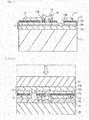
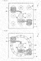
- FIG. 1 illustrates a cross-sectional configuration example of the light-emitting device 1.
- FIG. 2 illustrates a top configuration example of the light-emitting device 1.
- the light-emitting device 1 is a semiconductor laser of upper surface emission type which is preferably applicable to an application that requests a thin and less power consuming semiconductor laser or an application that requests a thin semiconductor laser large in area, etc.
- the light-emitting device 1 includes a vertical resonator.
- the vertical resonator is configured to be oscillated at a predetermined oscillation wavelength ⁇ 0 by two DBRs (distributed Bragg reflector) facing each other in a normal direction of a substrate 11.
- the vertical resonator includes two DBR layers sandwiching the substrate 11, a laminate 12, and an opening 13A of a current constriction layer 13. That is, the substrate 11 is a substrate provided inside the vertical resonator and is the substrate provided between one of the DBR layers and the laminate 12.
- the aforementioned two DBR layers include a DBR layer 18 (first reflecting mirror) on a semiconductor layer 12a side described later and a DBR layer 16 (second reflecting mirror) on a semiconductor layer 12c side described later.
- the DBR layer 18 is formed in contact with a rear surface of the substrate 11.
- the laminate 12 includes, for example, an active layer 12b and two semiconductor layers sandwiching the active layer 12b.
- the aforementioned two semiconductor layers include the semiconductor layer 12a closer to the substrate 11 and the semiconductor layer 12c away from the substrate 11.
- the light-emitting device 1 includes, on the substrate 11, for example, the semiconductor layer 12a, the active layer 12b, the semiconductor layer 12c, the current constriction layer 13, an electrode layer 14, electrode pads 15 and 17, and a DBR layer 16 in this order from the substrate 11 side.
- the light-emitting device 1 further includes, on the rear surface side of the substrate 11, for example, the DBR layer 18 and a metal layer 19 in this order from the substrate 11 side.
- the laminate 12 may also include, on an outermost surface on the semiconductor layer 12c side, for example, a contact layer for causing the semiconductor layer 12c and the electrode layer 14 to come into ohmic contact with each other.
- the contact layer may be a layer formed by doping the outermost surface of the semiconductor layer 12c with impurities in high concentration or may be a layer that is formed separately from the semiconductor layer 12c and is in contact with the outermost surface of the semiconductor layer 12c.
- the substrate 11 is a crystal growth substrate used at the time of epitaxial crystal growth of the laminate 12.
- the substrate 11 and the laminate 12 include a gallium-nitride based semiconductor.
- the substrate 11 is an optically transparent substrate and is a GaN substrate, for example.
- the laminate 12 includes GaN, AlGaN, AlInN, GaInN, AlGaInN, etc., for example.
- the semiconductor layer 12a includes GaN, for example.
- the semiconductor layer 12a includes silicon (Si), etc., for example, as an n-type impurity. That is, the semiconductor layer 12a is an n-type semiconductor layer.
- the semiconductor layer 12c includes GaN, for example.
- the semiconductor layer 12c includes magnesium (Mg) or zinc (Zn), etc., for example, as a p-type impurity. That is, the semiconductor layer 12c is a p-type semiconductor layer.
- the active layer 12b has a quantum well structure, for example. Examples of types of the quantum well structures include a single quantum well structure (QW structure) or a multiple quantum well structure (MQW structure).
- the quantum well structure has a structure in which well layers and barrier layers are alternately stacked.
- Examples of combinations of the well layer and the barrier layer include (In y Ga (1-y) N, GaN), (In y Ga (1-y) N, In z Ga (1-z) N) [where y > z], or (In y Ga (1-y) N, AlGaN), etc.
- the current constriction layer 13 is a layer for constricting an electric current to be injected into the active layer 12b.
- the current constriction layer 13 includes an insulating layer having the opening 13A, for example.
- the insulating layer is formed in contact with the outermost surface of the laminate 12, for example, and includes an inorganic material such as SiO2, for example. It is to be noted that the insulating layer may also include a high-resistance region formed by injection of impurities from the semiconductor layer 12c side of the laminate 12 into the laminate 12.
- the light-emitting device 1 may include a layer having a function equivalent to the function of the current constriction layer 13, instead of the current constriction layer 13.
- the light-emitting device 1 may also include a contact layer, for example, between the semiconductor layer 12c and the electrode layer 14.
- the contact layer has a size equivalent to the size of the opening 13A.
- Such a contact layer is formed by formation of the contact layer over a whole surface of the semiconductor layer 12c, for example, and then selective etching by RIE (Reactive Ion Etching) method, etc. Provision of such a contact layer also makes it possible to perform current constriction.
- the light-emitting device 1 may also have an annular oxidized region.
- the annular oxidized region is formed by dry etching with a portion of the laminate 12, which serves as a light-emitting unit 10, for example, masked to form the laminate 12 into a cylindrical shape, and then partially oxidizing the cylindrical-shaped laminate 12 from a lateral direction. Provision of such an oxidized region also makes it possible to perform current constriction.
- the opening 13A has a circular shape, for example. A diameter of the opening 13A is approximately 10 ⁇ m, for example.
- the electrode layer 14 is in contact with a surface of the laminate 12, which is exposed to a bottom surface of the opening 13A of the current constriction layer 13.
- the electrode layer 14 includes a transparent electrically-conductive material, for example. Examples of the transparent electrically-conductive materials used for the electrode layer 14 include ITO (Indium Tin Oxide), etc.
- the electrode pad 15 is to be electrically coupled to an external electrode or circuit, and electrically coupled to the electrode layer 14.
- the electrode pad 15 is in contact with a portion of the electrode layer 14 not facing the opening 13A, for example.
- the electrode pad 15 includes, for example, Pd/Ti/Pt/Au, Ti/Pd/Au, Ti/Ni/Au, Ni/Au, or the like.
- the electrode pad 17 is to be electrically coupled to an external electrode or circuit, and electrically coupled to the semiconductor layer 12a.
- the current constriction layer 13 has an opening 13B in a region around the vertical resonator.
- the laminate 12 has a groove at a position facing the opening 13B, and the semiconductor layer 12a is exposed to a bottom surface of the groove.
- the electrode pad 17 is in contact with the semiconductor layer 12a via the opening 13B of the current constriction layer 13 and the groove of the laminate 12.
- the electrode pad 17 is in contact with a portion of the semiconductor layer 12c not facing the opening 13A, for example.
- the electrode pad 17 includes, for example, Pd/Ti/Pt/Au, Ti/Pd/Au, Ti/Ni/Au, or the like.
- the electrode pad 17 may also be electrically coupled to the semiconductor layer 12a via another member.
- the electrode pad 17 may be electrically coupled to the semiconductor layer 12a via the substrate 11.
- the electrode pad 17 may also be placed on the rear surface (flat surface 11S to be described later) of the substrate 11.
- the DBR layers 16 and 18 each include a dielectric multi-layer, for example.
- the dielectric multi-layer has a structure in which low refractive index layers and high refractive index layers are alternately stacked.
- the low refractive index layer has a thickness of an odd multiple of ⁇ 0 /4n 1 (n 1 being a refractive index of the low refractive index layer).
- the high refractive index layer has a thickness of an odd multiple of ⁇ 0 /4n 2 (n 2 being a refractive index of the high refractive index layer).
- Examples of materials of the dielectric multi-layers included in the DBR layers 16 and 18 include SiO 2 , SiN Al 2 O 3 , Nb 2 O 5 , Ta 2 O 5 , TiO 2 , A1N, MgO, and ZrO 2 .
- examples of combinations of the low refractive index layer and the high refractive index layer include SiO 2 /SiN, SiO 2 /Nb 2 O 5 , SiO 2 /ZrO 2 , SiO 2 /AlN, SiO 2 /Ta 2 O 5 , etc.
- the dielectric multi-layers included in the DBR layers 16 and 18 are formed by a film formation method such as a sputter, CVD, or vapor deposition, for example.
- the metal layer 19 is formed in contact with a surface of the DBR layer 18, and, for example, is formed in contact with a whole surface of the DBR layer 18.
- the metal layer 19 is formed following the surface of the DBR layer 18.
- the metal layer 19 includes, for example, Pd/Ti/Pt/Au, Ti/Pd/Au, Ti/Ni/Au, or the like. It is to be noted that in a case where an opening is partially provided in the DBR layer 18, the metal layer 19 may also be electrically coupled to the semiconductor layer 12a via the substrate 11 exposed into an opening of the DBR layer 18. In that case, it is possible to cause the metal layer 19 to have a function similar to the electrode pad 17.
- the substrate 11 has a convex portion 11A (first convex portion) protruding to the side opposite to the laminate 12, on the rear surface.
- the convex portion 11A is provided at a position facing the opening 13A.
- a whole surface of the convex portion 11A has a convex-curved shape, protruding to the side opposite to the laminate 12. It is preferable that a radius of curvature of the surface of the convex portion 11A be larger than the resonator length of the vertical resonator.
- the radius of curvature of the surface of the convex portion 11A is less than or equal to the resonator length of the vertical resonator, optical field confinement becomes excessive, which easily causes optical loss.
- the substrate 11 further has a plurality of convex portions 11B (second convex portions) protruding to the side opposite to the laminate 12, on the rear surface.
- the plurality of convex portions 11B is provided avoiding the position facing the opening 13A.
- the plurality of convex portions 11B is provided around the convex portion 11A.
- the plurality of convex portions 11B is disposed at point-symmetric positions about the convex portion 11A, for example.
- Each of the convex portions 11B is island-shaped.
- Each of the convex portions 11B has a circular shape, an elliptical shape, or a polygonal shape, for example, when viewed from the normal direction of the substrate 11.
- the convex portion 11B has the height greater than or equal to the height of the convex portion 11A, and at least a surface of an end on the convex portion 11A side has a convex-curved shape.
- a whole surface of the convex portion 11B may have a convex-curved shape, protruding to the side opposite to the laminate 12.
- the end of the convex portion 11B on the convex portion 11A side has a convex-curved shape, protruding onto the convex portion 11A side.
- the height of the convex portion 11A or 11B refers to a height from the flat surface 11S corresponding to bases of the convex portion 11A and the convex portion 11B on the rear surface of the substrate 11.
- the metal layer 19 is formed following the surface of the DBR layer 18. Consequently, a spot of the metal layer 19 facing the convex portion 11A curves following the surface of the DBR layer 18, and configures a convex portion 10A protruding to the side opposite to the laminate 12. In addition, a spot of the metal layer 19 facing the convex portion 11B also curves following the surface of the DBR layer 18, and configures a convex portion 10B protruding to the side opposite to the laminate 12.
- the convex portion 10B has the height greater than or equal to the height of the convex portion 10A, and a surface of an end on the convex portion 10A side has a convex-curved shape.
- a whole surface of the convex portion 10A has a convex-curved shape, for example, protruding to the side opposite to the laminate 12.
- the height of the convex portion 10A or 10B refers to a height from the flat surface 11S corresponding to bases of the convex portion 11A and the convex portion 11B on the rear surface of the substrate 11.
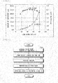
- FIG. 3 illustrates an example of a relation between a lens diameter, a lens height, and a lens radius of curvature.
- the lens diameter refers to the diameter of the convex portion 11A and the diameter of the convex portion 11B.
- the lens height refers to the height of the convex portion 11A and the height of the convex portion 11B.
- the radius of curvature refers to the radius of curvature of the surface of the convex portion 11A and the radius of curvature of the surface of the convex portion 11B.
- the convex portion 11B has a height greater than or equal to the height of the convex portion 11A.
- the height of the convex portion 11A and the height of the convex portion 11B are formed by etching of the substrate 11 with the reflowed island-shaped resist layer as the mask, as described later.
- the diameter of the reflowed island-shaped resist layer corresponds to the lens diameter of FIG. 3 . That is, changing the diameter of the reflowed island-shaped resist layer may make it possible to adjust the heights or the radii of curvature of the convex portion 11A and the convex portion 11B.
- a design is assumed that makes the diameter of the island-shaped resist layer to be used in formation of the convex portion 11B smaller than the diameter of the island-shaped resist layer to be used in formation of the convex portion 11A.
- the diameter of the island-shaped resist layer to be used in the formation of the convex portion 11A is 80 ⁇ m, and the diameter of the island-shaped resist layer to be used in the formation of the convex portion 11B is greater than or equal to 30 ⁇ m and less than or equal to 70 ⁇ m.
- the diameter of the convex portion 11A is 80 ⁇ m
- the diameter of the convex portion 11B is greater than or equal to 30 ⁇ m and less than or equal to 70 ⁇ m
- the radius of curvature of the surface of the convex portion 11B is smaller than the radius of curvature of the convex portion 11A.
- a design is assumed that makes the diameter of the island-shaped resist layer to be used in formation of the convex portion 11B larger than the diameter of the island-shaped resist layer to be used in formation of the convex portion 11A.
- the diameter of the island-shaped resist layer to be used in the formation of the convex portion 11A is 30 ⁇ m
- the diameter of the island-shaped resist layer to be used in the formation of the convex portion 11B is greater than or equal to 40 ⁇ m and less than or equal to 60 ⁇ m.
- the diameter of the convex portion 11A is 30 ⁇ m
- the diameter of the convex portion 11B is greater than or equal to 40 ⁇ m and less than or equal to 60 ⁇ m
- the radius of curvature of the surface of the convex portion 11B is larger than the radius of curvature of the convex portion 11A.
- the DBR layer 18 is formed following at least the surface of the convex portion 11A, and functions as a reflecting mirror having a concave-curved shape for the vertical resonator.
- the DBR layer 18 has a concave-curved shape, curving to the side opposite to the laminate 12.
- the DBR layer 18 may be formed following a whole surface including the surfaces of the convex portions 11A and 11B.
- FIG. 1 illustrates an example of a case where the DBR layer 18 is formed following a whole surface including the surfaces of the convex portions 11A and 11B.
- the DBR layer 16 is formed following a surface of the electrode layer 14, and formed in contact with the surface of the electrode layer 14.
- a portion of the DBR layer 16 facing the opening 13A is substantially flat. It is preferable that the active layer 12b be disposed closer to the DBR layer 16 and the current constriction layer 13 than to the DBR layer 18. One reason for this is that this intensifies the optical field confinement in the active layer 12b, thereby making laser oscillation easier. It is also preferable that the shortest distance D CI from an area center of gravity point of the current constriction layer 13 to an inner edge of the opening 13A satisfy the following expression.
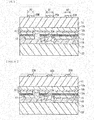
- FIG. 4 illustrates an example of a manufacturing procedure of the light-emitting device 1.
- FIGs. 5 to 13 each illustrate an example of a manufacturing process of the light-emitting device 1.
- the laminate 12 is formed on the surface (first main surface) of the substrate 11 by an epitaxial crystal growth method such as an MOCVD (Metal Organic Chemical Vapor Deposition: organometallic vapor-phase growth) method, for example ( FIG. 5 ).
- MOCVD Metal Organic Chemical Vapor Deposition: organometallic vapor-phase growth
- the current constriction layer 13 having the opening 13A is formed on the surface of the laminate 12 by, for example, a CVD (chemical vapor deposition) method, a sputter method, a vapor deposition method, or ion implantation, etc. ( FIG. 6 ).
- the DBR layer 16 is formed on the electrode layer 14 by, for example, the CVD method, the sputter method, or the vapor deposition method, etc. ( FIG. 6 ).
- an etching method such as a wet etching method or a dry etching method, or a pattern formation method such as a lift-off method is used, for example.
- the electrode pad 15 is formed to be in contact with the end of the electrode layer 14, by the vapor deposition method, for example ( FIG. 7 ). Then, by the wet etching method or the dry etching method, etc., for example, the opening 13B is formed on the current constriction layer 13, and a groove is formed in the laminate 12 until the semiconductor layer 12a is exposed ( FIG. 7 ). Subsequently, by the vapor deposition method, etc., for example, the electrode pad 17 is formed ( FIG. 7 ). At this time, the electrode pad 17 is formed to be in contact with the semiconductor layer 12a via the opening 13B formed in the current constriction layer 13 and the groove formed in the laminate 12.
- a support substrate 22 is pasted to a surface including the electrode pads 15 and 17 via an adhesion layer 21.
- the rear surface (second main surface) of the substrate 11 on the side opposite to the surface (first main surface) is mirror-finished by, for example, etching such as CMP (Chemical Mechanical Polishing) or polishing with a grinder ( FIG. 8 , step S101).
- the substrate 11 has a thickness of 100 ⁇ m or less.
- a resist pattern is formed on the polished rear surface of the substrate 11.
- a resist layer 23A (first resist layer) is formed in the island shape at a spot facing the opening 13A and two or more resist layers 23B (second resist layers) are formed in the island shape around the spot facing the opening 13A ( FIG. 9 , step S102).
- the resist layers 23A and 23B each have, for example, a circular shape, an elliptical shape, or a polygonal shape.
- Width R1 and width R2 of the resist layer 23A and the resist layer 23B differ from each other.
- the width R1 and the width R2 of the resist layer 23A and the resist layer 23B are set by the reflow and the resist etch-back, to be descried later, to cause each of the convex portions 11B to have a height greater than or equal to the height of the convex portion 11A.
- the width R1 and the width R2 of the resist layer 23A and the resist layer 23B are set on the basis of the relation described in FIG. 3 to cause the height of the convex portion 11B to be greater than or equal to the height of the convex portion 11A.
- a design is assumed that makes the diameter of the island-shaped resist layer 23B to be used in formation of the convex portion 11B smaller than the diameter of the island-shaped resist layer 23A to be used in formation of the convex portion 11A.
- the width R1 of the resist layer 23A is 80 ⁇ m
- the width R2 of the resist layer 23B is greater than or equal to 30 ⁇ m and less than or equal to 70 ⁇ m.
- the diameter of the convex portion 11A is 80 ⁇ m
- the diameter of the convex portion 11B is greater than or equal to 30 ⁇ m and less than or equal to 70 ⁇ m
- the radius of curvature of the surface of the convex portion 11B is smaller than the radius of curvature of the convex portion 11A.
- the diameter of the island-shaped resist layer 23B to be used in formation of the convex portion 11B larger than the diameter of the island-shaped resist layer 23A to be used in formation of the convex portion 11A.
- the width R1 of the resist layer 23A is 30 ⁇ m
- the width R2 of the resist layer 23B is greater than or equal to 40 ⁇ m and less than or equal to 60 ⁇ m.
- the diameter of the convex portion 11A is 30 ⁇ m
- the diameter of the convex portion 11B is greater than or equal to 40 ⁇ m and less than or equal to 60 ⁇ m
- the radius of curvature of the surface of the convex portion 11B is larger than the radius of curvature of the convex portion 11A.
- the reflow is performed on the resist layer 23A and the plurality of resist layers 23B ( FIG. 10 , step S103).
- the height of the resist layer 23B is greater than or equal to the height of the resist layer 23A.
- step S104 dry etching is performed on the substrate 11 with the resist layers 23A and 23B, the surfaces of which each have a convex-curved shape, as a mask. That is, the dry etching using the resist etch-back method is performed on the substrate 11 with the resist layers 23A and 23B subjected to the reflow as the mask. At this time, it is preferable that the etching speed of the substrate 11 and the etching speed of the resist layers 23A and 23B be as equal as possible.
- the use of such a resist etch-back method makes it possible to form, on the rear surface of the substrate 11, the convex portions 11A and 11B each having a convex-curved shape similar to a surface shape of the resist layers 23A and 23B.
- the convex portion 11A having a convex-curved shape at the spot where the resist layer 23A has been formed and to form, and form, at the spot where each of the resist layers 23B has been formed, the convex portion 11B at least an end of which on the convex portion 11A side has a surface having a convex-curved shape.
- the height of each of the convex portions 11B is greater than or equal to the height of the convex portion 11A.
- the DBR layer 18 is formed on the whole surface including the surfaces of the convex portions 11A and 11B by, for example, the CVD method, the sputter method, or the vapor deposition method, etc. ( FIG. 12 , step S105).
- the metal layer 19 is formed on the whole surface of the DBR layer 18 by, for example, the sputter method or the vapor deposition method, etc. ( FIG 12 , step S105).
- the spot (convex portion 10B) facing the convex portion 11B has a height greater than or equal to the height of the spot (convex portion 10A) facing the convex portion 11A.
- a surface of an end of the convex portion 10B on the convex portion 10A side has a convex-curved shape.
- the whole surface of the convex portion 10B has a convex-curved shape.
- the method of manufacturing the light-emitting device 1 is not limited to the aforementioned method.
- the convex portions 11A and 11B, the DBR layer 18, the metal layer 19, or the like may be formed in the absence of the support substrate 22.
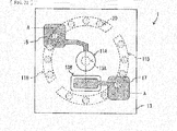
- FIG. 13 illustrates an example in which the light-emitting device 1 is mounted on a wiring substrate 30.
- the wiring substrate 30 includes a plurality of electrode pads 31 on a surface.
- An in-plane layout of the plurality of electrode pads 31 is common to an in-plane layout of the plurality of convex portions 11B (or the convex portions 10B), for example.
- the light-emitting device 1 is mounted on the wiring substrate 30 with the plurality of the convex portions 10B directed to the wiring substrate 30 side.
- the plurality of the convex portions 10B is fixed to the plurality of electrode pads 31 via a solder bump 32.
- each of the convex portions 10B has a height greater than or equal to the height of the convex portion 10A, thus allowing each of the convex portions 11B to play a role to protect the convex portion 11A, for example, in the process of mounting the light-emitting device 1 on the wiring substrate 30.
- the laminate 12 includes a nitride-based semiconductor material
- blue laser light is emitted from the DBR layer 16.
- the metal layer 19 it is possible to cause the metal layer 19 to have a function similar to the function of the electrode pad 17 by electrically coupling the metal layer 19 to the semiconductor layer 12a via the substrate 11 exposed into the opening of the DBR layer 18.
- a reflecting mirror of a surface-emitting laser is shaped into a concave curve
- an opening is formed by etching of a portion of a substrate immediately under a light-emitting device, and lens processing is performed on a bottom surface of the opening.
- the method of PTL1 has a high level of technical difficulty and is not suitable for mass production. Moreover, etching damage remains on a bottom surface of the opening, and thus, the bottom surface of the opening is not suitable for lens formation. Furthermore, it is not known whether or not it is possible to use a spot of the substrate corresponding to an edge of the opening for positioning when a light-emitting device is mounted.
- the convex portion 11A having a convex-curved shape, in contact with the DBR layer 18, and faces the opening 13A.
- the plurality of the convex portions 11B each having a height greater than or equal to the height of the convex portion 11A is further provided around the convex portion 11A.
- the surface of the end on the convex portion 11A side has a convex-curved shape.
- the mounting position of the light-emitting device 1 is determined by the self-alignment function of the convex curve of the metal layer 19 (convex portion 10B) formed following the convex curve of the convex portion 11B.
- the convex portion 11A is protected by the convex portion 11B in a manufacturing process or a mounting process of the light-emitting device 1. Consequently, it is possible to precisely align the light-emitting device 1 with the wiring substrate 30 and to protect the DBR layer 18.
- the convex portion 11A and each of the convex portions 10B are island-shaped. Consequently, performing the resist etch-back utilizing the relation, for example, illustrated in FIG. 3 allows each of the convex portions 11B to be higher than or equal to the convex portion 11A and also makes it possible to collectively form the convex portion 11A and the respective convex portions 11B. Consequently, it is possible to precisely align the light-emitting device 1 with the wiring substrate 30 without requesting an additional manufacturing procedure and to protect the DBR layer 18. Moreover, simultaneous formation of the convex portion 11 and the respective convex portions 10B is possible, and it is thus possible to avoid aggravated roughness due to damage from unnecessary etching. This makes it possible to suppress diffraction loss due to aggravated roughness and also to suppress a crack, etc. due to stress concentration.
- the substrate 11 is a GaN substrate. Consequently, performing the resist etch-back utilizing the relation, for example, illustrated in FIG. 3 on the GaN substrate allows each of the convex portions 11B to be higher than or equal to the convex portion 11A and also makes it possible to collectively form the convex portion 11A and the respective convex portions 11B. Consequently, it is possible to precisely align the light-emitting device 1 with the wiring substrate 30 without requesting an additional manufacturing procedure and to protect the DBR layer 18. Moreover, simultaneous formation of the convex portion 11 and the respective convex portions 10B is possible, and it is thus possible to avoid aggravated roughness due to damage from unnecessary etching. This makes it possible to suppress diffraction loss due to aggravated roughness and also to suppress a crack, etc. due to stress concentration.
- the reflow is performed on the island-shaped resist layer 23A and the plurality of island-shaped resist layers 23B provided on the rear surface of the substrate 11 in the manufacturing process.
- This shapes the surface of the resist layer 23A into a convex curve, and shapes at least each of the ends of the surfaces of the plurality of resist layers 23B on the resist layer 23A side into a convex curve.
- the dry etching using the resist etch-back method is performed with the resist layer 23A and the plurality of resist layers 23B subjected to the reflow as the mask.
- the convex portion 11A having a convex-curved shape is formed at the spot where the resist layer 23A has been formed, and the plurality of convex portions 11B at least ends of which on the resist layer 23A side each have a convex-curved shape is formed at the spot where the plurality of resist layers 23B has been formed.
- the width R1 and the width R2 of the resist layer 23A and each of the plurality of resist layers 23B are set by the reflow and the resist etch-back to cause each of the convex portions 11B to have a height greater than or equal to the height of the convex portion 11A.
- the mounting position of the light-emitting device 1 is determined by the self-alignment function of the convex curve of the metal layer 19 formed following the convex curve of the convex portion 11B.
- the convex portion 11A is protected by the convex portion 11B in a manufacturing process or a mounting process of the light-emitting device 1. Accordingly, it is possible to precisely align the light-emitting device 1 with the wiring substrate 30 without requesting an additional manufacturing procedure and to protect the DBR layer 18.
- simultaneous formation of the convex portion 11 and the respective convex portions 10B is possible, and it is thus possible to avoid aggravated roughness due to damage from unnecessary etching. This makes it possible to suppress diffraction loss due to aggravated roughness and also to suppress a crack, etc. due to stress concentration.
- the one resist layer 23A is formed and the two or more resist layers 23B are formed. Furthermore, the resist layer 23A and the respective resist layers 23B are formed in the island shape. With this, simply setting the width R1 and the width R2 of the resist layer 23A and the plurality of resist layers 23B to a predetermined value makes it possible to make the height of each of the convex portions 11B greater than or equal to the height of the convex portion 11A. Accordingly, it is possible to precisely align the light-emitting device 1 with the wiring substrate 30 without requesting an additional manufacturing procedure and to protect the DBR layer 18.
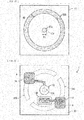
- FIG. 14 illustrates a modification example of the light-emitting device 1.
- the convex portion 11B has an annular shape.
- the convex portion 11B has, for example, a toric shape, an elliptical ring shape, or a polygonal ring shape.
- the convex portion1 11A is disposed in the opening of the convex portion 11B.
- the convex portions 11B are provided avoiding the position facing the opening 13A.
- the convex portions 11B are provided around the convex portion 11A.
- the convex portions 11B are disposed at point-symmetric positions about the convex portion 11A, for example.
- the convex portion 11B has the height greater than or equal to the height of the convex portion 11A, and at least a surface of an end (end on the inner perimeter side) on the convex portion 11A side has a convex-curved shape.
- a whole surface of the convex portion 11B may have a convex-curved shape, protruding to the side opposite to the laminate 12 in the width direction of the convex portion 11B.
- the height of the convex portion 11B is formed by etching of the substrate 11 with the reflowed annular resist layer as the mask, as described later.
- the width of the reflowed annular resist layer corresponds to the lens diameter of FIG. 3 . That is, changing the width of the reflowed annular resist layer may make it possible to adjust the height or the radius of curvature of the convex portion 11B in the width direction.
- a design is assumed that makes the width of the annular resist layer to be used in formation of the convex portion 11B smaller than the diameter of the island-shaped resist layer to be used in formation of the convex portion 11A.
- the diameter of the island-shaped resist layer to be used in the formation of the convex portion 11A is 80 ⁇ m
- the width of the annular resist layer to be used in the formation of the convex portion 11B is greater than or equal to 30 ⁇ m and less than or equal to 70 ⁇ m.
- the diameter of the convex portion 11A is 80 ⁇ m
- the width of the convex portion 11B is greater than or equal to 30 ⁇ m and less than or equal to 70 ⁇ m
- the radius of curvature of the surface of the convex portion 11B is smaller than the radius of curvature of the convex portion 11A.
- the width of the annular resist layer to be used in formation of the convex portion 11B is larger than the diameter of the island-shaped resist layer to be used in formation of the convex portion 11A.
- the diameter of the island-shaped resist layer to be used in the formation of the convex portion 11A is 30 ⁇ m
- the width of the annular resist layer to be used in the formation of the convex portion 11B is greater than or equal to 40 ⁇ m and less than or equal to 60 ⁇ m.
- the diameter of the convex portion 11A is 30 ⁇ m
- the width of the convex portion 11B is greater than or equal to 40 ⁇ m and less than or equal to 60 ⁇ m
- the radius of curvature of the surface of the convex portion 11B is larger than the radius of curvature of the convex portion 11A.
- the convex portions 11A and 11B are formed, for example, as described below.
- the rear surface of the substrate 11 is mirror-finished.
- a resist pattern is formed on the polished rear surface of the substrate 11.
- a resist layer 23A first resist layer
- the resist layers 23B second resist layers
- the width R1 and the width R2 of the resist layer 23A and the resist layer 23B are set by the reflow and the resist etch-back to cause each of the convex portions 11B to have a height greater than or equal to the height of the convex portion 11A.
- the width R1 and the width R2 of the resist layer 23A and the resist layer 23B are set on the basis of the relation described in FIG. 3 to cause the height of the convex portion 11B to be greater than or equal to the height of the convex portion 11A.
- a design is assumed that makes the width of the annular resist layer 23B to be used in formation of the convex portion 11B smaller than the diameter of the island-shaped resist layer 23A to be used in formation of the convex portion 11A.
- the width R1 of the resist layer 23A is 80 ⁇ m
- the width R2 of the resist layer 23B is greater than or equal to 30 ⁇ m and less than or equal to 70 ⁇ m.
- the diameter of the convex portion 11A is 80 ⁇ m
- the width of the convex portion 11B is greater than or equal to 30 ⁇ m and less than or equal to 70 ⁇ m
- the radius of curvature of the surface of the convex portion 11B is smaller than the radius of curvature of the convex portion 11A.
- the width of the annular resist layer 23B to be used in formation of the convex portion 11B larger than the diameter of the island-shaped resist layer 23A to be used in formation of the convex portion 11A.
- the width R1 of the resist layer 23A is 30 ⁇ m
- the width R2 of the resist layer 23B is greater than or equal to 40 ⁇ m and less than or equal to 60 ⁇ m.
- the diameter of the convex portion 11A is 30 ⁇ m
- the width of the convex portion 11B is greater than or equal to 40 ⁇ m and less than or equal to 60 ⁇ m
- the radius of curvature of the surface of the convex portion 11B is larger than the radius of curvature of the convex portion 11A.
- the reflow is performed on the resist layers 23A and 23B.
- the whole surface of the resist layer 23A is shaped into a convex curve, and the surface of the resist layer 23B in the width direction is shaped into a convex curve.
- the height of the resist layer 23B is greater than or equal to the height of the resist layer 23A.
- dry etching is performed on the substrate 11 with the resist layers 23A and 23B, the surfaces of which each have a convex-curved shape, as a mask. That is, the dry etching using the resist etch-back method is performed on the substrate 11 with the resist layers 23A and 23B subjected to the reflow as the mask. At this time, it is preferable that the etching speed of the substrate 11 and the etching speed of the resist layers 23A and 23B be as equal as possible.
- the use of such a resist etch-back method makes it possible to form, on the rear surface of the substrate 11, the convex portions 11A and 11B each having a convex-curved shape similar to a surface shape of the resist layers 23A and 23B.
- the convex portion 11A having a convex-curved shape at the spot where the resist layer 23A has been formed and to form, and form, at the spot where each of the resist layers 23B has been formed, the convex portion 11B at least an end (end on the inner perimeter side) of which on the convex portion 11A side has a surface having a convex-curved shape.
- the height of each of the convex portions 11B is greater than or equal to the height of the convex portion 11A.
- the convex portion 11A having a convex-curved shape, in contact with the DBR layer 18, and faces the opening 13A.
- the annular convex portions 11B each having a height greater than or equal to the height of the convex portion 11A are further provided around the convex portion 11A.
- the annular convex portions 11B at least the surface of the end (end on the inner perimeter side) on the convex portion 11A side has a convex-curved shape.
- the mounting position of the light-emitting device 1 is determined by the self-alignment function of the convex curve of the metal layer 19 (convex portion 10B) formed following the convex curve of the convex portion 11B.
- the convex portion 11A is protected by the convex portion 11B in a manufacturing process or a mounting process of the light-emitting device 1. Consequently, it is possible to precisely align the light-emitting device 1 with the wiring substrate 30 and to protect the DBR layer 18.
- the convex portion 11A is island-shaped, and the convex portion 10B has an annular shape. Consequently, performing the resist etch-back utilizing the relation, for example, illustrated in FIG. 3 allows each of the convex portions 11B to be higher than or equal to the convex portion 11A and also makes it possible to collectively form the convex portion 11A and the respective convex portions 11B. Consequently, it is possible to precisely align the light-emitting device 1 with the wiring substrate 30 without requesting an additional manufacturing procedure and to protect the DBR layer 18. Moreover, simultaneous formation of the convex portion 11 and the convex portions 10B is possible, and it is thus possible to avoid aggravated roughness due to damage from unnecessary etching. This makes it possible to suppress diffraction loss due to aggravated roughness and also to suppress a crack, etc. due to stress concentration.
- the reflow is performed on the island-shaped resist layer 23A and the annular resist layers 23B provided on the rear surface of the substrate 11 in the manufacturing process.
- This shapes the surface of the resist layer 23A into a convex curve, and shapes at least each of the surfaces of the ends (ends on the inner perimeter side) of the surfaces of the resist layers 23B on the resist layer 23A side into a convex curve.
- the dry etching using the resist etch-back method is performed with the resist layer 23A and the resist layers 23B subjected to the reflow as the mask.
- the convex portion 11A having a convex-curved shape is formed at the spot where the resist layer 23A has been formed, and the convex portions 11B at least ends (ends on the inner perimeter side) of which on the resist layer 23A side each have a surface having a convex-curved shape are formed at the spot where the resist layers 23B have been formed.
- the width R1 and the width R2 of the resist layer 23A and each of the resist layers 23B are set by the reflow and the resist etch-back to cause each of the convex portions 11B to have a height greater than or equal to the height of the convex portion 11A.
- the mounting position of the light-emitting device 1 is determined by the self-alignment function of the convex curve of the metal layer 19 formed following the convex curve of the convex portion 11B.
- the convex portion 11A is protected by the convex portion 11B in a manufacturing process or a mounting process of the light-emitting device 1. Accordingly, it is possible to precisely align the light-emitting device 1 with the wiring substrate 30 without requesting an additional manufacturing procedure and to protect the DBR layer 18.
- simultaneous formation of the convex portion 11 and the convex portions 10B is possible, and it is thus possible to avoid aggravated roughness due to damage from unnecessary etching. This makes it possible to suppress diffraction loss due to aggravated roughness and also to suppress a crack, etc. due to stress concentration.
- the one resist layer 23A is formed and the one resist layer 23B is formed. Furthermore, the resist layer 23A is formed in the island shape and the resist layer 23B is formed in the annular shape.
- simply setting the width R1 and the width R2 of the resist layer 23A and each of the resist layers 23B to a predetermined value makes it possible to make the height of each of the convex portions 11B greater than or equal to the height of the convex portion 11A. Accordingly, it is possible to precisely align the light-emitting device 1 with the wiring substrate 30 without requesting an additional manufacturing procedure and to protect the DBR layer 18.
- FIG. 16 illustrates a modification example of the light-emitting device 1.
- the two or more convex portions 11B are provided.
- the plurality of the convex portions 11B has a shape and a layout in which the annular convex portion is divided into a plurality of portions.
- Each of the convex portions 11B has the shape of a straight bar or the shape of a curved bar.
- the plurality of convex portions 11B is provided avoiding the position facing the opening 13A.
- the plurality of convex portions 11B is provided around the convex portion 11A.
- the plurality of convex portions 11B is disposed at point-symmetric positions about the convex portion 11A, for example.
- Each convex portion 11B has the height greater than or equal to the height of the convex portion 11A, and at least a surface of an end on the convex portion 11A side has a convex-curved shape.
- a whole surface of each convex portion 11B may have a convex-curved shape, protruding to the side opposite to the laminate 12 in the width direction of the convex portion 11B.
- the height of the convex portion 11B is formed by etching of the substrate 11 with the reflowed bar-shaped resist layer as the mask, as described later.
- the width of the reflowed bar-shaped resist layer corresponds to the lens diameter of FIG. 3 . That is, changing the width of the reflowed bar-shaped resist layer may make it possible to adjust the height or the radius of curvature of the convex portion 11B in the width direction.
- a design is assumed that makes the width of the bar-shaped resist layer to be used in formation of the convex portion 11B smaller than the diameter of the island-shaped resist layer to be used in formation of the convex portion 11A.
- the diameter of the island-shaped resist layer to be used in the formation of the convex portion 11A is 80 ⁇ m
- the width of the bar-shaped resist layer to be used in the formation of the convex portion 11B is greater than or equal to 30 ⁇ m and less than or equal to 70 ⁇ m.
- the diameter of the convex portion 11A is 80 ⁇ m
- the width of the convex portion 11B is greater than or equal to 30 ⁇ m and less than or equal to 70 ⁇ m
- the radius of curvature of the surface of the convex portion 11B is smaller than the radius of curvature of the convex portion 11A.
- the width of the bar-shaped resist layer to be used in formation of the convex portion 11B larger than the diameter of the island-shaped resist layer to be used in formation of the convex portion 11A.
- the diameter of the island-shaped resist layer to be used in the formation of the convex portion 11A is 30 ⁇ m
- the width of the bar-shaped resist layer to be used in the formation of the convex portion 11B is greater than or equal to 40 ⁇ m and less than or equal to 60 ⁇ m.
- the diameter of the convex portion 11A is 30 ⁇ m
- the width of the convex portion 11B is greater than or equal to 40 ⁇ m and less than or equal to 60 ⁇ m
- the radius of curvature of the surface of the convex portion 11B is larger than the radius of curvature of the convex portion 11A.
- the convex portions 11A and 11B are formed, for example, as described below.
- the rear surface of the substrate 11 is mirror-finished.
- a resist pattern is formed on the polished rear surface of the substrate 11.
- the resist layer 23A first resist layer
- each of the resist layers 23B second resist layers
- the width R1 and the width R2 of the resist layer 23A and the resist layer 23B are set by the reflow and the resist etch-back to cause each of the convex portions 11B to have a height greater than or equal to the height of the convex portion 11A.
- the width R1 and the width R2 of the resist layer 23A and the resist layer 23B are set on the basis of the relation described in FIG. 3 to cause the height of the convex portion 11B to be greater than or equal to the height of the convex portion 11A.
- a design is assumed that makes the width of the bar-shaped resist layer 23B to be used in formation of the convex portion 11B smaller than the diameter of the island-shaped resist layer 23A to be used in formation of the convex portion 11A.
- the width R1 of the resist layer 23A is 80 ⁇ m
- the width R2 of the resist layer 23B is greater than or equal to 30 ⁇ m and less than or equal to 70 ⁇ m.
- the diameter of the convex portion 11A is 80 ⁇ m
- the width of the convex portion 11B is greater than or equal to 30 ⁇ m and less than or equal to 70 ⁇ m
- the radius of curvature of the surface of the convex portion 11B is smaller than the radius of curvature of the convex portion 11A.
- the width of the bar-shaped resist layer 23B to be used in formation of the convex portion 11B larger than the diameter of the island-shaped resist layer 23A to be used in formation of the convex portion 11A.
- the width R1 of the resist layer 23A is 30 ⁇ m
- the width R2 of the resist layer 23B is greater than or equal to 40 ⁇ m and less than or equal to 60 ⁇ m.
- the diameter of the convex portion 11A is 30 ⁇ m
- the width of the convex portion 11B is greater than or equal to 40 ⁇ m and less than or equal to 60 ⁇ m
- the radius of curvature of the surface of the convex portion 11B is larger than the radius of curvature of the convex portion 11A.
- the reflow is performed on the resist layers 23A and 23B.
- the whole surface of the resist layer 23A is shaped into a convex curve, and the surface of the resist layer 23B in the width direction is shaped into a convex curve.
- the height of the resist layer 23B is greater than or equal to the height of the resist layer 23A.
- dry etching is performed on the substrate 11 with the resist layers 23A and 23B, the surfaces of which each have a convex-curved shape, as a mask. That is, the dry etching using the resist etch-back method is performed on the substrate 11 with the resist layers 23A and 23B subjected to the reflow as the mask. At this time, it is preferable that the etching speed of the substrate 11 and the etching speed of the resist layers 23A and 23B be as equal as possible.
- the use of such a resist etch-back method makes it possible to form, on the rear surface of the substrate 11, the convex portions 11A and 11B each having a convex-curved shape similar to a surface shape of the resist layers 23A and 23B.
- the convex portion 11A having a convex-curved shape at the spot where the resist layer 23A has been formed and to form, and form, at the spot where each of the resist layers 23B has been formed, the convex portion 11B at least an end (end on the inner perimeter side) of which on the convex portion 11A side has a surface having a convex-curved shape.
- the height of each of the convex portions 11B is greater than or equal to the height of the convex portion 11A.
- the convex portion 11A having a convex-curved shape, in contact with the DBR layer 18, and faces the opening 13A.
- the plurality of bar-shaped convex portions 11B each having a height greater than or equal to the height of the convex portion 11A is further provided around the convex portion 11A.
- at least the surface of the end on the convex portion 11A side has a convex-curved shape.
- the mounting position of the light-emitting device 1 is determined by the self-alignment function of the convex curve of the metal layer 19 (convex portion 10B) formed following the convex curve of the convex portion 11B.
- the convex portion 11A is protected by the convex portion 11B in a manufacturing process or a mounting process of the light-emitting device 1. Consequently, it is possible to precisely align the light-emitting device 1 with the wiring substrate 30 and to protect the DBR layer 18.
- the convex portion 11A is island-shaped, and the convex portion 10B is bar-shaped. Consequently, performing the resist etch-back utilizing the relation, for example, illustrated in FIG. 3 allows each of the convex portions 11B to be higher than or equal to the convex portion 11A and also makes it possible to collectively form the convex portion 11A and the respective convex portions 11B.
- a gap is present between the two convex portions 10B adjacent to each other, thus making it possible to control a position into which a polishing solution is poured by using the gap thereof, when the convex portion 11A, for example, is polished by CMP, etc.
- the reflow is performed on the island-shaped resist layer 23A and the bar-shaped resist layers 23B provided on the rear surface of the substrate 11 in the manufacturing process.
- This shapes the surface of the resist layer 23A into a convex curve, and shapes at least each of the surfaces of the ends of the surfaces of the resist layers 23B on the resist layer 23A side into a convex curve.
- the dry etching using the resist etch-back method is performed with the resist layer 23A and the resist layers 23B subjected to the reflow as the mask.
- the convex portion 11A having a convex-curved shape is formed at the spot where the resist layer 23A has been formed, and the convex portions 11B at least ends of which on the resist layer 23A side each have a surface having a convex-curved shape are formed at the spot where the resist layers 23B have been formed.
- the width R1 and the width R2 of the resist layer 23A and each of the resist layers 23B are set by the reflow and the resist etch-back to cause each of the convex portions 11B to have a height greater than or equal to the height of the convex portion 11A.
- the mounting position of the light-emitting device 1 is determined by the self-alignment function of the convex curve of the metal layer 19 formed following the convex curve of the convex portion 11B.
- the convex portion 11A is protected by the convex portion 11B in a manufacturing process or a mounting process of the light-emitting device 1. Accordingly, it is possible to precisely align the light-emitting device 1 with the wiring substrate 30 without requesting an additional manufacturing procedure and to protect the DBR layer 18.
- simultaneous formation of the convex portion 11 and the convex portions 10B is possible, and it is thus possible to avoid aggravated roughness due to damage from unnecessary etching. This makes it possible to suppress diffraction loss due to aggravated roughness and also to suppress a crack, etc. due to stress concentration.
- the one resist layer 23A is formed and the two or more resist layers 23B are formed. Furthermore, the resist layer 23A is formed in the island shape and the resist layers 23B are formed in the bar shape. With this, simply setting the width R1 and the width R2 of the resist layer 23A and each of the resist layers 23B to a predetermined value makes it possible to make the height of each of the convex portions 11B greater than or equal to the height of the convex portion 11A. Accordingly, it is possible to precisely align the light-emitting device 1 with the wiring substrate 30 without requesting an additional manufacturing procedure and to protect the DBR layer 18.
- FIG. 18 illustrates a modification example of the light-emitting device 1 of FIG. 1 .
- FIG. 19 illustrates a top configuration example of the light-emitting device 1 of FIG. 18 .
- FIG. 20 illustrates a modification example of the light-emitting device 1 of FIG. 2 .
- FIG. 21 illustrates a modification example of the light-emitting device 1 of FIG. 2 .
- the light-emitting device 1 according to the modification example corresponds to the light-emitting device 1 according to the aforementioned embodiment in which a bump 20 (bump metal) is further provided at a position facing the convex portions 11B and 11C.
- the bump 20 is provided in a through-hole that penetrates through the DBR layer 18 and the metal layer 19, for example.
- the bump 20 has a height greater than or equal to the height of the convex portion 10A.
- the height of the bump 20 refers to a height from the flat surface 11S corresponding to a base of the convex portion 11A on the rear surface of the substrate 11. Even in such a configuration, the bump 20 attains the function similar to the functions of the convex portions 10B and 10C according to the aforementioned embodiment. Consequently, it is possible to precisely align the light-emitting device 1 with the wiring substrate 30 and to protect the DBR layer 18.
Claims (11)
- Lichtemittierende Vorrichtung (1), umfassend:ein Laminat (12), das eine aktive Schicht (12b) sowie eine erste Halbleiterschicht (12a) und eine zweite Halbleiterschicht (12c) einschließt, welche die aktive Schicht sandwich-artig umgeben;eine Strombegrenzungsschicht (13) mit einer Öffnung (13A);einen ersten reflektierenden Spiegel (18) auf der ersten Halbleiterschichtseite und einen zweiten reflektierenden Spiegel (16) auf der zweiten Halbleiterschichtseite, wobei der erste reflektierende Spiegel und der zweite reflektierende Spiegeln das Laminat und die Öffnung sandwich-artig umgeben, wobei der erste reflektierende Spiegel eine konkav gekrümmte Form aufweist; undein optisch transparentes Substrat (11), das zwischen dem ersten reflektierenden Spiegel und dem Laminat bereitgestellt wird,wobei das optisch transparente Substrat auf einer Oberfläche auf einer Seite, die dem Laminat gegenüber liegt, einschließt:einen ersten konvexen Anteil (11A) in Kontakt mit dem ersten reflektierenden Spiegel, wobei der erste konvexe Anteil eine konvex gekrümmte Form aufweist, die auf der Seite vorspringt, die dem Laminat gegenüber liegt, undeinen oder mehrere zweite konvexe Anteile, der/die um den ersten konvexen Anteil bereitgestellt wird/werden, wobei der eine oder die mehreren zweiten konvexen Anteile (11B) jeweils eine Höhe größer als oder gleich einer Höhe des ersten konvexen Anteils aufweisen, wobei die Höhe jedes konvexen Anteils eine Höhe ab einer flachen Oberfläche (11S) ist, die einer Basis des jeweiligen konvexen Anteils auf einer rückwärtigen Oberfläche des Substrats entspricht, und wobei jeder ein Ende auf der ersten konvexen Anteilseite aufweist, das zu einer konvexen Krümmung geformt ist; des Weiteren umfassend Höckermetall (20), das in einer Position gebildet ist, die zu dem zweiten konvexen Anteil weist.
- Licht emittierende Vorrichtung nach Anspruch 1, wobei der erste reflektierende Spiegel einer Oberfläche folgend gebildet wird, die eine Oberfläche des ersten konvexen Anteils und eine Oberfläche des zweiten konvexen Anteils einschließt.
- Licht emittierende Vorrichtung nach Anspruch 2, des Weiteren umfassend eine Metallschicht, die einer Oberfläche des ersten reflektierenden Spiegels folgend gebildet ist.
- Licht emittierende Vorrichtung nach Anspruch 1, wobei
das optisch transparente Substrat eine Vielzahl der zweiten konvexen Anteile einschließt, und jeder der zweiten konvexen Anteile inselförmig ist. - Licht emittierende Vorrichtung nach Anspruch 1, wobeidas optisch transparente Substrat den einen zweiten konvexen Anteil einschließt, undder zweite konvexe Anteil eine torische Form aufweist.
- Licht emittierende Vorrichtung nach Anspruch 1, wobeidas optisch transparente Substrat eine Vielzahl der zweiten konvexen Anteile einschließt, undeine Vielzahl der zweiten konvexen Anteile eine Form und ein Layout aufweist, bei dem ein kranzförmiger konvexer Anteil in eine Vielzahl von Anteilen geteilt wird.
- Licht emittierende Vorrichtung nach Anspruch 1, wobei das optisch transparente Substrat ein GaN-Substrat ist.
- Verfahren zum Fertigen einer Licht emittierenden Vorrichtung (1), wobei das Verfahren umfasst:einen Resistbildungsschritt (S102) des Bildens in einem Substrat einer Licht emittierenden Vorrichtung, welches auf einer ersten Hauptoberfläche eines optisch transparenten Substrats (11) ein Laminat (12), das eine aktive Schicht (12b) sowie eine erste Halbleiterschicht (12a) und eine zweite Halbleiterschicht einschließt, welche die aktive Schicht sandwich-artig umgeben, und eine Strombegrenzungsschicht (13) mit einer Öffnung (13A) einschließt, einer ersten Resistschicht an einem Punkt, der zu der Öffnung weist, und des Bildens von einer oder mehreren zweiten Resistschichten um den Punkt herum, der zu der Öffnung weist, auf einer zweiten Hauptoberfläche des optisch transparenten Substrats auf einer Seite, welche der ersten Hauptoberfläche gegenüber liegt;einen Reflow (S103)-Schritt des Durchführens von Reflow (Wiederaufschmelzen) an der ersten Resistschicht und der einen oder zweiten Resistschichten, wodurch eine Oberfläche der ersten Resistschicht zu einer konvexen Krümmung geformt wird und mindestens jedes der Enden der Oberflächen der einen oder mehreren zweiten Resistschichten auf der ersten Resistschichtseite zu einer konvexen Krümmung geformt wird; undeinen Bildungsschritt des konvexen Anteils (S104, S105) des Bildens eines ersten konvexen Anteils (11A) mit einer konvex gekrümmten Form, die an der Seite vorspringt, die dem Laminat gegenüber liegt, an einem Punkt, an dem die erste Resistschicht gebildet worden ist, auf der zweiten Hauptoberfläche des Substrats, und Bilden eines zweiten konvexen Anteils (11B), wobei mindestens ein Ende davon auf der ersten Resistschichtseite eine konvex gekrümmte Form an einem Punkt aufweist, an dem die eine oder mehreren zweiten Resistschichten gebildet worden sind, indem unter Verwendung eines Resist-Rückätzverfahrens Trockenätzung mit der ersten Resistschicht und der einen oder den mehreren zweiten Resistschichten, welche dem Reflow ausgesetzt sind, als Maske durchgeführt wird,wobei eine Breite von jeder der ersten Resistschicht und der einen oder den mehreren zweiten Resistschichten in dem Resistbildungsschritt durch den Reflow und das Resist-Rückätzen festgelegt wird, um zu bewirken, dass jeder der zweiten konvexen Anteile eine Höhe größer als oder gleich einer Höhe des ersten konvexen Anteils aufweist, wobei die Höhe jedes konvexen Anteils eine Höhe ab einer flachen Oberfläche (11S) ist, die einer Basis des jeweiligen konvexen Anteils auf einer rückwärtigen Oberfläche des Substrats entspricht; des Weiteren umfassend einen Höckermetallbildungsschritt des Bildens von Höckermetall (20) an einer Position, die zu dem zweiten konvexen Anteil weist.
- Verfahren zur Fertigung der Licht emittierenden Vorrichtung nach Anspruch 8, wobei in dem Resistbildungsschritt die eine erste Resistschicht gebildet wird, die zwei oder mehr zweiten Resistschichten gebildet werden, und die erste Resistschicht und jede der zweiten Resistschichten des Weiteren zu einer Inselform gebildet werden.
- Verfahren zur Fertigung der Licht emittierenden Vorrichtung nach Anspruch 8, wobei in dem Resistbildungsschritt die eine erste Resistschicht gebildet wird, die eine zweite Resistschicht gebildet wird, die erste Resistschicht des Weiteren zu einer Inselform gebildet wird, und die zweite Resistschicht zu einer torischen Form gebildet wird.
- Verfahren zur Fertigung der Licht emittierenden Vorrichtung nach Anspruch 8, wobei in dem Resistbildungsschritt die eine erste Resistschicht gebildet wird, die zwei oder mehr zweiten Resistschichten gebildet werden, die erste Resistschicht des Weiteren zu einer Inselform gebildet wird, und jede der zweiten Resistschichten so gebildet wird, dass sie eine Form und ein Layout aufweist, so dass ein kranzförmiger konvexer Anteil in eine Vielzahl von Anteilen geteilt wird.
Applications Claiming Priority (2)
| Application Number | Priority Date | Filing Date | Title |
|---|---|---|---|
| JP2017107830 | 2017-05-31 | ||
| PCT/JP2018/015716 WO2018221042A1 (ja) | 2017-05-31 | 2018-04-16 | 発光素子および発光素子の製造方法 |
Publications (3)
| Publication Number | Publication Date |
|---|---|
| EP3633807A1 EP3633807A1 (de) | 2020-04-08 |
| EP3633807A4 EP3633807A4 (de) | 2020-06-17 |
| EP3633807B1 true EP3633807B1 (de) | 2021-12-29 |
Family
ID=64455062
Family Applications (1)
| Application Number | Title | Priority Date | Filing Date |
|---|---|---|---|
| EP18810741.1A Active EP3633807B1 (de) | 2017-05-31 | 2018-04-16 | Lichtemittierendes element und herstellungsverfahren für lichtemittierendes element |
Country Status (4)
| Country | Link |
|---|---|
| US (1) | US11374384B2 (de) |
| EP (1) | EP3633807B1 (de) |
| JP (1) | JPWO2018221042A1 (de) |
| WO (1) | WO2018221042A1 (de) |
Families Citing this family (6)
| Publication number | Priority date | Publication date | Assignee | Title |
|---|---|---|---|---|
| EP3890128A1 (de) * | 2017-06-28 | 2021-10-06 | Sony Group Corporation | Lichtemittierendes element und herstellungsverfahren |
| KR102544296B1 (ko) * | 2018-09-13 | 2023-06-16 | 쑤저우 레킨 세미컨덕터 컴퍼니 리미티드 | 표면발광레이저 소자 및 이를 구비한 표면발광레이저 장치 |
| US20230057446A1 (en) * | 2020-01-08 | 2023-02-23 | Sony Group Corporation | Light emitting element |
| EP4175080A4 (de) * | 2020-06-25 | 2024-01-03 | Sony Group Corp | Lichtemittierende vorrichtung |
| JPWO2022176434A1 (de) * | 2021-02-22 | 2022-08-25 | ||
| WO2023145271A1 (ja) * | 2022-01-27 | 2023-08-03 | ソニーグループ株式会社 | 面発光素子、光源装置及び面発光素子の製造方法 |
Family Cites Families (51)
| Publication number | Priority date | Publication date | Assignee | Title |
|---|---|---|---|---|
| US4935939A (en) * | 1989-05-24 | 1990-06-19 | Liau Zong Long | Surface emitting laser with monolithic integrated lens |
| JPH03263023A (ja) | 1990-03-14 | 1991-11-22 | Minolta Camera Co Ltd | リーダプリンタ |
| JPH0555703A (ja) * | 1991-05-15 | 1993-03-05 | Fujitsu Ltd | 面発光レーザ装置 |
| JPH0575207A (ja) * | 1991-09-13 | 1993-03-26 | Nippon Telegr & Teleph Corp <Ntt> | 共振器型半導体光装置及びその製法 |
| JP3244529B2 (ja) * | 1992-04-16 | 2002-01-07 | アジレント・テクノロジーズ・インク | 面発光型第2高調波生成素子 |
| US5796714A (en) * | 1994-09-28 | 1998-08-18 | Matsushita Electric Industrial Co., Ltd. | Optical module having a vertical-cavity surface-emitting laser |
| JPH0911791A (ja) | 1995-06-27 | 1997-01-14 | Nippon Yusoki Co Ltd | ヘッドランプ・ロービーム点消灯装置 |
| JPH10200200A (ja) | 1997-01-06 | 1998-07-31 | Canon Inc | 面発光型半導体レーザ |
| JPH10335383A (ja) * | 1997-05-28 | 1998-12-18 | Matsushita Electric Ind Co Ltd | 半導体装置の製造方法 |
| KR100273134B1 (ko) * | 1997-11-29 | 2001-01-15 | 정선종 | 단일모드표면방출레이저및그제조방법 |
| JP3362836B2 (ja) | 1997-12-26 | 2003-01-07 | 日亜化学工業株式会社 | 光半導体素子の製造方法 |
| JP3559453B2 (ja) * | 1998-06-29 | 2004-09-02 | 株式会社東芝 | 発光素子 |
| US6657233B2 (en) * | 1998-08-19 | 2003-12-02 | Ricoh Company, Ltd. | Light emitting devices with layered III-V semiconductor structures, and modules and systems for computer, network and optical communication, using such device |
| KR100393057B1 (ko) * | 2000-10-20 | 2003-07-31 | 삼성전자주식회사 | 마이크로 렌즈 일체형 표면광 레이저 |
| KR100374796B1 (ko) * | 2001-02-02 | 2003-03-03 | 삼성전기주식회사 | P형 전극과 활성층 사이에 효과적인 정공 확산을 위한 스페이서를 구비하는 GaN 면 발광 레이저 다이오드 및그 제조 방법 |
| EP1265327B1 (de) * | 2001-06-02 | 2007-11-07 | Seoul National University Industry Foundation | Oberflächenemittierender Laser mit vertikalem Resonator |
| JP2003017806A (ja) * | 2001-06-29 | 2003-01-17 | Toshiba Corp | 化合物半導体発光素子とその製造方法および化合物半導体発光装置 |
| JP4131623B2 (ja) | 2001-09-12 | 2008-08-13 | 三洋電機株式会社 | 電極構造およびその製造方法 |
| US6853007B2 (en) * | 2001-12-28 | 2005-02-08 | Finisar Corporation | Submount for vertical cavity surface emitting lasers and detectors |
| WO2005067113A1 (ja) * | 2004-01-07 | 2005-07-21 | Hamamatsu Photonics K.K. | 半導体発光素子及びその製造方法 |
| JP4116587B2 (ja) * | 2004-04-13 | 2008-07-09 | 浜松ホトニクス株式会社 | 半導体発光素子及びその製造方法 |
| JP2007114454A (ja) * | 2005-10-20 | 2007-05-10 | Yamaha Corp | マイクロレンズアレイとその製法 |
| JP2008244240A (ja) * | 2007-03-28 | 2008-10-09 | Seiko Epson Corp | 面発光型半導体レーザおよびその製造方法、ならびに光モジュール |
| GB2448161A (en) * | 2007-04-03 | 2008-10-08 | Bookham Technology Plc | Optoelectronic device combining VCSEL and photodetector |
| JP5250245B2 (ja) * | 2007-11-21 | 2013-07-31 | 日本オクラロ株式会社 | 半導体レーザ |
| JP5221180B2 (ja) * | 2008-03-28 | 2013-06-26 | Dowaエレクトロニクス株式会社 | 発光素子 |
| JP5342838B2 (ja) * | 2008-08-28 | 2013-11-13 | ラピスセミコンダクタ株式会社 | カメラモジュール及びその製造方法 |
| JP2010147359A (ja) * | 2008-12-22 | 2010-07-01 | Hitachi Ltd | 光モジュール |
| JP2010161180A (ja) * | 2009-01-07 | 2010-07-22 | Sony Corp | 固体撮像装置及びその製造方法、カメラ |
| JP5190038B2 (ja) * | 2009-08-19 | 2013-04-24 | キヤノン株式会社 | 面発光レーザ |
| WO2011065517A1 (ja) * | 2009-11-30 | 2011-06-03 | 株式会社日立製作所 | 表面出射型レーザ |
| EP2636111B8 (de) | 2010-11-03 | 2020-08-19 | TRUMPF Photonic Components GmbH | Optisches element für vertikalresonator-oberflächenemissionslaser |
| JP5659903B2 (ja) * | 2011-03-29 | 2015-01-28 | ソニー株式会社 | 発光素子・受光素子組立体及びその製造方法 |
| US9065239B2 (en) * | 2012-04-17 | 2015-06-23 | Trilumina Corp. | Multibeam array of top emitting VCSEL elements |
| JP2013231859A (ja) * | 2012-04-27 | 2013-11-14 | Hitachi Chemical Co Ltd | レンズ付き透明基板の製造方法 |
| CA2910202C (en) * | 2013-04-22 | 2019-09-17 | Trilumina Corp. | Microlenses for multibeam arrays of optoelectronic devices for high frequency operation |
| JP6253392B2 (ja) * | 2013-12-18 | 2017-12-27 | スタンレー電気株式会社 | 発光装置及びそれを用いたプロジェクター用光源 |
| JP6247944B2 (ja) * | 2014-01-29 | 2017-12-13 | 日本オクラロ株式会社 | 水平共振器面出射型レーザ素子 |
| JP6715096B2 (ja) | 2015-06-19 | 2020-07-01 | 株式会社日本触媒 | 非水電解液およびそれを用いた非水電解液二次電池 |
| US9865983B2 (en) * | 2015-08-31 | 2018-01-09 | Avago Technologies General Ip (Singapore) Pte. Ltd. | VCSEL incorporating a substrate having an aperture |
| US10873174B2 (en) * | 2016-11-02 | 2020-12-22 | Sony Corporation | Light-emitting element and method of manufacturing the same |
| DE112017005952T5 (de) * | 2016-11-24 | 2019-08-29 | Sony Corporation | Oberflächenemissionslaser und elektronikvorrichtung |
| DE112017006413T5 (de) * | 2016-12-20 | 2019-08-29 | Sony Corporation | Lichtemissionselement |
| CN110214380B (zh) * | 2017-01-25 | 2024-04-09 | 苏州立琻半导体有限公司 | 半导体器件 |
| CN106848838B (zh) * | 2017-04-06 | 2019-11-29 | 中国科学院半导体研究所 | 基于多孔DBR的GaN基VCSEL芯片及制备方法 |
| WO2018190030A1 (ja) * | 2017-04-14 | 2018-10-18 | ソニー株式会社 | 発光素子および発光装置 |
| JP2019165198A (ja) * | 2018-03-19 | 2019-09-26 | 株式会社リコー | 面発光レーザアレイ、検出装置およびレーザ装置 |
| WO2019181757A1 (en) * | 2018-03-19 | 2019-09-26 | Ricoh Company, Ltd. | Surface-emitting laser array, detection device, and laser device |
| US10290996B1 (en) * | 2018-04-25 | 2019-05-14 | Hewlett Packard Enterprise Development Lp | Bottom emitting vertical-cavity surface-emitting lasers |
| WO2020027296A1 (ja) * | 2018-08-02 | 2020-02-06 | ローム株式会社 | 面発光レーザ装置 |
| WO2020247291A1 (en) * | 2019-06-03 | 2020-12-10 | Optonomous Technologies, Inc. | Vertical-cavity surface-emitting laser using dichroic reflectors |
-
2018
- 2018-04-16 US US16/617,922 patent/US11374384B2/en active Active
- 2018-04-16 WO PCT/JP2018/015716 patent/WO2018221042A1/ja active Application Filing
- 2018-04-16 JP JP2019522015A patent/JPWO2018221042A1/ja active Pending
- 2018-04-16 EP EP18810741.1A patent/EP3633807B1/de active Active
Also Published As
| Publication number | Publication date |
|---|---|
| US11374384B2 (en) | 2022-06-28 |
| JPWO2018221042A1 (ja) | 2020-04-02 |
| US20200112141A1 (en) | 2020-04-09 |
| EP3633807A4 (de) | 2020-06-17 |
| WO2018221042A1 (ja) | 2018-12-06 |
| EP3633807A1 (de) | 2020-04-08 |
Similar Documents
| Publication | Publication Date | Title |
|---|---|---|
| EP3633807B1 (de) | Lichtemittierendes element und herstellungsverfahren für lichtemittierendes element | |
| JP4834210B2 (ja) | デバイス及びAlxGayInzN構造の組立方法 | |
| JP4975204B2 (ja) | AlxGayInzN構造の組立方法 | |
| JP5707742B2 (ja) | 垂直共振器型面発光レーザ | |
| JPH10256656A (ja) | 長波長放出垂直空洞面放出レーザおよびその製造方法 | |
| JPWO2008117562A1 (ja) | フォトニック結晶レーザおよびフォトニック結晶レーザの製造方法 | |
| JP4227749B2 (ja) | P型電極と活性層との間に効果的な正孔拡散のためのスペーサを備えるGaN面発光レーザダイオードおよびその製造方法 | |
| US11843223B2 (en) | Semiconductor light-emitting device and method for manufacturing semiconductor light-emitting device | |
| US8027370B2 (en) | Semiconductor device | |
| CN113396486A (zh) | 具有电介质dbr的磷化铟vcsel | |
| CN111600200A (zh) | 垂直腔面发射激光器的制造方法及垂直腔面发射激光器 | |
| WO2020026573A1 (ja) | 面発光半導体レーザ | |
| EP4089860A1 (de) | Lichtemittierendes element vom vertikalresonatortyp | |
| US20220239068A1 (en) | Iii-nitride-based vertical cavity surface emitting laser (vcsel) configurations | |
| US20220368107A1 (en) | Vertical cavity surface emitting device | |
| US20110249696A1 (en) | Laser diode | |
| JP7453588B2 (ja) | 垂直共振器面発光レーザ素子 | |
| KR100627703B1 (ko) | 하이브리드 금속접합 표면방출 레이저 및 그 제작 방법 | |
| JP7330805B2 (ja) | 垂直共振器型発光素子 | |
| US20220149595A1 (en) | Vertical cavity surface emitting device | |
| WO2023167076A1 (ja) | 垂直共振器型発光素子 | |
| JP2022023686A (ja) | 垂直共振器面発光レーザ素子 | |
| JP3469051B2 (ja) | 面発光半導体レーザ | |
| CN117795796A (zh) | 垂直谐振器型发光元件 | |
| JP2018182154A (ja) | 面発光型半導体発光素子およびその製造方法 |
Legal Events
| Date | Code | Title | Description |
|---|---|---|---|
| STAA | Information on the status of an ep patent application or granted ep patent |
Free format text: STATUS: THE INTERNATIONAL PUBLICATION HAS BEEN MADE |
|
| PUAI | Public reference made under article 153(3) epc to a published international application that has entered the european phase |
Free format text: ORIGINAL CODE: 0009012 |
|
| STAA | Information on the status of an ep patent application or granted ep patent |
Free format text: STATUS: REQUEST FOR EXAMINATION WAS MADE |
|
| 17P | Request for examination filed |
Effective date: 20191123 |
|
| AK | Designated contracting states |
Kind code of ref document: A1 Designated state(s): AL AT BE BG CH CY CZ DE DK EE ES FI FR GB GR HR HU IE IS IT LI LT LU LV MC MK MT NL NO PL PT RO RS SE SI SK SM TR |
|
| AX | Request for extension of the european patent |
Extension state: BA ME |
|
| A4 | Supplementary search report drawn up and despatched |
Effective date: 20200520 |
|
| RIC1 | Information provided on ipc code assigned before grant |
Ipc: H01S 5/183 20060101AFI20200514BHEP Ipc: H01S 5/022 20060101ALI20200514BHEP Ipc: H01S 5/02 20060101ALI20200514BHEP |
|
| DAV | Request for validation of the european patent (deleted) | ||
| DAX | Request for extension of the european patent (deleted) | ||
| RAP3 | Party data changed (applicant data changed or rights of an application transferred) |
Owner name: SONY GROUP CORPORATION |
|
| GRAP | Despatch of communication of intention to grant a patent |
Free format text: ORIGINAL CODE: EPIDOSNIGR1 |
|
| STAA | Information on the status of an ep patent application or granted ep patent |
Free format text: STATUS: GRANT OF PATENT IS INTENDED |
|
| RIC1 | Information provided on ipc code assigned before grant |
Ipc: H01S 5/183 20060101AFI20210707BHEP Ipc: H01S 5/02 20060101ALI20210707BHEP Ipc: H01S 5/022 20210101ALI20210707BHEP |
|
| INTG | Intention to grant announced |
Effective date: 20210804 |
|
| GRAS | Grant fee paid |
Free format text: ORIGINAL CODE: EPIDOSNIGR3 |
|
| GRAA | (expected) grant |
Free format text: ORIGINAL CODE: 0009210 |
|
| STAA | Information on the status of an ep patent application or granted ep patent |
Free format text: STATUS: THE PATENT HAS BEEN GRANTED |
|
| AK | Designated contracting states |
Kind code of ref document: B1 Designated state(s): AL AT BE BG CH CY CZ DE DK EE ES FI FR GB GR HR HU IE IS IT LI LT LU LV MC MK MT NL NO PL PT RO RS SE SI SK SM TR |
|
| REG | Reference to a national code |
Ref country code: GB Ref legal event code: FG4D |
|
| REG | Reference to a national code |
Ref country code: CH Ref legal event code: EP |
|
| REG | Reference to a national code |
Ref country code: DE Ref legal event code: R096 Ref document number: 602018028913 Country of ref document: DE |
|
| REG | Reference to a national code |
Ref country code: AT Ref legal event code: REF Ref document number: 1459390 Country of ref document: AT Kind code of ref document: T Effective date: 20220115 |
|
| REG | Reference to a national code |
Ref country code: IE Ref legal event code: FG4D |
|
| REG | Reference to a national code |
Ref country code: LT Ref legal event code: MG9D |
|
| PG25 | Lapsed in a contracting state [announced via postgrant information from national office to epo] |
Ref country code: RS Free format text: LAPSE BECAUSE OF FAILURE TO SUBMIT A TRANSLATION OF THE DESCRIPTION OR TO PAY THE FEE WITHIN THE PRESCRIBED TIME-LIMIT Effective date: 20211229 Ref country code: LT Free format text: LAPSE BECAUSE OF FAILURE TO SUBMIT A TRANSLATION OF THE DESCRIPTION OR TO PAY THE FEE WITHIN THE PRESCRIBED TIME-LIMIT Effective date: 20211229 Ref country code: FI Free format text: LAPSE BECAUSE OF FAILURE TO SUBMIT A TRANSLATION OF THE DESCRIPTION OR TO PAY THE FEE WITHIN THE PRESCRIBED TIME-LIMIT Effective date: 20211229 Ref country code: BG Free format text: LAPSE BECAUSE OF FAILURE TO SUBMIT A TRANSLATION OF THE DESCRIPTION OR TO PAY THE FEE WITHIN THE PRESCRIBED TIME-LIMIT Effective date: 20220329 |
|
| REG | Reference to a national code |
Ref country code: NL Ref legal event code: MP Effective date: 20211229 |
|
| REG | Reference to a national code |
Ref country code: AT Ref legal event code: MK05 Ref document number: 1459390 Country of ref document: AT Kind code of ref document: T Effective date: 20211229 |
|
| PG25 | Lapsed in a contracting state [announced via postgrant information from national office to epo] |
Ref country code: SE Free format text: LAPSE BECAUSE OF FAILURE TO SUBMIT A TRANSLATION OF THE DESCRIPTION OR TO PAY THE FEE WITHIN THE PRESCRIBED TIME-LIMIT Effective date: 20211229 Ref country code: NO Free format text: LAPSE BECAUSE OF FAILURE TO SUBMIT A TRANSLATION OF THE DESCRIPTION OR TO PAY THE FEE WITHIN THE PRESCRIBED TIME-LIMIT Effective date: 20220329 Ref country code: LV Free format text: LAPSE BECAUSE OF FAILURE TO SUBMIT A TRANSLATION OF THE DESCRIPTION OR TO PAY THE FEE WITHIN THE PRESCRIBED TIME-LIMIT Effective date: 20211229 Ref country code: HR Free format text: LAPSE BECAUSE OF FAILURE TO SUBMIT A TRANSLATION OF THE DESCRIPTION OR TO PAY THE FEE WITHIN THE PRESCRIBED TIME-LIMIT Effective date: 20211229 Ref country code: GR Free format text: LAPSE BECAUSE OF FAILURE TO SUBMIT A TRANSLATION OF THE DESCRIPTION OR TO PAY THE FEE WITHIN THE PRESCRIBED TIME-LIMIT Effective date: 20220330 |
|
| PG25 | Lapsed in a contracting state [announced via postgrant information from national office to epo] |
Ref country code: NL Free format text: LAPSE BECAUSE OF FAILURE TO SUBMIT A TRANSLATION OF THE DESCRIPTION OR TO PAY THE FEE WITHIN THE PRESCRIBED TIME-LIMIT Effective date: 20211229 |
|
| PG25 | Lapsed in a contracting state [announced via postgrant information from national office to epo] |
Ref country code: SM Free format text: LAPSE BECAUSE OF FAILURE TO SUBMIT A TRANSLATION OF THE DESCRIPTION OR TO PAY THE FEE WITHIN THE PRESCRIBED TIME-LIMIT Effective date: 20211229 Ref country code: SK Free format text: LAPSE BECAUSE OF FAILURE TO SUBMIT A TRANSLATION OF THE DESCRIPTION OR TO PAY THE FEE WITHIN THE PRESCRIBED TIME-LIMIT Effective date: 20211229 Ref country code: RO Free format text: LAPSE BECAUSE OF FAILURE TO SUBMIT A TRANSLATION OF THE DESCRIPTION OR TO PAY THE FEE WITHIN THE PRESCRIBED TIME-LIMIT Effective date: 20211229 Ref country code: PT Free format text: LAPSE BECAUSE OF FAILURE TO SUBMIT A TRANSLATION OF THE DESCRIPTION OR TO PAY THE FEE WITHIN THE PRESCRIBED TIME-LIMIT Effective date: 20220429 Ref country code: ES Free format text: LAPSE BECAUSE OF FAILURE TO SUBMIT A TRANSLATION OF THE DESCRIPTION OR TO PAY THE FEE WITHIN THE PRESCRIBED TIME-LIMIT Effective date: 20211229 Ref country code: EE Free format text: LAPSE BECAUSE OF FAILURE TO SUBMIT A TRANSLATION OF THE DESCRIPTION OR TO PAY THE FEE WITHIN THE PRESCRIBED TIME-LIMIT Effective date: 20211229 Ref country code: CZ Free format text: LAPSE BECAUSE OF FAILURE TO SUBMIT A TRANSLATION OF THE DESCRIPTION OR TO PAY THE FEE WITHIN THE PRESCRIBED TIME-LIMIT Effective date: 20211229 |
|
| PG25 | Lapsed in a contracting state [announced via postgrant information from national office to epo] |
Ref country code: PL Free format text: LAPSE BECAUSE OF FAILURE TO SUBMIT A TRANSLATION OF THE DESCRIPTION OR TO PAY THE FEE WITHIN THE PRESCRIBED TIME-LIMIT Effective date: 20211229 Ref country code: AT Free format text: LAPSE BECAUSE OF FAILURE TO SUBMIT A TRANSLATION OF THE DESCRIPTION OR TO PAY THE FEE WITHIN THE PRESCRIBED TIME-LIMIT Effective date: 20211229 |
|
| PG25 | Lapsed in a contracting state [announced via postgrant information from national office to epo] |
Ref country code: IS Free format text: LAPSE BECAUSE OF FAILURE TO SUBMIT A TRANSLATION OF THE DESCRIPTION OR TO PAY THE FEE WITHIN THE PRESCRIBED TIME-LIMIT Effective date: 20220429 |
|
| REG | Reference to a national code |
Ref country code: DE Ref legal event code: R097 Ref document number: 602018028913 Country of ref document: DE |
|
| PG25 | Lapsed in a contracting state [announced via postgrant information from national office to epo] |
Ref country code: DK Free format text: LAPSE BECAUSE OF FAILURE TO SUBMIT A TRANSLATION OF THE DESCRIPTION OR TO PAY THE FEE WITHIN THE PRESCRIBED TIME-LIMIT Effective date: 20211229 Ref country code: AL Free format text: LAPSE BECAUSE OF FAILURE TO SUBMIT A TRANSLATION OF THE DESCRIPTION OR TO PAY THE FEE WITHIN THE PRESCRIBED TIME-LIMIT Effective date: 20211229 |
|
| PLBE | No opposition filed within time limit |
Free format text: ORIGINAL CODE: 0009261 |
|
| STAA | Information on the status of an ep patent application or granted ep patent |
Free format text: STATUS: NO OPPOSITION FILED WITHIN TIME LIMIT |
|
| REG | Reference to a national code |
Ref country code: CH Ref legal event code: PL |
|
| 26N | No opposition filed |
Effective date: 20220930 |
|
| REG | Reference to a national code |
Ref country code: BE Ref legal event code: MM Effective date: 20220430 |
|
| PG25 | Lapsed in a contracting state [announced via postgrant information from national office to epo] |
Ref country code: MC Free format text: LAPSE BECAUSE OF FAILURE TO SUBMIT A TRANSLATION OF THE DESCRIPTION OR TO PAY THE FEE WITHIN THE PRESCRIBED TIME-LIMIT Effective date: 20211229 Ref country code: LU Free format text: LAPSE BECAUSE OF NON-PAYMENT OF DUE FEES Effective date: 20220416 Ref country code: LI Free format text: LAPSE BECAUSE OF NON-PAYMENT OF DUE FEES Effective date: 20220430 Ref country code: CH Free format text: LAPSE BECAUSE OF NON-PAYMENT OF DUE FEES Effective date: 20220430 |
|
| PG25 | Lapsed in a contracting state [announced via postgrant information from national office to epo] |
Ref country code: SI Free format text: LAPSE BECAUSE OF FAILURE TO SUBMIT A TRANSLATION OF THE DESCRIPTION OR TO PAY THE FEE WITHIN THE PRESCRIBED TIME-LIMIT Effective date: 20211229 Ref country code: BE Free format text: LAPSE BECAUSE OF NON-PAYMENT OF DUE FEES Effective date: 20220430 |
|
| PG25 | Lapsed in a contracting state [announced via postgrant information from national office to epo] |
Ref country code: IE Free format text: LAPSE BECAUSE OF NON-PAYMENT OF DUE FEES Effective date: 20220416 |
|
| PGFP | Annual fee paid to national office [announced via postgrant information from national office to epo] |
Ref country code: FR Payment date: 20230321 Year of fee payment: 6 |
|
| PG25 | Lapsed in a contracting state [announced via postgrant information from national office to epo] |
Ref country code: IT Free format text: LAPSE BECAUSE OF FAILURE TO SUBMIT A TRANSLATION OF THE DESCRIPTION OR TO PAY THE FEE WITHIN THE PRESCRIBED TIME-LIMIT Effective date: 20211229 |
|
| P01 | Opt-out of the competence of the unified patent court (upc) registered |
Effective date: 20230528 |
|
| PGFP | Annual fee paid to national office [announced via postgrant information from national office to epo] |
Ref country code: DE Payment date: 20230321 Year of fee payment: 6 |
|
| PG25 | Lapsed in a contracting state [announced via postgrant information from national office to epo] |
Ref country code: MK Free format text: LAPSE BECAUSE OF FAILURE TO SUBMIT A TRANSLATION OF THE DESCRIPTION OR TO PAY THE FEE WITHIN THE PRESCRIBED TIME-LIMIT Effective date: 20211229 Ref country code: CY Free format text: LAPSE BECAUSE OF FAILURE TO SUBMIT A TRANSLATION OF THE DESCRIPTION OR TO PAY THE FEE WITHIN THE PRESCRIBED TIME-LIMIT Effective date: 20211229 |
|
| PGFP | Annual fee paid to national office [announced via postgrant information from national office to epo] |
Ref country code: GB Payment date: 20240320 Year of fee payment: 7 |