EP3357088B1 - Integrated device comprising embedded package on package, pop, device - Google Patents
Integrated device comprising embedded package on package, pop, device Download PDFInfo
- Publication number
- EP3357088B1 EP3357088B1 EP16782134.7A EP16782134A EP3357088B1 EP 3357088 B1 EP3357088 B1 EP 3357088B1 EP 16782134 A EP16782134 A EP 16782134A EP 3357088 B1 EP3357088 B1 EP 3357088B1
- Authority
- EP
- European Patent Office
- Prior art keywords
- package
- encapsulation layer
- pop
- die
- gap controller
- Prior art date
- Legal status (The legal status is an assumption and is not a legal conclusion. Google has not performed a legal analysis and makes no representation as to the accuracy of the status listed.)
- Active
Links
Images


Classifications
-
- H—ELECTRICITY
- H01—ELECTRIC ELEMENTS
- H01L—SEMICONDUCTOR DEVICES NOT COVERED BY CLASS H10
- H01L23/00—Details of semiconductor or other solid state devices
- H01L23/28—Encapsulations, e.g. encapsulating layers, coatings, e.g. for protection
-
- H—ELECTRICITY
- H01—ELECTRIC ELEMENTS
- H01L—SEMICONDUCTOR DEVICES NOT COVERED BY CLASS H10
- H01L23/00—Details of semiconductor or other solid state devices
- H01L23/28—Encapsulations, e.g. encapsulating layers, coatings, e.g. for protection
- H01L23/31—Encapsulations, e.g. encapsulating layers, coatings, e.g. for protection characterised by the arrangement or shape
- H01L23/3107—Encapsulations, e.g. encapsulating layers, coatings, e.g. for protection characterised by the arrangement or shape the device being completely enclosed
- H01L23/3135—Double encapsulation or coating and encapsulation
-
- H—ELECTRICITY
- H01—ELECTRIC ELEMENTS
- H01L—SEMICONDUCTOR DEVICES NOT COVERED BY CLASS H10
- H01L23/00—Details of semiconductor or other solid state devices
- H01L23/552—Protection against radiation, e.g. light or electromagnetic waves
-
- H—ELECTRICITY
- H01—ELECTRIC ELEMENTS
- H01L—SEMICONDUCTOR DEVICES NOT COVERED BY CLASS H10
- H01L23/00—Details of semiconductor or other solid state devices
- H01L23/58—Structural electrical arrangements for semiconductor devices not otherwise provided for, e.g. in combination with batteries
- H01L23/64—Impedance arrangements
- H01L23/66—High-frequency adaptations
-
- H—ELECTRICITY
- H01—ELECTRIC ELEMENTS
- H01L—SEMICONDUCTOR DEVICES NOT COVERED BY CLASS H10
- H01L24/00—Arrangements for connecting or disconnecting semiconductor or solid-state bodies; Methods or apparatus related thereto
-
- H—ELECTRICITY
- H01—ELECTRIC ELEMENTS
- H01L—SEMICONDUCTOR DEVICES NOT COVERED BY CLASS H10
- H01L24/00—Arrangements for connecting or disconnecting semiconductor or solid-state bodies; Methods or apparatus related thereto
- H01L24/01—Means for bonding being attached to, or being formed on, the surface to be connected, e.g. chip-to-package, die-attach, "first-level" interconnects; Manufacturing methods related thereto
- H01L24/18—High density interconnect [HDI] connectors; Manufacturing methods related thereto
- H01L24/19—Manufacturing methods of high density interconnect preforms
-
- H—ELECTRICITY
- H01—ELECTRIC ELEMENTS
- H01L—SEMICONDUCTOR DEVICES NOT COVERED BY CLASS H10
- H01L25/00—Assemblies consisting of a plurality of semiconductor or other solid state devices
- H01L25/03—Assemblies consisting of a plurality of semiconductor or other solid state devices all the devices being of a type provided for in a single subclass of subclasses H10B, H10D, H10F, H10H, H10K or H10N, e.g. assemblies of rectifier diodes
- H01L25/04—Assemblies consisting of a plurality of semiconductor or other solid state devices all the devices being of a type provided for in a single subclass of subclasses H10B, H10D, H10F, H10H, H10K or H10N, e.g. assemblies of rectifier diodes the devices not having separate containers
- H01L25/065—Assemblies consisting of a plurality of semiconductor or other solid state devices all the devices being of a type provided for in a single subclass of subclasses H10B, H10D, H10F, H10H, H10K or H10N, e.g. assemblies of rectifier diodes the devices not having separate containers the devices being of a type provided for in group H10D89/00
- H01L25/0657—Stacked arrangements of devices
-
- H—ELECTRICITY
- H01—ELECTRIC ELEMENTS
- H01L—SEMICONDUCTOR DEVICES NOT COVERED BY CLASS H10
- H01L25/00—Assemblies consisting of a plurality of semiconductor or other solid state devices
- H01L25/03—Assemblies consisting of a plurality of semiconductor or other solid state devices all the devices being of a type provided for in a single subclass of subclasses H10B, H10D, H10F, H10H, H10K or H10N, e.g. assemblies of rectifier diodes
- H01L25/10—Assemblies consisting of a plurality of semiconductor or other solid state devices all the devices being of a type provided for in a single subclass of subclasses H10B, H10D, H10F, H10H, H10K or H10N, e.g. assemblies of rectifier diodes the devices having separate containers
- H01L25/105—Assemblies consisting of a plurality of semiconductor or other solid state devices all the devices being of a type provided for in a single subclass of subclasses H10B, H10D, H10F, H10H, H10K or H10N, e.g. assemblies of rectifier diodes the devices having separate containers the devices being integrated devices of class H10
-
- H—ELECTRICITY
- H01—ELECTRIC ELEMENTS
- H01L—SEMICONDUCTOR DEVICES NOT COVERED BY CLASS H10
- H01L25/00—Assemblies consisting of a plurality of semiconductor or other solid state devices
- H01L25/50—Multistep manufacturing processes of assemblies consisting of devices, the devices being individual devices of subclass H10D or integrated devices of class H10
-
- H—ELECTRICITY
- H04—ELECTRIC COMMUNICATION TECHNIQUE
- H04W—WIRELESS COMMUNICATION NETWORKS
- H04W4/00—Services specially adapted for wireless communication networks; Facilities therefor
-
- H—ELECTRICITY
- H04—ELECTRIC COMMUNICATION TECHNIQUE
- H04W—WIRELESS COMMUNICATION NETWORKS
- H04W4/00—Services specially adapted for wireless communication networks; Facilities therefor
- H04W4/80—Services using short range communication, e.g. near-field communication [NFC], radio-frequency identification [RFID] or low energy communication
-
- H—ELECTRICITY
- H01—ELECTRIC ELEMENTS
- H01L—SEMICONDUCTOR DEVICES NOT COVERED BY CLASS H10
- H01L21/00—Processes or apparatus adapted for the manufacture or treatment of semiconductor or solid state devices or of parts thereof
- H01L21/02—Manufacture or treatment of semiconductor devices or of parts thereof
- H01L21/04—Manufacture or treatment of semiconductor devices or of parts thereof the devices having potential barriers, e.g. a PN junction, depletion layer or carrier concentration layer
- H01L21/50—Assembly of semiconductor devices using processes or apparatus not provided for in a single one of the groups H01L21/18 - H01L21/326 or H10D48/04 - H10D48/07 e.g. sealing of a cap to a base of a container
- H01L21/56—Encapsulations, e.g. encapsulation layers, coatings
- H01L21/568—Temporary substrate used as encapsulation process aid
-
- H—ELECTRICITY
- H01—ELECTRIC ELEMENTS
- H01L—SEMICONDUCTOR DEVICES NOT COVERED BY CLASS H10
- H01L2224/00—Indexing scheme for arrangements for connecting or disconnecting semiconductor or solid-state bodies and methods related thereto as covered by H01L24/00
- H01L2224/01—Means for bonding being attached to, or being formed on, the surface to be connected, e.g. chip-to-package, die-attach, "first-level" interconnects; Manufacturing methods related thereto
- H01L2224/02—Bonding areas; Manufacturing methods related thereto
- H01L2224/04—Structure, shape, material or disposition of the bonding areas prior to the connecting process
- H01L2224/04105—Bonding areas formed on an encapsulation of the semiconductor or solid-state body, e.g. bonding areas on chip-scale packages
-
- H—ELECTRICITY
- H01—ELECTRIC ELEMENTS
- H01L—SEMICONDUCTOR DEVICES NOT COVERED BY CLASS H10
- H01L2224/00—Indexing scheme for arrangements for connecting or disconnecting semiconductor or solid-state bodies and methods related thereto as covered by H01L24/00
- H01L2224/01—Means for bonding being attached to, or being formed on, the surface to be connected, e.g. chip-to-package, die-attach, "first-level" interconnects; Manufacturing methods related thereto
- H01L2224/10—Bump connectors; Manufacturing methods related thereto
- H01L2224/12—Structure, shape, material or disposition of the bump connectors prior to the connecting process
- H01L2224/12105—Bump connectors formed on an encapsulation of the semiconductor or solid-state body, e.g. bumps on chip-scale packages
-
- H—ELECTRICITY
- H01—ELECTRIC ELEMENTS
- H01L—SEMICONDUCTOR DEVICES NOT COVERED BY CLASS H10
- H01L2224/00—Indexing scheme for arrangements for connecting or disconnecting semiconductor or solid-state bodies and methods related thereto as covered by H01L24/00
- H01L2224/01—Means for bonding being attached to, or being formed on, the surface to be connected, e.g. chip-to-package, die-attach, "first-level" interconnects; Manufacturing methods related thereto
- H01L2224/10—Bump connectors; Manufacturing methods related thereto
- H01L2224/12—Structure, shape, material or disposition of the bump connectors prior to the connecting process
- H01L2224/13—Structure, shape, material or disposition of the bump connectors prior to the connecting process of an individual bump connector
- H01L2224/13001—Core members of the bump connector
- H01L2224/13099—Material
- H01L2224/131—Material with a principal constituent of the material being a metal or a metalloid, e.g. boron [B], silicon [Si], germanium [Ge], arsenic [As], antimony [Sb], tellurium [Te] and polonium [Po], and alloys thereof
-
- H—ELECTRICITY
- H01—ELECTRIC ELEMENTS
- H01L—SEMICONDUCTOR DEVICES NOT COVERED BY CLASS H10
- H01L2224/00—Indexing scheme for arrangements for connecting or disconnecting semiconductor or solid-state bodies and methods related thereto as covered by H01L24/00
- H01L2224/01—Means for bonding being attached to, or being formed on, the surface to be connected, e.g. chip-to-package, die-attach, "first-level" interconnects; Manufacturing methods related thereto
- H01L2224/10—Bump connectors; Manufacturing methods related thereto
- H01L2224/15—Structure, shape, material or disposition of the bump connectors after the connecting process
- H01L2224/16—Structure, shape, material or disposition of the bump connectors after the connecting process of an individual bump connector
- H01L2224/161—Disposition
- H01L2224/16151—Disposition the bump connector connecting between a semiconductor or solid-state body and an item not being a semiconductor or solid-state body, e.g. chip-to-substrate, chip-to-passive
- H01L2224/16221—Disposition the bump connector connecting between a semiconductor or solid-state body and an item not being a semiconductor or solid-state body, e.g. chip-to-substrate, chip-to-passive the body and the item being stacked
- H01L2224/16225—Disposition the bump connector connecting between a semiconductor or solid-state body and an item not being a semiconductor or solid-state body, e.g. chip-to-substrate, chip-to-passive the body and the item being stacked the item being non-metallic, e.g. insulating substrate with or without metallisation
- H01L2224/16227—Disposition the bump connector connecting between a semiconductor or solid-state body and an item not being a semiconductor or solid-state body, e.g. chip-to-substrate, chip-to-passive the body and the item being stacked the item being non-metallic, e.g. insulating substrate with or without metallisation the bump connector connecting to a bond pad of the item
-
- H—ELECTRICITY
- H01—ELECTRIC ELEMENTS
- H01L—SEMICONDUCTOR DEVICES NOT COVERED BY CLASS H10
- H01L2224/00—Indexing scheme for arrangements for connecting or disconnecting semiconductor or solid-state bodies and methods related thereto as covered by H01L24/00
- H01L2224/01—Means for bonding being attached to, or being formed on, the surface to be connected, e.g. chip-to-package, die-attach, "first-level" interconnects; Manufacturing methods related thereto
- H01L2224/26—Layer connectors, e.g. plate connectors, solder or adhesive layers; Manufacturing methods related thereto
- H01L2224/31—Structure, shape, material or disposition of the layer connectors after the connecting process
- H01L2224/32—Structure, shape, material or disposition of the layer connectors after the connecting process of an individual layer connector
- H01L2224/321—Disposition
- H01L2224/32151—Disposition the layer connector connecting between a semiconductor or solid-state body and an item not being a semiconductor or solid-state body, e.g. chip-to-substrate, chip-to-passive
- H01L2224/32221—Disposition the layer connector connecting between a semiconductor or solid-state body and an item not being a semiconductor or solid-state body, e.g. chip-to-substrate, chip-to-passive the body and the item being stacked
- H01L2224/32225—Disposition the layer connector connecting between a semiconductor or solid-state body and an item not being a semiconductor or solid-state body, e.g. chip-to-substrate, chip-to-passive the body and the item being stacked the item being non-metallic, e.g. insulating substrate with or without metallisation
-
- H—ELECTRICITY
- H01—ELECTRIC ELEMENTS
- H01L—SEMICONDUCTOR DEVICES NOT COVERED BY CLASS H10
- H01L2224/00—Indexing scheme for arrangements for connecting or disconnecting semiconductor or solid-state bodies and methods related thereto as covered by H01L24/00
- H01L2224/73—Means for bonding being of different types provided for in two or more of groups H01L2224/10, H01L2224/18, H01L2224/26, H01L2224/34, H01L2224/42, H01L2224/50, H01L2224/63, H01L2224/71
- H01L2224/732—Location after the connecting process
- H01L2224/73201—Location after the connecting process on the same surface
- H01L2224/73203—Bump and layer connectors
- H01L2224/73204—Bump and layer connectors the bump connector being embedded into the layer connector
-
- H—ELECTRICITY
- H01—ELECTRIC ELEMENTS
- H01L—SEMICONDUCTOR DEVICES NOT COVERED BY CLASS H10
- H01L2224/00—Indexing scheme for arrangements for connecting or disconnecting semiconductor or solid-state bodies and methods related thereto as covered by H01L24/00
- H01L2224/91—Methods for connecting semiconductor or solid state bodies including different methods provided for in two or more of groups H01L2224/80 - H01L2224/90
- H01L2224/92—Specific sequence of method steps
- H01L2224/921—Connecting a surface with connectors of different types
- H01L2224/9212—Sequential connecting processes
- H01L2224/92122—Sequential connecting processes the first connecting process involving a bump connector
- H01L2224/92125—Sequential connecting processes the first connecting process involving a bump connector the second connecting process involving a layer connector
-
- H—ELECTRICITY
- H01—ELECTRIC ELEMENTS
- H01L—SEMICONDUCTOR DEVICES NOT COVERED BY CLASS H10
- H01L2224/00—Indexing scheme for arrangements for connecting or disconnecting semiconductor or solid-state bodies and methods related thereto as covered by H01L24/00
- H01L2224/93—Batch processes
- H01L2224/95—Batch processes at chip-level, i.e. with connecting carried out on a plurality of singulated devices, i.e. on diced chips
- H01L2224/96—Batch processes at chip-level, i.e. with connecting carried out on a plurality of singulated devices, i.e. on diced chips the devices being encapsulated in a common layer, e.g. neo-wafer or pseudo-wafer, said common layer being separable into individual assemblies after connecting
-
- H—ELECTRICITY
- H01—ELECTRIC ELEMENTS
- H01L—SEMICONDUCTOR DEVICES NOT COVERED BY CLASS H10
- H01L2225/00—Details relating to assemblies covered by the group H01L25/00 but not provided for in its subgroups
- H01L2225/03—All the devices being of a type provided for in the same main group of the same subclass of class H10, e.g. assemblies of rectifier diodes
- H01L2225/10—All the devices being of a type provided for in the same main group of the same subclass of class H10, e.g. assemblies of rectifier diodes the devices having separate containers
- H01L2225/1005—All the devices being of a type provided for in the same main group of the same subclass of class H10, e.g. assemblies of rectifier diodes the devices having separate containers the devices being integrated devices of class H10
- H01L2225/1011—All the devices being of a type provided for in the same main group of the same subclass of class H10, e.g. assemblies of rectifier diodes the devices having separate containers the devices being integrated devices of class H10 the containers being in a stacked arrangement
- H01L2225/1017—All the devices being of a type provided for in the same main group of the same subclass of class H10, e.g. assemblies of rectifier diodes the devices having separate containers the devices being integrated devices of class H10 the containers being in a stacked arrangement the lowermost container comprising a device support
- H01L2225/1023—All the devices being of a type provided for in the same main group of the same subclass of class H10, e.g. assemblies of rectifier diodes the devices having separate containers the devices being integrated devices of class H10 the containers being in a stacked arrangement the lowermost container comprising a device support the support being an insulating substrate
-
- H—ELECTRICITY
- H01—ELECTRIC ELEMENTS
- H01L—SEMICONDUCTOR DEVICES NOT COVERED BY CLASS H10
- H01L2225/00—Details relating to assemblies covered by the group H01L25/00 but not provided for in its subgroups
- H01L2225/03—All the devices being of a type provided for in the same main group of the same subclass of class H10, e.g. assemblies of rectifier diodes
- H01L2225/10—All the devices being of a type provided for in the same main group of the same subclass of class H10, e.g. assemblies of rectifier diodes the devices having separate containers
- H01L2225/1005—All the devices being of a type provided for in the same main group of the same subclass of class H10, e.g. assemblies of rectifier diodes the devices having separate containers the devices being integrated devices of class H10
- H01L2225/1011—All the devices being of a type provided for in the same main group of the same subclass of class H10, e.g. assemblies of rectifier diodes the devices having separate containers the devices being integrated devices of class H10 the containers being in a stacked arrangement
- H01L2225/1017—All the devices being of a type provided for in the same main group of the same subclass of class H10, e.g. assemblies of rectifier diodes the devices having separate containers the devices being integrated devices of class H10 the containers being in a stacked arrangement the lowermost container comprising a device support
- H01L2225/1035—All the devices being of a type provided for in the same main group of the same subclass of class H10, e.g. assemblies of rectifier diodes the devices having separate containers the devices being integrated devices of class H10 the containers being in a stacked arrangement the lowermost container comprising a device support the device being entirely enclosed by the support, e.g. high-density interconnect [HDI]
-
- H—ELECTRICITY
- H01—ELECTRIC ELEMENTS
- H01L—SEMICONDUCTOR DEVICES NOT COVERED BY CLASS H10
- H01L2225/00—Details relating to assemblies covered by the group H01L25/00 but not provided for in its subgroups
- H01L2225/03—All the devices being of a type provided for in the same main group of the same subclass of class H10, e.g. assemblies of rectifier diodes
- H01L2225/10—All the devices being of a type provided for in the same main group of the same subclass of class H10, e.g. assemblies of rectifier diodes the devices having separate containers
- H01L2225/1005—All the devices being of a type provided for in the same main group of the same subclass of class H10, e.g. assemblies of rectifier diodes the devices having separate containers the devices being integrated devices of class H10
- H01L2225/1011—All the devices being of a type provided for in the same main group of the same subclass of class H10, e.g. assemblies of rectifier diodes the devices having separate containers the devices being integrated devices of class H10 the containers being in a stacked arrangement
- H01L2225/1041—Special adaptations for top connections of the lowermost container, e.g. redistribution layer, integral interposer
-
- H—ELECTRICITY
- H01—ELECTRIC ELEMENTS
- H01L—SEMICONDUCTOR DEVICES NOT COVERED BY CLASS H10
- H01L2225/00—Details relating to assemblies covered by the group H01L25/00 but not provided for in its subgroups
- H01L2225/03—All the devices being of a type provided for in the same main group of the same subclass of class H10, e.g. assemblies of rectifier diodes
- H01L2225/10—All the devices being of a type provided for in the same main group of the same subclass of class H10, e.g. assemblies of rectifier diodes the devices having separate containers
- H01L2225/1005—All the devices being of a type provided for in the same main group of the same subclass of class H10, e.g. assemblies of rectifier diodes the devices having separate containers the devices being integrated devices of class H10
- H01L2225/1011—All the devices being of a type provided for in the same main group of the same subclass of class H10, e.g. assemblies of rectifier diodes the devices having separate containers the devices being integrated devices of class H10 the containers being in a stacked arrangement
- H01L2225/1047—Details of electrical connections between containers
- H01L2225/1058—Bump or bump-like electrical connections, e.g. balls, pillars, posts
-
- H—ELECTRICITY
- H01—ELECTRIC ELEMENTS
- H01L—SEMICONDUCTOR DEVICES NOT COVERED BY CLASS H10
- H01L2225/00—Details relating to assemblies covered by the group H01L25/00 but not provided for in its subgroups
- H01L2225/03—All the devices being of a type provided for in the same main group of the same subclass of class H10, e.g. assemblies of rectifier diodes
- H01L2225/10—All the devices being of a type provided for in the same main group of the same subclass of class H10, e.g. assemblies of rectifier diodes the devices having separate containers
- H01L2225/1005—All the devices being of a type provided for in the same main group of the same subclass of class H10, e.g. assemblies of rectifier diodes the devices having separate containers the devices being integrated devices of class H10
- H01L2225/1011—All the devices being of a type provided for in the same main group of the same subclass of class H10, e.g. assemblies of rectifier diodes the devices having separate containers the devices being integrated devices of class H10 the containers being in a stacked arrangement
- H01L2225/1076—Shape of the containers
- H01L2225/1088—Arrangements to limit the height of the assembly
-
- H—ELECTRICITY
- H01—ELECTRIC ELEMENTS
- H01L—SEMICONDUCTOR DEVICES NOT COVERED BY CLASS H10
- H01L24/00—Arrangements for connecting or disconnecting semiconductor or solid-state bodies; Methods or apparatus related thereto
- H01L24/01—Means for bonding being attached to, or being formed on, the surface to be connected, e.g. chip-to-package, die-attach, "first-level" interconnects; Manufacturing methods related thereto
- H01L24/10—Bump connectors ; Manufacturing methods related thereto
- H01L24/12—Structure, shape, material or disposition of the bump connectors prior to the connecting process
- H01L24/13—Structure, shape, material or disposition of the bump connectors prior to the connecting process of an individual bump connector
-
- H—ELECTRICITY
- H01—ELECTRIC ELEMENTS
- H01L—SEMICONDUCTOR DEVICES NOT COVERED BY CLASS H10
- H01L24/00—Arrangements for connecting or disconnecting semiconductor or solid-state bodies; Methods or apparatus related thereto
- H01L24/01—Means for bonding being attached to, or being formed on, the surface to be connected, e.g. chip-to-package, die-attach, "first-level" interconnects; Manufacturing methods related thereto
- H01L24/10—Bump connectors ; Manufacturing methods related thereto
- H01L24/15—Structure, shape, material or disposition of the bump connectors after the connecting process
- H01L24/16—Structure, shape, material or disposition of the bump connectors after the connecting process of an individual bump connector
-
- H—ELECTRICITY
- H01—ELECTRIC ELEMENTS
- H01L—SEMICONDUCTOR DEVICES NOT COVERED BY CLASS H10
- H01L24/00—Arrangements for connecting or disconnecting semiconductor or solid-state bodies; Methods or apparatus related thereto
- H01L24/01—Means for bonding being attached to, or being formed on, the surface to be connected, e.g. chip-to-package, die-attach, "first-level" interconnects; Manufacturing methods related thereto
- H01L24/26—Layer connectors, e.g. plate connectors, solder or adhesive layers; Manufacturing methods related thereto
- H01L24/31—Structure, shape, material or disposition of the layer connectors after the connecting process
- H01L24/32—Structure, shape, material or disposition of the layer connectors after the connecting process of an individual layer connector
-
- H—ELECTRICITY
- H01—ELECTRIC ELEMENTS
- H01L—SEMICONDUCTOR DEVICES NOT COVERED BY CLASS H10
- H01L24/00—Arrangements for connecting or disconnecting semiconductor or solid-state bodies; Methods or apparatus related thereto
- H01L24/73—Means for bonding being of different types provided for in two or more of groups H01L24/10, H01L24/18, H01L24/26, H01L24/34, H01L24/42, H01L24/50, H01L24/63, H01L24/71
-
- H—ELECTRICITY
- H01—ELECTRIC ELEMENTS
- H01L—SEMICONDUCTOR DEVICES NOT COVERED BY CLASS H10
- H01L24/00—Arrangements for connecting or disconnecting semiconductor or solid-state bodies; Methods or apparatus related thereto
- H01L24/91—Methods for connecting semiconductor or solid state bodies including different methods provided for in two or more of groups H01L24/80 - H01L24/90
- H01L24/92—Specific sequence of method steps
-
- H—ELECTRICITY
- H01—ELECTRIC ELEMENTS
- H01L—SEMICONDUCTOR DEVICES NOT COVERED BY CLASS H10
- H01L25/00—Assemblies consisting of a plurality of semiconductor or other solid state devices
- H01L25/16—Assemblies consisting of a plurality of semiconductor or other solid state devices the devices being of types provided for in two or more different subclasses of H10B, H10D, H10F, H10H, H10K or H10N, e.g. forming hybrid circuits
-
- H—ELECTRICITY
- H01—ELECTRIC ELEMENTS
- H01L—SEMICONDUCTOR DEVICES NOT COVERED BY CLASS H10
- H01L2924/00—Indexing scheme for arrangements or methods for connecting or disconnecting semiconductor or solid-state bodies as covered by H01L24/00
- H01L2924/15—Details of package parts other than the semiconductor or other solid state devices to be connected
- H01L2924/151—Die mounting substrate
- H01L2924/1517—Multilayer substrate
- H01L2924/15172—Fan-out arrangement of the internal vias
- H01L2924/15174—Fan-out arrangement of the internal vias in different layers of the multilayer substrate
-
- H—ELECTRICITY
- H01—ELECTRIC ELEMENTS
- H01L—SEMICONDUCTOR DEVICES NOT COVERED BY CLASS H10
- H01L2924/00—Indexing scheme for arrangements or methods for connecting or disconnecting semiconductor or solid-state bodies as covered by H01L24/00
- H01L2924/15—Details of package parts other than the semiconductor or other solid state devices to be connected
- H01L2924/151—Die mounting substrate
- H01L2924/153—Connection portion
- H01L2924/1531—Connection portion the connection portion being formed only on the surface of the substrate opposite to the die mounting surface
- H01L2924/15311—Connection portion the connection portion being formed only on the surface of the substrate opposite to the die mounting surface being a ball array, e.g. BGA
-
- H—ELECTRICITY
- H01—ELECTRIC ELEMENTS
- H01L—SEMICONDUCTOR DEVICES NOT COVERED BY CLASS H10
- H01L2924/00—Indexing scheme for arrangements or methods for connecting or disconnecting semiconductor or solid-state bodies as covered by H01L24/00
- H01L2924/15—Details of package parts other than the semiconductor or other solid state devices to be connected
- H01L2924/151—Die mounting substrate
- H01L2924/153—Connection portion
- H01L2924/1532—Connection portion the connection portion being formed on the die mounting surface of the substrate
- H01L2924/1533—Connection portion the connection portion being formed on the die mounting surface of the substrate the connection portion being formed both on the die mounting surface of the substrate and outside the die mounting surface of the substrate
- H01L2924/15331—Connection portion the connection portion being formed on the die mounting surface of the substrate the connection portion being formed both on the die mounting surface of the substrate and outside the die mounting surface of the substrate being a ball array, e.g. BGA
-
- H—ELECTRICITY
- H01—ELECTRIC ELEMENTS
- H01L—SEMICONDUCTOR DEVICES NOT COVERED BY CLASS H10
- H01L2924/00—Indexing scheme for arrangements or methods for connecting or disconnecting semiconductor or solid-state bodies as covered by H01L24/00
- H01L2924/15—Details of package parts other than the semiconductor or other solid state devices to be connected
- H01L2924/181—Encapsulation
- H01L2924/1815—Shape
- H01L2924/1816—Exposing the passive side of the semiconductor or solid-state body
- H01L2924/18162—Exposing the passive side of the semiconductor or solid-state body of a chip with build-up interconnect
-
- H—ELECTRICITY
- H01—ELECTRIC ELEMENTS
- H01L—SEMICONDUCTOR DEVICES NOT COVERED BY CLASS H10
- H01L2924/00—Indexing scheme for arrangements or methods for connecting or disconnecting semiconductor or solid-state bodies as covered by H01L24/00
- H01L2924/19—Details of hybrid assemblies other than the semiconductor or other solid state devices to be connected
- H01L2924/1901—Structure
- H01L2924/1904—Component type
- H01L2924/19041—Component type being a capacitor
-
- H—ELECTRICITY
- H01—ELECTRIC ELEMENTS
- H01L—SEMICONDUCTOR DEVICES NOT COVERED BY CLASS H10
- H01L2924/00—Indexing scheme for arrangements or methods for connecting or disconnecting semiconductor or solid-state bodies as covered by H01L24/00
- H01L2924/19—Details of hybrid assemblies other than the semiconductor or other solid state devices to be connected
- H01L2924/191—Disposition
- H01L2924/19101—Disposition of discrete passive components
- H01L2924/19105—Disposition of discrete passive components in a side-by-side arrangement on a common die mounting substrate
-
- H—ELECTRICITY
- H01—ELECTRIC ELEMENTS
- H01L—SEMICONDUCTOR DEVICES NOT COVERED BY CLASS H10
- H01L2924/00—Indexing scheme for arrangements or methods for connecting or disconnecting semiconductor or solid-state bodies as covered by H01L24/00
- H01L2924/30—Technical effects
- H01L2924/301—Electrical effects
- H01L2924/3025—Electromagnetic shielding
Definitions
- Various features may relate to an integrated device, and more specifically to an integrated device that includes an embedded package on package (PoP) device.
- PoP embedded package on package
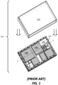
- FIG. 1 illustrates an integrated device 100 that includes a printed circuit board (PCB) 102, a first integrated circuit (IC) package 104, a second integrated circuit (IC) package 106, a passive component 108 (e.g., capacitor), and a cover 130.
- the first integrated circuit (IC) package 104, the second integrated circuit (IC) package 106, and the passive component 108 are coupled to the printed circuit board (PCB) 102.
- the cover 130 is coupled to the printed circuit board (PCB) 102.
- the cover 130 may be a metallic material that covers and protects the first integrated circuit (IC) package 104, the second integrated circuit (IC) package 106, and the passive component 108, from an external environment.
- the use of the cover 130 results in a void in the integrated device 100.
- This wasted space in the integrated device 100 limits how small the integrated device 100 can be, which in turns, limits the type of devices in which the integrated device may be implemented.
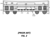
- FIG. 2 illustrates an example of such a defect when ICs are packed close together.
- FIG. 2 illustrates a package on package (PoP) device 200 that includes a first package 202, a second package 204 and a void 290.
- the first package 202 includes a first die 220, a first package substrate 222, and a first encapsulation layer 250.
- the first package substrate 222 includes a first plurality of pads 224 and a first pad 226.
- the first die 220 is coupled to the first package substrate 222 through a first plurality of solder balls 228. Specifically, the first die 220 is coupled to the first plurality of pads 224 through the first plurality of solder balls 228.
- a second plurality of solder balls 236 is coupled to the first package substrate 222.
- the second package 204 includes a second die 240, a second package substrate 242, a second pad 246, a third plurality of solder balls 256, and a second encapsulation layer 260.
- the second die 240 is coupled to the second package substrate 242.
- the second package 204 is coupled to the first package 202 through the third plurality of solder balls 256.
- the third plurality solder balls 256 is coupled to the first pad 226 of the first package substrate 222, and the second pad 246 of the second package 204.
- FIG. 2 illustrates a void 290 between the first die 220 and the second package substrate 242 of the second package 204.
- the void 290 is a space in the first encapsulation layer 250.
- the void 290 may occur when the gap or space between the first die 220 and the second package substrate 242 is too small or narrow to allow the first encapsulation layer 250 to completely flow in between the first die 220 and the second package substrate 242.
- the presence of the void 290 can cause warpage and/or deformation (as illustrated by the arrow) in the package on package (PoP) device 200 because of the lack of structural support around that space.
- warpage and/or deformation are the weak joints and/or open joints that may occur between the third plurality of solder balls 256 and the first pad 226 and the second pad 246. For example, as shown in FIG.
- the warpage and/or deformation of the package on package device (PoP) 200 causes increased separation between the first pad 226 and the second pad 246, which effectively stretches the third plurality of solder balls 256 (as illustrated by the arrow), and results in a weaker joint and/or open joint in the package on package (PoP) device 200.
- a weak joint and/or an open joint can prevent signals from properly traversing through a package on package (PoP) device, resulting in a defective package on package (PoP) device.
- the gap or space between the first die 220 and the second package substrate 242 has to increase, which effectively increases the size of the package on package (PoP) device 200, which is not desirable.
- US 2015/237713 A1 discusses an apparatus including a first substrate, a die having interconnect structures coupled with the first substrate to route input/output (I/O) signals between the die and the first substrate and a second substrate coupled with the first substrate, wherein the die is disposed between the first substrate and the second substrate and at least one of the first substrate and the second substrate include traces.
- I/O input/output
- US 2003/038355 A1 discusses a semiconductor device including at least one nonconfluent spacer layer on at least one surface thereof.
- the at least one nonconfluent spacer layer at least partially spaces the surface of the semiconductor device apart from another semiconductor device assembled in stacked arrangement therewith.
- Adjacent stacked semiconductor devices may include abutting nonconfluent spacer layers which together define a distance between opposed surfaces of the semiconductor devices.
- US 2010/327419 A1 discusses a stacked-chip apparatus including a package substrate and an interposer with a chip stack disposed with a standoff that matches the interposer.
- EP 2701191 A2 discusses arranging a plurality of microelectronic device panels in a panel stack.
- Each microelectronic device panel contains a plurality of microelectronic devices and a plurality of package edge conductors extending therefrom. Trenches are created in the panel stack exposing the plurality of package edge conductors, and a plurality of sidewall conductors is formed interconnecting different ones of the package edge conductors exposed through the trenches.
- the panel stack is then separated into a plurality of stacked microelectronic packages each including at least two microelectronic devices electrically interconnected by at least one of the plurality of sidewall conductors included within the stacked microelectronic package.
- TW 201521164 A discusses a package on package structure comprising a first package substrate, an electronic element disposed on the first package substrate, a second package substrate stacked on the first package substrate via a support member, and a package colloid provided between the first and the second package substrates for coating the electronic element and the support member, the second package substrate has a plurality of electrical contact pads and at least one groove, and the groove is closer to the edge of the second package substrate compared to the electrical contact pads.
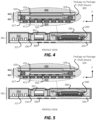
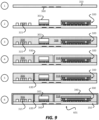
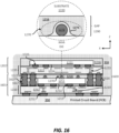
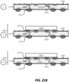
- FIG. 3 illustrates an integrated device 301 that includes a package on package (PoP) device 300, the packages 302-311, a passive component 315, an encapsulation layer 316, an internal shield 330, an external shield 340, and a printed circuit board (PCB) 350.
- the integrated device 301 may include a System in Package (SiP).
- One or more of the packages 302-311 may include an integrated circuit (IC) package.
- the one or more packages 302-311 may be examples of electronic package components.
- the package on package (PoP) device 300, the packages 302-311, the passive component 315 (e.g., capacitor), the internal shield 430, and the external shield 440 are coupled to the printed circuit board (PCB) 350.
- the encapsulation layer 316 may partially or completely encapsulate or cover the package on package (PoP) device 300, the packages 302-311, the passive component 315, and the internal shield 330 in various ways. Although provided as a single system in a package, these components may be isolated from each other mechanically and/or electrically.
- FIG. 3 illustrates that the internal shield 330 may be configured to surround one or more packages 302-311 and/or the package on package (PoP) device 300.
- the internal shield 330 is configured to isolate one or more packages 302-311 and/or the package on package (PoP) device 300 so that they don't interfere with one another.
- a package e.g., package 302-311) may include a die or may be a die (e.g., semiconductor device).
- a package (e.g., package 302-311) may include a wafer level package (WLP).
- WLP wafer level package
- the encapsulation layer 316 serves as a covering or protective structure for the components of the device 300.
- the encapsulation layer 316 may be a molding compound having various viscosities and thermal properties. Those skilled in the art will recognize that other types of materials may be used in the encapsulation layer 316.
- the external shield 340 is configured to at least partially surround the encapsulation layer 316.
- the external shield 340 is coupled to the internal shield 330.
- the combination of the internal shield 330 and the external shield 340 may provide shielding for the integrated device 301.
- the internal shield 330 and the external shield 340 may include a conductive material (e.g., metal, copper).
- the internal shield 330 and the external shield 340 may have the same material or be different materials.
- the internal shield 330 may include a metal sheet in some implementations.
- the internal shield 330 has a thickness of about 250 microns ( ⁇ m) or less.
- the external shield 340 has a thickness of about 50 microns ( ⁇ m) or less.
- the integrated device 301 may include any component that is configured to provide several mobile functionalities and capabilities, including but not limited to, positioning functionality, wireless connectivity functionality (e.g., wireless communication) and/or cellular connectivity functionality (e.g., cellular communication).
- positioning functionality, wireless and/or cellular connectivity functionalities include global positioning system (GPS) functionality, wireless fidelity (WiFi) functionality, Bluetooth functionality, and radio frequency (RF) functionality (e.g., Radio Frequency Front End (RFFE) functionality).
- GPS global positioning system
- WiFi wireless fidelity
- RFFE radio frequency
- Examples of RFFE functionalities include Global System for Mobile Communications (GSM), Wideband Code Division Multiple Access (WCDMA), Frequency Division Duplex Long-Term Evolution (FDD-LTE), Time Division Duplex Long-Term Evolution (TDD-LTE).
- GSM Global System for Mobile Communications
- WCDMA Wideband Code Division Multiple Access
- FDD-LTE Frequency Division Duplex Long-Term Evolution
- TDD-LTE Time Division Duplex Long-Term
- FIG. 3 further illustrates the integrated device 301 may include an embedded package on package (PoP) device 300.
- PoP package on package
- embedding the package on package (PoP) device 300 with the integrated device 301 provides an integrated device with an overall form factor (e.g., size, area, volume) that is smaller than other conventional integrated devices, while providing an integrated device that includes a comprehensive, full and/or complete range of mobile functionalities. Exemplary sizes for integrated devices with such mobile functionalities are further described below in FIG. 11 .
- the integrated device 301 that includes at least some of the above mobile functionalities (e.g., cellular functionality, wireless fidelity (WiFi) functionality and Bluetooth functionality) is made possible through the structures and/or fabrication processes described in the present application.
- fabricating an integrated device e.g., integrated device 301 with many mobile functionalities, a small form factor, and that is encapsulated in an encapsulation layer (e.g., fully encapsulated by an encapsulation layer) includes many fabrication and manufacturing challenges that are addressed in the present application. In particular, as the size and spacing between components in an integrated device becomes smaller, defects appears, which causes performance and reliability issues in the integrated device.
- FIG. 3 further illustrates an example of an integrated device 301 that is hermetically sealed through the use of one or more encapsulation layer(s), which helps improve the reliability and durability of the integrated device 301.
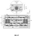
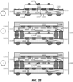
- FIG. 4 illustrates a profile view of the integrated device 301.
- the integrated device 301 includes the printed circuit board (PCB) 350, the package on package (PoP) device 300, the package 302, the passive component 315, the encapsulation layer 316 (e.g., second encapsulation layer),, the internal shield 330, and the external shield 340.
- the printed circuit board (PCB) 350 includes a plurality of interconnects 360 (e.g., pads).
- the package on package (PoP) device 300, the package 302, the passive component 315, the internal shield 330 and the external shield 340 are coupled to the printed circuit board (PCB) 350.
- the encapsulation layer 316 at least partially encapsulates the package on package (PoP) device 300, the package 302, the passive component 315 and the internal shield 330.
- the package on package (PoP) device 300 includes a first package 401, a second package 402, and a first encapsulation layer 416.
- the second package 402 is coupled to the first package 401 through a plurality of package interconnects 427.
- the plurality of package interconnects 427 includes a solder interconnect (e.g., solder ball).
- the first package 401 includes a first package substrate 410 and a first die 411.
- the second package 402 includes a second package substrate 420 and a second die 421.
- the first encapsulation layer 416 is formed between the first package 401 and the second package 402.
- the first encapsulation layer 416 is at least formed between the first die 411 (e.g., back side surface of the first die 411) and the second package substrate 420 (e.g., bottom surface of second package substrate 420).
- FIG. 4 illustrates that the encapsulation layer 316 and the first encapsulation layer 416 are separate encapsulation layers.
- the encapsulation layer that encapsulates the package on package (PoP) device 300 may be the same encapsulation layer that is formed in the package on package (PoP) device 300.
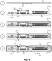
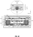
- FIG. 5 illustrates the integrated device 501 that includes a package on package (PoP) device.
- the integrated device 501 of FIG. 5 is similar to the integrated device 301 of FIG. 4 , except that the package on package (PoP) device 500 is embedded differently in the integrated device 501.
- PoP package on package
- the package on package (PoP) device 500 includes a first package 401 and a second package 402.
- the first package 401 includes the first package substrate 410 and the first die 411.
- the second package 402 is coupled to the first package 401 through the plurality of package interconnects 427.
- the encapsulation layer 316 at least partially encapsulates the package on package (PoP) device 500, and is formed between the first package 401 and the second package 402.
- the encapsulation layer 316 is at least formed between the first die 411 (e.g., back side surface of the first die 411) and the second package substrate 420 (e.g., bottom surface of second package substrate 420).
- providing an encapsulation layer that both encapsulates and embeds the package on package (PoP) device 500 may enable an integrated device 501 that is low cost and has a small form factor, as it may reduce the number of processes to fabricate the integrated device.
- FIG. 6 illustrates an integrated device 601 that includes a package on package (PoP) device.
- the integrated device 601 of FIG. 6 is similar to the integrated device 301 of FIG. 4 , except that the integrated device 601 may comprise an internal shield 630 that is different than the internal shield 330 of the integrated device 301.
- the internal shield 630 may be thinner than the internal shield 330.
- the internal shield 630 is formed using a different process than the internal shield 330.
- the internal shield 330 may include a metal sheet that has been worked to form a desired shape and then coupled to the printed circuit board (PCB) 350 with solder or some other conductive mechanism.
- PCB printed circuit board
- the internal shield 630 may be a metal layer (e.g., copper layer) that is formed (e.g., deposited, pasted) in a cavity of the encapsulation layer 316.
- the internal shield 630 is coupled to the external shield 340 and the printed circuit board (PCB) 350.
- PCB printed circuit board
- FIG. 7 illustrates an integrated device 701 that includes a package on package (PoP) device.
- the integrated device 701 of FIG. 7 is similar to the integrated device 601 of FIG. 6 , except that the package on package (PoP) device 500 is embedded differently in the integrated device 701.
- PoP package on package
- the package on package (PoP) device 500 includes a first package 401 and a second package 402.
- the first package 401 includes the first package substrate 410 and the first die 411.
- the second package 402 is coupled to the first package 401 through the plurality of package interconnects 427.
- the encapsulation layer 316 at least partially encapsulates the package on package (PoP) device 500, and is formed between the first package 401 and the second package 402.
- the encapsulation layer 316 is at least formed between the first die 411 (e.g., back side surface of the first die 411) and the second package substrate 420 (e.g., bottom surface of second package substrate 420).
- providing an encapsulation layer that both encapsulates and embeds the package on package (PoP) device 500 may enable an integrated device 701 that is low cost and has a small form factor, as it may reduce the number of processes to fabricate the integrated device.
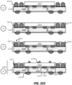
- Stage 1 illustrates a state after a printed circuit board (PCB) 350 that includes a plurality of interconnects 360 is provided.
- the printed circuit board (PCB) 350 is provided by a supplier or fabricated.
- Stage 5 illustrates a state after the external shield 340 is formed over the encapsulation layer 316.
- the external shield 340 may be formed using various materials, such as a conductive paste, copper or other conductive metals, and the like.
- the external shield 340 is coupled to the internal shield 330 and the printed circuit board (PCB) 350.
- stage 5 illustrates the integrated device 601 that includes the package on package (PoP) device 500, the package 302, the passive component 315, the internal shield 330, the solder interconnect 332, the encapsulation layer 316, the printed circuit board (PCB) 350, and the external shield 340.
- PoP package on package
- PCB printed circuit board
- Stage 2 illustrates the package on package (PoP) device 300 and the passive component 315 coupled to the printed circuit board (PCB) 350.
- a solder reflow process is used to couple the package on package (PoP) device 300 and the passive component 315 (e.g., through the use of solder interconnects) to the printed circuit board (PCB) 350.
- Stage 3 illustrates the encapsulation layer 316 at least partially formed over the package on package (PoP) device 300 and the passive component 315.
- Stage 5 illustrates the cavity 930 filled with a conductive material to form the internal shield 630.
- Different implementations may use different processes for forming the internal shield 630.
- a pasting process, a plating process, and/or a sputtering process may be used to fill the cavity 930 to form the internal shield 630.
- a package on package (PoP) device e.g., 300
- at least one package e.g., 302
- an internal shield e.g., 330
- PCB printed circuit board
- Examples of coupling a package on package (PoP) device, at least one package, and an internal shield to a printed circuit board (PCB) are illustrated and described in FIG. 8 (e.g., stage 2 of FIG. 8 ).
- a solder reflow process may be used to couple a package on package (PoP) device, at least one package, and an internal shield to (e.g., through a plurality of solder interconnects) a printed circuit board (PCB).
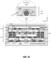
- one or more of the gap controller 1270 may occupy less than substantially all of a space between a first die (e.g., first die 1211) and a second package (e.g., second package 1202). In some implementations, one or more of the gap controller 1270, individually or collectively, is coupled to less than substantially all of a back side surface of a first die (e.g., first die 1211). In some implementations, one or more of the gap controller 1270, individually or collectively, is coupled to less than a majority of a back side surface of a first die (e.g., first die 1211).
- the distance, space or gap between the first die 1211 (e.g., top surface of the first die 1211) and the second package 1202 (e.g., bottom surface of the second package substrate 1220) may vary with different implementations.
- the gap 1290 may be about 10 microns ( ⁇ m) or more.
- the gap controller 1270 has a height of about 10-100 microns ( ⁇ m) or less.
- the gap controller 1270 ensures that the minimum gap (e.g., gap 1290) between the first die 1211 (e.g., back side surface of the first die 1211) and the second package 202 (e.g., bottom surface of the second package substrate 1220) is about 10 microns ( ⁇ m) or greater.
- the gap controller 1270 eliminates, reduces and/or minimizes a void between the first die 1211 and the second package substrate 1220, thereby providing a more robust and reliable package on package (PoP) device 1200.
- the gap controller 1270 is configured to allow the first encapsulation layer 1216 to fill the space (e.g., to at least fill a majority or a substantial part of the space) between the first die 1211 and the second package substrate 1220.
- the gap controller 1270 is configured to not substantially impede the flow of the first encapsulation layer 1216 (e.g., during a fabrication process), when the first encapsulation layer 1216 is formed.
- the use of one or more of the gap controller 1270 provides an effective and counter intuitive approach to ensure that the first encapsulation layer 1216 can flow between the first die 1211 and the second package substrate 1220, during a fabrication process of the package on package (PoP) device 1200.
- PoP package on package
- the gap controller 1270 positions the gap controller 1270 over different portions of the first die 1211.
- the greatest amount of warpage, deformation, and/or deflection of the second package substrate 1220 may occur in a space above a center of the first die 1211, a center of the first package 1201 and/or a center of the second package 1202.
- the gap controller 1270 positioned on or about (e.g., near) a center of the first die 1211, to ensure that there is support in a portion of the second package substrate 1220 that may potentially have the greatest amount of warpage, deformation and/or deflection.
- FIG. 12 illustrates that the gap controller 1270 includes a spacer 1272 and an adhesive layer 1274.
- the adhesive layer 1274 at least partially surrounds the spacer 1272. Different implementations may use different materials for the spacer 1272 and the adhesive layer 1274.
- the spacer 1272 may be a metal ball (e.g., copper ball).
- the adhesive layer 1274 may be used to couple the spacer 1272 to the first die 1211.
- the adhesive layer 1274 may be configured to prevent the gap controller 1270 from substantially moving when the first encapsulation layer 1216 is formed between the first die 1211 and the second package 1202.
- the spacer 1272 may include a solid spacer that includes a ceramic, a metal, and/or a polymer (e.g., copper, a polymer core ball and/or polymer post).
- the adhesive layer 1274 may include an underfill and/or a high viscosity comer fill material (e.g., Cookson HEL-30, Namics G8345D) and RTV silicon (e.g., ASE 600).
- the adhesive layer 1274 may include a sintering paste (e.g., Ormet 406, CS650).
- the first encapsulation layer 1216 at least partially surrounds the adhesive layer 1274 and the spacer 1272.
- FIG. 12 also illustrates that the gap controller 1270 is in direct physical contact with the first die 1211, but not in direct physical contact with the second package 1202 (e.g., second package substrate 1220 of the second package 1202).
- the gap controller 1270 may be in direct physical contact with both the first die 1211 and the second package 1202 (e.g., second package substrate 1220 of the second package 1202).
- the gap controller 1270 may be in direct physical contact with the second package 1202 (e.g., second package substrate 1220 of the second package 1202), but not in direct contact with the first die 1211.
- solder balls e.g., 1215, 1225
- the dies e.g., 1211, 1221
- the package substrates e.g., 1210, 1220
- other interconnects may be used to couple the dies to the package substrates.
- some implementations may use wire bonding and pillars (e.g., copper pillars) to couple dies to a package substrate.
- PoP Package on Package
- the gap controller 1270 is configured to ensure that there is enough distance, space or gap between a die of the first package 1801, and a package substrate of the second package 1202, so that an encapsulation layer can be provided (e.g., formed) in the space or the gap between the die of the first package 1801, and the package substrate of the second package 1202.
- the encapsulation layer 1816 at least partially encapsulates the first die 1811 and the plurality of package interconnects 1827.
- the encapsulation layer 1816 at least partially encapsulates the first die 1811 and the plurality of package interconnects 1817.
- a surface of the encapsulation layer 1816 may be substantially co-planar with a surface (e.g., back side surface) of the first die 1811.
- the first encapsulation layer 1216 is formed over the first die 1811 and the encapsulation layer 1816.
- the encapsulation layer 1816 may be the same material or a different material as the first encapsulation layer 1216.
- the first encapsulation layer 1216 at least partially encapsulates the gap controller 1270 and the plurality of package interconnects 1827.
- the second package 1202 is coupled to the first package 1801 through the plurality of package interconnects 1827, which includes the plurality of package interconnects 1227 and the plurality of package interconnects 1817.
- the plurality of package interconnects 1827 may include a solder interconnect (e.g., solder ball).
- the plurality of package interconnects 1827 is coupled to the first redistribution portion 1810 and the second package substrate 1220.
- the plurality of package interconnects 1827 is coupled to the at least one redistribution layer 1815 (of the first redistribution portion 1810) and the plurality of second interconnects 1223 (of the second package substrate 1220).
- the plurality of package interconnects 1227 is coupled to the plurality of second interconnects 1223 and the plurality of package interconnects 1817.
- the plurality of package interconnects 1817 is coupled to the at least one redistribution layer 1815 of the first redistribution portion 1810.
- FIG. 18 illustrates that the package on package (PoP) device 1800 is at least partially encapsulated by the encapsulation layer 316.
- the encapsulation layer 316 may be distinct and separate from the first encapsulation layer 1216 in some embodiments. In some implementations not forming part of the present invention but useful for understanding it, the encapsulation layer 316 may include the first encapsulation layer 1216. In some implementations not forming part of the present invention but useful for understanding it, the encapsulation layer 316 is the same as the first encapsulation layer 1216.
- the encapsulation layer 316 may both encapsulate the package on package (PoP) device 1800 and be located inside the package on package (PoP) device 1800.
- the above concept is illustrated in FIG. 18 by the dashed boundary (e.g., line) between the encapsulation layer 316 and the first encapsulation layer 1216.
- the gap controller 1270 is located over the first die 1811 (e.g., back side of the first die 1811). In particular, the gap controller 1270 is located between the first die 1811 of the first package 1801, and the second package substrate 1220 of the second package 1202. In some implementations, the gap controller 1270 is configured to provide a minimum distance, a minimum space, and/or a minimum gap between the first die 1811 of the first package 1801, and the second package substrate 1220 of the second package 1202.
- the minimum distance, the minimum space, the minimum gap ensures that there is enough room for the first encapsulation layer 1216 to flow (e.g., during a fabrication process) between the first die 1811 of the first package 1801, and the second package substrate 1220 of the second package 1202, even when there is warpage, deformation, and/or deflection of the second package substrate 1220.
- at least one gap controller 1270 that is located over the first die 1811 e.g., over a back side of the first die 1811 ensures that a sufficient amount of the first encapsulation layer 1216 is formed between the first die 1811 and the second package substrate 1220 (of the second package 1202).
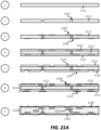
- FIG. 21 illustrates sequence for providing / fabricating a package that includes a gap controller according to the present invention.
- the sequence of FIGS. 21A-21C may be used to fabricate the package (e.g., integrated circuit (IC) package) that includes a gap controller of FIGS. 12 and 16-19 and/or other packages described in the present disclosure.
- FIGS. 21A-21C will be described in the context of providing / fabricating a package of FIG. 16 .
- FIGS. 21A-21C will be described in the context of fabricating the first package 1601 of FIG. 16 .
- Stage 5 illustrates at least one cavity 2105 formed in the second dielectric layer 2122, and at least one cavity 2107 formed in the third dielectric layer 2132.
- Different implementations may form the cavity 2105 in the second dielectric layer 2122 and the cavity 2107 in the third dielectric layer 2132 differently.
- a laser process and/or a photo-lithography process may be used to form the cavity 2105 and/or the cavity 2107.
- Stage 6 illustrates a third metal layer 2108 formed on and/or in the second dielectric layer 2122, a fourth metal layer 2110 formed on and/or in the third dielectric layer 2132.
- the third metal layer 2108 and the fourth metal layer 2110 may represent the plurality of first interconnects 1213, as described above in at least FIG. 16 .
- Stage 6 may represent a package substrate (e.g., first package substrate 1210) that includes at least one dielectric layer and a plurality of first interconnects.
- Stage 7 illustrates a first solder resist layer 1280 formed over the dielectric layer 1212, and a second solder resist layer 1282 formed over the dielectric layer 1212.
- the dielectric layer 1212 may collectively represent the first dielectric layer 2112, the second dielectric layer 2122, and the third dielectric layer 2132.
- Stage 7 may represent a package substrate (e.g., first package substrate 1210) that includes the dielectric layer 1212, the plurality of first interconnects 1213, the first solder resist layer 1280, and the second solder resist layer 1282.
- Stage 8 illustrates the plurality of solder balls 1251 coupled to the first package substrate 1210.
- the plurality of solder balls 1252 is coupled to the plurality of first interconnects 1213.
- Stage 9 illustrates the first die 1211 coupled to the first package substrate 1210, through the plurality of first solder balls 1215.
- Different implementations may couple the first die 1211 to the first package substrate 1210 differently (e.g., by using interconnect pillars).
- a reflow process e.g., chip attach reflow process
- a reflux process may be used after the reflow process.
- Stage 10 illustrates a first underfill 1214 provided between the first die 1211 and the first package substrate 1210.
- the first underfill 1214 may at least partially surround the plurality of first solder balls 1215.
- providing the first underfill 1214 includes an underfill dispense process.
- Stage 11 illustrates a plurality of package interconnects 1617 provided (e.g., formed) over the first package substrate 1210.
- the plurality of package interconnects 1617 may include a solder interconnect.
- Stage 12 illustrates an encapsulation layer 1616 at least partially formed over the first die 1211, the first package substrate 1210, and the plurality of package interconnects 1617.
- the encapsulation layer 1616 at least partially encapsulates the first die 1211 and the plurality of package interconnects 1617.
- the first die 1211 is completely encapsulated by the encapsulation layer 1616 and the encapsulation layer 1616 is grinded down such that a top surface of the encapsulation layer 1616 is substantially co-planar with a surface (e.g., back side surface) of the first die 1211.
- Stage 13 illustrates at least one cavity 2116 formed in the encapsulation layer 1616.
- the cavity 2116 may be formed to at least partially expose the plurality of package interconnects 1617.
- a laser process and/or a photo-lithography process may be used to form the cavity 2116.
- Stage 14 illustrates at least one gap controller 1270 coupled to the first die 1211 (e.g., to the back side surface of the first die 1211).
- Stage 14 illustrates in some implementations, a first package 1601 that includes a first package substrate 1210, a first die 1211, a plurality of package interconnects 1617, an encapsulation layer 1616, and at least one gap controller 1270.
- the at least one gap controller 1270 is deposited on the first die 1211.
- first packages are concurrently fabricated on wafer, and a singulation process is performed to cut a wafer into individual packages.
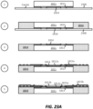
- a first integrated circuit (IC) package that includes a first electronic package component (e.g., first die) is formed. Examples of forming a first integrated circuit (IC) package are illustrated and described in FIGS. 21A-21C and 23A-23B.
- the first integrated circuit (IC) package may include a fan out wafer level package (FOWLP).
- the first integrated circuit (IC) package may include a package substrate or a redistribution portion.
- the first integrated circuit (IC) package may include an encapsulation layer. Examples of a first package (e.g., first integrated circuit (IC) package) include the first package 1201, the first package 1601, the first package 1701, the first package 1801, and the first package 2001.
Landscapes
- Engineering & Computer Science (AREA)
- Microelectronics & Electronic Packaging (AREA)
- Power Engineering (AREA)
- Computer Hardware Design (AREA)
- Physics & Mathematics (AREA)
- Condensed Matter Physics & Semiconductors (AREA)
- General Physics & Mathematics (AREA)
- Manufacturing & Machinery (AREA)
- Computer Networks & Wireless Communication (AREA)
- Signal Processing (AREA)
- Health & Medical Sciences (AREA)
- Electromagnetism (AREA)
- Toxicology (AREA)
- Structures Or Materials For Encapsulating Or Coating Semiconductor Devices Or Solid State Devices (AREA)
- Casings For Electric Apparatus (AREA)
- Shielding Devices Or Components To Electric Or Magnetic Fields (AREA)
- Structure Of Printed Boards (AREA)
- Production Of Multi-Layered Print Wiring Board (AREA)
- Transceivers (AREA)
Applications Claiming Priority (3)
| Application Number | Priority Date | Filing Date | Title |
|---|---|---|---|
| US201562236766P | 2015-10-02 | 2015-10-02 | |
| US15/097,719 US10163871B2 (en) | 2015-10-02 | 2016-04-13 | Integrated device comprising embedded package on package (PoP) device |
| PCT/US2016/054021 WO2017058825A1 (en) | 2015-10-02 | 2016-09-27 | INTEGRATED DEVICE COMPRISING EMBEDDED PACKAGE ON PACKAGE (PoP) DEVICE |
Publications (3)
| Publication Number | Publication Date |
|---|---|
| EP3357088A1 EP3357088A1 (en) | 2018-08-08 |
| EP3357088C0 EP3357088C0 (en) | 2025-07-09 |
| EP3357088B1 true EP3357088B1 (en) | 2025-07-09 |
Family
ID=57138130
Family Applications (1)
| Application Number | Title | Priority Date | Filing Date |
|---|---|---|---|
| EP16782134.7A Active EP3357088B1 (en) | 2015-10-02 | 2016-09-27 | Integrated device comprising embedded package on package, pop, device |
Country Status (9)
Families Citing this family (34)
| Publication number | Priority date | Publication date | Assignee | Title |
|---|---|---|---|---|
| US9627367B2 (en) * | 2014-11-21 | 2017-04-18 | Micron Technology, Inc. | Memory devices with controllers under memory packages and associated systems and methods |
| US10163871B2 (en) | 2015-10-02 | 2018-12-25 | Qualcomm Incorporated | Integrated device comprising embedded package on package (PoP) device |
| US9721903B2 (en) * | 2015-12-21 | 2017-08-01 | Apple Inc. | Vertical interconnects for self shielded system in package (SiP) modules |
| US10631410B2 (en) * | 2016-09-24 | 2020-04-21 | Apple Inc. | Stacked printed circuit board packages |
| KR20190067839A (ko) * | 2016-10-04 | 2019-06-17 | 스카이워크스 솔루션즈, 인코포레이티드 | 오버몰드 구조를 갖는 양면 라디오-주파수 패키지 |
| US10475770B2 (en) * | 2017-02-28 | 2019-11-12 | Amkor Technology, Inc. | Semiconductor device having stacked dies and stacked pillars and method of manufacturing thereof |
| TWI699840B (zh) * | 2017-10-23 | 2020-07-21 | 美商應用材料股份有限公司 | 形成扇出互連結構與互連結構的方法 |
| TWI640068B (zh) | 2017-11-30 | 2018-11-01 | 矽品精密工業股份有限公司 | 電子封裝件及其製法 |
| KR101942748B1 (ko) | 2018-01-31 | 2019-01-28 | 삼성전기 주식회사 | 팬-아웃 반도체 패키지 |
| US10896880B2 (en) | 2018-11-28 | 2021-01-19 | Shiann-Tsong Tsai | Semiconductor package with in-package compartmental shielding and fabrication method thereof |
| US11211340B2 (en) | 2018-11-28 | 2021-12-28 | Shiann-Tsong Tsai | Semiconductor package with in-package compartmental shielding and active electro-magnetic compatibility shielding |
| US10923435B2 (en) | 2018-11-28 | 2021-02-16 | Shiann-Tsong Tsai | Semiconductor package with in-package compartmental shielding and improved heat-dissipation performance |
| US11239179B2 (en) | 2018-11-28 | 2022-02-01 | Shiann-Tsong Tsai | Semiconductor package and fabrication method thereof |
| US10867947B2 (en) * | 2018-11-29 | 2020-12-15 | Taiwan Semiconductor Manufacturing Company, Ltd. | Semiconductor packages and methods of manufacturing the same |
| TWI720749B (zh) * | 2019-01-01 | 2021-03-01 | 蔡憲聰 | 具有封裝內隔室屏蔽的半導體封裝及其製作方法 |
| KR102717843B1 (ko) | 2019-08-02 | 2024-10-16 | 삼성전자주식회사 | 반도체 패키지 및 그의 제조 방법 |
| US20220246597A1 (en) * | 2019-08-29 | 2022-08-04 | Showa Denko Materials Co., Ltd. | Method for manufacturing electronic component device and electronic component device |
| WO2021075035A1 (ja) * | 2019-10-17 | 2021-04-22 | 日本電信電話株式会社 | 光通信部品 |
| CN111162755B (zh) * | 2020-01-16 | 2021-09-21 | 诺思(天津)微系统有限责任公司 | 一种体声波双工滤波器 |
| DE102021100220B4 (de) | 2020-01-21 | 2024-06-13 | Taiwan Semiconductor Manufacturing Co., Ltd. | Package-Struktur und deren Herstellungsverfahren |
| KR20210099947A (ko) * | 2020-02-05 | 2021-08-13 | 삼성전기주식회사 | 칩 고주파 패키지 및 고주파 모듈 |
| US20210280507A1 (en) * | 2020-03-05 | 2021-09-09 | Qualcomm Incorporated | Package comprising dummy interconnects |
| KR102124769B1 (ko) * | 2020-03-13 | 2020-06-23 | (주)일신이디아이 | 무선통합시스템용 광대역 안테나 유닛 |
| CN111415913B (zh) * | 2020-04-09 | 2021-10-01 | 环维电子(上海)有限公司 | 一种具有电磁屏蔽结构的选择性封装sip模组及其制备方法 |
| US12055633B2 (en) * | 2020-08-25 | 2024-08-06 | Lumentum Operations Llc | Package for a time of flight device |
| CN112885794B (zh) * | 2021-01-15 | 2023-04-07 | 浪潮电子信息产业股份有限公司 | 一种pcb、pop封装散热结构及其制造方法 |
| US11985804B2 (en) | 2021-07-22 | 2024-05-14 | Qualcomm Incorporated | Package comprising a block device with a shield and method of fabricating the same |
| US11869848B2 (en) | 2021-08-11 | 2024-01-09 | STATS ChipPAC Pte. Ltd. | Semiconductor device and method of stacking devices using support frame |
| KR20230028653A (ko) * | 2021-08-20 | 2023-03-02 | 삼성전자주식회사 | 반도체 패키지 및 제조방법 |
| KR20230045660A (ko) | 2021-09-27 | 2023-04-05 | 삼성전자주식회사 | 반도체 패키지 |
| WO2023157747A1 (ja) * | 2022-02-16 | 2023-08-24 | 株式会社村田製作所 | 回路モジュール |
| WO2023157748A1 (ja) * | 2022-02-16 | 2023-08-24 | 株式会社村田製作所 | 回路モジュール |
| US12183687B2 (en) | 2022-04-06 | 2024-12-31 | STATS ChipPAC Pte. Ltd. | Semiconductor device and method using an EMI-absorbing metal bar |
| CN118315374B (zh) * | 2024-06-11 | 2024-10-29 | 甬矽电子(宁波)股份有限公司 | 芯片堆叠结构和芯片封装方法 |
Citations (1)
| Publication number | Priority date | Publication date | Assignee | Title |
|---|---|---|---|---|
| US20070013060A1 (en) * | 2004-05-24 | 2007-01-18 | Chippac, Inc | Stacked Semiconductor Package having Adhesive/Spacer Structure and Insulation |
Family Cites Families (37)
| Publication number | Priority date | Publication date | Assignee | Title |
|---|---|---|---|---|
| JP3668074B2 (ja) * | 1999-10-07 | 2005-07-06 | 松下電器産業株式会社 | 半導体装置およびその製造方法 |
| US7518223B2 (en) | 2001-08-24 | 2009-04-14 | Micron Technology, Inc. | Semiconductor devices and semiconductor device assemblies including a nonconfluent spacer layer |
| TW529141B (en) * | 2002-01-07 | 2003-04-21 | Advanced Semiconductor Eng | Stacking type multi-chip package and its manufacturing process |
| US7053476B2 (en) * | 2002-09-17 | 2006-05-30 | Chippac, Inc. | Semiconductor multi-package module having package stacked over die-down flip chip ball grid array package and having wire bond interconnect between stacked packages |
| US20040061213A1 (en) * | 2002-09-17 | 2004-04-01 | Chippac, Inc. | Semiconductor multi-package module having package stacked over die-up flip chip ball grid array package and having wire bond interconnect between stacked packages |
| JP4012987B2 (ja) * | 2002-10-04 | 2007-11-28 | 株式会社村田製作所 | モジュール基板の段積み構造 |
| US7116002B2 (en) | 2004-05-10 | 2006-10-03 | Taiwan Semiconductor Manufacturing Company, Ltd. | Overhang support for a stacked semiconductor device, and method of forming thereof |
| JP4383324B2 (ja) * | 2004-11-10 | 2009-12-16 | Necエレクトロニクス株式会社 | 半導体装置 |
| KR100698527B1 (ko) | 2005-08-11 | 2007-03-22 | 삼성전자주식회사 | 금속 범프를 이용한 기둥 범프를 구비하는 칩 적층 패키지및 그의 제조방법 |
| JP5116268B2 (ja) * | 2005-08-31 | 2013-01-09 | キヤノン株式会社 | 積層型半導体装置およびその製造方法 |
| JP4182140B2 (ja) * | 2005-12-14 | 2008-11-19 | 新光電気工業株式会社 | チップ内蔵基板 |
| US7573137B2 (en) * | 2006-03-31 | 2009-08-11 | Texas Instruments Incorporated | Controlling flip-chip techniques for concurrent ball bonds in semiconductor devices |
| US7569918B2 (en) * | 2006-05-01 | 2009-08-04 | Texas Instruments Incorporated | Semiconductor package-on-package system including integrated passive components |
| KR100784498B1 (ko) | 2006-05-30 | 2007-12-11 | 삼성전자주식회사 | 적층 칩과, 그의 제조 방법 및 그를 갖는 반도체 패키지 |
| JP2008091638A (ja) | 2006-10-02 | 2008-04-17 | Nec Electronics Corp | 電子装置およびその製造方法 |
| TWI342603B (en) | 2006-11-22 | 2011-05-21 | Advanced Semiconductor Eng | Package assembly whose spacer has through hole |
| US7923830B2 (en) * | 2007-04-13 | 2011-04-12 | Maxim Integrated Products, Inc. | Package-on-package secure module having anti-tamper mesh in the substrate of the upper package |
| US7863090B2 (en) * | 2007-06-25 | 2011-01-04 | Epic Technologies, Inc. | Packaged electronic modules and fabrication methods thereof implementing a cell phone or other electronic system |
| US20090051046A1 (en) * | 2007-08-24 | 2009-02-26 | Semiconductor Energy Laboratory Co., Ltd. | Semiconductor device and manufacturing method for the same |
| JP5324191B2 (ja) * | 2008-11-07 | 2013-10-23 | ルネサスエレクトロニクス株式会社 | 半導体装置 |
| US20100327419A1 (en) | 2009-06-26 | 2010-12-30 | Sriram Muthukumar | Stacked-chip packages in package-on-package apparatus, methods of assembling same, and systems containing same |
| EP2460180B1 (en) | 2009-07-30 | 2020-02-19 | QUALCOMM Incorporated | System-in packages |
| US9437512B2 (en) * | 2011-10-07 | 2016-09-06 | Mediatek Inc. | Integrated circuit package structure |
| US9190390B2 (en) | 2012-08-22 | 2015-11-17 | Freescale Semiconductor Inc. | Stacked microelectronic packages having sidewall conductors and methods for the fabrication thereof |
| US20140367854A1 (en) | 2013-06-17 | 2014-12-18 | Broadcom Corporation | Interconnect structure for molded ic packages |
| US9362233B2 (en) | 2013-06-29 | 2016-06-07 | Intel IP Corporation | Radio frequency shielding within a semiconductor package |
| CN111463192A (zh) * | 2013-08-01 | 2020-07-28 | 日月光半导体制造股份有限公司 | 半导体封装件 |
| CN104465427B (zh) | 2013-09-13 | 2018-08-03 | 日月光半导体制造股份有限公司 | 封装结构及半导体工艺 |
| TWI529876B (zh) | 2013-11-29 | 2016-04-11 | 矽品精密工業股份有限公司 | 封裝堆疊結構及其製法 |
| KR101938949B1 (ko) | 2013-12-23 | 2019-01-15 | 인텔 코포레이션 | 패키지 온 패키지 아키텍처 및 그 제조 방법 |
| US9653442B2 (en) * | 2014-01-17 | 2017-05-16 | Taiwan Semiconductor Manufacturing Company, Ltd. | Integrated circuit package and methods of forming same |
| US9721852B2 (en) | 2014-01-21 | 2017-08-01 | International Business Machines Corporation | Semiconductor TSV device package to which other semiconductor device package can be later attached |
| US9713255B2 (en) | 2014-02-19 | 2017-07-18 | Intel Corporation | Electro-magnetic interference (EMI) shielding techniques and configurations |
| CN104505382A (zh) | 2014-12-30 | 2015-04-08 | 华天科技(西安)有限公司 | 一种圆片级扇出PoP封装结构及其制造方法 |
| US9786623B2 (en) * | 2015-03-17 | 2017-10-10 | STATS ChipPAC Pte. Ltd. | Semiconductor device and method of forming PoP semiconductor device with RDL over top package |
| US10163871B2 (en) | 2015-10-02 | 2018-12-25 | Qualcomm Incorporated | Integrated device comprising embedded package on package (PoP) device |
| US9721903B2 (en) * | 2015-12-21 | 2017-08-01 | Apple Inc. | Vertical interconnects for self shielded system in package (SiP) modules |
-
2016
- 2016-04-13 US US15/097,719 patent/US10163871B2/en active Active
- 2016-09-27 BR BR112018006664-8A patent/BR112018006664B1/pt active IP Right Grant
- 2016-09-27 CN CN201680056896.2A patent/CN108140637B/zh active Active
- 2016-09-27 CA CA2998190A patent/CA2998190A1/en not_active Abandoned
- 2016-09-27 JP JP2018516126A patent/JP6505951B2/ja active Active
- 2016-09-27 EP EP16782134.7A patent/EP3357088B1/en active Active
- 2016-09-27 WO PCT/US2016/054021 patent/WO2017058825A1/en active IP Right Grant
- 2016-09-27 KR KR1020187009207A patent/KR102055337B1/ko active Active
- 2016-09-29 TW TW105131213A patent/TWI661532B/zh active
-
2018
- 2018-11-09 US US16/185,635 patent/US10510733B2/en active Active
Patent Citations (1)
| Publication number | Priority date | Publication date | Assignee | Title |
|---|---|---|---|---|
| US20070013060A1 (en) * | 2004-05-24 | 2007-01-18 | Chippac, Inc | Stacked Semiconductor Package having Adhesive/Spacer Structure and Insulation |
Also Published As
| Publication number | Publication date |
|---|---|
| BR112018006664A2 (pt) | 2018-10-09 |
| US20190081027A1 (en) | 2019-03-14 |
| KR20180064401A (ko) | 2018-06-14 |
| US10163871B2 (en) | 2018-12-25 |
| EP3357088C0 (en) | 2025-07-09 |
| US10510733B2 (en) | 2019-12-17 |
| CN108140637B (zh) | 2021-08-17 |
| KR102055337B1 (ko) | 2019-12-12 |
| TWI661532B (zh) | 2019-06-01 |
| TW201714276A (zh) | 2017-04-16 |
| WO2017058825A1 (en) | 2017-04-06 |
| CA2998190A1 (en) | 2017-04-06 |
| BR112018006664B1 (pt) | 2022-08-16 |
| CN108140637A (zh) | 2018-06-08 |
| JP6505951B2 (ja) | 2019-04-24 |
| US20170098634A1 (en) | 2017-04-06 |
| JP2018535541A (ja) | 2018-11-29 |
| EP3357088A1 (en) | 2018-08-08 |
Similar Documents
| Publication | Publication Date | Title |
|---|---|---|
| EP3357088B1 (en) | Integrated device comprising embedded package on package, pop, device | |
| EP3357087B1 (en) | Package-on-package device comprising a gap controller between integrated circuit packages | |
| US12293980B2 (en) | Package comprising discrete antenna device | |
| TWI651818B (zh) | 扇出型半導體封裝 | |
| KR102100731B1 (ko) | 필터 및 스위치를 제공하기 위한 패키지 및 장치, 그리고 이를 제조하기 위한 방법 | |
| CN110911852B (zh) | 天线模块 | |
| CN109216335B (zh) | 扇出型半导体封装模块 | |
| CN109727965B (zh) | 扇出型半导体封装模块及其制造方法 | |
| CN109390314B (zh) | 半导体封装件的连接系统 | |
| TWI771586B (zh) | 半導體封裝 | |
| CN111199950B (zh) | 扇出型半导体封装件 | |
| CN111293096B (zh) | 半导体封装件 | |
| TW201926594A (zh) | 扇出型半導體封裝 | |
| CN111063678A (zh) | 半导体封装件 | |
| US9355898B2 (en) | Package on package (PoP) integrated device comprising a plurality of solder resist layers | |
| CN105845640A (zh) | 半导体封装及其制造方法、包括其的存储卡和电子系统 | |
| CN106233458B (zh) | 包括作为封装层中的通孔的导线的集成器件 | |
| US20180061775A1 (en) | LOW PROFILE PASSIVE ON GLASS (PoG) DEVICE COMPRISING A DIE |
Legal Events
| Date | Code | Title | Description |
|---|---|---|---|
| STAA | Information on the status of an ep patent application or granted ep patent |
Free format text: STATUS: THE INTERNATIONAL PUBLICATION HAS BEEN MADE |
|
| PUAI | Public reference made under article 153(3) epc to a published international application that has entered the european phase |
Free format text: ORIGINAL CODE: 0009012 |
|
| STAA | Information on the status of an ep patent application or granted ep patent |
Free format text: STATUS: REQUEST FOR EXAMINATION WAS MADE |
|
| 17P | Request for examination filed |
Effective date: 20180316 |
|
| AK | Designated contracting states |
Kind code of ref document: A1 Designated state(s): AL AT BE BG CH CY CZ DE DK EE ES FI FR GB GR HR HU IE IS IT LI LT LU LV MC MK MT NL NO PL PT RO RS SE SI SK SM TR |
|
| AX | Request for extension of the european patent |
Extension state: BA ME |
|
| DAV | Request for validation of the european patent (deleted) | ||
| DAX | Request for extension of the european patent (deleted) | ||
| STAA | Information on the status of an ep patent application or granted ep patent |
Free format text: STATUS: EXAMINATION IS IN PROGRESS |
|
| 17Q | First examination report despatched |
Effective date: 20210326 |
|
| STAA | Information on the status of an ep patent application or granted ep patent |
Free format text: STATUS: EXAMINATION IS IN PROGRESS |
|
| GRAP | Despatch of communication of intention to grant a patent |
Free format text: ORIGINAL CODE: EPIDOSNIGR1 |
|
| STAA | Information on the status of an ep patent application or granted ep patent |
Free format text: STATUS: GRANT OF PATENT IS INTENDED |
|
| INTG | Intention to grant announced |
Effective date: 20250210 |
|
| GRAS | Grant fee paid |
Free format text: ORIGINAL CODE: EPIDOSNIGR3 |
|
| GRAA | (expected) grant |
Free format text: ORIGINAL CODE: 0009210 |
|
| STAA | Information on the status of an ep patent application or granted ep patent |
Free format text: STATUS: THE PATENT HAS BEEN GRANTED |
|
| AK | Designated contracting states |
Kind code of ref document: B1 Designated state(s): AL AT BE BG CH CY CZ DE DK EE ES FI FR GB GR HR HU IE IS IT LI LT LU LV MC MK MT NL NO PL PT RO RS SE SI SK SM TR |
|
| REG | Reference to a national code |
Ref country code: GB Ref legal event code: FG4D |
|
| REG | Reference to a national code |
Ref country code: CH Ref legal event code: EP |
|
| REG | Reference to a national code |
Ref country code: IE Ref legal event code: FG4D |
|
| REG | Reference to a national code |
Ref country code: DE Ref legal event code: R096 Ref document number: 602016092843 Country of ref document: DE |
|
| U01 | Request for unitary effect filed |
Effective date: 20250730 |