EP3287848A1 - Lithographic apparatus - Google Patents
Lithographic apparatus Download PDFInfo
- Publication number
- EP3287848A1 EP3287848A1 EP17181223.3A EP17181223A EP3287848A1 EP 3287848 A1 EP3287848 A1 EP 3287848A1 EP 17181223 A EP17181223 A EP 17181223A EP 3287848 A1 EP3287848 A1 EP 3287848A1
- Authority
- EP
- European Patent Office
- Prior art keywords
- substrate
- barrier member
- projection system
- immersion liquid
- outlet
- Prior art date
- Legal status (The legal status is an assumption and is not a legal conclusion. Google has not performed a legal analysis and makes no representation as to the accuracy of the status listed.)
- Granted
Links
- 239000000758 substrate Substances 0.000 claims abstract description 161
- 239000007788 liquid Substances 0.000 claims abstract description 116
- 230000004888 barrier function Effects 0.000 claims abstract description 82
- 238000007654 immersion Methods 0.000 claims abstract description 69
- 230000005855 radiation Effects 0.000 description 22
- 238000000059 patterning Methods 0.000 description 21
- 238000004519 manufacturing process Methods 0.000 description 14
- 230000003287 optical effect Effects 0.000 description 13
- 238000003384 imaging method Methods 0.000 description 8
- 238000005286 illumination Methods 0.000 description 6
- 230000033001 locomotion Effects 0.000 description 6
- 239000010410 layer Substances 0.000 description 5
- 230000005540 biological transmission Effects 0.000 description 3
- XLYOFNOQVPJJNP-UHFFFAOYSA-N water Substances O XLYOFNOQVPJJNP-UHFFFAOYSA-N 0.000 description 3
- 230000000694 effects Effects 0.000 description 2
- 239000012530 fluid Substances 0.000 description 2
- 239000011796 hollow space material Substances 0.000 description 2
- 238000001459 lithography Methods 0.000 description 2
- 230000010363 phase shift Effects 0.000 description 2
- 230000003068 static effect Effects 0.000 description 2
- XUIMIQQOPSSXEZ-UHFFFAOYSA-N Silicon Chemical compound [Si] XUIMIQQOPSSXEZ-UHFFFAOYSA-N 0.000 description 1
- 230000003044 adaptive effect Effects 0.000 description 1
- 238000003491 array Methods 0.000 description 1
- 230000002238 attenuated effect Effects 0.000 description 1
- 230000015572 biosynthetic process Effects 0.000 description 1
- 230000001143 conditioned effect Effects 0.000 description 1
- 238000001514 detection method Methods 0.000 description 1
- 230000009977 dual effect Effects 0.000 description 1
- 230000005670 electromagnetic radiation Effects 0.000 description 1
- 238000007689 inspection Methods 0.000 description 1
- 230000003993 interaction Effects 0.000 description 1
- 239000002346 layers by function Substances 0.000 description 1
- 239000004973 liquid crystal related substance Substances 0.000 description 1
- 230000005381 magnetic domain Effects 0.000 description 1
- 239000000463 material Substances 0.000 description 1
- 239000011159 matrix material Substances 0.000 description 1
- 230000015654 memory Effects 0.000 description 1
- 230000005499 meniscus Effects 0.000 description 1
- QSHDDOUJBYECFT-UHFFFAOYSA-N mercury Chemical compound [Hg] QSHDDOUJBYECFT-UHFFFAOYSA-N 0.000 description 1
- 229910052753 mercury Inorganic materials 0.000 description 1
- 210000001747 pupil Anatomy 0.000 description 1
- 238000007493 shaping process Methods 0.000 description 1
- 229910052710 silicon Inorganic materials 0.000 description 1
- 239000010703 silicon Substances 0.000 description 1
- 239000010409 thin film Substances 0.000 description 1
Images


Classifications
-
- G—PHYSICS
- G03—PHOTOGRAPHY; CINEMATOGRAPHY; ANALOGOUS TECHNIQUES USING WAVES OTHER THAN OPTICAL WAVES; ELECTROGRAPHY; HOLOGRAPHY
- G03F—PHOTOMECHANICAL PRODUCTION OF TEXTURED OR PATTERNED SURFACES, e.g. FOR PRINTING, FOR PROCESSING OF SEMICONDUCTOR DEVICES; MATERIALS THEREFOR; ORIGINALS THEREFOR; APPARATUS SPECIALLY ADAPTED THEREFOR
- G03F7/00—Photomechanical, e.g. photolithographic, production of textured or patterned surfaces, e.g. printing surfaces; Materials therefor, e.g. comprising photoresists; Apparatus specially adapted therefor
- G03F7/20—Exposure; Apparatus therefor
-
- G—PHYSICS
- G03—PHOTOGRAPHY; CINEMATOGRAPHY; ANALOGOUS TECHNIQUES USING WAVES OTHER THAN OPTICAL WAVES; ELECTROGRAPHY; HOLOGRAPHY
- G03F—PHOTOMECHANICAL PRODUCTION OF TEXTURED OR PATTERNED SURFACES, e.g. FOR PRINTING, FOR PROCESSING OF SEMICONDUCTOR DEVICES; MATERIALS THEREFOR; ORIGINALS THEREFOR; APPARATUS SPECIALLY ADAPTED THEREFOR
- G03F7/00—Photomechanical, e.g. photolithographic, production of textured or patterned surfaces, e.g. printing surfaces; Materials therefor, e.g. comprising photoresists; Apparatus specially adapted therefor
- G03F7/70—Microphotolithographic exposure; Apparatus therefor
- G03F7/70216—Mask projection systems
- G03F7/70341—Details of immersion lithography aspects, e.g. exposure media or control of immersion liquid supply
-
- G—PHYSICS
- G03—PHOTOGRAPHY; CINEMATOGRAPHY; ANALOGOUS TECHNIQUES USING WAVES OTHER THAN OPTICAL WAVES; ELECTROGRAPHY; HOLOGRAPHY
- G03F—PHOTOMECHANICAL PRODUCTION OF TEXTURED OR PATTERNED SURFACES, e.g. FOR PRINTING, FOR PROCESSING OF SEMICONDUCTOR DEVICES; MATERIALS THEREFOR; ORIGINALS THEREFOR; APPARATUS SPECIALLY ADAPTED THEREFOR
- G03F7/00—Photomechanical, e.g. photolithographic, production of textured or patterned surfaces, e.g. printing surfaces; Materials therefor, e.g. comprising photoresists; Apparatus specially adapted therefor
- G03F7/70—Microphotolithographic exposure; Apparatus therefor
- G03F7/708—Construction of apparatus, e.g. environment aspects, hygiene aspects or materials
- G03F7/7085—Detection arrangement, e.g. detectors of apparatus alignment possibly mounted on wafers, exposure dose, photo-cleaning flux, stray light, thermal load
Definitions
- the present invention relates to a lithographic apparatus, a device manufacturing method and device manufactured thereby.
- a lithographic apparatus is a machine that applies a desired pattern onto a target portion of a substrate.
- Lithographic apparatus can be used, for example, in the manufacture of integrated circuits (ICs).
- a patterning device such as a mask, may be used to generate a circuit pattern corresponding to an individual layer of the IC, and this pattern can be imaged onto a target portion (e.g. comprising part of, one or several dies) on a substrate (e.g. a silicon wafer) that has a layer of radiation-sensitive material (resist).
- a single substrate will contain a network of adjacent target portions that are successively exposed.
- lithographic apparatus include so-called steppers, in which each target portion is irradiated by exposing an entire pattern onto the target portion at one time, and so-called scanners, in which each target portion is irradiated by scanning the pattern through the projection beam in a given direction (the "scanning"-direction) while synchronously scanning the substrate parallel or anti-parallel to this direction.
- liquid supply system to provide liquid on only a localized area of the substrate and in between the final element of the projection system and the substrate using a liquid supply system (the substrate generally has a larger surface area than the final element of the projection system).
- a liquid supply system to provide liquid on only a localized area of the substrate and in between the final element of the projection system and the substrate using a liquid supply system (the substrate generally has a larger surface area than the final element of the projection system).
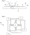
- Figure 2 shows the arrangement schematically in which liquid is supplied via inlet IN and is taken up on the other side of the element by outlet OUT which is connected to a low pressure source.
- the liquid is supplied along the direction of movement of the substrate relative to the final element, though this does not need to be the case.
- Figure 3 Various orientations and numbers of in- and out-lets positioned around the final element are possible, one example is illustrated in Figure 3 in which four sets of an inlet with an outlet on either side are provided in a regular pattern around the final element.
- a liquid supply system in a second solution may be provided that comprises a seal member which extends along at least a part of a boundary of the space between the final element of the projection system and the substrate table.
- the seal member is substantially stationary relative to the projection system in the XY plane though there may be some relative movement in the Z direction (in the direction of the optical axis).
- a seal is formed between the seal member and the surface of the substrate.
- the seal is a contactless seal such as a gas seal.
- a third solution that may be provided comprises a member attached to the projection system which forms a hollow space underneath the final element of the projection system.
- the bottom of the member is provided close enough to the surface of the substrate such that capillary forces are strong enough to contain the immersion liquid in the hollow space created by the member between the final element of the projection system and the substrate.
- each of the solutions may be improved.
- the first solution has proved to be hard to implement without large and uncontrolled liquid spillage.
- the second and third solutions may deleteriously transmit disturbance forces to the substrate and/or projection system because of their close interaction with the surface of the substrate which is necessary in order to keep the liquid in the space.
- each of the solutions may not be particularly well suited for imaging objects of different height on the substrate table, such as through lens sensors. There is not a great deal of available space with these systems between the projection system and the substrate and building a liquid supply system which can operate at high NA can be difficult.
- Each of the solutions may present difficulties with the imaging of edge portions of the substrate, such as the gas seal may become unbalanced when it is partly positioned over the edge of the substrate and/or the capillary force can be lost when imaging edge portions.
- These solutions all work best with a low free working distance (which would advantageously be higher) and with high fluid pressures (which would advantageously be lower).
- a lithographic apparatus comprising:
- the immersion liquid is allowed to leak out of the space between the bottom of the barrier member and the substrate and is thereby not constrained in the space.
- the transmission of disturbance forces between the projection system, the barrier member and the substrate may be reduced or minimized.
- a high rate of liquid replenishment in the space may be possible without the necessity for the use of high liquid pressures.
- the force in the direction of the optical axis on the substrate table may also be reduced and be more constant in comparison to other liquid supply systems.
- the imaging of edge portions may become easier as complicated measures are not necessary as the barrier member passes over the edge of the substrate as there is no seal to be disturbed at the edge of the substrate.
- the simplicity of the barrier member may be increased as only liquid inlets are required and no gas supplies. The lack of gas supplies means that the chance of bubble formation in the immersion liquid which can deleteriously affect the imaging quality may reduced or minimized.
- a larger free working distance (the distance between the projection system and the substrate) may be increased compared to other supply systems.
- the apparatus further comprises at least one outlet to remove immersion liquid, the outlet being radially outwardly of the barrier member.
- immersion liquid which has spilled from the localized area of the supply system i.e. the area under the projection system
- the outlet is on the substrate table.
- the barrier member is mechanically isolated from the projection system so that disturbance forces are not automatically transmitted to the projection system by the barrier member.
- the barrier member is connected to a base frame which supports the substrate table and/or a projection system frame which supports the projection system.
- the barrier member is free to move in the direction of an optical axis of the projection system.
- the apparatus may comprise an actuator configured to adjust the height and/or tilt of the barrier member relative to the substrate.
- a device manufacturing method comprising:
- a device manufactured according to the above-referenced device manufacturing method and/or by the above-referenced lithographic apparatus.
- lithographic apparatus in the manufacture of ICs, it should be understood that the lithographic apparatus described herein may have other applications, such as the manufacture of integrated optical systems, guidance and detection patterns for magnetic domain memories, liquid-crystal displays (LCDs), thin-film magnetic heads, etc.
- LCDs liquid-crystal displays
- any use of the terms “wafer” or “die” herein may be considered as synonymous with the more general terms “substrate” or "target portion”, respectively.
- the substrate referred to herein may be processed, before or after exposure, in for example a track (a tool that typically applies a layer of resist to a substrate and develops the exposed resist) or a metrology or inspection tool.
- the disclosure herein may be applied to such and other substrate processing tools.
- the substrate may be processed more than once, for example in order to create a multi-layer IC, so that the term substrate used herein may also refer to a substrate that already contains multiple processed layers.
- UV radiation e.g. having a wavelength of 365, 248, 193, 157 or 126 nm.
- patterning device used herein should be broadly interpreted as referring to any device that can be used to impart a projection beam with a pattern in its cross-section such as to create a pattern in a target portion of the substrate. It should be noted that the pattern imparted to the projection beam may not exactly correspond to the desired pattern in the target portion of the substrate. Generally, the pattern imparted to the projection beam will correspond to a particular functional layer in a device being created in the target portion, such as an integrated circuit.
- a patterning device may be transmissive or reflective.
- Examples of patterning devices include masks, programmable mirror arrays, and programmable LCD panels.
- Masks are well known in lithography, and include mask types such as binary, alternating phase-shift, and attenuated phase-shift, as well as various hybrid mask types.
- An example of a programmable mirror array employs a matrix arrangement of small mirrors, each of which can be individually tilted so as to reflect an incoming radiation beam in different directions; in this manner, the reflected beam is patterned.
- the support structure may be a frame or table, for example, which may be fixed or movable as required and which may ensure that the patterning device is at a desired position, for example with respect to the projection system. Any use of the terms "reticle” or “mask” herein may be considered synonymous with the more general term "patterning device”.
- projection system used herein should be broadly interpreted as encompassing various types of projection system, including refractive optical systems, reflective optical systems, and catadioptric optical systems, as appropriate for example for the exposure radiation being used, or for other factors such as the use of an immersion fluid or the use of a vacuum. Any use of the term “lens” herein may be considered as synonymous with the more general term “projection system”.
- the illumination system may also encompass various types of optical components, including refractive, reflective, and catadioptric optical components for directing, shaping, or controlling the projection beam of radiation, and such components may also be referred to below, collectively or singularly, as a "lens”.
- the lithographic apparatus may be of a type having two (dual stage) or more substrate tables (and/or two or more mask tables). In such "multiple stage” machines the additional tables may be used in parallel, or preparatory steps may be carried out on one or more tables while one or more other tables are being used for exposure.
- Figure 1 schematically depicts a lithographic apparatus according to a particular embodiment of the invention.
- the apparatus comprises:
- the apparatus is of a transmissive type (e.g. employing a transmissive mask).
- the apparatus maybe of a reflective type (e.g. employing a programmable mirror array of a type as referred to above).
- the illuminator IL receives a beam of radiation from a radiation source SO.
- the source and the lithographic apparatus may be separate entities, for example when the source is an excimer laser. In such cases, the source is not considered to form part of the lithographic apparatus and the radiation beam is passed from the source SO to the illuminator IL with the aid of a beam delivery system BD comprising for example suitable directing mirrors and/or a beam expander. In other cases the source may be integral part of the apparatus, for example when the source is a mercury lamp.
- the source SO and the illuminator IL, together with the beam delivery system BD if required, may be referred to as a radiation system.
- the illuminator IL may comprise an adjusting device AM for adjusting the angular intensity distribution of the beam.
- an adjusting device AM for adjusting the angular intensity distribution of the beam.
- the illuminator IL generally comprises various other components, such as an integrator IN and a condenser CO.
- the illuminator provides a conditioned beam of radiation, referred to as the projection beam PB, having a desired uniformity and intensity distribution in its cross-section.
- the projection beam PB is incident on the mask MA, which is held on the mask table MT. Having traversed the mask MA, the projection beam PB passes through the lens PL, which focuses the beam onto a target portion C of the substrate W.
- the substrate table WT can be moved accurately, e.g. so as to position different target portions C in the path of the beam PB.
- the first positioning device PM and another position sensor can be used to accurately position the mask MA with respect to the path of the beam PB, e.g. after mechanical retrieval from a mask library, or during a scan.
- the mask table MT may be connected to a short stroke actuator only, or may be fixed.
- Mask MA and substrate W may be aligned using mask alignment marks M1, M2 and substrate alignment marks P1, P2.
- FIG 4 shows a liquid supply system according to an embodiment of the present invention.
- the liquid supply system comprises a barrier member 10.
- the barrier member 10 surrounds the final element of the projection system PL.
- the barrier member 10 extends along at least part of the boundary of a space between the final element of the projection system PL and the substrate W.
- the space generally bounded by the projection system PL, the barrier member 10 and the substrate W is filled with an immersion liquid 5.
- the barrier member 10 is far enough above the substrate W such that capillary forces do not act to contain the immersion liquid 5 in the space between the final element of the projection system PL and the substrate W bounded by the barrier member 10; in use, such as during scanning or stepping, immersion liquid 5 flows out under the barrier member 10 as illustrated because any capillary pressure generated in the gap between the bottom of the barrier member 10 and the top of the substrate W is not large enough to contain the liquid.
- the barrier member 10 may be connected to the base frame BF, the projection system frame RF and/or another frame. In an embodiment, the barrier member 10 is mechanically isolated from the projection system PL so that disturbances forces imparted on or generated by the barrier member 10 can be prevented or at least limited from being transmitted to the projection system PL.
- the barrier member 10 may be comprised solely of the one or more inlet ports 20 so that the arrangement is similar to that shown in Figure 3 except the outlet ports OUT are inlet ports.
- the one or more inlet ports 20 are positioned circumferentially around the optical axis of the apparatus.
- Immersion liquid 5 is provided to the space through the one or more inlet ports 20 which is/are formed on a bottom inner edge of the generally annular shaped barrier member 10.
- the barrier member 10 may be other shapes whether closed (e.g., rectangular) or open (e.g., U-shaped).
- a chamber 24 provided between the one or more inlet ports 20 and the supply of immersion liquid 22, ensures that immersion liquid is provided into the space at an even pressure around the inner periphery of the barrier member 10 even though the sources of immersion liquid may be provided via one or more discrete channels 22 (as opposed to, for example, a continuous groove).
- the one or more inlet ports 20 may be a continuous groove.
- the barrier member 10 extends below the one or more inlet ports 20 radially outwardly of the one or more inlet ports 20, whereas radially inwardly the barrier member 10 is further displaced from the substrate W than on the other side of the one or more inlet ports 20. This design reduces the chance of gas inclusion at the one or more inlet ports 20.
- the bottom of the barrier member is, in an embodiment, at least 50 ⁇ m from the substrate W.
- the distance is substantially 100 ⁇ m or substantially 150 ⁇ m.
- a distance of over 300 ⁇ m (even 400 ⁇ m) may not be uncommon, for instance during scanning of sensors 70. These are typical distances if the immersion liquid is water. The required distance may be different for other liquids.
- the barrier member 10 may be moveable in the Z axis 40 such that the distance between the substrate W (or any other object) and the barrier member 10 can be adjusted.
- the barrier member may also be moveable about one or more axes substantially perpendicular to the Z axis 40 such that the tilt between the substrate W (or any other object) and the barrier member 10 can be adjusted.
- the substrate table WT may be moveable in the Z axis 40 to adjust the distance between the substrate W (or any other object) and the barrier member 10 and/or moveable about one or more axes substantially perpendicular to the Z axis 40 to adjust a tilt between the substrate W (or any other obj ect) and the barrier member 10.
- the immersion liquid is spilt radially outwardly of the barrier member 10 and flows on the substrate (or object (e.g. substrate table WT)) and immersion liquid can be provided through the one or more inlet ports 20 at a low pressure.
- the immersion liquid is water, a pressure of about 1000 Pa in the one or more inlet ports 20 is about right and with a suitable restriction between the supply channel and the containment under the projection system, a pressure of about 100 Pa can be achieved under the projection system.
- a small constant Z force on the substrate table WT is provided of about 50 mN.
- outlets 60, 63, 66 may be provided.
- the outlets are positioned radially outwardly of the barrier member 10 and do not form part of the barrier member 10. Any arrangement can be used for outlets and three possibilities are shown in Figure 4 .
- a typical outlet 60 might be one which is connected either to the base frame BF or the projection system frame RF (shown in Figure 1 ) and which removes liquid from the surface of the substrate W or substrate table WT or a substrate table mounted sensor 70 or a shutter member 80 (described in more detail hereafter).
- one or more outlets 63 may be provided in the top surface of the substrate table WT and/or one or more outlets 66 can be provided at the edge of the substrate W.
- a rim 50 may be provided around the substrate table WT.
- the liquid supply system may be used for imaging of through lens sensors 70 mounted on the substrate table WT as well as with a shutter member 80, which can be attached to the bottom of the barrier member 10 through a vacuum source, by magnets, etc. which ensures that the final element of the projection system PL is maintained wet during substrate W swap.
- Shutter members are described in more detail in U.S. patent application US 10/705,785 , herein incorporated in its entirety by reference.
- the barrier member 10 may be lowered towards the substrate W (and/or the substrate table WT may be raised towards the barrier member 10).
- Adaptive height control of the barrier member 10 could be used (see European patent application EP 03256643.2 , herein incorporated in its entirety by reference) possibly based on the position of the substrate table WT with respect to the projection system.
Landscapes
- Physics & Mathematics (AREA)
- General Physics & Mathematics (AREA)
- Health & Medical Sciences (AREA)
- Engineering & Computer Science (AREA)
- Environmental & Geological Engineering (AREA)
- Epidemiology (AREA)
- Public Health (AREA)
- Exposure And Positioning Against Photoresist Photosensitive Materials (AREA)
- Exposure Of Semiconductors, Excluding Electron Or Ion Beam Exposure (AREA)
Abstract
Description
- The present invention relates to a lithographic apparatus, a device manufacturing method and device manufactured thereby.
- A lithographic apparatus is a machine that applies a desired pattern onto a target portion of a substrate. Lithographic apparatus can be used, for example, in the manufacture of integrated circuits (ICs). In that circumstance, a patterning device, such as a mask, may be used to generate a circuit pattern corresponding to an individual layer of the IC, and this pattern can be imaged onto a target portion (e.g. comprising part of, one or several dies) on a substrate (e.g. a silicon wafer) that has a layer of radiation-sensitive material (resist). In general, a single substrate will contain a network of adjacent target portions that are successively exposed. Known lithographic apparatus include so-called steppers, in which each target portion is irradiated by exposing an entire pattern onto the target portion at one time, and so-called scanners, in which each target portion is irradiated by scanning the pattern through the projection beam in a given direction (the "scanning"-direction) while synchronously scanning the substrate parallel or anti-parallel to this direction.
- It has been proposed to immerse the substrate in the lithographic projection apparatus in a liquid having a relatively high refractive index, e.g. water, so as to fill a space between the final element of the projection system and the substrate. The point of this is to enable imaging of smaller features since the exposure radiation will have a shorter wavelength in the liquid. (The effect of the liquid may also be regarded as increasing the effective NA of the system and also increasing the depth of focus.)
- However, submersing the substrate or substrate and substrate table in a bath of liquid (see for example United States patent
US 4,509,852 , hereby incorporated in its entirety by reference) means that there is a large body of liquid that must be accelerated during a scanning exposure. This requires additional or more powerful motors and turbulence in the liquid may lead to undesirable and unpredictable effects. - One of the solutions proposed is for a liquid supply system to provide liquid on only a localized area of the substrate and in between the final element of the projection system and the substrate using a liquid supply system (the substrate generally has a larger surface area than the final element of the projection system). One way which has been proposed to arrange for this is disclosed in
PCT patent application WO 99/49504 Figures 2 and 3 , liquid is supplied by at least one inlet IN onto the substrate, preferably along the direction of movement of the substrate relative to the final element, and is removed by at least one outlet OUT after having passed under the projection system. That is, as the substrate is scanned beneath the element in a-X direction, liquid is supplied at the +X side of the element and taken up at the -X side.Figure 2 shows the arrangement schematically in which liquid is supplied via inlet IN and is taken up on the other side of the element by outlet OUT which is connected to a low pressure source. In the illustration ofFigure 2 the liquid is supplied along the direction of movement of the substrate relative to the final element, though this does not need to be the case. Various orientations and numbers of in- and out-lets positioned around the final element are possible, one example is illustrated inFigure 3 in which four sets of an inlet with an outlet on either side are provided in a regular pattern around the final element. - In addition to the solution described above, a liquid supply system in a second solution may be provided that comprises a seal member which extends along at least a part of a boundary of the space between the final element of the projection system and the substrate table. The seal member is substantially stationary relative to the projection system in the XY plane though there may be some relative movement in the Z direction (in the direction of the optical axis). A seal is formed between the seal member and the surface of the substrate. In an embodiment, the seal is a contactless seal such as a gas seal. Such a system is disclosed in U.S. patent applications
US 10/705,805 US 10/705,783 - A third solution that may be provided comprises a member attached to the projection system which forms a hollow space underneath the final element of the projection system. The bottom of the member is provided close enough to the surface of the substrate such that capillary forces are strong enough to contain the immersion liquid in the hollow space created by the member between the final element of the projection system and the substrate.
- While all of the above localized area solutions overcome the problem of needing to accelerate a large body of liquid, each of the solutions may be improved. For example, the first solution has proved to be hard to implement without large and uncontrolled liquid spillage. A further example is that the second and third solutions may deleteriously transmit disturbance forces to the substrate and/or projection system because of their close interaction with the surface of the substrate which is necessary in order to keep the liquid in the space. Furthermore, each of the solutions may not be particularly well suited for imaging objects of different height on the substrate table, such as through lens sensors. There is not a great deal of available space with these systems between the projection system and the substrate and building a liquid supply system which can operate at high NA can be difficult. Each of the solutions may present difficulties with the imaging of edge portions of the substrate, such as the gas seal may become unbalanced when it is partly positioned over the edge of the substrate and/or the capillary force can be lost when imaging edge portions. These solutions all work best with a low free working distance (which would advantageously be higher) and with high fluid pressures (which would advantageously be lower).
- Accordingly, it would be advantageous, for example, to provide immersion liquid to a space between a projection system and the substrate without some or all of the above problems, in particular avoiding significant transmission of disturbance forces to the substrate.
- According to an aspect, there is provided a lithographic apparatus comprising:
- an illumination system configured to provide a beam of radiation;
- a support structure configured to hold a patterning device, the patterning device configured to impart the beam with a pattern in its cross-section;
- a substrate table configured to hold a substrate;
- a projection system configured to project the patterned beam onto a target portion of the substrate; and
- a liquid supply system configured to provide an immersion liquid to a space between the substrate and the projection system, the liquid supply system comprising a barrier member extending along at least a part of the boundary of the space and being in a position relative to an object on the substrate table so that any capillary pressure generated by the immersion liquid between the barrier member and the object is not large enough to constrain the immersion liquid in the space,
- wherein no seal is provided between the barrier member and the object.
- In this way, in use, the immersion liquid is allowed to leak out of the space between the bottom of the barrier member and the substrate and is thereby not constrained in the space. Thus, the transmission of disturbance forces between the projection system, the barrier member and the substrate may be reduced or minimized. Furthermore, a high rate of liquid replenishment in the space may be possible without the necessity for the use of high liquid pressures. The force in the direction of the optical axis on the substrate table may also be reduced and be more constant in comparison to other liquid supply systems. Also, unlike with other supply systems, the imaging of edge portions may become easier as complicated measures are not necessary as the barrier member passes over the edge of the substrate as there is no seal to be disturbed at the edge of the substrate. The simplicity of the barrier member may be increased as only liquid inlets are required and no gas supplies. The lack of gas supplies means that the chance of bubble formation in the immersion liquid which can deleteriously affect the imaging quality may reduced or minimized. Finally, a larger free working distance (the distance between the projection system and the substrate) may be increased compared to other supply systems.
- In an embodiment, the apparatus further comprises at least one outlet to remove immersion liquid, the outlet being radially outwardly of the barrier member. In this way immersion liquid which has spilled from the localized area of the supply system (i.e. the area under the projection system) may be collected without adding to the complexity of the barrier member and without substantially transferring disturbance forces to the substrate and/or substrate table. In one embodiment the outlet is on the substrate table.
- In an embodiment, the barrier member is mechanically isolated from the projection system so that disturbance forces are not automatically transmitted to the projection system by the barrier member. In an embodiment, the barrier member is connected to a base frame which supports the substrate table and/or a projection system frame which supports the projection system. In an embodiment, the barrier member is free to move in the direction of an optical axis of the projection system.
- For flexibility of the system, the apparatus may comprise an actuator configured to adjust the height and/or tilt of the barrier member relative to the substrate.
- According to a further aspect, there is provided a device manufacturing method comprising:
- providing an immersion liquid to a space between a substrate on a substrate table and a projection system, a barrier member extending along at least a part of the boundary of the space;
- allowing immersion liquid to leak between the barrier member and an object on the substrate table by positioning at least one of the barrier member and the object so that any capillary pressure generated by the immersion liquid between the barrier member and the object is not large enough to constrain the immersion liquid in the space; and
- projecting a patterned beam of radiation onto a target portion of the substrate using the projection system.
- According to a further aspect, there is provided a device manufactured according to the above-referenced device manufacturing method and/or by the above-referenced lithographic apparatus.
- Although specific reference may be made in this text to the use of lithographic apparatus in the manufacture of ICs, it should be understood that the lithographic apparatus described herein may have other applications, such as the manufacture of integrated optical systems, guidance and detection patterns for magnetic domain memories, liquid-crystal displays (LCDs), thin-film magnetic heads, etc. The skilled artisan will appreciate that, in the context of such alternative applications, any use of the terms "wafer" or "die" herein may be considered as synonymous with the more general terms "substrate" or "target portion", respectively. The substrate referred to herein may be processed, before or after exposure, in for example a track (a tool that typically applies a layer of resist to a substrate and develops the exposed resist) or a metrology or inspection tool. Where applicable, the disclosure herein may be applied to such and other substrate processing tools. Further, the substrate may be processed more than once, for example in order to create a multi-layer IC, so that the term substrate used herein may also refer to a substrate that already contains multiple processed layers.
- The terms "radiation" and "beam" used herein encompass all types of electromagnetic radiation, including ultraviolet (UV) radiation (e.g. having a wavelength of 365, 248, 193, 157 or 126 nm).
- The term "patterning device" used herein should be broadly interpreted as referring to any device that can be used to impart a projection beam with a pattern in its cross-section such as to create a pattern in a target portion of the substrate. It should be noted that the pattern imparted to the projection beam may not exactly correspond to the desired pattern in the target portion of the substrate. Generally, the pattern imparted to the projection beam will correspond to a particular functional layer in a device being created in the target portion, such as an integrated circuit.
- A patterning device may be transmissive or reflective. Examples of patterning devices include masks, programmable mirror arrays, and programmable LCD panels. Masks are well known in lithography, and include mask types such as binary, alternating phase-shift, and attenuated phase-shift, as well as various hybrid mask types. An example of a programmable mirror array employs a matrix arrangement of small mirrors, each of which can be individually tilted so as to reflect an incoming radiation beam in different directions; in this manner, the reflected beam is patterned. In each example of a patterning device, the support structure may be a frame or table, for example, which may be fixed or movable as required and which may ensure that the patterning device is at a desired position, for example with respect to the projection system. Any use of the terms "reticle" or "mask" herein may be considered synonymous with the more general term "patterning device".
- The term "projection system" used herein should be broadly interpreted as encompassing various types of projection system, including refractive optical systems, reflective optical systems, and catadioptric optical systems, as appropriate for example for the exposure radiation being used, or for other factors such as the use of an immersion fluid or the use of a vacuum. Any use of the term "lens" herein may be considered as synonymous with the more general term "projection system".
- The illumination system may also encompass various types of optical components, including refractive, reflective, and catadioptric optical components for directing, shaping, or controlling the projection beam of radiation, and such components may also be referred to below, collectively or singularly, as a "lens".
- The lithographic apparatus may be of a type having two (dual stage) or more substrate tables (and/or two or more mask tables). In such "multiple stage" machines the additional tables may be used in parallel, or preparatory steps may be carried out on one or more tables while one or more other tables are being used for exposure.
- Embodiments of the invention will now be described, by way of example only, with reference to the accompanying schematic drawings in which corresponding reference symbols indicate corresponding parts, and in which:
-
Figure 1 depicts a lithographic apparatus according to an embodiment of the invention; -
Figure 2 illustrates, in cross-section, a liquid supply system of the prior art; -
Figure 3 illustrates, in plan, the liquid supply system ofFigure 2 ; and -
Figure 4 illustrates the liquid supply system according to an embodiment of the present invention. -
Figure 1 schematically depicts a lithographic apparatus according to a particular embodiment of the invention. The apparatus comprises: - an illumination system (illuminator) IL for providing a projection beam PB of radiation (e.g. UV radiation).
- a first support structure (e.g. a mask table) MT for supporting a patterning device (e.g. a mask) MA and connected to a first positioning device PM for accurately positioning the patterning device with respect to item PL;
- a substrate table (e.g. a wafer table) WT for holding a substrate (e.g. a resist-coated wafer) W and connected to a second positioning device PW for accurately positioning the substrate with respect to item PL; and
- a projection system (e.g. a refractive projection lens) PL for imaging a pattern imparted to the projection beam PB by patterning device MA onto a target portion C (e.g. comprising one or more dies) of the substrate W.
- As here depicted, the apparatus is of a transmissive type (e.g. employing a transmissive mask). Alternatively, the apparatus maybe of a reflective type (e.g. employing a programmable mirror array of a type as referred to above).
- The illuminator IL receives a beam of radiation from a radiation source SO. The source and the lithographic apparatus may be separate entities, for example when the source is an excimer laser. In such cases, the source is not considered to form part of the lithographic apparatus and the radiation beam is passed from the source SO to the illuminator IL with the aid of a beam delivery system BD comprising for example suitable directing mirrors and/or a beam expander. In other cases the source may be integral part of the apparatus, for example when the source is a mercury lamp. The source SO and the illuminator IL, together with the beam delivery system BD if required, may be referred to as a radiation system.
- The illuminator IL may comprise an adjusting device AM for adjusting the angular intensity distribution of the beam. Generally, at least the outer and/or inner radial extent (commonly referred to as σ-outer and σ-inner, respectively) of the intensity distribution in a pupil plane of the illuminator can be adjusted. In addition, the illuminator IL generally comprises various other components, such as an integrator IN and a condenser CO. The illuminator provides a conditioned beam of radiation, referred to as the projection beam PB, having a desired uniformity and intensity distribution in its cross-section.
- The projection beam PB is incident on the mask MA, which is held on the mask table MT. Having traversed the mask MA, the projection beam PB passes through the lens PL, which focuses the beam onto a target portion C of the substrate W. With the aid of the second positioning device PW and position sensor IF (e.g. an interferometric device), the substrate table WT can be moved accurately, e.g. so as to position different target portions C in the path of the beam PB. Similarly, the first positioning device PM and another position sensor (which is not explicitly depicted in
Figure 1 ) can be used to accurately position the mask MA with respect to the path of the beam PB, e.g. after mechanical retrieval from a mask library, or during a scan. In general, movement of the object tables MT and WT will be realized with the aid of a long-stroke module (coarse positioning) and a short-stroke module (fine positioning), which form part of the positioning devices PM and PW. However, in the case of a stepper (as opposed to a scanner) the mask table MT may be connected to a short stroke actuator only, or may be fixed. Mask MA and substrate W may be aligned using mask alignment marks M1, M2 and substrate alignment marks P1, P2. - The depicted apparatus can be used in the following preferred modes:
- 1. In step mode, the mask table MT and the substrate table WT are kept essentially stationary, while an entire pattern imparted to the projection beam is projected onto a target portion C in one go (i.e. a single static exposure). The substrate table WT is then shifted in the X and/or Y direction so that a different target portion C can be exposed. In step mode, the maximum size of the exposure field limits the size of the target portion C imaged in a single static exposure.
- 2. In scan mode, the mask table MT and the substrate table WT are scanned synchronously while a pattern imparted to the projection beam is projected onto a target portion C (i.e. a single dynamic exposure). The velocity and direction of the substrate table WT relative to the mask table MT is determined by the (de-)magnification and image reversal characteristics of the projection system PL. In scan mode, the maximum size of the exposure field limits the width (in the non-scanning direction) of the target portion in a single dynamic exposure, whereas the length of the scanning motion determines the height (in the scanning direction) of the target portion.
- 3. In another mode, the mask table MT is kept essentially stationary holding a programmable patterning device, and the substrate table WT is moved or scanned while a pattern imparted to the projection beam is projected onto a target portion C. In this mode, generally a pulsed radiation source is employed and the programmable patterning device is updated as required after each movement of the substrate table WT or in between successive radiation pulses during a scan. This mode of operation can be readily applied to maskless lithography that utilizes a programmable patterning device, such as a programmable mirror array of a type as referred to above.
- Combinations and/or variations on the above described modes of use or entirely different modes of use may also be employed.
-
Figure 4 shows a liquid supply system according to an embodiment of the present invention. The liquid supply system comprises abarrier member 10. Thebarrier member 10 surrounds the final element of the projection system PL. Thebarrier member 10 extends along at least part of the boundary of a space between the final element of the projection system PL and the substrate W. The space generally bounded by the projection system PL, thebarrier member 10 and the substrate W is filled with an immersion liquid 5. - There is no seal between the
barrier member 10 and the substrate W. Thebarrier member 10 is far enough above the substrate W such that capillary forces do not act to contain the immersion liquid 5 in the space between the final element of the projection system PL and the substrate W bounded by thebarrier member 10; in use, such as during scanning or stepping, immersion liquid 5 flows out under thebarrier member 10 as illustrated because any capillary pressure generated in the gap between the bottom of thebarrier member 10 and the top of the substrate W is not large enough to contain the liquid. Thebarrier member 10 may be connected to the base frame BF, the projection system frame RF and/or another frame. In an embodiment, thebarrier member 10 is mechanically isolated from the projection system PL so that disturbances forces imparted on or generated by thebarrier member 10 can be prevented or at least limited from being transmitted to the projection system PL. - No provision is made, for example, during scanning, to seal the space 5 to avoid loss of immersion liquid. The level of immersion liquid in the passage between the projection system PL and the
barrier member 10 is maintained as constant as possible by the provision of immersion liquid through one ormore inlet ports 20. - The
barrier member 10 may be comprised solely of the one ormore inlet ports 20 so that the arrangement is similar to that shown inFigure 3 except the outlet ports OUT are inlet ports. Thus, the one ormore inlet ports 20 are positioned circumferentially around the optical axis of the apparatus. - Immersion liquid 5 is provided to the space through the one or
more inlet ports 20 which is/are formed on a bottom inner edge of the generally annular shapedbarrier member 10. Thebarrier member 10 may be other shapes whether closed (e.g., rectangular) or open (e.g., U-shaped). Achamber 24 provided between the one ormore inlet ports 20 and the supply ofimmersion liquid 22, ensures that immersion liquid is provided into the space at an even pressure around the inner periphery of thebarrier member 10 even though the sources of immersion liquid may be provided via one or more discrete channels 22 (as opposed to, for example, a continuous groove). The one ormore inlet ports 20 may be a continuous groove. - As is illustrated in
Figure 4 , thebarrier member 10 extends below the one ormore inlet ports 20 radially outwardly of the one ormore inlet ports 20, whereas radially inwardly thebarrier member 10 is further displaced from the substrate W than on the other side of the one ormore inlet ports 20. This design reduces the chance of gas inclusion at the one ormore inlet ports 20. - In order to avoid significant capillary forces being generated by immersion liquid 5 filling the gap between the bottom of the
barrier member 10 and the top of the substrate W, the bottom of the barrier member is, in an embodiment, at least 50 µm from the substrate W. In an embodiment, the distance is substantially 100 µm or substantially 150 µm. A distance of over 300 µm (even 400 µm) may not be uncommon, for instance during scanning ofsensors 70. These are typical distances if the immersion liquid is water. The required distance may be different for other liquids. Thebarrier member 10 may be moveable in theZ axis 40 such that the distance between the substrate W (or any other object) and thebarrier member 10 can be adjusted. The barrier member may also be moveable about one or more axes substantially perpendicular to theZ axis 40 such that the tilt between the substrate W (or any other object) and thebarrier member 10 can be adjusted. Alternatively or in addition, the substrate table WT may be moveable in theZ axis 40 to adjust the distance between the substrate W (or any other object) and thebarrier member 10 and/or moveable about one or more axes substantially perpendicular to theZ axis 40 to adjust a tilt between the substrate W (or any other obj ect) and thebarrier member 10. - Therefore, in use, the immersion liquid is spilt radially outwardly of the
barrier member 10 and flows on the substrate (or object (e.g. substrate table WT)) and immersion liquid can be provided through the one ormore inlet ports 20 at a low pressure. If the immersion liquid is water, a pressure of about 1000 Pa in the one ormore inlet ports 20 is about right and with a suitable restriction between the supply channel and the containment under the projection system, a pressure of about 100 Pa can be achieved under the projection system. Thus, a small constant Z force on the substrate table WT is provided of about 50 mN. - In order to remove the immersion liquid which has been spilled from the liquid supply system, one or more of the
outlets barrier member 10 and do not form part of thebarrier member 10. Any arrangement can be used for outlets and three possibilities are shown inFigure 4 . Atypical outlet 60 might be one which is connected either to the base frame BF or the projection system frame RF (shown inFigure 1 ) and which removes liquid from the surface of the substrate W or substrate table WT or a substrate table mountedsensor 70 or a shutter member 80 (described in more detail hereafter). Alternatively or in addition, one ormore outlets 63 may be provided in the top surface of the substrate table WT and/or one ormore outlets 66 can be provided at the edge of the substrate W. In order to avoid spillage, arim 50 may be provided around the substrate table WT. - The liquid supply system may be used for imaging of through
lens sensors 70 mounted on the substrate table WT as well as with ashutter member 80, which can be attached to the bottom of thebarrier member 10 through a vacuum source, by magnets, etc. which ensures that the final element of the projection system PL is maintained wet during substrate W swap. Shutter members are described in more detail in U.S.patent application US 10/705,785 shutter member 80, thebarrier member 10 may be lowered towards the substrate W (and/or the substrate table WT may be raised towards the barrier member 10). No scanning takes place when thesensors 70 are imaged and during this time (and other times when no scanning takes place) the pressure of liquid in thebarrier member 10 can be reduced such that a meniscus can be formed between thebarrier member 10 and the substrate table WT so that less liquid escapes as well as perhaps lowering thebarrier member 10. - Adaptive height control of the
barrier member 10 could be used (see European patent applicationEP 03256643.2 - While specific embodiments of the invention have been described above, it will be appreciated that the invention may be practiced otherwise than as described. The description is not intended to limit the invention.
-
Clause 1. A lithographic apparatus comprising:- an illumination system configured to provide a beam of radiation;
- a support structure configured to hold a patterning device, the patterning device configured to impart the beam with a pattern in its cross-section;
- a substrate table configured to hold a substrate;
- a projection system configured to project the patterned beam onto a target portion of the substrate; and
- a liquid supply system configured to provide an immersion liquid to a space between the substrate and the projection system, the liquid supply system comprising a barrier member extending along at least a part of the boundary of the space and being in a position relative to an object on the substrate table so that any capillary pressure generated by the immersion liquid between the barrier member and the object is not large enough to constrain the immersion liquid in the space,
- wherein no seal is provided between the barrier member and the object.
-
Clause 2. An apparatus according toclause 1, further comprising at least one outlet to remove
immersion liquid, the at least one outlet being radially outwardly of the barrier member. - Clause 3. An apparatus according to
clause 2, wherein the at least one outlet is on the substrate table. - Clause 4. An apparatus according to
clause 2, wherein the at least one outlet is suspended above the substrate table. - Clause 5. An apparatus according to
clause 1, wherein the object comprises the substrate and a distance between the barrier member and the substrate is at least 50 µm. - Clause 6. An apparatus according to clause 4, wherein the object comprises the substrate and a distance between the barrier member and the substrate is one of substantially 100 µm, 150 µm or 300 µm.
- Clause 7. An apparatus according to
clause 1, wherein the barrier member is mechanically isolated from the projection system. - Clause 8. An apparatus according to
clause 1, wherein the barrier member is connected to at least one of a base frame that supports the substrate table and a projection system frame that supports the projection system. - Clause 9. An apparatus according to
clause 1, wherein the barrier member is free to move in the direction of an optical axis of the projection system. -
Clause 10. An apparatus according toclause 1, further comprising an actuator configured to adjust at least one of the height and tilt of the barrier member relative to the object. - Clause 11. An apparatus according to
clause 1, wherein the object comprises at least one of the substrate, a sensor and a shutter. - Clause 12. An apparatus according to
clause 1, wherein the barrier member comprises at least one inlet to supply the immersion liquid to the space. - Clause 13. A device manufacturing method comprising:
- providing an immersion liquid to a space between a substrate on a substrate table and a projection system, a barrier member extending along at least a part of the boundary of the space;
- allowing immersion liquid to leak between the barrier member and an object on the substrate table by positioning at least one of the barrier member and the object so that any capillary pressure generated by the immersion liquid between the barrier member and the object is not large enough to constrain the immersion liquid in the space; and
- projecting a patterned beam of radiation onto a target portion of the substrate using the projection system.
- Clause 14. A device manufacturing method according to clause 13, comprising removing immersion liquid through at least one outlet positioned radially outwardly of the barrier member.
- Clause 15. A device manufacturing method according to clause 14, wherein the at least one outlet is positioned on the substrate table.
- Clause 16. A device manufacturing method according to clause 13, wherein the object comprises the substrate and a distance between the barrier member and the substrate is at least 50 µm.
- Clause 17. A device manufacturing method according to clause 13, wherein the barrier member is mechanically isolated from the projection system.
- Clause 18. A device manufacturing method according to clause 13, comprising moving the barrier member in the direction of an optical axis of the projection system.
- Clause 19. A device manufacturing method according to clause 13, wherein the object comprises at least one of the substrate, a sensor and a shutter.
-
Clause 20. A device manufacturing method according to clause 13, comprising supplying the immersion liquid, from the barrier member, to the space. - Clause 21. A lithographic apparatus comprising:
- an illumination system configured to provide a beam of radiation;
- a support structure configured to hold a patterning device, the patterning device configured to impart the beam with a pattern in its cross-section;
- a substrate table configured to hold a substrate;
- a projection system configured to project the patterned beam onto a target portion of the substrate; and
- a liquid supply system configured to provide an immersion liquid to a space between the substrate and the projection system, the liquid supply system comprising at least one immersion liquid inlet port provided on a boundary of the space,
wherein the immersion liquid is not substantially confined in the space so that immersion liquid can flow out of the space.
-
Clause 22. An apparatus according to clause 21, further comprising at least one immersion liquid outlet port, the at least one immersion liquid outlet port being radially outwardly of the at least one immersion liquid inlet port. - Clause 23. An apparatus according to
clause 22, wherein the at least one immersion liquid outlet is on the substrate table. -
Clause 24. An apparatus according toclause 22, wherein the outlet is suspended above the substrate table. - Clause 25. An apparatus according to clause 21, wherein a distance between the barrier member and the substrate is at least 50 µm.
- Clause 26. An apparatus according to clause 21, wherein the at least one immersion liquid inlet port is mechanically isolated from the projection system.
- Clause 27. An apparatus according to clause 21, wherein the least one immersion liquid inlet port is connected to at least one of a base frame that supports the substrate table and a projection system frame that supports the projection system.
- Clause 28. An apparatus according to clause 21, wherein the at least one immersion liquid inlet port is free to move in the direction of an optical axis of the projection system.
- Clause 29. An apparatus according to clause 21, further comprising an actuator configured to adjust at least one of the height and tilt of the least one immersion liquid inlet port relative to the substrate.
-
Clause 30. A lithographic apparatus comprising:- an illumination system configured to provide a beam of radiation;
- a support structure configured to hold a patterning device, the patterning device configured to impart the beam with a pattern in its cross-section;
- a substrate table configured to hold a substrate;
- a projection system configured to project the patterned beam onto a target portion of the substrate; and
- a liquid supply system configured to provide an immersion liquid to a space between the substrate and the projection system, the liquid supply system comprising at least one immersion liquid inlet port,
- wherein an at least one immersion liquid outlet port is provided only at least one of on the substrate table and suspended above the substrate table.
- Clause 31. An apparatus according to
clause 30, wherein the at least one immersion liquid outlet port is radially outwardly of the at least one immersion liquid inlet port. - Clause 32. An apparatus according to
clause 30, wherein a distance between the at least one immersion liquid inlet port and the substrate is at least 50 µm. - Clause 33. An apparatus according to
clause 30, wherein the at least one immersion liquid inlet port is mechanically isolated from the projection system. - Clause 34. An apparatus according to
clause 30, wherein the at least one immersion liquid inlet port is connected to at least one of a base frame that supports the substrate table and a projection system frame that supports the projection system.
Claims (8)
- A lithographic apparatus, comprising:a projection system (PL) configured to project a patterned beam onto a target portion of a substrate (W);a barrier member (10) surrounding the projection system (PL) and comprising a liquid inlet port (20) configured to supply immersion liquid (5) to a space between the substrate (W) and the projection system (PL); anda substrate table (WT) configured to hold the substrate (W), the substrate table (WT) movable relative to the liquid inlet port (20) and the substrate table (WT) comprising:a first outlet (66) at the edge of the substrate (W), the first outlet (66) configured to remove at least part of the immersion liquid (5);a sensor (70) located at a top side of the substrate table (WT) and located horizontally outward of the first outlet (66); anda second outlet (63), located horizontally outward of the first outlet (63) and configured to remove at least part of the immersion liquid (5).
- The lithographic apparatus of claim 1, wherein the second outlet (63) is located in the top surface of the substrate table (WT) to remove the immersion liquid (5), and the second outlet (63) is arranged to be essentially co-planar with the sensor (70).
- The lithographic apparatus of claim 1 or 2, further comprising an actuator configured to adjust a height, or a tilt, or both, of at least part of the barrier member (10) relative to the substrate (W).
- The lithographic apparatus of claim 1, 2 or 3, wherein the liquid inlet port (20) is located on an inner periphery of the barrier member (10) and the liquid inlet port (20) is located below a bottom surface of the projection system (PL).
- The lithographic apparatus of any of the preceding claims, further comprising a third outlet (60) located above the substrate table (WT), the third outlet (60) outward of, and separated from, an outer periphery of the barrier member (10) and configured to remove at least part of the immersion liquid (5).
- The lithographic apparatus of any of the preceding claims, wherein an upper surface of the substrate (W) when held by the substrate table (WT) and an upper surface of the sensor (70) are essentially co-planar.
- The lithographic apparatus of any of the preceding claims, wherein the barrier member (10) is mechanically isolated from the projection system (PL).
- The lithographic apparatus of any of the preceding claims, further comprising a rim (50) around the substrate table (WT).
Applications Claiming Priority (4)
| Application Number | Priority Date | Filing Date | Title |
|---|---|---|---|
| US10/743,271 US7394521B2 (en) | 2003-12-23 | 2003-12-23 | Lithographic apparatus and device manufacturing method |
| EP10180289.0A EP2259139B1 (en) | 2003-12-23 | 2004-12-15 | Lithographic apparatus and device manufacturing method |
| PCT/EP2004/014282 WO2005064405A2 (en) | 2003-12-23 | 2004-12-15 | Lithographic apparatus and device manufacturing method |
| EP04803901A EP1697799A2 (en) | 2003-12-23 | 2004-12-15 | Lithographic apparatus and device manufacturing method |
Related Parent Applications (4)
| Application Number | Title | Priority Date | Filing Date |
|---|---|---|---|
| EP04803901A Division EP1697799A2 (en) | 2003-12-23 | 2004-12-15 | Lithographic apparatus and device manufacturing method |
| EP10180289.0A Division EP2259139B1 (en) | 2003-12-23 | 2004-12-15 | Lithographic apparatus and device manufacturing method |
| EP10180289.0A Previously-Filed-Application EP2259139B1 (en) | 2003-12-23 | 2004-12-15 | Lithographic apparatus and device manufacturing method |
| EP10180289.0A Division-Into EP2259139B1 (en) | 2003-12-23 | 2004-12-15 | Lithographic apparatus and device manufacturing method |
Publications (2)
| Publication Number | Publication Date |
|---|---|
| EP3287848A1 true EP3287848A1 (en) | 2018-02-28 |
| EP3287848B1 EP3287848B1 (en) | 2018-11-07 |
Family
ID=34678626
Family Applications (3)
| Application Number | Title | Priority Date | Filing Date |
|---|---|---|---|
| EP10180289.0A Expired - Lifetime EP2259139B1 (en) | 2003-12-23 | 2004-12-15 | Lithographic apparatus and device manufacturing method |
| EP04803901A Withdrawn EP1697799A2 (en) | 2003-12-23 | 2004-12-15 | Lithographic apparatus and device manufacturing method |
| EP17181223.3A Expired - Lifetime EP3287848B1 (en) | 2003-12-23 | 2004-12-15 | Lithographic apparatus |
Family Applications Before (2)
| Application Number | Title | Priority Date | Filing Date |
|---|---|---|---|
| EP10180289.0A Expired - Lifetime EP2259139B1 (en) | 2003-12-23 | 2004-12-15 | Lithographic apparatus and device manufacturing method |
| EP04803901A Withdrawn EP1697799A2 (en) | 2003-12-23 | 2004-12-15 | Lithographic apparatus and device manufacturing method |
Country Status (7)
| Country | Link |
|---|---|
| US (2) | US7394521B2 (en) |
| EP (3) | EP2259139B1 (en) |
| JP (2) | JP4157146B2 (en) |
| KR (1) | KR100855337B1 (en) |
| CN (2) | CN100507721C (en) |
| TW (1) | TWI261151B (en) |
| WO (1) | WO2005064405A2 (en) |
Families Citing this family (218)
| Publication number | Priority date | Publication date | Assignee | Title |
|---|---|---|---|---|
| US10503084B2 (en) | 2002-11-12 | 2019-12-10 | Asml Netherlands B.V. | Lithographic apparatus and device manufacturing method |
| DE60335595D1 (en) * | 2002-11-12 | 2011-02-17 | Asml Netherlands Bv | Immersion lithographic apparatus and method of making a device |
| TWI251127B (en) | 2002-11-12 | 2006-03-11 | Asml Netherlands Bv | Lithographic apparatus and device manufacturing method |
| US7372541B2 (en) | 2002-11-12 | 2008-05-13 | Asml Netherlands B.V. | Lithographic apparatus and device manufacturing method |
| US9482966B2 (en) | 2002-11-12 | 2016-11-01 | Asml Netherlands B.V. | Lithographic apparatus and device manufacturing method |
| US7110081B2 (en) | 2002-11-12 | 2006-09-19 | Asml Netherlands B.V. | Lithographic apparatus and device manufacturing method |
| SG2010050110A (en) * | 2002-11-12 | 2014-06-27 | Asml Netherlands Bv | Lithographic apparatus and device manufacturing method |
| SG121822A1 (en) | 2002-11-12 | 2006-05-26 | Asml Netherlands Bv | Lithographic apparatus and device manufacturing method |
| CN1723541B (en) * | 2002-12-10 | 2010-06-02 | 株式会社尼康 | Exposure apparatus and device manufacturing method |
| US7242455B2 (en) * | 2002-12-10 | 2007-07-10 | Nikon Corporation | Exposure apparatus and method for producing device |
| DE10261775A1 (en) | 2002-12-20 | 2004-07-01 | Carl Zeiss Smt Ag | Device for the optical measurement of an imaging system |
| KR101506408B1 (en) * | 2003-02-26 | 2015-03-26 | 가부시키가이샤 니콘 | Exposure apparatus and method, and method of producing apparatus |
| EP1610361B1 (en) | 2003-03-25 | 2014-05-21 | Nikon Corporation | Exposure system and device production method |
| KR101176817B1 (en) * | 2003-04-07 | 2012-08-24 | 가부시키가이샤 니콘 | Exposure apparatus and method for manufacturing device |
| WO2004093159A2 (en) | 2003-04-09 | 2004-10-28 | Nikon Corporation | Immersion lithography fluid control system |
| KR20180089562A (en) * | 2003-04-10 | 2018-08-08 | 가부시키가이샤 니콘 | Environmental system including vaccum scavange for an immersion lithography apparatus |
| EP3062152B1 (en) * | 2003-04-10 | 2017-12-20 | Nikon Corporation | Environmental system including vaccum scavenge for an immersion lithography apparatus |
| JP4656057B2 (en) * | 2003-04-10 | 2011-03-23 | 株式会社ニコン | Electro-osmotic element for immersion lithography equipment |
| WO2004093160A2 (en) | 2003-04-10 | 2004-10-28 | Nikon Corporation | Run-off path to collect liquid for an immersion lithography apparatus |
| JP4582089B2 (en) | 2003-04-11 | 2010-11-17 | 株式会社ニコン | Liquid jet recovery system for immersion lithography |
| JP4315198B2 (en) | 2003-04-11 | 2009-08-19 | 株式会社ニコン | Lithographic apparatus for maintaining immersion liquid under an optical assembly, immersion liquid maintenance method and device manufacturing method using them |
| KR101324818B1 (en) | 2003-04-11 | 2013-11-01 | 가부시키가이샤 니콘 | Cleanup method for optics in immersion lithography |
| CN1774667A (en) | 2003-04-17 | 2006-05-17 | 株式会社尼康 | Optical arrangement of autofocus elements for use with immersion lithography |
| TWI295414B (en) | 2003-05-13 | 2008-04-01 | Asml Netherlands Bv | Lithographic apparatus and device manufacturing method |
| WO2004102646A1 (en) * | 2003-05-15 | 2004-11-25 | Nikon Corporation | Exposure apparatus and method for manufacturing device |
| TWI511181B (en) * | 2003-05-23 | 2015-12-01 | 尼康股份有限公司 | Exposure method and exposure apparatus, and device manufacturing method |
| TWI518742B (en) * | 2003-05-23 | 2016-01-21 | 尼康股份有限公司 | A method of manufacturing an exposure apparatus and an element |
| KR20180122033A (en) * | 2003-05-28 | 2018-11-09 | 가부시키가이샤 니콘 | Exposure method, exposure device, and device manufacturing method |
| TWI347741B (en) * | 2003-05-30 | 2011-08-21 | Asml Netherlands Bv | Lithographic apparatus and device manufacturing method |
| US7213963B2 (en) | 2003-06-09 | 2007-05-08 | Asml Netherlands B.V. | Lithographic apparatus and device manufacturing method |
| EP2261742A3 (en) | 2003-06-11 | 2011-05-25 | ASML Netherlands BV | Lithographic apparatus and device manufacturing method. |
| TWI409853B (en) | 2003-06-13 | 2013-09-21 | 尼康股份有限公司 | An exposure method, a substrate stage, an exposure apparatus, and an element manufacturing method |
| DE602004024782D1 (en) * | 2003-06-19 | 2010-02-04 | Nippon Kogaku Kk | EXPOSURE DEVICE AND COMPONENT MANUFACTURING METHOD |
| WO2005006026A2 (en) * | 2003-07-01 | 2005-01-20 | Nikon Corporation | Using isotopically specified fluids as optical elements |
| EP3179309A1 (en) | 2003-07-08 | 2017-06-14 | Nikon Corporation | Wafer table for immersion lithography |
| WO2005006415A1 (en) | 2003-07-09 | 2005-01-20 | Nikon Corporation | Exposure apparatus and method for manufacturing device |
| WO2005006418A1 (en) * | 2003-07-09 | 2005-01-20 | Nikon Corporation | Exposure apparatus and method for manufacturing device |
| DE602004030247D1 (en) * | 2003-07-09 | 2011-01-05 | Nippon Kogaku Kk | EXPOSURE DEVICE AND METHOD FOR MANUFACTURING THE CONSTRUCTION |
| SG109000A1 (en) | 2003-07-16 | 2005-02-28 | Asml Netherlands Bv | Lithographic apparatus and device manufacturing method |
| EP1500982A1 (en) | 2003-07-24 | 2005-01-26 | ASML Netherlands B.V. | Lithographic apparatus and device manufacturing method |
| EP1650787A4 (en) * | 2003-07-25 | 2007-09-19 | Nikon Corp | Inspection method and inspection device for projection optical system, and production method for projection optical system |
| EP1503244A1 (en) | 2003-07-28 | 2005-02-02 | ASML Netherlands B.V. | Lithographic projection apparatus and device manufacturing method |
| KR101641011B1 (en) * | 2003-07-28 | 2016-07-19 | 가부시키가이샤 니콘 | Exposure apparatus, device producing method, and exposure apparatus controlling method |
| US7779781B2 (en) | 2003-07-31 | 2010-08-24 | Asml Netherlands B.V. | Lithographic apparatus and device manufacturing method |
| EP1670038B1 (en) * | 2003-08-26 | 2012-06-06 | Nikon Corporation | Optical element and exposure apparatus |
| US8149381B2 (en) * | 2003-08-26 | 2012-04-03 | Nikon Corporation | Optical element and exposure apparatus |
| EP2261740B1 (en) | 2003-08-29 | 2014-07-09 | ASML Netherlands BV | Lithographic apparatus |
| TWI245163B (en) | 2003-08-29 | 2005-12-11 | Asml Netherlands Bv | Lithographic apparatus and device manufacturing method |
| TWI263859B (en) | 2003-08-29 | 2006-10-11 | Asml Netherlands Bv | Lithographic apparatus and device manufacturing method |
| KR101419192B1 (en) * | 2003-08-29 | 2014-07-15 | 가부시키가이샤 니콘 | Exposure apparatus and device producing method |
| KR101288140B1 (en) * | 2003-09-03 | 2013-07-19 | 가부시키가이샤 니콘 | Apparatus and method for providing fluid for immersion lithography |
| WO2005029559A1 (en) * | 2003-09-19 | 2005-03-31 | Nikon Corporation | Exposure apparatus and device producing method |
| KR101743378B1 (en) * | 2003-09-29 | 2017-06-15 | 가부시키가이샤 니콘 | Exposure apparatus, exposure method, and device manufacturing method |
| JP2005136364A (en) * | 2003-10-08 | 2005-05-26 | Zao Nikon Co Ltd | Substrate transport apparatus, exposure apparatus, and device manufacturing method |
| KR101111364B1 (en) | 2003-10-08 | 2012-02-27 | 가부시키가이샤 자오 니콘 | Substrate carrying apparatus, substrate carrying method, exposure apparatus, exposure method, and method for producing device |
| WO2005036623A1 (en) | 2003-10-08 | 2005-04-21 | Zao Nikon Co., Ltd. | Substrate transporting apparatus and method, exposure apparatus and method, and device producing method |
| TWI553701B (en) | 2003-10-09 | 2016-10-11 | 尼康股份有限公司 | Exposure apparatus and exposure method, component manufacturing method |
| EP1524557A1 (en) * | 2003-10-15 | 2005-04-20 | ASML Netherlands B.V. | Lithographic apparatus and device manufacturing method |
| EP1524558A1 (en) | 2003-10-15 | 2005-04-20 | ASML Netherlands B.V. | Lithographic apparatus and device manufacturing method |
| US7411653B2 (en) * | 2003-10-28 | 2008-08-12 | Asml Netherlands B.V. | Lithographic apparatus |
| JP4513747B2 (en) | 2003-10-31 | 2010-07-28 | 株式会社ニコン | Exposure apparatus and device manufacturing method |
| JP4295712B2 (en) | 2003-11-14 | 2009-07-15 | エーエスエムエル ネザーランズ ビー.ブイ. | Lithographic apparatus and apparatus manufacturing method |
| US7545481B2 (en) | 2003-11-24 | 2009-06-09 | Asml Netherlands B.V. | Lithographic apparatus and device manufacturing method |
| TWI605315B (en) | 2003-12-03 | 2017-11-11 | 尼康股份有限公司 | Exposure device, exposure method, and device manufacturing method |
| US20070081133A1 (en) * | 2004-12-14 | 2007-04-12 | Niikon Corporation | Projection exposure apparatus and stage unit, and exposure method |
| KR101111363B1 (en) * | 2003-12-15 | 2012-04-12 | 가부시키가이샤 니콘 | Projection exposure apparatus, stage apparatus, and exposure method |
| KR101941351B1 (en) | 2003-12-15 | 2019-01-22 | 가부시키가이샤 니콘 | Stage system, exposure apparatus and exposure method |
| US7589818B2 (en) * | 2003-12-23 | 2009-09-15 | Asml Netherlands B.V. | Lithographic apparatus, alignment apparatus, device manufacturing method, and a method of converting an apparatus |
| US7394521B2 (en) * | 2003-12-23 | 2008-07-01 | Asml Netherlands B.V. | Lithographic apparatus and device manufacturing method |
| JP2005191394A (en) * | 2003-12-26 | 2005-07-14 | Canon Inc | Exposure method and apparatus |
| WO2005071491A2 (en) * | 2004-01-20 | 2005-08-04 | Carl Zeiss Smt Ag | Exposure apparatus and measuring device for a projection lens |
| US7589822B2 (en) | 2004-02-02 | 2009-09-15 | Nikon Corporation | Stage drive method and stage unit, exposure apparatus, and device manufacturing method |
| KR101276392B1 (en) | 2004-02-03 | 2013-06-19 | 가부시키가이샤 니콘 | Exposure apparatus and method of producing device |
| US7050146B2 (en) | 2004-02-09 | 2006-05-23 | Asml Netherlands B.V. | Lithographic apparatus and device manufacturing method |
| KR101504445B1 (en) | 2004-03-25 | 2015-03-19 | 가부시키가이샤 니콘 | Exposure apparatus and method for manufacturing device |
| US7034917B2 (en) * | 2004-04-01 | 2006-04-25 | Asml Netherlands B.V. | Lithographic apparatus, device manufacturing method and device manufactured thereby |
| US7898642B2 (en) | 2004-04-14 | 2011-03-01 | Asml Netherlands B.V. | Lithographic apparatus and device manufacturing method |
| US7379159B2 (en) | 2004-05-03 | 2008-05-27 | Asml Netherlands B.V. | Lithographic apparatus and device manufacturing method |
| US8054448B2 (en) * | 2004-05-04 | 2011-11-08 | Nikon Corporation | Apparatus and method for providing fluid for immersion lithography |
| US7616383B2 (en) * | 2004-05-18 | 2009-11-10 | Asml Netherlands B.V. | Lithographic apparatus and device manufacturing method |
| US7486381B2 (en) * | 2004-05-21 | 2009-02-03 | Asml Netherlands B.V. | Lithographic apparatus and device manufacturing method |
| US7796274B2 (en) | 2004-06-04 | 2010-09-14 | Carl Zeiss Smt Ag | System for measuring the image quality of an optical imaging system |
| KR101162128B1 (en) * | 2004-06-09 | 2012-07-03 | 가부시키가이샤 니콘 | Exposure system and device production method |
| US7481867B2 (en) | 2004-06-16 | 2009-01-27 | Edwards Limited | Vacuum system for immersion photolithography |
| US8698998B2 (en) | 2004-06-21 | 2014-04-15 | Nikon Corporation | Exposure apparatus, method for cleaning member thereof, maintenance method for exposure apparatus, maintenance device, and method for producing device |
| EP3462241A1 (en) * | 2004-06-21 | 2019-04-03 | Nikon Corporation | Exposure apparatus, exposure method and method for producing a device |
| US7463330B2 (en) | 2004-07-07 | 2008-12-09 | Asml Netherlands B.V. | Lithographic apparatus and device manufacturing method |
| US8384874B2 (en) * | 2004-07-12 | 2013-02-26 | Nikon Corporation | Immersion exposure apparatus and device manufacturing method to detect if liquid on base member |
| US7304715B2 (en) | 2004-08-13 | 2007-12-04 | Asml Netherlands B.V. | Lithographic apparatus and device manufacturing method |
| US8305553B2 (en) * | 2004-08-18 | 2012-11-06 | Nikon Corporation | Exposure apparatus and device manufacturing method |
| US7701550B2 (en) * | 2004-08-19 | 2010-04-20 | Asml Netherlands B.V. | Lithographic apparatus and device manufacturing method |
| TWI610340B (en) * | 2004-09-17 | 2018-01-01 | 尼康股份有限公司 | Exposure apparatus, exposure method, and component manufacturing method |
| US7522261B2 (en) * | 2004-09-24 | 2009-04-21 | Asml Netherlands B.V. | Lithographic apparatus and device manufacturing method |
| US7355674B2 (en) * | 2004-09-28 | 2008-04-08 | Asml Netherlands B.V. | Lithographic apparatus, device manufacturing method and computer program product |
| US7894040B2 (en) * | 2004-10-05 | 2011-02-22 | Asml Netherlands B.V. | Lithographic apparatus and device manufacturing method |
| US7379155B2 (en) | 2004-10-18 | 2008-05-27 | Asml Netherlands B.V. | Lithographic apparatus and device manufacturing method |
| US7414699B2 (en) * | 2004-11-12 | 2008-08-19 | Asml Netherlands B.V. | Lithographic apparatus and device manufacturing method |
| US7583357B2 (en) * | 2004-11-12 | 2009-09-01 | Asml Netherlands B.V. | Lithographic apparatus and device manufacturing method |
| US7423720B2 (en) | 2004-11-12 | 2008-09-09 | Asml Netherlands B.V. | Lithographic apparatus and device manufacturing method |
| US7161654B2 (en) * | 2004-12-02 | 2007-01-09 | Asml Netherlands B.V. | Lithographic apparatus and device manufacturing method |
| US7397533B2 (en) * | 2004-12-07 | 2008-07-08 | Asml Netherlands B.V. | Lithographic apparatus and device manufacturing method |
| US7365827B2 (en) | 2004-12-08 | 2008-04-29 | Asml Netherlands B.V. | Lithographic apparatus and device manufacturing method |
| US7403261B2 (en) * | 2004-12-15 | 2008-07-22 | Asml Netherlands B.V. | Lithographic apparatus and device manufacturing method |
| US7880860B2 (en) * | 2004-12-20 | 2011-02-01 | Asml Netherlands B.V. | Lithographic apparatus and device manufacturing method |
| US7450217B2 (en) | 2005-01-12 | 2008-11-11 | Asml Netherlands B.V. | Exposure apparatus, coatings for exposure apparatus, lithographic apparatus, device manufacturing method, and device manufactured thereby |
| DE602006012746D1 (en) | 2005-01-14 | 2010-04-22 | Asml Netherlands Bv | Lithographic apparatus and manufacturing method |
| US8692973B2 (en) * | 2005-01-31 | 2014-04-08 | Nikon Corporation | Exposure apparatus and method for producing device |
| EP3079164A1 (en) * | 2005-01-31 | 2016-10-12 | Nikon Corporation | Exposure apparatus and method for producing device |
| US7282701B2 (en) | 2005-02-28 | 2007-10-16 | Asml Netherlands B.V. | Sensor for use in a lithographic apparatus |
| US7684010B2 (en) * | 2005-03-09 | 2010-03-23 | Asml Netherlands B.V. | Lithographic apparatus, device manufacturing method, seal structure, method of removing an object and a method of sealing |
| US7411654B2 (en) * | 2005-04-05 | 2008-08-12 | Asml Netherlands B.V. | Lithographic apparatus and device manufacturing method |
| USRE43576E1 (en) | 2005-04-08 | 2012-08-14 | Asml Netherlands B.V. | Dual stage lithographic apparatus and device manufacturing method |
| US7468779B2 (en) * | 2005-06-28 | 2008-12-23 | Asml Netherlands B.V. | Lithographic apparatus and device manufacturing method |
| US7535644B2 (en) * | 2005-08-12 | 2009-05-19 | Asml Netherlands B.V. | Lens element, lithographic apparatus, device manufacturing method, and device manufactured thereby |
| US7357768B2 (en) * | 2005-09-22 | 2008-04-15 | William Marshall | Recliner exerciser |
| US20070124987A1 (en) * | 2005-12-05 | 2007-06-07 | Brown Jeffrey K | Electronic pest control apparatus |
| KR100768849B1 (en) * | 2005-12-06 | 2007-10-22 | 엘지전자 주식회사 | Power supply system and method for grid-connected fuel cell system |
| US7649611B2 (en) | 2005-12-30 | 2010-01-19 | Asml Netherlands B.V. | Lithographic apparatus and device manufacturing method |
| US7446859B2 (en) * | 2006-01-27 | 2008-11-04 | International Business Machines Corporation | Apparatus and method for reducing contamination in immersion lithography |
| JP4889331B2 (en) * | 2006-03-22 | 2012-03-07 | 大日本スクリーン製造株式会社 | Substrate processing apparatus and substrate processing method |
| EP2005222A4 (en) * | 2006-04-03 | 2010-07-28 | Incidence surfaces and optical windows that are solvophobic to immersion liquids | |
| US9477158B2 (en) * | 2006-04-14 | 2016-10-25 | Asml Netherlands B.V. | Lithographic apparatus and device manufacturing method |
| DE102006021797A1 (en) | 2006-05-09 | 2007-11-15 | Carl Zeiss Smt Ag | Optical imaging device with thermal damping |
| US7656502B2 (en) | 2006-06-22 | 2010-02-02 | Asml Netherlands B.V. | Lithographic apparatus and device manufacturing method |
| US7843548B2 (en) * | 2006-11-13 | 2010-11-30 | Asml Netherlands B.V. | Conduit system for a lithographic apparatus, lithographic apparatus, pump, and method for substantially reducing vibrations in a conduit system |
| SG143137A1 (en) | 2006-11-13 | 2008-06-27 | Asml Netherlands Bv | Conduit system for a lithographic apparatus, lithographic apparatus, pump, and method for substantially reducing vibrations in a conduit system |
| US9632425B2 (en) | 2006-12-07 | 2017-04-25 | Asml Holding N.V. | Lithographic apparatus, a dryer and a method of removing liquid from a surface |
| KR100843709B1 (en) * | 2007-02-05 | 2008-07-04 | 삼성전자주식회사 | Liquid sealing unit and emulsion photolithography apparatus having same |
| US8654305B2 (en) * | 2007-02-15 | 2014-02-18 | Asml Holding N.V. | Systems and methods for insitu lens cleaning in immersion lithography |
| US8817226B2 (en) | 2007-02-15 | 2014-08-26 | Asml Holding N.V. | Systems and methods for insitu lens cleaning using ozone in immersion lithography |
| US7692765B2 (en) | 2007-02-21 | 2010-04-06 | Asml Netherlands B.V. | Lithographic apparatus and method of removing liquid |
| CN100462848C (en) * | 2007-03-15 | 2009-02-18 | 浙江大学 | Sealed control device for liquid supply and recovery in immersion lithography system |
| US8237911B2 (en) | 2007-03-15 | 2012-08-07 | Nikon Corporation | Apparatus and methods for keeping immersion fluid adjacent to an optical assembly during wafer exchange in an immersion lithography machine |
| NL1036186A1 (en) * | 2007-12-03 | 2009-06-04 | Asml Netherlands Bv | Lithographic apparatus and device manufacturing method. |
| NL1036579A1 (en) * | 2008-02-19 | 2009-08-20 | Asml Netherlands Bv | Lithographic apparatus and methods. |
| NL1036631A1 (en) | 2008-03-24 | 2009-09-25 | Asml Netherlands Bv | Immersion Lithographic Apparatus and Device Manufacturing Method. |
| KR101448152B1 (en) * | 2008-03-26 | 2014-10-07 | 삼성전자주식회사 | Distance measuring sensor having vertical photogate and three dimensional color image sensor having the same |
| NL1036715A1 (en) | 2008-04-16 | 2009-10-19 | Asml Netherlands Bv | Lithographic apparatus. |
| NL1036709A1 (en) | 2008-04-24 | 2009-10-27 | Asml Netherlands Bv | Lithographic apparatus and a method of operating the apparatus. |
| EP2131241B1 (en) | 2008-05-08 | 2019-07-31 | ASML Netherlands B.V. | Fluid handling structure, lithographic apparatus and device manufacturing method |
| US8421993B2 (en) | 2008-05-08 | 2013-04-16 | Asml Netherlands B.V. | Fluid handling structure, lithographic apparatus and device manufacturing method |
| EP2249205B1 (en) | 2008-05-08 | 2012-03-07 | ASML Netherlands BV | Immersion lithographic apparatus, drying device, immersion metrology apparatus and device manufacturing method |
| NL1036835A1 (en) | 2008-05-08 | 2009-11-11 | Asml Netherlands Bv | Lithographic Apparatus and Method. |
| US9176393B2 (en) | 2008-05-28 | 2015-11-03 | Asml Netherlands B.V. | Lithographic apparatus and a method of operating the apparatus |
| NL1036924A1 (en) | 2008-06-02 | 2009-12-03 | Asml Netherlands Bv | Substrate table, lithographic apparatus and device manufacturing method. |
| EP2131242A1 (en) * | 2008-06-02 | 2009-12-09 | ASML Netherlands B.V. | Substrate table, lithographic apparatus and device manufacturing method |
| NL2002964A1 (en) | 2008-06-16 | 2009-12-17 | Asml Netherlands Bv | Lithographic Apparatus, a Metrology Apparatus and a Method of Using the Apparatus. |
| EP2136250A1 (en) | 2008-06-18 | 2009-12-23 | ASML Netherlands B.V. | Lithographic apparatus and method |
| NL2002983A1 (en) | 2008-06-26 | 2009-12-29 | Asml Netherlands Bv | A lithographic apparatus and a method of operating the lithographic apparatus. |
| NL2003111A1 (en) | 2008-07-25 | 2010-01-26 | Asml Netherlands Bv | Method of designing sets or mask patterns, sets of mask patterns, and device manufacturing method. |
| NL2003225A1 (en) | 2008-07-25 | 2010-01-26 | Asml Netherlands Bv | Fluid handling structure, lithographic apparatus and device manufacturing method. |
| NL2003226A (en) | 2008-08-19 | 2010-03-09 | Asml Netherlands Bv | Lithographic apparatus, drying device, metrology apparatus and device manufacturing method. |
| SG159467A1 (en) | 2008-09-02 | 2010-03-30 | Asml Netherlands Bv | Fluid handling structure, lithographic apparatus and device manufacturing method |
| NL2003363A (en) | 2008-09-10 | 2010-03-15 | Asml Netherlands Bv | Lithographic apparatus, method of manufacturing an article for a lithographic apparatus and device manufacturing method. |
| NL2003392A (en) | 2008-09-17 | 2010-03-18 | Asml Netherlands Bv | Lithographic apparatus and a method of operating the apparatus. |
| NL2003362A (en) | 2008-10-16 | 2010-04-19 | Asml Netherlands Bv | Lithographic apparatus and device manufacturing method. |
| NL2003333A (en) | 2008-10-23 | 2010-04-26 | Asml Netherlands Bv | Fluid handling structure, lithographic apparatus and device manufacturing method. |
| NL2003575A (en) | 2008-10-29 | 2010-05-03 | Asml Netherlands Bv | Lithographic apparatus and device manufacturing method. |
| NL2003638A (en) | 2008-12-03 | 2010-06-07 | Asml Netherlands Bv | Lithographic apparatus and device manufacturing method. |
| NL2003758A (en) | 2008-12-04 | 2010-06-07 | Asml Netherlands Bv | A member with a cleaning surface and a method of removing contamination. |
| JP5199982B2 (en) | 2008-12-08 | 2013-05-15 | エーエスエムエル ネザーランズ ビー.ブイ. | Lithographic apparatus |
| EP2196857A3 (en) | 2008-12-09 | 2010-07-21 | ASML Netherlands BV | Lithographic apparatus and device manufacturing method |
| JP5001343B2 (en) | 2008-12-11 | 2012-08-15 | エーエスエムエル ネザーランズ ビー.ブイ. | Fluid extraction system, immersion lithographic apparatus, and method for reducing pressure fluctuations of an immersion liquid used in an immersion lithographic apparatus |
| JP2010147471A (en) | 2008-12-18 | 2010-07-01 | Asml Netherlands Bv | Lithographic apparatus, and method of irradiating at least two target portions |
| EP2221669A3 (en) | 2009-02-19 | 2011-02-09 | ASML Netherlands B.V. | A lithographic apparatus, a method of controlling the apparatus and a device manufacturing method |
| NL2004305A (en) | 2009-03-13 | 2010-09-14 | Asml Netherlands Bv | Substrate table, immersion lithographic apparatus and device manufacturing method. |
| JP2010251745A (en) | 2009-04-10 | 2010-11-04 | Asml Netherlands Bv | Immersion lithography device and device manufacturing method |
| NL2004362A (en) | 2009-04-10 | 2010-10-12 | Asml Netherlands Bv | A fluid handling device, an immersion lithographic apparatus and a device manufacturing method. |
| NL2004497A (en) | 2009-05-01 | 2010-11-02 | Asml Netherlands Bv | Lithographic apparatus and a method of operating the apparatus. |
| NL2004523A (en) | 2009-05-08 | 2010-11-09 | Asml Netherlands Bv | Immersion lithographic apparatus and device manufacturing method. |
| NL2004547A (en) | 2009-05-14 | 2010-11-18 | Asml Netherlands Bv | An immersion lithographic apparatus and a device manufacturing method. |
| NL2004540A (en) | 2009-05-14 | 2010-11-18 | Asml Netherlands Bv | Lithographic apparatus and a method of operating the apparatus. |
| EP2256553B1 (en) | 2009-05-26 | 2016-05-25 | ASML Netherlands B.V. | Fluid handling structure and lithographic apparatus |
| JP5016705B2 (en) | 2009-06-09 | 2012-09-05 | エーエスエムエル ネザーランズ ビー.ブイ. | Fluid handling structure |
| EP2264529A3 (en) | 2009-06-16 | 2011-02-09 | ASML Netherlands B.V. | A lithographic apparatus, a method of controlling the apparatus and a method of manufacturing a device using a lithographic apparatus |
| NL2004907A (en) | 2009-06-19 | 2010-12-20 | Asml Netherlands Bv | Lithographic apparatus and device manufacturing method. |
| EP2264528A1 (en) | 2009-06-19 | 2010-12-22 | ASML Netherlands B.V. | Sensor and lithographic apparatus |
| NL2004820A (en) | 2009-06-30 | 2011-01-04 | Asml Netherlands Bv | Lithographic apparatus and a method of measuring flow rate in a two phase flow. |
| NL2004808A (en) | 2009-06-30 | 2011-01-12 | Asml Netherlands Bv | Fluid handling structure, lithographic apparatus and device manufacturing method. |
| NL2004807A (en) | 2009-06-30 | 2011-01-04 | Asml Netherlands Bv | Substrate table for a lithographic apparatus, litographic apparatus, method of using a substrate table and device manufacturing method. |
| NL2004980A (en) | 2009-07-13 | 2011-01-17 | Asml Netherlands Bv | Heat transfers assembly, lithographic apparatus and manufacturing method. |
| NL2005009A (en) | 2009-07-27 | 2011-01-31 | Asml Netherlands Bv | Lithographic apparatus and device manufacturing method. |
| JP5507392B2 (en) | 2009-09-11 | 2014-05-28 | エーエスエムエル ネザーランズ ビー.ブイ. | Shutter member, lithographic apparatus, and device manufacturing method |
| NL2005120A (en) | 2009-09-21 | 2011-03-22 | Asml Netherlands Bv | Lithographic apparatus, coverplate and device manufacturing method. |
| NL2005089A (en) | 2009-09-23 | 2011-03-28 | Asml Netherlands Bv | FLUID HANDLING STRUCTURE, LITHOGRAPHIC EQUIPMENT AND DEVICE MANUFACTURING METHOD. |
| NL2005208A (en) * | 2009-09-28 | 2011-03-29 | Asml Netherlands Bv | Heat pipe, lithographic apparatus and device manufacturing method. |
| NL2005207A (en) | 2009-09-28 | 2011-03-29 | Asml Netherlands Bv | Heat pipe, lithographic apparatus and device manufacturing method. |
| NL2005167A (en) | 2009-10-02 | 2011-04-05 | Asml Netherlands Bv | Lithographic apparatus and a method of operating the apparatus. |
| NL2005479A (en) | 2009-11-17 | 2011-05-18 | Asml Netherlands Bv | Lithographic apparatus, removable member and device manufacturing method. |
| NL2005478A (en) | 2009-11-17 | 2011-05-18 | Asml Netherlands Bv | Lithographic apparatus, removable member and device manufacturing method. |
| NL2005528A (en) | 2009-12-02 | 2011-06-07 | Asml Netherlands Bv | Lithographic apparatus and device manufacturing method. |
| NL2005610A (en) | 2009-12-02 | 2011-06-06 | Asml Netherlands Bv | Lithographic apparatus and surface cleaning method. |
| NL2005657A (en) | 2009-12-03 | 2011-06-06 | Asml Netherlands Bv | A lithographic apparatus and a method of forming a lyophobic coating on a surface. |
| NL2005717A (en) | 2009-12-18 | 2011-06-21 | Asml Netherlands Bv | A lithographic apparatus and a device manufacturing method. |
| CA2784148A1 (en) * | 2009-12-28 | 2011-07-28 | Pioneer Hi-Bred International, Inc. | Sorghum fertility restorer genotypes and methods of marker-assisted selection |
| NL2005874A (en) | 2010-01-22 | 2011-07-25 | Asml Netherlands Bv | A lithographic apparatus and a device manufacturing method. |
| NL2005951A (en) | 2010-02-02 | 2011-08-03 | Asml Netherlands Bv | Lithographic apparatus and a device manufacturing method. |
| NL2006054A (en) | 2010-02-09 | 2011-08-10 | Asml Netherlands Bv | Fluid handling structure, lithographic apparatus and device manufacturing method. |
| NL2005974A (en) | 2010-02-12 | 2011-08-15 | Asml Netherlands Bv | Lithographic apparatus and a device manufacturing method. |
| NL2006076A (en) | 2010-03-04 | 2011-09-06 | Asml Netherlands Bv | A lithographic apparatus and a method of manufacturing a device using a lithographic apparatus. |
| JP5269128B2 (en) | 2010-03-12 | 2013-08-21 | エーエスエムエル ネザーランズ ビー.ブイ. | Lithographic apparatus and method |
| NL2006244A (en) | 2010-03-16 | 2011-09-19 | Asml Netherlands Bv | Lithographic apparatus, cover for use in a lithographic apparatus and method for designing a cover for use in a lithographic apparatus. |
| NL2006243A (en) | 2010-03-19 | 2011-09-20 | Asml Netherlands Bv | A lithographic apparatus, an illumination system, a projection system and a method of manufacturing a device using a lithographic apparatus. |
| NL2006389A (en) | 2010-04-15 | 2011-10-18 | Asml Netherlands Bv | Fluid handling structure, lithographic apparatus and a device manufacturing method. |
| EP2381310B1 (en) | 2010-04-22 | 2015-05-06 | ASML Netherlands BV | Fluid handling structure and lithographic apparatus |
| NL2006272A (en) | 2010-05-04 | 2011-11-07 | Asml Netherlands Bv | A fluid handling structure, a lithographic apparatus and a device manufacturing method. |
| NL2006615A (en) | 2010-05-11 | 2011-11-14 | Asml Netherlands Bv | Fluid handling structure, lithographic apparatus and device manufacturing method. |
| JP5313293B2 (en) | 2010-05-19 | 2013-10-09 | エーエスエムエル ネザーランズ ビー.ブイ. | Lithographic apparatus, fluid handling structure used in lithographic apparatus, and device manufacturing method |
| NL2006648A (en) | 2010-06-01 | 2011-12-06 | Asml Netherlands Bv | A fluid supply system, a lithographic apparatus, a method of varying fluid flow rate and a device manufacturing method. |
| NL2006818A (en) | 2010-07-02 | 2012-01-03 | Asml Netherlands Bv | A method of adjusting speed and/or routing of a table movement plan and a lithographic apparatus. |
| NL2006913A (en) | 2010-07-16 | 2012-01-17 | Asml Netherlands Bv | Lithographic apparatus and method. |
| EP2423749B1 (en) | 2010-08-24 | 2013-09-11 | ASML Netherlands BV | A lithographic apparatus and device manufacturing method |
| NL2008183A (en) | 2011-02-25 | 2012-08-28 | Asml Netherlands Bv | A lithographic apparatus, a method of controlling the apparatus and a device manufacturing method. |
| NL2008751A (en) | 2011-06-06 | 2012-12-10 | Asml Netherlands Bv | Temperature sensing probe, burl plate, lithographic apparatus and method. |
| US20130169944A1 (en) * | 2011-12-28 | 2013-07-04 | Nikon Corporation | Exposure apparatus, exposure method, device manufacturing method, program, and recording medium |
| CN105527797B (en) * | 2014-09-28 | 2018-05-04 | 上海微电子装备(集团)股份有限公司 | Immersion fluid system and its supply control method |
| CN111381448B (en) * | 2018-12-28 | 2021-05-25 | 上海微电子装备(集团)股份有限公司 | Liquid control system and method for immersion lithography apparatus |
| KR20220058559A (en) * | 2019-09-13 | 2022-05-09 | 에이에스엠엘 네델란즈 비.브이. | Fluid Handling Systems and Lithographic Apparatus |
Citations (5)
| Publication number | Priority date | Publication date | Assignee | Title |
|---|---|---|---|---|
| US4509852A (en) | 1980-10-06 | 1985-04-09 | Werner Tabarelli | Apparatus for the photolithographic manufacture of integrated circuit elements |
| JPH10303114A (en) * | 1997-04-23 | 1998-11-13 | Nikon Corp | Immersion type exposure equipment |
| WO1999049504A1 (en) | 1998-03-26 | 1999-09-30 | Nikon Corporation | Projection exposure method and system |
| EP1641028A1 (en) * | 2003-06-13 | 2006-03-29 | Nikon Corporation | Exposure method, substrate stage, exposure apparatus and method for manufacturing device |
| EP1699073A1 (en) * | 2003-12-15 | 2006-09-06 | Nikon Corporation | Stage system, exposure apparatus and exposure method |
Family Cites Families (146)
| Publication number | Priority date | Publication date | Assignee | Title |
|---|---|---|---|---|
| DE242880C (en) | ||||
| DE206607C (en) | ||||
| DE224448C (en) | ||||
| DE221563C (en) | ||||
| GB1242527A (en) * | 1967-10-20 | 1971-08-11 | Kodak Ltd | Optical instruments |
| US3573975A (en) * | 1968-07-10 | 1971-04-06 | Ibm | Photochemical fabrication process |
| EP0023231B1 (en) | 1979-07-27 | 1982-08-11 | Tabarelli, Werner, Dr. | Optical lithographic method and apparatus for copying a pattern onto a semiconductor wafer |
| FR2474708B1 (en) | 1980-01-24 | 1987-02-20 | Dme | HIGH-RESOLUTION MICROPHOTOLITHOGRAPHY PROCESS |
| JPS5754317A (en) * | 1980-09-19 | 1982-03-31 | Hitachi Ltd | Method and device for forming pattern |
| US4346164A (en) * | 1980-10-06 | 1982-08-24 | Werner Tabarelli | Photolithographic method for the manufacture of integrated circuits |
| US4390273A (en) * | 1981-02-17 | 1983-06-28 | Censor Patent-Und Versuchsanstalt | Projection mask as well as a method and apparatus for the embedding thereof and projection printing system |
| JPS57153433A (en) | 1981-03-18 | 1982-09-22 | Hitachi Ltd | Manufacturing device for semiconductor |
| JPS58202448A (en) | 1982-05-21 | 1983-11-25 | Hitachi Ltd | exposure equipment |
| JPS5919912A (en) | 1982-07-26 | 1984-02-01 | Hitachi Ltd | Immersion distance holding device |
| JPH0747157B2 (en) | 1985-02-15 | 1995-05-24 | 株式会社日立製作所 | Ultrapure water production system |
| JPS6265326A (en) | 1985-09-18 | 1987-03-24 | Hitachi Ltd | Exposure device |
| JPS62121417A (en) | 1985-11-22 | 1987-06-02 | Hitachi Ltd | Immersion objective lens device |
| JPS63157419A (en) | 1986-12-22 | 1988-06-30 | Toshiba Corp | Fine pattern transfer apparatus |
| US5040020A (en) * | 1988-03-31 | 1991-08-13 | Cornell Research Foundation, Inc. | Self-aligned, high resolution resonant dielectric lithography |
| JPH03209479A (en) | 1989-09-06 | 1991-09-12 | Sanee Giken Kk | Exposure method |
| US5121256A (en) * | 1991-03-14 | 1992-06-09 | The Board Of Trustees Of The Leland Stanford Junior University | Lithography system employing a solid immersion lens |
| JPH04305917A (en) | 1991-04-02 | 1992-10-28 | Nikon Corp | Adhesion type exposure device |
| JPH04305915A (en) | 1991-04-02 | 1992-10-28 | Nikon Corp | Adhesion type exposure device |
| JPH0562877A (en) | 1991-09-02 | 1993-03-12 | Yasuko Shinohara | Optical system for lsi manufacturing contraction projection aligner by light |
| JPH05304072A (en) | 1992-04-08 | 1993-11-16 | Nec Corp | Manufacture of semiconductor device |
| JPH06124873A (en) | 1992-10-09 | 1994-05-06 | Canon Inc | Immersion projection exposure system |
| JP2753930B2 (en) | 1992-11-27 | 1998-05-20 | キヤノン株式会社 | Immersion type projection exposure equipment |
| JPH06181157A (en) | 1992-12-15 | 1994-06-28 | Nikon Corp | Low dust generation device |
| JP2520833B2 (en) | 1992-12-21 | 1996-07-31 | 東京エレクトロン株式会社 | Immersion type liquid treatment device |
| JP3316833B2 (en) * | 1993-03-26 | 2002-08-19 | 株式会社ニコン | Scanning exposure method, surface position setting device, scanning type exposure device, and device manufacturing method using the method |
| JPH07220990A (en) | 1994-01-28 | 1995-08-18 | Hitachi Ltd | Pattern forming method and exposure apparatus thereof |
| JPH08316124A (en) * | 1995-05-19 | 1996-11-29 | Hitachi Ltd | Projection exposure method and exposure apparatus |
| JPH08316125A (en) | 1995-05-19 | 1996-11-29 | Hitachi Ltd | Projection exposure method and exposure apparatus |
| US6104687A (en) * | 1996-08-26 | 2000-08-15 | Digital Papyrus Corporation | Method and apparatus for coupling an optical lens to a disk through a coupling medium having a relatively high index of refraction |
| US5825043A (en) | 1996-10-07 | 1998-10-20 | Nikon Precision Inc. | Focusing and tilting adjustment system for lithography aligner, manufacturing apparatus or inspection apparatus |
| JPH10116760A (en) | 1996-10-08 | 1998-05-06 | Nikon Corp | Exposure device and substrate holding device |
| JP3612920B2 (en) | 1997-02-14 | 2005-01-26 | ソニー株式会社 | Exposure apparatus for producing an optical recording medium master |
| JPH10255319A (en) | 1997-03-12 | 1998-09-25 | Hitachi Maxell Ltd | Master exposure apparatus and method |
| JP3817836B2 (en) | 1997-06-10 | 2006-09-06 | 株式会社ニコン | EXPOSURE APPARATUS, ITS MANUFACTURING METHOD, EXPOSURE METHOD, AND DEVICE MANUFACTURING METHOD |
| US5900354A (en) * | 1997-07-03 | 1999-05-04 | Batchelder; John Samuel | Method for optical inspection and lithography |
| JPH11176727A (en) | 1997-12-11 | 1999-07-02 | Nikon Corp | Projection exposure equipment |
| WO1999031717A1 (en) | 1997-12-12 | 1999-06-24 | Nikon Corporation | Projection exposure method and projection aligner |
| JP2000058436A (en) | 1998-08-11 | 2000-02-25 | Nikon Corp | Projection exposure apparatus and exposure method |
| TWI242111B (en) * | 1999-04-19 | 2005-10-21 | Asml Netherlands Bv | Gas bearings for use in vacuum chambers and their application in lithographic projection apparatus |
| JP4504479B2 (en) | 1999-09-21 | 2010-07-14 | オリンパス株式会社 | Immersion objective lens for microscope |
| US6995930B2 (en) | 1999-12-29 | 2006-02-07 | Carl Zeiss Smt Ag | Catadioptric projection objective with geometric beam splitting |
| US7187503B2 (en) | 1999-12-29 | 2007-03-06 | Carl Zeiss Smt Ag | Refractive projection objective for immersion lithography |
| DE19963587B4 (en) * | 1999-12-29 | 2007-10-04 | Carl Zeiss Smt Ag | Projection exposure system |
| JP2001272604A (en) * | 2000-03-27 | 2001-10-05 | Olympus Optical Co Ltd | Immersion objective lens and optical device using the same |
| JP2001358056A (en) * | 2000-06-15 | 2001-12-26 | Canon Inc | Exposure equipment |
| TW591653B (en) * | 2000-08-08 | 2004-06-11 | Koninkl Philips Electronics Nv | Method of manufacturing an optically scannable information carrier |
| KR100866818B1 (en) * | 2000-12-11 | 2008-11-04 | 가부시키가이샤 니콘 | Projection optical system and exposure apparatus comprising the same |
| US20020109823A1 (en) * | 2001-02-09 | 2002-08-15 | Nikon Corporation. | Wafer stage assembly |
| WO2002091078A1 (en) | 2001-05-07 | 2002-11-14 | Massachusetts Institute Of Technology | Methods and apparatus employing an index matching medium |
| US6600547B2 (en) * | 2001-09-24 | 2003-07-29 | Nikon Corporation | Sliding seal |
| US6897941B2 (en) * | 2001-11-07 | 2005-05-24 | Applied Materials, Inc. | Optical spot grid array printer |
| DE10210899A1 (en) | 2002-03-08 | 2003-09-18 | Zeiss Carl Smt Ag | Refractive projection lens for immersion lithography |
| US7092069B2 (en) | 2002-03-08 | 2006-08-15 | Carl Zeiss Smt Ag | Projection exposure method and projection exposure system |
| DE10229818A1 (en) * | 2002-06-28 | 2004-01-15 | Carl Zeiss Smt Ag | Focus detection method and imaging system with focus detection system |
| CN100462844C (en) | 2002-08-23 | 2009-02-18 | 株式会社尼康 | Projection optical system, lithography method, exposure device and method of using same |
| US6988326B2 (en) | 2002-09-30 | 2006-01-24 | Lam Research Corporation | Phobic barrier meniscus separation and containment |
| US7093375B2 (en) | 2002-09-30 | 2006-08-22 | Lam Research Corporation | Apparatus and method for utilizing a meniscus in substrate processing |
| US7367345B1 (en) | 2002-09-30 | 2008-05-06 | Lam Research Corporation | Apparatus and method for providing a confined liquid for immersion lithography |
| US6954993B1 (en) | 2002-09-30 | 2005-10-18 | Lam Research Corporation | Concentric proximity processing head |
| US6788477B2 (en) * | 2002-10-22 | 2004-09-07 | Taiwan Semiconductor Manufacturing Co., Ltd. | Apparatus for method for immersion lithography |
| TWI251127B (en) | 2002-11-12 | 2006-03-11 | Asml Netherlands Bv | Lithographic apparatus and device manufacturing method |
| SG2010050110A (en) | 2002-11-12 | 2014-06-27 | Asml Netherlands Bv | Lithographic apparatus and device manufacturing method |
| DE60335595D1 (en) | 2002-11-12 | 2011-02-17 | Asml Netherlands Bv | Immersion lithographic apparatus and method of making a device |
| US7110081B2 (en) | 2002-11-12 | 2006-09-19 | Asml Netherlands B.V. | Lithographic apparatus and device manufacturing method |
| EP1420299B1 (en) * | 2002-11-12 | 2011-01-05 | ASML Netherlands B.V. | Immersion lithographic apparatus and device manufacturing method |
| CN101470360B (en) | 2002-11-12 | 2013-07-24 | Asml荷兰有限公司 | Immersion lithographic apparatus and device manufacturing method |
| SG121822A1 (en) | 2002-11-12 | 2006-05-26 | Asml Netherlands Bv | Lithographic apparatus and device manufacturing method |
| DE10253679A1 (en) | 2002-11-18 | 2004-06-03 | Infineon Technologies Ag | Optical arrangement used in the production of semiconductor components comprises a lens system arranged behind a mask, and a medium having a specified refractive index lying between the mask and the lens system |
| SG131766A1 (en) | 2002-11-18 | 2007-05-28 | Asml Netherlands Bv | Lithographic apparatus and device manufacturing method |
| SG121829A1 (en) * | 2002-11-29 | 2006-05-26 | Asml Netherlands Bv | Lithographic apparatus and device manufacturing method |
| DE10258718A1 (en) * | 2002-12-09 | 2004-06-24 | Carl Zeiss Smt Ag | Projection lens, in particular for microlithography, and method for tuning a projection lens |
| WO2004053954A1 (en) | 2002-12-10 | 2004-06-24 | Nikon Corporation | Exposure apparatus and method for manufacturing device |
| JP4352874B2 (en) * | 2002-12-10 | 2009-10-28 | 株式会社ニコン | Exposure apparatus and device manufacturing method |
| CN101872135B (en) | 2002-12-10 | 2013-07-31 | 株式会社尼康 | Exposure system and device producing method |
| JP4529433B2 (en) * | 2002-12-10 | 2010-08-25 | 株式会社ニコン | Exposure apparatus, exposure method, and device manufacturing method |
| AU2003289272A1 (en) | 2002-12-10 | 2004-06-30 | Nikon Corporation | Surface position detection apparatus, exposure method, and device porducing method |
| DE10257766A1 (en) | 2002-12-10 | 2004-07-15 | Carl Zeiss Smt Ag | Method for setting a desired optical property of a projection lens and microlithographic projection exposure system |
| JP4232449B2 (en) | 2002-12-10 | 2009-03-04 | 株式会社ニコン | Exposure method, exposure apparatus, and device manufacturing method |
| CN1723541B (en) | 2002-12-10 | 2010-06-02 | 株式会社尼康 | Exposure apparatus and device manufacturing method |
| WO2004053951A1 (en) | 2002-12-10 | 2004-06-24 | Nikon Corporation | Exposure method, exposure apparatus and method for manufacturing device |
| SG171468A1 (en) | 2002-12-10 | 2011-06-29 | Nikon Corp | Exposure apparatus and method for producing device |
| JP4179283B2 (en) | 2002-12-10 | 2008-11-12 | 株式会社ニコン | Optical element and projection exposure apparatus using the optical element |
| AU2003302830A1 (en) | 2002-12-10 | 2004-06-30 | Nikon Corporation | Exposure apparatus and method for manufacturing device |
| EP1571698A4 (en) | 2002-12-10 | 2006-06-21 | Nikon Corp | EXPOSURE APPARATUS, EXPOSURE METHOD, AND DEVICE MANUFACTURING METHOD |
| EP1429190B1 (en) * | 2002-12-10 | 2012-05-09 | Canon Kabushiki Kaisha | Exposure apparatus and method |
| KR100967835B1 (en) | 2002-12-13 | 2010-07-05 | 코닌클리케 필립스 일렉트로닉스 엔.브이. | Liquid removal in layered spot irradiation methods and apparatus |
| EP1584089B1 (en) | 2002-12-19 | 2006-08-02 | Koninklijke Philips Electronics N.V. | Method and device for irradiating spots on a layer |
| KR100971440B1 (en) | 2002-12-19 | 2010-07-21 | 코닌클리케 필립스 일렉트로닉스 엔.브이. | METHOD AND APPARATUS FOR INSPECTING A SPOT ON A LAYER |
| US7010958B2 (en) | 2002-12-19 | 2006-03-14 | Asml Holding N.V. | High-resolution gas gauge proximity sensor |
| US6781670B2 (en) * | 2002-12-30 | 2004-08-24 | Intel Corporation | Immersion lithography |
| US7090964B2 (en) | 2003-02-21 | 2006-08-15 | Asml Holding N.V. | Lithographic printing with polarized light |
| JP4604452B2 (en) | 2003-02-26 | 2011-01-05 | 株式会社ニコン | Exposure apparatus, exposure method, and device manufacturing method |
| US7206059B2 (en) | 2003-02-27 | 2007-04-17 | Asml Netherlands B.V. | Stationary and dynamic radial transverse electric polarizer for high numerical aperture systems |
| US6943941B2 (en) | 2003-02-27 | 2005-09-13 | Asml Netherlands B.V. | Stationary and dynamic radial transverse electric polarizer for high numerical aperture systems |
| US7029832B2 (en) | 2003-03-11 | 2006-04-18 | Samsung Electronics Co., Ltd. | Immersion lithography methods using carbon dioxide |
| US20050164522A1 (en) | 2003-03-24 | 2005-07-28 | Kunz Roderick R. | Optical fluids, and systems and methods of making and using the same |
| WO2004093159A2 (en) | 2003-04-09 | 2004-10-28 | Nikon Corporation | Immersion lithography fluid control system |
| WO2004093160A2 (en) | 2003-04-10 | 2004-10-28 | Nikon Corporation | Run-off path to collect liquid for an immersion lithography apparatus |
| JP4656057B2 (en) | 2003-04-10 | 2011-03-23 | 株式会社ニコン | Electro-osmotic element for immersion lithography equipment |
| EP3062152B1 (en) | 2003-04-10 | 2017-12-20 | Nikon Corporation | Environmental system including vaccum scavenge for an immersion lithography apparatus |
| KR20180089562A (en) | 2003-04-10 | 2018-08-08 | 가부시키가이샤 니콘 | Environmental system including vaccum scavange for an immersion lithography apparatus |
| JP4582089B2 (en) | 2003-04-11 | 2010-11-17 | 株式会社ニコン | Liquid jet recovery system for immersion lithography |
| JP4315198B2 (en) | 2003-04-11 | 2009-08-19 | 株式会社ニコン | Lithographic apparatus for maintaining immersion liquid under an optical assembly, immersion liquid maintenance method and device manufacturing method using them |
| KR101324818B1 (en) | 2003-04-11 | 2013-11-01 | 가부시키가이샤 니콘 | Cleanup method for optics in immersion lithography |
| CN1774667A (en) | 2003-04-17 | 2006-05-17 | 株式会社尼康 | Optical arrangement of autofocus elements for use with immersion lithography |
| JP4146755B2 (en) | 2003-05-09 | 2008-09-10 | 松下電器産業株式会社 | Pattern formation method |
| JP4025683B2 (en) | 2003-05-09 | 2007-12-26 | 松下電器産業株式会社 | Pattern forming method and exposure apparatus |
| JP2005277363A (en) | 2003-05-23 | 2005-10-06 | Nikon Corp | Exposure apparatus and device manufacturing method |
| JP4084710B2 (en) | 2003-06-12 | 2008-04-30 | 松下電器産業株式会社 | Pattern formation method |
| JP4054285B2 (en) | 2003-06-12 | 2008-02-27 | 松下電器産業株式会社 | Pattern formation method |
| US6867844B2 (en) * | 2003-06-19 | 2005-03-15 | Asml Holding N.V. | Immersion photolithography system and method using microchannel nozzles |
| JP4084712B2 (en) | 2003-06-23 | 2008-04-30 | 松下電器産業株式会社 | Pattern formation method |
| JP4029064B2 (en) | 2003-06-23 | 2008-01-09 | 松下電器産業株式会社 | Pattern formation method |
| US6809794B1 (en) * | 2003-06-27 | 2004-10-26 | Asml Holding N.V. | Immersion photolithography system and method using inverted wafer-projection optics interface |
| WO2005006026A2 (en) | 2003-07-01 | 2005-01-20 | Nikon Corporation | Using isotopically specified fluids as optical elements |
| US7384149B2 (en) | 2003-07-21 | 2008-06-10 | Asml Netherlands B.V. | Lithographic projection apparatus, gas purging method and device manufacturing method and purge gas supply system |
| US7006209B2 (en) | 2003-07-25 | 2006-02-28 | Advanced Micro Devices, Inc. | Method and apparatus for monitoring and controlling imaging in immersion lithography systems |
| US7326522B2 (en) * | 2004-02-11 | 2008-02-05 | Asml Netherlands B.V. | Device manufacturing method and a substrate |
| US7061578B2 (en) | 2003-08-11 | 2006-06-13 | Advanced Micro Devices, Inc. | Method and apparatus for monitoring and controlling imaging in immersion lithography systems |
| US7700267B2 (en) | 2003-08-11 | 2010-04-20 | Taiwan Semiconductor Manufacturing Company, Ltd. | Immersion fluid for immersion lithography, and method of performing immersion lithography |
| US7579135B2 (en) | 2003-08-11 | 2009-08-25 | Taiwan Semiconductor Manufacturing Company, Ltd. | Lithography apparatus for manufacture of integrated circuits |
| US7085075B2 (en) | 2003-08-12 | 2006-08-01 | Carl Zeiss Smt Ag | Projection objectives including a plurality of mirrors with lenses ahead of mirror M3 |
| US6844206B1 (en) | 2003-08-21 | 2005-01-18 | Advanced Micro Devices, Llp | Refractive index system monitor and control for immersion lithography |
| US6954256B2 (en) | 2003-08-29 | 2005-10-11 | Asml Netherlands B.V. | Gradient immersion lithography |
| TWI443711B (en) * | 2003-08-29 | 2014-07-01 | 尼康股份有限公司 | A liquid recovery device, an exposure device, an exposure method, and an element manufacturing method |
| US7070915B2 (en) | 2003-08-29 | 2006-07-04 | Tokyo Electron Limited | Method and system for drying a substrate |
| US7014966B2 (en) | 2003-09-02 | 2006-03-21 | Advanced Micro Devices, Inc. | Method and apparatus for elimination of bubbles in immersion medium in immersion lithography systems |
| KR101288140B1 (en) | 2003-09-03 | 2013-07-19 | 가부시키가이샤 니콘 | Apparatus and method for providing fluid for immersion lithography |
| US6961186B2 (en) | 2003-09-26 | 2005-11-01 | Takumi Technology Corp. | Contact printing using a magnified mask image |
| US7369217B2 (en) | 2003-10-03 | 2008-05-06 | Micronic Laser Systems Ab | Method and device for immersion lithography |
| US7678527B2 (en) | 2003-10-16 | 2010-03-16 | Intel Corporation | Methods and compositions for providing photoresist with improved properties for contacting liquids |
| EP1679738A4 (en) | 2003-10-28 | 2008-08-06 | Nikon Corp | EXPOSURE APPARATUS, EXPOSURE METHOD, AND METHOD FOR PRODUCING THE DEVICE |
| US7924397B2 (en) | 2003-11-06 | 2011-04-12 | Taiwan Semiconductor Manufacturing Company, Ltd. | Anti-corrosion layer on objective lens for liquid immersion lithography applications |
| WO2005054953A2 (en) | 2003-11-24 | 2005-06-16 | Carl-Zeiss Smt Ag | Holding device for an optical element in an objective |
| US7545481B2 (en) | 2003-11-24 | 2009-06-09 | Asml Netherlands B.V. | Lithographic apparatus and device manufacturing method |
| US7125652B2 (en) | 2003-12-03 | 2006-10-24 | Advanced Micro Devices, Inc. | Immersion lithographic process using a conforming immersion medium |
| US7589818B2 (en) * | 2003-12-23 | 2009-09-15 | Asml Netherlands B.V. | Lithographic apparatus, alignment apparatus, device manufacturing method, and a method of converting an apparatus |
| US7394521B2 (en) | 2003-12-23 | 2008-07-01 | Asml Netherlands B.V. | Lithographic apparatus and device manufacturing method |
| US7050146B2 (en) * | 2004-02-09 | 2006-05-23 | Asml Netherlands B.V. | Lithographic apparatus and device manufacturing method |
| US7898642B2 (en) | 2004-04-14 | 2011-03-01 | Asml Netherlands B.V. | Lithographic apparatus and device manufacturing method |
| WO2005101488A1 (en) | 2004-04-16 | 2005-10-27 | Asahi Glass Company, Limited | Nonvolatile semiconductor storage element having high charge holding characteristics and method for fabricating the same |
-
2003
- 2003-12-23 US US10/743,271 patent/US7394521B2/en not_active Expired - Lifetime
-
2004
- 2004-12-15 KR KR1020067012462A patent/KR100855337B1/en not_active Expired - Fee Related
- 2004-12-15 CN CNB2004800383431A patent/CN100507721C/en not_active Expired - Fee Related
- 2004-12-15 EP EP10180289.0A patent/EP2259139B1/en not_active Expired - Lifetime
- 2004-12-15 EP EP04803901A patent/EP1697799A2/en not_active Withdrawn
- 2004-12-15 JP JP2006545996A patent/JP4157146B2/en not_active Expired - Fee Related
- 2004-12-15 CN CN2009101391092A patent/CN101872129B/en not_active Expired - Lifetime
- 2004-12-15 WO PCT/EP2004/014282 patent/WO2005064405A2/en not_active Ceased
- 2004-12-15 EP EP17181223.3A patent/EP3287848B1/en not_active Expired - Lifetime
- 2004-12-17 TW TW093139476A patent/TWI261151B/en not_active IP Right Cessation
-
2007
- 2007-07-31 US US11/882,292 patent/US7710541B2/en not_active Expired - Fee Related
-
2008
- 2008-03-12 JP JP2008062774A patent/JP4526572B2/en not_active Expired - Fee Related
Patent Citations (5)
| Publication number | Priority date | Publication date | Assignee | Title |
|---|---|---|---|---|
| US4509852A (en) | 1980-10-06 | 1985-04-09 | Werner Tabarelli | Apparatus for the photolithographic manufacture of integrated circuit elements |
| JPH10303114A (en) * | 1997-04-23 | 1998-11-13 | Nikon Corp | Immersion type exposure equipment |
| WO1999049504A1 (en) | 1998-03-26 | 1999-09-30 | Nikon Corporation | Projection exposure method and system |
| EP1641028A1 (en) * | 2003-06-13 | 2006-03-29 | Nikon Corporation | Exposure method, substrate stage, exposure apparatus and method for manufacturing device |
| EP1699073A1 (en) * | 2003-12-15 | 2006-09-06 | Nikon Corporation | Stage system, exposure apparatus and exposure method |
Also Published As
| Publication number | Publication date |
|---|---|
| TW200534031A (en) | 2005-10-16 |
| KR20060103271A (en) | 2006-09-28 |
| EP1697799A2 (en) | 2006-09-06 |
| WO2005064405A3 (en) | 2006-03-09 |
| EP2259139A1 (en) | 2010-12-08 |
| TWI261151B (en) | 2006-09-01 |
| WO2005064405A2 (en) | 2005-07-14 |
| US20080186459A1 (en) | 2008-08-07 |
| JP2007515798A (en) | 2007-06-14 |
| JP2008219020A (en) | 2008-09-18 |
| CN101872129B (en) | 2013-01-23 |
| US7710541B2 (en) | 2010-05-04 |
| US20050134815A1 (en) | 2005-06-23 |
| KR100855337B1 (en) | 2008-09-04 |
| EP2259139B1 (en) | 2017-08-23 |
| JP4157146B2 (en) | 2008-09-24 |
| CN1898606A (en) | 2007-01-17 |
| CN101872129A (en) | 2010-10-27 |
| JP4526572B2 (en) | 2010-08-18 |
| US7394521B2 (en) | 2008-07-01 |
| CN100507721C (en) | 2009-07-01 |
| EP3287848B1 (en) | 2018-11-07 |
Similar Documents
| Publication | Publication Date | Title |
|---|---|---|
| US10768538B2 (en) | Lithographic apparatus and device manufacturing method | |
| US7394521B2 (en) | Lithographic apparatus and device manufacturing method | |
| US10705432B2 (en) | Lithographic apparatus and device manufacturing method | |
| US7808614B2 (en) | Lithographic apparatus and device manufacturing method | |
| EP1637931B1 (en) | Device manufacturing method |
Legal Events
| Date | Code | Title | Description |
|---|---|---|---|
| PUAI | Public reference made under article 153(3) epc to a published international application that has entered the european phase |
Free format text: ORIGINAL CODE: 0009012 |
|
| AC | Divisional application: reference to earlier application |
Ref document number: 2259139 Country of ref document: EP Kind code of ref document: P Ref document number: 1697799 Country of ref document: EP Kind code of ref document: P |
|
| AK | Designated contracting states |
Kind code of ref document: A1 Designated state(s): DE FR GB IT NL |
|
| 17P | Request for examination filed |
Effective date: 20180419 |
|
| RBV | Designated contracting states (corrected) |
Designated state(s): DE FR GB IT NL |
|
| GRAP | Despatch of communication of intention to grant a patent |
Free format text: ORIGINAL CODE: EPIDOSNIGR1 |
|
| INTG | Intention to grant announced |
Effective date: 20180628 |
|
| GRAS | Grant fee paid |
Free format text: ORIGINAL CODE: EPIDOSNIGR3 |
|
| GRAA | (expected) grant |
Free format text: ORIGINAL CODE: 0009210 |
|
| AC | Divisional application: reference to earlier application |
Ref document number: 2259139 Country of ref document: EP Kind code of ref document: P Ref document number: 1697799 Country of ref document: EP Kind code of ref document: P |
|
| AK | Designated contracting states |
Kind code of ref document: B1 Designated state(s): DE FR GB IT NL |
|
| REG | Reference to a national code |
Ref country code: GB Ref legal event code: FG4D |
|
| REG | Reference to a national code |
Ref country code: DE Ref legal event code: R096 Ref document number: 602004053410 Country of ref document: DE |
|
| PGFP | Annual fee paid to national office [announced via postgrant information from national office to epo] |
Ref country code: DE Payment date: 20181210 Year of fee payment: 15 |
|
| PGFP | Annual fee paid to national office [announced via postgrant information from national office to epo] |
Ref country code: FR Payment date: 20181221 Year of fee payment: 15 |
|
| REG | Reference to a national code |
Ref country code: NL Ref legal event code: MP Effective date: 20181107 |
|
| PG25 | Lapsed in a contracting state [announced via postgrant information from national office to epo] |
Ref country code: NL Free format text: LAPSE BECAUSE OF FAILURE TO SUBMIT A TRANSLATION OF THE DESCRIPTION OR TO PAY THE FEE WITHIN THE PRESCRIBED TIME-LIMIT Effective date: 20181107 |
|
| PG25 | Lapsed in a contracting state [announced via postgrant information from national office to epo] |
Ref country code: IT Free format text: LAPSE BECAUSE OF FAILURE TO SUBMIT A TRANSLATION OF THE DESCRIPTION OR TO PAY THE FEE WITHIN THE PRESCRIBED TIME-LIMIT Effective date: 20181107 |
|
| REG | Reference to a national code |
Ref country code: DE Ref legal event code: R097 Ref document number: 602004053410 Country of ref document: DE |
|
| PLBE | No opposition filed within time limit |
Free format text: ORIGINAL CODE: 0009261 |
|
| STAA | Information on the status of an ep patent application or granted ep patent |
Free format text: STATUS: NO OPPOSITION FILED WITHIN TIME LIMIT |
|
| 26N | No opposition filed |
Effective date: 20190808 |
|
| GBPC | Gb: european patent ceased through non-payment of renewal fee |
Effective date: 20190207 |
|
| PG25 | Lapsed in a contracting state [announced via postgrant information from national office to epo] |
Ref country code: GB Free format text: LAPSE BECAUSE OF NON-PAYMENT OF DUE FEES Effective date: 20190207 |
|
| REG | Reference to a national code |
Ref country code: DE Ref legal event code: R119 Ref document number: 602004053410 Country of ref document: DE |
|
| PG25 | Lapsed in a contracting state [announced via postgrant information from national office to epo] |
Ref country code: DE Free format text: LAPSE BECAUSE OF NON-PAYMENT OF DUE FEES Effective date: 20200701 Ref country code: FR Free format text: LAPSE BECAUSE OF NON-PAYMENT OF DUE FEES Effective date: 20191231 |