EP3213099B1 - Magnetfeldsensor und elektronische schaltung mit durchführung von verstärkerstrom durch ein magnetoresistives element - Google Patents
Magnetfeldsensor und elektronische schaltung mit durchführung von verstärkerstrom durch ein magnetoresistives element Download PDFInfo
- Publication number
- EP3213099B1 EP3213099B1 EP15787111.2A EP15787111A EP3213099B1 EP 3213099 B1 EP3213099 B1 EP 3213099B1 EP 15787111 A EP15787111 A EP 15787111A EP 3213099 B1 EP3213099 B1 EP 3213099B1
- Authority
- EP
- European Patent Office
- Prior art keywords
- node
- transistor
- coupled
- current passing
- electronic circuit
- Prior art date
- Legal status (The legal status is an assumption and is not a legal conclusion. Google has not performed a legal analysis and makes no representation as to the accuracy of the status listed.)
- Active
Links
Images


Classifications
-
- G—PHYSICS
- G01—MEASURING; TESTING
- G01R—MEASURING ELECTRIC VARIABLES; MEASURING MAGNETIC VARIABLES
- G01R33/00—Arrangements or instruments for measuring magnetic variables
- G01R33/02—Measuring direction or magnitude of magnetic fields or magnetic flux
- G01R33/028—Electrodynamic magnetometers
-
- G—PHYSICS
- G01—MEASURING; TESTING
- G01R—MEASURING ELECTRIC VARIABLES; MEASURING MAGNETIC VARIABLES
- G01R33/00—Arrangements or instruments for measuring magnetic variables
- G01R33/0023—Electronic aspects, e.g. circuits for stimulation, evaluation, control; Treating the measured signals; calibration
-
- G—PHYSICS
- G01—MEASURING; TESTING
- G01R—MEASURING ELECTRIC VARIABLES; MEASURING MAGNETIC VARIABLES
- G01R33/00—Arrangements or instruments for measuring magnetic variables
- G01R33/02—Measuring direction or magnitude of magnetic fields or magnetic flux
- G01R33/06—Measuring direction or magnitude of magnetic fields or magnetic flux using galvano-magnetic devices
- G01R33/09—Magnetoresistive devices
Definitions
- This invention relates generally to magnetic field sensors and, more particularly, to a magnetic field sensor, or an electronic circuit used therein, that pass an amplifier supply current through a magnetic field sensing element.
- Magnetoresistance elements are known.
- a magnetoresistance element changes resistance in response to a magnetic field.
- Magnetic field sensors having electronic circuits coupled to the magnetoresistance element can inject a current into the magnetoresistance element and use a voltage resulting across the magnetoresistance element as being representative of a sensed magnetic field.
- the current used to drive the magnetoresistance element uses power.
- US 5168244 A discloses a differential amplifier circuit comprising a current mirror circuit associated with an electric power source, and an amplifier circuit for developing differential voltage produced between a pair of output nodes of the current mirror circuit, the current mirror circuit implemented by a first series combination of a first magneto-resistive element, a first bipolar transistor and a second magneto-resistive element and a second series combination of a third magneto-resistive element, a second bipolar transistor and a fourth magneto-resistive element, wherein the first to fourth magneto-resistive elements are arranged such that variation of magnetic field has the same influence on the first and fourth magneto-resistive elements and on the second and third magneto-resistive elements so that the characteristics of the current mirror circuit are hardly affected by fluctuation of device characteristics of either first or second bipolar transistor.
- JP H10 38988 A discloses an integrated magnetoresistive effect element circuit in which two magnetoresistive effect elements sense the same change in magnetic field and change resistance values due to the change in magnetic field, while a further magnetoresistive effect element senses a different change in magnetic field and changes resistance value in a reverse phase to the change in the resistance values of the other elements.
- a current mirror circuit has a current input end with ends of the first two elements connected, a current output end with other ends of these elements connected, and a common terminal connected with an end of the further element for making an equal current flow to the elements.
- the present invention is defined by the annexed independent claims and provides a magnetic field sensor and associated electronic circuit for which a magnetoresistance element requires no extra power beyond that which is otherwise used by the magnetic field sensor.
- an electronic circuit includes a first magnetoresistance element having first and second terminals.
- the electronic circuit also includes a first transistor having a control node, a first current passing node, and a second current passing node.
- the electronic circuit also includes a first voltage source having first and second nodes between which a first voltage is generated.
- the first terminal of the first magnetoresistance element is coupled to the first current passing node of the first transistor.
- the first node of the first voltage source is coupled to the control node of the first transistor and the second node of the first voltage source is coupled to the second terminal of the first magnetoresistance element,.
- the electronic circuit is operable to generate a first current signal at the second current passing node of the first transistor related to a resistance value of the first magnetoresistance element.
- the above electronic circuit can include one or more of the following aspects, in any combination.
- the above electronic circuit further comprises a resistor having first and second terminals, the first terminal of the resistor coupled to the second current passing node of the first transistor, wherein the resistor is operable to pass the first current signal and convert the first current signal to a voltage signal at the second current passing node of the first transistor.
- the first voltage source comprises a reference leg of a current mirror circuit.
- the above electronic circuit further comprises a comparator coupled to the second current passing node of the first transistor for generating a two state output signal.
- the above electronic circuit further comprises:
- the first transistor is an NPN bipolar transistor and the second transistor is a bipolar PNP transistor
- the first transistor is a PNP bipolar transistor and the second transistor is an NPN bipolar transistor
- the first voltage source comprises a reference leg of a current mirror circuit.
- the above electronic circuit further comprises a comparator coupled to the second current passing node of the first transistor for generating a two state output signal.
- the above electronic circuit further comprises:
- the first voltage source and the third voltage source are a same first common voltage source
- the same first common voltage source comprises a reference leg of a current mirror circuit.
- the second voltage source and the fourth voltage source are a same second common voltage source.
- the same first common voltage source comprises a reference leg of a current mirror circuit and wherein the same second common voltage source comprises a common mode voltage detector circuit coupled to the first and second loads and configured to generate the first and third voltages as the same common-mode-related voltage related to a common mode voltage between the first and second loads.
- second voltage source and the fourth voltage source are a same common voltage source.
- the same common voltage source comprises a common mode voltage detector circuit coupled to the first and second loads and configured to generate the first and third voltages as the same common-mode-related voltage related to a common mode voltage between the first and second loads.
- the above electronic circuit further comprises:
- the first voltage source comprises a reference leg of a current mirror circuit.
- the above electronic circuit further comprises: a comparator coupled to the second current passing node of the first transistor for generating a two state output signal.
- the above electronic circuit further comprises:
- the first voltage source and the third voltage source are a same first common voltage source.
- the same first common voltage source comprises a reference leg of a current mirror circuit.
- the second voltage source and the fourth voltage source are a same second common voltage source.
- the same first common voltage source comprises a reference leg of a current mirror circuit and wherein the same second common voltage source comprises a common mode voltage detector circuit coupled to the first and second loads and configured to generate the first and third voltages as the same common-mode-related voltage related to a common mode voltage between the first and second loads.
- the second voltage source and the fourth voltage source are a same common voltage source.
- the same common voltage source comprises a common mode voltage detector circuit coupled to the first and second loads and configured to generate the first and third voltages as the same common-mode-related voltage related to a common mode voltage between the first and second loads.
- a magnetic field sensor includes a substrate and an electronic circuit disposed upon the substrate.
- the electronic circuit includes a first magnetoresistance element having first and second terminals.
- the electronic circuit further includes a first transistor having a control node, a first current passing node, and a second current passing node.
- the electronic circuit further includes a first voltage source having first and second nodes between which a first voltage is generated, wherein the first terminal of the first magnetoresistance element is coupled to the first current passing node of the first transistor, and wherein the first node of the first voltage source is coupled to the control node of the first transistor and the second node of the first voltage source is coupled to the second terminal of the first magnetoresistance element.
- the electronic circuit is operable to generate a first current signal at the second current passing node of the first transistor related to a resistance value of the first magnetoresistance element.
- the electronic circuit further includes a second magnetoresistance element having first and second terminals and a second transistor having a control node, a first current passing node, and a second current passing node.
- the electronic circuit further includes a second voltage source having first and second nodes between which a second voltage is generated.
- the electronic circuit further includes a load coupled to the second current passing node of the first transistor, wherein the second current passing node of the first transistor is coupled to the second current passing node of the second transistor.
- the first terminal of the second magnetoresistance element is coupled to the first current passing node of the second transistor.
- the first node of the second voltage source is coupled to the control node of the second transistor and the second node of the second voltage source is coupled to the second terminal of the second magnetoresistance element.
- the electronic circuit is operable to generate a second current signal at the second current passing node of the second transistor related to a resistance value of the second magnetoresistance element, wherein a current passing through the load is equal to a difference between the first current signal and the second current signal.
- the above magnetic field sensor can include one or more of the following aspects, in any combination.
- the first voltage source comprises a reference leg of a current mirror circuit.
- the above magnetic field sensor further comprises a comparator coupled to the second current passing node of the first transistor for generating a two state output signal.
- a magnetic field sensor includes a substrate and an electronic circuit disposed upon the substrate.
- the electronic circuit includes a first magnetoresistance element having first and second terminals and a first transistor having a control node, and first current passing node, and a second current passing node.
- the electronic circuit further includes a first voltage source having first and second nodes between which a first voltage is generated.
- the first terminal of the first magnetoresistance element is coupled to the first current passing node of the first transistor.
- the first node of the first voltage source is coupled to the control node of the first transistor and the second node of the first voltage source is coupled to the second terminal of the first magnetoresistance element.
- the electronic circuit is operable to generate a first current signal at the second current passing node of the first transistor related to a resistance value of the first magnetoresistance element.
- the electronic circuit further includes a second magnetoresistance element having first and second terminals and a second transistor having a control node, a first current passing node, and a second current passing node.
- the electronic circuit further includes a second voltage source having first and second nodes between which a second voltage is generated.
- the electronic circuit further includes a load coupled to the second current passing node of the first transistor.
- the second current passing node of the first transistor is coupled to the second current passing node of the second transistor.
- the first terminal of the second magnetoresistance element is coupled to the first current passing node of the second transistor.
- the first node of the second voltage source is coupled to the control node of the second transistor and the second node of the second voltage source is coupled to the second terminal of the second magnetoresistance element.
- the electronic circuit is operable to generate a second current signal at the second current passing node of the second transistor related to a resistance value of the second magnetoresistance element. A current passing through the load is equal to a difference between the first current signal and the second current signal.
- the electronic circuit further includes a third magnetoresistance element having first and second terminals and a third transistor having a control node, and first current passing node, and a second current passing node.
- the electronic circuit further includes a third voltage source having first and second nodes between which a third voltage is generated.
- the first terminal of the third magnetoresistance element is coupled to the first current passing node of the third transistor.
- the first node of the third voltage source is coupled to the control node of the third transistor and the second node of the third voltage source is coupled to the second terminal of the third magnetoresistance element.
- the electronic circuit is operable to generate a third current signal at the second current passing node of the third transistor related to a resistance value of the third magnetoresistance element.
- the electronic circuit further includes a fourth magnetoresistance element having first and second terminals and a fourth transistor having a control node, a first current passing node, and a second current passing node.
- the electronic circuit further includes a fourth voltage source having first and second nodes between which a fourth voltage is generated.
- the electronic circuit further includes a second load coupled to the second current passing node of the third transistor.
- the second current passing node of the third transistor is coupled to the second current passing node of the fourth transistor.
- the first terminal of the fourth magnetoresistance element is coupled to the first current passing node of the fourth transistor.
- the first node of the fourth voltage source is coupled to the control node of the fourth transistor and the second node of the fourth voltage source is coupled to the second terminal of the fourth magnetoresistance element.
- the electronic circuit is operable to generate a fourth current signal at the second current passing node of the fourth transistor related to a resistance value of the fourth magnetoresistance element, wherein a current passing through the second load is equal to a difference between the third current signal and the fourth current signal.
- the above magnetic field sensor can include one or more of the following aspects, in any combination.
- the first voltage source and the third voltage source are a same first common voltage source.
- the same first common voltage source comprises a reference leg of a current mirror circuit.
- the second voltage source and the fourth voltage source are a same second common voltage source.
- the same first common voltage source comprises a reference leg of a current mirror circuit and wherein the same second common voltage source comprises a common mode voltage detector circuit coupled to the first and second loads and configured to generate the first and third voltages as the same common-mode-related voltage related to a common mode voltage between the first and second loads.
- the second voltage source and the fourth voltage source are a same common voltage source.
- the same common voltage source comprises a common mode voltage detector circuit coupled to the first and second loads and configured to generate the first and third voltages as the same common-mode-related voltage related to a common mode voltage between the first and second loads.
- the electronic circuit further comprises:
- the first voltage source, the third voltage source, the fifth voltage source, and the seventh voltage source are a same first common voltage source
- the second voltage source and the fourth voltage source are the same second common voltage source
- the sixth and the eight voltage source are the same third common voltage source.
- magnetic field sensing element is used to describe a variety of electronic elements that can sense a magnetic field.
- the magnetic field sensing element can be, but is not limited to, a Hall effect element, a magnetoresistance element, or a magnetotransistor.
- Hall effect elements for example, a planar Hall element, a vertical Hall element, and a Circular Vertical Hall (CVH) element.
- magnetoresistance elements for example, a semiconductor magnetoresistance element such as Indium Antimonide (InSb), a giant magnetoresistance (GMR) element, for example, a spin valve, an anisotropic magnetoresistance element (AMR), a tunneling magnetoresistance (TMR) element, and a magnetic tunnel junction (MTJ).
- the magnetic field sensing element may be a single element or, alternatively, may include two or more magnetic field sensing elements arranged in various configurations, e.g., a half bridge or full (Wheatstone) bridge.
- the magnetic field sensing element may be a device made of a type IV semiconductor material such as Silicon (Si) or Germanium (Ge), or a type III-V semiconductor material like Gallium-Arsenide (GaAs) or an Indium compound, e.g., Indium-Antimonide (InSb).
- a type IV semiconductor material such as Silicon (Si) or Germanium (Ge)
- a type III-V semiconductor material like Gallium-Arsenide (GaAs) or an Indium compound, e.g., Indium-Antimonide (InSb).
- some of the above-described magnetic field sensing elements tend to have an axis of maximum sensitivity parallel to a substrate that supports the magnetic field sensing element, and others of the above-described magnetic field sensing elements tend to have an axis of maximum sensitivity perpendicular to a substrate that supports the magnetic field sensing element.
- planar Hall elements tend to have axes of sensitivity perpendicular to a substrate
- metal based or metallic magnetoresistance elements e.g., GMR, TMR, AMR
- vertical Hall elements tend to have axes of sensitivity parallel to a substrate.
- magnetic field sensor is used to describe a circuit that uses a magnetic field sensing element, generally in combination with other circuits.
- Magnetic field sensors are used in a variety of applications, including, but not limited to, an angle sensor that senses an angle of a direction of a magnetic field, a current sensor that senses a magnetic field generated by a current carried by a current-carrying conductor, a magnetic switch that senses the proximity of a ferromagnetic object, a rotation detector that senses passing ferromagnetic articles, for example, magnetic domains of a ring magnet or a ferromagnetic target (e.g., gear teeth) where the magnetic field sensor is used in combination with a back-biased or other magnet, and a magnetic field sensor that senses a magnetic field density of a magnetic field.
- an angle sensor that senses an angle of a direction of a magnetic field
- a current sensor that senses a magnetic field generated by a current carried by a current-carrying conductor
- a magnetic switch that
- processor is used to describe an electronic circuit that performs a function, an operation, or a sequence of operations.
- the function, operation, or sequence of operations can be hard coded into the electronic circuit or soft coded by way of instructions held in a memory device.
- a “processor” can perform the function, operation, or sequence of operations using digital values or using analog signals.
- the "processor” can be embodied in an application specific integrated circuit (ASIC), which can be an analog ASIC or a digital ASIC.
- ASIC application specific integrated circuit
- the "processor” can be embodied in a microprocessor with associated program memory.
- the "processor” can be embodied in a discrete electronic circuit, which can be an analog or digital.
- module is used to describe a "processor.”
- a processor can contain internal processors or internal modules that perform portions of the function, operation, or sequence of operations of the processor.
- a module can contain internal processors or internal modules that perform portions of the function, operation, or sequence of operations of the module.
- predetermined when referring to a value or signal, is used to refer to a value or signal that is set, or fixed, in the factory at the time of manufacture, or by external means, e.g., programming, thereafter.
- the term “determined,” when referring to a value or signal, is used to refer to a value or signal that is identified by a circuit during operation, after manufacture.
- active electronic component is used to describe and electronic component that has at least one p-n junction.
- a transistor, a diode, and a logic gate are examples of active electronic components.
- a capacitor and a resistor are examples of passive electronic components.
- bipolar junction transistors BJTs
- FETs field effect transistors
- bipolar transistor the current flowing through a bipolar transistor is controlled by a current at a base terminal.
- current flowing through a field effect transistor is controlled by a voltage at a gate terminal.
- the base terminal is sometimes referred to herein as a "control terminal.”
- the gate terminal is sometimes also referred to herein as a "control terminal.”
- current generator is used to describe either a current source or a current sink.
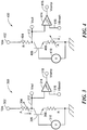
- an example of an electronic circuit 100 can be used in a magnetic field sensor.
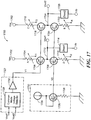
- the electronic circuit 100 can include a fixed resistor 106 having first and second terminals, wherein the first terminal of the resistor 106 is coupled to receive a voltage 102 and the second terminal of the resistor 106 is coupled to an emitter of a PNP bipolar transistor 108.
- the electronic circuit 100 can include a voltage source 104 having first and second terminals, wherein the first terminal of the voltage source 104 is coupled to receive the voltage 102 and the second terminal of the voltage source 104 is coupled to a base of the PNP bipolar transistor 108.
- the electronic circuit 100 can also include a magnetoresistance element 110 having first and second terminals, wherein the first terminal of the magnetoresistance element 110 is coupled to a collector of the PNP bipolar transistor 108 and the second terminal of the magnetoresistance element 110 is coupled to a voltage reference, for example, a ground voltage.
- An output voltage 112 can be generated at the collector of the PNP bipolar transistor 108.
- the electronic circuit 100 can include a comparator 114 having first and second input terminals, wherein a first input terminal of the comparator 114 is coupled to the collector of the PNP bipolar transistor 108 and the second input terminal of the comparator 114 is coupled to receive a threshold voltage 116.
- the comparator 114 can be configured to generate a comparison signal 118.
- the comparison signal 118 can have two states.
- the associated electronic circuits form an electronic switch, wherein a state of the comparison signal 118 is determined by a strength of a magnetic field experienced by the magnetoresistance element 110. It should also be understood that embodiments shown below that are not shown to include a comparator can be adapted to use a comparator to provide an electronic switch.
- the voltage source 104, the resistor 106, and the PNP bipolar transistor 108 form a current source operable to provide a fixed current, I, to the magnetoresistance element 110.
- the output voltage 112 is generated according to the following relationships. In this and in all equations that follow in conjunction with other figures below, a base current of bipolar transistors is relatively small and is disregarded.
- the electronic circuit 200 can include a magnetoresistance element 206 having first and second terminals, wherein the first terminal of the magnetoresistance element 206 is coupled to receive a voltage 202 and the second terminal of the magnetoresistance element 206 is coupled to an emitter of a PNP bipolar transistor 208.
- the electronic circuit 200 can include a voltage source 204 having first and second terminals, wherein the first terminal of the voltage source 204 is coupled to receive the voltage 202 and the second terminal of the voltage source 104 is coupled to a base of the PNP bipolar transistor 208.
- the electronic circuit 200 can include a resistor 210 having first and second terminals, wherein the first terminal of the resistor 210 is coupled to a collector of the PNP bipolar transistor 208 and the second terminal of the resistor 210 is coupled to a voltage reference, for example, a ground voltage.
- An output voltage 212 can be generated at the collector of the PNP bipolar transistor 208.
- the electronic circuit 200 can include a comparator 214 having first and second input terminals, wherein a first input terminal of the comparator 214 is coupled to the collector of the PNP bipolar transistor 208 and the second input terminal of the comparator 214 is coupled to receive a threshold voltage 216.
- the comparator 214 can be configured to generate a comparison signal 218.
- the voltage source 204, the magnetoresistance element 206, and the PNP bipolar transistor 208 form a variable current source operable to provide a variable current, I, to the resistor 110.
- the variable current, I varies in accordance with a variable resistance of the magnetoresistance element 206, which varies in accordance with a sensed magnetic field.
- the electronic circuit 300 can include a magnetoresistance element 304 having first and second terminals, wherein the first terminal of the magnetoresistance element 304 is coupled to receive a voltage 302 and the second terminal of the magnetoresistance element 304 is coupled to a collector of an NPN bipolar transistor 306.
- the electronic circuit 300 can include a resistor 308 having first and second terminals, wherein the first terminal of the resistor 308 is coupled to an emitter of the NPN bipolar transistor 306 and the second terminal of the resistor 308 is coupled to a reference voltage, for example, a ground reference voltage.
- the electronic circuit 300 can include a voltage source 310 having first and second terminals, wherein the first terminal of the voltage source 310 is coupled to a base of the NPN bipolar transistor 306 and the second terminal of the voltage source 310 is coupled to the second terminal of the resistor 308.
- An output voltage 312 can be generated at the collector of the NPN bipolar transistor 306.
- the electronic circuit 300 can include a comparator 314 having first and second input terminals, wherein a first input terminal of the comparator 314 is coupled to the collector of the NPN bipolar transistor 306 and the second input terminal of the comparator 314 is coupled to receive a threshold voltage 316.
- the comparator 314 can be configured to generate a comparison signal 318.
- the voltage source 310, the resistor 308, and the NPN bipolar transistor 306 form a current sink operable to provide a fixed current, I, to the magnetoresistance element 304.
- the electronic circuit 400 can include a resistor 404 having first and second terminals, wherein the first terminal of the resistor 404 is coupled to receive a voltage 402 and the second terminal of the resistor 404 is coupled to a collector of an NPN bipolar transistor 406.
- the electronic circuit 400 can include a magnetoresistance element 408 having first and second terminals, wherein the first terminal of the magnetoresistance element 408 is coupled to an emitter of the NPN bipolar transistor 406 and the second terminal of the magnetoresistance element 408 is coupled to a reference voltage, for example, a ground reference voltage.
- the electronic circuit 400 can include a voltage source 410 having first and second terminals, wherein the first terminal of the voltage source 410 is coupled to a base of the NPN bipolar transistor 408 and the second terminal of the voltage source 410 is coupled to the second terminal of the magnetoresistance element 408
- An output voltage 412 can be generated at the collector of the NPN bipolar transistor 406.
- the electronic circuit 400 can include a comparator 414 having first and second input terminals, wherein a first input terminal of the comparator 414 is coupled to the collector of the NPN bipolar transistor 406 and the second input terminal of the comparator 414 is coupled to receive a threshold voltage 416.
- the comparator 414 can be configured to generate a comparison signal 418.
- the voltage source 410, the magnetoresistance element 408, and the NPN bipolar transistor 406 form a variable current sink operable to provide a variable current, I, to the resistor 404.
- the variable current, I varies in accordance with a variable resistance of the magnetoresistance element 408, which varies in accordance with a sensed magnetic field.
- the electronic circuit 500 can include a magnetoresistance element 506 having first and second terminals, wherein the first terminal of the magnetoresistance element 506 is coupled to receive a voltage 502 and the second terminal of the magnetoresistance element 506 is coupled to an emitter of a PNP bipolar transistor 508.
- the electronic circuit 500 can include a voltage source 504 having first and second terminals, wherein the first terminal of the voltage source 504 is coupled to receive the voltage 502 and the second terminal of the voltage source 504 is coupled to a base of the PNP bipolar transistor 508.
- the electronic circuit 500 can include a resistor 514 having first and second terminals, wherein the first terminal of the resistor 514 is coupled to an emitter of an NPN bipolar transistor 510 and the second terminal of the resistor 514 is coupled to a voltage reference, for example, a ground voltage.
- the electronic circuit 500 can include another voltage source 512 having first and second terminals, wherein the first terminal of the voltage source 512 is coupled a base of the NPN bipolar transistor 510 and the second terminal of the voltage source 512 is coupled to the second terminal of the resistor 514.
- a collector of the PNP bipolar transistor 508 can be coupled to a collector of the NPN bipolar transistor 510 at a junction node.
- a load 518 which can be a resistive or a complex load, can be coupled between the junction node and a bias voltage, Vb. Current can flow into and/or out of the load 518.
- the load 518 is labeled Zload.
- Zload used here and in figures below is not intended to limit the load 518 or loads discussed below to one or more passive electronic components. Instead, the load 518 and loads discussed below can be comprised of passive electronic components, active electronic components, or both.
- An output voltage 516 can be generated at the collector of the PNP bipolar transistor 508 (i.e., at the junction node).
- the electronic circuit 500 can include a comparator coupled to the junction node that is the same as or similar to the comparators shown above in conjunction with FIGS. 1-4 .
- the voltage source 504, the magnetoresistance element 506, and the PNP bipolar transistor 508 form a variable current source operable to provide a variable current, 11.
- the variable current, I1 varies in accordance with a variable resistance of the magnetoresistance element 506, which varies in accordance with a sensed magnetic field.
- the voltage source 512, the resistor 514, and the NPN bipolar transistor 510 form a current sink operable to provide a fixed current, 12.
- the load 518 can be made to have a high impedance to achieve a gain not obtained with the electronic circuits of FIGS. 1-4 described above.
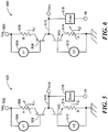
- the electronic circuit 600 can include a resistor 606 having first and second terminals, wherein the first terminal of the resistor 606 is coupled to receive a voltage 602 and the second terminal of the resistor 606 is coupled to an emitter of a PNP bipolar transistor 608.
- the electronic circuit 600 can include a voltage source 604 having first and second terminals, wherein the first terminal of the voltage source 604 is coupled to receive the voltage 602 and the second terminal of the voltage source 604 is coupled to a base of the PNP bipolar transistor 608.
- the electronic circuit 600 can include a magnetoresistance element 614 having first and second terminals, wherein the first terminal of the magnetoresistance element 614 is coupled to an emitter of an NPN bipolar transistor 610 and the second terminal of the magnetoresistance element 614 is coupled to a voltage reference, for example, a ground voltage.
- the electronic circuit 600 can include another voltage source 612 having first and second terminals, wherein the first terminal of the voltage source 612 is coupled a base of the NPN bipolar transistor 610 and the second terminal of the voltage source 612 is coupled to the second terminal of the magnetoresistance element 614.
- a collector of the PNP bipolar transistor 608 can be coupled to a collector of the NPN bipolar transistor 610 at a junction node.
- a load 618 which can be a resistive or a complex load, can be coupled between the junction node and a bias voltage, Vb. Current can flow into and/or out of the load 618.
- the load 618 is labeled Zload.
- Zload used here and in figures below is not intended to limit the load 618 or loads discussed below to one or more passive electronic components. Instead, the load 618 and loads discussed below can be comprised of passive electronic components, active electronic components, or both.
- An output voltage 616 can be generated at the collector of the PNP bipolar transistor 608 (i.e., at the junction node).
- the electronic circuit 600 can include a comparator coupled to the junction node that is the same as or similar to the comparators shown above in conjunction with FIGS. 1-4 .
- Other electronic circuits described below can also include a comparator, though not shown.
- the voltage source 604, the resistor 606, and the PNP bipolar transistor 608 form a current source operable to provide a fixed current, I1. It should be appreciated that the voltage source 612, the magnetoresistance element 614, and the NPN bipolar transistor 610 form a variable current sink operable to provide a variable current, 12.
- the variable current, 12, varies in accordance with a variable resistance of the magnetoresistance element 614, which varies in accordance with a sensed magnetic field.
- the load 618 can be made to have a high impedance to achieve a gain not obtained with the electronic circuits of FIGS. 1-4 described above.
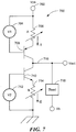
- the electronic circuit 700 can include a magnetoresistance element 706 having first and second terminals, wherein the first terminal of the magnetoresistance element 706 is coupled to receive a voltage 702 and the second terminal of the magnetoresistance element 706 is coupled to an emitter of a PNP bipolar transistor 708.
- the electronic circuit 700 can include a voltage source 704 having first and second terminals, wherein the first terminal of the voltage source 704 is coupled to receive the voltage 702 and the second terminal of the voltage source 704 is coupled to a base of the PNP bipolar transistor 708.
- the electronic circuit 700 can include another magnetoresistance element 714 having first and second terminals, wherein the first terminal of the magnetoresistance element 714 is coupled to an emitter of an NPN bipolar transistor 710 and the second terminal of the magnetoresistance element 714 is coupled to a voltage reference, for example, a ground voltage.
- the electronic circuit 700 can include another voltage source 712 having first and second terminals, wherein the first terminal of the voltage source 712 is coupled a base of the NPN bipolar transistor 710 and the second terminal of the voltage source 712 is coupled to the second terminal of the magnetoresistance element 714.
- a collector of the PNP bipolar transistor 708 can be coupled to a collector of the NPN bipolar transistor 710 at a junction node.
- a load 718 which can be a resistive or a complex load, can be coupled between the junction node and a bias voltage, Vb. Current can flow into and/or out of the load 718.
- the load 718 is labeled Zload.
- Zload used here and in figures below is not intended to limit the load 718 or loads discussed below to one or more passive electronic components. Instead, the load 718 and loads discussed below can be comprised of passive electronic components, active electronic components, or both.
- An output voltage 716 can be generated at the collector of the PNP bipolar transistor 708 (i.e., at the junction node).
- the electronic circuit 700 can include a comparator coupled to the junction node that is the same as or similar to the comparators shown above in conjunction with FIGS. 1-4 .
- Other electronic circuits described below can also include a comparator, though not shown or described below.
- the voltage source 704, the magnetoresistance element 706, and the PNP bipolar transistor 708 form a variable current source operable to provide a variable current, I1.
- the variable current, I1 varies in accordance with a variable resistance of the magnetoresistance element 706, which varies in accordance with a sensed magnetic field.
- the voltage source 712, the magnetoresistance element 714, and the NPN bipolar transistor 710 form a variable current sink operable to provide a variable current, 12.
- the variable current, 12, varies in accordance with a variable resistance of the magnetoresistance element 714, which varies in accordance with a sensed magnetic field.
- the load 718 can be made to have a high impedance to achieve a gain not obtained with the electronic circuits of FIGS. 1-4 described above.
- noises of the two magnetoresistance elements 706, 714 add incoherently to result in the square root of two times the noise of one magnetoresistance element.
- signals resulting from resistance changes of the two magnetoresistance elements 706, 714 add coherently to result in an output signal 716 two times a signal that would result from one magnetoresistance element, for example, as provided by the electronic circuits of FIGS. 1-6 .
- a signal to noise ratio improvement is obtained. Similar improvements in signal to noise ratio can be obtained for similar reasons with circuits described below.
- the same current, 11 flows through the PNP bipolar transistor 708 and through the magnetoresistance element 706.
- the same current, 12 flows through the NPN bipolar transistor 710 and through the magnetoresistance element 714.
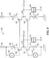
- the electronic circuit 800 can include a magnetoresistance element 806 having first and second terminals, wherein the first terminal of the magnetoresistance element 806 is coupled to receive a voltage 802 and the second terminal of the magnetoresistance element 806 is coupled to an emitter of a PNP bipolar transistor 808.
- the electronic circuit 800 can include a voltage source 804 having first and second terminals, wherein the first terminal of the voltage source 804 is coupled to receive the voltage 802 and the second terminal of the voltage source 804 is coupled to a base of the PNP bipolar transistor 808.
- the electronic circuit 800 can include a resistor 814 having first and second terminals, wherein the first terminal of the resistor 814 is coupled to an emitter of an NPN bipolar transistor 810 and the second terminal of the resistor 814 is coupled to a voltage reference, for example, a ground voltage.
- the electronic circuit 800 can include another voltage source 812 having first and second terminals, wherein the first terminal of the voltage source 812 is coupled a base of the NPN bipolar transistor 810 and the second terminal of the voltage source 812 is coupled to the second terminal of the resistor 814.
- a collector of the PNP bipolar transistor 808 can be coupled to a collector of the NPN bipolar transistor 810 at a junction node.
- a load 818 which can be a resistive or a complex load, can be coupled between the junction node and the second terminal of the resistor 814.
- An output voltage 816 can be generated at the collector of the PNP bipolar transistor 808 (i.e., at the junction node).
- the voltage source 804, the magnetoresistance element 806, and the PNP bipolar transistor 808 form a variable current source operable to provide a variable current, 11.
- the variable current, 11, varies in accordance with a variable resistance of the magnetoresistance element 806, which varies in accordance with a sensed magnetic field.
- the voltage source 812, the resistor 814, and the NPN bipolar transistor 810 form a current sink operable to provide a fixed current, 12.
- I1 flows through the PNP bipolar transistor 808 and through the magnetoresistance element 806.
- the electronic circuit 800 can also include a resistor 820 having first and second terminals, wherein the first terminal of the resistor 820 is coupled to receive the voltage 802 and the second terminal of the resistor 820 is coupled to an emitter of a PNP bipolar transistor 822.
- the second terminal of the voltage source 804 can be coupled to a base of the PNP bipolar transistor 822.
- the electronic circuit 800 can include a magnetoresistance element 826 having first and second terminals, wherein the first terminal of the magnetoresistance element 826 is coupled to an emitter of an NPN bipolar transistor 824 and the second terminal of the magnetoresistance element 826 is coupled to a voltage reference, for example, a ground voltage.
- the first terminal of the voltage source 812 is coupled a base of the NPN bipolar transistor 824.
- a collector of the PNP bipolar transistor 822 can be coupled to a collector of the NPN bipolar transistor 824 at a junction node.
- a load 830 which can be a resistive or a complex load, can be coupled between the junction node and the second terminal of the magnetoresistance element 826.
- An output voltage 828 can be generated at the collector of the PNP bipolar transistor 822 (i.e., at the junction node).
- the voltage source 804, the resistor 820, and the PNP bipolar transistor 822 form a current source operable to provide a fixed current, I3. It should be appreciated that the voltage source 812, the magnetoresistance element 826, and the NPN bipolar transistor 824 form a variable current sink operable to provide a variable current, 14.
- the variable current, 14, varies in accordance with a variable resistance of the magnetoresistance element 826, which varies in accordance with a sensed magnetic field.
- the loads 818, 830 can be made to have high impedances to achieve single ended gains not obtained with the electronic circuits of FIGS. 1-4 described above. Furthermore, the above described differential signal has an amplitude that is double the amplitude of the single ended signals.
- a magnetic field sensor 900 can include a substrate 902 having a surface 902a, which is one of two parallel major surfaces of the substrate 902.
- Two magnetoresistance elements 904, 906 can be disposed upon the surface 902a along an axis 908.
- the two magnetoresistance elements 904, 906 (A, B) can be part of or coupled to an electronic circuit 910, which is also disposed upon or within the surface 902a of the substrate 902.
- the two magnetoresistance elements 904, 906 (A, B) can be the same as or similar to the magnetic field sensing elements 706, 714 of FIG. 7 and the two magnetoresistance element 806, 812 of FIG. 3-8 .
- the designations A, B can also be found in FIGS. 7 and 8 to represent resistance values.
- Magnetoresistance elements e.g., 904, 906 (A, B) are shown in all embodiments herein to be in the form of so-called "yokes," which have a C-shape (or a reverse C-shape).
- the yokes can have longest yoke axes substantially perpendicular to the axis 908.
- Advantages of yoke shapes are known. It will be understood that other magnetoresistance elements used in embodiments herein can have other shapes, for example, lines, polylines, or rectangles.
- Maximum response axes of the magnetoresistance elements 904, 906 (A, B) can be parallel to and along the axis 908 and in the same direction. It should be understood that the magnetoresistance elements 904, 906 (A, B) having maximum response axes parallel to the axis 908 are also responsive to magnetic fields at other angles in the plane of the substrate 902 (and also out of the plane of the substrate 902). The degree to which the magnetoresistance elements 904, 906 (A, B) are responsive to magnetic fields at other angles not parallel to the axis 908 (and not perpendicular to the longest yoke axes) is determined by a magnitude of a geometric projection of the magnetic field at the other angle onto the axis 908. Thus, the term "projected magnetic field" is used below to describe this projection.
- the yoke shapes of the magnetoresistance elements 904, 906 may be rotated so that the longest yokes axes are not perpendicular to the axis 908, the degree to which the magnetoresistance elements 904, 906 (A, B) are responsive to magnetic fields at other angles not parallel to the axis 908 is determined by a magnitude of a geometric projection of the magnetic field at the other angle onto an axis that is perpendicular to the longest axes of the yoke shapes. This is also referred to herein as a projected magnetic field.
- the magnetic field sensor 900 is responsive to movement of a ferromagnetic target object 912 having features, e.g., 912a, with width 914.
- the ferromagnetic target 912 object can be, for example, a gear having gear teeth, in which case, the feature 912a of the gear can be one of a plurality of gear teeth or one of a plurality of gear valleys.
- the ferromagnetic target object 912 can be a multi-pole ring magnet having alternating north and south poles, in which case, the feature 912a can be one of a plurality of magnetic poles, for example, a north pole or a south pole.
- the two magnetoresistance elements 904, 906 have a separation 916 between about one half and about one and one half of the width 914 of the target feature 912a, for example, a gear tooth of a ferromagnetic gear or a magnetic domain of a ferromagnetic ring magnet.
- the two magnetoresistance elements 904, 906 (A, B) have a separation 916 between about one half and about twice the width 914 of the target feature 912a.
- the separation 916 is much smaller than half of the width 914, for example, one one hundredth of the width 914, or larger than twice the width 914.
- the separation 916 is about equal to the width 914 of the target feature 912a, for example, a gear tooth of a ferromagnetic gear or a magnetic domain of a ferromagnetic ring magnet.
- the two magnetoresistance elements 904, 906 can generate two output signals.
- FIGS. 7 and 8 above are representative of ways in which the two magnetic field sensing elements 904, 906 can generate two output signals.
- the designation A and B are indicative of resistances and are also indicative of physical placement in relation to FIG. 9 .
- the target feature 912a with a width 914 equal to the spacing 916 between the two magnetoresistance elements 904, 906 (A, B) when the target feature 912a is centered about (i.e., between) the two magnetoresistance elements 904, 906 (A, B), it can be shown that any magnetoresistance element(s) (e.g., 904 (A)) on one side of a center of the target feature 912a experience a projected magnetic field pointed in one direction along the axis 908, and any magnetoresistance element(s) (e.g., 906 (B)) on the other side of the center of the target feature 912a experience a projected magnetic field pointed in the other direction.
- any magnetoresistance element(s) e.g., 904 (A)
- any magnetoresistance element(s) e.g., 906 (B)
- any magnetoresistance element(s) e.g., 904 (A)
- any magnetoresistance element(s) e.g., 906 (B)
- any magnetoresistance element(s) e.g., 906 (B)
- the electronic circuit 700 of FIG. 7 can operate as a so-called “edge detector,” generating a largest voltage 716 when the two magnetoresistance elements 706, 714 are on opposite sides of an edge of the feature 912a.
- the electronic circuit 800 of FIG. 8 can operate as a so-called “feature detector,” generating a largest differential signal Vout1-Vout2 when the two magnetoresistance elements 806, 826 are on opposite sides of a center of the feature 912a.
- the magnetic field sensor 900 can include a magnet.
- the electronic circuit 1000 can include a magnetoresistance element 1006 having first and second terminals, wherein the first terminal of the magnetoresistance element 1006 is coupled to receive a voltage 1002 and the second terminal of the magnetoresistance element 1006 is coupled to an emitter of a PNP bipolar transistor 1008.
- the electronic circuit 1000 can include a voltage source 1004 having first and second terminals, wherein the first terminal of the voltage source 1004 is coupled to receive the voltage 1002 and the second terminal of the voltage source 1004 is coupled to a base of the PNP bipolar transistor 1008.
- the electronic circuit 1000 can include another magnetoresistance element 1014 having first and second terminals, wherein the first terminal of the magnetoresistance element 1014 is coupled to an emitter of an NPN bipolar transistor 1010 and the second terminal of the magnetoresistance element 1014 is coupled to a voltage reference, for example, a ground voltage.
- the electronic circuit 1000 can include another voltage source 1012 having first and second terminals, wherein the first terminal of the voltage source 1012 is coupled a base of the NPN bipolar transistor 1010 and the second terminal of the voltage source 1012 is coupled to the second terminal of the magnetoresistance element 1014.
- a collector of the PNP bipolar transistor 1008 can be coupled to a collector of the NPN bipolar transistor 1010 at a junction node.
- a load 1018 which can be a resistive or a complex load, can be coupled between the junction node and a bias voltage, Vb. Current can flow into and/or out of the load 1018.
- the load 1018 is labeled Zload1.
- the nomenclature, Zloadl, used here and in figures below is not intended to limit the load 1018 or loads discussed below to one or more passive electronic components. Instead, the load 1018 and loads discussed below can be comprised of passive electronic components, active electronic components, or both.
- An output voltage 1016 can be generated at the collector of the PNP bipolar transistor 1008 (i.e., at the junction node).
- the voltage source 1004, the magnetoresistance element 1006, and the PNP bipolar transistor 1008 form a variable current source operable to provide a variable current, 11.
- the variable current, I1 varies in accordance with a variable resistance of the magnetoresistance element 1006, which varies in accordance with a sensed magnetic field.
- variable current sink operable to provide a variable current, I2.
- the variable current, I2 varies in accordance with a variable resistance of the magnetoresistance element 1014, which varies in accordance with a sensed magnetic field.
- the same current, I1 flows through the PNP bipolar transistor 1008 and through the magnetoresistance element 1006.
- I2, (different than I1) flows through the NPN bipolar transistor 1010 and through the magnetoresistance element 1014.
- the electronic circuit 1000 can also include a magnetoresistance element 1020 having first and second terminals, wherein the first terminal of the magnetoresistance element 1020 is coupled to receive the voltage 1002 and the second terminal of the magnetoresistance element 1020 is coupled to an emitter of a PNP bipolar transistor 1022.
- the second terminal of the voltage source 1004 can be coupled to a base of the PNP bipolar transistor 1022.
- the electronic circuit 1000 can include another magnetoresistance element 1026 having first and second terminals, wherein the first terminal of the magnetoresistance element 1026 is coupled to an emitter of an NPN bipolar transistor 1024 and the second terminal of the magnetoresistance element 1026 is coupled to a voltage reference, for example, a ground voltage.
- the first terminal of the voltage source 1012 is coupled a base of the NPN bipolar transistor 1024.
- a collector of the PNP bipolar transistor 1022 can be coupled to a collector of the NPN bipolar transistor 1024 at a junction node.
- a load 1030 which can be a resistive or a complex load, can be coupled between the junction node and a bias voltage, Vb. Current can flow into and/or out of the load 1030.
- the load 1030 is labeled Zload2.
- Zload2 used here and in figures below is not intended to limit the load 1030 or loads discussed below to one or more passive electronic components. Instead, the load 1030 and loads discussed below can be comprised of passive electronic components, active electronic components, or both.
- An output voltage 1028 can be generated at the collector of the PNP bipolar transistor 1022 (i.e., at the junction node).
- the voltage source 1004, the magnetoresistance element 1020, and the PNP bipolar transistor 1022 form a current source operable to provide a variable current, I3.
- the variable current, I3, varies in accordance with a variable resistance of the magnetoresistance element 1020, which varies in accordance with a sensed magnetic field.
- the voltage source 1012, the magnetoresistance element 1026, and the NPN bipolar transistor 1024 form a variable current sink operable to provide a variable current, I4.
- the variable current, I4 varies in accordance with a variable resistance of the magnetoresistance element 1026, which varies in accordance with a sensed magnetic field.
- the same current, 13, (different than I1, I2) flows through the PNP bipolar transistor 1022 and through the magnetoresistance element 1020.
- the same current, I4, (different than I1, I2, I3) flows through the NPN bipolar transistor 1024 and through the magnetoresistance element 1026.
- the loads 1018, 1030 can be made to have high impedances to achieve single ended gains not obtained with the electronic circuits of FIGS. 1-4 described above. Furthermore, the above described differential signal has an amplitude that is double the amplitude of the single ended signals.
- the voltage source 1012 of FIG. 10 is replaced with a circuit portion 1102, which will be recognized to be a reference leg of a current mirror.
- the circuit portion 1102 can include a current source 1104 having an output node.
- a collector of an NPN bipolar transistor 1106 can be coupled to the current source.
- a base of the NPN bipolar transistor 1106 can be coupled to the collector of the NPN bipolar transistor 1106, such that the NPN bipolar transistor operates merely as a diode.
- a resistor 1180 having first and second terminals can be coupled such that the first terminal of the resistor is coupled to an emitter of the NPN bipolar transistor 1106 and the second terminal of the resistor 1108 is coupled to a reference voltage, for example, a ground voltage.
- the base or the NPN bipolar transistor 1106 is coupled to the bases of the NPN bipolar transistors 1010, 1024,
- the electronic circuit 1100 operates in substantially the same way as the electronic circuit 1000 of FIG. 10 , and has the same operating equations.
- FIG. 12 in which like elements of FIGS. 10 and 11 are shown having like reference designations, in an electronic circuit 1200, the voltage source 1004 of FIGS. 10 and 11 is replaced with a circuit portion 1202, which operates as a common mode voltage detector.
- the circuit portion 1202 can include a common mode voltage detector 1204 coupled to receive the two output voltages 1016, 1028 and operable to generate a common mode detection signal 1204a indicative of a common mode voltage of the output voltages 1016, 1028.
- a voltage buffer or level translator 1206 can be coupled to receive the common mode detection signal 1204a and operable to generate a signal coupled to the bases of the PNP bipolar transistors 1008, 1022.
- the common mode voltage detector 1204 can detect the error condition and adjust the current flowing through the two PNP bipolar transistors 1008, 1022 to remove the error condition.
- the electronic circuit 1200 operates in substantially the same way as the electronic circuit 1000 of FIG. 10 and the electronic circuit 1100 of FIG. 1 , and has the same operating equations.
- a magnetic field sensor 1300 can include a substrate 1302 having a surface 1302a, which is one of two parallel major surfaces of the substrate 1302.
- magnetoresistance elements 1304, 1306, 1308, 1310 can be disposed upon the surface 1302a along an axis 1314.
- the four magnetoresistance elements 1304, 1306, 1308, 1310 can be part of or coupled to an electronic circuit 1312, which is also disposed upon or within the surface 1302a of the substrate 1302.
- the four magnetoresistance elements 1304, 1306, 1308, 1310 can be the same as or similar to the magnetic field sensing elements 1006, 1026, 1020, 1014, respectively, of FIGS. 10 and 11 .
- Maximum response axes of the four magnetoresistance elements 1304, 1306, 1308, 1310 can be parallel to and along an axis 1314, and in the same direction. Angles of magnetic fields are discussed above in conjunction with FIG. 9 .
- the magnetic field sensor 1300 is responsive to movement of the ferromagnetic target object 912.
- the four magnetoresistance elements 1304, 1306, 1308, 1310 are disposed along the axis 1314 proximate to the ferromagnetic target object 912.
- the two magnetoresistance elements 1304, 1308 (A, C) have a separation 1320 between about one half and about one and one half of the width 914 of the target feature 912a, for example, a gear tooth of a ferromagnetic gear or a magnetic domain of a ferromagnetic ring magnet.
- the two magnetoresistance elements 1304, 1308 (A, C) have a separation 1320 between about one half and about twice the width 914 of the target feature 912a.
- the separation 1320 is much smaller than half of the width 914, for example, one one hundredth of the width 914 or larger than twice the width 914.
- the separation 1320 is about equal to the width 914 of the target feature 912a.
- the two magnetoresistance elements 1306, 1310 (B, D) have a separation 1322 between about one half and about one and one half of the width 914 of the target feature 912a, for example, a gear tooth of a ferromagnetic gear or a magnetic domain of a ferromagnetic ring magnet.
- the two magnetoresistance elements 1306, 1310 (B, D) have a separation 1322 between about one half and about twice the width 914 of the target feature 912a.
- the separation 1322 is much smaller than half of the width 914, for example, one one hundredth of the width 914 or larger than twice the width 914.
- the separation 1322 is about equal to the width 914 of the target feature 912a.
- the two magnetoresistance elements 1304, 1306 (A, B) have a separation 1324 between about one half and about one and one half of the width 914 of the target feature 912a. In some other embodiments, the two magnetoresistance elements 1304, 1306 (A, B) have a separation 1324 between about one half and about twice the width 914 of the target feature 912a. However, in other embodiments, the separation 1324 is much smaller than half of the width 914, for example, one one hundredth of the width 914 or larger than twice the width 914.
- the separation 1324 is about equal to the width 914 of the target feature 912a.
- the two magnetoresistance elements 1308, 1310 (C, D) have a separation 1326 between about one half and about one and one half of the width 914 of the target feature 912a. In some other embodiments, the two magnetoresistance elements 1308, 1310 (C, D) have a separation 1326 between about one half and twice the width 914 of the target feature 912a. However, in other embodiments, the separation 1326 is much smaller than half of the width 914, for example, one one hundredth of the width 914 or larger than twice the width 914.
- the separation 1326 is about equal to the width 914 of the target feature 912a.
- the four magnetoresistance elements 1304, 1306, 1308, 1310 can generate at least two output signals.
- FIGS. 10 , 11 , and 12 above are representative of ways in which the four magnetoresistance elements 1304, 1306, 1308, 1310 (A, B, C, D) can generate at least two output signals.
- the designation A, B, C, and D are indicative of resistances and are also indicative of physical placement in relation to FIG. 13 .
- the target feature 912a with a width 914 equal to the spacings 1320, 1322, when the target feature 912a is centered about (i.e., between) the four magnetoresistance elements 1304, 1306, 1308, 1310 (A, B, C, D), it can be shown that any magnetoresistance element(s) (e.g., 1304, 1306 (A, B)) on one side of a center of the target feature 912a experiences a projected magnetic field pointed in one direction along the axis 1314, and any magnetoresistance element(s) (e.g., 1308, 1310 (C, D)) on the other side of the center of the target feature 912a experiences a projected magnetic field pointed in the other direction.
- any magnetoresistance element(s) e.g., 1304, 1306 (A, B)
- any magnetoresistance element(s) e.g., 1308, 1310 (C, D)
- any magnetoresistance element(s) e.g., 1304, 1306 (A, B)
- any magnetoresistance element(s) e.g., 1308, 1310 (C, D)
- any magnetoresistance element(s) e.g., 1308, 1310 (C, D)
- the two magnetoresistance elements 1306, 1308 (B, C) experience projected magnetic fields pointed in the same direction along the axis 1314, but opposite in direction from the projected magnetic fields experienced by the two magnetoresistance elements 1304, 1310 (A, D).
- resistance of both of the two magnetoresistance elements 1306, 1308 (B, C) change in the same direction but opposite to the resistance change of the two magnetoresistance elements 1304, 1310 (A, D).
- the electronic circuits 1000, 1100, 1200 of FIGS. 10 , 11 , 12 can operate as a feature detectors, generating a largest differential voltage Vout1-Vout2 when the four magnetoresistance elements 1004 (A), 1026 (B), 1020 (C), 1014 (D) of FIGS. 10 , 11 , 12 are arranged as shown in FIG. 13 by designations A-D, arranged relative to a center of the target feature 912a.
- the magnetic field sensor 1400 can include a magnet.
- the electronic circuit 1400 can include a magnetoresistance element 1404 having first and second terminals, wherein the first terminal of the magnetoresistance element 1404 is coupled to receive a voltage 1402 and the second terminal of the magnetoresistance element 1404 is coupled to an emitter of a PNP bipolar transistor 1406.
- the electronic circuit 1400 can include a voltage source in the form of a common mode voltage detector circuit 1435 coupled to the base of the PNP bipolar transistor 1406.
- the electronic circuit 1400 can include another magnetoresistance element 1410 having first and second terminals, wherein the first terminal of the magnetoresistance element 1410 is coupled to an emitter of an NPN bipolar transistor 1408 and the second terminal of the magnetoresistance element 1410 is coupled to a voltage reference, for example, a ground voltage.
- the electronic circuit 1400 can include a voltage source in the form of a current mirror reference leg 1428 coupled to the base of the NPN bipolar transistor 1408.
- a collector of the PNP bipolar transistor 1406 can be coupled to a collector of the NPN bipolar transistor 1408 at a junction node.
- a load 1414 which can be a resistive or a complex load, can be coupled between the junction node and a bias voltage, Vb. Current can flow into and/or out of the load 1414.
- the load 1414 is labeled Z1.
- the nomenclature, Z1 is not intended to limit the load 1414 to one or more passive electronic components. Instead, the load 1414 can be comprised of passive electronic components, active electronic components, or both.
- An output voltage 1412 can be generated at the collector of the PNP bipolar transistor 1406 (i.e., at the junction node).
- the electronic circuit 1400 can also include a magnetoresistance element 1416 having first and second terminals, wherein the first terminal of the magnetoresistance element 1416 is coupled to receive the voltage 1402 and the second terminal of the magnetoresistance element 1416 is coupled to an emitter of a PNP bipolar transistor 1418.
- the common mode voltage detector circuit 1435 can be coupled to a base of the PNP bipolar transistor 1418.
- the electronic circuit 1400 can include another magnetoresistance element 1422 having first and second terminals, wherein the first terminal of the magnetoresistance element 1422 is coupled to an emitter of an NPN bipolar transistor 1420 and the second terminal of the magnetoresistance element 1422 is coupled to a voltage reference, for example, a ground voltage.
- the current mirror reference leg 1428 is coupled to a base of the NPN bipolar transistor 1420.
- a collector of the PNP bipolar transistor 1418 can be coupled to a collector of the NPN bipolar transistor 1420 at a junction node.
- a load 1426 which can be a resistive or a complex load, can be coupled between the junction node and a bias voltage, Vb. Current can flow into and/or out of the load 1426
- the load 1426 is labeled Z2.
- the nomenclature, Z2 is not intended to limit the load 1426 to one or more passive electronic components. Instead, the load 1426 can be comprised of passive electronic components, active electronic components, or both.
- An output voltage 1424 can be generated at the collector of the PNP bipolar transistor 1418 (i.e., at the junction node).
- the same current, 13, (different than I1, I2) flows through the PNP bipolar transistor 1418 and through the magnetoresistance element 1416.
- the same current, I4, (different than I1, I2, I3) flows through the NPN bipolar transistor 1024 and through the magnetoresistance element 1422.
- the output voltages 1412, 1424 can be taken individually (i.e. single ended signals).
- the loads 1414, 1426 can be made to have high impedances to achieve single ended gains not obtained with the electronic circuits of FIGS. 1-4 described above. Furthermore, the above described differential signal has an amplitude that is double the amplitude of the single ended signals.
- the electronic circuit 1400 can also include a magnetoresistance element 1440 having first and second terminals, wherein the first terminal of the magnetoresistance element 1440 is coupled to receive a voltage 1402 and the second terminal of the magnetoresistance element 1440 is coupled to an emitter of a PNP bipolar transistor 1442.
- the electronic circuit 1400 can include a common mode voltage detector circuit 1471 coupled to a base of the PNP bipolar transistor 1442.
- the electronic circuit 1400 can include another magnetoresistance element 1446 having first and second terminals, wherein the first terminal of the magnetoresistance element 1446 is coupled to an emitter of an NPN bipolar transistor 1444 and the second terminal of the magnetoresistance element 1446 is coupled to a voltage reference, for example, a ground voltage.
- the electronic circuit 1400 can include a current mirror reference leg 1464 coupled a base of the NPN bipolar transistor 1444.
- a collector of the PNP bipolar transistor 1442 can be coupled to a collector of the NPN bipolar transistor 1444 at a junction node.
- a load 1450 which can be a resistive or a complex load, can be coupled between the junction node and a bias voltage, Vb. Current can flow into and/or out of the load 1450.
- the load 1450 is labeled Z3.
- the nomenclature, Z3, is not intended to limit the load 1450 to one or more passive electronic components. Instead, the load 1450 can be comprised of passive electronic components, active electronic components, or both.
- An output voltage 1448 can be generated at the collector of the PNP bipolar transistor 1442 (i.e., at the junction node).
- the electronic circuit 1400 can also include a magnetoresistance element 1452 having first and second terminals, wherein the first terminal of the magnetoresistance element 1452 is coupled to receive the voltage 1402 and the second terminal of the magnetoresistance element 1452 is coupled to an emitter of a PNP bipolar transistor 1454.
- the common mode voltage detector circuit 1471 can be coupled to a base of the PNP bipolar transistor 1454.
- the electronic circuit 1400 can include another magnetoresistance element 1458 having first and second terminals, wherein the first terminal of the magnetoresistance element 1458 is coupled to an emitter of an NPN bipolar transistor 1456 and the second terminal of the magnetoresistance element 1458 is coupled to a voltage reference, for example, a ground voltage.
- the current mirror reference leg 1464 is coupled to a base of the NPN bipolar transistor 1456.
- a collector of the PNP bipolar transistor 1454 can be coupled to a collector of the NPN bipolar transistor 1456 at a junction node.
- a load 1462 which can be a resistive or a complex load, can be coupled between the junction node and a bias voltage, Vb. Current can flow into and/or out of the load 1462
- the load 1462 is labeled Z4.
- the nomenclature, Z4 is not intended to limit the load 1462 to one or more passive electronic components. Instead, the load 1462 can be comprised of passive electronic components, active electronic components, or both.
- An output voltage 1460 can be generated at the collector of the PNP bipolar transistor 1454 (i.e., at the junction node).
- the output voltages 1448, 1460 can be taken individually (i.e. single ended signals).
- the loads 1450, 1462 can be made to have high impedances to achieve single ended gains not obtained with the electronic circuits of FIGS. 1-4 described above. Furthermore, the above described differential signal has an amplitude that is double the amplitude of the single ended signals.
- the output voltages 1412, 1424, 1448, 1460 can be taken individually (i.e., single ended). However, in other embodiments, the output voltages 1412, 1424, 1448, 1460 can be combined in any way, for example, resulting in two differential signals.
- a magnetic field sensor 1500 can include a substrate 1502 having a surface 1502a, which is one of two parallel major surfaces of the substrate 1502.
- the eight magnetoresistance elements 1504a, 1504b, 1506a, 1506b, 1508a, 1508b, 1510a, 1510b can be disposed upon the surface 1502a along an axis 1514.
- the eight magnetoresistance elements 1504a, 1504b, 1506a, 1506b, 1508a, 1508b, 1510a, 1510b can be part of or coupled to an electronic circuit 1512, which is also disposed upon or within the surface 1502a of the substrate 1502.
- the eight magnetoresistance elements 1504a, 1504b, 1506a, 1506b, 1508a, 1508b, 1510a, 1510b can be the same as or similar to the eight magnetoresistance elements of FIG. 14 .
- Maximum response axes of the eight magnetoresistance elements 1504a, 1504b, 1506a, 1506b, 1508a, 1508b, 1510a, 1510b can be parallel to and along an axis 1514, and in the same direction. Angles of magnetic fields are discussed above in conjunction with FIG. 9 .
- the magnetic field sensor 1500 is responsive to movement of the ferromagnetic target object 912.
- the eight magnetoresistance elements 1504a, 1504b, 1506a, 1506b, 1508a, 1508b, 1510a, 1510b are disposed along the axis 1514 proximate to the ferromagnetic target object 912.
- the two magnetoresistance elements 1504a, 1504b have a separation 1520 to the two magnetoresistance elements 1508a, 1508b (C1, C2) between about one half and about one and one half of the width 914 of the target feature 912a, for example, a gear tooth of a ferromagnetic gear or a magnetic domain of a ferromagnetic ring magnet.
- the two magnetoresistance elements 1504a, 1504b (A1, A2) have a separation 1520 to the two magnetoresistance elements 1508a, 1508b (C1, C2) between about one half and about twice the width 914 of the target feature 912a.
- the separation 1520 is much smaller than half of the width 914, for example, one one hundredth of the width 914, or larger than twice the width 914.
- the separation 1520 is about equal to the width 914 of the target feature 912a.
- the two magnetoresistance elements 1506a, 1506b have a separation 1522 to the two magnetoresistance elements 1510a, 1510b (D1, D2) between about one half and about one and one half of the width 914 of the target feature 912a, for example, a gear tooth of a ferromagnetic gear or a magnetic domain of a ferromagnetic ring magnet.
- the two magnetoresistance elements 1506a, 1506b (B1, B2) have a separation 1522 to the two magnetoresistance elements 1510a, 1510b (D1, D2) between about one half and about twice the width 914 of the target feature 912a.
- the separation 1522 is much smaller than half of the width 914, for example, one one hundredth of the width 914, or larger than twice the width 914.
- the separation 1522 is about equal to the width 914 of the target feature 912a.
- the two magnetoresistance elements 1504a, 1504b have a separation 1524 to the two magnetoresistance elements 1506a, 1506b (B1, B2) between about one half and about one and one half of the width 914 of the target feature 912a.
- the two magnetoresistance elements 1504a, 1504b have a separation 1524 to the two magnetoresistance elements 1506a, 1506b (B1, B2) between about one half and twice the width 914 of the target feature 912a.
- the separation 1524 is much smaller than half of the width 914, for example, one one hundredth of the width 914, or larger than twice the width 914.
- the separation 1524 is about equal to the width 914 of the target feature 912a.
- the two magnetoresistance elements 1508a, 1508b have a separation 1526 to the two magnetoresistance elements 1510a, 1510b (D1, D2) between about one half and about one and one half of the width 914 of the target feature 912a.
- the two magnetoresistance elements 1508a, 1508b have a separation 1526 to the two magnetoresistance elements 1510a, 1510b (D1, D2) between about twice the width 914 of the target feature 912a.
- the separation 1526 is much smaller than half of the width 914, for example, one one hundredth of the width 914, or larger than twice the width 914.
- the separation 1526 is about equal to the width 914 of the target feature 912a.
- the eight magnetoresistance elements 1504a, 1504b, 1506a, 1506b, 1508a, 1508b, 1510a, 1510b can generate at least two output signals.
- FIG. 14 is representative of ways in which the eight magnetoresistance elements 1504a, 1504b, 1506a, 1506b, 1508a, 1508b, 1510a, 1510b (A1, A2, B1, B2, C1, C2, D1, D2) can generate at least two output signals.
- the designations A1, A2, B1, B2, C1, C2, D1, D2 are indicative of resistances and are also indicative of physical placement in relation to FIG. 15 .
- the target feature 912a with a width 914 equal to the spacings 1520, 1522
- the target feature 912a is centered about (i.e., between) the eight magnetoresistance elements 1504a, 1504b, 1506a, 1506b, 1508a, 1508b, 1510a, 1510b (A1, A2, B1, B2, C1, C2, D1, D2)
- any magnetoresistance element(s) e.g., 1504a, 1504b, 1506a, 1506b (A1, A2, B1, B2) on one side of a center of the target feature 912a experiences a projected magnetic field pointed in one direction along the axis 1514
- any magnetoresistance element(s) e.g., 1508a, 1508b, 1510a, 1510b (C1, C2, D1, D1)
- the other side of the center of the target feature 912a experiences a projected magnetic field pointed in the other direction.
- any magnetoresistance element(s) e.g., 1504a, 1504b, 1506a, 1506b (A1, A2, B1, B2, C1, C2, D1, D2)
- any magnetoresistance element(s) e.g., 1504a, 1504b, 1506a, 1506b (A1, A2, B1, B2)
- any magnetoresistance element(s) e.g., 1508a, 1508b, 1510a, 1510b (C1, C2, D1, D2)
- any magnetoresistance element(s) e.g., 1508a, 1508b, 1510a, 1510b (C1, C2, D1, D2)
- an edge of the target feature 912a is centered about (i.e., between) the eight magnetoresistance elements 1504a, 1504b, 1506a, 1506b, 1508a, 1508b, 1510a, 1510b (A1, A2, B1, B2, C1, C2, D1, D2)
- the four magnetoresistance elements 1504a, 1504b, 1510a, 1510b experience projected magnetic fields pointed in the same direction along the axis 1514.
- resistances the four magnetoresistance elements 1504a, 1504b, 1510a, 1510b change in the same direction.
- the four magnetoresistance elements 1506a, 1506b, 1508a, 1508b experience projected magnetic fields pointed in the same direction along the axis 1514, but opposite in direction from the projected magnetic fields experienced by the four magnetoresistance elements 1504a, 1504b, 1510a, 1510b (A1, A2, D1, D2).
- resistance of four magnetoresistance elements 1506a, 1506b, 1508a, 1508b change in the same direction but opposite to the resistance change of the four magnetoresistance elements 1504a, 1504b, 1510a, 1510b (A1, A2, D1, D2).
- the magnetic field sensor 1500 can include a magnet.
- FIG. 16 in which like elements of FIGS. 10 , 11 , and 12 are shown having like reference designations, another example of an electronic circuit 1600 can be used in another magnetic field sensor.
- a current mirror reference leg 1602 and a common mode voltage detector circuit 1609 are exchanged in positon and couplings with the current mirror reference leg 1102 and a common mode voltage detector circuit 1202 of FIG. 12 .
- Operation of the electronic circuit 1600 is similar to operation of the electronic circuit 1200 of FIG. 12 .
- the designation A, B, C, and D are indicative of resistances and are also indicative of physical placement in relation to FIG. 13 .
- the electronic circuit 1700 can include a magnetoresistance element 1704 having first and second terminals, wherein the first terminal of the magnetoresistance element 1704 is coupled to receive a voltage 1702 and the second terminal of the magnetoresistance element 1704 is coupled to a source of a P-channel field effect transistor 1706.
- the electronic circuit 1700 can include a common mode voltage detector circuit 1727 coupled to a gate of the P-channel field effect transistor 1706.
- the electronic circuit 1700 can include another magnetoresistance element 1710 having first and second terminals, wherein the first terminal of the magnetoresistance element 1710 is coupled to a source of an N-channel field effect transistor 1708 and the second terminal of the magnetoresistance element 1710 is coupled to a voltage reference, for example, a ground voltage.
- the electronic circuit 1700 can include a current mirror reference leg 1732 coupled a gate of the N-channel field effect transistor 1708.
- a drain of the P-channel field effect transistor 1706 can be coupled to a drain of the N-channel field effect transistor 1708 at a junction node.
- a load 1714 which can be a resistive or a complex load, can be coupled between the junction node and t a bias voltage, Vb. Current can flow into and/or out of the load 1714.
- the load 1714 is labeled Zloadl.
- the nomenclature, Zload1 is not intended to limit the load 1714 to one or more passive electronic components. Instead, the load 1714 can be comprised of passive electronic components, active electronic components, or both.
- An output voltage 1712 can be generated at the drain of the P-channel field effect transistor 1706 (i.e., at the junction node).
- the common mode voltage detector circuit 1727, the magnetoresistance element 1704, and the P-channel field effect transistor 1706 form a variable current source operable to provide a variable current, I1.
- the variable current, I1 varies in accordance with a variable resistance of the magnetoresistance element 1704, which varies in accordance with a sensed magnetic field.
- the current mirror reference leg 1732, the magnetoresistance element 1710, and the N-channel field effect transistor 1708 form a variable current sink operable to provide a variable current, I2.
- the variable current, I2 varies in accordance with a variable resistance of the magnetoresistance element 1710, which varies in accordance with a sensed magnetic field.
- the electronic circuit 1700 can also include a magnetoresistance element 1716 having first and second terminals, wherein the first terminal of the magnetoresistance element 1716 is coupled to receive the voltage 1702 and the second terminal of the magnetoresistance element 1716 is coupled to a source of a P-channel field effect transistor 1718.
- the common mode voltage detector circuit 1727 can be coupled to a gate of the P-channel field effect transistor 1718.
- the electronic circuit 1700 can include another magnetoresistance element 1722 having first and second terminals, wherein the first terminal of the magnetoresistance element 1722 is coupled to a source of an N-channel field effect transistor 1720 and the second terminal of the magnetoresistance element 1722 is coupled to a voltage reference, for example, a ground voltage.
- the current mirror reference leg 1732 is coupled to a gate of the N-channel field effect transistor 1720.
- a drain of the P-channel field effect transistor 1718 can be coupled to a drain of the N-channel field effect transistor 1720 at a junction node.
- a load 1726 which can be a resistive or a complex load, can be coupled between the junction node and a bias voltage, Vb. Current can flow into and/or out of the load 1726.
- the load 1726 is labeled Zload2.
- the nomenclature, Zload2 is not intended to limit the load 1726 to one or more passive electronic components. Instead, the load 1726 can be comprised of passive electronic components, active electronic components, or both.
- An output voltage 1724 can be generated at the drain of the P-channel field effect transistor 1718 (i.e., at the junction node).
- the common mode voltage detector circuit 1727, the magnetoresistance element 1716, and the P-channel field effect transistor 1718 form a variable current source operable to provide a variable current, I3.
- the variable current, I3, varies in accordance with a variable resistance of the magnetoresistance element 1716, which varies in accordance with a sensed magnetic field.
- the current mirror reference leg 1732, the magnetoresistance element 1722, and the N-channel field effect transistor 1720 form a variable current sink operable to provide a variable current, I4.
- the variable current, I4 varies in accordance with a variable resistance of the magnetoresistance element 1722, which varies in accordance with a sensed magnetic field.
- the same current, I1 flows through the P-channel field effect transistor 1706 and through the magnetoresistance element 1704. Also, the same current, I2, flows through the N-channel field effect transistor 1708 and through the magnetoresistance element 1710.
- the same current, I3 flows through the P-channel field effect transistor 1718 and through the magnetoresistance element 1716.
- I4 flows through the N-channel field effect transistor 1720 and through the magnetoresistance element 1722.
- the loads 1714, 1726 can be made to have high impedances to achieve single ended gains not obtained with the electronic circuits of FIGS. 1-4 described above. Furthermore, the above described differential signal has an amplitude that is double the amplitude of the single ended signals.
- the designation A, B, C, and D are indicative of resistances and are also indicative of physical placement in relation to FIG. 13 .
- Some embodiments described above show two loads. Similar embodiments can instead drive different ends of the same load. Some embodiments described above show four loads. Similar embodiments can instead drive different ends of two loads. Other load couplings are also possible.
- transistors are used in electronic circuits shown and described herein, it should be understood that any electronic component or element now known or later discovered that has a control node to control a current passing between two current passing nodes can be used in place of transistors.
Landscapes
- Physics & Mathematics (AREA)
- Condensed Matter Physics & Semiconductors (AREA)
- General Physics & Mathematics (AREA)
- Measuring Magnetic Variables (AREA)
- Hall/Mr Elements (AREA)
Claims (17)
- Elektronische Schaltung (500), umfassend
ein erstes Magnetowiderstandselement (506) mit ersten und zweiten Anschlüssen;
einen erster Transistor (508) mit einem Steuerknoten, einem ersten Stromleitungsknoten und einem zweiten Stromleitungsknoten;
eine erste Spannungserzeugungsquelle (504) mit ersten und zweiten Knoten, zwischen denen eine erste Spannung erzeugt wird, wobei der erste Anschluss des ersten Magnetowiderstandselements mit dem ersten Stromleitungsknoten des ersten Transistors verbunden ist, wobei der erste Knoten der ersten Spannungserzeugungsquelle mit dem Steuerknoten des ersten Transistors verbunden ist und der zweite Knoten der ersten Spannungserzeugungsquelle mit dem zweiten Anschluss des ersten Magnetowiderstandselements verbunden ist, wobei die elektronische Schaltung so betreibbar ist, dass sie ein erstes Stromsignal an dem zweiten Stromleitungsknoten des ersten Transistors in Bezug auf einen Widerstandswert des ersten Magnetowiderstandselements erzeugt, charakterisiert durch
einen ersten Widerstand (514) mit ersten und zweiten Anschlüssen;
einen zweiten Transistor (510) mit einem Steuerknoten, einem ersten Stromleitungsknoten und einem zweiten Stromleitungsknoten;
eine zweite Spannungserzeugungsquelle (512) mit ersten und zweiten Knoten, zwischen denen eine zweite Spannung erzeugt wird, und
eine erste Last (518), die mit dem zweiten Stromleitungsknoten des ersten Transistors (508) verbunden ist, wobei der zweite Stromleitungsknoten des ersten Transistors mit dem zweiten Stromleitungsknoten des zweiten Transistors verbunden ist, wobei der erste Anschluss des ersten Widerstands mit dem ersten Stromleitungsknoten des zweiten Transistors verbunden ist, wobei der erste Knoten der zweiten Spannungserzeugungsquelle mit dem Steuerknoten des zweiten Transistors und der zweite Knoten der zweiten Spannungserzeugungsquelle mit dem zweiten Anschluss des ersten Widerstands verbunden ist, wobei die elektronische Schaltung so betreibbar ist, dass sie ein zweites Stromsignal an dem zweiten Stromleitungsknoten des zweiten Transistors in Bezug auf einen Widerstandswert des ersten Widerstands erzeugt, wobei ein durch die erste Last fließender Strom gleich einer Differenz zwischen dem ersten Stromsignal und dem zweiten Stromsignal ist. - Elektronische Schaltung nach Anspruch 1, wobei der erste Transistor ein NPN-Bipolartransistor ist und der zweite Transistor ein PNP-Bipolartransistor ist.
- Elektronische Schaltung nach Anspruch 1, wobei der erste Transistor (508) ein PNP-Bipolartransistor ist und der zweite Transistor (510) ein NPN-Bipolartransistor ist.
- Elektronische Schaltung nach Anspruch 1, ferner umfassend:ein zweites Magnetowiderstandselement (826) mit ersten und zweiten Anschlüssen;einen dritten Transistor (824) mit einem Steuerknoten und einem ersten Stromleitungsknoten und einem zweiten Stromleitungsknoten;eine dritte Spannungserzeugungsquelle mit ersten und zweiten Knoten, zwischen denen eine dritte Spannung erzeugt wird, wobei der erste Anschluss des zweiten Magnetowiderstandselements mit dem ersten Stromleitungsknoten des dritten Transistors verbunden ist, wobei der erste Knoten der dritten Spannung erzeugenden Quelle mit dem Steuerknoten des dritten Transistors verbunden ist und der zweite Knoten der dritten Spannungserzeugungsquelle mit dem zweiten Anschluss des zweiten Magnetowiderstandselements verbunden ist, wobei die elektronische Schaltung zum Erzeugen eines dritten Stromsignals an dem zweiten Stromleitungsknoten des dritten Transistors, bezogen auf einen Widerstandswert des zweiten Magnetowiderstandselements, betreibbar ist, wobei die elektronische Schaltung ferner Folgendes umfasst:einen zweiten Widerstand (820) mit ersten und zweiten Anschlüssen;einen vierten Transistor (822) mit einem Steuerknoten, einem ersten Stromleitungsknoten und einem zweiten Stromleitungsknoten;eine vierte Spannungserzeugungsquelle mit ersten und zweiten Knoten, zwischen denen eine vierte Spannung erzeugt wird; undeine zweite Last (830), die mit dem zweiten Stromleitungsknoten des dritten Transistors verbunden ist, wobei der zweite Stromleitungsknoten des dritten Transistors mit dem zweiten Stromleitungsknoten des vierten Transistors verbunden ist, wobei der erste Anschluss des zweiten Widerstands mit dem ersten Stromleitungsknoten des vierten Transistors verbunden ist, wobei der erste Knoten der vierten Spannungserzeugungsquelle mit dem Steuerknoten des vierten Transistors verbunden ist und der zweite Knoten der vierten Spannungserzeugungsquelle mit dem zweiten Anschluss des zweiten Transistors verbunden ist, wobei die elektronische Schaltung so betreibbar ist, dass sie ein viertes Stromsignal an dem zweiten Stromleitungsknoten des vierten Transistors in Bezug auf einen Widerstandswert des zweiten Widerstands erzeugt, wobei ein durch die zweite Last fließender Strom gleich einer Differenz zwischen dem dritten Stromsignal und dem vierten Stromsignal ist.
- Elektronische Schaltung (700), umfassend:ein erstes Magnetowiderstandselement (706) mit ersten und zweiten Anschlüssen;einen ersten Transistor (708) mit einem Steuerknoten, einem ersten Stromleitungsknoten und einem zweiten Stromleitungsknoten;eine erste Spannungserzeugungsquelle (704) mit ersten und zweiten Knoten, zwischen denen eine erste Spannung erzeugt wird, wobei der erste Anschluss des ersten Magnetowiderstandselements mit dem ersten Stromleitungsknoten des ersten Transistors verbunden ist, wobei der erste Knoten der ersten Spannungserzeugungsquelle mit dem Steuerknoten des ersten Transistors verbunden ist und der zweite Knoten der ersten Spannungserzeugungsquelle mit dem zweiten Anschluss des ersten Magnetowiderstandselements verbunden ist, wobei die elektronische Schaltung zum Erzeugen eines ersten Stromsignals am zweiten Stromleitungsknoten des ersten Transistors in Bezug auf einen Widerstandswert des ersten Magnetowiderstandselements betreibbar ist, dadurch gekennzeichnet, dass die elektronische Schaltung ferner umfasst:ein zweites Magnetowiderstandselement (714) mit ersten und zweiten Anschlüssen;einen zweiten Transistor (710) mit einem Steuerknoten, einem ersten Stromleitungsknoten und einem zweiten Stromleitungsknoten;eine zweite Spannungserzeugungsquelle (712) mit ersten und zweiten Knoten, zwischen denen eine zweite Spannung erzeugt wird; undeine erste Last (718), die mit dem zweiten Stromleitungsknoten des ersten Transistors verbunden ist, wobei der zweite Stromleitungsknoten des ersten Transistors mit dem zweiten Stromleitungsknoten des zweiten Transistors verbunden ist, wobei der erste Anschluss des zweiten Magnetowiderstandselements mit dem ersten Stromleitungsknoten des zweiten Transistors verbunden ist, wobei der erste Knoten der zweiten Spannungserzeugungsquelle mit dem Steuerknoten des zweiten Transistors verbunden ist und der zweite Knoten der zweiten Spannungserzeugungsquelle mit dem zweiten Anschluss des zweiten Magnetowiderstandselements verbunden ist, wobei die elektronische Schaltung zum Erzeugen eines zweiten Stromsignals an dem zweiten Stromleitungsknoten des zweiten Transistors in Bezug auf einen Widerstandswert des zweiten Magnetowiderstandselements betreibbar ist, wobei ein durch die erste Last fließender Strom gleich einer Differenz zwischen dem ersten Stromsignal und dem zweiten Stromsignal ist.
- Elektronische Schaltung nach Anspruch 1 oder 5, wobei die erste Spannungserzeugungsquelle einen Referenzzweig einer Stromspiegelschaltung umfasst.
- Elektronische Schaltung nach Anspruch 1 oder 5, ferner umfassend:
einen Komparator (414), der mit dem zweiten Stromleitungsknoten des ersten Transistors verbunden ist, um ein Zwei-Zustands-Ausgangssignal zu erzeugen. - Elektronische Schaltung nach Anspruch 5, ferner umfassend:ein drittes Magnetowiderstandselement (1020) mit ersten und zweiten Anschlüssen;einen dritten Transistor (1022) mit einem Steuerknoten und einem ersten Stromleitungsknoten und einem zweiten Stromleitungsknoten;eine dritte Spannungserzeugungsquelle mit ersten und zweiten Knoten, zwischen denen eine dritte Spannung erzeugt wird, wobei der erste Anschluss des dritten Magnetowiderstandselements mit dem ersten Stromleitungsknoten des dritten Transistors verbunden ist, wobei der erste Knoten der dritten Spannungserzeugungsquelle mit dem Steuerknoten des dritten Transistors verbunden ist und der zweite Knoten der dritten Spannungserzeugungsquelle mit dem zweiten Anschluss des dritten Magnetowiderstandselements verbunden ist, wobei die elektronische Schaltung zum Erzeugen eines dritten Stromsignals an dem zweiten Stromleitungsknoten des dritten Transistors betreibbar ist, bezogen auf einen Widerstandswert des dritten Magnetowiderstandselements, wobei die elektronische Schaltung ferner umfasst:ein viertes Magnetowiderstandselement (1026) mit ersten und zweiten Anschlüssen;einen vierten Transistor (1024) mit einem Steuerknoten, einem ersten Stromleitungsknoten und einem zweiten Stromleitungsknoten;eine vierte Spannungserzeugungsquelle mit ersten und zweiten Knoten, zwischen denen eine vierte Spannung erzeugt wird; undeine zweite Last (1030), die mit dem zweiten Stromleitungsknoten des dritten Transistors verbunden ist, wobei der zweite Stromleitungsknoten des dritten Transistors mit dem zweiten Stromleitungsknoten des vierten Transistors verbunden ist, wobei der erste Anschluss des vierten Magnetowiderstandselements mit dem ersten Stromübergangsknoten des vierten Transistors verbunden ist, wobei der erste Knoten der vierten Spannungserzeugungsquelle mit dem Steuerknoten des vierten Transistors verbunden ist und der zweite Knoten der vierten Spannungserzeugungsquelle mit dem zweiten Anschluss des vierten Magnetowiderstandselements verbunden ist, wobei die elektronische Schaltung zum Erzeugen eines vierten Stromsignals an dem zweiten Stromübergangsknoten des vierten Transistors, bezogen auf einen Widerstandswert des vierten Magnetowiderstandselements, betreibbar ist, wobei ein durch die zweite Last fließender Strom gleich der Differenz zwischen dem dritten Stromsignal und dem vierten Stromsignal ist.
- Elektronische Schaltung nach Anspruch 4 oder 8, wobei die erste Spannungserzeugungsquelle und die dritte Spannungserzeugungsquelle eine gleiche erste gemeinsame Spannungserzeugungsquelle (1004) sind.
- Elektronische Schaltung nach Anspruch 9, wobei die gleiche erste gemeinsame Spannungserzeugungsquelle einen Referenzzweig einer Stromspiegelschaltung umfasst.
- Elektronische Schaltung nach Anspruch 9, wobei die zweite Spannungserzeugungsquelle und die vierte Spannungserzeugungsquelle eine gleiche zweite gemeinsame Spannungserzeugungsquelle (1012) sind.
- Elektronische Schaltung nach Anspruch 11, wobei die gleiche erste gemeinsame Spannungserzeugungsquelle einen Referenzzweig (1602) einer Stromspiegelschaltung umfasst, und wobei die gleiche zweite gemeinsame Spannungserzeugungsquelle eine Gleichtakt-Spannungsdetektorschaltung (1609) umfasst, die mit den ersten und zweiten Lasten verbunden ist und zum Erzeugen der ersten und dritten Spannungen als der gleichen Gleichtakt-bezogenen Spannung, bezogen auf eine Gleichtaktspannung zwischen den ersten und zweiten Lasten, konfiguriert ist.
- Elektronische Schaltung nach Anspruch 4 oder 8, wobei die zweite Spannungserzeugungsquelle und die vierte Spannungserzeugungsquelle eine gleiche gemeinsame Spannungserzeugungsquelle sind.
- Elektronische Schaltung nach Anspruch 13, wobei die gleiche gemeinsame Spannungserzeugungsquelle eine Gleichtakt-Spannungsdetektorschaltung umfasst, die mit den ersten und zweiten Lasten verbunden ist und zum Erzeugen der ersten und dritten Spannungen als der gleichen Gleichtakt-bezogenen Spannung, bezogen auf eine Gleichtaktspannung zwischen den ersten und zweiten Lasten, konfiguriert ist.
- Magnetfeldsensor (900), umfassend:ein Substrat (902); undeine elektronische Schaltung (910) nach einem der Ansprüche 5 bis 14, die auf dem Substrat angeordnet ist.
- Magnetfeldsensor (1500), umfassend:ein Substrat (1502); undeine elektronische Schaltung (1512) nach Anspruch 8, wobei die elektronische Schaltung ferner Folgendes umfasst:ein fünftes Magnetowiderstandselement mit ersten und zweiten Anschlüssen;einen fünften Transistor mit einem Steuerknoten und einem ersten Stromleitungsknoten und einem zweiten Stromleitungsknoten;eine fünfte Spannungserzeugungsquelle mit ersten und zweiten Knoten, zwischen denen eine erste Spannung erzeugt wird, wobei der erste Anschluss des fünften Magnetowiderstandselements mit dem ersten Stromleitungsknoten des fünften Transistors verbunden ist, wobei der erste Knoten der fünften Spannungserzeugungsquelle mit dem Steuerknoten des fünften Transistors verbunden ist und der zweite Knoten der fünften Spannungserzeugungsquelle mit dem zweiten Anschluss des fünften Magnetowiderstandselements verbunden ist, wobei die elektronische Schaltung zum Erzeugen eines ersten Stromsignals an dem zweiten Stromleitungsknoten des fünften Transistors, bezogen auf einen Widerstandswert des fünften Magnetowiderstandselements, betreibbar ist, wobei die elektronische Schaltung ferner Folgendes umfasst:ein sechstes Magnetowiderstandselement mit ersten und zweiten Anschlüssen;einen sechsten Transistor mit einem Steuerknoten, einem ersten Stromleitungsknoten und einem zweiten Stromleitungsknoten; undeine sechste Spannungserzeugungsquelle mit ersten und zweiten Knoten, zwischen denen eine zweite Spannung erzeugt wird; eine Last, die mit dem zweiten Stromleitungsknoten des fünften Transistors verbunden ist, wobei der zweite Stromleitungsknoten des fünften Transistors mit dem zweiten Stromleitungsknoten des sechsten Transistors verbunden ist, wobei der erste Anschluss des sechsten Magnetowiderstandselements mit dem zweiten Stromleitungsknoten des sechsten Transistors verbunden ist, wobei der erste Knoten der sechsten Spannungserzeugungsquelle mit dem Steuerknoten des sechsten Transistors verbunden ist und der zweite Knoten der sechsten Spannungserzeugungsquelle mit dem zweiten Anschluss des sechsten Magnetowiderstandselements verbunden ist, wobei die elektronische Schaltung zum Erzeugen eines zweiten Stromsignals an dem zweiten Stromleitungsknoten des sechsten Transistors, bezogen auf einen Widerstandswert des sechsten Magnetowiderstandselements, betreibbar ist, wobei ein durch die Last fließender Strom gleich einer Differenz zwischen dem ersten Stromsignal und dem zweiten Stromsignal ist, wobei die elektronische Schaltung ferner umfasst:ein siebtes Magnetowiderstandselement mit ersten und zweiten Anschlüssen;einen siebten Transistor mit einem Steuerknoten und einem ersten Stromleitungsknoten und einem zweiten Stromleitungsknoten; undeine siebte Spannungserzeugungsquelle mit ersten und zweiten Knoten, zwischen denen eine dritte Spannung erzeugt wird, wobei der erste Anschluss des siebten Magnetowiderstandselements mit dem ersten Stromleitungsknoten des siebten Transistors verbunden ist, wobei der erste Knoten der siebten Spannungserzeugungsquelle mit dem Steuerknoten des siebten Transistors verbunden ist und der zweite Knoten der siebten Spannungserzeugungsquelle mit dem zweiten Anschluss des siebten Magnetowiderstandselements verbunden ist, wobei die elektronische Schaltung zum Erzeugen eines dritten Stromsignals an dem zweiten Stromleitungsknoten des siebten Transistors, bezogen auf einen Widerstandswert des siebten Magnetowiderstandselements, betreibbar ist, wobei die elektronische Schaltung ferner umfasst:ein achtes Magnetowiderstandselement mit ersten und zweiten Anschlüssen;einen achten Transistor mit einem Steuerknoten, einem ersten Stromleitungsknoten und einem zweiten Stromleitungsknoten;eine achte Spannungserzeugungsquelle mit ersten und zweiten Knoten, zwischen denen eine vierte Spannung erzeugt wird; undeine zweite Last, die mit dem zweiten Stromleitungsknoten des siebten Transistors verbunden ist, wobei der Stromleitungsknoten des siebten Transistors mit dem zweiten Stromleitungsknoten des achten Transistors verbunden ist, wobei der erste Anschluss des achten Magnetowiderstandselements mit dem ersten Stromleitungsknoten des achten Transistors verbunden ist, wobei der erste Knoten der achten Spannungserzeugungsquelle mit dem Steuerknoten des achten Transistors verbunden ist und der zweite Knoten der achten Spannungserzeugungsquelle mit dem zweiten Anschluss des achten Magnetowiderstandselements verbunden ist, wobei die elektronische Schaltung zum Erzeugen eines vierten Stromsignals an dem zweiten Stromleitungsknoten des achten Transistors, bezogen auf einen Widerstandswert des achten Magnetowiderstandselements, betreibbar ist, wobei ein durch die zweite Last fließender Strom gleich einer Differenz zwischen dem dritten Stromsignal und dem vierten Stromsignal ist.
- Magnetfeldsensor nach Anspruch 16, wobei die erste Spannungserzeugungsquelle, die dritte Spannungserzeugungsquelle, die fünfte Spannungserzeugungsquelle und die siebte Spannungserzeugungsquelle eine gleiche erste gemeinsame Spannungserzeugungsquelle sind, die zweite Spannungserzeugungsquelle und die vierte Spannungserzeugungsquelle die gleiche zweite Spannungserzeugungsquelle sind und die sechste und die achte Spannungserzeugungsquelle die gleiche dritte Spannungserzeugungsquelle sind.
Applications Claiming Priority (2)
| Application Number | Priority Date | Filing Date | Title |
|---|---|---|---|
| US14/529,594 US9720054B2 (en) | 2014-10-31 | 2014-10-31 | Magnetic field sensor and electronic circuit that pass amplifier current through a magnetoresistance element |
| PCT/US2015/055474 WO2016069264A1 (en) | 2014-10-31 | 2015-10-14 | Magnetic field sensor and electronic circuit that pass amplifier current through a magnetoresistance element |
Publications (2)
| Publication Number | Publication Date |
|---|---|
| EP3213099A1 EP3213099A1 (de) | 2017-09-06 |
| EP3213099B1 true EP3213099B1 (de) | 2018-06-06 |
Family
ID=54360578
Family Applications (1)
| Application Number | Title | Priority Date | Filing Date |
|---|---|---|---|
| EP15787111.2A Active EP3213099B1 (de) | 2014-10-31 | 2015-10-14 | Magnetfeldsensor und elektronische schaltung mit durchführung von verstärkerstrom durch ein magnetoresistives element |
Country Status (4)
| Country | Link |
|---|---|
| US (1) | US9720054B2 (de) |
| EP (1) | EP3213099B1 (de) |
| KR (1) | KR102367569B1 (de) |
| WO (1) | WO2016069264A1 (de) |
Families Citing this family (13)
| Publication number | Priority date | Publication date | Assignee | Title |
|---|---|---|---|---|
| US9823092B2 (en) | 2014-10-31 | 2017-11-21 | Allegro Microsystems, Llc | Magnetic field sensor providing a movement detector |
| JP6648489B2 (ja) * | 2015-10-30 | 2020-02-14 | セイコーエプソン株式会社 | バッファー回路、半導体集積回路装置、発振器、電子機器及び基地局 |
| SI3451244T1 (sl) * | 2017-08-30 | 2025-07-31 | Robert Bosch Gmbh | Naprava in postopek za uporabo pri proizvodnji in/ali obdelavi kovinskih materialov |
| US11199424B2 (en) | 2018-01-31 | 2021-12-14 | Allegro Microsystems, Llc | Reducing angle error in a magnetic field angle sensor |
| US10866117B2 (en) | 2018-03-01 | 2020-12-15 | Allegro Microsystems, Llc | Magnetic field influence during rotation movement of magnetic target |
| US10794936B2 (en) | 2018-09-24 | 2020-10-06 | Allegro Microsystems, Llc | Magnetic field sensor providing constant voltage across magnetoresistance elements |
| US10823586B2 (en) | 2018-12-26 | 2020-11-03 | Allegro Microsystems, Llc | Magnetic field sensor having unequally spaced magnetic field sensing elements |
| US11175359B2 (en) | 2019-08-28 | 2021-11-16 | Allegro Microsystems, Llc | Reducing voltage non-linearity in a bridge having tunneling magnetoresistance (TMR) elements |
| US11237020B2 (en) | 2019-11-14 | 2022-02-01 | Allegro Microsystems, Llc | Magnetic field sensor having two rows of magnetic field sensing elements for measuring an angle of rotation of a magnet |
| US11280637B2 (en) | 2019-11-14 | 2022-03-22 | Allegro Microsystems, Llc | High performance magnetic angle sensor |
| US11467233B2 (en) | 2020-03-18 | 2022-10-11 | Allegro Microsystems, Llc | Linear bridges having nonlinear elements |
| US11408948B2 (en) | 2020-03-18 | 2022-08-09 | Allegro Microsystems, Llc | Linear bridge having nonlinear elements for operation in high magnetic field intensities |
| US20230370053A1 (en) * | 2022-05-13 | 2023-11-16 | Artimus Robotics Inc. | High voltage waveform generator with analog switching array |
Family Cites Families (357)
| Publication number | Priority date | Publication date | Assignee | Title |
|---|---|---|---|---|
| US3132337A (en) | 1960-09-12 | 1964-05-05 | Ibm | Variable reluctance slotted drum position indicating device |
| US3195043A (en) | 1961-05-19 | 1965-07-13 | Westinghouse Electric Corp | Hall effect proximity transducer |
| DE1514822A1 (de) | 1964-08-14 | 1969-06-26 | Telefunken Patent | Verfahren zur Herstellung einer Halbleiteranordnung |
| US3607528A (en) | 1968-02-08 | 1971-09-21 | James S Gassaway | Magnetic memory members and methods of making the same |
| US3661061A (en) | 1969-05-05 | 1972-05-09 | Atomic Energy Commission | Picture position finder |
| US3611138A (en) | 1970-03-05 | 1971-10-05 | Gen Motors Corp | Tachometer system including an rf signal modulator and detector |
| FR2114148A5 (de) | 1970-11-16 | 1972-06-30 | Crouzet Sa | |
| DE2518054C2 (de) | 1975-04-23 | 1984-08-02 | Siemens AG, 1000 Berlin und 8000 München | Anordnung zur Bestimmung des Drehsinns einer Drehbewegung |
| US4048670A (en) | 1975-06-30 | 1977-09-13 | Sprague Electric Company | Stress-free hall-cell package |
| FR2396417A1 (fr) | 1977-06-29 | 1979-01-26 | Tokyo Shibaura Electric Co | Composant semi-conducteur comprenant une resistance |
| US4204317A (en) | 1977-11-18 | 1980-05-27 | The Arnold Engineering Company | Method of making a lead frame |
| US4188605A (en) | 1978-07-21 | 1980-02-12 | Stout Glenn M | Encapsulated Hall effect device |
| JPS5518056A (en) | 1978-07-25 | 1980-02-07 | Nec Corp | Semiconductor device |
| US4283643A (en) | 1979-05-25 | 1981-08-11 | Electric Power Research Institute, Inc. | Hall sensing apparatus |
| US4315523A (en) | 1980-03-06 | 1982-02-16 | American Flow Systems, Inc. | Electronically controlled flow meter and flow control system |
| DE3030620A1 (de) | 1980-08-13 | 1982-03-11 | Siemens AG, 1000 Berlin und 8000 München | Anordnung zur aenderung der elektrischen schaltungskonfiguration von integrierten halbleiterschaltkreisen |
| JPS5886405A (ja) | 1981-11-18 | 1983-05-24 | Nec Corp | 角度検出器 |
| US4670715A (en) | 1983-01-28 | 1987-06-02 | Caterpillar Inc. | Frictionally supported gear tooth sensor with self-adjusting air gap |
| CA1238389A (en) | 1983-02-07 | 1988-06-21 | Nl Industries, Inc. | Spinner transducer |
| JPS60152256A (ja) | 1984-01-18 | 1985-08-10 | Atsugi Motor Parts Co Ltd | モ−タの製造方法 |
| JPS60257546A (ja) | 1984-06-04 | 1985-12-19 | Mitsubishi Electric Corp | 半導体装置及びその製造方法 |
| CH664632A5 (de) | 1984-08-16 | 1988-03-15 | Landis & Gyr Ag | Schaltungsanordnung zur kompensation von schwankungen des uebertragungsfaktors eines magnetfeldsensors. |
| US4614111A (en) | 1985-02-15 | 1986-09-30 | Wolff George D | Position sensor for fuel injection apparatus |
| SE447608B (sv) | 1985-04-03 | 1986-11-24 | Hightech Network Ab | Forfarande och anordning for instellning av en digital regulator |
| KR910002313B1 (ko) | 1985-05-10 | 1991-04-11 | 아사히가세이고오교 가부시끼가이샤 | 자전 변환소자 |
| US4719419A (en) | 1985-07-15 | 1988-01-12 | Harris Graphics Corporation | Apparatus for detecting a rotary position of a shaft |
| JPS6234316A (ja) | 1985-08-07 | 1987-02-14 | Victor Co Of Japan Ltd | 磁気抵抗効果素子を用いた磁気ヘツド、及びその製作法 |
| JPH0665967B2 (ja) | 1985-08-27 | 1994-08-24 | 株式会社エスジー | アブソリュート回転位置検出装置 |
| JPS62235523A (ja) | 1986-03-19 | 1987-10-15 | Honda Motor Co Ltd | 回転角センサの製造方法 |
| US4833406A (en) | 1986-04-17 | 1989-05-23 | Household Commercial Financial Services Inc. | Temperature compensated Hall-effect sensor apparatus |
| US4649796A (en) | 1986-06-18 | 1987-03-17 | The United States Of America As Represented By The Secretary Of The Army | Method and apparatus for setting a projectile fuze during muzzle exit |
| US4745363A (en) | 1986-07-16 | 1988-05-17 | North American Philips Corporation | Non-oriented direct coupled gear tooth sensor using a Hall cell |
| DE3632624C1 (de) | 1986-09-25 | 1988-03-10 | Balluff Gebhard Feinmech | Stoerfeldunempfindlicher Naeherungsschalter |
| JPS6384176A (ja) | 1986-09-29 | 1988-04-14 | Toshiba Corp | 磁界収束型ホ−ル素子及びその製造方法 |
| US4746859A (en) | 1986-12-22 | 1988-05-24 | Sundstrand Corporation | Power and temperature independent magnetic position sensor for a rotor |
| US4772929A (en) | 1987-01-09 | 1988-09-20 | Sprague Electric Company | Hall sensor with integrated pole pieces |
| US4789826A (en) | 1987-03-19 | 1988-12-06 | Ampex Corporation | System for sensing the angular position of a rotatable member using a hall effect transducer |
| US4760285A (en) | 1987-03-30 | 1988-07-26 | Honeywell Inc. | Hall effect device with epitaxal layer resistive means for providing temperature independent sensitivity |
| JPS63263782A (ja) | 1987-04-22 | 1988-10-31 | Hitachi Ltd | 磁電変換素子 |
| FR2614695B1 (fr) | 1987-04-28 | 1989-06-23 | Commissariat Energie Atomique | Procede de numerisation et de linearisation d'un capteur a caracteristique periodique quasi sinusoidale et dispositif correspondant |
| GB8711559D0 (en) | 1987-05-15 | 1987-06-17 | Ssd Ltd | Shaft encoders |
| US5012322A (en) | 1987-05-18 | 1991-04-30 | Allegro Microsystems, Inc. | Semiconductor die and mounting assembly |
| JPH0612266B2 (ja) | 1987-05-30 | 1994-02-16 | 株式会社安川電機 | 多回転式絶対値エンコ−ダ |
| US4823075A (en) | 1987-10-13 | 1989-04-18 | General Electric Company | Current sensor using hall-effect device with feedback |
| US5078944A (en) | 1987-11-02 | 1992-01-07 | Matsushita Electric Industrial Co., Ltd. | Method for making permanent magnet type demagnetizing head |
| DE3743521A1 (de) | 1987-12-22 | 1989-07-06 | Foerster Inst Dr Friedrich | Vorrichtung zum pruefen von halbzeug |
| US4983916A (en) | 1988-01-26 | 1991-01-08 | Yamaha Corporation | Compact magnetic encoder |
| EP0338122B1 (de) | 1988-04-21 | 1993-03-10 | Landis & Gyr Business Support AG | Integrierte Halbleiterschaltung mit einem Magnetfeldsensor aus Halbleitermaterial |
| EP0357013A3 (de) | 1988-09-02 | 1991-05-15 | Honeywell Inc. | Schaltung zum Messen eines magnetischen Feldes |
| JPH0248882U (de) | 1988-09-30 | 1990-04-04 | ||
| US4910861A (en) | 1988-10-07 | 1990-03-27 | Emerson Electric Co. | Method of manufacturing retention structure for electric motor rotor magnets |
| KR930004094Y1 (ko) | 1988-10-11 | 1993-06-30 | 미쓰비시전기 주식회사 | 홀 효과형 센서장치 |
| JPH02116753A (ja) | 1988-10-26 | 1990-05-01 | Mitsubishi Electric Corp | 回転方向検出装置 |
| JPH02149013A (ja) | 1988-11-30 | 1990-06-07 | Toshiba Corp | 発振回路 |
| DE69004131T2 (de) | 1989-01-17 | 1994-03-24 | Alsthom Gec | Vorrichtung zur Ermittlung der Lage einer mit einem elektrisch diskontinuierlich leitenden Band umgebenen rotierenden Stahlwelle sowie Verfahren zur Herstellung des Bandes. |
| KR910004884B1 (ko) | 1989-02-01 | 1991-07-15 | 한국식품개발연구원 | 유지류의 산화억제방법 |
| US5789915A (en) | 1989-02-17 | 1998-08-04 | Nartron Corporation | Magnetic field energy responsive position sensing apparatus and method |
| US4935698A (en) | 1989-03-03 | 1990-06-19 | Sprague Electric Company | Sensor having dual Hall IC, pole piece and magnet |
| JPH02236183A (ja) | 1989-03-09 | 1990-09-19 | Mitsubishi Electric Corp | ホールセンサ装置及びその製造方法 |
| US5196794A (en) | 1989-03-14 | 1993-03-23 | Mitsubishi Denki K.K. | Hall-effect sensor with integrally molded frame, magnet, flux guide and insulative film |
| JPH0329817A (ja) | 1989-06-28 | 1991-02-07 | Fanuc Ltd | ワイヤレス手動エンコーダ |
| JP2522214B2 (ja) | 1989-10-05 | 1996-08-07 | 日本電装株式会社 | 半導体装置およびその製造方法 |
| US5121289A (en) | 1990-01-31 | 1992-06-09 | Honeywell Inc. | Encapsulatable sensor assembly |
| US5021493A (en) | 1990-03-21 | 1991-06-04 | The Goodyear Tire & Rubber Company | Rubber composition and tire with component(s) thereof |
| US5045920A (en) | 1990-06-28 | 1991-09-03 | Allegro Microsystems, Inc. | Dual-Hall ferrous-article-proximity sensor |
| DE4031560C2 (de) | 1990-10-05 | 1993-10-14 | Dieter Prof Dr Ing Seitzer | Stromsensor mit magnetfeldempfindlichen Bauelementen und Verwendung |
| JPH04152688A (ja) | 1990-10-17 | 1992-05-26 | Fujitsu Ltd | 磁気抵抗素子 |
| US5038130A (en) | 1990-11-06 | 1991-08-06 | Santa Barbara Research Center | System for sensing changes in a magnetic field |
| US5185919A (en) | 1990-11-19 | 1993-02-16 | Ford Motor Company | Method of manufacturing a molded fuel injector |
| US5139973A (en) | 1990-12-17 | 1992-08-18 | Allegro Microsystems, Inc. | Method for making a semiconductor package with the distance between a lead frame die pad and heat spreader determined by the thickness of an intermediary insulating sheet |
| US5216405A (en) | 1991-01-14 | 1993-06-01 | General Motors Corporation | Package for the magnetic field sensitive device |
| US5167896A (en) | 1991-01-16 | 1992-12-01 | Kyowa Electric & Chemical Co., Ltd. | Method of manufacturing a front cabinet for use with a display |
| DE4104902A1 (de) | 1991-02-18 | 1992-08-20 | Swf Auto Electric Gmbh | Verfahren und anordnung zur erkennung einer bewegungsrichtung, insbesondere einer drehrichtung |
| US5349743A (en) | 1991-05-02 | 1994-09-27 | At&T Bell Laboratories | Method of making a multilayer monolithic magnet component |
| DE4114835A1 (de) | 1991-05-07 | 1992-11-12 | Vdo Schindling | Schalteinrichtung, insbesondere zur verwendung in kraftfahrzeugen |
| US5491633A (en) | 1991-05-20 | 1996-02-13 | General Motors Corporation | Position sensor for electromechanical suspension |
| JP2682270B2 (ja) * | 1991-06-19 | 1997-11-26 | 日本電気株式会社 | 磁気抵抗効果素子回路 |
| JP2958821B2 (ja) | 1991-07-08 | 1999-10-06 | 株式会社村田製作所 | ソリッドインダクタ |
| EP0548375B1 (de) | 1991-07-16 | 2001-11-28 | Asahi Kasei Kabushiki Kaisha | Halbleiter-sensor und seine herstellungsmethode |
| EP0537419A1 (de) | 1991-10-09 | 1993-04-21 | Landis & Gyr Business Support AG | Anordnung mit einem integrierten Magnetfeldsensor sowie einem ferromagnetischen ersten und zweiten Magnetfluss-Konzentrator und Verfahren zum Einbau einer Vielzahl von Anordnungen in je einem Kunststoffgehäuse |
| KR940004952B1 (ko) | 1991-11-08 | 1994-06-07 | 주식회사 금성사 | 직류모터 가동 제어장치 |
| US5247278A (en) | 1991-11-26 | 1993-09-21 | Honeywell Inc. | Magnetic field sensing device |
| DE4141959A1 (de) | 1991-12-19 | 1993-06-24 | Swf Auto Electric Gmbh | Drehzahlsensor, insbesondere zahnradsensor |
| CA2080177C (en) | 1992-01-02 | 1997-02-25 | Edward Allan Highum | Electro-magnetic shield and method for making the same |
| JPH07503320A (ja) | 1992-01-31 | 1995-04-06 | ノースロップ・コーポレーション | アレイ状渦電流プローブシステム |
| US5210493A (en) | 1992-02-27 | 1993-05-11 | General Motors Corporation | Method for embedding wires within a powder metal core and sensor assembly produced by such a method |
| DE69325165T2 (de) | 1992-03-02 | 1999-10-28 | Seiko Epson Corp | Verschiebungssensor |
| US5286426A (en) | 1992-04-01 | 1994-02-15 | Allegro Microsystems, Inc. | Assembling a lead frame between a pair of molding cavity plates |
| US5304926A (en) | 1992-04-08 | 1994-04-19 | Honeywell Inc. | Geartooth position sensor with two hall effect elements |
| US5250925A (en) | 1992-05-11 | 1993-10-05 | General Motors Corporation | Package for speed sensing device having minimum air gap |
| US5497081A (en) | 1992-06-22 | 1996-03-05 | Durakool Incorporated | Mechanically adjustable linear-output angular position sensor |
| US5332965A (en) | 1992-06-22 | 1994-07-26 | Durakool Incorporated | Contactless linear angular position sensor having an adjustable flux concentrator for sensitivity adjustment and temperature compensation |
| US5757181A (en) | 1992-06-22 | 1998-05-26 | Durakool Incorporated | Electronic circuit for automatically compensating for errors in a sensor with an analog output signal |
| CH683469A5 (de) | 1992-07-03 | 1994-03-15 | Landis & Gyr Business Support | Anordnung mit einem einen Magnetfeldsensor enthaltenden Halbleiterplättchen zwischen einem ersten und einem zweiten Polschuh und Verfahren zur Herstellung einer Vielzahl der Anordnungen. |
| JP2691665B2 (ja) | 1992-07-07 | 1997-12-17 | 日本精機株式会社 | 指針の製造方法 |
| US5691637A (en) | 1992-08-28 | 1997-11-25 | True Position Magnetics, Inc. | Magnetic field position transducer for two or more dimensions |
| US5341097A (en) | 1992-09-29 | 1994-08-23 | Honeywell Inc. | Asymmetrical magnetic position detector |
| US5331478A (en) * | 1992-10-07 | 1994-07-19 | Silicon Systems, Inc. | Magnetoresistive head amplifier |
| US5289344A (en) | 1992-10-08 | 1994-02-22 | Allegro Microsystems Inc. | Integrated-circuit lead-frame package with failure-resistant ground-lead and heat-sink means |
| ES2110555T3 (es) | 1992-10-21 | 1998-02-16 | Bosch Gmbh Robert | Dispositivo para la deteccion del movimiento de una parte movil. |
| DE69331895T2 (de) * | 1992-12-29 | 2002-12-19 | Eastman Kodak Co., Rochester | Magnetoresistiver Magnetfeldsensor mit sehr langem Wirkbereich |
| US5469058A (en) | 1992-12-30 | 1995-11-21 | Dunnam; Curt | Feedback enhanced sensor, alternating magnetic field detector |
| JPH06273437A (ja) | 1993-03-22 | 1994-09-30 | Yazaki Corp | 回転検出装置 |
| GB2276727B (en) | 1993-04-01 | 1997-04-09 | Rolls Royce & Ass | Improvements in and relating to magnetometers |
| US5424558A (en) | 1993-05-17 | 1995-06-13 | High Yield Technology, Inc. | Apparatus and a method for dynamically tuning a particle sensor in response to varying process conditions |
| DE4319146C2 (de) | 1993-06-09 | 1999-02-04 | Inst Mikrostrukturtechnologie | Magnetfeldsensor, aufgebaut aus einer Ummagnetisierungsleitung und einem oder mehreren magnetoresistiven Widerständen |
| US5329416A (en) | 1993-07-06 | 1994-07-12 | Alliedsignal Inc. | Active broadband magnetic flux rate feedback sensing arrangement |
| JPH07203645A (ja) | 1993-12-30 | 1995-08-04 | Mabuchi Motor Co Ltd | 小型モータ及びその回転子の製造方法 |
| US5477143A (en) | 1994-01-11 | 1995-12-19 | Honeywell Inc. | Sensor with magnetoresistors disposed on a plane which is parallel to and displaced from the magnetic axis of a permanent magnet |
| US5414355A (en) | 1994-03-03 | 1995-05-09 | Honeywell Inc. | Magnet carrier disposed within an outer housing |
| US5434105A (en) | 1994-03-04 | 1995-07-18 | National Semiconductor Corporation | Process for attaching a lead frame to a heat sink using a glob-top encapsulation |
| US5508611A (en) | 1994-04-25 | 1996-04-16 | General Motors Corporation | Ultrathin magnetoresistive sensor package |
| US6104231A (en) | 1994-07-19 | 2000-08-15 | Honeywell International Inc. | Temperature compensation circuit for a hall effect element |
| JPH0897486A (ja) | 1994-09-22 | 1996-04-12 | Hitachi Cable Ltd | ホールセンサ |
| US5581170A (en) | 1994-12-12 | 1996-12-03 | Unitrode Corporation | Battery protector |
| US5500589A (en) | 1995-01-18 | 1996-03-19 | Honeywell Inc. | Method for calibrating a sensor by moving a magnet while monitoring an output signal from a magnetically sensitive component |
| US5488294A (en) | 1995-01-18 | 1996-01-30 | Honeywell Inc. | Magnetic sensor with means for retaining a magnet at a precise calibrated position |
| JPH08201490A (ja) | 1995-01-31 | 1996-08-09 | Mitsumi Electric Co Ltd | センサic |
| EP0807256B1 (de) | 1995-02-02 | 2001-07-04 | Siemens Aktiengesellschaft | Einrichtung zur drehzahlmessung oder drehrichtungserkennung eines drehmagnetfeldes |
| DE19510579C2 (de) | 1995-03-23 | 1997-08-21 | Inst Physikalische Hochtech Ev | Drehwinkel- oder Drehzahlgeber |
| US5627315A (en) | 1995-04-18 | 1997-05-06 | Honeywell Inc. | Accelerometer with a cantilever beam formed as part of the housing structure |
| JP3605880B2 (ja) | 1995-05-12 | 2004-12-22 | 株式会社デンソー | 非接触型回転センサ |
| US5581179A (en) | 1995-05-31 | 1996-12-03 | Allegro Microsystems, Inc. | Hall-effect ferrous-article-proximity sensor assembly |
| US5781005A (en) | 1995-06-07 | 1998-07-14 | Allegro Microsystems, Inc. | Hall-effect ferromagnetic-article-proximity sensor |
| US5719496A (en) | 1995-06-07 | 1998-02-17 | Durakool Incorporated | Dual-element proximity sensor for sensing the direction of rotation of a ferrous target wheel |
| US5818222A (en) | 1995-06-07 | 1998-10-06 | The Cherry Corporation | Method for adjusting ferrous article proximity detector |
| US5596272A (en) | 1995-09-21 | 1997-01-21 | Honeywell Inc. | Magnetic sensor with a beveled permanent magnet |
| US5696790A (en) | 1995-10-04 | 1997-12-09 | Tut Systems, Inc. | Method and apparatus for time dependent data transmission |
| US5712562A (en) | 1995-10-13 | 1998-01-27 | Bently Nevada Corporation | Encapsulated transducer with an alignment plug and method of manufacture |
| DE19539458C2 (de) | 1995-10-24 | 2001-03-15 | Bosch Gmbh Robert | Sensor mit Testeingang |
| EP0772046B1 (de) | 1995-10-30 | 2002-04-17 | Sentron Ag | Magnetfeldsensor und Strom- oder Energiesensor |
| DE19540674C2 (de) | 1995-10-31 | 1999-01-28 | Siemens Ag | Adaptionsverfahren zur Korrektur von Toleranzen eines Geberrades |
| US5621319A (en) | 1995-12-08 | 1997-04-15 | Allegro Microsystems, Inc. | Chopped hall sensor with synchronously chopped sample-and-hold circuit |
| JPH09166612A (ja) | 1995-12-18 | 1997-06-24 | Nissan Motor Co Ltd | 磁気センサ |
| US6297627B1 (en) | 1996-01-17 | 2001-10-02 | Allegro Microsystems, Inc. | Detection of passing magnetic articles with a peak-to-peak percentage threshold detector having a forcing circuit and automatic gain control |
| US6525531B2 (en) | 1996-01-17 | 2003-02-25 | Allegro, Microsystems, Inc. | Detection of passing magnetic articles while adapting the detection threshold |
| US5631557A (en) | 1996-02-16 | 1997-05-20 | Honeywell Inc. | Magnetic sensor with encapsulated magnetically sensitive component and magnet |
| FR2748105B1 (fr) | 1996-04-25 | 1998-05-29 | Siemens Automotive Sa | Capteur magnetique et procede de realisation d'un tel capteur |
| CH690934A5 (fr) | 1996-04-29 | 2001-02-28 | Suisse Electronique Microtech | Dispositif de détection de position et de mouvement à variation de champ magnétique. |
| JP2816668B2 (ja) | 1996-07-04 | 1998-10-27 | 愛知製鋼株式会社 | 磁気異方性樹脂結合型磁石の製造方法 |
| US6822443B1 (en) | 2000-09-11 | 2004-11-23 | Albany Instruments, Inc. | Sensors and probes for mapping electromagnetic fields |
| JPH1038988A (ja) * | 1996-07-30 | 1998-02-13 | Yazaki Corp | 集積化磁気抵抗効果素子回路 |
| DE19634715A1 (de) | 1996-08-28 | 1998-03-05 | Teves Gmbh Alfred | Anordnung zur Erfassung des Drehverhaltens eines Rades |
| US5912347A (en) | 1996-09-30 | 1999-06-15 | Mallinckrodt Inc. | Process for preparing a morphinan derivative |
| US6175233B1 (en) | 1996-10-18 | 2001-01-16 | Cts Corporation | Two axis position sensor using sloped magnets to generate a variable magnetic field and hall effect sensors to detect the variable magnetic field |
| US5912556A (en) | 1996-11-06 | 1999-06-15 | Honeywell Inc. | Magnetic sensor with a chip attached to a lead assembly within a cavity at the sensor's sensing face |
| US5729128A (en) | 1996-11-22 | 1998-03-17 | Honeywell Inc. | Magnetic sensor with a magnetically sensitive component that is movable during calibration and rigidly attachable to a formed magnet |
| US5859387A (en) | 1996-11-29 | 1999-01-12 | Allegro Microsystems, Inc. | Semiconductor device leadframe die attach pad having a raised bond pad |
| DE19650935A1 (de) | 1996-12-07 | 1998-06-10 | Teves Gmbh Alfred | Verfahren und Schaltungsanordnung zur Übertragung von Drehzahlinformationen und Zusatzdaten |
| JPH10232242A (ja) | 1997-02-19 | 1998-09-02 | Mitsubishi Electric Corp | 検出装置 |
| US5839185A (en) | 1997-02-26 | 1998-11-24 | Sundstrand Corporation | Method of fabricating a magnetic flux concentrating core |
| JP4093381B2 (ja) | 1997-04-01 | 2008-06-04 | 株式会社デンソー | 回転センサの検出信号処理装置 |
| US5900773A (en) * | 1997-04-22 | 1999-05-04 | Microchip Technology Incorporated | Precision bandgap reference circuit |
| JP3338455B2 (ja) | 1997-06-21 | 2002-10-28 | マイクロエプシロン・メステクニク・ゲーエムベーハー・アンド・カンパニー・カーゲー | 渦電流センサ |
| US5963028A (en) | 1997-08-19 | 1999-10-05 | Allegro Microsystems, Inc. | Package for a magnetic field sensing device |
| US6198373B1 (en) | 1997-08-19 | 2001-03-06 | Taiyo Yuden Co., Ltd. | Wire wound electronic component |
| JPH1164363A (ja) | 1997-08-25 | 1999-03-05 | Aisin Seiki Co Ltd | 回転検出器 |
| JP3745509B2 (ja) | 1997-08-27 | 2006-02-15 | 株式会社Neomax | 円筒状樹脂磁石の成形装置 |
| EP0944839B1 (de) | 1997-09-15 | 2006-03-29 | AMS International AG | Eine stromüberwachungseinrichtung und ein verfahren zu ihrer herstellung |
| JP4239409B2 (ja) | 1997-10-08 | 2009-03-18 | 株式会社カネカ | バルーンカテーテル及びその製造方法 |
| US5883567A (en) | 1997-10-10 | 1999-03-16 | Analog Devices, Inc. | Packaged integrated circuit with magnetic flux concentrator |
| US6452381B1 (en) | 1997-11-28 | 2002-09-17 | Denso Corporation | Magnetoresistive type position detecting device |
| US6011770A (en) | 1997-12-10 | 2000-01-04 | Texas Instrumental Incorporated | Method and apparatus for high-order bandpass filter with linearly adjustable bandwidth |
| US6136250A (en) | 1998-01-30 | 2000-10-24 | Comair Rotron, Inc. | Apparatus and method of encapsulating motors |
| US6542847B1 (en) | 1998-03-20 | 2003-04-01 | Continental Teves Ag & Co., Ohg | Sensor system for detecting movements |
| JPH11304414A (ja) | 1998-04-21 | 1999-11-05 | Mitsubishi Electric Corp | 磁気検出装置 |
| US6242905B1 (en) | 1998-04-23 | 2001-06-05 | Siemens Aktiengesellschaft | Method for identifying the direction of rotation of a wheel using hall probes |
| JP2000023423A (ja) | 1998-06-30 | 2000-01-21 | Ykk Corp | ブラシレスモータ用回転角検出器及びそれを用いたブラシレスモータ |
| US6809515B1 (en) | 1998-07-31 | 2004-10-26 | Spinix Corporation | Passive solid-state magnetic field sensors and applications therefor |
| US6100754A (en) * | 1998-08-03 | 2000-08-08 | Advanced Micro Devices, Inc. | VT reference voltage for extremely low power supply |
| US6297628B1 (en) | 1998-11-17 | 2001-10-02 | Honeywell Inc | Magnetoresistive bridge array |
| JP3378816B2 (ja) | 1998-12-21 | 2003-02-17 | 三洋電機株式会社 | 半導体装置およびその製造方法 |
| US20010009367A1 (en) | 1999-02-26 | 2001-07-26 | Dieter Seitzer | Sensor device to record speed and motion direction of an object, especially rotational speed and direction of a rotating object |
| US6278269B1 (en) | 1999-03-08 | 2001-08-21 | Allegro Microsystems, Inc. | Magnet structure |
| US6351506B1 (en) | 1999-04-19 | 2002-02-26 | National Semiconductor Corporation | Switched capacitor filter circuit having reduced offsets and providing offset compensation when used in a closed feedback loop |
| JP2001043475A (ja) | 1999-07-27 | 2001-02-16 | Nsk Ltd | センサの検出信号の伝送方法 |
| DE19937155A1 (de) | 1999-08-06 | 2001-03-15 | Bosch Gmbh Robert | System zur Erzeugung eines Signals zur Überlagerung von Informationen |
| US6291989B1 (en) | 1999-08-12 | 2001-09-18 | Delphi Technologies, Inc. | Differential magnetic position sensor with adaptive matching for detecting angular position of a toothed target wheel |
| US6436748B1 (en) | 1999-08-31 | 2002-08-20 | Micron Technology, Inc. | Method for fabricating CMOS transistors having matching characteristics and apparatus formed thereby |
| JP2001141738A (ja) | 1999-11-18 | 2001-05-25 | Sumitomo Electric Ind Ltd | 回転センサ及びその製造方法 |
| FR2801445A1 (fr) | 1999-11-23 | 2001-05-25 | Koninkl Philips Electronics Nv | Dispositif d'amplification a largeur de bande ajustable |
| JP4964358B2 (ja) | 1999-12-07 | 2012-06-27 | 株式会社デンソー | 回転センサの検出信号処理装置および回転センサの検出信号出力方法 |
| JP2001165702A (ja) | 1999-12-10 | 2001-06-22 | Sumitomo Electric Ind Ltd | 磁気変量検出センサ |
| DE19961504A1 (de) | 1999-12-20 | 2001-06-28 | Bosch Gmbh Robert | Verfahren zur Erkennung von Signalfehlern |
| US6640451B1 (en) | 2000-01-28 | 2003-11-04 | Visteon Global Technologies, Inc. | System and method for sensing the angular position of a rotatable member |
| US6492697B1 (en) | 2000-04-04 | 2002-12-10 | Honeywell International Inc. | Hall-effect element with integrated offset control and method for operating hall-effect element to reduce null offset |
| US6724191B1 (en) | 2000-05-09 | 2004-04-20 | Admiralty Corporation | Systems and methods useful for detecting presence and/or location of various materials |
| US6501270B1 (en) | 2000-05-15 | 2002-12-31 | Siemens Vdo Automotive Corporation | Hall effect sensor assembly with cavities for integrated capacitors |
| US6917321B1 (en) | 2000-05-21 | 2005-07-12 | Analog Devices, Inc. | Method and apparatus for use in switched capacitor systems |
| US6853178B2 (en) | 2000-06-19 | 2005-02-08 | Texas Instruments Incorporated | Integrated circuit leadframes patterned for measuring the accurate amplitude of changing currents |
| DE10032530C2 (de) | 2000-07-05 | 2002-10-24 | Infineon Technologies Ag | Verstärkerschaltung mit Offsetkompensation |
| JP2002026419A (ja) | 2000-07-07 | 2002-01-25 | Sanken Electric Co Ltd | 磁電変換装置 |
| JP4936299B2 (ja) | 2000-08-21 | 2012-05-23 | メレクシス・テクノロジーズ・ナムローゼフェンノートシャップ | 磁場方向検出センサ |
| US6617846B2 (en) | 2000-08-31 | 2003-09-09 | Texas Instruments Incorporated | Method and system for isolated coupling |
| EP1315605B1 (de) | 2000-09-08 | 2004-03-31 | ASM Technology Singapore Pte Ltd. | Werkzeug und verfahren zum einkapseln elektronischer teile |
| JP3479275B2 (ja) | 2000-10-05 | 2003-12-15 | 株式会社エヌ・ティ・ティ・データ | 航空経路設定装置及び記録媒体 |
| JP2002149013A (ja) | 2000-11-06 | 2002-05-22 | Minolta Co Ltd | 画像形成装置 |
| US7190784B2 (en) | 2000-12-29 | 2007-03-13 | Legerity, Inc. | Method and apparatus for adaptive DC level control |
| TW473951B (en) | 2001-01-17 | 2002-01-21 | Siliconware Precision Industries Co Ltd | Non-leaded quad flat image sensor package |
| US6700813B2 (en) * | 2001-04-03 | 2004-03-02 | Canon Kabushiki Kaisha | Magnetic memory and driving method therefor |
| EP1260825A1 (de) | 2001-05-25 | 2002-11-27 | Sentron Ag | Magnetfeldsensor |
| GB0126014D0 (en) | 2001-10-30 | 2001-12-19 | Sensopad Technologies Ltd | Modulated field position sensor |
| JP4168604B2 (ja) | 2001-05-31 | 2008-10-22 | 日本ゼオン株式会社 | 現像方法及び画像形成方法 |
| US6498474B1 (en) | 2001-06-27 | 2002-12-24 | Kelsey-Hayes Company | Rotational velocity and direction sensing system |
| US8107901B2 (en) | 2001-08-20 | 2012-01-31 | Motorola Solutions, Inc. | Feedback loop with adjustable bandwidth |
| DE10141877B4 (de) | 2001-08-28 | 2007-02-08 | Infineon Technologies Ag | Halbleiterbauteil und Konvertereinrichtung |
| WO2003027661A1 (en) | 2001-09-25 | 2003-04-03 | Daihatsu Motor Co., Ltd. | Non-destructive inspection method |
| DE10148042B4 (de) | 2001-09-28 | 2006-11-09 | Infineon Technologies Ag | Elektronisches Bauteil mit einem Kunststoffgehäuse und Komponenten eines höhenstrukturierten metallischen Systemträgers und Verfahren zu deren Herstellung |
| US6803757B2 (en) | 2001-10-02 | 2004-10-12 | Bentley Nevada, Llc | Multi-coil eddy current proximity probe system |
| CN1295514C (zh) | 2001-11-01 | 2007-01-17 | 旭化成电子材料元件株式会社 | 电流传感器与电流传感器的制造方法 |
| JP3877998B2 (ja) | 2001-11-05 | 2007-02-07 | 株式会社山武 | 角度センサの温度情報検出装置および位置検出装置 |
| US20030107366A1 (en) | 2001-12-06 | 2003-06-12 | Busch Nicholas F. | Sensor with off-axis magnet calibration |
| JP2003177171A (ja) | 2001-12-11 | 2003-06-27 | Sumitomo Electric Ind Ltd | 磁気変量センサ及びその製造方法 |
| US6815944B2 (en) | 2002-01-31 | 2004-11-09 | Allegro Microsystems, Inc. | Method and apparatus for providing information from a speed and direction sensor |
| DE10210184A1 (de) | 2002-03-07 | 2003-09-18 | Philips Intellectual Property | Anordnung zum Bestimmen der Position eines Bewegungsgeberelements |
| JP4190780B2 (ja) | 2002-03-18 | 2008-12-03 | 株式会社デンソー | 回転検出装置 |
| WO2003087845A2 (de) | 2002-04-18 | 2003-10-23 | Continental Teves Ag & Co. Ohg | Verfahren und vorrichtung zur erfassung von ortsverschiebungen und drehbewegungen |
| DE10219091A1 (de) | 2002-04-29 | 2003-11-20 | Siemens Ag | Drehbewegungsdetektor |
| US7106046B2 (en) | 2002-06-18 | 2006-09-12 | Asahi Kasei Emd Corporation | Current measuring method and current measuring device |
| US6590804B1 (en) * | 2002-07-16 | 2003-07-08 | Hewlett-Packard Development Company, L.P. | Adjustable current mode differential amplifier |
| JP4402865B2 (ja) | 2002-07-22 | 2010-01-20 | 旭化成エレクトロニクス株式会社 | 磁電変換素子及びその作製方法 |
| US6798193B2 (en) | 2002-08-14 | 2004-09-28 | Honeywell International Inc. | Calibrated, low-profile magnetic sensor |
| JP3980450B2 (ja) | 2002-08-30 | 2007-09-26 | 株式会社東芝 | 放射線検出器および放射線検出方法 |
| US20040046248A1 (en) | 2002-09-05 | 2004-03-11 | Corning Intellisense Corporation | Microsystem packaging and associated methods |
| US20040062362A1 (en) | 2002-09-18 | 2004-04-01 | Yasuyuki Matsuya | Data communication method, data transmitting apparatus, data receiving apparatus, and data transmission program |
| US6781359B2 (en) | 2002-09-20 | 2004-08-24 | Allegro Microsystems, Inc. | Integrated current sensor |
| US6674679B1 (en) * | 2002-10-01 | 2004-01-06 | Hewlett-Packard Development Company, L.P. | Adjustable current mode differential amplifier for multiple bias point sensing of MRAM having equi-potential isolation |
| FR2845469B1 (fr) | 2002-10-07 | 2005-03-11 | Moving Magnet Tech | Capteur de position analogique a reluctance variable |
| JP3720801B2 (ja) | 2002-10-24 | 2005-11-30 | 三菱電機株式会社 | 磁気検出装置 |
| DE10250538B4 (de) | 2002-10-29 | 2008-02-21 | Infineon Technologies Ag | Elektronisches Bauteil als Multichipmodul und Verfahren zu dessen Herstellung |
| JP2004152688A (ja) | 2002-10-31 | 2004-05-27 | Toshiba Plant Systems & Services Corp | ケーブル接続部およびその絶縁方法 |
| JP2004207477A (ja) | 2002-12-25 | 2004-07-22 | Sanken Electric Co Ltd | ホール素子を有する半導体装置 |
| US7259545B2 (en) | 2003-02-11 | 2007-08-21 | Allegro Microsystems, Inc. | Integrated sensor |
| US6995957B2 (en) | 2003-03-18 | 2006-02-07 | Hitachi Global Storage Technologies Netherland B.V. | Magnetoresistive sensor having a high resistance soft magnetic layer between sensor stack and shield |
| JP4292571B2 (ja) | 2003-03-31 | 2009-07-08 | 株式会社デンソー | 磁気センサの調整方法及び磁気センサの調整装置 |
| DE10314602B4 (de) | 2003-03-31 | 2007-03-01 | Infineon Technologies Ag | Integrierter differentieller Magnetfeldsensor |
| JP2004356338A (ja) | 2003-05-28 | 2004-12-16 | Res Inst Electric Magnetic Alloys | 薄膜磁気センサ及びその製造方法 |
| JP2004357858A (ja) | 2003-06-03 | 2004-12-24 | Samii Kk | 遊技盤の着脱容易化機構 |
| JP3857255B2 (ja) * | 2003-06-12 | 2006-12-13 | ローム株式会社 | 磁気記録再生装置 |
| US20050017709A1 (en) | 2003-07-25 | 2005-01-27 | Honeywell International Inc. | Magnetoresistive turbocharger compressor wheel speed sensor |
| DE10335153B4 (de) | 2003-07-31 | 2006-07-27 | Siemens Ag | Schaltungsanordnung auf einem Substrat, die einen Bestandteil eines Sensors aufweist, und Verfahren zum Herstellen der Schaltungsanordnung auf dem Substrat |
| US7476816B2 (en) | 2003-08-26 | 2009-01-13 | Allegro Microsystems, Inc. | Current sensor |
| US20060219436A1 (en) | 2003-08-26 | 2006-10-05 | Taylor William P | Current sensor |
| US20050122095A1 (en) | 2003-12-05 | 2005-06-09 | Dooley Kevin A. | Rotation sensor and method |
| JP2005171769A (ja) | 2003-12-08 | 2005-06-30 | Kokusan Denki Co Ltd | エンジンの回転情報検出装置 |
| US20050146057A1 (en) | 2003-12-31 | 2005-07-07 | Khor Ah L. | Micro lead frame package having transparent encapsulant |
| JP2005249488A (ja) | 2004-03-02 | 2005-09-15 | Denso Corp | 回転センサの検出信号処理回路及び検出信号処理装置 |
| US7199579B2 (en) | 2004-03-08 | 2007-04-03 | Allegro Microsystems, Inc. | Proximity detector |
| JP4605435B2 (ja) | 2004-03-24 | 2011-01-05 | アイシン精機株式会社 | 回転検出装置 |
| US7193412B2 (en) | 2004-03-24 | 2007-03-20 | Stoneridge Control Devices, Inc. | Target activated sensor |
| US7365530B2 (en) | 2004-04-08 | 2008-04-29 | Allegro Microsystems, Inc. | Method and apparatus for vibration detection |
| US20050225318A1 (en) | 2004-04-08 | 2005-10-13 | Bailey James M | Methods and apparatus for vibration detection |
| CN101031977B (zh) | 2004-05-18 | 2011-01-26 | Nxp股份有限公司 | 数字磁流感测器和逻辑 |
| DE102004025776B3 (de) | 2004-05-26 | 2005-07-21 | Infineon Technologies Ag | Verfahren zur Detektion von Störungen bei der Ermittlung der Drehgeschwindigkeit eines Rotors und Auswerteschaltung |
| JP2005337866A (ja) | 2004-05-26 | 2005-12-08 | Asahi Kasei Corp | 磁性体検出器及び半導体パッケージ |
| US7961823B2 (en) | 2004-06-02 | 2011-06-14 | Broadcom Corporation | System and method for adjusting multiple control loops using common criteria |
| JP4274051B2 (ja) | 2004-06-03 | 2009-06-03 | 株式会社デンソー | 回転検出装置及び回転検出装置の製造方法 |
| JP4969026B2 (ja) | 2004-06-15 | 2012-07-04 | 三菱電機株式会社 | 磁気検出装置 |
| US7112957B2 (en) | 2004-06-16 | 2006-09-26 | Honeywell International Inc. | GMR sensor with flux concentrators |
| US7184876B2 (en) | 2004-06-18 | 2007-02-27 | Siemens Vdo Automotive | Device and process for determining the position of an engine |
| JP4476717B2 (ja) | 2004-06-30 | 2010-06-09 | オークマ株式会社 | 電磁誘導型位置センサ |
| US20060038559A1 (en) | 2004-08-20 | 2006-02-23 | Honeywell International, Inc. | Magnetically biased eddy current sensor |
| EP1637898A1 (de) | 2004-09-16 | 2006-03-22 | Liaisons Electroniques-Mecaniques Lem S.A. | Dauerhaft kalibrierter Magnetfeldsensor |
| US8288046B2 (en) | 2004-09-29 | 2012-10-16 | GM Global Technology Operations LLC | Integrated current sensors for a fuel cell stack |
| US7253613B2 (en) | 2004-11-02 | 2007-08-07 | Denso Corporation | Rotation detecting device |
| ATE361488T1 (de) | 2004-11-25 | 2007-05-15 | Alcatel Lucent | Verfahren und vorrichtung zur fahrtrichtungserkennung |
| EP1679524A1 (de) | 2005-01-11 | 2006-07-12 | Ecole Polytechnique Federale De Lausanne Epfl - Sti - Imm - Lmis3 | Hallsensor und Verfahren zum Betrieb eines Hallsensors |
| US7476953B2 (en) | 2005-02-04 | 2009-01-13 | Allegro Microsystems, Inc. | Integrated sensor having a magnetic flux concentrator |
| JP4901720B2 (ja) | 2005-02-08 | 2012-03-21 | ローム株式会社 | 磁気センサ回路、及び、その磁気センサ回路を有する携帯端末 |
| DE102005047413B8 (de) | 2005-02-23 | 2012-05-10 | Infineon Technologies Ag | Magnetfeldsensorelement und Verfahren zum Durchführen eines On-Wafer-Funktionstests, sowie Verfahren zur Herstellung von Magnetfeldsensorelementen und Verfahren zur Herstellung von Magnetfeldsensorelementen mit On-Wafer-Funktionstest |
| JP2006300779A (ja) | 2005-04-21 | 2006-11-02 | Denso Corp | 回転検出装置 |
| US7325175B2 (en) | 2005-05-04 | 2008-01-29 | Broadcom Corporation | Phase adjust using relative error |
| US7769110B2 (en) | 2005-05-13 | 2010-08-03 | Broadcom Corporation | Threshold adjust system and method |
| US7425824B2 (en) | 2005-05-20 | 2008-09-16 | Honeywell International Inc. | Magnetoresistive sensor |
| JP4744248B2 (ja) | 2005-05-30 | 2011-08-10 | 財団法人国際超電導産業技術研究センター | Re系酸化物超電導線材の接合方法 |
| DE102005027767A1 (de) | 2005-06-15 | 2006-12-28 | Infineon Technologies Ag | Integriertes magnetisches Sensorbauteil |
| US7269992B2 (en) | 2005-06-15 | 2007-09-18 | Honeywell International Inc. | Magnet orientation and calibration for small package turbocharger speed sensor |
| CN101218673B (zh) | 2005-07-08 | 2011-09-28 | Nxp股份有限公司 | 半导体装置 |
| US7808074B2 (en) | 2005-07-08 | 2010-10-05 | Infineon Technologies Ag | Advanced leadframe having predefined bases for attaching passive components |
| US7126327B1 (en) | 2005-07-22 | 2006-10-24 | Honeywell International Inc. | Asymmetrical AMR wheatstone bridge layout for position sensor |
| KR101208325B1 (ko) * | 2005-09-09 | 2012-12-05 | 세미컨덕터 콤포넨츠 인더스트리즈 엘엘씨 | 전류 감지 회로 및 그 형성 방법 |
| US7361531B2 (en) | 2005-11-01 | 2008-04-22 | Allegro Microsystems, Inc. | Methods and apparatus for Flip-Chip-On-Lead semiconductor package |
| US7323780B2 (en) | 2005-11-10 | 2008-01-29 | International Business Machines Corporation | Electrical interconnection structure formation |
| US20070110199A1 (en) | 2005-11-15 | 2007-05-17 | Afshin Momtaz | Receive equalizer with adaptive loops |
| US7362094B2 (en) | 2006-01-17 | 2008-04-22 | Allegro Microsystems, Inc. | Methods and apparatus for magnetic article detection |
| US7768083B2 (en) | 2006-01-20 | 2010-08-03 | Allegro Microsystems, Inc. | Arrangements for an integrated sensor |
| US7292095B2 (en) | 2006-01-26 | 2007-11-06 | Texas Instruments Incorporated | Notch filter for ripple reduction in chopper stabilized amplifiers |
| JP4754985B2 (ja) | 2006-02-17 | 2011-08-24 | 旭化成エレクトロニクス株式会社 | 磁気センサモジュール |
| JP4607049B2 (ja) | 2006-02-23 | 2011-01-05 | 株式会社デンソー | 回転角検出装置 |
| US8063631B2 (en) | 2006-02-24 | 2011-11-22 | Commissariat A L'energie Atomique Et Aux Energies Alternatives | Method and device for non destructive evaluation of defects in a metallic object |
| US8274276B2 (en) | 2006-03-10 | 2012-09-25 | European Advanced Superconductor Gmbh & Co. Kg | System and method for the non-destructive testing of elongate bodies and their weldbond joints |
| JP4916821B2 (ja) | 2006-03-31 | 2012-04-18 | 株式会社ダイヘン | 電圧検出用プリント基板及びそれを用いた電圧検出器 |
| US20090184706A1 (en) | 2006-05-30 | 2009-07-23 | Koninklijke Philips Electronics N.V. | Sensor device with adaptive field compensation |
| US20080013298A1 (en) | 2006-07-14 | 2008-01-17 | Nirmal Sharma | Methods and apparatus for passive attachment of components for integrated circuits |
| DE102006037226B4 (de) | 2006-08-09 | 2008-05-29 | Fraunhofer-Gesellschaft zur Förderung der angewandten Forschung e.V. | Im Messbetrieb kalibrierbarer magnetischer 3D-Punktsensor |
| DE102006045141B9 (de) | 2006-09-25 | 2009-02-19 | Infineon Technologies Ag | Magnetfeld-Sensor-Vorrichtung |
| GB0620307D0 (en) | 2006-10-16 | 2006-11-22 | Ami Semiconductor Belgium Bvba | Auto-calibration of magnetic sensor |
| CA2566933C (en) | 2006-10-17 | 2013-09-24 | Athena Industrial Technologies Inc. | Inspection apparatus and method |
| US7425821B2 (en) | 2006-10-19 | 2008-09-16 | Allegro Microsystems, Inc. | Chopped Hall effect sensor |
| US8115479B2 (en) | 2006-11-21 | 2012-02-14 | Hitachi Metals, Ltd. | Rotation-angle-detecting apparatus, rotating machine, and rotation-angle-detecting method |
| FR2909756B1 (fr) | 2006-12-06 | 2009-02-20 | Bosch Gmbh Robert | Systeme de detection de mouvement pour vehicule automobile. |
| US7729675B2 (en) | 2006-12-08 | 2010-06-01 | Silicon Laboratories Inc. | Reducing noise during a gain change |
| US8128549B2 (en) | 2007-02-20 | 2012-03-06 | Neuronetics, Inc. | Capacitor failure detection |
| US7816772B2 (en) | 2007-03-29 | 2010-10-19 | Allegro Microsystems, Inc. | Methods and apparatus for multi-stage molding of integrated circuit package |
| DE102007018238A1 (de) | 2007-04-18 | 2008-10-23 | Robert Bosch Gmbh | Vorrichtung zur Erfassung der Drehzahl eines rotierbaren Teils |
| EP2000813A1 (de) | 2007-05-29 | 2008-12-10 | Ecole Polytechnique Fédérale de Lausanne | Magnetfeldsensor zum Messen der Richtung eines Magnetfelds |
| US7982454B2 (en) | 2007-06-26 | 2011-07-19 | Allegro Microsystems, Inc. | Calibration circuits and methods for a proximity detector using a first rotation detector for a determined time period and a second rotation detector after the determined time period |
| DE102007029817B9 (de) | 2007-06-28 | 2017-01-12 | Infineon Technologies Ag | Magnetfeldsensor und Verfahren zur Kalibration eines Magnetfeldsensors |
| US7605580B2 (en) | 2007-06-29 | 2009-10-20 | Infineon Technologies Austria Ag | Integrated hybrid current sensor |
| US7800389B2 (en) | 2007-07-13 | 2010-09-21 | Allegro Microsystems, Inc. | Integrated circuit having built-in self-test features |
| US7694200B2 (en) | 2007-07-18 | 2010-04-06 | Allegro Microsystems, Inc. | Integrated circuit having built-in self-test features |
| US7839141B2 (en) | 2007-08-14 | 2010-11-23 | Infineon Technologies Ag | Method of biasing a magneto resistive sensor element |
| JP2009058240A (ja) | 2007-08-30 | 2009-03-19 | Denso Corp | 回転検出装置 |
| DE102007041230B3 (de) | 2007-08-31 | 2009-04-09 | Fraunhofer-Gesellschaft zur Förderung der angewandten Forschung e.V. | Kalibrierbarer mehrdimensionaler magnetischer Punktsensor sowie entsprechendes Verfahren und Computerprogramm dafür |
| US7973635B2 (en) | 2007-09-28 | 2011-07-05 | Access Business Group International Llc | Printed circuit board coil |
| US20090102467A1 (en) | 2007-10-22 | 2009-04-23 | Johnson Controls Inc. | Method and apparatus for sensing shaft rotation |
| EP2063229B1 (de) | 2007-11-21 | 2012-05-02 | Micronas GmbH | Magnetfeldsensoranordnung |
| US8587297B2 (en) | 2007-12-04 | 2013-11-19 | Infineon Technologies Ag | Integrated circuit including sensor having injection molded magnetic material |
| US8575920B2 (en) | 2007-12-05 | 2013-11-05 | Infineon Technologies Ag | Magneto-resistive magnetic field sensor |
| US7923996B2 (en) | 2008-02-26 | 2011-04-12 | Allegro Microsystems, Inc. | Magnetic field sensor with automatic sensitivity adjustment |
| US7936144B2 (en) | 2008-03-06 | 2011-05-03 | Allegro Microsystems, Inc. | Self-calibration algorithms in a small motor driver IC with an integrated position sensor |
| US8203335B2 (en) | 2008-03-28 | 2012-06-19 | Infineon Technologies Austria Ag | System and method for an inductive proximity switch on a common substrate |
| US7605647B1 (en) | 2008-04-29 | 2009-10-20 | Allegro Microsystems, Inc. | Chopper-stabilized amplifier and magnetic field sensor |
| US8058870B2 (en) | 2008-05-30 | 2011-11-15 | Infineon Technologies Ag | Methods and systems for magnetic sensing |
| US7816905B2 (en) | 2008-06-02 | 2010-10-19 | Allegro Microsystems, Inc. | Arrangements for a current sensing circuit and integrated current sensor |
| US8203332B2 (en) | 2008-06-24 | 2012-06-19 | Magic Technologies, Inc. | Gear tooth sensor (GTS) with magnetoresistive bridge |
| US8063634B2 (en) | 2008-07-31 | 2011-11-22 | Allegro Microsystems, Inc. | Electronic circuit and method for resetting a magnetoresistance element |
| US8624588B2 (en) | 2008-07-31 | 2014-01-07 | Allegro Microsystems, Llc | Apparatus and method for providing an output signal indicative of a speed of rotation and a direction of rotation as a ferromagnetic object |
| US8098062B2 (en) * | 2008-08-22 | 2012-01-17 | Honeywell International Inc. | Comparator circuit having latching behavior and digital output sensors therefrom |
| US7764118B2 (en) | 2008-09-11 | 2010-07-27 | Analog Devices, Inc. | Auto-correction feedback loop for offset and ripple suppression in a chopper-stabilized amplifier |
| US8253413B2 (en) | 2008-09-22 | 2012-08-28 | Infineon Technologies Ag | System that obtains a switching point with the encoder in a static position |
| US8486755B2 (en) | 2008-12-05 | 2013-07-16 | Allegro Microsystems, Llc | Magnetic field sensors and methods for fabricating the magnetic field sensors |
| US20100188078A1 (en) | 2009-01-28 | 2010-07-29 | Andrea Foletto | Magnetic sensor with concentrator for increased sensing range |
| US8289019B2 (en) | 2009-02-11 | 2012-10-16 | Infineon Technologies Ag | Sensor |
| WO2010096367A1 (en) | 2009-02-17 | 2010-08-26 | Allegro Microsystems, Inc. | Circuits and methods for generating a self-test of a magnetic field sensor |
| US8253210B2 (en) | 2009-04-30 | 2012-08-28 | Infineon Technologies Ag | Semiconductor device including a magnetic sensor chip |
| US8362579B2 (en) | 2009-05-20 | 2013-01-29 | Infineon Technologies Ag | Semiconductor device including a magnetic sensor chip |
| US7990209B2 (en) | 2009-06-19 | 2011-08-02 | Allegro Microsystems, Inc. | Switched capacitor notch filter |
| KR101673185B1 (ko) | 2009-07-22 | 2016-11-07 | 알레그로 마이크로시스템스, 엘엘씨 | 자기장 센서의 진단 동작 모드 생성 회로 및 방법 |
| US8299783B2 (en) | 2009-08-27 | 2012-10-30 | Allegro Microsystems, Inc. | Circuits and methods for calibration of a motion detector |
| US10107875B2 (en) | 2009-11-30 | 2018-10-23 | Infineon Technologies Ag | GMR sensor within molded magnetic material employing non-magnetic spacer |
| US8680848B2 (en) | 2010-06-03 | 2014-03-25 | Allegro Microsystems, Llc | Motion sensor, method, and computer-readable storage medium providing a motion sensor that adjusts gains of two circuit channels to bring the gains close to each other |
| US8664943B2 (en) | 2010-07-07 | 2014-03-04 | Asahi Kasei Microdevices Corporation | Position detecting apparatus |
| US9678175B2 (en) | 2010-07-26 | 2017-06-13 | Radiation Monitoring Devices, Inc. | Eddy current detection |
| US8729892B2 (en) | 2011-04-01 | 2014-05-20 | Allegro Microsystems, Llc | Differential magnetic field sensor structure for orientation independent measurement |
| US8680846B2 (en) | 2011-04-27 | 2014-03-25 | Allegro Microsystems, Llc | Circuits and methods for self-calibrating or self-testing a magnetic field sensor |
| GB2481482B (en) | 2011-04-27 | 2012-06-20 | Univ Manchester | Improvements in sensors |
| DE102011102483A1 (de) | 2011-05-24 | 2012-11-29 | Austriamicrosystems Ag | Verfahren zum Betreiben einer Hallsensoranordnung und Hallsensoranordnung |
| JP5447444B2 (ja) | 2011-07-05 | 2014-03-19 | 株式会社デンソー | 移動体検出装置 |
| US20130015845A1 (en) | 2011-07-11 | 2013-01-17 | Honeywell International Inc. | Absolute angular position sensor using two magnetoresistive sensors |
| US9121880B2 (en) | 2011-11-04 | 2015-09-01 | Infineon Technologies Ag | Magnetic sensor device |
| US9395391B2 (en) | 2013-03-15 | 2016-07-19 | Allegro Microsystems, Llc | Magnetic field sensor and associated method that can store a measured threshold value in a memory device during a time when the magnetic field sensor is powered off |
| US9201122B2 (en) | 2012-02-16 | 2015-12-01 | Allegro Microsystems, Llc | Circuits and methods using adjustable feedback for self-calibrating or self-testing a magnetic field sensor with an adjustable time constant |
| US9817078B2 (en) | 2012-05-10 | 2017-11-14 | Allegro Microsystems Llc | Methods and apparatus for magnetic sensor having integrated coil |
| US8749005B1 (en) | 2012-12-21 | 2014-06-10 | Allegro Microsystems, Llc | Magnetic field sensor and method of fabricating a magnetic field sensor having a plurality of vertical hall elements arranged in at least a portion of a polygonal shape |
| US9606190B2 (en) | 2012-12-21 | 2017-03-28 | Allegro Microsystems, Llc | Magnetic field sensor arrangements and associated methods |
| EP3237921B1 (de) * | 2015-01-14 | 2019-07-31 | Allegro MicroSystems, LLC | Integrierter magnetfeldsensor und verfahren zum ein- und ausschalten einer last |
-
2014
- 2014-10-31 US US14/529,594 patent/US9720054B2/en active Active
-
2015
- 2015-10-14 KR KR1020177014361A patent/KR102367569B1/ko active Active
- 2015-10-14 WO PCT/US2015/055474 patent/WO2016069264A1/en not_active Ceased
- 2015-10-14 EP EP15787111.2A patent/EP3213099B1/de active Active
Non-Patent Citations (1)
| Title |
|---|
| None * |
Also Published As
| Publication number | Publication date |
|---|---|
| US9720054B2 (en) | 2017-08-01 |
| WO2016069264A1 (en) | 2016-05-06 |
| KR20170077191A (ko) | 2017-07-05 |
| EP3213099A1 (de) | 2017-09-06 |
| KR102367569B1 (ko) | 2022-02-25 |
| US20160124054A1 (en) | 2016-05-05 |
Similar Documents
| Publication | Publication Date | Title |
|---|---|---|
| EP3213099B1 (de) | Magnetfeldsensor und elektronische schaltung mit durchführung von verstärkerstrom durch ein magnetoresistives element | |
| US10712403B2 (en) | Magnetic field sensor and electronic circuit that pass amplifier current through a magnetoresistance element | |
| US9880026B1 (en) | Magnetic field sensor for detecting motion of an object | |
| US11525875B2 (en) | Reducing voltage non-linearity in a bridge having tunneling magnetoresistance (TMR) elements | |
| US10041810B2 (en) | Arrangements for magnetic field sensors that act as movement detectors | |
| US10012518B2 (en) | Magnetic field sensor for sensing a proximity of an object | |
| US10215590B2 (en) | Magnetic field sensor for sensing a proximity and/or a location of an object | |
| JP6513701B2 (ja) | 円形に配置された複数の縦型ホール素子のオフセット成分を減少させるための回路および方法 | |
| US11402440B2 (en) | Methods and apparatus for trimming a magnetic field sensor | |
| JP2017537313A (ja) | 強磁性対象物体の動きを検知するための磁場センサ | |
| US10114085B2 (en) | Magnetic field sensor with improved response immunity | |
| KR102631872B1 (ko) | 오류 상태를 확인할 수 있는 자기장 센서 | |
| JP2017533435A (ja) | 対象物体の動きを検知するための磁場センサ | |
| US11953565B2 (en) | Electrical offset compensating in a bridge using more than four magnetoresistance elements | |
| US9470765B1 (en) | Magnetic sensor having enhanced linearization by applied field angle rotation | |
| US10739164B2 (en) | Circuit for detecting motion of an object | |
| US10837753B2 (en) | Magnetic field sensor using MR elements for detecting flux line divergence | |
| US10794936B2 (en) | Magnetic field sensor providing constant voltage across magnetoresistance elements | |
| US10386427B1 (en) | Magnetic field sensor having at least two CVH elements and method of operating same | |
| US11237020B2 (en) | Magnetic field sensor having two rows of magnetic field sensing elements for measuring an angle of rotation of a magnet | |
| US11609283B2 (en) | Electrical offset compensating in a magnetoresistance bridge | |
| US10006970B2 (en) | Electronic comparison circuit to identify at least three conditions of an input signal |
Legal Events
| Date | Code | Title | Description |
|---|---|---|---|
| STAA | Information on the status of an ep patent application or granted ep patent |
Free format text: STATUS: THE INTERNATIONAL PUBLICATION HAS BEEN MADE |
|
| PUAI | Public reference made under article 153(3) epc to a published international application that has entered the european phase |
Free format text: ORIGINAL CODE: 0009012 |
|
| STAA | Information on the status of an ep patent application or granted ep patent |
Free format text: STATUS: REQUEST FOR EXAMINATION WAS MADE |
|
| 17P | Request for examination filed |
Effective date: 20170518 |
|
| AK | Designated contracting states |
Kind code of ref document: A1 Designated state(s): AL AT BE BG CH CY CZ DE DK EE ES FI FR GB GR HR HU IE IS IT LI LT LU LV MC MK MT NL NO PL PT RO RS SE SI SK SM TR |
|
| AX | Request for extension of the european patent |
Extension state: BA ME |
|
| DAV | Request for validation of the european patent (deleted) | ||
| DAX | Request for extension of the european patent (deleted) | ||
| GRAP | Despatch of communication of intention to grant a patent |
Free format text: ORIGINAL CODE: EPIDOSNIGR1 |
|
| STAA | Information on the status of an ep patent application or granted ep patent |
Free format text: STATUS: GRANT OF PATENT IS INTENDED |
|
| INTG | Intention to grant announced |
Effective date: 20180228 |
|
| GRAS | Grant fee paid |
Free format text: ORIGINAL CODE: EPIDOSNIGR3 |
|
| GRAA | (expected) grant |
Free format text: ORIGINAL CODE: 0009210 |
|
| STAA | Information on the status of an ep patent application or granted ep patent |
Free format text: STATUS: THE PATENT HAS BEEN GRANTED |
|
| AK | Designated contracting states |
Kind code of ref document: B1 Designated state(s): AL AT BE BG CH CY CZ DE DK EE ES FI FR GB GR HR HU IE IS IT LI LT LU LV MC MK MT NL NO PL PT RO RS SE SI SK SM TR |
|
| REG | Reference to a national code |
Ref country code: GB Ref legal event code: FG4D |
|
| REG | Reference to a national code |
Ref country code: CH Ref legal event code: EP Ref country code: AT Ref legal event code: REF Ref document number: 1006701 Country of ref document: AT Kind code of ref document: T Effective date: 20180615 |
|
| REG | Reference to a national code |
Ref country code: IE Ref legal event code: FG4D |
|
| REG | Reference to a national code |
Ref country code: DE Ref legal event code: R096 Ref document number: 602015012079 Country of ref document: DE |
|
| RAP2 | Party data changed (patent owner data changed or rights of a patent transferred) |
Owner name: ALLEGRO MICROSYSTEMS, LLC |
|
| REG | Reference to a national code |
Ref country code: FR Ref legal event code: PLFP Year of fee payment: 4 |
|
| REG | Reference to a national code |
Ref country code: NL Ref legal event code: MP Effective date: 20180606 |
|
| REG | Reference to a national code |
Ref country code: LT Ref legal event code: MG4D |
|
| PG25 | Lapsed in a contracting state [announced via postgrant information from national office to epo] |
Ref country code: ES Free format text: LAPSE BECAUSE OF FAILURE TO SUBMIT A TRANSLATION OF THE DESCRIPTION OR TO PAY THE FEE WITHIN THE PRESCRIBED TIME-LIMIT Effective date: 20180606 Ref country code: CY Free format text: LAPSE BECAUSE OF FAILURE TO SUBMIT A TRANSLATION OF THE DESCRIPTION OR TO PAY THE FEE WITHIN THE PRESCRIBED TIME-LIMIT Effective date: 20180606 Ref country code: BG Free format text: LAPSE BECAUSE OF FAILURE TO SUBMIT A TRANSLATION OF THE DESCRIPTION OR TO PAY THE FEE WITHIN THE PRESCRIBED TIME-LIMIT Effective date: 20180906 Ref country code: LT Free format text: LAPSE BECAUSE OF FAILURE TO SUBMIT A TRANSLATION OF THE DESCRIPTION OR TO PAY THE FEE WITHIN THE PRESCRIBED TIME-LIMIT Effective date: 20180606 Ref country code: FI Free format text: LAPSE BECAUSE OF FAILURE TO SUBMIT A TRANSLATION OF THE DESCRIPTION OR TO PAY THE FEE WITHIN THE PRESCRIBED TIME-LIMIT Effective date: 20180606 Ref country code: SE Free format text: LAPSE BECAUSE OF FAILURE TO SUBMIT A TRANSLATION OF THE DESCRIPTION OR TO PAY THE FEE WITHIN THE PRESCRIBED TIME-LIMIT Effective date: 20180606 Ref country code: NO Free format text: LAPSE BECAUSE OF FAILURE TO SUBMIT A TRANSLATION OF THE DESCRIPTION OR TO PAY THE FEE WITHIN THE PRESCRIBED TIME-LIMIT Effective date: 20180906 |
|
| PG25 | Lapsed in a contracting state [announced via postgrant information from national office to epo] |
Ref country code: GR Free format text: LAPSE BECAUSE OF FAILURE TO SUBMIT A TRANSLATION OF THE DESCRIPTION OR TO PAY THE FEE WITHIN THE PRESCRIBED TIME-LIMIT Effective date: 20180907 Ref country code: RS Free format text: LAPSE BECAUSE OF FAILURE TO SUBMIT A TRANSLATION OF THE DESCRIPTION OR TO PAY THE FEE WITHIN THE PRESCRIBED TIME-LIMIT Effective date: 20180606 Ref country code: HR Free format text: LAPSE BECAUSE OF FAILURE TO SUBMIT A TRANSLATION OF THE DESCRIPTION OR TO PAY THE FEE WITHIN THE PRESCRIBED TIME-LIMIT Effective date: 20180606 Ref country code: LV Free format text: LAPSE BECAUSE OF FAILURE TO SUBMIT A TRANSLATION OF THE DESCRIPTION OR TO PAY THE FEE WITHIN THE PRESCRIBED TIME-LIMIT Effective date: 20180606 |
|
| REG | Reference to a national code |
Ref country code: AT Ref legal event code: MK05 Ref document number: 1006701 Country of ref document: AT Kind code of ref document: T Effective date: 20180606 |
|
| PG25 | Lapsed in a contracting state [announced via postgrant information from national office to epo] |
Ref country code: NL Free format text: LAPSE BECAUSE OF FAILURE TO SUBMIT A TRANSLATION OF THE DESCRIPTION OR TO PAY THE FEE WITHIN THE PRESCRIBED TIME-LIMIT Effective date: 20180606 |
|
| PG25 | Lapsed in a contracting state [announced via postgrant information from national office to epo] |
Ref country code: CZ Free format text: LAPSE BECAUSE OF FAILURE TO SUBMIT A TRANSLATION OF THE DESCRIPTION OR TO PAY THE FEE WITHIN THE PRESCRIBED TIME-LIMIT Effective date: 20180606 Ref country code: SK Free format text: LAPSE BECAUSE OF FAILURE TO SUBMIT A TRANSLATION OF THE DESCRIPTION OR TO PAY THE FEE WITHIN THE PRESCRIBED TIME-LIMIT Effective date: 20180606 Ref country code: RO Free format text: LAPSE BECAUSE OF FAILURE TO SUBMIT A TRANSLATION OF THE DESCRIPTION OR TO PAY THE FEE WITHIN THE PRESCRIBED TIME-LIMIT Effective date: 20180606 Ref country code: PL Free format text: LAPSE BECAUSE OF FAILURE TO SUBMIT A TRANSLATION OF THE DESCRIPTION OR TO PAY THE FEE WITHIN THE PRESCRIBED TIME-LIMIT Effective date: 20180606 Ref country code: IS Free format text: LAPSE BECAUSE OF FAILURE TO SUBMIT A TRANSLATION OF THE DESCRIPTION OR TO PAY THE FEE WITHIN THE PRESCRIBED TIME-LIMIT Effective date: 20181006 Ref country code: AT Free format text: LAPSE BECAUSE OF FAILURE TO SUBMIT A TRANSLATION OF THE DESCRIPTION OR TO PAY THE FEE WITHIN THE PRESCRIBED TIME-LIMIT Effective date: 20180606 Ref country code: EE Free format text: LAPSE BECAUSE OF FAILURE TO SUBMIT A TRANSLATION OF THE DESCRIPTION OR TO PAY THE FEE WITHIN THE PRESCRIBED TIME-LIMIT Effective date: 20180606 |
|
| PG25 | Lapsed in a contracting state [announced via postgrant information from national office to epo] |
Ref country code: IT Free format text: LAPSE BECAUSE OF FAILURE TO SUBMIT A TRANSLATION OF THE DESCRIPTION OR TO PAY THE FEE WITHIN THE PRESCRIBED TIME-LIMIT Effective date: 20180606 Ref country code: SM Free format text: LAPSE BECAUSE OF FAILURE TO SUBMIT A TRANSLATION OF THE DESCRIPTION OR TO PAY THE FEE WITHIN THE PRESCRIBED TIME-LIMIT Effective date: 20180606 |
|
| REG | Reference to a national code |
Ref country code: DE Ref legal event code: R097 Ref document number: 602015012079 Country of ref document: DE |
|
| PLBE | No opposition filed within time limit |
Free format text: ORIGINAL CODE: 0009261 |
|
| STAA | Information on the status of an ep patent application or granted ep patent |
Free format text: STATUS: NO OPPOSITION FILED WITHIN TIME LIMIT |
|
| 26N | No opposition filed |
Effective date: 20190307 |
|
| PG25 | Lapsed in a contracting state [announced via postgrant information from national office to epo] |
Ref country code: DK Free format text: LAPSE BECAUSE OF FAILURE TO SUBMIT A TRANSLATION OF THE DESCRIPTION OR TO PAY THE FEE WITHIN THE PRESCRIBED TIME-LIMIT Effective date: 20180606 |
|
| REG | Reference to a national code |
Ref country code: CH Ref legal event code: PL |
|
| REG | Reference to a national code |
Ref country code: BE Ref legal event code: MM Effective date: 20181031 |
|
| PG25 | Lapsed in a contracting state [announced via postgrant information from national office to epo] |
Ref country code: LU Free format text: LAPSE BECAUSE OF NON-PAYMENT OF DUE FEES Effective date: 20181014 Ref country code: MC Free format text: LAPSE BECAUSE OF FAILURE TO SUBMIT A TRANSLATION OF THE DESCRIPTION OR TO PAY THE FEE WITHIN THE PRESCRIBED TIME-LIMIT Effective date: 20180606 |
|
| REG | Reference to a national code |
Ref country code: IE Ref legal event code: MM4A |
|
| PG25 | Lapsed in a contracting state [announced via postgrant information from national office to epo] |
Ref country code: CH Free format text: LAPSE BECAUSE OF NON-PAYMENT OF DUE FEES Effective date: 20181031 Ref country code: LI Free format text: LAPSE BECAUSE OF NON-PAYMENT OF DUE FEES Effective date: 20181031 Ref country code: BE Free format text: LAPSE BECAUSE OF NON-PAYMENT OF DUE FEES Effective date: 20181031 |
|
| PG25 | Lapsed in a contracting state [announced via postgrant information from national office to epo] |
Ref country code: IE Free format text: LAPSE BECAUSE OF NON-PAYMENT OF DUE FEES Effective date: 20181014 |
|
| PG25 | Lapsed in a contracting state [announced via postgrant information from national office to epo] |
Ref country code: AL Free format text: LAPSE BECAUSE OF FAILURE TO SUBMIT A TRANSLATION OF THE DESCRIPTION OR TO PAY THE FEE WITHIN THE PRESCRIBED TIME-LIMIT Effective date: 20180606 |
|
| PG25 | Lapsed in a contracting state [announced via postgrant information from national office to epo] |
Ref country code: MT Free format text: LAPSE BECAUSE OF NON-PAYMENT OF DUE FEES Effective date: 20181014 |
|
| PG25 | Lapsed in a contracting state [announced via postgrant information from national office to epo] |
Ref country code: TR Free format text: LAPSE BECAUSE OF FAILURE TO SUBMIT A TRANSLATION OF THE DESCRIPTION OR TO PAY THE FEE WITHIN THE PRESCRIBED TIME-LIMIT Effective date: 20180606 |
|
| PG25 | Lapsed in a contracting state [announced via postgrant information from national office to epo] |
Ref country code: PT Free format text: LAPSE BECAUSE OF FAILURE TO SUBMIT A TRANSLATION OF THE DESCRIPTION OR TO PAY THE FEE WITHIN THE PRESCRIBED TIME-LIMIT Effective date: 20180606 |
|
| PG25 | Lapsed in a contracting state [announced via postgrant information from national office to epo] |
Ref country code: MK Free format text: LAPSE BECAUSE OF NON-PAYMENT OF DUE FEES Effective date: 20180606 Ref country code: HU Free format text: LAPSE BECAUSE OF FAILURE TO SUBMIT A TRANSLATION OF THE DESCRIPTION OR TO PAY THE FEE WITHIN THE PRESCRIBED TIME-LIMIT; INVALID AB INITIO Effective date: 20151014 |
|
| GBPC | Gb: european patent ceased through non-payment of renewal fee |
Effective date: 20191014 |
|
| PG25 | Lapsed in a contracting state [announced via postgrant information from national office to epo] |
Ref country code: GB Free format text: LAPSE BECAUSE OF NON-PAYMENT OF DUE FEES Effective date: 20191014 |
|
| PG25 | Lapsed in a contracting state [announced via postgrant information from national office to epo] |
Ref country code: SI Free format text: LAPSE BECAUSE OF NON-PAYMENT OF DUE FEES Effective date: 20181014 |
|
| PGFP | Annual fee paid to national office [announced via postgrant information from national office to epo] |
Ref country code: DE Payment date: 20240820 Year of fee payment: 10 |
|
| PGFP | Annual fee paid to national office [announced via postgrant information from national office to epo] |
Ref country code: FR Payment date: 20250922 Year of fee payment: 11 |