EP3065184B1 - Trench process and structure for backside contact solar cells with polysilicon doped regions - Google Patents
Trench process and structure for backside contact solar cells with polysilicon doped regions Download PDFInfo
- Publication number
- EP3065184B1 EP3065184B1 EP16165135.1A EP16165135A EP3065184B1 EP 3065184 B1 EP3065184 B1 EP 3065184B1 EP 16165135 A EP16165135 A EP 16165135A EP 3065184 B1 EP3065184 B1 EP 3065184B1
- Authority
- EP
- European Patent Office
- Prior art keywords
- type
- dielectric layer
- type doped
- trench
- region
- Prior art date
- Legal status (The legal status is an assumption and is not a legal conclusion. Google has not performed a legal analysis and makes no representation as to the accuracy of the status listed.)
- Active
Links
Images

Classifications
-
- H—ELECTRICITY
- H10—SEMICONDUCTOR DEVICES; ELECTRIC SOLID-STATE DEVICES NOT OTHERWISE PROVIDED FOR
- H10F—INORGANIC SEMICONDUCTOR DEVICES SENSITIVE TO INFRARED RADIATION, LIGHT, ELECTROMAGNETIC RADIATION OF SHORTER WAVELENGTH OR CORPUSCULAR RADIATION
- H10F10/00—Individual photovoltaic cells, e.g. solar cells
- H10F10/10—Individual photovoltaic cells, e.g. solar cells having potential barriers
- H10F10/14—Photovoltaic cells having only PN homojunction potential barriers
- H10F10/146—Back-junction photovoltaic cells, e.g. having interdigitated base-emitter regions on the back side
-
- H—ELECTRICITY
- H10—SEMICONDUCTOR DEVICES; ELECTRIC SOLID-STATE DEVICES NOT OTHERWISE PROVIDED FOR
- H10F—INORGANIC SEMICONDUCTOR DEVICES SENSITIVE TO INFRARED RADIATION, LIGHT, ELECTROMAGNETIC RADIATION OF SHORTER WAVELENGTH OR CORPUSCULAR RADIATION
- H10F10/00—Individual photovoltaic cells, e.g. solar cells
- H10F10/10—Individual photovoltaic cells, e.g. solar cells having potential barriers
- H10F10/14—Photovoltaic cells having only PN homojunction potential barriers
-
- H—ELECTRICITY
- H10—SEMICONDUCTOR DEVICES; ELECTRIC SOLID-STATE DEVICES NOT OTHERWISE PROVIDED FOR
- H10F—INORGANIC SEMICONDUCTOR DEVICES SENSITIVE TO INFRARED RADIATION, LIGHT, ELECTROMAGNETIC RADIATION OF SHORTER WAVELENGTH OR CORPUSCULAR RADIATION
- H10F10/00—Individual photovoltaic cells, e.g. solar cells
- H10F10/10—Individual photovoltaic cells, e.g. solar cells having potential barriers
- H10F10/16—Photovoltaic cells having only PN heterojunction potential barriers
- H10F10/164—Photovoltaic cells having only PN heterojunction potential barriers comprising heterojunctions with Group IV materials, e.g. ITO/Si or GaAs/SiGe photovoltaic cells
- H10F10/165—Photovoltaic cells having only PN heterojunction potential barriers comprising heterojunctions with Group IV materials, e.g. ITO/Si or GaAs/SiGe photovoltaic cells the heterojunctions being Group IV-IV heterojunctions, e.g. Si/Ge, SiGe/Si or Si/SiC photovoltaic cells
- H10F10/166—Photovoltaic cells having only PN heterojunction potential barriers comprising heterojunctions with Group IV materials, e.g. ITO/Si or GaAs/SiGe photovoltaic cells the heterojunctions being Group IV-IV heterojunctions, e.g. Si/Ge, SiGe/Si or Si/SiC photovoltaic cells the Group IV-IV heterojunctions being heterojunctions of crystalline and amorphous materials, e.g. silicon heterojunction [SHJ] photovoltaic cells
-
- H—ELECTRICITY
- H10—SEMICONDUCTOR DEVICES; ELECTRIC SOLID-STATE DEVICES NOT OTHERWISE PROVIDED FOR
- H10F—INORGANIC SEMICONDUCTOR DEVICES SENSITIVE TO INFRARED RADIATION, LIGHT, ELECTROMAGNETIC RADIATION OF SHORTER WAVELENGTH OR CORPUSCULAR RADIATION
- H10F71/00—Manufacture or treatment of devices covered by this subclass
- H10F71/121—The active layers comprising only Group IV materials
- H10F71/1221—The active layers comprising only Group IV materials comprising polycrystalline silicon
-
- H—ELECTRICITY
- H10—SEMICONDUCTOR DEVICES; ELECTRIC SOLID-STATE DEVICES NOT OTHERWISE PROVIDED FOR
- H10F—INORGANIC SEMICONDUCTOR DEVICES SENSITIVE TO INFRARED RADIATION, LIGHT, ELECTROMAGNETIC RADIATION OF SHORTER WAVELENGTH OR CORPUSCULAR RADIATION
- H10F77/00—Constructional details of devices covered by this subclass
- H10F77/10—Semiconductor bodies
- H10F77/12—Active materials
- H10F77/122—Active materials comprising only Group IV materials
-
- H—ELECTRICITY
- H10—SEMICONDUCTOR DEVICES; ELECTRIC SOLID-STATE DEVICES NOT OTHERWISE PROVIDED FOR
- H10F—INORGANIC SEMICONDUCTOR DEVICES SENSITIVE TO INFRARED RADIATION, LIGHT, ELECTROMAGNETIC RADIATION OF SHORTER WAVELENGTH OR CORPUSCULAR RADIATION
- H10F77/00—Constructional details of devices covered by this subclass
- H10F77/10—Semiconductor bodies
- H10F77/14—Shape of semiconductor bodies; Shapes, relative sizes or dispositions of semiconductor regions within semiconductor bodies
- H10F77/147—Shapes of bodies
-
- H—ELECTRICITY
- H10—SEMICONDUCTOR DEVICES; ELECTRIC SOLID-STATE DEVICES NOT OTHERWISE PROVIDED FOR
- H10F—INORGANIC SEMICONDUCTOR DEVICES SENSITIVE TO INFRARED RADIATION, LIGHT, ELECTROMAGNETIC RADIATION OF SHORTER WAVELENGTH OR CORPUSCULAR RADIATION
- H10F77/00—Constructional details of devices covered by this subclass
- H10F77/10—Semiconductor bodies
- H10F77/16—Material structures, e.g. crystalline structures, film structures or crystal plane orientations
- H10F77/162—Non-monocrystalline materials, e.g. semiconductor particles embedded in insulating materials
- H10F77/164—Polycrystalline semiconductors
- H10F77/1642—Polycrystalline semiconductors including only Group IV materials
-
- H—ELECTRICITY
- H10—SEMICONDUCTOR DEVICES; ELECTRIC SOLID-STATE DEVICES NOT OTHERWISE PROVIDED FOR
- H10F—INORGANIC SEMICONDUCTOR DEVICES SENSITIVE TO INFRARED RADIATION, LIGHT, ELECTROMAGNETIC RADIATION OF SHORTER WAVELENGTH OR CORPUSCULAR RADIATION
- H10F77/00—Constructional details of devices covered by this subclass
- H10F77/20—Electrodes
- H10F77/206—Electrodes for devices having potential barriers
- H10F77/211—Electrodes for devices having potential barriers for photovoltaic cells
- H10F77/219—Arrangements for electrodes of back-contact photovoltaic cells
- H10F77/227—Arrangements for electrodes of back-contact photovoltaic cells for emitter wrap-through [EWT] photovoltaic cells, e.g. interdigitated emitter-base back-contacts
-
- H—ELECTRICITY
- H10—SEMICONDUCTOR DEVICES; ELECTRIC SOLID-STATE DEVICES NOT OTHERWISE PROVIDED FOR
- H10F—INORGANIC SEMICONDUCTOR DEVICES SENSITIVE TO INFRARED RADIATION, LIGHT, ELECTROMAGNETIC RADIATION OF SHORTER WAVELENGTH OR CORPUSCULAR RADIATION
- H10F77/00—Constructional details of devices covered by this subclass
- H10F77/30—Coatings
- H10F77/306—Coatings for devices having potential barriers
- H10F77/311—Coatings for devices having potential barriers for photovoltaic cells
-
- H—ELECTRICITY
- H10—SEMICONDUCTOR DEVICES; ELECTRIC SOLID-STATE DEVICES NOT OTHERWISE PROVIDED FOR
- H10F—INORGANIC SEMICONDUCTOR DEVICES SENSITIVE TO INFRARED RADIATION, LIGHT, ELECTROMAGNETIC RADIATION OF SHORTER WAVELENGTH OR CORPUSCULAR RADIATION
- H10F77/00—Constructional details of devices covered by this subclass
- H10F77/70—Surface textures, e.g. pyramid structures
- H10F77/703—Surface textures, e.g. pyramid structures of the semiconductor bodies, e.g. textured active layers
-
- H—ELECTRICITY
- H10—SEMICONDUCTOR DEVICES; ELECTRIC SOLID-STATE DEVICES NOT OTHERWISE PROVIDED FOR
- H10F—INORGANIC SEMICONDUCTOR DEVICES SENSITIVE TO INFRARED RADIATION, LIGHT, ELECTROMAGNETIC RADIATION OF SHORTER WAVELENGTH OR CORPUSCULAR RADIATION
- H10F77/00—Constructional details of devices covered by this subclass
- H10F77/70—Surface textures, e.g. pyramid structures
- H10F77/707—Surface textures, e.g. pyramid structures of the substrates or of layers on substrates, e.g. textured ITO layer on a glass substrate
-
- H—ELECTRICITY
- H10—SEMICONDUCTOR DEVICES; ELECTRIC SOLID-STATE DEVICES NOT OTHERWISE PROVIDED FOR
- H10F—INORGANIC SEMICONDUCTOR DEVICES SENSITIVE TO INFRARED RADIATION, LIGHT, ELECTROMAGNETIC RADIATION OF SHORTER WAVELENGTH OR CORPUSCULAR RADIATION
- H10F77/00—Constructional details of devices covered by this subclass
- H10F77/93—Interconnections
- H10F77/933—Interconnections for devices having potential barriers
- H10F77/935—Interconnections for devices having potential barriers for photovoltaic devices or modules
-
- Y—GENERAL TAGGING OF NEW TECHNOLOGICAL DEVELOPMENTS; GENERAL TAGGING OF CROSS-SECTIONAL TECHNOLOGIES SPANNING OVER SEVERAL SECTIONS OF THE IPC; TECHNICAL SUBJECTS COVERED BY FORMER USPC CROSS-REFERENCE ART COLLECTIONS [XRACs] AND DIGESTS
- Y02—TECHNOLOGIES OR APPLICATIONS FOR MITIGATION OR ADAPTATION AGAINST CLIMATE CHANGE
- Y02E—REDUCTION OF GREENHOUSE GAS [GHG] EMISSIONS, RELATED TO ENERGY GENERATION, TRANSMISSION OR DISTRIBUTION
- Y02E10/00—Energy generation through renewable energy sources
- Y02E10/50—Photovoltaic [PV] energy
- Y02E10/546—Polycrystalline silicon PV cells
-
- Y—GENERAL TAGGING OF NEW TECHNOLOGICAL DEVELOPMENTS; GENERAL TAGGING OF CROSS-SECTIONAL TECHNOLOGIES SPANNING OVER SEVERAL SECTIONS OF THE IPC; TECHNICAL SUBJECTS COVERED BY FORMER USPC CROSS-REFERENCE ART COLLECTIONS [XRACs] AND DIGESTS
- Y02—TECHNOLOGIES OR APPLICATIONS FOR MITIGATION OR ADAPTATION AGAINST CLIMATE CHANGE
- Y02E—REDUCTION OF GREENHOUSE GAS [GHG] EMISSIONS, RELATED TO ENERGY GENERATION, TRANSMISSION OR DISTRIBUTION
- Y02E10/00—Energy generation through renewable energy sources
- Y02E10/50—Photovoltaic [PV] energy
- Y02E10/547—Monocrystalline silicon PV cells
-
- Y—GENERAL TAGGING OF NEW TECHNOLOGICAL DEVELOPMENTS; GENERAL TAGGING OF CROSS-SECTIONAL TECHNOLOGIES SPANNING OVER SEVERAL SECTIONS OF THE IPC; TECHNICAL SUBJECTS COVERED BY FORMER USPC CROSS-REFERENCE ART COLLECTIONS [XRACs] AND DIGESTS
- Y02—TECHNOLOGIES OR APPLICATIONS FOR MITIGATION OR ADAPTATION AGAINST CLIMATE CHANGE
- Y02P—CLIMATE CHANGE MITIGATION TECHNOLOGIES IN THE PRODUCTION OR PROCESSING OF GOODS
- Y02P70/00—Climate change mitigation technologies in the production process for final industrial or consumer products
- Y02P70/50—Manufacturing or production processes characterised by the final manufactured product
Definitions
- the present invention relates generally to solar cells, and more particularly but not exclusively to solar cell fabrication processes and structures.
- Solar cells are well known devices for converting solar radiation to electrical energy. They may be fabricated on a semiconductor wafer using semiconductor processing technology.
- a solar cell includes P-type and N-type doped regions. Solar radiation impinging on the solar cell creates electrons and holes that migrate to the doped regions, thereby creating voltage differentials between the doped regions.
- both the doped regions and the interdigitated metal contact fingers coupled to them are on the backside of the solar cell. The contact fingers allow an external electrical circuit to be coupled to and be powered by the solar cell.
- Efficiency is an important characteristic of a solar cell as it is directly related to the solar cell's capability to generate power. Accordingly, techniques for increasing the efficiency of solar cells are generally desirable.
- the present invention allows for increased solar cell efficiency by providing processes for fabricating novel solar cell structures.
- US 5 057 439 A discloses a solar cell structure comprising: a silicon substrate having a front side and a backside, the substrate comprising N-type or P-type silicon wafer; a first dielectric layer disposed on the backside of the substrate; a P-type doped polysilicon region and an N-type doped polysilicon region formed on the first dielectric layer; the P-type doped polysilicon region and the N-type doped polysilicon region are disposed such that they are separated and not physically in contact with each other.
- US 2006/130891 A1 discloses a solar cell structure comprising a P-type doped region and an N-type doped region formed a backside of a silicon substrate, over a first dielectric layer and a trench structure separating the P-type doped region and the N-type doped region.
- a solar cell according to the invention is defined in claim 1.
- Each of the P-type and N-type doped regions may be formed over a thin dielectric layer.
- the trench structure may include a textured surface for increased solar radiation collection.
- the resulting structure increases efficiency by providing isolation between adjacent P-type and N-type doped regions, thereby preventing recombination in a space charge region where the doped regions would have touched.
- a method of fabricating a solar cell according to the invention is defined in claim 6. Further advantageous embodiments are defined in claims 2 - 5 and 7 - 11.
- the P-type and N-type doped regions may be formed with separate or abutting perimeters.
- the inventor discovered, however, that this is not true with polysilicon doped regions because recombination in the space charge region where the polysilicon doped regions touch is very high due to the lifetime of charge carriers in the polysilicon being very low. That is, the inventor discovered that touching polysilicon doped regions adversely affect efficiency.
- Embodiments of the present invention address this problem associated with polysilicon doped regions and formed doped regions in general.
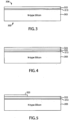
- FIG. 1 schematically shows a sectional view of a solar cell structure in accordance with an embodiment of the present invention.
- the solar cell is a backside contact solar cell in that its doped regions 101 and 102 are on the backside 106 opposite to the front side 105.
- the front side 105 faces the sun during normal operation.
- the doped regions 101 and 102 are formed on a thin dielectric layer 113.
- the dielectric layer 113 may be formed to a thickness of 5 Angstroms to 40 Angstroms.
- the dielectric layer 113 comprises silicon dioxide thermally grown on the surface of the substrate 103 to a thickness of 20 Angstroms.
- the dielectric layer 113 may also comprise silicon nitride.
- the dielectric layer 113 advantageously allows for surface passivation.
- the polysilicon of the doped regions 101 and 102 applies an electric field across the dielectric layer 113, which repels minority carriers and accumulates majority carriers at the dielectric interface.
- the doped region 101 is a P-type doped region, while the doped region 102 is an N-type doped region.
- a substrate 103 comprises an N-type silicon wafer in this example. As can be appreciated, the substrate 103 may also comprise a P-type silicon or other wafer with appropriate changes to the rest of the structure. There are several P-type and N-type doped regions in any given solar cell but only one of each is shown in FIG. 1 for clarity of illustration.
- the doped regions 101 and 102 may comprise doped polysilicon formed to a thickness of about 2000 Angstroms by low pressure chemical vapor deposition (LPCVD).
- the doped region 101 may comprise polysilicon doped with a P-type dopant (e.g., boron) and the doped region 102 may comprise polysilicon doped with an N-type dopant (e.g., phosphorus).
- the polysilicon may be deposited over the thin dielectric layer 113 and then doped by diffusion.
- the polysilicon may also be pre-doped prior to deposition on the dielectric layer 113.
- Polysilicon is the preferred material for the doped regions 101 and 102 for its compatibility with high temperature processing, allowing for increased thermal budget.
- the doped regions 101 and 102 are separated by a trench 104, which serves as a gap between the doped regions 101 and 102.
- the trench 104 may be formed by laser trenching or conventional etching, for example. In one embodiment, the trench 104 is about 100 microns wide.
- the trench 104 may be formed before or after a diffusion step that dopes the polysilicon doped regions 101 and 102. If the trench 104 is formed before the diffusion step, the passivation region 112 may comprise an N-type passivation region formed during the diffusion step.
- the trench 104 is formed using a process that not only forms the trench 104 but also forms a randomly textured surface 114 on the surface of the trench 104.
- the randomly textured surface 114 improves solar radiation collection of light incident on the back of the solar cell, i.e. a bifacial configuration.
- a wet etch process comprising potassium hydroxide and isopropyl alcohol may be used to form the trench 104 and to texture the surface 114 with random pyramids.
- the trench 104 may be formed to dig 1 to 10 microns (e.g., 3 microns) into the substrate 103.
- a dielectric in the form of a silicon nitride 107 is deposited in the trench 104.
- the silicon nitride 107 preferably has a relatively large positive fixed charge density to place the silicon surface under the trench 104 in accumulation and to provide good surface passivation.
- the positive fixed charge density of the silicon nitride 107 may naturally occur as part of the deposition process used to form the silicon nitride 107.
- the silicon nitride 107 is formed to a thickness of about 400 Angstroms by plasma enhanced chemical vapor deposition (PECVD).
- PECVD plasma enhanced chemical vapor deposition
- the resulting accumulation layer repels minority carriers, i.e. positively charged holes in N-type material.
- the trench 104 also prevents the space charge region from developing in the polysilicon.
- the space charge develops in the single crystal silicon underneath the P-type polysilicon. In this region, lifetime is not reduced due to grain boundaries, and hence the parasitic recombination is suppressed. A portion of this space charge region also intersects the surface of the wafer in the trench 104. The positive charge in the silicon nitride 107 reduces the impact of this region of space charge region as well narrowing the region.
- An example process flow for fabricating the solar cell structure of FIG. 1 may include forming a thin dielectric layer 113 over a backside surface of the substrate 103, forming an undoped polysilicon layer over the thin dielectric layer 113, doping the polysilicon layer into P-type and N-type doped regions 101 and 102, etching the doped polysilicon layer to form the trench 104 and the textured surface 114, forming the passivation region 112, and forming the silicon nitride 107 in the trench 104.
- the doped regions 101 and 102 may also be formed by depositing pre-doped polysilicon on the dielectric layer 113 using conventional deposition, masking, and etching techniques.
- the silicon nitride 107 preferably has a planar, as opposed to textured, surface.
- the planarity of the silicon nitride 107 is not critical and no additional planarization step is needed.
- the planarity of the silicon nitride 107 may be as deposited.
- the trench 104 may be formed before or after doping of the doped regions 101 and 102.
- interdigitated metal contact fingers 108 and 109 may be formed through the silicon nitride 107 to make an electrical connection to the doped regions 101 and 102, respectively. External electrical circuits may be attached to the interdigitated metal contact fingers 108 and 109 to connect to and be powered by the solar cell.
- the metal contact finger 108 may be connected to a positive electrical terminal and the metal contact finger 109 may be connected to a negative electrical terminal.
- the trench structure of FIG. 1 addresses the aforementioned issues relating to polysilicon parasitic space charge recombination several ways. Firstly, the trench 104 separates the doped regions 101 and 102 so they are not physically in contact. This prevents the space charge region from existing in either polysilicon film. Secondly, the resulting accumulation layer under the trench 104 repels minority carriers to improve surface passivation. Thirdly, the textured surface 114 in the trench 104 increases solar radiation collection. These advantageously help increase solar cell efficiency.
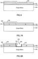
- FIGS. 3-10 show sectional views illustrating the fabrication of a solar cell in accordance with an embodiment of the present invention. There are a plurality of P-type doped regions and N-type doped regions in a solar cell but only one of each is shown as being fabricated in the following example for clarity of illustration.
- FIGS. 3-10 begins with formation of a thin dielectric layer 313 on a backside surface of a substrate 303 ( FIG. 3 ).
- the substrate 303 may comprise an N-type silicon wafer, for example.
- the dielectric layer 313 may be formed to a thickness of 5 Angstroms to 40 Angstroms (e.g., 20 Angstroms).
- the dielectric layer 313 comprises silicon dioxide thermally grown on the surface of the substrate 103.
- the dielectric layer 313 may also comprise silicon nitride, for example.
- An undoped polysilicon layer 322 is then formed on the dielectric layer 313.
- the polysilicon layer 322 may be formed to a thickness of about 2000 Angstroms by LPCVD, for example.
- a doped silicon dioxide layer 323 is then formed over the polysilicon layer 322 ( FIG. 4 ).
- the silicon dioxide layer 323 serves as a dopant source for a subsequently formed doped region, which is a P-type doped region 301 in this example (see FIG. 7A or 8B ).
- the silicon dioxide layer 323 may thus be doped with a P-type dopant, such as boron.
- the doped silicon dioxide layer 323 is patterned to remain over an area of the polysilicon layer 322 where the P-type doped region 301 is to be formed ( FIG. 5 ).
- the silicon dioxide layer 323 may be formed to a thickness of about 1000 Angstroms by APCVD.
- a doped silicon dioxide layer 324 is formed over the silicon dioxide 323 and the polysilicon layer 322 ( FIG. 6 ).
- the silicon dioxide 324 serves as a dopant source for a subsequently formed doped region, which is an N-type doped region 302 in this example (see FIG. 7A or 8B ).
- the silicon dioxide 324 may thus be doped with an N-type dopant, such as phosphorus.
- the silicon dioxide 324 may be formed to a thickness of about 2000 Angstroms by APCVD.
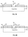
- the trench separating the doped regions may be formed before formation of the doped regions in a first trench formation process or after formation of the doped regions in a second trench formation process.
- FIGS. 7A and 8A illustrate process steps for the first trench formation process
- FIGS. 7B and 8B illustrate process steps for the second trench formation process. Both trench formation processes may proceed from FIG. 6 and continue on to FIG. 9 .
- a thermal drive-in step diffuses dopants from the silicon dioxides 323 and 324 to the underlying polysilicon layer 322, thereby forming P-type and N-type doped regions in the polysilicon layer 322, which is accordingly relabeled as P-type doped region 301 and N-type doped region 302 ( FIG. 7A ).
- the thermal drive-in step may be performed by heating the sample of FIG. 6 .
- the preferred drive conditions give a heavily doped, e.g., greater than 1e 20 cm -3 , polysilicon layer that is uniform throughout the thickness of the film and has very little doping under the polysilicon, e.g., equal to or less than 1e 18 cm -3 .
- the thermal drive-in step results in the polysilicon layer 322 under the silicon dioxide 323 forming the P-type doped region 301 and polysilicon layer 322 under the silicon dioxide 324 forming the N-type doped region 302.
- the silicon dioxide 324, silicon dioxide 323, doped region 301, doped region 302, and thin dielectric layer 313 are etched to form a trench 304 ( FIG. 8A ).
- the trench etch may comprise a multi-step etch process, with the last etch step stopping on the substrate 303.
- the trench 304 may be about 100 microns wide, for example. However, there is no known limit to the minimum width as long as the P-type doped region 301 and N-type doped region 302 do not contact each other.
- the trench 304 may be formed by conventional etching processes including by laser trenching. In one embodiment, the trench 304 has a textured surface 314 for improved solar radiation collection efficiency.
- a wet etch process comprising potassium hydroxide and isopropyl alcohol is used to form the trench 304 and to texture the surface 314 with random pyramids.
- the trench 304 may extend 1 to 10 microns, e.g., 3 microns, into the substrate 303.
- a thin (less than 200 Angstroms, e.g., 100 Angstroms) passivation layer 310 is formed on the surface 314 of the trench 304.
- the passivation layer 310 may comprise silicon dioxide thermally grown on the surface 314 or deposited silicon nitride layer, for example.
- the silicon dioxide 324, silicon dioxide 322, and thin dielectric layer 313 of the sample of FIG. 6 are etched to form the trench 304 ( FIG. 7B ).
- Textured surface 314 may be formed on the surface of the trench 304.
- the trench etch is essentially the same as in the first trench formation process except that the trench is formed before formation of the doped regions of the solar cell.
- a thermal drive-in step is performed to diffuse dopants from the silicon dioxide layers 323 and 324 to the underlying polysilicon layer 322, thereby forming the doped regions 301 and 302 as in the first trench formation process ( FIG. 8B ).
- a passivation region 315 is formed in the substrate 303 under the trench 304 during the diffusion process.
- the passivation region 315 may comprise diffused N-type dopants.
- the passivation region 315 is formed by introducing POCI3 (phosphorus chloride oxide) in the diffusion furnace during the thermal drive-in.
- the passivation region 315 serves the same function as the passivation region 112 of FIG. 1 .
- the trench 304 serves as a gap physically separating the P-type doped region 301 from the N-type doped region 302.
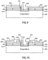
- the processing of the solar cell continues from either FIG. 8A or 8B to FIG. 9 .
- a dielectric in the form of a silicon nitride layer 307 is formed in the trench 304.
- the silicon nitride layer 307 is also formed over the layers 323 and 324.
- the silicon nitride layer 307 preferably has a relatively large positive fixed charge density to place the silicon surface under the trench 304 in accumulation and to provide good surface passivation.
- the positive fixed charge density on the silicon nitride layer 307 may naturally occur as part of a PECVD process, for example.
- the silicon nitride 307 is formed to a thickness of about 400 Angstroms by PECVD.
- the silicon nitride 307 preferably has a planar (e.g., as deposited) surface.
- the passivation region 312 represents either the passivation layer 310 (see FIG. 8A ) or the passivation region 315 (see FIG. 8B ) depending on the trench formation process used.
- Interdigitated metal contact fingers 308 and 309 may then be formed through the silicon nitride 307 to make an electrical connection to the doped regions 301 and 302 by way of layers 323 and 324, respectively ( FIG. 10 ). External electrical circuits may be attached to the interdigitated metal contact fingers 308 and 309 to connect to and be powered by the solar cell.
- the metal contact finger 308 may be coupled to a positive electrical terminal and the metal contact finger 309 may be coupled to a negative electrical terminal.
- the resulting solar cell provides the same benefits as the solar cell of FIG. 1 .
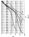
- FIG. 11 shows dark I-V (i.e., current-voltage) curves comparing the performance of a conventional solar cell to a solar cell that is in accordance with an embodiment of the present invention.
- the I-V curves are "dark" in that they were measured with no direct solar radiation shining on the solar cells.
- the I-V curves are for the diodes formed between an N-type silicon and a P-type doped region.
- the horizontal axis represents voltage across the diode and the vertical axis represents the resulting current across the diode.
- Plot 401 is the I-V curve for a conventional solar cell with touching P-type and N-type polysilicon doped regions
- plot 402 is the I-V curve for a typical Sunpower Corporation A300 TM solar cell
- plot 403 is for a solar cell having a trench between the P-type and N-type doped regions as in FIGS. 1 and 9 . While the plot 402 is very close to the ideal I-V curve represented by the plot 404, the plot 403 is even closer.
- the plot 405 represents a guide for the eye of an ideal diode I-V characteristic, the slope of which is 60 millivolts per decade of current.
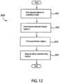
- doped regions are formed in a polysilicon layer (step 601).
- the doped regions may be formed by depositing doped silicon dioxide layers over an undoped polysilicon layer and performing a diffusion step, by depositing pre-doped silicon dioxide layers, or by depositing an undoped polysilicon layer followed by a dopant implantation step, for example.
- the polysilicon layer where the doped regions are formed may be etched to form a trench separating the P-type doped region from the N-type doped region (step 602). Alternatively, the trench is formed before the doped regions are formed.
- the trench may include a textured surface for increased solar radiation collection.
- a passivation region such as passivation layer or a diffused region in the substrate, may be formed to isolate trench material from the bulk of the substrate (step 603).
- a dielectric in the form of a silicon nitride layer may then be deposited in the trench (step 604). Interdigitated metal contact fingers may thereafter be formed to electrically connect to the P-type and N-type doped regions through the silicon nitride.
Landscapes
- Engineering & Computer Science (AREA)
- Life Sciences & Earth Sciences (AREA)
- Sustainable Energy (AREA)
- Photovoltaic Devices (AREA)
- Sustainable Development (AREA)
- Chemical & Material Sciences (AREA)
- Crystallography & Structural Chemistry (AREA)
- Manufacturing & Machinery (AREA)
Priority Applications (1)
| Application Number | Priority Date | Filing Date | Title |
|---|---|---|---|
| EP24162582.1A EP4358155A3 (en) | 2008-06-12 | 2009-04-29 | Trench process and structure for backside contact solar cells with polysilicon doped regions |
Applications Claiming Priority (4)
| Application Number | Priority Date | Filing Date | Title |
|---|---|---|---|
| US6092108P | 2008-06-12 | 2008-06-12 | |
| US12/431,684 US7812250B2 (en) | 2008-06-12 | 2009-04-28 | Trench process and structure for backside contact solar cells with polysilicon doped regions |
| PCT/US2009/042130 WO2009151808A1 (en) | 2008-06-12 | 2009-04-29 | Trench process and structure for backside contact solar cells with polysilicon doped regions |
| EP09763099.0A EP2297788B1 (en) | 2008-06-12 | 2009-04-29 | Back-contacted solar cells with doped polysilicon regions separated via trench structures and fabrication process therefor |
Related Parent Applications (2)
| Application Number | Title | Priority Date | Filing Date |
|---|---|---|---|
| EP09763099.0A Division-Into EP2297788B1 (en) | 2008-06-12 | 2009-04-29 | Back-contacted solar cells with doped polysilicon regions separated via trench structures and fabrication process therefor |
| EP09763099.0A Division EP2297788B1 (en) | 2008-06-12 | 2009-04-29 | Back-contacted solar cells with doped polysilicon regions separated via trench structures and fabrication process therefor |
Related Child Applications (1)
| Application Number | Title | Priority Date | Filing Date |
|---|---|---|---|
| EP24162582.1A Division EP4358155A3 (en) | 2008-06-12 | 2009-04-29 | Trench process and structure for backside contact solar cells with polysilicon doped regions |
Publications (3)
| Publication Number | Publication Date |
|---|---|
| EP3065184A1 EP3065184A1 (en) | 2016-09-07 |
| EP3065184C0 EP3065184C0 (en) | 2024-03-13 |
| EP3065184B1 true EP3065184B1 (en) | 2024-03-13 |
Family
ID=41413646
Family Applications (4)
| Application Number | Title | Priority Date | Filing Date |
|---|---|---|---|
| EP16165135.1A Active EP3065184B1 (en) | 2008-06-12 | 2009-04-29 | Trench process and structure for backside contact solar cells with polysilicon doped regions |
| EP09763099.0A Active EP2297788B1 (en) | 2008-06-12 | 2009-04-29 | Back-contacted solar cells with doped polysilicon regions separated via trench structures and fabrication process therefor |
| EP24162582.1A Pending EP4358155A3 (en) | 2008-06-12 | 2009-04-29 | Trench process and structure for backside contact solar cells with polysilicon doped regions |
| EP09763100.6A Active EP2297789B1 (en) | 2008-06-12 | 2009-04-29 | Trench process and structure for backside contact solar cells with polysilicon doped regions |
Family Applications After (3)
| Application Number | Title | Priority Date | Filing Date |
|---|---|---|---|
| EP09763099.0A Active EP2297788B1 (en) | 2008-06-12 | 2009-04-29 | Back-contacted solar cells with doped polysilicon regions separated via trench structures and fabrication process therefor |
| EP24162582.1A Pending EP4358155A3 (en) | 2008-06-12 | 2009-04-29 | Trench process and structure for backside contact solar cells with polysilicon doped regions |
| EP09763100.6A Active EP2297789B1 (en) | 2008-06-12 | 2009-04-29 | Trench process and structure for backside contact solar cells with polysilicon doped regions |
Country Status (10)
| Country | Link |
|---|---|
| US (15) | US7851698B2 (enExample) |
| EP (4) | EP3065184B1 (enExample) |
| JP (5) | JP5524194B2 (enExample) |
| KR (2) | KR101466753B1 (enExample) |
| CN (4) | CN102057497B (enExample) |
| AU (2) | AU2009257973B2 (enExample) |
| ES (1) | ES2979023T3 (enExample) |
| MY (2) | MY177509A (enExample) |
| PL (1) | PL3065184T3 (enExample) |
| WO (2) | WO2009151809A1 (enExample) |
Families Citing this family (166)
| Publication number | Priority date | Publication date | Assignee | Title |
|---|---|---|---|---|
| US7442629B2 (en) | 2004-09-24 | 2008-10-28 | President & Fellows Of Harvard College | Femtosecond laser-induced formation of submicrometer spikes on a semiconductor substrate |
| US7057256B2 (en) | 2001-05-25 | 2006-06-06 | President & Fellows Of Harvard College | Silicon-based visible and near-infrared optoelectric devices |
| US8614395B1 (en) | 2007-11-01 | 2013-12-24 | Sandia Corporation | Solar cell with back side contacts |
| KR100974221B1 (ko) * | 2008-04-17 | 2010-08-06 | 엘지전자 주식회사 | 레이저 어닐링을 이용한 태양전지의 선택적 에미터형성방법 및 이를 이용한 태양전지의 제조방법 |
| US12074240B2 (en) * | 2008-06-12 | 2024-08-27 | Maxeon Solar Pte. Ltd. | Backside contact solar cells with separated polysilicon doped regions |
| US7851698B2 (en) * | 2008-06-12 | 2010-12-14 | Sunpower Corporation | Trench process and structure for backside contact solar cells with polysilicon doped regions |
| US8242354B2 (en) * | 2008-12-04 | 2012-08-14 | Sunpower Corporation | Backside contact solar cell with formed polysilicon doped regions |
| KR101539047B1 (ko) * | 2008-12-24 | 2015-07-23 | 인텔렉츄얼 키스톤 테크놀로지 엘엘씨 | 광기전력 변환 소자 및 그의 제조방법 |
| US9064999B2 (en) | 2009-09-07 | 2015-06-23 | Lg Electronics Inc. | Solar cell and method for manufacturing the same |
| US9673243B2 (en) | 2009-09-17 | 2017-06-06 | Sionyx, Llc | Photosensitive imaging devices and associated methods |
| US9911781B2 (en) * | 2009-09-17 | 2018-03-06 | Sionyx, Llc | Photosensitive imaging devices and associated methods |
| US8603900B2 (en) * | 2009-10-27 | 2013-12-10 | Varian Semiconductor Equipment Associates, Inc. | Reducing surface recombination and enhancing light trapping in solar cells |
| US8324015B2 (en) * | 2009-12-01 | 2012-12-04 | Sunpower Corporation | Solar cell contact formation using laser ablation |
| WO2011072179A2 (en) | 2009-12-09 | 2011-06-16 | Solexel, Inc. | High-efficiency photovoltaic back-contact solar cell structures and manufacturing methods using semiconductor wafers |
| JP5845445B2 (ja) * | 2010-01-26 | 2016-01-20 | パナソニックIpマネジメント株式会社 | 太陽電池及びその製造方法 |
| US8790957B2 (en) * | 2010-03-04 | 2014-07-29 | Sunpower Corporation | Method of fabricating a back-contact solar cell and device thereof |
| US8692198B2 (en) | 2010-04-21 | 2014-04-08 | Sionyx, Inc. | Photosensitive imaging devices and associated methods |
| US8211731B2 (en) | 2010-06-07 | 2012-07-03 | Sunpower Corporation | Ablation of film stacks in solar cell fabrication processes |
| EP2395554A3 (en) | 2010-06-14 | 2015-03-11 | Imec | Fabrication method for interdigitated back contact photovoltaic cells |
| US20120146172A1 (en) | 2010-06-18 | 2012-06-14 | Sionyx, Inc. | High Speed Photosensitive Devices and Associated Methods |
| US8263899B2 (en) | 2010-07-01 | 2012-09-11 | Sunpower Corporation | High throughput solar cell ablation system |
| US8377738B2 (en) * | 2010-07-01 | 2013-02-19 | Sunpower Corporation | Fabrication of solar cells with counter doping prevention |
| EP2601687A4 (en) | 2010-08-05 | 2018-03-07 | Solexel, Inc. | Backplane reinforcement and interconnects for solar cells |
| US20120048372A1 (en) * | 2010-08-25 | 2012-03-01 | Hyungseok Kim | Solar cell |
| US8492253B2 (en) * | 2010-12-02 | 2013-07-23 | Sunpower Corporation | Method of forming contacts for a back-contact solar cell |
| US8134217B2 (en) * | 2010-12-14 | 2012-03-13 | Sunpower Corporation | Bypass diode for a solar cell |
| US8586403B2 (en) | 2011-02-15 | 2013-11-19 | Sunpower Corporation | Process and structures for fabrication of solar cells with laser ablation steps to form contact holes |
| US8129215B1 (en) | 2011-04-01 | 2012-03-06 | James P Campbell | Method for producing high temperature thin film silicon layer on glass |
| US8802486B2 (en) | 2011-04-25 | 2014-08-12 | Sunpower Corporation | Method of forming emitters for a back-contact solar cell |
| KR101724005B1 (ko) * | 2011-04-29 | 2017-04-07 | 삼성에스디아이 주식회사 | 태양전지와 그 제조 방법 |
| US9496308B2 (en) | 2011-06-09 | 2016-11-15 | Sionyx, Llc | Process module for increasing the response of backside illuminated photosensitive imagers and associated methods |
| US8658458B2 (en) | 2011-06-15 | 2014-02-25 | Varian Semiconductor Equipment Associates, Inc. | Patterned doping for polysilicon emitter solar cells |
| US20130016203A1 (en) | 2011-07-13 | 2013-01-17 | Saylor Stephen D | Biometric imaging devices and associated methods |
| US8692111B2 (en) | 2011-08-23 | 2014-04-08 | Sunpower Corporation | High throughput laser ablation processes and structures for forming contact holes in solar cells |
| US8586397B2 (en) * | 2011-09-30 | 2013-11-19 | Sunpower Corporation | Method for forming diffusion regions in a silicon substrate |
| US8889981B2 (en) * | 2011-10-18 | 2014-11-18 | Samsung Sdi Co., Ltd. | Photoelectric device |
| KR20130050721A (ko) | 2011-11-08 | 2013-05-16 | 삼성에스디아이 주식회사 | 태양 전지 |
| CN102508577A (zh) * | 2011-11-21 | 2012-06-20 | 苏州盖娅智能科技有限公司 | 太阳能触感式控制面板 |
| KR101757874B1 (ko) | 2011-12-08 | 2017-07-14 | 엘지전자 주식회사 | 태양 전지 |
| US20130146136A1 (en) * | 2011-12-13 | 2013-06-13 | Kyoung-Jin Seo | Photovoltaic device and method of manufacturing the same |
| AU2012358982B2 (en) * | 2011-12-21 | 2015-05-07 | Maxeon Solar Pte. Ltd. | Hybrid polysilicon heterojunction back contact cell |
| US8822262B2 (en) | 2011-12-22 | 2014-09-02 | Sunpower Corporation | Fabricating solar cells with silicon nanoparticles |
| US8513045B1 (en) | 2012-01-31 | 2013-08-20 | Sunpower Corporation | Laser system with multiple laser pulses for fabrication of solar cells |
| US9064764B2 (en) | 2012-03-22 | 2015-06-23 | Sionyx, Inc. | Pixel isolation elements, devices, and associated methods |
| US9054255B2 (en) | 2012-03-23 | 2015-06-09 | Sunpower Corporation | Solar cell having an emitter region with wide bandgap semiconductor material |
| DE102012205378A1 (de) * | 2012-04-02 | 2013-10-02 | Robert Bosch Gmbh | Verfahren zur Herstellung von Dünnschichtsolarmodulen sowie nach diesem Verfahren erhältliche Dünnschichtsolarmodule |
| WO2013163231A1 (en) * | 2012-04-23 | 2013-10-31 | Solexel, Inc. | Resistance component extraction for back contact back junction solar cells |
| US10453120B2 (en) * | 2012-04-27 | 2019-10-22 | Advanced Promotional Technologies, Inc. | Networked computer system and computer implemented methods for providing an online auction webpage with skill-based game |
| NL2008755C2 (en) * | 2012-05-04 | 2013-11-06 | Tempress Ip B V | Method of manufacturing a solar cell and equipment therefore. |
| KR101977927B1 (ko) * | 2012-07-11 | 2019-05-13 | 인텔렉츄얼 키스톤 테크놀로지 엘엘씨 | 광전소자 및 그 제조방법 |
| US10014425B2 (en) * | 2012-09-28 | 2018-07-03 | Sunpower Corporation | Spacer formation in a solar cell using oxygen ion implantation |
| CN104813480B (zh) | 2012-10-16 | 2017-03-01 | 索莱克赛尔公司 | 用于光伏太阳能电池和模块中的单片集成旁路开关的系统和方法 |
| US9812590B2 (en) * | 2012-10-25 | 2017-11-07 | Sunpower Corporation | Bifacial solar cell module with backside reflector |
| US9515217B2 (en) | 2012-11-05 | 2016-12-06 | Solexel, Inc. | Monolithically isled back contact back junction solar cells |
| WO2014071417A2 (en) * | 2012-11-05 | 2014-05-08 | Solexel, Inc. | Systems and methods for monolithically isled solar photovoltaic cells and modules |
| US20140130854A1 (en) * | 2012-11-12 | 2014-05-15 | Samsung Sdi Co., Ltd. | Photoelectric device and the manufacturing method thereof |
| US9472702B1 (en) | 2012-11-19 | 2016-10-18 | Sandia Corporation | Photovoltaic cell with nano-patterned substrate |
| US9018516B2 (en) * | 2012-12-19 | 2015-04-28 | Sunpower Corporation | Solar cell with silicon oxynitride dielectric layer |
| WO2014127067A1 (en) * | 2013-02-12 | 2014-08-21 | Solexel, Inc. | Monolithically isled back contact back junction solar cells using bulk wafers |
| JP6466346B2 (ja) | 2013-02-15 | 2019-02-06 | サイオニクス、エルエルシー | アンチブルーミング特性を有するハイダイナミックレンジcmos画像センサおよび関連づけられた方法 |
| WO2014151093A1 (en) | 2013-03-15 | 2014-09-25 | Sionyx, Inc. | Three dimensional imaging utilizing stacked imager devices and associated methods |
| EP4092757A1 (en) | 2013-04-03 | 2022-11-23 | Lg Electronics Inc. | Method for fabricating a solar cell |
| KR101613843B1 (ko) | 2013-04-23 | 2016-04-20 | 엘지전자 주식회사 | 태양 전지 및 이의 제조 방법 |
| KR102045001B1 (ko) * | 2013-06-05 | 2019-12-02 | 엘지전자 주식회사 | 태양 전지 및 이의 제조 방법 |
| US9209345B2 (en) | 2013-06-29 | 2015-12-08 | Sionyx, Inc. | Shallow trench textured regions and associated methods |
| KR101622089B1 (ko) | 2013-07-05 | 2016-05-18 | 엘지전자 주식회사 | 태양 전지 및 이의 제조 방법 |
| US20150090328A1 (en) * | 2013-09-27 | 2015-04-02 | Sunpower Corporation | Epitaxial silicon solar cells with moisture barrier |
| DE102013219565A1 (de) | 2013-09-27 | 2015-04-02 | Fraunhofer-Gesellschaft zur Förderung der angewandten Forschung e.V. | Photovoltaische Solarzelle und Verfahren zum Herstellen einer photovoltaischen Solarzelle |
| DE102013219561A1 (de) | 2013-09-27 | 2015-04-02 | Fraunhofer-Gesellschaft zur Förderung der angewandten Forschung e.V. | Verfahren zum Herstellen einer photovoltaischen Solarzelle mit zumindest einem Heteroübergang |
| DE102013219564A1 (de) * | 2013-09-27 | 2015-04-02 | Fraunhofer-Gesellschaft zur Förderung der angewandten Forschung e.V. | Verfahren zum Herstellen einer photovoltaischen Solarzelle mit einem Heteroübergang |
| US9437756B2 (en) * | 2013-09-27 | 2016-09-06 | Sunpower Corporation | Metallization of solar cells using metal foils |
| KR102085828B1 (ko) * | 2013-10-29 | 2020-03-06 | 엘지전자 주식회사 | 태양 전지 및 이의 제조 방법 |
| US9577134B2 (en) * | 2013-12-09 | 2017-02-21 | Sunpower Corporation | Solar cell emitter region fabrication using self-aligned implant and cap |
| US9401450B2 (en) | 2013-12-09 | 2016-07-26 | Sunpower Corporation | Solar cell emitter region fabrication using ion implantation |
| US9196758B2 (en) * | 2013-12-20 | 2015-11-24 | Sunpower Corporation | Solar cell emitter region fabrication with differentiated p-type and n-type region architectures |
| US20150179847A1 (en) | 2013-12-20 | 2015-06-25 | Seung Bum Rim | Built-in bypass diode |
| KR102173644B1 (ko) * | 2014-01-29 | 2020-11-03 | 엘지전자 주식회사 | 태양 전지 및 이의 제조 방법 |
| KR102246280B1 (ko) * | 2014-03-26 | 2021-04-29 | 에스케이하이닉스 주식회사 | 반도체 소자 및 그 제조 방법 |
| US20150280043A1 (en) * | 2014-03-27 | 2015-10-01 | David D. Smith | Solar cell with trench-free emitter regions |
| US9337369B2 (en) * | 2014-03-28 | 2016-05-10 | Sunpower Corporation | Solar cells with tunnel dielectrics |
| KR101569417B1 (ko) * | 2014-07-07 | 2015-11-16 | 엘지전자 주식회사 | 태양 전지 |
| US9837259B2 (en) | 2014-08-29 | 2017-12-05 | Sunpower Corporation | Sequential etching treatment for solar cell fabrication |
| US9837576B2 (en) * | 2014-09-19 | 2017-12-05 | Sunpower Corporation | Solar cell emitter region fabrication with differentiated P-type and N-type architectures and incorporating dotted diffusion |
| DE102014218948A1 (de) | 2014-09-19 | 2016-03-24 | Fraunhofer-Gesellschaft zur Förderung der angewandten Forschung e.V. | Solarzelle mit einer amorphen Siliziumschicht und Verfahren zum Herstellen solch einer photovoltaischen Solarzelle |
| US9246046B1 (en) * | 2014-09-26 | 2016-01-26 | Sunpower Corporation | Etching processes for solar cell fabrication |
| KR102219804B1 (ko) * | 2014-11-04 | 2021-02-24 | 엘지전자 주식회사 | 태양 전지 및 그의 제조 방법 |
| JP6219913B2 (ja) | 2014-11-28 | 2017-10-25 | エルジー エレクトロニクス インコーポレイティド | 太陽電池及びその製造方法 |
| US20160163901A1 (en) * | 2014-12-08 | 2016-06-09 | Benjamin Ian Hsia | Laser stop layer for foil-based metallization of solar cells |
| US9997652B2 (en) * | 2015-03-23 | 2018-06-12 | Sunpower Corporation | Deposition approaches for emitter layers of solar cells |
| US9559245B2 (en) * | 2015-03-23 | 2017-01-31 | Sunpower Corporation | Blister-free polycrystalline silicon for solar cells |
| US9525083B2 (en) | 2015-03-27 | 2016-12-20 | Sunpower Corporation | Solar cell emitter region fabrication with differentiated P-type and N-type architectures and incorporating a multi-purpose passivation and contact layer |
| US11355657B2 (en) | 2015-03-27 | 2022-06-07 | Sunpower Corporation | Metallization of solar cells with differentiated p-type and n-type region architectures |
| US20160284917A1 (en) * | 2015-03-27 | 2016-09-29 | Seung Bum Rim | Passivation Layer for Solar Cells |
| DE102015107842B3 (de) | 2015-05-19 | 2016-10-27 | Institut Für Solarenergieforschung Gmbh | Verfahren zum Herstellen einer Solarzelle mit oxidierten Zwischenbereichen zwischen Poly-Silizium-Kontakten |
| KR102272433B1 (ko) * | 2015-06-30 | 2021-07-05 | 엘지전자 주식회사 | 태양 전지 및 이의 제조 방법 |
| DE102015015017A1 (de) | 2015-11-19 | 2017-05-24 | Institut Für Solarenergieforschung Gmbh | Solarzelle und Verfahren zur Herstellung einer Solarzelle mit mehreren durch ladungsträgerselektive Kontakte miteinander verbundenen Absorbern |
| US10079319B2 (en) * | 2015-12-16 | 2018-09-18 | Sunpower Corporation | Solar cell fabrication using laser patterning of ion-implanted etch-resistant layers and the resulting solar cells |
| KR102600379B1 (ko) * | 2015-12-21 | 2023-11-10 | 상라오 징코 솔라 테크놀러지 디벨롭먼트 컴퍼니, 리미티드 | 태양 전지와 그 제조 방법 |
| WO2017111697A1 (en) * | 2015-12-24 | 2017-06-29 | Trina Solar Energy Development Pte Ltd. | A method of fabricating a heterojunction all-back-contact solar cell |
| JP6619273B2 (ja) * | 2016-03-23 | 2019-12-11 | シャープ株式会社 | 光電変換装置 |
| US10217880B2 (en) * | 2016-03-30 | 2019-02-26 | Sunpower Corporation | Voltage breakdown device for solar cells |
| JP6133465B2 (ja) * | 2016-04-01 | 2017-05-24 | シャープ株式会社 | 光電変換装置およびその製造方法 |
| US9502601B1 (en) * | 2016-04-01 | 2016-11-22 | Sunpower Corporation | Metallization of solar cells with differentiated P-type and N-type region architectures |
| USD822890S1 (en) | 2016-09-07 | 2018-07-10 | Felxtronics Ap, Llc | Lighting apparatus |
| US10147829B2 (en) | 2016-09-23 | 2018-12-04 | Taiwan Semiconductor Manufacturing Co., Ltd. | Dielectric sidewall structure for quality improvement in Ge and SiGe devices |
| US10775030B2 (en) | 2017-05-05 | 2020-09-15 | Flex Ltd. | Light fixture device including rotatable light modules |
| USD862777S1 (en) | 2017-08-09 | 2019-10-08 | Flex Ltd. | Lighting module wide distribution lens |
| USD877964S1 (en) | 2017-08-09 | 2020-03-10 | Flex Ltd. | Lighting module |
| USD846793S1 (en) | 2017-08-09 | 2019-04-23 | Flex Ltd. | Lighting module locking mechanism |
| USD833061S1 (en) | 2017-08-09 | 2018-11-06 | Flex Ltd. | Lighting module locking endcap |
| USD832494S1 (en) | 2017-08-09 | 2018-10-30 | Flex Ltd. | Lighting module heatsink |
| USD872319S1 (en) | 2017-08-09 | 2020-01-07 | Flex Ltd. | Lighting module LED light board |
| USD832495S1 (en) | 2017-08-18 | 2018-10-30 | Flex Ltd. | Lighting module locking mechanism |
| USD862778S1 (en) | 2017-08-22 | 2019-10-08 | Flex Ltd | Lighting module lens |
| USD888323S1 (en) | 2017-09-07 | 2020-06-23 | Flex Ltd | Lighting module wire guard |
| CN107775285B (zh) * | 2017-09-08 | 2019-11-22 | 西安理工大学 | 一种提高砂芯造型机导轨耐磨性的表面织构化方法 |
| US20190207041A1 (en) * | 2017-12-29 | 2019-07-04 | Sunpower Corporation | Solar cells having differentiated p-type and n-type architectures fabricated using an etch paste |
| JP2021520056A (ja) | 2018-04-16 | 2021-08-12 | サンパワー コーポレイション | クリーブ加工された縁部から後退した接合部を有する太陽電池 |
| US11682744B2 (en) * | 2018-09-28 | 2023-06-20 | Maxeon Solar Pte. Ltd. | Solar cells having hybrid architectures including differentiated P-type and N-type regions |
| US20240274734A1 (en) * | 2018-12-27 | 2024-08-15 | Solarpaint Ltd. | Flexible Solar Panels and Photovoltaic Devices, and Methods and Systems for Producing Them |
| CN109713065B (zh) * | 2018-12-28 | 2023-10-31 | 泰州中来光电科技有限公司 | 一种印刷金属电极的钝化太阳能电池及其制备方法 |
| CN110299417A (zh) * | 2019-06-05 | 2019-10-01 | 国家电投集团西安太阳能电力有限公司 | 一种双面ibc电池结构及其制备方法 |
| US10777611B1 (en) * | 2019-09-27 | 2020-09-15 | Sony Semiconductor Solutions Corporation | Image sensor |
| JP7539407B2 (ja) * | 2019-11-27 | 2024-08-23 | 株式会社カネカ | 太陽電池の製造方法 |
| US11824126B2 (en) * | 2019-12-10 | 2023-11-21 | Maxeon Solar Pte. Ltd. | Aligned metallization for solar cells |
| CN111180544B (zh) * | 2020-01-06 | 2021-09-10 | 浙江晶科能源有限公司 | 一种钝化接触晶体硅太阳能电池及其制作方法 |
| CN111276569B (zh) * | 2020-02-17 | 2022-10-11 | 浙江爱旭太阳能科技有限公司 | 一种增强perc背钝化效果的电池制作方法 |
| EP3982421A1 (en) | 2020-10-09 | 2022-04-13 | International Solar Energy Research Center Konstanz E.V. | Method for local modification of etching resistance in a silicon layer, use of this method in the production of passivating contact solar cells and thus-created solar cell |
| CN113299771B (zh) * | 2021-06-04 | 2025-10-21 | 浙江爱旭太阳能科技有限公司 | 一种选择性接触区域掩埋型太阳能电池及其背面接触结构 |
| CN113299770A (zh) | 2021-06-04 | 2021-08-24 | 浙江爱旭太阳能科技有限公司 | 一种选择性接触区域掩埋型太阳能电池及其背面接触结构 |
| CN121078843A (zh) | 2021-06-04 | 2025-12-05 | 浙江爱旭太阳能科技有限公司 | 一种选择性接触区域掩埋型太阳能电池及其背面接触结构 |
| US12009440B2 (en) * | 2021-07-22 | 2024-06-11 | Solarlab Aiko Europe Gmbh | Doped region structure and solar cell comprising the same, cell assembly, and photovoltaic system |
| CN113964216B (zh) * | 2021-09-22 | 2023-10-27 | 泰州隆基乐叶光伏科技有限公司 | 一种背接触电池及其制作方法 |
| CN113921625B (zh) * | 2021-09-30 | 2023-10-27 | 泰州隆基乐叶光伏科技有限公司 | 一种背接触电池及其制作方法 |
| CN113921626A (zh) * | 2021-09-30 | 2022-01-11 | 泰州隆基乐叶光伏科技有限公司 | 一种背接触电池的制作方法 |
| EP4195299A1 (en) | 2021-12-13 | 2023-06-14 | International Solar Energy Research Center Konstanz E.V. | Interdigitated back contact solar cell and method for producing an interdigitated back contact solar cell |
| CN116417522A (zh) * | 2021-12-29 | 2023-07-11 | 泰州隆基乐叶光伏科技有限公司 | 一种太阳能电池及其制备方法 |
| CN114744055B (zh) * | 2022-03-11 | 2024-03-29 | 浙江爱旭太阳能科技有限公司 | 一种太阳能电池及其接触结构、电池组件和光伏系统 |
| CN116741849A (zh) * | 2022-06-08 | 2023-09-12 | 浙江晶科能源有限公司 | 一种太阳能电池及光伏组件 |
| CN116741850A (zh) * | 2022-06-08 | 2023-09-12 | 浙江晶科能源有限公司 | 一种太阳能电池及光伏组件 |
| DE102022116798A1 (de) | 2022-07-06 | 2024-01-11 | EnPV GmbH | Rückseitenkontaktierte Solarzelle mit passivierten Kontakten und Herstellungsverfahren |
| CN115566088B (zh) * | 2022-08-22 | 2025-08-12 | 泰州隆基乐叶光伏科技有限公司 | 一种背接触电池及其制造方法、光伏组件 |
| CN115548144B (zh) * | 2022-11-04 | 2024-05-07 | 安徽华晟新能源科技有限公司 | 半导体衬底及其处理方法、太阳能电池及其制备方法 |
| CN118198165A (zh) * | 2022-12-07 | 2024-06-14 | 浙江晶科能源有限公司 | 太阳能电池及其制备方法、光伏组件 |
| CN116314415B (zh) * | 2023-02-10 | 2024-09-27 | 天合光能股份有限公司 | 背接触太阳能电池和制备方法 |
| CN116093190B (zh) * | 2023-02-10 | 2024-09-20 | 天合光能股份有限公司 | 背接触太阳能电池及其制备方法 |
| CN120547982A (zh) * | 2023-03-31 | 2025-08-26 | 天合光能股份有限公司 | 太阳电池及太阳电池的制备方法 |
| WO2024228665A1 (en) * | 2023-04-30 | 2024-11-07 | Maxeon Solar Pte. Ltd. | Solar cell with cell architecture designed for reduced carrier recombination |
| CN116230783B (zh) * | 2023-05-09 | 2023-10-03 | 天合光能股份有限公司 | 太阳能电池、太阳能电池片和光伏组件 |
| CN119008711A (zh) * | 2023-10-13 | 2024-11-22 | 浙江晶科能源有限公司 | 太阳能电池及其制备方法、光伏组件 |
| CN119008712A (zh) | 2023-10-13 | 2024-11-22 | 浙江晶科能源有限公司 | 太阳能电池及光伏组件 |
| CN117334760B (zh) * | 2023-10-25 | 2024-08-20 | 天合光能股份有限公司 | 一种全背接触电池结构及其制备方法 |
| CN117497626B (zh) * | 2023-12-14 | 2024-04-23 | 天合光能股份有限公司 | 太阳能电池和太阳能电池的制造方法 |
| CN117423762B (zh) * | 2023-12-15 | 2024-09-03 | 天合光能股份有限公司 | 太阳电池及其制备方法、光伏组件、光伏系统 |
| CN118053927A (zh) | 2023-12-15 | 2024-05-17 | 浙江晶科能源有限公司 | 太阳能电池及其制备方法、光伏组件 |
| CN118053928A (zh) | 2023-12-15 | 2024-05-17 | 浙江晶科能源有限公司 | 太阳能电池及光伏组件 |
| CN118053922A (zh) * | 2023-12-15 | 2024-05-17 | 浙江晶科能源有限公司 | 太阳能电池及其制备方法、光伏组件 |
| CN117712229B (zh) * | 2023-12-28 | 2024-10-01 | 江苏凌众新能科技有限公司 | 一种高效n型背接触太阳能电池制备工艺 |
| CN117810276A (zh) * | 2024-03-01 | 2024-04-02 | 隆基绿能科技股份有限公司 | 一种背接触电池及其制造方法 |
| CN118198191B (zh) * | 2024-03-21 | 2025-11-14 | 天合光能股份有限公司 | 背接触太阳能电池的制备方法及背接触太阳能电池 |
| CN118016740B (zh) * | 2024-04-02 | 2024-09-13 | 浙江晶科能源有限公司 | 太阳能电池及其制备方法、光伏组件 |
| CN118431349B (zh) * | 2024-04-26 | 2025-06-13 | 天合光能股份有限公司 | 背接触异质结电池的制备方法 |
| CN118156342B (zh) * | 2024-05-10 | 2024-08-20 | 金阳(泉州)新能源科技有限公司 | 一种具有耐酸绝缘隔离区的背接触电池及其制作和应用 |
| CN118507547B (zh) * | 2024-07-17 | 2024-12-31 | 天合光能股份有限公司 | 太阳能电池及其制备方法、光伏组件 |
| CN118676264A (zh) * | 2024-08-22 | 2024-09-20 | 天合光能股份有限公司 | 光伏电池的制备方法及光伏电池 |
| CN119789608B (zh) * | 2025-01-06 | 2025-12-05 | 隆基绿能科技股份有限公司 | 背接触太阳能电池及其制备方法和光伏组件 |
Family Cites Families (98)
| Publication number | Priority date | Publication date | Assignee | Title |
|---|---|---|---|---|
| US3961997A (en) | 1975-05-12 | 1976-06-08 | The United States Of America As Represented By The Administrator Of The National Aeronautics And Space Administration | Fabrication of polycrystalline solar cells on low-cost substrates |
| US3961425A (en) | 1975-06-18 | 1976-06-08 | Measurex Corporation | Temperature control system for textile tenter frame apparatus |
| GB1553356A (en) | 1976-12-27 | 1979-09-26 | Hamasawa Kogyo Kk | Solar battery |
| US4128732A (en) * | 1977-08-15 | 1978-12-05 | Massachusetts Institute Of Technology | Solar cell |
| US4200472A (en) * | 1978-06-05 | 1980-04-29 | The Regents Of The University Of California | Solar power system and high efficiency photovoltaic cells used therein |
| JPH03209780A (ja) * | 1980-03-31 | 1991-09-12 | Semiconductor Energy Lab Co Ltd | 光電変換装置 |
| US4454372A (en) * | 1981-04-17 | 1984-06-12 | Electric Power Research Institute, Inc. | Photovoltaic battery |
| US4665277A (en) * | 1986-03-11 | 1987-05-12 | The United States Of America As Represented By The Administrator Of The National Aeronautics And Space Administration | Floating emitter solar cell |
| US5082791A (en) * | 1988-05-13 | 1992-01-21 | Mobil Solar Energy Corporation | Method of fabricating solar cells |
| US4989059A (en) * | 1988-05-13 | 1991-01-29 | Mobil Solar Energy Corporation | Solar cell with trench through pn junction |
| JPH02106978A (ja) * | 1988-10-15 | 1990-04-19 | Sanyo Electric Co Ltd | 集積型太陽電池の製造方法 |
| US4927770A (en) | 1988-11-14 | 1990-05-22 | Electric Power Research Inst. Corp. Of District Of Columbia | Method of fabricating back surface point contact solar cells |
| US5217539A (en) * | 1991-09-05 | 1993-06-08 | The Boeing Company | III-V solar cells and doping processes |
| US5053083A (en) | 1989-05-08 | 1991-10-01 | The Board Of Trustees Of The Leland Stanford Junior University | Bilevel contact solar cells |
| US5030295A (en) | 1990-02-12 | 1991-07-09 | Electric Power Research Institut | Radiation resistant passivation of silicon solar cells |
| US5057439A (en) | 1990-02-12 | 1991-10-15 | Electric Power Research Institute | Method of fabricating polysilicon emitters for solar cells |
| GB9009753D0 (en) * | 1990-05-01 | 1990-06-20 | Bt & D Technologies Ltd | Photo detectors |
| DK170189B1 (da) * | 1990-05-30 | 1995-06-06 | Yakov Safir | Fremgangsmåde til fremstilling af halvlederkomponenter, samt solcelle fremstillet deraf |
| US5164019A (en) | 1991-07-31 | 1992-11-17 | Sunpower Corporation | Monolithic series-connected solar cells having improved cell isolation and method of making same |
| US5266125A (en) * | 1992-05-12 | 1993-11-30 | Astropower, Inc. | Interconnected silicon film solar cell array |
| US5306646A (en) * | 1992-12-23 | 1994-04-26 | Martin Marietta Energy Systems, Inc. | Method for producing textured substrates for thin-film photovoltaic cells |
| US5369291A (en) | 1993-03-29 | 1994-11-29 | Sunpower Corporation | Voltage controlled thyristor |
| US5360990A (en) | 1993-03-29 | 1994-11-01 | Sunpower Corporation | P/N junction device having porous emitter |
| US6084175A (en) | 1993-05-20 | 2000-07-04 | Amoco/Enron Solar | Front contact trenches for polycrystalline photovoltaic devices and semi-conductor devices with buried contacts |
| US5639688A (en) * | 1993-05-21 | 1997-06-17 | Harris Corporation | Method of making integrated circuit structure with narrow line widths |
| JPH0766437A (ja) * | 1993-08-30 | 1995-03-10 | Tonen Corp | 光電変換装置用基板の製造方法 |
| JPH07106612A (ja) * | 1993-09-29 | 1995-04-21 | Tonen Corp | 光電変換装置の製造方法 |
| US5538564A (en) * | 1994-03-18 | 1996-07-23 | Regents Of The University Of California | Three dimensional amorphous silicon/microcrystalline silicon solar cells |
| US5625729A (en) * | 1994-08-12 | 1997-04-29 | Brown; Thomas G. | Optoelectronic device for coupling between an external optical wave and a local optical wave for optical modulators and detectors |
| US5549762A (en) * | 1995-01-13 | 1996-08-27 | International Rectifier Corporation | Photovoltaic generator with dielectric isolation and bonded, insulated wafer layers |
| US5605861A (en) * | 1995-05-05 | 1997-02-25 | Texas Instruments Incorporated | Thin polysilicon doping by diffusion from a doped silicon dioxide film |
| US5641362A (en) | 1995-11-22 | 1997-06-24 | Ebara Solar, Inc. | Structure and fabrication process for an aluminum alloy junction self-aligned back contact silicon solar cell |
| US5777346A (en) | 1996-01-16 | 1998-07-07 | Harris Corporation | Metal oxide semiconductor controlled thyristor with an on-field effect transistor in a trench |
| JPH09306853A (ja) * | 1996-05-20 | 1997-11-28 | Sanyo Electric Co Ltd | ドーピング方法 |
| US6162658A (en) * | 1996-10-14 | 2000-12-19 | Unisearch Limited | Metallization of buried contact solar cells |
| US6552414B1 (en) * | 1996-12-24 | 2003-04-22 | Imec Vzw | Semiconductor device with selectively diffused regions |
| SG68026A1 (en) * | 1997-02-28 | 1999-10-19 | Int Rectifier Corp | Integrated photovoltaic switch with integrated power device |
| JP3652055B2 (ja) * | 1997-03-28 | 2005-05-25 | 京セラ株式会社 | 光電変換装置の製造方法 |
| US5976951A (en) * | 1998-06-30 | 1999-11-02 | United Microelectronics Corp. | Method for preventing oxide recess formation in a shallow trench isolation |
| JP2002520818A (ja) * | 1998-07-02 | 2002-07-09 | アストロパワー | シリコン薄膜,集積化された太陽電池,モジュール,及びその製造方法 |
| JP2000022185A (ja) * | 1998-07-03 | 2000-01-21 | Sharp Corp | 太陽電池セル及びその製造方法 |
| US6387726B1 (en) | 1999-12-30 | 2002-05-14 | Sunpower Corporation | Method of fabricating a silicon solar cell |
| US6423568B1 (en) * | 1999-12-30 | 2002-07-23 | Sunpower Corporation | Method of fabricating a silicon solar cell |
| US6274402B1 (en) | 1999-12-30 | 2001-08-14 | Sunpower Corporation | Method of fabricating a silicon solar cell |
| US6337283B1 (en) | 1999-12-30 | 2002-01-08 | Sunpower Corporation | Method of fabricating a silicon solar cell |
| US6313395B1 (en) | 2000-04-24 | 2001-11-06 | Sunpower Corporation | Interconnect structure for solar cells and method of making same |
| US6333457B1 (en) | 2000-08-29 | 2001-12-25 | Sunpower Corporation | Edge passivated silicon solar/photo cell and method of manufacture |
| KR100366349B1 (ko) * | 2001-01-03 | 2002-12-31 | 삼성에스디아이 주식회사 | 태양 전지 및 그의 제조 방법 |
| CA2370731A1 (en) * | 2001-02-07 | 2002-08-07 | Ebara Corporation | Solar cell and method of manufacturing same |
| US6451702B1 (en) * | 2001-02-16 | 2002-09-17 | International Business Machines Corporation | Methods for forming lateral trench optical detectors |
| DE60112726T2 (de) * | 2001-05-15 | 2006-06-14 | St Microelectronics Srl | Halbleiter-Photodetektor mit hoher Verstärkung und Herstellungsverfahren |
| US7217883B2 (en) * | 2001-11-26 | 2007-05-15 | Shell Solar Gmbh | Manufacturing a solar cell with backside contacts |
| US6787693B2 (en) * | 2001-12-06 | 2004-09-07 | International Rectifier Corporation | Fast turn on/off photovoltaic generator for photovoltaic relay |
| US6707046B2 (en) | 2002-01-03 | 2004-03-16 | General Electric Company | Optimized scintillator and pixilated photodiode detector array for multi-slice CT x-ray detector using backside illumination |
| JP4938221B2 (ja) * | 2002-02-01 | 2012-05-23 | ピコメトリックス インコーポレイテッド | プレーナ・アバランシェ・フォトダイオード |
| DE10259728B4 (de) * | 2002-12-19 | 2008-01-17 | Advanced Micro Devices, Inc., Sunnyvale | Verfahren zur Herstellung einer Grabenisolationsstruktur und Verfahren zum Steuern eines Grades an Kantenrundung einer Grabenisolationsstruktur in einem Halbleiterbauelement |
| US6933504B2 (en) | 2003-03-12 | 2005-08-23 | General Electric Company | CT detector having a segmented optical coupler and method of manufacturing same |
| US7388147B2 (en) * | 2003-04-10 | 2008-06-17 | Sunpower Corporation | Metal contact structure for solar cell and method of manufacture |
| US7054408B2 (en) | 2003-04-30 | 2006-05-30 | General Electric Company | CT detector array having non pixelated scintillator array |
| US7880258B2 (en) | 2003-05-05 | 2011-02-01 | Udt Sensors, Inc. | Thin wafer detectors with improved radiation damage and crosstalk characteristics |
| US7655999B2 (en) | 2006-09-15 | 2010-02-02 | Udt Sensors, Inc. | High density photodiodes |
| US6762473B1 (en) | 2003-06-25 | 2004-07-13 | Semicoa Semiconductors | Ultra thin back-illuminated photodiode array structures and fabrication methods |
| CN100431177C (zh) * | 2003-09-24 | 2008-11-05 | 三洋电机株式会社 | 光生伏打元件及其制造方法 |
| US6998288B1 (en) | 2003-10-03 | 2006-02-14 | Sunpower Corporation | Use of doped silicon dioxide in the fabrication of solar cells |
| US8334451B2 (en) * | 2003-10-03 | 2012-12-18 | Ixys Corporation | Discrete and integrated photo voltaic solar cells |
| US7075091B2 (en) | 2004-01-29 | 2006-07-11 | Ge Medical Systems Global Technology Company, Llc | Apparatus for detecting ionizing radiation |
| US20060060238A1 (en) * | 2004-02-05 | 2006-03-23 | Advent Solar, Inc. | Process and fabrication methods for emitter wrap through back contact solar cells |
| WO2005083799A1 (en) * | 2004-02-24 | 2005-09-09 | Bp Corporation North America Inc | Process for manufacturing photovoltaic cells |
| US7015113B2 (en) * | 2004-04-01 | 2006-03-21 | Micron Technology, Inc. | Methods of forming trench isolation regions |
| JP4393938B2 (ja) | 2004-07-16 | 2010-01-06 | 信越化学工業株式会社 | 電極材料及び太陽電池、並びに太陽電池の製造方法 |
| US20060130891A1 (en) * | 2004-10-29 | 2006-06-22 | Carlson David E | Back-contact photovoltaic cells |
| US7554031B2 (en) | 2005-03-03 | 2009-06-30 | Sunpower Corporation | Preventing harmful polarization of solar cells |
| DE102005040871A1 (de) * | 2005-04-16 | 2006-10-19 | Institut Für Solarenergieforschung Gmbh | Rückkontaktierte Solarzelle und Verfahren zu deren Herstellung |
| US7468485B1 (en) | 2005-08-11 | 2008-12-23 | Sunpower Corporation | Back side contact solar cell with doped polysilicon regions |
| JP2007165658A (ja) * | 2005-12-14 | 2007-06-28 | Rohm Co Ltd | Pinフォトダイオード及び光受信装置 |
| CN102420271B (zh) * | 2005-12-21 | 2016-07-06 | 太阳能公司 | 背面触点太阳能电池及制造方法 |
| US7465954B2 (en) * | 2006-04-28 | 2008-12-16 | Hewlett-Packard Development Company, L.P. | Nanowire devices and systems, light-emitting nanowires, and methods of precisely positioning nanoparticles |
| US7737357B2 (en) * | 2006-05-04 | 2010-06-15 | Sunpower Corporation | Solar cell having doped semiconductor heterojunction contacts |
| US20080000522A1 (en) * | 2006-06-30 | 2008-01-03 | General Electric Company | Photovoltaic device which includes all-back-contact configuration; and related processes |
| US7879685B2 (en) * | 2006-08-04 | 2011-02-01 | Solyndra, Inc. | System and method for creating electric isolation between layers comprising solar cells |
| EP1892767A1 (en) * | 2006-08-22 | 2008-02-27 | BP Solar Espana, S.A. Unipersonal | Photovoltaic cell and production thereof |
| US7569804B2 (en) * | 2006-08-30 | 2009-08-04 | Dongbu Hitek Co., Ltd. | Image sensor having exposed dielectric layer in a region corresponding to a first color filter by a passivation layer |
| US20080072953A1 (en) * | 2006-09-27 | 2008-03-27 | Thinsilicon Corp. | Back contact device for photovoltaic cells and method of manufacturing a back contact device |
| JP2009152222A (ja) * | 2006-10-27 | 2009-07-09 | Kyocera Corp | 太陽電池素子の製造方法 |
| EP1936698A1 (en) * | 2006-12-18 | 2008-06-25 | BP Solar Espana, S.A. Unipersonal | Process for manufacturing photovoltaic cells |
| EP2135292A2 (en) * | 2007-03-16 | 2009-12-23 | BP Corporation North America Inc. | Solar cells |
| US20080230119A1 (en) * | 2007-03-22 | 2008-09-25 | Hideki Akimoto | Paste for back contact-type solar cell |
| JP5300344B2 (ja) * | 2007-07-06 | 2013-09-25 | キヤノン株式会社 | 光検出素子及び撮像素子、光検出方法及び撮像方法 |
| US7474811B1 (en) * | 2007-09-14 | 2009-01-06 | Hewlett-Packard Development Company, L.P. | Nanowire photonic apparatus employing optical field confinement |
| WO2009136906A1 (en) * | 2008-05-05 | 2009-11-12 | Hewlett-Packard Development Company, L.P. | Nanowire-based photodiode |
| US7851698B2 (en) * | 2008-06-12 | 2010-12-14 | Sunpower Corporation | Trench process and structure for backside contact solar cells with polysilicon doped regions |
| US8207444B2 (en) * | 2008-07-01 | 2012-06-26 | Sunpower Corporation | Front contact solar cell with formed electrically conducting layers on the front side and backside |
| US8242354B2 (en) * | 2008-12-04 | 2012-08-14 | Sunpower Corporation | Backside contact solar cell with formed polysilicon doped regions |
| CN101997969A (zh) * | 2009-08-13 | 2011-03-30 | 索尼爱立信移动通讯有限公司 | 图片声音注释添加方法和装置以及包括该装置的移动终端 |
| US8377738B2 (en) * | 2010-07-01 | 2013-02-19 | Sunpower Corporation | Fabrication of solar cells with counter doping prevention |
| US8134217B2 (en) * | 2010-12-14 | 2012-03-13 | Sunpower Corporation | Bypass diode for a solar cell |
| US9401450B2 (en) * | 2013-12-09 | 2016-07-26 | Sunpower Corporation | Solar cell emitter region fabrication using ion implantation |
| US9231129B2 (en) * | 2014-03-28 | 2016-01-05 | Sunpower Corporation | Foil-based metallization of solar cells |
-
2009
- 2009-02-25 US US12/392,923 patent/US7851698B2/en active Active
- 2009-04-28 US US12/431,684 patent/US7812250B2/en active Active
- 2009-04-29 KR KR1020117000708A patent/KR101466753B1/ko active Active
- 2009-04-29 CN CN2009801220330A patent/CN102057497B/zh active Active
- 2009-04-29 PL PL16165135.1T patent/PL3065184T3/pl unknown
- 2009-04-29 EP EP16165135.1A patent/EP3065184B1/en active Active
- 2009-04-29 KR KR1020117000717A patent/KR101492683B1/ko active Active
- 2009-04-29 JP JP2011513521A patent/JP5524194B2/ja active Active
- 2009-04-29 CN CN2009901003122U patent/CN202307920U/zh not_active Expired - Lifetime
- 2009-04-29 ES ES16165135T patent/ES2979023T3/es active Active
- 2009-04-29 EP EP09763099.0A patent/EP2297788B1/en active Active
- 2009-04-29 EP EP24162582.1A patent/EP4358155A3/en active Pending
- 2009-04-29 MY MYPI2010005472A patent/MY177509A/en unknown
- 2009-04-29 MY MYPI2016000956A patent/MY187141A/en unknown
- 2009-04-29 WO PCT/US2009/042135 patent/WO2009151809A1/en not_active Ceased
- 2009-04-29 WO PCT/US2009/042130 patent/WO2009151808A1/en not_active Ceased
- 2009-04-29 CN CN2012202176461U patent/CN202930394U/zh not_active Expired - Lifetime
- 2009-04-29 JP JP2011513520A patent/JP5625167B2/ja active Active
- 2009-04-29 AU AU2009257973A patent/AU2009257973B2/en active Active
- 2009-04-29 AU AU2009257974A patent/AU2009257974B2/en active Active
- 2009-04-29 EP EP09763100.6A patent/EP2297789B1/en active Active
- 2009-04-29 CN CN201310175111.1A patent/CN103325861B/zh active Active
-
2010
- 2010-09-10 US US12/879,847 patent/US8460963B2/en active Active
- 2010-11-12 US US12/945,555 patent/US8450134B2/en active Active
-
2013
- 2013-04-29 US US13/872,961 patent/US8673673B2/en active Active
- 2013-05-13 US US13/893,005 patent/US8772894B2/en active Active
-
2014
- 2014-04-09 JP JP2014080106A patent/JP5780565B2/ja active Active
- 2014-04-14 US US14/252,525 patent/US8975717B2/en active Active
- 2014-07-03 JP JP2014137839A patent/JP5860101B2/ja active Active
-
2015
- 2015-02-03 US US14/612,822 patent/US9231145B2/en active Active
- 2015-11-19 US US14/945,931 patent/US9437763B2/en active Active
- 2015-12-17 JP JP2015246766A patent/JP6148319B2/ja active Active
-
2016
- 2016-08-05 US US15/230,153 patent/US9666735B2/en active Active
-
2017
- 2017-05-03 US US15/585,382 patent/US9929298B2/en active Active
-
2018
- 2018-02-14 US US15/896,449 patent/US10128395B2/en active Active
- 2018-10-10 US US16/156,483 patent/US10396230B2/en active Active
-
2019
- 2019-07-09 US US16/506,796 patent/US10714647B2/en active Active
-
2020
- 2020-07-08 US US16/923,239 patent/US11183607B2/en active Active
Also Published As
Similar Documents
| Publication | Publication Date | Title |
|---|---|---|
| US11183607B2 (en) | Trench process and structure for backside contact solar cells with polysilicon doped regions | |
| US12074240B2 (en) | Backside contact solar cells with separated polysilicon doped regions | |
| AU2015203498B2 (en) | Trench process and structure for backside contact solar cells with polysilicon doped regions | |
| AU2015201996A1 (en) | Trench process and structure for backside contact solar cells with polysilicon doped regions |
Legal Events
| Date | Code | Title | Description |
|---|---|---|---|
| PUAI | Public reference made under article 153(3) epc to a published international application that has entered the european phase |
Free format text: ORIGINAL CODE: 0009012 |
|
| AC | Divisional application: reference to earlier application |
Ref document number: 2297788 Country of ref document: EP Kind code of ref document: P |
|
| AK | Designated contracting states |
Kind code of ref document: A1 Designated state(s): AT BE BG CH CY CZ DE DK EE ES FI FR GB GR HR HU IE IS IT LI LT LU LV MC MK MT NL NO PL PT RO SE SI SK TR |
|
| STAA | Information on the status of an ep patent application or granted ep patent |
Free format text: STATUS: REQUEST FOR EXAMINATION WAS MADE |
|
| 17P | Request for examination filed |
Effective date: 20170307 |
|
| RBV | Designated contracting states (corrected) |
Designated state(s): AT BE BG CH CY CZ DE DK EE ES FI FR GB GR HR HU IE IS IT LI LT LU LV MC MK MT NL NO PL PT RO SE SI SK TR |
|
| STAA | Information on the status of an ep patent application or granted ep patent |
Free format text: STATUS: EXAMINATION IS IN PROGRESS |
|
| 17Q | First examination report despatched |
Effective date: 20201006 |
|
| RAP1 | Party data changed (applicant data changed or rights of an application transferred) |
Owner name: MAXEON SOLAR PTE. LTD. |
|
| GRAP | Despatch of communication of intention to grant a patent |
Free format text: ORIGINAL CODE: EPIDOSNIGR1 |
|
| STAA | Information on the status of an ep patent application or granted ep patent |
Free format text: STATUS: GRANT OF PATENT IS INTENDED |
|
| INTG | Intention to grant announced |
Effective date: 20231222 |
|
| GRAS | Grant fee paid |
Free format text: ORIGINAL CODE: EPIDOSNIGR3 |
|
| GRAA | (expected) grant |
Free format text: ORIGINAL CODE: 0009210 |
|
| STAA | Information on the status of an ep patent application or granted ep patent |
Free format text: STATUS: THE PATENT HAS BEEN GRANTED |
|
| AC | Divisional application: reference to earlier application |
Ref document number: 2297788 Country of ref document: EP Kind code of ref document: P |
|
| AK | Designated contracting states |
Kind code of ref document: B1 Designated state(s): AT BE BG CH CY CZ DE DK EE ES FI FR GB GR HR HU IE IS IT LI LT LU LV MC MK MT NL NO PL PT RO SE SI SK TR |
|
| REG | Reference to a national code |
Ref country code: GB Ref legal event code: FG4D |
|
| REG | Reference to a national code |
Ref country code: CH Ref legal event code: EP |
|
| REG | Reference to a national code |
Ref country code: DE Ref legal event code: R096 Ref document number: 602009065210 Country of ref document: DE |
|
| REG | Reference to a national code |
Ref country code: IE Ref legal event code: FG4D |
|
| U01 | Request for unitary effect filed |
Effective date: 20240412 |
|
| U07 | Unitary effect registered |
Designated state(s): AT BE BG DE DK EE FI FR IT LT LU LV MT NL PT SE SI Effective date: 20240426 |
|
| REG | Reference to a national code |
Ref country code: DE Ref legal event code: R039 Ref document number: 602009065210 Country of ref document: DE |
|
| U20 | Renewal fee for the european patent with unitary effect paid |
Year of fee payment: 16 Effective date: 20240521 |
|
| PG25 | Lapsed in a contracting state [announced via postgrant information from national office to epo] |
Ref country code: GR Free format text: LAPSE BECAUSE OF FAILURE TO SUBMIT A TRANSLATION OF THE DESCRIPTION OR TO PAY THE FEE WITHIN THE PRESCRIBED TIME-LIMIT Effective date: 20240614 |
|
| PG25 | Lapsed in a contracting state [announced via postgrant information from national office to epo] |
Ref country code: HR Free format text: LAPSE BECAUSE OF FAILURE TO SUBMIT A TRANSLATION OF THE DESCRIPTION OR TO PAY THE FEE WITHIN THE PRESCRIBED TIME-LIMIT Effective date: 20240313 |
|
| U30 | Action lodged before the upc [information provided by the upc] |
Free format text: ACTION-TYPE: INFRINGEMENT ACTION; CASE-NUMBER: ACT_36426/2024 Effective date: 20240619 |
|
| PG25 | Lapsed in a contracting state [announced via postgrant information from national office to epo] |
Ref country code: NO Free format text: LAPSE BECAUSE OF FAILURE TO SUBMIT A TRANSLATION OF THE DESCRIPTION OR TO PAY THE FEE WITHIN THE PRESCRIBED TIME-LIMIT Effective date: 20240613 Ref country code: HR Free format text: LAPSE BECAUSE OF FAILURE TO SUBMIT A TRANSLATION OF THE DESCRIPTION OR TO PAY THE FEE WITHIN THE PRESCRIBED TIME-LIMIT Effective date: 20240313 Ref country code: GR Free format text: LAPSE BECAUSE OF FAILURE TO SUBMIT A TRANSLATION OF THE DESCRIPTION OR TO PAY THE FEE WITHIN THE PRESCRIBED TIME-LIMIT Effective date: 20240614 |
|
| REG | Reference to a national code |
Ref country code: ES Ref legal event code: FG2A Ref document number: 2979023 Country of ref document: ES Kind code of ref document: T3 Effective date: 20240923 |
|
| REG | Reference to a national code |
Ref country code: GB Ref legal event code: 732E Free format text: REGISTERED BETWEEN 20240829 AND 20240904 |
|
| PG25 | Lapsed in a contracting state [announced via postgrant information from national office to epo] |
Ref country code: IS Free format text: LAPSE BECAUSE OF FAILURE TO SUBMIT A TRANSLATION OF THE DESCRIPTION OR TO PAY THE FEE WITHIN THE PRESCRIBED TIME-LIMIT Effective date: 20240713 |
|
| PG25 | Lapsed in a contracting state [announced via postgrant information from national office to epo] |
Ref country code: CZ Free format text: LAPSE BECAUSE OF FAILURE TO SUBMIT A TRANSLATION OF THE DESCRIPTION OR TO PAY THE FEE WITHIN THE PRESCRIBED TIME-LIMIT Effective date: 20240313 |
|
| PG25 | Lapsed in a contracting state [announced via postgrant information from national office to epo] |
Ref country code: SK Free format text: LAPSE BECAUSE OF FAILURE TO SUBMIT A TRANSLATION OF THE DESCRIPTION OR TO PAY THE FEE WITHIN THE PRESCRIBED TIME-LIMIT Effective date: 20240313 |
|
| PG25 | Lapsed in a contracting state [announced via postgrant information from national office to epo] |
Ref country code: SK Free format text: LAPSE BECAUSE OF FAILURE TO SUBMIT A TRANSLATION OF THE DESCRIPTION OR TO PAY THE FEE WITHIN THE PRESCRIBED TIME-LIMIT Effective date: 20240313 Ref country code: RO Free format text: LAPSE BECAUSE OF FAILURE TO SUBMIT A TRANSLATION OF THE DESCRIPTION OR TO PAY THE FEE WITHIN THE PRESCRIBED TIME-LIMIT Effective date: 20240313 Ref country code: IS Free format text: LAPSE BECAUSE OF FAILURE TO SUBMIT A TRANSLATION OF THE DESCRIPTION OR TO PAY THE FEE WITHIN THE PRESCRIBED TIME-LIMIT Effective date: 20240713 Ref country code: CZ Free format text: LAPSE BECAUSE OF FAILURE TO SUBMIT A TRANSLATION OF THE DESCRIPTION OR TO PAY THE FEE WITHIN THE PRESCRIBED TIME-LIMIT Effective date: 20240313 |
|
| U30 | Action lodged before the upc [information provided by the upc] |
Free format text: ACTION-TYPE: COUNTERCLAIMS REVOCATION; CASE-NUMBER: CC_57043/2024 Effective date: 20241021 Free format text: ACTION-TYPE: COUNTERCLAIMS REVOCATION; CASE-NUMBER: CC_57310/2024 Effective date: 20241021 |
|
| REG | Reference to a national code |
Ref country code: DE Ref legal event code: R097 Ref document number: 602009065210 Country of ref document: DE |
|
| PG25 | Lapsed in a contracting state [announced via postgrant information from national office to epo] |
Ref country code: MC Free format text: LAPSE BECAUSE OF FAILURE TO SUBMIT A TRANSLATION OF THE DESCRIPTION OR TO PAY THE FEE WITHIN THE PRESCRIBED TIME-LIMIT Effective date: 20240313 |
|
| U30 | Action lodged before the upc [information provided by the upc] |
Free format text: ACTION-TYPE: REVOCATION ACTION; CASE-NUMBER: ACT_13835/2024 Effective date: 20240315 |
|
| PLBE | No opposition filed within time limit |
Free format text: ORIGINAL CODE: 0009261 |
|
| STAA | Information on the status of an ep patent application or granted ep patent |
Free format text: STATUS: NO OPPOSITION FILED WITHIN TIME LIMIT |
|
| PG25 | Lapsed in a contracting state [announced via postgrant information from national office to epo] |
Ref country code: MC Free format text: LAPSE BECAUSE OF FAILURE TO SUBMIT A TRANSLATION OF THE DESCRIPTION OR TO PAY THE FEE WITHIN THE PRESCRIBED TIME-LIMIT Effective date: 20240313 |
|
| 26N | No opposition filed |
Effective date: 20241216 |
|
| PG25 | Lapsed in a contracting state [announced via postgrant information from national office to epo] |
Ref country code: IE Free format text: LAPSE BECAUSE OF NON-PAYMENT OF DUE FEES Effective date: 20240429 |
|
| PGFP | Annual fee paid to national office [announced via postgrant information from national office to epo] |
Ref country code: GB Payment date: 20250325 Year of fee payment: 17 |
|
| U20 | Renewal fee for the european patent with unitary effect paid |
Year of fee payment: 17 Effective date: 20250321 |
|
| PGFP | Annual fee paid to national office [announced via postgrant information from national office to epo] |
Ref country code: PL Payment date: 20250401 Year of fee payment: 17 |
|
| PGFP | Annual fee paid to national office [announced via postgrant information from national office to epo] |
Ref country code: ES Payment date: 20250505 Year of fee payment: 17 |
|
| PGFP | Annual fee paid to national office [announced via postgrant information from national office to epo] |
Ref country code: CH Payment date: 20250501 Year of fee payment: 17 |
|
| PG25 | Lapsed in a contracting state [announced via postgrant information from national office to epo] |
Ref country code: CY Free format text: LAPSE BECAUSE OF FAILURE TO SUBMIT A TRANSLATION OF THE DESCRIPTION OR TO PAY THE FEE WITHIN THE PRESCRIBED TIME-LIMIT; INVALID AB INITIO Effective date: 20090429 |
|
| PG25 | Lapsed in a contracting state [announced via postgrant information from national office to epo] |
Ref country code: HU Free format text: LAPSE BECAUSE OF FAILURE TO SUBMIT A TRANSLATION OF THE DESCRIPTION OR TO PAY THE FEE WITHIN THE PRESCRIBED TIME-LIMIT; INVALID AB INITIO Effective date: 20090429 |