EP2936944B1 - Bauelementträger und bauelementträgeranordnung - Google Patents
Bauelementträger und bauelementträgeranordnung Download PDFInfo
- Publication number
- EP2936944B1 EP2936944B1 EP13803026.7A EP13803026A EP2936944B1 EP 2936944 B1 EP2936944 B1 EP 2936944B1 EP 13803026 A EP13803026 A EP 13803026A EP 2936944 B1 EP2936944 B1 EP 2936944B1
- Authority
- EP
- European Patent Office
- Prior art keywords
- substrate
- component carrier
- functional region
- component
- carrier
- Prior art date
- Legal status (The legal status is an assumption and is not a legal conclusion. Google has not performed a legal analysis and makes no representation as to the accuracy of the status listed.)
- Not-in-force
Links
Images


Classifications
-
- H—ELECTRICITY
- H05—ELECTRIC TECHNIQUES NOT OTHERWISE PROVIDED FOR
- H05K—PRINTED CIRCUITS; CASINGS OR CONSTRUCTIONAL DETAILS OF ELECTRIC APPARATUS; MANUFACTURE OF ASSEMBLAGES OF ELECTRICAL COMPONENTS
- H05K1/00—Printed circuits
- H05K1/02—Details
- H05K1/0201—Thermal arrangements, e.g. for cooling, heating or preventing overheating
- H05K1/0203—Cooling of mounted components
- H05K1/0204—Cooling of mounted components using means for thermal conduction connection in the thickness direction of the substrate
-
- H—ELECTRICITY
- H05—ELECTRIC TECHNIQUES NOT OTHERWISE PROVIDED FOR
- H05K—PRINTED CIRCUITS; CASINGS OR CONSTRUCTIONAL DETAILS OF ELECTRIC APPARATUS; MANUFACTURE OF ASSEMBLAGES OF ELECTRICAL COMPONENTS
- H05K1/00—Printed circuits
- H05K1/02—Details
- H05K1/0201—Thermal arrangements, e.g. for cooling, heating or preventing overheating
- H05K1/0203—Cooling of mounted components
- H05K1/0207—Cooling of mounted components using internal conductor planes parallel to the surface for thermal conduction, e.g. power planes
-
- H—ELECTRICITY
- H05—ELECTRIC TECHNIQUES NOT OTHERWISE PROVIDED FOR
- H05K—PRINTED CIRCUITS; CASINGS OR CONSTRUCTIONAL DETAILS OF ELECTRIC APPARATUS; MANUFACTURE OF ASSEMBLAGES OF ELECTRICAL COMPONENTS
- H05K1/00—Printed circuits
- H05K1/02—Details
- H05K1/0296—Conductive pattern lay-out details not covered by sub groups H05K1/02 - H05K1/0295
- H05K1/0298—Multilayer circuits
-
- H—ELECTRICITY
- H05—ELECTRIC TECHNIQUES NOT OTHERWISE PROVIDED FOR
- H05K—PRINTED CIRCUITS; CASINGS OR CONSTRUCTIONAL DETAILS OF ELECTRIC APPARATUS; MANUFACTURE OF ASSEMBLAGES OF ELECTRICAL COMPONENTS
- H05K3/00—Apparatus or processes for manufacturing printed circuits
- H05K3/0058—Laminating printed circuit boards onto other substrates, e.g. metallic substrates
- H05K3/0061—Laminating printed circuit boards onto other substrates, e.g. metallic substrates onto a metallic substrate, e.g. a heat sink
-
- H—ELECTRICITY
- H10—SEMICONDUCTOR DEVICES; ELECTRIC SOLID-STATE DEVICES NOT OTHERWISE PROVIDED FOR
- H10H—INORGANIC LIGHT-EMITTING SEMICONDUCTOR DEVICES HAVING POTENTIAL BARRIERS
- H10H20/00—Individual inorganic light-emitting semiconductor devices having potential barriers, e.g. light-emitting diodes [LED]
- H10H20/80—Constructional details
- H10H20/85—Packages
- H10H20/858—Means for heat extraction or cooling
- H10H20/8582—Means for heat extraction or cooling characterised by their shape
-
- H—ELECTRICITY
- H01—ELECTRIC ELEMENTS
- H01L—SEMICONDUCTOR DEVICES NOT COVERED BY CLASS H10
- H01L2924/00—Indexing scheme for arrangements or methods for connecting or disconnecting semiconductor or solid-state bodies as covered by H01L24/00
- H01L2924/0001—Technical content checked by a classifier
- H01L2924/0002—Not covered by any one of groups H01L24/00, H01L24/00 and H01L2224/00
-
- H—ELECTRICITY
- H05—ELECTRIC TECHNIQUES NOT OTHERWISE PROVIDED FOR
- H05K—PRINTED CIRCUITS; CASINGS OR CONSTRUCTIONAL DETAILS OF ELECTRIC APPARATUS; MANUFACTURE OF ASSEMBLAGES OF ELECTRICAL COMPONENTS
- H05K1/00—Printed circuits
- H05K1/02—Details
- H05K1/03—Use of materials for the substrate
- H05K1/0306—Inorganic insulating substrates, e.g. ceramic, glass
-
- H—ELECTRICITY
- H05—ELECTRIC TECHNIQUES NOT OTHERWISE PROVIDED FOR
- H05K—PRINTED CIRCUITS; CASINGS OR CONSTRUCTIONAL DETAILS OF ELECTRIC APPARATUS; MANUFACTURE OF ASSEMBLAGES OF ELECTRICAL COMPONENTS
- H05K2201/00—Indexing scheme relating to printed circuits covered by H05K1/00
- H05K2201/06—Thermal details
- H05K2201/066—Heatsink mounted on the surface of the printed circuit board [PCB]
-
- H—ELECTRICITY
- H05—ELECTRIC TECHNIQUES NOT OTHERWISE PROVIDED FOR
- H05K—PRINTED CIRCUITS; CASINGS OR CONSTRUCTIONAL DETAILS OF ELECTRIC APPARATUS; MANUFACTURE OF ASSEMBLAGES OF ELECTRICAL COMPONENTS
- H05K2201/00—Indexing scheme relating to printed circuits covered by H05K1/00
- H05K2201/10—Details of components or other objects attached to or integrated in a printed circuit board
- H05K2201/10007—Types of components
- H05K2201/10106—Light emitting diode [LED]
-
- H—ELECTRICITY
- H05—ELECTRIC TECHNIQUES NOT OTHERWISE PROVIDED FOR
- H05K—PRINTED CIRCUITS; CASINGS OR CONSTRUCTIONAL DETAILS OF ELECTRIC APPARATUS; MANUFACTURE OF ASSEMBLAGES OF ELECTRICAL COMPONENTS
- H05K2201/00—Indexing scheme relating to printed circuits covered by H05K1/00
- H05K2201/10—Details of components or other objects attached to or integrated in a printed circuit board
- H05K2201/10227—Other objects, e.g. metallic pieces
- H05K2201/10416—Metallic blocks or heatsinks completely inserted in a PCB
-
- Y—GENERAL TAGGING OF NEW TECHNOLOGICAL DEVELOPMENTS; GENERAL TAGGING OF CROSS-SECTIONAL TECHNOLOGIES SPANNING OVER SEVERAL SECTIONS OF THE IPC; TECHNICAL SUBJECTS COVERED BY FORMER USPC CROSS-REFERENCE ART COLLECTIONS [XRACs] AND DIGESTS
- Y10—TECHNICAL SUBJECTS COVERED BY FORMER USPC
- Y10T—TECHNICAL SUBJECTS COVERED BY FORMER US CLASSIFICATION
- Y10T156/00—Adhesive bonding and miscellaneous chemical manufacture
- Y10T156/10—Methods of surface bonding and/or assembly therefor
Definitions
- the invention relates to a component carrier with a multi-layer carrier body having a substrate, a component carrier arrangement and a method for producing such a multi-layer carrier body.
- high-performance chip carriers such as high-power chip carriers, such as high-brightness LED systems such as high-brightness LED systems or HB-LED systems
- high-power chip carriers such as high-brightness LED systems such as high-brightness LED systems or HB-LED systems
- thermal management the power reserves of the LEDs, in short LEDs, can be used.
- the thermal performance of the LED carrier plays a decisive role in the overall system. High thermal conductivities of the support material greater than 100 W / mK are desired in HB LED applications. Further components for protecting the circuit arrangement can likewise be provided on the carrier.
- the device acting as a heat source is positioned as close as possible to the heat sink element on the carrier base, which requires a thin design of the carrier of usually less than 500 microns.
- an electrical insulation is desired between the heat source and the heat sink element, which is usually intended to meet a withstand voltage of 3000 V.
- the heat source or acting as a heat source device is positioned at the top of the carrier and the heat sink element is disposed on the underside of the carrier body, wherein a good heat dissipation from the heat source to the heat sink element is desired.
- the LEDs and protective components for example a TVS element (transient voltage suppressor element or suppressor diode), have been constructed on a ceramic carrier comprising, for example, materials from the group AlOx, AlN or a silicon carrier, with the LED resting on the planar carrier surface is put on.
- a ceramic carrier comprising, for example, materials from the group AlOx, AlN or a silicon carrier, with the LED resting on the planar carrier surface is put on.
- This is a so-called level 1 system with LED and a carrier and a protective device. If this Level 1 system is mounted on another carrier, it is called a Level 2 system.
- the US 5,731,067 A shows a multi-layer carrier body with a metal region in the substrate.
- the US 2008/043444 A1 shows a support with a heat sink in the substrate.
- the EP 2330639 A1 shows an LED module with a heat sink extending into the substrate and a heat dissipating plate.
- the EP 0926729 A2 shows a semiconductor plastic package.
- the US 2010/181105 A1 shows a multi-layer carrier body.
- the DE 102009010179 A1 shows multi-layer carrier body with obliquely projecting reflector wall.
- the EP 2437581 A1 shows a multi-layer carrier body.
- the component carrier with a multi-layer carrier body has a substrate in which there is a structured functional area, designed as an integrated heat sink.
- the substrate extends both laterally and at least partially above and below the functional area.
- An insulating layer is on the underside of the multi-layer carrier body, on which a heat sink element is arranged.
- Flat structures protrude from a cylindrical base body of the functional area parallel to the longitudinal and / or transverse axis into the substrate, so that the substrate extends above and / or below the flat structures.
- the carrier body also has a structured functional area, that is to say a spatially limited functional area within the substrate which performs a function, for example heat or power conduction.
- a structured functional area that is to say a spatially limited functional area within the substrate which performs a function, for example heat or power conduction.
- an integrated heat sink can be formed, by means of which the heat can be derived from the component.
- the functional area usually extends vertically over several layers.
- the heat dissipation from the heat source, which may be, for example, an LED, to the housing may be via vertically and / or horizontally extending in the substrate thermal heat sinks in the form of a thermally optimized Blocks, as well as the use of a ceramic with high thermal conductivity.
- ultra-thin protective components for example, only 0.1 mm thick or thinner, is possible.
- Such protective components can be used to protect against electrostatic discharges (for example by MLV elements / multilayer transistors, ie multilayer varistors or by TVS elements) and overcurrents (for example by PTC elements, PTC thermistors) or as temperature sensors (NTC elements, thermistors).
- the multilayered or multi-layered support body has a layered structure because it is composed of a plurality of sheets stacked into a stack comprising subsequently solidified, for example, by sintering to the carrier body. These films have substrate and structural areas.
- the three-dimensional structured functional area is created by the superimposed structural areas of the films.
- Vertical lateral surfaces of the functional area arise from stacked foils in which the contours, that is to say the edges, of the structural areas coincide.
- Curved outer surfaces of the functional area are created by foils in which the contours differ slightly from one layer to another such that they result in a curvy coating course when stacked on top of one another.
- Edges in the cladding can be achieved by significantly diverging the contour of a structure area from the underlying contour so that the structure area extending beyond the underlying contour forms the underside of a protruding structure area that has an edge at the layer boundary. This edge thus runs parallel to the longitudinal or transverse direction or the plane spanned by it.
- Such a layered support body can be made by printing foils by applying a first paste in a first area and applying a second paste in a second area, stacking and laminating the foils to form intimate bonding of the foils Areas and the slides to reach. Lamination is accompanied by heat and optional pressure.
- a foil is a thin sheet formed from the printed areas of the dried first and second paste. It comprises the printed first and second area whose thickness corresponds to the film thickness.
- a third area can be printed with a third paste.
- the multi-layer carrier body is made from intimately bonded, stacked and printed films having areas printed with different pastes. After stacking, the stacked first areas yield the substrate, the second areas form the structured functional area.
- the pastes comprise the material of the substrate or of the functional area.
- the functional area can be, for example, a region that extends through the substrate and can serve as a via or a heat sink.
- a heat sink element On the underside of the multi-layer carrier body, a heat sink element is mounted, by means of which the heat conducted through the substrate is dissipated.
- An insulating layer is provided between the functional area and the heat sink element to prevent potential electrical interference by the integrated heat sink.
- the functional area is shaped such that flat structures, in particular structured layers, protrude from a base body of the functional area parallel to the longitudinal and / or transverse axis into the substrate.
- the main body has a cylindrical shape, that is to say with a parallel base and top surface and a lateral surface which is formed by parallel straight lines.
- the protruding structured layers can be arranged in different planes one above the other or offset from each other. They serve for improved mechanical adaptation and reduce material stresses.
- the functional area or the further area may be a cavity or a cavity.
- the films from which the carrier body stack is formed have a recess.
- Such a cavity or such Cavity can have any structure.
- the functional area has material different from that of the substrate.
- the functional area may be metal or have metal layers, for example copper, which has good thermal and electrical conductivity.
- material is used which has an increased thermal conductivity compared to the substrate.
- the thermal conductivity of the material for the functional area is advantageously greater than 100 W / mK.
- the substrate is a ceramic comprising, for example, Al 2 O 3 .
- the substrate may comprise Al 2 O 3 and glasses or LTCC ceramics.
- An insulation layer may be provided on top and bottom of the multi-layer carrier body.
- Such multi-layer carrier bodies described above may be provided in a component arrangement with a component carrier having a multi-layer carrier body comprising a substrate in which a structured functional area is arranged, which serves as an integrated heat sink, and a component which is arranged on the functional area.
- a component arrangement has an insulation layer on the underside of the multi-layer carrier body, on which a heat sink is arranged.
- the functional area can have a cubic basic shape and its cross-sectional area at the top of the carrier body may correspond to or go beyond that of the device. This allows a good heat dissipation.
- the functional region may have structured layers which protrude into the substrate parallel to the longitudinal and / or transverse axis and the substrate extends above and / or below these structured layers.
- FIG. 1 shows an embodiment of a component carrier assembly with a component carrier 10 with a component 1 arranged thereon, which acts as a heat source.
- the illustration is a section along the vertical axis 31 of the component carrier arrangement.
- FIG. 2 shows a section along the line AA 'through this component carrier assembly. The section runs in a plane parallel to the longitudinal and transverse axes 32, 33 plane spanned. The axes are shown in the axbox 31, 32, 33.
- the component carrier 10 comprises a multi-layer carrier body 15, which can serve as a carrier for both separate components or components 1 and also conductor structures.
- the multilayer carrier body 15 is made of stacked films and comprises a substrate 3 which has a carrier material, for example an Al 2 O 3 ceramic.
- a structured functional area 2 is provided in the substrate 3. This functional area 2 is a region with locally increased thermal conductivity, which serves as an integrated heat sink for heat dissipation.
- a conductor structure 4 is provided, by means of which the contacting of the component 1 and / or a rewiring can take place.
- a conductor structure 4 may include solder pads for contacting the device 1, tracks for voltage and power supply and for signal transmission.
- the interconnects may extend to terminals on the top or to vias in the substrate 4.
- Such a conductor structure 4 may be metals, for example copper.
- a component 1 is fixed, which emits heat during operation.
- a device 1 may be an LED.
- an electrical insulation layer 5 is applied, which may be formed of the same material as the substrate 3 or of another material.
- the material and the layer thickness of the insulating layer 5 can be chosen so that a withstand voltage of 3000 V is achieved.
- the insulating layer 5 extends in this embodiment over the entire underside of the carrier body 15.
- a heat sink element 6 is applied on the insulating layer 5. This is an element by means of which the heat conducted by the substrate 3 of the component 1 is dissipated or emitted, for example, around a heat sink or a housing part. But a contact is conceivable.
- the functional region 2 extends from the upper side of the multi-layer carrier body 15 to the insulating layer 5.
- the structure 2 In the region adjacent to the component 1 and to the insulating layer 5, the structure 2 has a square cross-section which projects slightly beyond the base surface of the component 1.
- the side regions of the structure 2 protrude to the edge of the multilayer carrier body 15, so that a cross-shaped cross-section results, as in FIG FIG. 2 recognizable.
- the substrate 3 extends above and below the protruding structural areas.
- the cross-axis structure of the functional area 2 not only allows the dissipation of heat perpendicular to the Component 1, but also a derivative of the heat in the horizontal direction, which takes place through the cross-shaped cross-sectional widening.
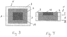
- FIG. 3 shows a plan view of an embodiment of a multi-layer carrier body and a section (right) through this along the line A-A '.
- a trough-shaped metal structure or functional area 2 is surrounded by a ceramic substrate 3 at the side surfaces and at the bottom.
- a further cuboid structure 33 that is to say a further region, of a further material, for example another ceramic material, is provided.
- This multi-layer carrier body 15 is constructed from three different types of film.
- the rectangular third area 33 is surrounded by the frame-shaped second and first areas 2, 3.
- the films In the underlying area II, the films have a second area 1 without an inner contour.
- the second area 2 is rectangular.
- the films In the lower area III, the films are printed over the whole area with the paste for the first Areal 3.
- a cavity may be provided. This is made up of films which have a recess, that is to say an unprinted area, at the corresponding location.
- FIG. 5 shows a further embodiment of a component carrier assembly with a component carrier 10 with a component 1 arranged thereon, which acts as a heat source.
- the illustration is a section along the vertical axis of the component carrier arrangement.
- FIG. 6 shows a section along the line AA 'through this component carrier assembly. The section runs in a plane parallel to the plane spanned by the longitudinal and transverse axes.
- FIGS. 5 and 6 shown embodiment of a component carrier assembly has in addition to the disposed on the top of the device 1, for example an LED, yet another discrete component 7, which is arranged in a cavity 8 in the bottom of the carrier body 15.
- This exemplary embodiment comprises three structured functional areas 2.
- a first functional area 2 extends below the component 1 arranged on the upper side and runs from the upper side of the carrier body 15 to the insulating layer 5.
- Functional area 2 has a cylindrical basic shape with a cross section whose round basic shape has a serrated edge, as in FIG FIG. 6 is apparent.
- From the vertical lateral surface horizontally extending regions 23 protrude into the substrate 3, which are formed as structured layers.
- These regions 23 running into the substrate may be a cross-sectional enlargement of the main body whose contour is at the same distance from the contour of the shell of the main body. You can alternatively be strip or web-shaped. Because of their shape, they can also be called an electrode structure. They improve the mechanical adaptation between metal and ceramic in the transition from the substrate to the functional area, for example by avoiding material tensions.
- an insulating layer 5 is provided between it and the heat sink. This extends below the component 1, but protruding beyond its base, but not over a large area over the entire underside of the multi-layer carrier body 15th
- the component carrier arrangement also has a second and third functional region 20, which extend between the conductor structure 4 on the upper side of the multi-layer carrier body 15 and a heat sink element 6 on the underside.
- These functional areas are cylindrical with a rectangular cross section. They can serve as a via or heat sink for another, not shown, component.
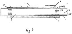
- FIG. 7 shows a further embodiment of a component carrier assembly with a component carrier 10 having a plurality of components 1 arranged thereon, which as Heat source act.
- the illustration is a section along the vertical axis of the component carrier arrangement.
- the spatial arrangement of the LEDs can be as in FIG. 9 be shown.
- the component carrier arrangement has a plurality of components 1 arranged on the upper side. These can be LEDs that develop heat during operation. Below the region in which the components 1 are arranged extends the structured functional region 2, which serves as a common heat sink for the components 1.
- the functional area 2 has a cylindrical basic body which extends from the upper side of the multi-layer carrier body 15 to the insulating layer 5. On the insulating layer 5, a common heat sink element 6 is provided. Furthermore, structured layers 23 are provided, which extend horizontally into the substrate 3. These are arranged on different levels one above the other. Above and below these areas, the substrate 3 extends.
- discrete component 7 is arranged on the upper side of the carrier body 15, which is, for example, an integrated NTC temperature sensor or an MLV element as ESD protection (ESD is short for English “electrostatic discharge ", that is, electrostatic discharge,) can act.
- ESD electrostatic discharge
- FIG. 8 shows a further embodiment of a component carrier arrangement comprising a component carrier 10 with a component 1 arranged thereon, which act as a heat source.
- the illustration is a section along the vertical axis of the component carrier arrangement.
- FIG. 9 shows a section along the line AA 'through this component carrier assembly. The section runs in a plane parallel to the plane spanned by the longitudinal and transverse axes.
- FIG. 9 shows the spatial arrangement of the components 1. One is arranged centrally, others are arranged in a ring around this component 1.
- FIG. 8 differs from the previous embodiment substantially by the structure of the functional area 2.
- an extended functional area 2 is provided as a heat sink for the components 1.
- the structured functional region 2 extends over a wide area, but is guided to the top or bottom only below the components and heat sinks.
- substrate regions 3 but also on the carrier body top side between the components 1.
- separate heat sink elements 6 are provided under the components 1.
- the functional area also has substrate areas in the lower area between regions of the functional area that extend to the heat sink elements 6.
- the extending in the upper and lower portions of the multi-layer carrier body areas of Functional area may be island-shaped, so that their cross-section substantially corresponds to the base of the components 1 or circular or annular, so that the components 1 are arranged on the circle or ring, as in FIG. 9 outlined.
- structured layers 23 protrude from the main body of the functional area into the substrate 3.
- FIG. 10 shows a section through a further embodiment, similar to that in the FIGS. 5 and 6 shown.
- an LED as a component 1 with high heat development and an MLV element as an exemplary further component 7 are arranged on a multi-layer carrier body 15.
- the component 1 is positioned under a lens 9.
- the width D1 of such an LED may be for example 1000 microns. It is fixed by solder, for example SnAgCu, on solder pads 18 on the carrier body 15.
- the width D7 of the further component 7 may be 300 ⁇ m. It is fixed to solder pads 17, for example comprising Ag / Ni / Sn.
- Such a multi-layer carrier body 15 may have a thickness D10 of 500 ⁇ m, wherein the substrate 3 has a thickness D15 of 400 ⁇ m.
- a first functional area 2, which serves as a thermal block or heat sink for the component 1, and two further functional areas 22 are arranged as plated-through holes below the further component 7.
- the width D2 of the integrated heat sink is 1500 ⁇ m both in the longitudinal and in the transverse direction.
- the distance to the edge of the carrier body is 700 ⁇ m (see FIG. 11 ).
- the width of the other functional areas corresponds to that of the further component 7.
- the width D2 of the main body of the integrated heat sink is 1500 ⁇ m both in the longitudinal and in the transverse direction.
- the distance D3 to the edge of the carrier body is 700 microns (see FIG. 9 ).
- the width of the further functional areas corresponds to that of the further component 7 and is 300 ⁇ m.
- the multi-layer carrier body 15 has a layered structure and includes a plurality of films that have been stacked and laminated to form the carrier body 15.
- the individual foils comprise substrate areas whose design corresponds to the section through the carrier body in the corresponding plane.
- Such films can be made by printing with different pastes for the different areas, which are then stacked and laminated. In this way it is possible to produce any structures within the substrate 3.
- the regions 23 protruding from the main body of the functional region can be produced in a simple manner, in that the printed functional region of such a layer protrudes beyond that of the underlying layer and the layer above it.
- structural regions of a film layer, or several film layers, which extend beyond the contours of the main body form the regions 23 projecting into the substrate 3.
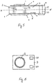
- FIG. 11 and FIG. 12 show two more sections through the device along the lines II and II-II in FIG. 10.
- FIG. 11 shows the section II, in which it is clearly visible that the LED is contacted by means of two contacts.
- section 2-2 it can be seen that the same applies to the further component 7.
Landscapes
- Engineering & Computer Science (AREA)
- Microelectronics & Electronic Packaging (AREA)
- Manufacturing & Machinery (AREA)
- Chemical & Material Sciences (AREA)
- Ceramic Engineering (AREA)
- Inorganic Chemistry (AREA)
- Cooling Or The Like Of Semiconductors Or Solid State Devices (AREA)
- Led Device Packages (AREA)
Applications Claiming Priority (2)
| Application Number | Priority Date | Filing Date | Title |
|---|---|---|---|
| DE102012113014.0A DE102012113014A1 (de) | 2012-12-21 | 2012-12-21 | Bauelementträger und Bauelementträgeranordnung |
| PCT/EP2013/076426 WO2014095587A1 (de) | 2012-12-21 | 2013-12-12 | Bauelementträger und bauelementträgeranordnung |
Publications (2)
| Publication Number | Publication Date |
|---|---|
| EP2936944A1 EP2936944A1 (de) | 2015-10-28 |
| EP2936944B1 true EP2936944B1 (de) | 2019-07-24 |
Family
ID=49759327
Family Applications (1)
| Application Number | Title | Priority Date | Filing Date |
|---|---|---|---|
| EP13803026.7A Not-in-force EP2936944B1 (de) | 2012-12-21 | 2013-12-12 | Bauelementträger und bauelementträgeranordnung |
Country Status (6)
| Country | Link |
|---|---|
| US (1) | US10021776B2 (enExample) |
| EP (1) | EP2936944B1 (enExample) |
| JP (2) | JP6401710B2 (enExample) |
| CN (1) | CN104854965B (enExample) |
| DE (1) | DE102012113014A1 (enExample) |
| WO (1) | WO2014095587A1 (enExample) |
Families Citing this family (5)
| Publication number | Priority date | Publication date | Assignee | Title |
|---|---|---|---|---|
| EP2838325B1 (en) | 2013-08-16 | 2021-06-16 | NGK Insulators, Ltd. | Ceramic circuit board and electronic device |
| EP2838327B1 (en) * | 2013-08-16 | 2018-11-14 | NGK Insulators, Ltd. | Heat dissipating circuit board and electronic device |
| DE102016107497B4 (de) * | 2016-03-24 | 2020-01-30 | Tdk Electronics Ag | Multi-LED System und Verfahren zu seiner Herstellung |
| DE102018115976A1 (de) * | 2017-07-10 | 2019-01-10 | Osram Opto Semiconductors Gmbh | Verfahren zum Bestücken eines Trägers mit Bauelementen, Pigment für das Bestücken eines Trägers mit einem Bauelement und Verfahren zur Herstellung eines Pigments |
| DE102017126268A1 (de) * | 2017-11-09 | 2019-05-09 | Osram Opto Semiconductors Gmbh | Träger, Anordnung mit einem Substrat und einem Träger und Verfahren zum Herstellen eines Trägers |
Family Cites Families (73)
| Publication number | Priority date | Publication date | Assignee | Title |
|---|---|---|---|---|
| JPS50143073A (enExample) | 1974-05-08 | 1975-11-18 | ||
| US4943470A (en) * | 1985-01-11 | 1990-07-24 | Ngk Spark Plug Co., Ltd. | Ceramic substrate for electrical devices |
| JPS6449247A (en) | 1987-08-19 | 1989-02-23 | Mitsubishi Electric Corp | Semiconductor light emitting device |
| US4922377A (en) * | 1987-11-16 | 1990-05-01 | Hitachi, Ltd. | Module and a substrate for the module |
| EP0475223B1 (en) * | 1990-08-31 | 1997-10-22 | Nec Corporation | Method of fabricating integrated circuit chip package |
| US5367765A (en) * | 1990-08-31 | 1994-11-29 | Nec Corporation | Method of fabricating integrated circuit chip package |
| US5285352A (en) * | 1992-07-15 | 1994-02-08 | Motorola, Inc. | Pad array semiconductor device with thermal conductor and process for making the same |
| JPH0758239A (ja) | 1993-06-30 | 1995-03-03 | Matsushita Electric Works Ltd | チップキャリア |
| JP3603354B2 (ja) | 1994-11-21 | 2004-12-22 | 株式会社デンソー | 混成集積回路装置 |
| JP3671457B2 (ja) * | 1995-06-07 | 2005-07-13 | 株式会社デンソー | 多層基板 |
| JP2950290B2 (ja) * | 1997-06-27 | 1999-09-20 | 日本電気株式会社 | 高周波集積回路装置およびその製造方法 |
| EP0926729A3 (en) * | 1997-12-10 | 1999-12-08 | Mitsubishi Gas Chemical Company, Inc. | Semiconductor plastic package and process for the production thereof |
| JP3635631B2 (ja) | 1999-12-20 | 2005-04-06 | 株式会社村田製作所 | 積層セラミック電子部品の製造方法 |
| JP3551876B2 (ja) | 2000-01-12 | 2004-08-11 | 株式会社村田製作所 | 積層セラミック電子部品の製造方法 |
| JP3805266B2 (ja) * | 2002-02-27 | 2006-08-02 | Uht株式会社 | セラミック積層体の製造装置 |
| JP3726035B2 (ja) | 2001-05-25 | 2005-12-14 | 京セラ株式会社 | セラミック積層体の製法 |
| JP4663173B2 (ja) | 2001-08-03 | 2011-03-30 | 京セラ株式会社 | セラミック積層体の製法 |
| US7089659B2 (en) | 2001-05-25 | 2006-08-15 | Kyocera Corporation | Method of producing ceramic laminates |
| JP3527899B2 (ja) | 2001-06-28 | 2004-05-17 | 京セラ株式会社 | 積層型電子部品およびその製法 |
| JP3784293B2 (ja) | 2001-09-27 | 2006-06-07 | 京セラ株式会社 | セラミック積層体の製法 |
| US7222419B2 (en) * | 2001-12-19 | 2007-05-29 | Chung-Shan Institute Of Science And Technology | Method of fabricating a ceramic substrate with a thermal conductive plug of a multi-chip package |
| JP2003197459A (ja) | 2001-12-26 | 2003-07-11 | Kyocera Corp | 積層型電子部品の製法 |
| JP2003209026A (ja) | 2002-01-11 | 2003-07-25 | Kyocera Corp | 積層型電子部品の製法 |
| JP2004079862A (ja) | 2002-08-21 | 2004-03-11 | Kyocera Corp | セラミック積層体の製法 |
| JP2004152908A (ja) | 2002-10-29 | 2004-05-27 | Kyocera Corp | セラミック積層体の製法 |
| JP4044830B2 (ja) | 2002-11-22 | 2008-02-06 | 京セラ株式会社 | 複合シートの製造方法、並びに積層部品の製造方法 |
| US20040134875A1 (en) * | 2002-11-22 | 2004-07-15 | Kyocera Corporation | Circuit-parts sheet and method of producing a multi-layer circuit board |
| JP2004253579A (ja) | 2003-02-20 | 2004-09-09 | Matsushita Electric Ind Co Ltd | 半導体装置 |
| CN101789482B (zh) * | 2003-03-10 | 2013-04-17 | 丰田合成株式会社 | 固体元件装置及其制造方法 |
| DE10313891A1 (de) * | 2003-03-27 | 2004-10-14 | Epcos Ag | Elektrisches Vielschichtbauelement |
| CN100481273C (zh) | 2003-03-31 | 2009-04-22 | Tdk株式会社 | 内部电极用糊料及电子部件的制造方法 |
| JP2005101367A (ja) | 2003-09-25 | 2005-04-14 | Kyocera Corp | 高周波モジュールおよび通信機器 |
| US7507682B2 (en) | 2004-02-24 | 2009-03-24 | Kyocera Corporation | Method of manufacturing ceramic paste and ceramic multi-layer wiring substrate utilizing the same |
| DE102004010001A1 (de) * | 2004-03-01 | 2005-09-22 | Epcos Ag | Elektrisches Bauelement und schaltungsanordnung mit dem Bauelement |
| US20080043444A1 (en) * | 2004-04-27 | 2008-02-21 | Kyocera Corporation | Wiring Board for Light-Emitting Element |
| JP2006156447A (ja) | 2004-11-25 | 2006-06-15 | Kyocera Corp | 発光素子用配線基板ならびに発光装置およびその製造方法 |
| DE102005042778A1 (de) * | 2004-09-09 | 2006-04-13 | Toyoda Gosei Co., Ltd., Nishikasugai | Optische Festkörpervorrichtung |
| JP4625972B2 (ja) * | 2004-12-06 | 2011-02-02 | スタンレー電気株式会社 | 表面実装型led |
| KR100596602B1 (ko) | 2005-03-30 | 2006-07-04 | 삼성전기주식회사 | 적층 세라믹 콘덴서 및 그 제조 방법 |
| JP4915058B2 (ja) | 2005-06-06 | 2012-04-11 | パナソニック株式会社 | Led部品およびその製造方法 |
| JP4915052B2 (ja) | 2005-04-01 | 2012-04-11 | パナソニック株式会社 | Led部品およびその製造方法 |
| US20070200133A1 (en) | 2005-04-01 | 2007-08-30 | Akira Hashimoto | Led assembly and manufacturing method |
| JP2007116217A (ja) | 2005-10-18 | 2007-05-10 | Hitachi Ltd | ミリ波レーダ装置およびそれを用いたミリ波レーダシステム |
| JP2007123677A (ja) | 2005-10-31 | 2007-05-17 | Matsushita Electric Ind Co Ltd | 積層セラミック基板の製造方法 |
| TWI306370B (en) * | 2006-03-31 | 2009-02-11 | Advanced Semiconductor Eng | Coreless thin substrate with embedded circuits in dielectric layer and method for manufacturing the same |
| WO2008002268A1 (en) | 2006-06-27 | 2008-01-03 | Agency For Science, Technology And Research | Ltcc substrate structure |
| US7999398B2 (en) * | 2006-08-03 | 2011-08-16 | Toyoda Gosei Co., Ltd. | Solid state device |
| JP4979299B2 (ja) * | 2006-08-03 | 2012-07-18 | 豊田合成株式会社 | 光学装置及びその製造方法 |
| US7919840B2 (en) * | 2007-11-20 | 2011-04-05 | International Business Machines Corporation | Integrated non-isolated VRM and microprocessor assembly |
| US8008682B2 (en) * | 2008-04-04 | 2011-08-30 | Hong Kong Applied Science And Technology Research Institute Co. Ltd. | Alumina substrate and method of making an alumina substrate |
| DE102008024480A1 (de) * | 2008-05-21 | 2009-12-03 | Epcos Ag | Elektrische Bauelementanordnung |
| DE102008024479A1 (de) * | 2008-05-21 | 2009-12-03 | Epcos Ag | Elektrische Bauelementanordnung |
| JP2010073767A (ja) * | 2008-09-17 | 2010-04-02 | Jtekt Corp | 多層回路基板 |
| CN101889353A (zh) * | 2008-09-28 | 2010-11-17 | 张义辉 | 交流电发光二极管模块 |
| JP5151933B2 (ja) | 2008-11-27 | 2013-02-27 | 株式会社Ihi | 電子機器用放熱器 |
| JP2010171157A (ja) | 2009-01-22 | 2010-08-05 | Sanyo Electric Co Ltd | 電子素子用パッケージ及び電子部品 |
| DE102009010179A1 (de) * | 2009-02-23 | 2010-09-02 | Osram Gesellschaft mit beschränkter Haftung | Leuchtmodul mit Reflektorwand |
| US8256685B2 (en) * | 2009-06-30 | 2012-09-04 | International Business Machines Corporation | Compact millimeter wave packages with integrated antennas |
| US8933556B2 (en) | 2010-01-22 | 2015-01-13 | Ibiden Co., Ltd. | Wiring board |
| TWI501380B (zh) * | 2010-01-29 | 2015-09-21 | Nat Chip Implementation Ct Nat Applied Res Lab | 多基板晶片模組堆疊之三維系統晶片結構 |
| EP2381451B1 (en) | 2010-04-22 | 2018-08-01 | Epcos AG | Method for producing an electrical multi-layer component and electrical multi-layer component |
| EP2437581A1 (de) * | 2010-09-30 | 2012-04-04 | Odelo GmbH | Leuchtdiode auf Keramiksubstratbasis |
| JP5862574B2 (ja) | 2010-11-19 | 2016-02-16 | 旭硝子株式会社 | 発光素子用基板および発光装置 |
| JP2012204754A (ja) | 2011-03-28 | 2012-10-22 | Toppan Printing Co Ltd | Led発光素子用リードフレーム、およびその製造方法、並びにそれを用いたledパッケージ |
| JP2012204783A (ja) | 2011-03-28 | 2012-10-22 | Stanley Electric Co Ltd | 発光ダイオード装置 |
| KR101869552B1 (ko) | 2011-05-13 | 2018-06-21 | 엘지이노텍 주식회사 | 발광 소자 패키지 및 이를 구비한 자외선 램프 |
| JP5968674B2 (ja) | 2011-05-13 | 2016-08-10 | エルジー イノテック カンパニー リミテッド | 発光素子パッケージ及びこれを備える紫外線ランプ |
| JP6010292B2 (ja) * | 2011-11-01 | 2016-10-19 | 太陽誘電株式会社 | 弾性波デバイス |
| CN103999210B (zh) * | 2011-12-22 | 2016-11-02 | 京瓷株式会社 | 布线基板以及电子装置 |
| US20130337648A1 (en) * | 2012-06-14 | 2013-12-19 | Bridge Semiconductor Corporation | Method of making cavity substrate with built-in stiffener and cavity |
| DE102012108107A1 (de) * | 2012-08-31 | 2014-03-27 | Epcos Ag | Leuchtdiodenvorrichtung |
| KR20140039740A (ko) * | 2012-09-25 | 2014-04-02 | 엘지이노텍 주식회사 | 발광소자 패키지 |
| DE102012113018A1 (de) * | 2012-12-21 | 2014-06-26 | Epcos Ag | Verfahren zur Herstellung eines Mehrschichtträgerkörpers |
-
2012
- 2012-12-21 DE DE102012113014.0A patent/DE102012113014A1/de not_active Ceased
-
2013
- 2013-12-12 EP EP13803026.7A patent/EP2936944B1/de not_active Not-in-force
- 2013-12-12 WO PCT/EP2013/076426 patent/WO2014095587A1/de not_active Ceased
- 2013-12-12 US US14/654,369 patent/US10021776B2/en active Active
- 2013-12-12 JP JP2015548377A patent/JP6401710B2/ja not_active Expired - Fee Related
- 2013-12-12 CN CN201380067199.3A patent/CN104854965B/zh not_active Expired - Fee Related
-
2018
- 2018-05-14 JP JP2018093237A patent/JP2018139317A/ja active Pending
Non-Patent Citations (1)
| Title |
|---|
| None * |
Also Published As
| Publication number | Publication date |
|---|---|
| JP2018139317A (ja) | 2018-09-06 |
| DE102012113014A1 (de) | 2014-06-26 |
| CN104854965B (zh) | 2019-01-01 |
| JP6401710B2 (ja) | 2018-10-10 |
| EP2936944A1 (de) | 2015-10-28 |
| CN104854965A (zh) | 2015-08-19 |
| US20150342027A1 (en) | 2015-11-26 |
| WO2014095587A1 (de) | 2014-06-26 |
| US10021776B2 (en) | 2018-07-10 |
| JP2016500485A (ja) | 2016-01-12 |
Similar Documents
| Publication | Publication Date | Title |
|---|---|---|
| DE102012215788B4 (de) | Mehrlagige LED-Leiterplatte | |
| DE102016218522B3 (de) | Optische oder optoelektronische Baugruppe und Verfahren zur Herstellung dafür | |
| EP3542399B1 (de) | Leistungsmodul mit verringerter defektanfälligkeit und verwendung desselben | |
| EP2524394B1 (de) | Elektronisches bauteil, verfahren zu dessen herstellung und leiterplatte mit elektronischem bauteil | |
| EP2936944B1 (de) | Bauelementträger und bauelementträgeranordnung | |
| EP3469629B1 (de) | Eine vielzahl von modulen | |
| DE102015215133B4 (de) | Halbleitervorrichtung | |
| DE102014100309B4 (de) | Chipanordnung und Verfahren zum Bilden einer Chipanordnung | |
| DE102009033029A1 (de) | Elektronische Vorrichtung | |
| WO2017182159A1 (de) | Vielschicht-trägersystem, verfahren zur herstellung eines vielschicht-trägersystems und verwendung eines vielschicht-trägersystems | |
| DE102010050342A1 (de) | Laminat mit integriertem elektronischen Bauteil | |
| WO2012152364A1 (de) | Substrat mit elektrisch neutralem bereich | |
| DE102018215686A1 (de) | Leiterplatte und Planer Transformatorgebiet der Erfindung | |
| EP2054947B1 (de) | Optoelektronisches bauelement | |
| DE102012215934B4 (de) | Lichtsystem | |
| WO2013004455A1 (de) | Verfahren zur herstellung einer leuchtvorrichtung und leuchtvorrichtung | |
| DE102019116021B4 (de) | Flexible Leiterplatte mit thermisch leitender Verbindung zu einer Wärmesenke | |
| DE102016107497B4 (de) | Multi-LED System und Verfahren zu seiner Herstellung | |
| DE102014109385A1 (de) | Elektronische Bauteilanordnung | |
| DE102020100742B4 (de) | Lichtmodul, Beleuchtungseinrichtung und Kraftfahrzeug | |
| EP2936950B1 (de) | Verfahren zur herstellung eines mehrschichtträgerkörpers | |
| DE102019113714B4 (de) | Adapterelement zum Anbinden eines Elektronikbauteils an ein Kühlkörperelement, System mit einem solchen Adapterelement und Verfahren zum Herstellen eines solchen Adapterelements | |
| DE102017203217A1 (de) | Kontaktanordnung | |
| DE102009050178B3 (de) | Leistungshalbleitermodul mit einem eine dreidimensionale Oberflächenkontur aufweisenden Substrat sowie Herstellungsverfahren hierzu | |
| DE102011086546A1 (de) | Anordnung aus einem optoelektronischen bauelement und einer leiterplatte |
Legal Events
| Date | Code | Title | Description |
|---|---|---|---|
| PUAI | Public reference made under article 153(3) epc to a published international application that has entered the european phase |
Free format text: ORIGINAL CODE: 0009012 |
|
| 17P | Request for examination filed |
Effective date: 20150603 |
|
| AK | Designated contracting states |
Kind code of ref document: A1 Designated state(s): AL AT BE BG CH CY CZ DE DK EE ES FI FR GB GR HR HU IE IS IT LI LT LU LV MC MK MT NL NO PL PT RO RS SE SI SK SM TR |
|
| AX | Request for extension of the european patent |
Extension state: BA ME |
|
| DAX | Request for extension of the european patent (deleted) | ||
| RAP1 | Party data changed (applicant data changed or rights of an application transferred) |
Owner name: EPCOS AG |
|
| STAA | Information on the status of an ep patent application or granted ep patent |
Free format text: STATUS: EXAMINATION IS IN PROGRESS |
|
| 17Q | First examination report despatched |
Effective date: 20180613 |
|
| RAP1 | Party data changed (applicant data changed or rights of an application transferred) |
Owner name: TDK ELECTRONICS AG |
|
| RIC1 | Information provided on ipc code assigned before grant |
Ipc: H05K 1/03 20060101ALI20190205BHEP Ipc: H05K 3/00 20060101ALI20190205BHEP Ipc: H01L 33/64 20100101ALI20190205BHEP Ipc: H05K 1/02 20060101AFI20190205BHEP |
|
| GRAP | Despatch of communication of intention to grant a patent |
Free format text: ORIGINAL CODE: EPIDOSNIGR1 |
|
| STAA | Information on the status of an ep patent application or granted ep patent |
Free format text: STATUS: GRANT OF PATENT IS INTENDED |
|
| INTG | Intention to grant announced |
Effective date: 20190321 |
|
| GRAS | Grant fee paid |
Free format text: ORIGINAL CODE: EPIDOSNIGR3 |
|
| GRAA | (expected) grant |
Free format text: ORIGINAL CODE: 0009210 |
|
| STAA | Information on the status of an ep patent application or granted ep patent |
Free format text: STATUS: THE PATENT HAS BEEN GRANTED |
|
| AK | Designated contracting states |
Kind code of ref document: B1 Designated state(s): AL AT BE BG CH CY CZ DE DK EE ES FI FR GB GR HR HU IE IS IT LI LT LU LV MC MK MT NL NO PL PT RO RS SE SI SK SM TR |
|
| REG | Reference to a national code |
Ref country code: GB Ref legal event code: FG4D Free format text: NOT ENGLISH |
|
| REG | Reference to a national code |
Ref country code: CH Ref legal event code: EP |
|
| REG | Reference to a national code |
Ref country code: DE Ref legal event code: R096 Ref document number: 502013013236 Country of ref document: DE |
|
| REG | Reference to a national code |
Ref country code: AT Ref legal event code: REF Ref document number: 1159893 Country of ref document: AT Kind code of ref document: T Effective date: 20190815 |
|
| REG | Reference to a national code |
Ref country code: IE Ref legal event code: FG4D Free format text: LANGUAGE OF EP DOCUMENT: GERMAN |
|
| REG | Reference to a national code |
Ref country code: NL Ref legal event code: MP Effective date: 20190724 |
|
| REG | Reference to a national code |
Ref country code: LT Ref legal event code: MG4D |
|
| PG25 | Lapsed in a contracting state [announced via postgrant information from national office to epo] |
Ref country code: LT Free format text: LAPSE BECAUSE OF FAILURE TO SUBMIT A TRANSLATION OF THE DESCRIPTION OR TO PAY THE FEE WITHIN THE PRESCRIBED TIME-LIMIT Effective date: 20190724 Ref country code: HR Free format text: LAPSE BECAUSE OF FAILURE TO SUBMIT A TRANSLATION OF THE DESCRIPTION OR TO PAY THE FEE WITHIN THE PRESCRIBED TIME-LIMIT Effective date: 20190724 Ref country code: NL Free format text: LAPSE BECAUSE OF FAILURE TO SUBMIT A TRANSLATION OF THE DESCRIPTION OR TO PAY THE FEE WITHIN THE PRESCRIBED TIME-LIMIT Effective date: 20190724 Ref country code: PT Free format text: LAPSE BECAUSE OF FAILURE TO SUBMIT A TRANSLATION OF THE DESCRIPTION OR TO PAY THE FEE WITHIN THE PRESCRIBED TIME-LIMIT Effective date: 20191125 Ref country code: BG Free format text: LAPSE BECAUSE OF FAILURE TO SUBMIT A TRANSLATION OF THE DESCRIPTION OR TO PAY THE FEE WITHIN THE PRESCRIBED TIME-LIMIT Effective date: 20191024 Ref country code: NO Free format text: LAPSE BECAUSE OF FAILURE TO SUBMIT A TRANSLATION OF THE DESCRIPTION OR TO PAY THE FEE WITHIN THE PRESCRIBED TIME-LIMIT Effective date: 20191024 Ref country code: SE Free format text: LAPSE BECAUSE OF FAILURE TO SUBMIT A TRANSLATION OF THE DESCRIPTION OR TO PAY THE FEE WITHIN THE PRESCRIBED TIME-LIMIT Effective date: 20190724 Ref country code: FI Free format text: LAPSE BECAUSE OF FAILURE TO SUBMIT A TRANSLATION OF THE DESCRIPTION OR TO PAY THE FEE WITHIN THE PRESCRIBED TIME-LIMIT Effective date: 20190724 |
|
| PG25 | Lapsed in a contracting state [announced via postgrant information from national office to epo] |
Ref country code: RS Free format text: LAPSE BECAUSE OF FAILURE TO SUBMIT A TRANSLATION OF THE DESCRIPTION OR TO PAY THE FEE WITHIN THE PRESCRIBED TIME-LIMIT Effective date: 20190724 Ref country code: GR Free format text: LAPSE BECAUSE OF FAILURE TO SUBMIT A TRANSLATION OF THE DESCRIPTION OR TO PAY THE FEE WITHIN THE PRESCRIBED TIME-LIMIT Effective date: 20191025 Ref country code: IS Free format text: LAPSE BECAUSE OF FAILURE TO SUBMIT A TRANSLATION OF THE DESCRIPTION OR TO PAY THE FEE WITHIN THE PRESCRIBED TIME-LIMIT Effective date: 20191124 Ref country code: AL Free format text: LAPSE BECAUSE OF FAILURE TO SUBMIT A TRANSLATION OF THE DESCRIPTION OR TO PAY THE FEE WITHIN THE PRESCRIBED TIME-LIMIT Effective date: 20190724 Ref country code: ES Free format text: LAPSE BECAUSE OF FAILURE TO SUBMIT A TRANSLATION OF THE DESCRIPTION OR TO PAY THE FEE WITHIN THE PRESCRIBED TIME-LIMIT Effective date: 20190724 Ref country code: LV Free format text: LAPSE BECAUSE OF FAILURE TO SUBMIT A TRANSLATION OF THE DESCRIPTION OR TO PAY THE FEE WITHIN THE PRESCRIBED TIME-LIMIT Effective date: 20190724 |
|
| PG25 | Lapsed in a contracting state [announced via postgrant information from national office to epo] |
Ref country code: TR Free format text: LAPSE BECAUSE OF FAILURE TO SUBMIT A TRANSLATION OF THE DESCRIPTION OR TO PAY THE FEE WITHIN THE PRESCRIBED TIME-LIMIT Effective date: 20190724 |
|
| PG25 | Lapsed in a contracting state [announced via postgrant information from national office to epo] |
Ref country code: PL Free format text: LAPSE BECAUSE OF FAILURE TO SUBMIT A TRANSLATION OF THE DESCRIPTION OR TO PAY THE FEE WITHIN THE PRESCRIBED TIME-LIMIT Effective date: 20190724 Ref country code: EE Free format text: LAPSE BECAUSE OF FAILURE TO SUBMIT A TRANSLATION OF THE DESCRIPTION OR TO PAY THE FEE WITHIN THE PRESCRIBED TIME-LIMIT Effective date: 20190724 Ref country code: IT Free format text: LAPSE BECAUSE OF FAILURE TO SUBMIT A TRANSLATION OF THE DESCRIPTION OR TO PAY THE FEE WITHIN THE PRESCRIBED TIME-LIMIT Effective date: 20190724 Ref country code: DK Free format text: LAPSE BECAUSE OF FAILURE TO SUBMIT A TRANSLATION OF THE DESCRIPTION OR TO PAY THE FEE WITHIN THE PRESCRIBED TIME-LIMIT Effective date: 20190724 Ref country code: RO Free format text: LAPSE BECAUSE OF FAILURE TO SUBMIT A TRANSLATION OF THE DESCRIPTION OR TO PAY THE FEE WITHIN THE PRESCRIBED TIME-LIMIT Effective date: 20190724 |
|
| PG25 | Lapsed in a contracting state [announced via postgrant information from national office to epo] |
Ref country code: IS Free format text: LAPSE BECAUSE OF FAILURE TO SUBMIT A TRANSLATION OF THE DESCRIPTION OR TO PAY THE FEE WITHIN THE PRESCRIBED TIME-LIMIT Effective date: 20200224 Ref country code: SK Free format text: LAPSE BECAUSE OF FAILURE TO SUBMIT A TRANSLATION OF THE DESCRIPTION OR TO PAY THE FEE WITHIN THE PRESCRIBED TIME-LIMIT Effective date: 20190724 Ref country code: CZ Free format text: LAPSE BECAUSE OF FAILURE TO SUBMIT A TRANSLATION OF THE DESCRIPTION OR TO PAY THE FEE WITHIN THE PRESCRIBED TIME-LIMIT Effective date: 20190724 Ref country code: SM Free format text: LAPSE BECAUSE OF FAILURE TO SUBMIT A TRANSLATION OF THE DESCRIPTION OR TO PAY THE FEE WITHIN THE PRESCRIBED TIME-LIMIT Effective date: 20190724 |
|
| REG | Reference to a national code |
Ref country code: DE Ref legal event code: R097 Ref document number: 502013013236 Country of ref document: DE |
|
| PLBE | No opposition filed within time limit |
Free format text: ORIGINAL CODE: 0009261 |
|
| STAA | Information on the status of an ep patent application or granted ep patent |
Free format text: STATUS: NO OPPOSITION FILED WITHIN TIME LIMIT |
|
| PG2D | Information on lapse in contracting state deleted |
Ref country code: IS |
|
| REG | Reference to a national code |
Ref country code: CH Ref legal event code: PL |
|
| 26N | No opposition filed |
Effective date: 20200603 |
|
| REG | Reference to a national code |
Ref country code: BE Ref legal event code: MM Effective date: 20191231 |
|
| PG25 | Lapsed in a contracting state [announced via postgrant information from national office to epo] |
Ref country code: SI Free format text: LAPSE BECAUSE OF FAILURE TO SUBMIT A TRANSLATION OF THE DESCRIPTION OR TO PAY THE FEE WITHIN THE PRESCRIBED TIME-LIMIT Effective date: 20190724 Ref country code: MC Free format text: LAPSE BECAUSE OF FAILURE TO SUBMIT A TRANSLATION OF THE DESCRIPTION OR TO PAY THE FEE WITHIN THE PRESCRIBED TIME-LIMIT Effective date: 20190724 |
|
| GBPC | Gb: european patent ceased through non-payment of renewal fee |
Effective date: 20191212 |
|
| PG25 | Lapsed in a contracting state [announced via postgrant information from national office to epo] |
Ref country code: LU Free format text: LAPSE BECAUSE OF NON-PAYMENT OF DUE FEES Effective date: 20191212 Ref country code: GB Free format text: LAPSE BECAUSE OF NON-PAYMENT OF DUE FEES Effective date: 20191212 Ref country code: IE Free format text: LAPSE BECAUSE OF NON-PAYMENT OF DUE FEES Effective date: 20191212 Ref country code: FR Free format text: LAPSE BECAUSE OF NON-PAYMENT OF DUE FEES Effective date: 20191231 |
|
| PG25 | Lapsed in a contracting state [announced via postgrant information from national office to epo] |
Ref country code: CH Free format text: LAPSE BECAUSE OF NON-PAYMENT OF DUE FEES Effective date: 20191231 Ref country code: LI Free format text: LAPSE BECAUSE OF NON-PAYMENT OF DUE FEES Effective date: 20191231 Ref country code: BE Free format text: LAPSE BECAUSE OF NON-PAYMENT OF DUE FEES Effective date: 20191231 |
|
| REG | Reference to a national code |
Ref country code: AT Ref legal event code: MM01 Ref document number: 1159893 Country of ref document: AT Kind code of ref document: T Effective date: 20191212 |
|
| PG25 | Lapsed in a contracting state [announced via postgrant information from national office to epo] |
Ref country code: CY Free format text: LAPSE BECAUSE OF FAILURE TO SUBMIT A TRANSLATION OF THE DESCRIPTION OR TO PAY THE FEE WITHIN THE PRESCRIBED TIME-LIMIT Effective date: 20190724 Ref country code: AT Free format text: LAPSE BECAUSE OF NON-PAYMENT OF DUE FEES Effective date: 20191212 |
|
| PG25 | Lapsed in a contracting state [announced via postgrant information from national office to epo] |
Ref country code: MT Free format text: LAPSE BECAUSE OF FAILURE TO SUBMIT A TRANSLATION OF THE DESCRIPTION OR TO PAY THE FEE WITHIN THE PRESCRIBED TIME-LIMIT Effective date: 20190724 Ref country code: HU Free format text: LAPSE BECAUSE OF FAILURE TO SUBMIT A TRANSLATION OF THE DESCRIPTION OR TO PAY THE FEE WITHIN THE PRESCRIBED TIME-LIMIT; INVALID AB INITIO Effective date: 20131212 |
|
| PG25 | Lapsed in a contracting state [announced via postgrant information from national office to epo] |
Ref country code: MK Free format text: LAPSE BECAUSE OF FAILURE TO SUBMIT A TRANSLATION OF THE DESCRIPTION OR TO PAY THE FEE WITHIN THE PRESCRIBED TIME-LIMIT Effective date: 20190724 |
|
| PGFP | Annual fee paid to national office [announced via postgrant information from national office to epo] |
Ref country code: DE Payment date: 20221219 Year of fee payment: 10 |
|
| P01 | Opt-out of the competence of the unified patent court (upc) registered |
Effective date: 20230521 |
|
| REG | Reference to a national code |
Ref country code: DE Ref legal event code: R119 Ref document number: 502013013236 Country of ref document: DE |
|
| PG25 | Lapsed in a contracting state [announced via postgrant information from national office to epo] |
Ref country code: DE Free format text: LAPSE BECAUSE OF NON-PAYMENT OF DUE FEES Effective date: 20240702 |
|
| PG25 | Lapsed in a contracting state [announced via postgrant information from national office to epo] |
Ref country code: DE Free format text: LAPSE BECAUSE OF NON-PAYMENT OF DUE FEES Effective date: 20240702 |