EP2802013A1 - Halbleiterbauelement - Google Patents
Halbleiterbauelement Download PDFInfo
- Publication number
- EP2802013A1 EP2802013A1 EP14173340.2A EP14173340A EP2802013A1 EP 2802013 A1 EP2802013 A1 EP 2802013A1 EP 14173340 A EP14173340 A EP 14173340A EP 2802013 A1 EP2802013 A1 EP 2802013A1
- Authority
- EP
- European Patent Office
- Prior art keywords
- feed
- semiconductor device
- layer
- throughs
- trenches
- Prior art date
- Legal status (The legal status is an assumption and is not a legal conclusion. Google has not performed a legal analysis and makes no representation as to the accuracy of the status listed.)
- Granted
Links
Images




Classifications
-
- H—ELECTRICITY
- H10—SEMICONDUCTOR DEVICES; ELECTRIC SOLID-STATE DEVICES NOT OTHERWISE PROVIDED FOR
- H10D—INORGANIC ELECTRIC SEMICONDUCTOR DEVICES
- H10D30/00—Field-effect transistors [FET]
- H10D30/60—Insulated-gate field-effect transistors [IGFET]
- H10D30/64—Double-diffused metal-oxide semiconductor [DMOS] FETs
- H10D30/66—Vertical DMOS [VDMOS] FETs
- H10D30/663—Vertical DMOS [VDMOS] FETs having both source contacts and drain contacts on the same surface, i.e. up-drain VDMOS
-
- H—ELECTRICITY
- H10—SEMICONDUCTOR DEVICES; ELECTRIC SOLID-STATE DEVICES NOT OTHERWISE PROVIDED FOR
- H10D—INORGANIC ELECTRIC SEMICONDUCTOR DEVICES
- H10D30/00—Field-effect transistors [FET]
- H10D30/01—Manufacture or treatment
- H10D30/021—Manufacture or treatment of FETs having insulated gates [IGFET]
- H10D30/028—Manufacture or treatment of FETs having insulated gates [IGFET] of double-diffused metal oxide semiconductor [DMOS] FETs
- H10D30/0291—Manufacture or treatment of FETs having insulated gates [IGFET] of double-diffused metal oxide semiconductor [DMOS] FETs of vertical DMOS [VDMOS] FETs
- H10D30/0297—Manufacture or treatment of FETs having insulated gates [IGFET] of double-diffused metal oxide semiconductor [DMOS] FETs of vertical DMOS [VDMOS] FETs using recessing of the gate electrodes, e.g. to form trench gate electrodes
-
- H—ELECTRICITY
- H10—SEMICONDUCTOR DEVICES; ELECTRIC SOLID-STATE DEVICES NOT OTHERWISE PROVIDED FOR
- H10D—INORGANIC ELECTRIC SEMICONDUCTOR DEVICES
- H10D30/00—Field-effect transistors [FET]
- H10D30/60—Insulated-gate field-effect transistors [IGFET]
- H10D30/64—Double-diffused metal-oxide semiconductor [DMOS] FETs
- H10D30/66—Vertical DMOS [VDMOS] FETs
- H10D30/668—Vertical DMOS [VDMOS] FETs having trench gate electrodes, e.g. UMOS transistors
-
- H—ELECTRICITY
- H10—SEMICONDUCTOR DEVICES; ELECTRIC SOLID-STATE DEVICES NOT OTHERWISE PROVIDED FOR
- H10D—INORGANIC ELECTRIC SEMICONDUCTOR DEVICES
- H10D64/00—Electrodes of devices having potential barriers
- H10D64/118—Electrodes comprising insulating layers having particular dielectric or electrostatic properties, e.g. having static charges
-
- H—ELECTRICITY
- H10—SEMICONDUCTOR DEVICES; ELECTRIC SOLID-STATE DEVICES NOT OTHERWISE PROVIDED FOR
- H10D—INORGANIC ELECTRIC SEMICONDUCTOR DEVICES
- H10D64/00—Electrodes of devices having potential barriers
- H10D64/20—Electrodes characterised by their shapes, relative sizes or dispositions
- H10D64/23—Electrodes carrying the current to be rectified, amplified, oscillated or switched, e.g. sources, drains, anodes or cathodes
- H10D64/251—Source or drain electrodes for field-effect devices
- H10D64/256—Source or drain electrodes for field-effect devices for lateral devices wherein the source or drain electrodes are recessed in semiconductor bodies
-
- H—ELECTRICITY
- H10—SEMICONDUCTOR DEVICES; ELECTRIC SOLID-STATE DEVICES NOT OTHERWISE PROVIDED FOR
- H10D—INORGANIC ELECTRIC SEMICONDUCTOR DEVICES
- H10D64/00—Electrodes of devices having potential barriers
- H10D64/60—Electrodes characterised by their materials
- H10D64/62—Electrodes ohmically coupled to a semiconductor
-
- H—ELECTRICITY
- H10—SEMICONDUCTOR DEVICES; ELECTRIC SOLID-STATE DEVICES NOT OTHERWISE PROVIDED FOR
- H10W—GENERIC PACKAGES, INTERCONNECTIONS, CONNECTORS OR OTHER CONSTRUCTIONAL DETAILS OF DEVICES COVERED BY CLASS H10
- H10W72/00—Interconnections or connectors in packages
- H10W72/01—Manufacture or treatment
- H10W72/012—Manufacture or treatment of bump connectors, dummy bumps or thermal bumps
-
- H—ELECTRICITY
- H10—SEMICONDUCTOR DEVICES; ELECTRIC SOLID-STATE DEVICES NOT OTHERWISE PROVIDED FOR
- H10W—GENERIC PACKAGES, INTERCONNECTIONS, CONNECTORS OR OTHER CONSTRUCTIONAL DETAILS OF DEVICES COVERED BY CLASS H10
- H10W72/00—Interconnections or connectors in packages
- H10W72/20—Bump connectors, e.g. solder bumps or copper pillars; Dummy bumps; Thermal bumps
-
- H—ELECTRICITY
- H10—SEMICONDUCTOR DEVICES; ELECTRIC SOLID-STATE DEVICES NOT OTHERWISE PROVIDED FOR
- H10D—INORGANIC ELECTRIC SEMICONDUCTOR DEVICES
- H10D62/00—Semiconductor bodies, or regions thereof, of devices having potential barriers
- H10D62/80—Semiconductor bodies, or regions thereof, of devices having potential barriers characterised by the materials
- H10D62/83—Semiconductor bodies, or regions thereof, of devices having potential barriers characterised by the materials being Group IV materials, e.g. B-doped Si or undoped Ge
-
- H—ELECTRICITY
- H10—SEMICONDUCTOR DEVICES; ELECTRIC SOLID-STATE DEVICES NOT OTHERWISE PROVIDED FOR
- H10W—GENERIC PACKAGES, INTERCONNECTIONS, CONNECTORS OR OTHER CONSTRUCTIONAL DETAILS OF DEVICES COVERED BY CLASS H10
- H10W72/00—Interconnections or connectors in packages
- H10W72/20—Bump connectors, e.g. solder bumps or copper pillars; Dummy bumps; Thermal bumps
- H10W72/221—Structures or relative sizes
-
- H—ELECTRICITY
- H10—SEMICONDUCTOR DEVICES; ELECTRIC SOLID-STATE DEVICES NOT OTHERWISE PROVIDED FOR
- H10W—GENERIC PACKAGES, INTERCONNECTIONS, CONNECTORS OR OTHER CONSTRUCTIONAL DETAILS OF DEVICES COVERED BY CLASS H10
- H10W72/00—Interconnections or connectors in packages
- H10W72/20—Bump connectors, e.g. solder bumps or copper pillars; Dummy bumps; Thermal bumps
- H10W72/231—Shapes
- H10W72/232—Plan-view shape, i.e. in top view
-
- H—ELECTRICITY
- H10—SEMICONDUCTOR DEVICES; ELECTRIC SOLID-STATE DEVICES NOT OTHERWISE PROVIDED FOR
- H10W—GENERIC PACKAGES, INTERCONNECTIONS, CONNECTORS OR OTHER CONSTRUCTIONAL DETAILS OF DEVICES COVERED BY CLASS H10
- H10W72/00—Interconnections or connectors in packages
- H10W72/20—Bump connectors, e.g. solder bumps or copper pillars; Dummy bumps; Thermal bumps
- H10W72/241—Dispositions, e.g. layouts
- H10W72/242—Dispositions, e.g. layouts relative to the surface, e.g. recessed, protruding
-
- H—ELECTRICITY
- H10—SEMICONDUCTOR DEVICES; ELECTRIC SOLID-STATE DEVICES NOT OTHERWISE PROVIDED FOR
- H10W—GENERIC PACKAGES, INTERCONNECTIONS, CONNECTORS OR OTHER CONSTRUCTIONAL DETAILS OF DEVICES COVERED BY CLASS H10
- H10W72/00—Interconnections or connectors in packages
- H10W72/20—Bump connectors, e.g. solder bumps or copper pillars; Dummy bumps; Thermal bumps
- H10W72/251—Materials
-
- H—ELECTRICITY
- H10—SEMICONDUCTOR DEVICES; ELECTRIC SOLID-STATE DEVICES NOT OTHERWISE PROVIDED FOR
- H10W—GENERIC PACKAGES, INTERCONNECTIONS, CONNECTORS OR OTHER CONSTRUCTIONAL DETAILS OF DEVICES COVERED BY CLASS H10
- H10W72/00—Interconnections or connectors in packages
- H10W72/20—Bump connectors, e.g. solder bumps or copper pillars; Dummy bumps; Thermal bumps
- H10W72/29—Bond pads specially adapted therefor
-
- H—ELECTRICITY
- H10—SEMICONDUCTOR DEVICES; ELECTRIC SOLID-STATE DEVICES NOT OTHERWISE PROVIDED FOR
- H10W—GENERIC PACKAGES, INTERCONNECTIONS, CONNECTORS OR OTHER CONSTRUCTIONAL DETAILS OF DEVICES COVERED BY CLASS H10
- H10W72/00—Interconnections or connectors in packages
- H10W72/90—Bond pads, in general
-
- H—ELECTRICITY
- H10—SEMICONDUCTOR DEVICES; ELECTRIC SOLID-STATE DEVICES NOT OTHERWISE PROVIDED FOR
- H10W—GENERIC PACKAGES, INTERCONNECTIONS, CONNECTORS OR OTHER CONSTRUCTIONAL DETAILS OF DEVICES COVERED BY CLASS H10
- H10W72/00—Interconnections or connectors in packages
- H10W72/90—Bond pads, in general
- H10W72/931—Shapes of bond pads
- H10W72/932—Plan-view shape, i.e. in top view
-
- H—ELECTRICITY
- H10—SEMICONDUCTOR DEVICES; ELECTRIC SOLID-STATE DEVICES NOT OTHERWISE PROVIDED FOR
- H10W—GENERIC PACKAGES, INTERCONNECTIONS, CONNECTORS OR OTHER CONSTRUCTIONAL DETAILS OF DEVICES COVERED BY CLASS H10
- H10W72/00—Interconnections or connectors in packages
- H10W72/90—Bond pads, in general
- H10W72/931—Shapes of bond pads
- H10W72/936—Multiple bond pads having different shapes
Definitions
- Embodiments in accordance with the present teaching generally pertain to semiconductor devices.
- a “flip chip” is a semiconductor device that includes a pattern of solder balls arrayed on one of the chip's surfaces. During fabrication, the solder balls are formed on the top surface of the chip. The chip can then be readily mounted onto, for example, a circuit board by flipping the chip so that the top surface faces downward and the solder balls are aligned with corresponding pads on the circuit board.
- the gate and source contacts are on one surface (e.g., the top surface) of the chip while the drain contact is on the opposite surface (e.g., the bottom surface) of the chip.
- the gate, source, and drain contacts are on the same surface of the chip.
- a "diffusion sinker" or “deep sinker” 110 is formed in the epitaxial layer 150 between the drain 120 and the substrate layer 130 as shown in Figure 1 . In operation, current will flow from the source 140 to, and through, the substrate and then to the drain in a known manner.
- the sinker is formed using an isotropic diffusion process in which a dopant material is diffused through the epitaxial layer until the sinker is in contact with the substrate.
- a dopant material is diffused through the epitaxial layer until the sinker is in contact with the substrate.
- the sinker diffuses downward (in the y-direction)
- it also diffuses both along the surface of the structure (in the x-direction) and into the higher resistivity epitaxial layer.
- the surface area of the sinker is relatively large, increasing the size of each cell and thereby decreasing cell density.
- the resistance of the epitaxial layer increases as the size of the sinker increases, thereby increasing the device's on-resistance (Rdson).
- the isotropic diffusion process is relatively slow, which increases the time needed to manufacture the flip chips and decreases throughput, thereby increasing costs.
- a semiconductor device e.g., a flip chip
- a substrate layer that is separated from a drain contact by an intervening layer.
- Trench-like feed-through elements that pass through the intervening layer are used to electrically connect the drain contact and the substrate layer when the device is operated.
- Embodiments according to the present teaching provide solutions to the problems associated with sinkers.
- relatively deep trenches filled with a conductive material such as tungsten are used to connect the drain contact to the substrate.
- the trenches - also referred to herein as "feed-throughs" - occupy less surface area and result in lower parasitic resistance in the epitaxial layer.
- feed-throughs also referred to herein as "feed-throughs" - occupy less surface area and result in lower parasitic resistance in the epitaxial layer.
- n refers to an n-type dopant and the letter “p” refers to a p-type dopant.
- a plus sign "+” or a minus sign "-” is used to represent, respectively, a relatively high or relatively low concentration of the dopant.
- channel is used herein in the accepted manner. That is, current moves within a field effect transistor (FET) in a channel, from the source connection to the drain connection.
- FET field effect transistor
- a channel can be made of either n-type or p-type semiconductor material; accordingly, a FET is specified as either an n-channel or a p-channel device.
- Figures 1-6 are discussed in the context of a p-channel device, specifically a p-channel power MOSFET (metal oxide semiconductor FET) embodied as a flip chip; however, embodiments according to the present invention are not so limited. That is, the features described herein can be utilized in an n-channel device. The discussion of Figures 1-6 can be readily mapped to an n-channel device by substituting n-type dopant and materials for corresponding p-type dopant and materials, and vice versa.
- MOSFET metal oxide semiconductor FET
- FIG. 2 is a cross-sectional view showing a portion of a semiconductor device 200 (e.g., a flip chip) according to an embodiment of the present invention.
- the device 200 includes a conductive (e.g., p+ or p++) substrate layer 202. In one embodiment, there is a back metal layer 204 adjacent to the substrate layer 202.
- the device also includes one or more additional layers exemplified by epitaxial layer 206, which may also be referred to herein as an intervening layer.
- the epitaxial layer 206 may include additional structures, layers or regions not shown in Figure 2 .
- the epitaxial layer 206 may include isolation layers and regions; junction and channel (inversion) layers and regions; body regions, etc. These structures, layers and regions are known in the art but are not illustrated here for simplicity.
- a number of trench or trench-like polysilicon gates 210 are formed in the epitaxial layer 206; the gates 210 extend only partially into the epitaxial layer.
- Isolation caps e.g., silicon dioxide, SiO 2
- Source metal 212 e.g., aluminum
- Drain metal 216 e.g., aluminum
- the source metal 212 and the drain metal 216 are connected to respective solder balls (not shown in Figure 2 ; refer to Figure 3A ).
- a number of trench or trench-like elements 230 are formed in the epitaxial layer 206.
- the feed-throughs 230 extend completely through the epitaxial layer 206, making contact with and perhaps extending into the substrate layer 202.
- the feed-throughs 230 provide an electrical connection between the drain metal 216 and the substrate layer 202.
- both the area and the volume consumed by the feed-throughs 230 are substantially reduced.
- the size of each cell can be reduced, thereby increasing cell density and/or reducing device size, an important consideration when the flip chip is used in mobile/hand-held devices such as cell phones and smart phones.
- the feed-throughs 230 reduce the resistance of the epitaxial layer 206, thereby decreasing the on-resistance (Rdson) of the device 200.
- the feed-throughs 230 can be fabricated more quickly than a sinker, decreasing the time needed to manufacture the flip chips and increasing throughput, thereby decreasing costs.
- the feed-throughs 230 and the source contacts 220 are made of the same filler material. In one such embodiment, the feed-throughs 230 and the source contacts 220 are made of tungsten. Tungsten is chosen because its thermal coefficient is a better match with silicon than that of doped silicon, and because it has intrinsically lower resistance than doped silicon. Using the same material to fill the feed-through trenches and the source contact trenches facilitates fabrication, as will be described further below.
- the trenches for the feed-throughs 230 and the trenches for the source contacts 220 are each lined with the same liner material prior to deposition of the filler material, to prevent the filler material from contacting the surrounding silicon.
- the trenches are lined with a conformal coating of titanium (Ti) and Ti-nitride (TiN).
- Ti coating has a thickness of approximately 600 Angstroms, and the TiN coating has a thickness of approximately 200 Angstroms.
- the device 200 operates in a known manner, except that the feed-throughs 230 provide the functionality previously provided by a conventional sinker.
- a circuit will be completed, with current flowing from the source metal 212 through the source contacts 220 into structures (not shown) in the epitaxial layer 206, through the substrate layer 202, and then to the drain metal 216 via the feed-throughs 230.
- Figure 3A illustrates a top-down (layout) view of a portion of the semiconductor device 200 (e.g., a flip chip) according to one embodiment of the present invention.
- the semiconductor device 200 e.g., a flip chip
- two solder balls 302 and 304 are in contact with the source metal 212
- a solder ball 306 is in contact with the gate metal 316
- a solder ball 308 is in contact with the drain metal 216.
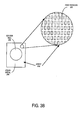
- Underlying the drain metal 216 is an array 310 of feed-throughs 230, shown in cross-section in Figure 2 .
- the drain metal 216 is formed over and connected with multiple feed-throughs 230
- the solder ball 308 is formed on the drain metal 216.
- Figure 3B represents a portion of the feed-through array 310.
- the surface area 320 that encompasses the source metal 212, gate metal 316, and drain metal 216 corresponds to the amount of surface area consumed by a conventional diffusion or deep sinker.
- the amount of surface area needed to accommodate the array 310 of feed-throughs 230 is substantially less than the area consumed by a sinker.
- the use of the feed-throughs 230 in place of a sinker frees up real estate in the chip that can be used for additional structures such as those shown in Figure 3A .
- a device of a given size can include more cells; conversely, for a given number of cells, the size of a power MOSFET flip chip can be reduced.
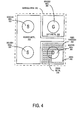
- Figure 4 shows an example of an arrangement of feed-throughs 230 in which the feed-throughs are concentrated under only a portion of the region of drain metal 216.
- the feed-throughs 230 are concentrated toward the direction from which the current is flowing - that is, toward the source region. Consequently, feed-throughs are not included in the area 410 of the drain region, further reducing the resistance of the epitaxial layer 206 ( Figure 2 ), and further reducing the amount of surface area utilized for the feed-throughs.
- the area 410 can be used for other structures, for example, to increase cell density.
- Figure 5 is a cross-sectional view of tungsten feed-throughs 510 and 512 showing selected dimensions.
- the feed-throughs 510 and 512 each have a width W of about 0.9 microns (more precisely, 0.95 microns); a depth D1 of about 8.7 microns (more precisely, 8.73 microns) measured at the shortest (shallowest) point (along the centerline) and a depth D2 of about 9.3 microns (more precisely, 9.31 microns) measured at the longest (deepest) point; and a distance (pitch P) between adjacent feed-throughs of about 1.7 microns (more precisely, 1.74 microns).
- the resistance of an array of tungsten feed-throughs is about one-half of the resistance associated with a conventional sinker.
- Figure 6 illustrates a flowchart 600 of one embodiment of a process that is used in the fabrication of semiconductor devices such as the device 200 of Figure 2 .
- specific steps are disclosed in Figure 6 , such steps are only examples. That is, embodiments according to the present invention are well suited to performing various other steps or variations of the steps recited in Figure 6 .
- the epitaxial layer 206 ( Figure 2 ) may include structures, layers, and regions not shown in the figures - those structures, layers, and regions can be formed before, during (e.g., as part of), and/or after the steps in flowchart 600 are performed.
- a first mask with openings corresponding to the locations of the source contacts 220, is applied to the upper surface of the epitaxial layer 206.
- the trenches for the source contacts are etched through those openings, and then the first mask is removed.
- the trenches for the source contacts extend partially into but not completely through the epitaxial layer 206.
- a second mask with openings corresponding to the locations of the feed-throughs 230, is applied to the upper surface of the epitaxial layer 206.
- the trenches for the feed-throughs are etched through those openings, and then the second mask is removed.
- the trenches for the feed-throughs extend completely through the epitaxial layer 206 and into the substrate layer 202.
- a conformal coating is applied to the surfaces of the source contact trenches and to the surfaces of the feed-through trenches.
- the conformal coating is applied to the surfaces of the source contact trenches and feed-through trenches in the same process step.
- the same material e.g., Ti and TiN
- Ti and TiN is used to coat the surfaces of the source contact trenches and the feed-through trenches.
- a filler material e.g., tungsten
- the filler material is deposited into the source contact trenches and the feed-through trenches in the same process step.
- the filler material is etched back so that is flush, or nearly flush, with the upper surface of the epitaxial layer 206.
- other structures can be formed.
- aluminum metal can be deposited and patterned to form source, drain, and gate regions. Subsequently, solder balls are positioned on the source, drain, and gate regions.
- the steps of i) applying the mask associated with the feed-through trenches and ii) forming the feed-through trenches are added, but the conventional steps of i) applying a mask to form a sinker and ii) forming the sinker are eliminated.
- the feed-through trenches are coated and filled at the same time that the source contact trenches are coated and filled, those steps do not lengthen the fabrication process by a significant amount, if at all.
- the feed-throughs 230 take less time to fabricate relative to the time needed to form a conventional sinker. Consequently, in total, the introduction of the feed-throughs shortens the length of the fabrication process, increasing throughput and decreasing cost.
- the feed-throughs occupy less surface area and result in lower parasitic resistance in the epitaxial layer in comparison to conventional sinkers. Consequently, the size of each cell can be decreased, thereby increasing cell density. Moreover, the device's on-resistance is reduced.
Landscapes
- Electrodes Of Semiconductors (AREA)
- Insulated Gate Type Field-Effect Transistor (AREA)
- Engineering & Computer Science (AREA)
- Manufacturing & Machinery (AREA)
- Wire Bonding (AREA)
- Internal Circuitry In Semiconductor Integrated Circuit Devices (AREA)
- Element Separation (AREA)
Applications Claiming Priority (3)
| Application Number | Priority Date | Filing Date | Title |
|---|---|---|---|
| US12/610,148 US9306056B2 (en) | 2009-10-30 | 2009-10-30 | Semiconductor device with trench-like feed-throughs |
| PCT/US2010/054877 WO2011053880A2 (en) | 2009-10-30 | 2010-10-29 | Semiconductor device |
| EP10827586.8A EP2494590B1 (de) | 2009-10-30 | 2010-10-29 | Halbleiterbauelement |
Related Parent Applications (2)
| Application Number | Title | Priority Date | Filing Date |
|---|---|---|---|
| EP10827586.8A Division EP2494590B1 (de) | 2009-10-30 | 2010-10-29 | Halbleiterbauelement |
| EP10827586.8A Division-Into EP2494590B1 (de) | 2009-10-30 | 2010-10-29 | Halbleiterbauelement |
Publications (2)
| Publication Number | Publication Date |
|---|---|
| EP2802013A1 true EP2802013A1 (de) | 2014-11-12 |
| EP2802013B1 EP2802013B1 (de) | 2019-06-12 |
Family
ID=43923034
Family Applications (2)
| Application Number | Title | Priority Date | Filing Date |
|---|---|---|---|
| EP14173340.2A Active EP2802013B1 (de) | 2009-10-30 | 2010-10-29 | Halbleiterbauelement |
| EP10827586.8A Active EP2494590B1 (de) | 2009-10-30 | 2010-10-29 | Halbleiterbauelement |
Family Applications After (1)
| Application Number | Title | Priority Date | Filing Date |
|---|---|---|---|
| EP10827586.8A Active EP2494590B1 (de) | 2009-10-30 | 2010-10-29 | Halbleiterbauelement |
Country Status (6)
| Country | Link |
|---|---|
| US (2) | US9306056B2 (de) |
| EP (2) | EP2802013B1 (de) |
| JP (2) | JP2013509729A (de) |
| KR (1) | KR101659853B1 (de) |
| CN (1) | CN102648517B (de) |
| WO (1) | WO2011053880A2 (de) |
Cited By (1)
| Publication number | Priority date | Publication date | Assignee | Title |
|---|---|---|---|---|
| CN105826366A (zh) * | 2015-01-27 | 2016-08-03 | 恩智浦有限公司 | 半导体器件 |
Families Citing this family (4)
| Publication number | Priority date | Publication date | Assignee | Title |
|---|---|---|---|---|
| US9306056B2 (en) | 2009-10-30 | 2016-04-05 | Vishay-Siliconix | Semiconductor device with trench-like feed-throughs |
| JP6131114B2 (ja) * | 2013-06-13 | 2017-05-17 | ルネサスエレクトロニクス株式会社 | 半導体装置及びその製造方法 |
| CN106233454A (zh) * | 2014-05-01 | 2016-12-14 | 松下知识产权经营株式会社 | 半导体装置及半导体模组 |
| JP7101085B2 (ja) | 2018-08-30 | 2022-07-14 | 株式会社東芝 | 半導体装置及び半導体装置の製造方法 |
Citations (6)
| Publication number | Priority date | Publication date | Assignee | Title |
|---|---|---|---|---|
| WO2001059842A1 (en) * | 2000-02-10 | 2001-08-16 | International Rectifier Corporation | Vertical conduction flip-chip device with bump contacts on single surface |
| WO2003096428A1 (en) * | 2002-05-13 | 2003-11-20 | General Semiconductor, Inc. | Trench dmos transistor structure |
| US20060273380A1 (en) * | 2005-06-06 | 2006-12-07 | M-Mos Sdn.Bhd. | Source contact and metal scheme for high density trench MOSFET |
| EP1793426A2 (de) * | 2005-11-30 | 2007-06-06 | Sharp Kabushiki Kaisha | Halbleiteranordnung mit Durchkontaktierung und Verfahren zu deren Herstellung |
| US20080237852A1 (en) * | 2007-03-30 | 2008-10-02 | Sanyo Electric Co., Ltd. | Semiconductor device |
| WO2008126914A1 (ja) * | 2007-04-06 | 2008-10-23 | Sanyo Electric Co., Ltd. | 電極構造及び半導体装置 |
Family Cites Families (125)
| Publication number | Priority date | Publication date | Assignee | Title |
|---|---|---|---|---|
| JPS57206073A (en) | 1981-06-12 | 1982-12-17 | Hitachi Ltd | Mis semiconductor device |
| NL8302092A (nl) | 1983-06-13 | 1985-01-02 | Philips Nv | Halfgeleiderinrichting bevattende een veldeffekttransistor. |
| JPH0612828B2 (ja) | 1983-06-30 | 1994-02-16 | 株式会社東芝 | 半導体装置 |
| JPS6056748U (ja) | 1983-09-22 | 1985-04-20 | 関西熱化学株式会社 | コ−クス炉均し口の内面掃除装置 |
| JPS60136378A (ja) | 1983-12-26 | 1985-07-19 | Hitachi Ltd | 半導体装置およびその製造方法 |
| US4837606A (en) | 1984-02-22 | 1989-06-06 | General Electric Company | Vertical MOSFET with reduced bipolar effects |
| JPS60196974A (ja) | 1984-03-19 | 1985-10-05 | Toshiba Corp | 導電変調型mosfet |
| GB2165090A (en) | 1984-09-26 | 1986-04-03 | Philips Electronic Associated | Improving the field distribution in high voltage semiconductor devices |
| JPS6239069A (ja) | 1985-08-13 | 1987-02-20 | Mitsubishi Electric Corp | 電界効果型半導体装置 |
| DE3689680T2 (de) | 1985-09-30 | 1994-06-23 | Toshiba Kawasaki Kk | Mittels Steuerelektrode abschaltbarer Thyristor mit unabhängigen Zünd-/Lösch-Kontrolltransistoren. |
| US4779123A (en) | 1985-12-13 | 1988-10-18 | Siliconix Incorporated | Insulated gate transistor array |
| IT1204243B (it) | 1986-03-06 | 1989-03-01 | Sgs Microelettronica Spa | Procedimento autoallineato per la fabbricazione di celle dmos di piccole dimensioni e dispositivi mos ottenuti mediante detto procedimento |
| IT1213411B (it) | 1986-12-17 | 1989-12-20 | Sgs Microelettronica Spa | Struttura mos di potenza con dispositivo di protezione contro le sovratensioni e processo per lasua fabbricazione. |
| US4775879A (en) | 1987-03-18 | 1988-10-04 | Motorola Inc. | FET structure arrangement having low on resistance |
| JPS63252480A (ja) | 1987-04-09 | 1988-10-19 | Mitsubishi Electric Corp | 縦形モス電界効果トランジスタ |
| US5283201A (en) | 1988-05-17 | 1994-02-01 | Advanced Power Technology, Inc. | High density power device fabrication process |
| US5072266A (en) | 1988-12-27 | 1991-12-10 | Siliconix Incorporated | Trench DMOS power transistor with field-shaping body profile and three-dimensional geometry |
| DE69029180T2 (de) | 1989-08-30 | 1997-05-22 | Siliconix Inc | Transistor mit Spannungsbegrenzungsanordnung |
| US5326711A (en) | 1993-01-04 | 1994-07-05 | Texas Instruments Incorporated | High performance high voltage vertical transistor and method of fabrication |
| US5410170A (en) | 1993-04-14 | 1995-04-25 | Siliconix Incorporated | DMOS power transistors with reduced number of contacts using integrated body-source connections |
| JPH07122749A (ja) | 1993-09-01 | 1995-05-12 | Toshiba Corp | 半導体装置及びその製造方法 |
| DE69330603T2 (de) | 1993-09-30 | 2002-07-04 | Consorzio Per La Ricerca Sulla Microelettronica Nel Mezzogiorno, Catania | Verfahren zur Metallisierung und Verbindung bei der Herstellung von Leistungshalbleiterbauelementen |
| JP2564786B2 (ja) | 1993-11-30 | 1996-12-18 | 日本電気株式会社 | 半導体装置およびその製造方法 |
| JP3338178B2 (ja) | 1994-05-30 | 2002-10-28 | 株式会社東芝 | 半導体装置およびその製造方法 |
| JP3104534B2 (ja) | 1994-06-27 | 2000-10-30 | ヤマハ株式会社 | 半導体装置とその製法 |
| JP3341496B2 (ja) * | 1994-11-07 | 2002-11-05 | ソニー株式会社 | 多層配線構造 |
| JP3291958B2 (ja) | 1995-02-21 | 2002-06-17 | 富士電機株式会社 | バックソースmosfet |
| TW290731B (de) | 1995-03-30 | 1996-11-11 | Siemens Ag | |
| US6049108A (en) | 1995-06-02 | 2000-04-11 | Siliconix Incorporated | Trench-gated MOSFET with bidirectional voltage clamping |
| JP3850054B2 (ja) | 1995-07-19 | 2006-11-29 | 三菱電機株式会社 | 半導体装置 |
| US5539255A (en) | 1995-09-07 | 1996-07-23 | International Business Machines Corporation | Semiconductor structure having self-aligned interconnection metallization formed from a single layer of metal |
| US6133587A (en) | 1996-01-23 | 2000-10-17 | Denso Corporation | Silicon carbide semiconductor device and process for manufacturing same |
| US5742076A (en) | 1996-06-05 | 1998-04-21 | North Carolina State University | Silicon carbide switching devices having near ideal breakdown voltage capability and ultralow on-state resistance |
| WO1998004004A1 (en) | 1996-07-19 | 1998-01-29 | Siliconix Incorporated | High density trench dmos transistor with trench bottom implant |
| JP3725266B2 (ja) | 1996-11-07 | 2005-12-07 | 株式会社半導体エネルギー研究所 | 配線形成方法 |
| JPH10172969A (ja) | 1996-12-06 | 1998-06-26 | Nec Corp | 半導体装置の製造方法 |
| TW468253B (en) | 1997-01-13 | 2001-12-11 | Hitachi Ltd | Semiconductor memory device |
| US6057558A (en) | 1997-03-05 | 2000-05-02 | Denson Corporation | Silicon carbide semiconductor device and manufacturing method thereof |
| US5899738A (en) | 1997-05-23 | 1999-05-04 | Taiwan Semiconductor Manufacturing Company, Ltd. | Method for making metal plugs in stacked vias for multilevel interconnections and contact openings while retaining the alignment marks without requiring extra masking steps |
| US6346438B1 (en) | 1997-06-30 | 2002-02-12 | Kabushiki Kaisha Toshiba | Method of manufacturing a semiconductor device |
| US6175154B1 (en) | 1997-12-16 | 2001-01-16 | Texas Instruments Incorporated | Fully encapsulated metal leads for multi-level metallization |
| US20010003367A1 (en) | 1998-06-12 | 2001-06-14 | Fwu-Iuan Hshieh | Trenched dmos device with low gate charges |
| US6329282B1 (en) | 1998-09-11 | 2001-12-11 | Texas Instruments Incorporated | Method of improving the texture of aluminum metallization for tungsten etch back processing |
| KR100284905B1 (ko) | 1998-10-16 | 2001-04-02 | 윤종용 | 반도체 장치의 콘택 형성 방법 |
| US5998833A (en) | 1998-10-26 | 1999-12-07 | North Carolina State University | Power semiconductor devices having improved high frequency switching and breakdown characteristics |
| US6621121B2 (en) | 1998-10-26 | 2003-09-16 | Silicon Semiconductor Corporation | Vertical MOSFETs having trench-based gate electrodes within deeper trench-based source electrodes |
| US6413822B2 (en) | 1999-04-22 | 2002-07-02 | Advanced Analogic Technologies, Inc. | Super-self-aligned fabrication process of trench-gate DMOS with overlying device layer |
| US6476456B1 (en) | 1999-06-10 | 2002-11-05 | International Rectifier Corporation | Integrated radiation hardened power mosgated device and schottky diode |
| GB9916868D0 (en) | 1999-07-20 | 1999-09-22 | Koninkl Philips Electronics Nv | Trench-gate field-effect transistors and their manufacture |
| US6211018B1 (en) | 1999-08-14 | 2001-04-03 | Electronics And Telecommunications Research Institute | Method for fabricating high density trench gate type power device |
| JP2001085685A (ja) | 1999-09-13 | 2001-03-30 | Shindengen Electric Mfg Co Ltd | トランジスタ |
| JP2001094094A (ja) | 1999-09-21 | 2001-04-06 | Hitachi Ltd | 半導体装置およびその製造方法 |
| US7186609B2 (en) | 1999-12-30 | 2007-03-06 | Siliconix Incorporated | Method of fabricating trench junction barrier rectifier |
| US6407435B1 (en) | 2000-02-11 | 2002-06-18 | Sharp Laboratories Of America, Inc. | Multilayer dielectric stack and method |
| US6246090B1 (en) | 2000-03-14 | 2001-06-12 | Intersil Corporation | Power trench transistor device source region formation using silicon spacer |
| JP3910335B2 (ja) | 2000-03-22 | 2007-04-25 | セイコーインスツル株式会社 | 縦形mosトランジスタ及びその製造方法 |
| GB0010041D0 (en) | 2000-04-26 | 2000-06-14 | Koninkl Philips Electronics Nv | Trench semiconductor device manufacture |
| EP1170803A3 (de) | 2000-06-08 | 2002-10-09 | Siliconix Incorporated | MOSFET mit Graben-Gateelektrode und Verfahren zu dessen Herstellung |
| US6872668B1 (en) | 2000-09-26 | 2005-03-29 | Integrated Device Technology, Inc. | Multi-step tungsten etchback process to preserve barrier integrity in an integrated circuit structure |
| DE10056871B4 (de) | 2000-11-16 | 2007-07-12 | Advanced Micro Devices, Inc., Sunnyvale | Feldeffekttransistor mit verbessertem Gatekontakt und Verfahren zur Herstellung desselben |
| US6649975B2 (en) | 2000-11-16 | 2003-11-18 | Silicon Semiconductor Corporation | Vertical power devices having trench-based electrodes therein |
| US6552389B2 (en) | 2000-12-14 | 2003-04-22 | Kabushiki Kaisha Toshiba | Offset-gate-type semiconductor device |
| KR100375230B1 (ko) | 2000-12-20 | 2003-03-08 | 삼성전자주식회사 | 매끄러운 텅스텐 표면을 갖는 반도체 장치의 배선 제조방법 |
| JP2002270840A (ja) | 2001-03-09 | 2002-09-20 | Toshiba Corp | パワーmosfet |
| JP4852792B2 (ja) | 2001-03-30 | 2012-01-11 | 株式会社デンソー | 半導体装置の製造方法 |
| JP2002353452A (ja) * | 2001-05-25 | 2002-12-06 | Toshiba Corp | 電力用半導体素子 |
| JP4421144B2 (ja) | 2001-06-29 | 2010-02-24 | 株式会社東芝 | 半導体装置 |
| US6569738B2 (en) | 2001-07-03 | 2003-05-27 | Siliconix, Inc. | Process for manufacturing trench gated MOSFET having drain/drift region |
| US6882000B2 (en) | 2001-08-10 | 2005-04-19 | Siliconix Incorporated | Trench MIS device with reduced gate-to-drain capacitance |
| US6894397B2 (en) | 2001-10-03 | 2005-05-17 | International Rectifier Corporation | Plural semiconductor devices in monolithic flip chip |
| US6657255B2 (en) | 2001-10-30 | 2003-12-02 | General Semiconductor, Inc. | Trench DMOS device with improved drain contact |
| JP2003289075A (ja) | 2002-01-22 | 2003-10-10 | Elpida Memory Inc | 半導体装置及びその製造方法 |
| US7067920B2 (en) | 2002-01-22 | 2006-06-27 | Elpida Memory, Inc. | Semiconductor device and method of fabricating the same |
| DE10212144B4 (de) | 2002-03-19 | 2005-10-06 | Infineon Technologies Ag | Transistoranordnung mit einer Struktur zur elektrischen Kontaktierung von Elektroden einer Trench-Transistorzelle |
| US6838722B2 (en) | 2002-03-22 | 2005-01-04 | Siliconix Incorporated | Structures of and methods of fabricating trench-gated MIS devices |
| JP4004843B2 (ja) | 2002-04-24 | 2007-11-07 | Necエレクトロニクス株式会社 | 縦型mosfetの製造方法 |
| KR100564605B1 (ko) | 2004-01-14 | 2006-03-28 | 삼성전자주식회사 | 반도체 소자의 금속 배선 형성 방법 |
| US6746954B2 (en) | 2002-07-02 | 2004-06-08 | Taiwan Semiconductor Manufacturing Co., Ltd. | Method of reworking tungsten particle contaminated semiconductor wafers |
| DE10239310B4 (de) | 2002-08-27 | 2005-11-03 | Infineon Technologies Ag | Verfahren zur Herstellung einer elektrisch leitenden Verbindung zwischen einer ersten und einer zweiten vergrabenen Halbleiterschicht |
| US7576388B1 (en) | 2002-10-03 | 2009-08-18 | Fairchild Semiconductor Corporation | Trench-gate LDMOS structures |
| US6919248B2 (en) | 2003-03-14 | 2005-07-19 | International Rectifier Corporation | Angled implant for shorter trench emitter |
| JP3964819B2 (ja) | 2003-04-07 | 2007-08-22 | 株式会社東芝 | 絶縁ゲート型半導体装置 |
| US6974750B2 (en) | 2003-06-11 | 2005-12-13 | International Rectifier Corporation | Process for forming a trench power MOS device suitable for large diameter wafers |
| JP3703816B2 (ja) | 2003-06-18 | 2005-10-05 | 株式会社東芝 | 半導体装置 |
| US7008871B2 (en) | 2003-07-03 | 2006-03-07 | International Business Machines Corporation | Selective capping of copper wiring |
| US7138690B2 (en) | 2003-07-21 | 2006-11-21 | Agere Systems Inc. | Shielding structure for use in a metal-oxide-semiconductor device |
| US6987052B2 (en) | 2003-10-30 | 2006-01-17 | Agere Systems Inc. | Method for making enhanced substrate contact for a semiconductor device |
| US7279743B2 (en) | 2003-12-02 | 2007-10-09 | Vishay-Siliconix | Closed cell trench metal-oxide-semiconductor field effect transistor |
| JP4829473B2 (ja) | 2004-01-21 | 2011-12-07 | オンセミコンダクター・トレーディング・リミテッド | 絶縁ゲート型半導体装置およびその製造方法 |
| JP2005243664A (ja) | 2004-02-24 | 2005-09-08 | Renesas Technology Corp | 半導体装置およびその製造方法 |
| US20050199918A1 (en) | 2004-03-15 | 2005-09-15 | Daniel Calafut | Optimized trench power MOSFET with integrated schottky diode |
| US6906380B1 (en) | 2004-05-13 | 2005-06-14 | Vishay-Siliconix | Drain side gate trench metal-oxide-semiconductor field effect transistor |
| US8183629B2 (en) | 2004-05-13 | 2012-05-22 | Vishay-Siliconix | Stacked trench metal-oxide-semiconductor field effect transistor device |
| US7061057B2 (en) | 2004-06-16 | 2006-06-13 | Cree Microwave, Llc | Laterally diffused MOS transistor having N+ source contact to N-doped substrate |
| US20050280085A1 (en) | 2004-06-16 | 2005-12-22 | Cree Microwave, Inc. | LDMOS transistor having gate shield and trench source capacitor |
| JP2006012967A (ja) | 2004-06-23 | 2006-01-12 | Toshiba Corp | 半導体装置 |
| US7352036B2 (en) * | 2004-08-03 | 2008-04-01 | Fairchild Semiconductor Corporation | Semiconductor power device having a top-side drain using a sinker trench |
| US7439580B2 (en) | 2004-09-02 | 2008-10-21 | International Rectifier Corporation | Top drain MOSgated device and process of manufacture therefor |
| JP4153932B2 (ja) * | 2004-09-24 | 2008-09-24 | 株式会社東芝 | 半導体装置および半導体装置の製造方法 |
| JP2006286953A (ja) | 2005-03-31 | 2006-10-19 | Eudyna Devices Inc | 半導体装置およびその製造方法 |
| US7535057B2 (en) | 2005-05-24 | 2009-05-19 | Robert Kuo-Chang Yang | DMOS transistor with a poly-filled deep trench for improved performance |
| US20060273390A1 (en) | 2005-06-06 | 2006-12-07 | M-Mos Sdn. Bhd. | Gate contact and runners for high density trench MOSFET |
| US20060273382A1 (en) * | 2005-06-06 | 2006-12-07 | M-Mos Sdn. Bhd. | High density trench MOSFET with low gate resistance and reduced source contact space |
| JP4452217B2 (ja) * | 2005-07-04 | 2010-04-21 | 富士通マイクロエレクトロニクス株式会社 | 半導体装置 |
| US7282765B2 (en) | 2005-07-13 | 2007-10-16 | Ciclon Semiconductor Device Corp. | Power LDMOS transistor |
| US7385248B2 (en) | 2005-08-09 | 2008-06-10 | Fairchild Semiconductor Corporation | Shielded gate field effect transistor with improved inter-poly dielectric |
| US7235845B2 (en) | 2005-08-12 | 2007-06-26 | Ciclon Semiconductor Device Corp. | Power LDMOS transistor |
| JP2007142272A (ja) * | 2005-11-21 | 2007-06-07 | Sanyo Electric Co Ltd | 半導体装置 |
| US7687851B2 (en) | 2005-11-23 | 2010-03-30 | M-Mos Semiconductor Sdn. Bhd. | High density trench MOSFET with reduced on-resistance |
| JP2007184553A (ja) | 2005-12-06 | 2007-07-19 | Sanyo Electric Co Ltd | 半導体装置及びその製造方法 |
| US7544545B2 (en) | 2005-12-28 | 2009-06-09 | Vishay-Siliconix | Trench polysilicon diode |
| US7586147B2 (en) | 2006-04-17 | 2009-09-08 | Taiwan Semiconductor Manufacturing Co. Ltd. | Butted source contact and well strap |
| US8471390B2 (en) | 2006-05-12 | 2013-06-25 | Vishay-Siliconix | Power MOSFET contact metallization |
| US8008716B2 (en) * | 2006-09-17 | 2011-08-30 | Alpha & Omega Semiconductor, Ltd | Inverted-trench grounded-source FET structure with trenched source body short electrode |
| US7468536B2 (en) | 2007-02-16 | 2008-12-23 | Power Integrations, Inc. | Gate metal routing for transistor with checkerboarded layout |
| US7952145B2 (en) | 2007-02-20 | 2011-05-31 | Texas Instruments Lehigh Valley Incorporated | MOS transistor device in common source configuration |
| US8368126B2 (en) | 2007-04-19 | 2013-02-05 | Vishay-Siliconix | Trench metal oxide semiconductor with recessed trench material and remote contacts |
| JP5132977B2 (ja) | 2007-04-26 | 2013-01-30 | ルネサスエレクトロニクス株式会社 | 半導体装置およびその製造方法 |
| US8035159B2 (en) | 2007-04-30 | 2011-10-11 | Alpha & Omega Semiconductor, Ltd. | Device structure and manufacturing method using HDP deposited source-body implant block |
| CN101868856B (zh) | 2007-09-21 | 2014-03-12 | 飞兆半导体公司 | 用于功率器件的超结结构及制造方法 |
| US7550803B1 (en) | 2008-04-15 | 2009-06-23 | United Microelectronics Corp. | Vertical double-diffusion metal-oxide-semiconductor transistor device |
| US7781832B2 (en) | 2008-05-28 | 2010-08-24 | Ptek Technology Co., Ltd. | Trench-type power MOS transistor and integrated circuit utilizing the same |
| TWI396240B (zh) * | 2009-05-08 | 2013-05-11 | 茂達電子股份有限公司 | 製造功率半導體元件的方法 |
| US9306056B2 (en) | 2009-10-30 | 2016-04-05 | Vishay-Siliconix | Semiconductor device with trench-like feed-throughs |
| US8604525B2 (en) | 2009-11-02 | 2013-12-10 | Vishay-Siliconix | Transistor structure with feed-through source-to-substrate contact |
-
2009
- 2009-10-30 US US12/610,148 patent/US9306056B2/en active Active
-
2010
- 2010-10-29 WO PCT/US2010/054877 patent/WO2011053880A2/en not_active Ceased
- 2010-10-29 EP EP14173340.2A patent/EP2802013B1/de active Active
- 2010-10-29 EP EP10827586.8A patent/EP2494590B1/de active Active
- 2010-10-29 JP JP2012537156A patent/JP2013509729A/ja active Pending
- 2010-10-29 CN CN201080056535.0A patent/CN102648517B/zh active Active
- 2010-10-29 KR KR1020127010451A patent/KR101659853B1/ko active Active
-
2015
- 2015-02-17 JP JP2015028533A patent/JP6130415B2/ja active Active
-
2016
- 2016-04-05 US US15/091,431 patent/US10032901B2/en active Active
Patent Citations (7)
| Publication number | Priority date | Publication date | Assignee | Title |
|---|---|---|---|---|
| WO2001059842A1 (en) * | 2000-02-10 | 2001-08-16 | International Rectifier Corporation | Vertical conduction flip-chip device with bump contacts on single surface |
| WO2003096428A1 (en) * | 2002-05-13 | 2003-11-20 | General Semiconductor, Inc. | Trench dmos transistor structure |
| US20060273380A1 (en) * | 2005-06-06 | 2006-12-07 | M-Mos Sdn.Bhd. | Source contact and metal scheme for high density trench MOSFET |
| EP1793426A2 (de) * | 2005-11-30 | 2007-06-06 | Sharp Kabushiki Kaisha | Halbleiteranordnung mit Durchkontaktierung und Verfahren zu deren Herstellung |
| US20080237852A1 (en) * | 2007-03-30 | 2008-10-02 | Sanyo Electric Co., Ltd. | Semiconductor device |
| WO2008126914A1 (ja) * | 2007-04-06 | 2008-10-23 | Sanyo Electric Co., Ltd. | 電極構造及び半導体装置 |
| US20090315175A1 (en) * | 2007-04-06 | 2009-12-24 | Sanyo Electric Co., Ltd. | Electrode structure and semiconductor device |
Cited By (4)
| Publication number | Priority date | Publication date | Assignee | Title |
|---|---|---|---|---|
| CN105826366A (zh) * | 2015-01-27 | 2016-08-03 | 恩智浦有限公司 | 半导体器件 |
| EP3051592A1 (de) * | 2015-01-27 | 2016-08-03 | Nxp B.V. | Halbleiterbauelement |
| CN105826366B (zh) * | 2015-01-27 | 2019-03-22 | 安世有限公司 | 半导体器件 |
| US10643941B2 (en) | 2015-01-27 | 2020-05-05 | Nexperia B.V. | Semiconductor device |
Also Published As
| Publication number | Publication date |
|---|---|
| US20170025527A1 (en) | 2017-01-26 |
| JP2015130516A (ja) | 2015-07-16 |
| KR101659853B1 (ko) | 2016-09-30 |
| US10032901B2 (en) | 2018-07-24 |
| EP2494590A4 (de) | 2013-04-24 |
| US9306056B2 (en) | 2016-04-05 |
| JP6130415B2 (ja) | 2017-05-17 |
| EP2494590A2 (de) | 2012-09-05 |
| CN102648517A (zh) | 2012-08-22 |
| CN102648517B (zh) | 2016-02-03 |
| EP2494590B1 (de) | 2017-07-19 |
| JP2013509729A (ja) | 2013-03-14 |
| WO2011053880A3 (en) | 2011-08-04 |
| EP2802013B1 (de) | 2019-06-12 |
| WO2011053880A2 (en) | 2011-05-05 |
| US20110101525A1 (en) | 2011-05-05 |
| KR20120118455A (ko) | 2012-10-26 |
Similar Documents
| Publication | Publication Date | Title |
|---|---|---|
| US8653587B2 (en) | Trench MOSFET having a top side drain | |
| US9443974B2 (en) | Super junction trench power MOSFET device fabrication | |
| US9425306B2 (en) | Super junction trench power MOSFET devices | |
| TWI466293B (zh) | 具有金屬閘極堆疊之積體電路與其形成方法 | |
| US20150162448A1 (en) | Integrated circuit device with power gating switch in back end of line | |
| US10032901B2 (en) | Semiconductor device with trench-like feed-throughs | |
| US8338907B2 (en) | Semiconductor device and method of manufacturing the same | |
| US8445958B2 (en) | Power semiconductor device with trench bottom polysilicon and fabrication method thereof | |
| US7687352B2 (en) | Trench MOSFET and method of manufacture utilizing four masks | |
| KR20070044481A (ko) | 싱커 트렌치를 사용하는 상부 드레인을 구비한 전력 반도체장치 | |
| JP2013508981A (ja) | 超高密度パワートレンチmosfet | |
| US9171950B2 (en) | Semiconductor component and method for producing a semiconductor component | |
| US8159025B2 (en) | Gate electrode in a trench for power MOS transistors | |
| US7714382B2 (en) | Trench gate semiconductor with NPN junctions beneath shallow trench isolation structures | |
| US7659597B2 (en) | Integrated circuit wire patterns including integral plug portions | |
| US20240304680A1 (en) | Method of manufacturing semiconductor device | |
| US7439581B2 (en) | Transistors, semiconductor integrated circuit interconnections and methods of forming the same | |
| CN121751745A (zh) | 具有垂直晶体管器件的半导体管芯 | |
| CN106784002A (zh) | 一种制造n沟道增强型mos晶体管器件的方法 |
Legal Events
| Date | Code | Title | Description |
|---|---|---|---|
| PUAI | Public reference made under article 153(3) epc to a published international application that has entered the european phase |
Free format text: ORIGINAL CODE: 0009012 |
|
| 17P | Request for examination filed |
Effective date: 20140715 |
|
| AC | Divisional application: reference to earlier application |
Ref document number: 2494590 Country of ref document: EP Kind code of ref document: P |
|
| AK | Designated contracting states |
Kind code of ref document: A1 Designated state(s): AL AT BE BG CH CY CZ DE DK EE ES FI FR GB GR HR HU IE IS IT LI LT LU LV MC MK MT NL NO PL PT RO RS SE SI SK SM TR |
|
| STAA | Information on the status of an ep patent application or granted ep patent |
Free format text: STATUS: EXAMINATION IS IN PROGRESS |
|
| 17Q | First examination report despatched |
Effective date: 20171006 |
|
| GRAP | Despatch of communication of intention to grant a patent |
Free format text: ORIGINAL CODE: EPIDOSNIGR1 |
|
| STAA | Information on the status of an ep patent application or granted ep patent |
Free format text: STATUS: GRANT OF PATENT IS INTENDED |
|
| RIC1 | Information provided on ipc code assigned before grant |
Ipc: H01L 29/78 20060101AFI20180716BHEP Ipc: H01L 29/417 20060101ALI20180716BHEP Ipc: H01L 23/485 20060101ALI20180716BHEP |
|
| INTG | Intention to grant announced |
Effective date: 20180814 |
|
| GRAJ | Information related to disapproval of communication of intention to grant by the applicant or resumption of examination proceedings by the epo deleted |
Free format text: ORIGINAL CODE: EPIDOSDIGR1 |
|
| STAA | Information on the status of an ep patent application or granted ep patent |
Free format text: STATUS: EXAMINATION IS IN PROGRESS |
|
| GRAP | Despatch of communication of intention to grant a patent |
Free format text: ORIGINAL CODE: EPIDOSNIGR1 |
|
| STAA | Information on the status of an ep patent application or granted ep patent |
Free format text: STATUS: GRANT OF PATENT IS INTENDED |
|
| INTC | Intention to grant announced (deleted) | ||
| INTG | Intention to grant announced |
Effective date: 20190108 |
|
| GRAS | Grant fee paid |
Free format text: ORIGINAL CODE: EPIDOSNIGR3 |
|
| GRAA | (expected) grant |
Free format text: ORIGINAL CODE: 0009210 |
|
| STAA | Information on the status of an ep patent application or granted ep patent |
Free format text: STATUS: THE PATENT HAS BEEN GRANTED |
|
| AC | Divisional application: reference to earlier application |
Ref document number: 2494590 Country of ref document: EP Kind code of ref document: P |
|
| AK | Designated contracting states |
Kind code of ref document: B1 Designated state(s): AL AT BE BG CH CY CZ DE DK EE ES FI FR GB GR HR HU IE IS IT LI LT LU LV MC MK MT NL NO PL PT RO RS SE SI SK SM TR |
|
| REG | Reference to a national code |
Ref country code: GB Ref legal event code: FG4D |
|
| REG | Reference to a national code |
Ref country code: CH Ref legal event code: EP |
|
| REG | Reference to a national code |
Ref country code: AT Ref legal event code: REF Ref document number: 1143715 Country of ref document: AT Kind code of ref document: T Effective date: 20190615 |
|
| REG | Reference to a national code |
Ref country code: DE Ref legal event code: R096 Ref document number: 602010059474 Country of ref document: DE |
|
| REG | Reference to a national code |
Ref country code: IE Ref legal event code: FG4D |
|
| REG | Reference to a national code |
Ref country code: NL Ref legal event code: MP Effective date: 20190612 |
|
| REG | Reference to a national code |
Ref country code: LT Ref legal event code: MG4D |
|
| PG25 | Lapsed in a contracting state [announced via postgrant information from national office to epo] |
Ref country code: HR Free format text: LAPSE BECAUSE OF FAILURE TO SUBMIT A TRANSLATION OF THE DESCRIPTION OR TO PAY THE FEE WITHIN THE PRESCRIBED TIME-LIMIT Effective date: 20190612 Ref country code: SE Free format text: LAPSE BECAUSE OF FAILURE TO SUBMIT A TRANSLATION OF THE DESCRIPTION OR TO PAY THE FEE WITHIN THE PRESCRIBED TIME-LIMIT Effective date: 20190612 Ref country code: LT Free format text: LAPSE BECAUSE OF FAILURE TO SUBMIT A TRANSLATION OF THE DESCRIPTION OR TO PAY THE FEE WITHIN THE PRESCRIBED TIME-LIMIT Effective date: 20190612 Ref country code: NO Free format text: LAPSE BECAUSE OF FAILURE TO SUBMIT A TRANSLATION OF THE DESCRIPTION OR TO PAY THE FEE WITHIN THE PRESCRIBED TIME-LIMIT Effective date: 20190912 Ref country code: AL Free format text: LAPSE BECAUSE OF FAILURE TO SUBMIT A TRANSLATION OF THE DESCRIPTION OR TO PAY THE FEE WITHIN THE PRESCRIBED TIME-LIMIT Effective date: 20190612 Ref country code: FI Free format text: LAPSE BECAUSE OF FAILURE TO SUBMIT A TRANSLATION OF THE DESCRIPTION OR TO PAY THE FEE WITHIN THE PRESCRIBED TIME-LIMIT Effective date: 20190612 |
|
| PG25 | Lapsed in a contracting state [announced via postgrant information from national office to epo] |
Ref country code: GR Free format text: LAPSE BECAUSE OF FAILURE TO SUBMIT A TRANSLATION OF THE DESCRIPTION OR TO PAY THE FEE WITHIN THE PRESCRIBED TIME-LIMIT Effective date: 20190913 Ref country code: BG Free format text: LAPSE BECAUSE OF FAILURE TO SUBMIT A TRANSLATION OF THE DESCRIPTION OR TO PAY THE FEE WITHIN THE PRESCRIBED TIME-LIMIT Effective date: 20190912 Ref country code: RS Free format text: LAPSE BECAUSE OF FAILURE TO SUBMIT A TRANSLATION OF THE DESCRIPTION OR TO PAY THE FEE WITHIN THE PRESCRIBED TIME-LIMIT Effective date: 20190612 Ref country code: LV Free format text: LAPSE BECAUSE OF FAILURE TO SUBMIT A TRANSLATION OF THE DESCRIPTION OR TO PAY THE FEE WITHIN THE PRESCRIBED TIME-LIMIT Effective date: 20190612 |
|
| REG | Reference to a national code |
Ref country code: AT Ref legal event code: MK05 Ref document number: 1143715 Country of ref document: AT Kind code of ref document: T Effective date: 20190612 |
|
| PG25 | Lapsed in a contracting state [announced via postgrant information from national office to epo] |
Ref country code: NL Free format text: LAPSE BECAUSE OF FAILURE TO SUBMIT A TRANSLATION OF THE DESCRIPTION OR TO PAY THE FEE WITHIN THE PRESCRIBED TIME-LIMIT Effective date: 20190612 Ref country code: PT Free format text: LAPSE BECAUSE OF FAILURE TO SUBMIT A TRANSLATION OF THE DESCRIPTION OR TO PAY THE FEE WITHIN THE PRESCRIBED TIME-LIMIT Effective date: 20191014 Ref country code: SK Free format text: LAPSE BECAUSE OF FAILURE TO SUBMIT A TRANSLATION OF THE DESCRIPTION OR TO PAY THE FEE WITHIN THE PRESCRIBED TIME-LIMIT Effective date: 20190612 Ref country code: CZ Free format text: LAPSE BECAUSE OF FAILURE TO SUBMIT A TRANSLATION OF THE DESCRIPTION OR TO PAY THE FEE WITHIN THE PRESCRIBED TIME-LIMIT Effective date: 20190612 Ref country code: RO Free format text: LAPSE BECAUSE OF FAILURE TO SUBMIT A TRANSLATION OF THE DESCRIPTION OR TO PAY THE FEE WITHIN THE PRESCRIBED TIME-LIMIT Effective date: 20190612 Ref country code: EE Free format text: LAPSE BECAUSE OF FAILURE TO SUBMIT A TRANSLATION OF THE DESCRIPTION OR TO PAY THE FEE WITHIN THE PRESCRIBED TIME-LIMIT Effective date: 20190612 Ref country code: AT Free format text: LAPSE BECAUSE OF FAILURE TO SUBMIT A TRANSLATION OF THE DESCRIPTION OR TO PAY THE FEE WITHIN THE PRESCRIBED TIME-LIMIT Effective date: 20190612 |
|
| PG25 | Lapsed in a contracting state [announced via postgrant information from national office to epo] |
Ref country code: IS Free format text: LAPSE BECAUSE OF FAILURE TO SUBMIT A TRANSLATION OF THE DESCRIPTION OR TO PAY THE FEE WITHIN THE PRESCRIBED TIME-LIMIT Effective date: 20191012 Ref country code: ES Free format text: LAPSE BECAUSE OF FAILURE TO SUBMIT A TRANSLATION OF THE DESCRIPTION OR TO PAY THE FEE WITHIN THE PRESCRIBED TIME-LIMIT Effective date: 20190612 Ref country code: SM Free format text: LAPSE BECAUSE OF FAILURE TO SUBMIT A TRANSLATION OF THE DESCRIPTION OR TO PAY THE FEE WITHIN THE PRESCRIBED TIME-LIMIT Effective date: 20190612 Ref country code: IT Free format text: LAPSE BECAUSE OF FAILURE TO SUBMIT A TRANSLATION OF THE DESCRIPTION OR TO PAY THE FEE WITHIN THE PRESCRIBED TIME-LIMIT Effective date: 20190612 |
|
| REG | Reference to a national code |
Ref country code: DE Ref legal event code: R097 Ref document number: 602010059474 Country of ref document: DE |
|
| PG25 | Lapsed in a contracting state [announced via postgrant information from national office to epo] |
Ref country code: TR Free format text: LAPSE BECAUSE OF FAILURE TO SUBMIT A TRANSLATION OF THE DESCRIPTION OR TO PAY THE FEE WITHIN THE PRESCRIBED TIME-LIMIT Effective date: 20190612 |
|
| PLBE | No opposition filed within time limit |
Free format text: ORIGINAL CODE: 0009261 |
|
| STAA | Information on the status of an ep patent application or granted ep patent |
Free format text: STATUS: NO OPPOSITION FILED WITHIN TIME LIMIT |
|
| PG25 | Lapsed in a contracting state [announced via postgrant information from national office to epo] |
Ref country code: DK Free format text: LAPSE BECAUSE OF FAILURE TO SUBMIT A TRANSLATION OF THE DESCRIPTION OR TO PAY THE FEE WITHIN THE PRESCRIBED TIME-LIMIT Effective date: 20190612 Ref country code: PL Free format text: LAPSE BECAUSE OF FAILURE TO SUBMIT A TRANSLATION OF THE DESCRIPTION OR TO PAY THE FEE WITHIN THE PRESCRIBED TIME-LIMIT Effective date: 20190612 |
|
| 26N | No opposition filed |
Effective date: 20200313 |
|
| PG25 | Lapsed in a contracting state [announced via postgrant information from national office to epo] |
Ref country code: IS Free format text: LAPSE BECAUSE OF FAILURE TO SUBMIT A TRANSLATION OF THE DESCRIPTION OR TO PAY THE FEE WITHIN THE PRESCRIBED TIME-LIMIT Effective date: 20200224 Ref country code: SI Free format text: LAPSE BECAUSE OF FAILURE TO SUBMIT A TRANSLATION OF THE DESCRIPTION OR TO PAY THE FEE WITHIN THE PRESCRIBED TIME-LIMIT Effective date: 20190612 Ref country code: MC Free format text: LAPSE BECAUSE OF FAILURE TO SUBMIT A TRANSLATION OF THE DESCRIPTION OR TO PAY THE FEE WITHIN THE PRESCRIBED TIME-LIMIT Effective date: 20190612 |
|
| REG | Reference to a national code |
Ref country code: CH Ref legal event code: PL |
|
| PG2D | Information on lapse in contracting state deleted |
Ref country code: IS |
|
| PG25 | Lapsed in a contracting state [announced via postgrant information from national office to epo] |
Ref country code: CH Free format text: LAPSE BECAUSE OF NON-PAYMENT OF DUE FEES Effective date: 20191031 Ref country code: LU Free format text: LAPSE BECAUSE OF NON-PAYMENT OF DUE FEES Effective date: 20191029 Ref country code: LI Free format text: LAPSE BECAUSE OF NON-PAYMENT OF DUE FEES Effective date: 20191031 |
|
| REG | Reference to a national code |
Ref country code: BE Ref legal event code: MM Effective date: 20191031 |
|
| PG25 | Lapsed in a contracting state [announced via postgrant information from national office to epo] |
Ref country code: BE Free format text: LAPSE BECAUSE OF NON-PAYMENT OF DUE FEES Effective date: 20191031 |
|
| PG25 | Lapsed in a contracting state [announced via postgrant information from national office to epo] |
Ref country code: IE Free format text: LAPSE BECAUSE OF NON-PAYMENT OF DUE FEES Effective date: 20191029 |
|
| PG25 | Lapsed in a contracting state [announced via postgrant information from national office to epo] |
Ref country code: CY Free format text: LAPSE BECAUSE OF FAILURE TO SUBMIT A TRANSLATION OF THE DESCRIPTION OR TO PAY THE FEE WITHIN THE PRESCRIBED TIME-LIMIT Effective date: 20190612 |
|
| PG25 | Lapsed in a contracting state [announced via postgrant information from national office to epo] |
Ref country code: MT Free format text: LAPSE BECAUSE OF FAILURE TO SUBMIT A TRANSLATION OF THE DESCRIPTION OR TO PAY THE FEE WITHIN THE PRESCRIBED TIME-LIMIT Effective date: 20190612 Ref country code: HU Free format text: LAPSE BECAUSE OF FAILURE TO SUBMIT A TRANSLATION OF THE DESCRIPTION OR TO PAY THE FEE WITHIN THE PRESCRIBED TIME-LIMIT; INVALID AB INITIO Effective date: 20101029 |
|
| PG25 | Lapsed in a contracting state [announced via postgrant information from national office to epo] |
Ref country code: MK Free format text: LAPSE BECAUSE OF FAILURE TO SUBMIT A TRANSLATION OF THE DESCRIPTION OR TO PAY THE FEE WITHIN THE PRESCRIBED TIME-LIMIT Effective date: 20190612 |
|
| REG | Reference to a national code |
Ref country code: DE Ref legal event code: R079 Ref document number: 602010059474 Country of ref document: DE Free format text: PREVIOUS MAIN CLASS: H01L0029780000 Ipc: H10D0030600000 |
|
| PGFP | Annual fee paid to national office [announced via postgrant information from national office to epo] |
Ref country code: DE Payment date: 20251029 Year of fee payment: 16 |
|
| PGFP | Annual fee paid to national office [announced via postgrant information from national office to epo] |
Ref country code: GB Payment date: 20251027 Year of fee payment: 16 |
|
| PGFP | Annual fee paid to national office [announced via postgrant information from national office to epo] |
Ref country code: FR Payment date: 20251027 Year of fee payment: 16 |