EP2774244B2 - Energieeffiziente induktives stromübertragungssystem und verfahren dafür - Google Patents
Energieeffiziente induktives stromübertragungssystem und verfahren dafür Download PDFInfo
- Publication number
- EP2774244B2 EP2774244B2 EP11773322.0A EP11773322A EP2774244B2 EP 2774244 B2 EP2774244 B2 EP 2774244B2 EP 11773322 A EP11773322 A EP 11773322A EP 2774244 B2 EP2774244 B2 EP 2774244B2
- Authority
- EP
- European Patent Office
- Prior art keywords
- inductive
- power
- primary
- inductive power
- signal
- Prior art date
- Legal status (The legal status is an assumption and is not a legal conclusion. Google has not performed a legal analysis and makes no representation as to the accuracy of the status listed.)
- Active
Links
- 230000001939 inductive effect Effects 0.000 title claims description 314
- 230000005540 biological transmission Effects 0.000 title description 129
- 238000000034 method Methods 0.000 title description 22
- 230000004913 activation Effects 0.000 claims description 14
- 230000000977 initiatory effect Effects 0.000 claims 1
- 238000012546 transfer Methods 0.000 description 72
- 238000004891 communication Methods 0.000 description 21
- 230000001965 increasing effect Effects 0.000 description 19
- 230000007246 mechanism Effects 0.000 description 15
- 238000010586 diagram Methods 0.000 description 12
- 230000003247 decreasing effect Effects 0.000 description 9
- 230000033228 biological regulation Effects 0.000 description 7
- 238000012544 monitoring process Methods 0.000 description 7
- 230000001105 regulatory effect Effects 0.000 description 6
- 230000004044 response Effects 0.000 description 6
- 239000003990 capacitor Substances 0.000 description 5
- 230000008859 change Effects 0.000 description 5
- 230000003213 activating effect Effects 0.000 description 4
- 230000005611 electricity Effects 0.000 description 4
- 230000007613 environmental effect Effects 0.000 description 4
- 230000007704 transition Effects 0.000 description 4
- 230000008878 coupling Effects 0.000 description 3
- 238000010168 coupling process Methods 0.000 description 3
- 238000005859 coupling reaction Methods 0.000 description 3
- 238000001514 detection method Methods 0.000 description 3
- 238000010438 heat treatment Methods 0.000 description 3
- 230000003287 optical effect Effects 0.000 description 3
- 230000008569 process Effects 0.000 description 3
- 230000008054 signal transmission Effects 0.000 description 3
- CURLTUGMZLYLDI-UHFFFAOYSA-N Carbon dioxide Chemical compound O=C=O CURLTUGMZLYLDI-UHFFFAOYSA-N 0.000 description 2
- 230000005355 Hall effect Effects 0.000 description 2
- 230000009471 action Effects 0.000 description 2
- 238000013459 approach Methods 0.000 description 2
- 230000008901 benefit Effects 0.000 description 2
- 230000001419 dependent effect Effects 0.000 description 2
- 230000005670 electromagnetic radiation Effects 0.000 description 2
- 238000005265 energy consumption Methods 0.000 description 2
- 230000006870 function Effects 0.000 description 2
- 239000002184 metal Substances 0.000 description 2
- 235000014676 Phragmites communis Nutrition 0.000 description 1
- 239000012190 activator Substances 0.000 description 1
- 230000003044 adaptive effect Effects 0.000 description 1
- 238000007664 blowing Methods 0.000 description 1
- 229910002092 carbon dioxide Inorganic materials 0.000 description 1
- 239000001569 carbon dioxide Substances 0.000 description 1
- 238000010425 computer drawing Methods 0.000 description 1
- LTMHDMANZUZIPE-PUGKRICDSA-N digoxin Chemical compound C1[C@H](O)[C@H](O)[C@@H](C)O[C@H]1O[C@@H]1[C@@H](C)O[C@@H](O[C@@H]2[C@H](O[C@@H](O[C@@H]3C[C@@H]4[C@]([C@@H]5[C@H]([C@]6(CC[C@@H]([C@@]6(C)[C@H](O)C5)C=5COC(=O)C=5)O)CC4)(C)CC3)C[C@@H]2O)C)C[C@@H]1O LTMHDMANZUZIPE-PUGKRICDSA-N 0.000 description 1
- 238000006073 displacement reaction Methods 0.000 description 1
- 230000000694 effects Effects 0.000 description 1
- 230000005674 electromagnetic induction Effects 0.000 description 1
- 238000005516 engineering process Methods 0.000 description 1
- 230000007717 exclusion Effects 0.000 description 1
- 230000005669 field effect Effects 0.000 description 1
- 239000002803 fossil fuel Substances 0.000 description 1
- 239000000446 fuel Substances 0.000 description 1
- 239000005431 greenhouse gas Substances 0.000 description 1
- 230000017525 heat dissipation Effects 0.000 description 1
- 230000006698 induction Effects 0.000 description 1
- 230000002045 lasting effect Effects 0.000 description 1
- 229910044991 metal oxide Inorganic materials 0.000 description 1
- 150000004706 metal oxides Chemical class 0.000 description 1
- 238000012986 modification Methods 0.000 description 1
- 230000004048 modification Effects 0.000 description 1
- 238000013021 overheating Methods 0.000 description 1
- 230000037361 pathway Effects 0.000 description 1
- 230000000149 penetrating effect Effects 0.000 description 1
- 238000007747 plating Methods 0.000 description 1
- 239000002244 precipitate Substances 0.000 description 1
- 239000000047 product Substances 0.000 description 1
- 239000004065 semiconductor Substances 0.000 description 1
- 238000010792 warming Methods 0.000 description 1
- XLYOFNOQVPJJNP-UHFFFAOYSA-N water Substances O XLYOFNOQVPJJNP-UHFFFAOYSA-N 0.000 description 1
Images


Classifications
-
- H—ELECTRICITY
- H04—ELECTRIC COMMUNICATION TECHNIQUE
- H04B—TRANSMISSION
- H04B5/00—Near-field transmission systems, e.g. inductive or capacitive transmission systems
- H04B5/70—Near-field transmission systems, e.g. inductive or capacitive transmission systems specially adapted for specific purposes
- H04B5/79—Near-field transmission systems, e.g. inductive or capacitive transmission systems specially adapted for specific purposes for data transfer in combination with power transfer
-
- H—ELECTRICITY
- H01—ELECTRIC ELEMENTS
- H01F—MAGNETS; INDUCTANCES; TRANSFORMERS; SELECTION OF MATERIALS FOR THEIR MAGNETIC PROPERTIES
- H01F38/00—Adaptations of transformers or inductances for specific applications or functions
- H01F38/14—Inductive couplings
-
- H—ELECTRICITY
- H02—GENERATION; CONVERSION OR DISTRIBUTION OF ELECTRIC POWER
- H02J—CIRCUIT ARRANGEMENTS OR SYSTEMS FOR SUPPLYING OR DISTRIBUTING ELECTRIC POWER; SYSTEMS FOR STORING ELECTRIC ENERGY
- H02J50/00—Circuit arrangements or systems for wireless supply or distribution of electric power
- H02J50/10—Circuit arrangements or systems for wireless supply or distribution of electric power using inductive coupling
- H02J50/12—Circuit arrangements or systems for wireless supply or distribution of electric power using inductive coupling of the resonant type
-
- H—ELECTRICITY
- H02—GENERATION; CONVERSION OR DISTRIBUTION OF ELECTRIC POWER
- H02J—CIRCUIT ARRANGEMENTS OR SYSTEMS FOR SUPPLYING OR DISTRIBUTING ELECTRIC POWER; SYSTEMS FOR STORING ELECTRIC ENERGY
- H02J50/00—Circuit arrangements or systems for wireless supply or distribution of electric power
- H02J50/40—Circuit arrangements or systems for wireless supply or distribution of electric power using two or more transmitting or receiving devices
-
- H—ELECTRICITY
- H02—GENERATION; CONVERSION OR DISTRIBUTION OF ELECTRIC POWER
- H02J—CIRCUIT ARRANGEMENTS OR SYSTEMS FOR SUPPLYING OR DISTRIBUTING ELECTRIC POWER; SYSTEMS FOR STORING ELECTRIC ENERGY
- H02J50/00—Circuit arrangements or systems for wireless supply or distribution of electric power
- H02J50/80—Circuit arrangements or systems for wireless supply or distribution of electric power involving the exchange of data, concerning supply or distribution of electric power, between transmitting devices and receiving devices
-
- H—ELECTRICITY
- H02—GENERATION; CONVERSION OR DISTRIBUTION OF ELECTRIC POWER
- H02J—CIRCUIT ARRANGEMENTS OR SYSTEMS FOR SUPPLYING OR DISTRIBUTING ELECTRIC POWER; SYSTEMS FOR STORING ELECTRIC ENERGY
- H02J7/00—Circuit arrangements for charging or depolarising batteries or for supplying loads from batteries
- H02J7/00032—Circuit arrangements for charging or depolarising batteries or for supplying loads from batteries characterised by data exchange
- H02J7/00045—Authentication, i.e. circuits for checking compatibility between one component, e.g. a battery or a battery charger, and another component, e.g. a power source
-
- H—ELECTRICITY
- H02—GENERATION; CONVERSION OR DISTRIBUTION OF ELECTRIC POWER
- H02J—CIRCUIT ARRANGEMENTS OR SYSTEMS FOR SUPPLYING OR DISTRIBUTING ELECTRIC POWER; SYSTEMS FOR STORING ELECTRIC ENERGY
- H02J7/00—Circuit arrangements for charging or depolarising batteries or for supplying loads from batteries
- H02J7/0029—Circuit arrangements for charging or depolarising batteries or for supplying loads from batteries with safety or protection devices or circuits
-
- H—ELECTRICITY
- H02—GENERATION; CONVERSION OR DISTRIBUTION OF ELECTRIC POWER
- H02J—CIRCUIT ARRANGEMENTS OR SYSTEMS FOR SUPPLYING OR DISTRIBUTING ELECTRIC POWER; SYSTEMS FOR STORING ELECTRIC ENERGY
- H02J7/00—Circuit arrangements for charging or depolarising batteries or for supplying loads from batteries
- H02J7/0047—Circuit arrangements for charging or depolarising batteries or for supplying loads from batteries with monitoring or indicating devices or circuits
-
- H—ELECTRICITY
- H04—ELECTRIC COMMUNICATION TECHNIQUE
- H04B—TRANSMISSION
- H04B5/00—Near-field transmission systems, e.g. inductive or capacitive transmission systems
- H04B5/20—Near-field transmission systems, e.g. inductive or capacitive transmission systems characterised by the transmission technique; characterised by the transmission medium
- H04B5/24—Inductive coupling
-
- H—ELECTRICITY
- H01—ELECTRIC ELEMENTS
- H01F—MAGNETS; INDUCTANCES; TRANSFORMERS; SELECTION OF MATERIALS FOR THEIR MAGNETIC PROPERTIES
- H01F38/00—Adaptations of transformers or inductances for specific applications or functions
- H01F38/14—Inductive couplings
- H01F2038/143—Inductive couplings for signals
-
- H—ELECTRICITY
- H02—GENERATION; CONVERSION OR DISTRIBUTION OF ELECTRIC POWER
- H02M—APPARATUS FOR CONVERSION BETWEEN AC AND AC, BETWEEN AC AND DC, OR BETWEEN DC AND DC, AND FOR USE WITH MAINS OR SIMILAR POWER SUPPLY SYSTEMS; CONVERSION OF DC OR AC INPUT POWER INTO SURGE OUTPUT POWER; CONTROL OR REGULATION THEREOF
- H02M3/00—Conversion of dc power input into dc power output
- H02M3/22—Conversion of dc power input into dc power output with intermediate conversion into ac
- H02M3/24—Conversion of dc power input into dc power output with intermediate conversion into ac by static converters
- H02M3/28—Conversion of dc power input into dc power output with intermediate conversion into ac by static converters using discharge tubes with control electrode or semiconductor devices with control electrode to produce the intermediate ac
- H02M3/325—Conversion of dc power input into dc power output with intermediate conversion into ac by static converters using discharge tubes with control electrode or semiconductor devices with control electrode to produce the intermediate ac using devices of a triode or a transistor type requiring continuous application of a control signal
- H02M3/335—Conversion of dc power input into dc power output with intermediate conversion into ac by static converters using discharge tubes with control electrode or semiconductor devices with control electrode to produce the intermediate ac using devices of a triode or a transistor type requiring continuous application of a control signal using semiconductor devices only
- H02M3/337—Conversion of dc power input into dc power output with intermediate conversion into ac by static converters using discharge tubes with control electrode or semiconductor devices with control electrode to produce the intermediate ac using devices of a triode or a transistor type requiring continuous application of a control signal using semiconductor devices only in push-pull configuration
- H02M3/3376—Conversion of dc power input into dc power output with intermediate conversion into ac by static converters using discharge tubes with control electrode or semiconductor devices with control electrode to produce the intermediate ac using devices of a triode or a transistor type requiring continuous application of a control signal using semiconductor devices only in push-pull configuration with automatic control of output voltage or current
-
- H—ELECTRICITY
- H02—GENERATION; CONVERSION OR DISTRIBUTION OF ELECTRIC POWER
- H02M—APPARATUS FOR CONVERSION BETWEEN AC AND AC, BETWEEN AC AND DC, OR BETWEEN DC AND DC, AND FOR USE WITH MAINS OR SIMILAR POWER SUPPLY SYSTEMS; CONVERSION OF DC OR AC INPUT POWER INTO SURGE OUTPUT POWER; CONTROL OR REGULATION THEREOF
- H02M7/00—Conversion of ac power input into dc power output; Conversion of dc power input into ac power output
- H02M7/42—Conversion of dc power input into ac power output without possibility of reversal
- H02M7/44—Conversion of dc power input into ac power output without possibility of reversal by static converters
- H02M7/48—Conversion of dc power input into ac power output without possibility of reversal by static converters using discharge tubes with control electrode or semiconductor devices with control electrode
- H02M7/4815—Resonant converters
-
- Y—GENERAL TAGGING OF NEW TECHNOLOGICAL DEVELOPMENTS; GENERAL TAGGING OF CROSS-SECTIONAL TECHNOLOGIES SPANNING OVER SEVERAL SECTIONS OF THE IPC; TECHNICAL SUBJECTS COVERED BY FORMER USPC CROSS-REFERENCE ART COLLECTIONS [XRACs] AND DIGESTS
- Y02—TECHNOLOGIES OR APPLICATIONS FOR MITIGATION OR ADAPTATION AGAINST CLIMATE CHANGE
- Y02B—CLIMATE CHANGE MITIGATION TECHNOLOGIES RELATED TO BUILDINGS, e.g. HOUSING, HOUSE APPLIANCES OR RELATED END-USER APPLICATIONS
- Y02B70/00—Technologies for an efficient end-user side electric power management and consumption
- Y02B70/10—Technologies improving the efficiency by using switched-mode power supplies [SMPS], i.e. efficient power electronics conversion e.g. power factor correction or reduction of losses in power supplies or efficient standby modes
Definitions
- the present invention is directed to providing energy efficient inductive power transfer. More specifically, the present invention relates to an inductive power outlet according to the preamble portion of claim 1.
- Energy Star is a joint program of the United States Environmental Protection Agency and the United States Department of Energy which awards manufacturers the right to display a recognizable label on products which meet certain energy consumption standards. Energy Star attempts to reduce energy consumption through better energy management.
- Efficient energy management reduces energy wastage.
- laptop computers which rely upon a limited amount of energy supplied from onboard power cells, use a variety of strategies for keeping power consumption to a minimum.
- the screen and hard drives are switched off automatically after the computer has been left inactive for a significant length of time, similarly the network card may be disabled when the computer is disconnected from the mains or from a network.
- Such energy management strategies may serve to increase the length of time that a device can be powered by its onboard cells.
- a further unnecessary usage of energy is in powering of devices having onboard power cells.
- an electric device having rechargeable cells such as a laptop computer, electric shaver or the like
- the mains power is drawn both to operate the device and also to recharge the cells.
- electrical cells do need to be recharged periodically, even partially charged cells are sufficient to power the device. It is unnecessary therefore to continuously charge the onboard cell.
- the energy needlessly consumed charging electrical cells beyond the level necessary for operation of a device increases electricity bills. This is of particular concern where a large number of such devices are being used simultaneously. For example, for a company which hosts a meeting or a conference where many individual laptop computers are being used simultaneously.
- Inductive power coupling allows energy to be transferred from a power supply to an electric load without a wired connection therebetween.
- An oscillating electric potential is applied across a primary inductor. This sets up an oscillating magnetic field in the vicinity of the primary inductor.
- the oscillating magnetic field may induce a secondary oscillating electrical potential in a secondary inductor placed close to the primary inductor. In this way, electrical energy may be transmitted from the primary inductor to the secondary inductor by electromagnetic induction without a conductive connection between the inductors.
- the inductors When electrical energy is transferred from a primary inductor to a secondary inductor, the inductors are said to be inductively coupled.
- An electric load wired in series with such a secondary inductor may draw energy from the power source wired to the primary inductor when the secondary inductor is inductively coupled thereto.
- the strength of the induced voltage in the secondary inductor varies according to the oscillating frequency of the electrical potential provided to the primary inductor.
- the induced voltage is strongest when the oscillating frequency equals the resonant frequency of the system.
- Known inductive power transfer systems typically transmit power at the resonant frequency of the inductive couple. This can be difficult to maintain as the resonant frequency of the system may fluctuate during power transmission, for example in response to changing environmental conditions or variations in alignment between primary and secondary coils.
- one problem associated with resonant transmission is the high transmission voltages involved. At high operating voltages, a large amount of heat may be generated by the system resulting in high power losses as well as damage to heat sensitive components. Accordingly, capacitors and transistors in the resonant circuits may need to be relatively large.
- US 2010/0001845 A1 An inductive power outlet according to the preamble portion of claim 1 is known from US 2010/0001845 A1 .
- US 2011/0264945 A1 teaches encoding binary signals, made of "1"s and “0"s at the secondary side and contemplates data transfer to the primary side by varying the resonant characteristic of power transmission to generate said "1"s and "0”s.
- US 2011/0264945 A1 vaguely refers to a demodulation detection circuit consisting of a plurality of capacitors, resistors and filters and also mentions the need of a decoder software for interpreting the encoded signals.
- US 2008/0197802 A1 Another inductive power outlet and inductive power receiver teaching encoding binary signals for data transfer from the secondary side to the primary side are known from US 2008/0197802 A1 , which teaches modifying a waveform by changing its amplitude and a waveform detector at the primary side. If different instruction signals are required to be transmitted, they must be produced by a series of "1"s and "0"s.
- US 2004/145342 A describes a method and apparatus used for adaptive inductive charging of a device. The charging includes detecting the presence of a device capable of receiving an inductive charge, determining a set of parameters for inductively charging the device, and transmitting an inductive charge corresponding to the set of parameters for charging the device.
- US 2010/066176 A includes systems and methods for power regulation using frequency control, fault detection using voltage peak detectors and inductive communication channels.
- the present invention aims at providing alternative ways for data transmission from the secondary side to the primary side during wireless power transmission form the primary side to the secondary side.
- the inductive power receiver further comprises a signal transmission circuit operable to generate the at least one instruction signal.
- the transmission circuit may comprise at least one ancillary load selectively connectable to the secondary inductor by a switching unit, wherein the switching unit is configured to connect the ancillary load to the secondary inductor with a characteristic frequency thereby producing a pulse of detectable peaks in primary voltage or primary current having the characteristic frequency.
- the at least one instruction signal comprising a pulse has a characteristic frequency of peaks in primary voltage or primary current, wherein the inductive power outlet further comprises: at least one peak detector configured to detect the peaks; and at least one processor operable to determine the characteristic frequency of the peaks.
- the outlet further comprises a signal detector operable to detect the instruction signals and the driver is operable to perform at least one function selected from a group consisting of: selecting a first operating power if the signal detector detects a first instruction signal; selecting a second operating power if the signal detector detects a second instruction signal; increasing operating power by a first increment if the signal detector detects a third instruction signal; increasing operating power by a second increment if the signal detector detects a fourth instruction signal; decreasing operating power by a first increment if the signal detector detects a fifth instruction signal; decreasing operating power by a second increment if the signal detector detects a sixth instruction signal; continuing to provide the oscillating voltage across the primary inductor at same power if the signal detector detects a seventh instruction signal; and ceasing to provide the oscillating voltage across the primary inductor if the signal detector detects an eighth instruction signal.
- the inductive power outlet may further comprise a trigger sensor configured to detect a release signal indicating proximity of a possible inductive power receiver.
- the activation voltage pulse comprises an induced voltage across the secondary inductive coil of at least eight volts.
- the activation voltage pulse produces a current of at least three milliamps.
- an inductive power receiver for receiving power from at least one inductive power outlet.
- the inductive power outlet may be configured to drive an oscillating voltage across the primary inductive coil for a limited time duration and to stop driving the oscillating voltage if no instruction signal is received during the time duration; and the transmission circuit may be operable to send at least one instruction signal to the inductive power outlet during each the time duration.
- the time duration is between five milliseconds and ten milliseconds.
- At least one instruction signal comprises a termination signal and the inductive power outlet is operable to cease driving the primary inductive coil when the termination signal is detected.
- the transmission circuit may comprise a signal generator operable to generate instruction signals having a characteristic frequency according to claim 1.
- the inductive power receiver further comprises an output regulator operable to monitor induced voltage across the secondary inductor; to compare the induced voltage with at least one threshold value; and to provide power to an electric load.
- the output regulator may be further operable to generate instruction signals according to claim 1.
- a method for transferring power inductively comprising: obtaining an inductive power outlet comprising: at least one primary inductor, at least one driver and at least one instruction signal detector; obtaining an inductive power receiver comprising: at least one secondary inductor and at least one instruction signal generator; driving the primary inductor for a limited time duration; monitoring the signal detector; if at least one instruction signal is detected by the instruction signal detector during the time duration, then repeating steps of driving the primary inductor and monitoring the signal detector; and if no instruction signal is received during the time duration, then terminating the driver.
- the time duration is between five milliseconds and ten milliseconds.
- the method may further comprise at least one of:
- the instruction signal generator comprises a signal transmission circuit operable to draw additional power from the secondary inductive coil thereby generating detectable peaks in primary voltage or primary current.
- the instruction signal detector comprises at least one peak detector configured to detect peaks in primary voltage or primary current; and at least one processor operable to determine the characteristic frequency of the peaks;
- the method may further comprise at least one of:
- the characteristic frequency is according to claim 1.
- the present disclosure relates to providing an inductive power transfer system comprising at least one inductive power outlet comprising at least one primary inductive coil wired to a power supply via a driver; the primary inductive coil for forming an inductive couple with at least one secondary inductive coil wired to an electric load, the secondary inductive coil associated with an inductive power receiver wherein the driver is configured to provide a driving voltage across the primary inductive coil, the driving voltage oscillating at a transmission frequency significantly different from the resonant frequency of the inductive couple.
- the driver comprises a switching unit for intermittently connecting the primary inductive coil to the power supply.
- the transmission frequency lies with- in a range in which induced voltage varies approximately linearly with frequancy.
- the driver is configured to adjust the tarnsmission frequency in response to the feedback signals.
- the driver further comprises a voltage monitor for monitoring the amplitude of a primary voltage across the primary coil.
- the voltage monitor is configured to detect significant increases in primary voltage.
- the driving voltage oscillating at a transmission frequency higher than the resonant frequency of the inductive couple wherein the primary inductive coil is further wired to a reception circuit comprising a voltage monitor for monitoring the amplitude of a primary voltage across the primary coil, and the secondary inductive coil is further wired to a transmission circuit for connecting at least one electric element to the secondary inductive coil thereby increasing the resonant frequency such that a control signal may be transferred from the transmission circuit to the reception circuit.
- the secondary inductive coil is wired to two inputs of a bridge rectifier and the electric load is wired to two outputs of the bridge rectifier wherein the transmission circuit is wired to one input of the bridge rectifier and one output of the bridge rectifier.
- control signal is for transferring a feedback signal from the secondary inductive coil to the primary inductive coil for regulating power transfer across an inductive power coupling.
- the driver may be configured to adjust the transmission frequency in response to the feedback signals.
- the system is adapted to transfer a first signal and a second signal, and the driver is configured to: increase the transmission frequency when the first signal is received by the receiver, and decrease the transmission frequency when the second signal is received by the receiver.
- embodiments of the invention may be incorporated into at least one application selected from a group consisting of: inductive chargers, inductive power adaptors, power tools, kitchen appliances, bathroom appliances, computers, media players, office equipment, implanted devices, pace makers, trackers and RFID tags.
- the present disclosure relates to a method for regulating power transmission inductive from a primary inductive coil, wired to a power supply via a driver, to a secondary inductive coil, wired to an electric load, the method comprising the following steps: (a) - providing an oscillating voltage to the primary inductive coil at an initial transmission frequency ft which is substantially different from the resonant frequency fR of the system; (b) - inducing a secondary voltage in the secondary inductive coil; (c) - monitoring power received by the electric load; (d) - sending a feedback signal when the monitored power deviates from a predetermined range; (e) - the driver receiving the feedback signal; (f) - the driver adjusting the transmission frequency; and (g) - repeating steps (b) - (f).
- step (d) further comprises: (dl) sending a feedback signal of a first type S a to the driver, whenever the power drops below a predetermined lower threshold, and (d2) sending a feedback signal of a second type S b to the driver, whenever the power exceeds a predetermined upper threshold.
- step (f) further comprises: (fl) the driver reducing the transmission frequency by an incremental value - ⁇ f 1 when the received feedback signal is of the first type S a , and (f2) the driver increasing the transmission frequency by an incremental value + ⁇ f 2 when the received feedback signal is of the second type S b .
- the present disclosure relates to a method for transferring a signal from a secondary inductive coil to a primary inductive coil of an inductive power transfer system, said method comprising the following steps: Step (i) - connecting the primary inductive coil to a voltage monitor for monitoring the amplitude of a primary voltage across the primary coil; Step (ii) - connecting the secondary inductive coil to a transmission circuit for selectively increasing the resonant frequency of the inductive power transfer system; Step (iii) - providing an oscillating voltage to the primary inductive coil at an initial transmission frequency higher than the resonant frequency thereby inducing a voltage in the secondary inductive coil; Step (iv) - using the transmission circuit to modulate a bit-rate signal with the input signal to create a modulated signal and connecting the electrical element to the secondary inductive coil intermittently according to the modulated signal, and Step (v) - using the voltage monitor to cross-correlate the amplitude of the primary voltage with the bit-rate signal for producing an output signal.
- FIG. 1 showing a block diagram of the main elements of an inductive power transfer system 100 adapted to transmit power at a non-resonant frequency according to another embodiment of the invention.
- the inductive power transfer system 100 consists of an inductive power outlet 200 configured to provide power to a remote secondary unit 300.
- the inductive power outlet 200 includes a primary inductive coil 220 wired to a power source 240 via a driver 230.
- the driver 230 is configured to provide an oscillating driving voltage to the primary inductive coil 220.
- the secondary unit 300 includes a secondary inductive coil 320, wired to an electric load 340, which is inductively coupled to the primary inductive coil 220.
- the electric load 340 draws power from the power source 240.
- a communication channel 120 may be provided between a transmitter 122 associated with the secondary unit 300 and a receiver 124 associated with the inductive power outlet 200.
- the communication channel 120 may provide feedback signals S and the like to the driver 230.
- a voltage peak detector 140 is provided to detect large increases in the transmission voltage. As will be descried below the peak detector 140 may be used to detect irregularities such as the removal of the secondary unit 200, the introduction of power drains, short circuits or the like.
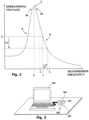
- Fig. 2 is a graph showing how the amplitude of the operational voltage of an inductive power transfer system varies according to the transmission frequency. It is noted that the voltage is at its highest when the transmission frequency is equal to the resonant frequency f R of the system, this maximum amplitude is known as the resonance peak 2. It is further noted that the slope of the graph is steepest in the regions 4a, 4b to either side of the resonance peak 2. Thus in inductive transfer systems, which operate at or around resonance, a small variation in frequency results in a large change in induced voltage. Similarly, a small change in the resonant frequency of the system results in a large change in the induced voltage. For this reason prior art resonant inductive transfer systems are typically very sensitive to small fluctuations in environmental conditions or variations in alignment between the induction coils.
- the driver 230 ( Fig. 1 ) is configured and operable to transmit a driving voltage which oscillates at a transmission frequency which is substantially different from the resonant frequency of the inductive couple.
- the transmission frequency is selected to lie within one of the near-linear regions 6, 8 where the slope of the frequency-amplitude graph is less steep.
- FIG. 3 A schematic diagram is shown representing a laptop computer 340 drawing power from an inductive power outlet 200 via a secondary power receiving unit 300.
- the power receiving unit 300 includes a secondary inductive coil 320 which is aligned to a primary inductive coil 220 in the inductive power outlet 200. Any lateral displacement of the secondary power receiving unit 300 changes the alignment between the secondary inductive coil 320 to the primary inductive coil 220. As a result of the changing alignment, the combined inductance of the coil pair changes which in turn changes the resonant frequency of the system.
- the inductive power outlet 200 transmits power at the resonant frequency of the system, even a small lateral movement would reduce significantly the amplitude of the induced voltage.
- the inductive power outlet 200 transmits power at a frequency in one of the regions 6, 8 to either side of the resonance peak 2 ( Fig. 2 ) where the slope of the resonance graph is much shallower. Consequently, the system has a much larger tolerance of variations such as lateral movement.
- a further feature of embodiments of inductive power outlets transmitting at frequencies above the natural resonant frequency of the system is that if the resonant frequency of the system increases for some reasons, then the transmission voltage increases sharply.
- a peak detector 140 ( Fig. 1 ) is be provided to monitor the transmission voltage of the power outlet 200 and is configured to detect large increases in the transmission voltage indicating an increase in resonant frequency.
- ⁇ R 1 2 ⁇ LC , it is noted that any decrease in either the inductance L or the capacitance C of the system increases the resonant frequency and may be detected by the peak detector 140.
- a peak detector 140 As an example of the use of a peak detector 140, reference is again made to Fig. 3 . It will be appreciated that in a desktop environment, conductive bodies such as a paper clip, metal rule, the metal casing a stapler, a hole-punch or any metallic objects may be introduced between the inductive power outlet 200 and the secondary power receiving unit 300. The oscillating magnetic field produced by the primary coil 220 would then produce eddy currents in the conductive body heating it and thereby draining power from the primary coil 220. Such a power drain may be wasteful and/or dangerous. Power drains such as described above generally reduce the inductance L of the system thereby increasing its resonant frequency.
- the inductance L of the system may also be reduced by the removal of the secondary coil 220, the creation of a short circuit or the like.
- a peak detector 140 wired to the inductive power outlet, may detect any of these scenarios as a large increase in transmission voltage.
- the power transfer system may be further configured to shut down, issue a warning or otherwise protect the user and the system in the event that the peak detector 140 detects such an increase in transmission voltage.
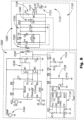
- Fig. 4 is a circuit diagram of an inductive power outlet 6200 and secondary unit 6300.
- the secondary unit 6300 comprises a secondary coil 6320 wired to an electric load 6340 via a rectifier 6330.
- the inductive power outlet 6200 comprises a primary coil 6220 driven by a half-bridge converter 6230 connected to a power source 6240.
- the half-bridge converter 6230 is configured to drive the primary coil 6220 at a frequency higher than the resonant frequency of the system and a peak detector 6140 is configured to detect increases in the transmission voltage.
- a half-bridge converter is represented in Fig. 4 , it is noted that other possible driving circuits include: a DC-to-DC converter, an AC-to-DC converter, an AC-to-AC converter, a flyback transformer, a full-bridge converter, a flyback converter or a forward converter for example.
- the transmission frequency may be used to regulate power transfer.
- Prior art inductive power transfer systems typically regulate power transfer by altering the duty cycle of the transmission voltage.
- the driver 230 may be configured to regulate power transfer by adjusting the transmission frequency.
- the frequency of transmission may be selected to be in the approximately linear region 8 of the curve between a lower frequency value of f L and an upper frequency value of f U .
- a transmission frequency f t higher than the resonant frequency f R of the system, produces an induced voltage of V t .
- the induced voltage can be increased by reducing the transmission frequency so that it is closer to the resonant frequency f R .
- the induced voltage may be reduced by increasing the transmission frequency so that it is further from the resonant frequency f R .
- an adjustment of transmission frequency by ⁇ f produces a change in induced voltage of ⁇ V.
- a communication channel 120 ( Fig. 1 ) is provided between the secondary unit 300 and the inductive power outlet 200 to communicate the required operating parameters.
- operating parameters the communication channel 120 may be used to indicate the transmission frequency required by the electric load 340 to the driver 230.
- the communication channel 120 may further provide a feedback signal during power transmission.
- the feedback transmission may communicate required or monitored operating parameters of the electric load 240 such as:
- a microcontroller in the driver 230 may use such feedback parameters to calculate the required transmission frequency and to adjust the driver accordingly.
- simple feedback signals may be provided indicating whether more or less power is required.
- a power regulation method using simple feedback signals is shown in the flowchart of Fig. 5 .
- the method involves the following steps:
- the operating parameters of the electric load may be monitored and their values may be transmitted to the power outlet via the communications channel 120.
- a processor in the power outlet may then calculate the required transmission frequency directly.
- the method described hereabove refers to a non-resonant transmission frequency lying within the linear region 8 ( Fig. 2 ), higher than the resonant peak 2. It will be appreciated however that in alternative embodiments frequency-controlled power regulation may be achieved when the transmission frequency lies in the lower linear region of the resonance curve. Nevertheless, for certain embodiments, the selection of transmission frequencies in the higher linear 8 may be preferred, particularly where peak detection, as described above, is required.
- various transmitters 122 and receivers 124 may be used for the communication channel 120.
- the primary and secondary coils 220, 320 are galvanically isolated optocouplers, for example, may be used.
- a light emitting diode serves as a transmitter and sends encoded optical signals over short distances to a photo-transistor which serves as a receiver.
- optocouplers typically need to be aligned such that there is a line-of-sight between transmitter and receiver. In systems where alignment between the transmitter and receiver may be difficult to achieve, optocoupling may be inappropriate and alternative systems may be preferred such as ultrasonic signals transmitted by piezoelectric elements or radio signals such as Bluetooth, WiFi and the like.
- the primary and secondary coils 220, 320 may themselves serve as the transmitter 122 and receiver 124.
- an optical transmitter such as a light emitting diode (LED) for example, is incorporated within the secondary unit 300 and is configured and operable to transmit electromagnetic radiation of a type and intensity capable of penetrating the casings of both the secondary unit 300, and the power outlet 200.
- An optical receiver such as a photodiode, a phototransistor, a light dependent resistors of the like, is incorporated within the power outlet 200 for receiving the electromagnetic radiation.
- an inductive communications channel 2120 is incorporated into the inductive power transfer system 2100 for transferring signals between a inductive power outlet 2200 and a remote secondary unit 2300.
- the communication channel 2120 is configured to produce an output signal S out in the power outlet 2200 when an input signal S in is provided by the secondary unit 2300 without interupting the inductive power transfer from the outlet 2200 to the secondary unit 2300.
- the inductive power outlet 2200 includes a primary inductive coil 2220 wired to a power source 2240 via a driver 2230.
- the driver 2230 is configured to provide an oscillating driving voltage to the primary inductive coil 2220, typically at a voltage transmission frequency f t which is higher than the resonant frequency f R of the system.
- the secondary unit 2300 includes a secondary inductive coil 2320, wired to an electric load 2340, which is inductively coupled to the primary inductive coil 2220.
- the electric load 2340 draws power from the power source 2240.
- a rectifier 2330 may be provided to rectify the alternating current signal induced in the secondary coil 2320.
- An inductive communication channel 2120 is provided for transferring signals from the secondary inductive coil 2320 to the primary inductive coil 2220 concurrently with uninterrupted inductive power transfer from the primary inductive coil 2220 to the secondary inductive coil 2320.
- the communication channel 2120 may provide feedback signals to the driver 2230.
- the inductive communication channel 2120 includes a transmission circuit 2122 and a receiving circuit 2124.
- the transmission circuit 2122 is wired to the secondary coil 2320, optionally via a rectifier 2330, and the receiving circuit 2124 is wired to the primary coil 2220.
- the signal transmission circuit 2122 includes at least one electrical element 2126, selected such that when it is connected to the secondary coil 2320, the resonant frequency f R of the system increases.
- the transmission circuit 2122 is configured to selectively connect the electrical element 2126 to the secondary coil 2320.
- any decrease in either the inductance L or the capacitance C increases the resonant frequency of the system.
- the electrical element 2126 may be have a low resistance for example, with a resistance say under 50 ohms and Optionally about 1 ohm.
- the signal receiving circuit 2124 includes a voltage peak detector 2128 configured to detect large increases in the transmission voltage.
- a voltage peak detector 2128 configured to detect large increases in the transmission voltage.
- the transmission circuit 2122 may be used to send a signal pulse to the receiving circuit 2124 and a coded signal may be constructed from such pulses.
- the transmission circuit 2122 may also include a modulator (not shown) for modulating a bit-rate signal with the input signal Sin.
- the electrical element 2126 may then be connected to the secondary inductive coil 2320 according to the modulated signal.
- the receiving circuit 2124 may include a demodulator (not shown) for demodulating the modulated signal.
- the voltage peak detector 2128 may be connected to a correlator for cross-correlating the amplitude of the primary voltage with the bit-rate signal thereby producing the output signal Sout.
- a plurality of electrical elements 2126 may be provided which may be selectively connected to induce a plurality of voltage peaks of varying sizes in the amplitude of the primary voltage.
- the size of the voltage peak detected by the peak detector 2128 may be used to transfer multiple signals.
- Fig. 7 is a graph showing how the amplitude of the operational voltage varies according to the transmission frequency. It is noted that the voltage is at its highest when the transmission frequency is equal to the resonant frequency f R of the system, this maximum amplitude is known as the resonance peak 2. If the resonant frequency f R of the system increases, a new resonance peak 2' is produced.
- an inductive power transfer system 2100 operates at a given transmission frequency f t which is higher than the resonant frequency f R of the system.
- the normal operating voltage V t is monitored by the voltage peak detector 2128.
- the electric element 2126 When the electric element 2126 is connected to the secondary inductive coil 2320 the resonant frequency of the system increases. Therefore, the operating voltage increases to a higher value V t '. This increase is detected by the voltage peak detector 2128.
- the present invention enables data signals to be transferred from the secondary coil 2320 to the primary coil 2220 concurrently with inductive transfer of power from the primary coil 2220 to the secondary coil 2320. Consequently, the signal transfer system may be used to provide feedback signals for real time power regulation.
- Fig. 8 shows an exemplary circuit diagram of an inductive power outlet 7200 and a secondary unit 7300, according to another embodiment of the invention.
- An inductive feedback channel 7120 is provided for transferring signals between the coils concurrently with uninterrupted inductive power transfer.
- the inductive power outlet 7200 comprises a primary coil 7220 driven by a half-bridge converter 7230 connected to a power source 7240.
- the half-bridge converter 7230 is configured to drive the primary coil 7220 at a frequency higher than the resonant frequency of the system.
- the secondary unit 7300 comprises a secondary coil 7320 wired to the input terminals T 1 , T 2 of a rectifier 7330, and an electric load 7340 wired to the output terminals T 3 , T 4 of the rectifier 7330.
- the inductive feedback channel 7120 comprises a transmission circuit 7122, in the secondary unit 7300 and a receiving circuit 7124 in the inductive power outlet 7200.
- the transmission circuit 7122 comprises an electrical resistor 7126 connected to the rectifier 7330 via a power MOSFET switch 7125.
- a modulator 7123 may provide an input signal S in to the power MOSFET 7125.
- the transmission circuit 7122 is wired to one input terminal T 1 and one output terminal T 3 of the rectifier 7330. This configuration is particularly advantageous as, even when the transmission circuit 7122 is connected, the resistor 7126 only draws power from the system during one half of the AC cycle, thereby significantly reducing power loss.
- the receiving circuit 7124 includes a voltage peak detector 7128 that is configured to detect increases in the transmission voltage, and a demodulator 7129 for producing an output signal S out .
- a flowchart is presented showing the main steps in a method for transferring a signal from the secondary inductive coil to a primary inductive coil of an inductive power transfer system.
- the method includes the following steps:
- the inductive communication channel 2120 may be used to transfer a feedback signal from the secondary inductive coil to the primary inductive coil for regulating power transfer across an inductive power coupling as described above.
- Inductive power receivers may be used to wirelessly provide power for a variety of electrical devices.
- Embodiments of the present invention may be integrated into such inductive power receivers.
- heat loss from the non-resonant system is lower.
- embodiments of the current invention may be of particular use when incorporated within high power applications such as power tools, kitchen appliances, bathroom appliances, computers, media players, office equipment and the like.
- the reduced heat loss, associated with embodiments of the non-resonant systems of the invention, is particularly useful when heat dissipation is difficult for example when power receiver has small dimensions or for heat-sensitive equipment such as measuring devices. Also, it is desirable that devices implanted into a living body do not dissipate large amounts of heat into the body. Therefore, non-resonant inductive transfer is well suited to implanted devices, such as pace makers, trackers and the like. It is also noted that in recent years public concern about the threat of a global energy crisis has resulted in a greater emphasis being placed upon optimizing the efficiency of energy transfer. It is difficult to achieve more demanding specifications using existing technology and, in this context, embodiments of the present invention may be used to provide high powers with very low energy losses. Consequently the current invention is an important element in the drive for greater efficiency.
- embodiments of the present invention may be advantageously utilized in inductive power transfer systems in any of the various applications in which power is transferred from a primary coil to a remote secondary coil.
- applications include:
- the inductive transfer system has a higher tolerance to environmental fluctuations and variations in inductive coil alignment than other transfer systems and the frequency may be used to regulate power transfer.
- a peak detector may be used to indicate hazards and provide an inductive communication channel.
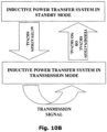
- the inductive power transfer system 1000 includes an inductive power outlet 1200 and an inductive power receiver 1300 and is configured to switch between transmission mode and standby mode.
- the system 1000 may be dormant with the inductive power outlet 1200 and inductive power receiver 1300 waiting for an activation signal before transitioning to transmission mode.
- the inductive power system 1000 is configured and operable to draw power from a power supply 1240, such as a mains electricity supply, a vehicle battery, a power generator, fuel cell or the like, to an electric load 1340.
- an inductive power transfer system 1000 may significantly reduce power losses associated with prior art power transfer systems.
- the inductive power outlet 1200 may be configured to switch to transmission mode only in the presence of a suitable inductive power receiver 1300.
- the system 1000 may be operable to revert to standby mode when no power need be transferred, for example when the inductive power receiver 1300 is removed or the electric load 1340 requires no further power. Thus power is only drawn by the system 1000 when actually required.
- Various activation and termination protocols may be used with the system, such as described hereinbelow.
- the inductive power transfer system 1000 may switch between standby mode and transmission mode by a number of pathways.
- the inductive power outlet 1200 or the inductive power receiver 1300 may be configured to wait for an activation signal. If such an activation signal is received, the system 1000 may switch to transmission mode.
- activation of the system 1000 may involve an initial trigger signal activating the inductive power outlet 1200 and an authentication process confirming the presence of a suitable inductive power receiver 1300.
- the inductive power transfer system 1000 may be configured to periodically transfer signals between the inductive power receiver 1300 and the inductive power outlet 1200, such as described hereinabove in relation to Fig. 5 , for example.
- various transmission signals may be used with the system, for example, instructions may be sent from the inductive power receiver 1300 to the inductive power outlet 1200 to increase power by a certain interval, to decrease power by a certain interval, to maintain the same power, to terminate power transfer or the like. Where no such transmission signals are received, the inductive power outlet 1200 may be configured to stop driving the primary inductor 1220 and to revert to the standby mode.
- the inductive power transfer system 1000 may be configured to revert to standby mode when a termination signal is transferred between the inductive power receiver 1300 and the inductive power outlet 1200.
- the inductive power receiver 1300 may be configured to send a termination signal to the inductive power outlet 1200 when the electric load 1340 no longer requires power.
- a termination signal may be generated when the electrical cell is fully charged.
- an inductive power transfer system such as disclosed herein may reduce significantly the amount of power drawn by dormant power adaptors, chargers and the like.
- the system 1000 may include a trigger mechanism 1400 and a signal transfer mechanism 1120.
- the trigger mechanism 1400 may be used while the inductive power transfer system 1000 is in the standby mode, to provide an initial trigger to generate an activation signal such that the inductive power transfer system 1000 switches to transmission mode.
- the signal transfer mechanism 1120 may provide a channel for the inductive power receiver 1300 to send instruction signals, such as identification signals, authentication signals, transmission signals, termination signals or the like to the inductive power outlet 1200.
- the inductive power outlet 1200 of the inductive power transfer system 1000 includes a primary inductor 1220 such as a primary inductive coil, for example, connectable to the power supply 1240 via a driver 1230.
- the driver 1230 provides the electronics necessary for supplying an oscillating voltage to the inductive coil 1220.
- the inductive power receiver 1300 typically includes a secondary inductor 1320, such as a secondary inductive coil, a regulator 1330 and an electrical load 1340.
- the secondary inductive coil 1320 is configured to inductively couple with the primary inductive coil 1220 of the inductive power outlet 1200.
- the regulator 1330 may include a rectifier to convert alternating current induced across the secondary coil 1320 to a direct current signal for supplying the electrical load 1340.
- a rectifier 1330 may be necessary, for example, where the electrical load 1340 comprises an electrochemical cell to be charged.
- the trigger mechanism 1400 may control the connection between the power supply 1240 and the inductive power outlet 1200.
- the trigger mechanism 1400 may include a circuit breaker 1420 and a trigger sensor1440.
- trigger mechanism 1400 may further include an auxiliary power source 1460 for providing power when the inductive power outlet 1200 is disconnected from its power supply 1240.
- auxiliary power sources 1460 may be used in embodiments of the trigger mechanism 1400 such as electrochemical cells, capacitors and the like, which may be configured to store energy while the inductive power outlet 1200 is connected to the power supply 1240 for use when the inductive power outlet 1200 is disconnected.
- Still other auxiliary power sources may include electricity generating elements such as solar cells, piezoelectric elements, dynamos or the like.
- the circuit breaker 1420 may be configured to receive a disabling signal from the trigger and in response to provide an electrical connection between the power supply 1240 and the inductive power outlet 1200.
- Various circuit breakers 1420 may be used to disconnect the inductive power outlet 1200 from the power supply 1240 as suit requirements.
- an electronic switch may be provided such as a Metal-Oxide Semiconductor Field-Effect Transistor (MOSFET) or the like the gate terminal of which may be configured to receive the electrical signals sent by the trigger sensor 1440.
- MOSFET Metal-Oxide Semiconductor Field-Effect Transistor
- Other circuit breakers may include for example, a single pole switch, a double pole switch, a throw switch or the like.
- the trigger sensor 1440 is configured to detect a release signal indicating the proximity of a possible inductive power receiver 1300.
- the trigger 1440 may be further configured to disable the circuit breaker 1420 when the release signal is detected.
- an activator 1480 incorporated into the inductive power receiver 1300 is configured to produce the release signal which is detectable by the trigger 1440.
- the trigger mechanism 1400 may include a magnetic detector such as a Hall Effect switch, reed switch or the like.
- the magnetic switch may be configured to detect an increase in magnetic field as a result of the approach of an activating magnetic element associated with the inductive power receiver 1300.
- a Hall Effect switch may be configured to detect the approach of an alignment magnet associated with the inductive power receiver 1300 which further functions as the activating magnetic element 1480 for the trigger mechanism 1400.
- other magnetic switches may be used in other embodiments of the trigger mechanism as will occur to the skilled practitioner.
- Still other embodiments of the trigger mechanism may be used, for example, as described in the applicants co-pending patent application PCT/IL2010/001013 which is incorporated herein by reference.
- the signal transfer system 1120 may include an inductive feedback channel 7120 such as described hereinabove in relation to Fig. 8 .
- the regulator 1330 of the inductive power receiver may be in communication with a transmission circuit 1122 including a signal generator 1123, a switching unit 1125 and an ancillary load 1340.
- the signal generator 1123 may be a modulator 7123 such as described in Fig. 8 .
- the switching unit 1125 may be a MOSFET 7125 such as described in Fig. 8 .
- the ancillary load 1126 may be an electrical resistor 7126 such as described in Fig. 8 , although other electrical elements such as capacitors, inductors and the like may alternatively or additionally serve as the ancillary load 1126.
- the transmission circuit 1122 may thus modulate the power drawn by the secondary inductor 1320.
- the modulated power may be detected by a signal detector 1124 associated with the inductive power outlet 1200.
- the inductive power outlet 1200 includes a signal detector 1124 comprising a peak detector 1128 and a processor 1129.
- the peak detector 1128 may be configured to detect peaks in primary voltage across the primary inductor or primary current supplied to the primary inductor. Thus, the peak detector 1128 may be able to detect when the ancillary load is connected to the secondary inductor 1320.
- the processor 1129 such as the demodulator 7129 described above in relation to Fig. 8 , may be provided to determine the frequency of peak pulses.
- the signal transfer system 1120 may be used to transmit instruction signals such as identification signals, authentication signals, transmission signals, termination signals or the like to the inductive power outlet 1200 in the form of peak pulses having characteristic frequencies.
- the regulator 1330 of the inductive power receiver 1300 which may include a controller, rectifier, capacitors, microcontroller, voltage monitor or the like, is in communication with the transmission circuit 1122.
- the regulator 1330 may be operable to monitor induced secondary voltage across the secondary inductor 1320 and to compare the induced voltage with reference values. By comparing the secondary voltage with threshold values, the regulator 1330 may determine whether the secondary voltage lies within a permissible range of values.
- instruction signals may be selected by the regulator 1330 and generated by the transmission circuit 1122 instructing the inductive power outlet 1200 to adjust the induced voltage across the secondary inductor 1320.
- the regulator 1320 and transmission circuit 1122 may be further operable to respond to an activation voltage pulse induced across secondary inductor 1320 by generating an identification instruction signal (ID signal).
- ID signal may be detected by the inductive power outlet 1200 thereby confirming the presence of the inductive power receiver 1300 and optionally its required operating parameters.
- Fig. 11A showing selected stages of a possible protocol for transition from standby phase to the transmission phase in the inductive power outlet.
- the dormant inductive power outlet waits for a release signal 1002.
- the release signal indicates to the inductive power outlet that a compatible inductive power receiver may have been placed within transmission range.
- a release signal may be inter alia a change in local magnetic field associated with a trigger magnet in the inductive power receiver.
- the inductive power outlet incorporates a Hall switch which is configured to detect changes in the local magnetic field.
- Other release signal mechanisms will occur to those skilled in the art such as signals detectable using piezoelectric elements, light sensors, audio sensors and the like as suit requirements.
- the outlet remains in standby mode 1004.
- an authentication process 1005 is initiated during which the presence of the inductive power receiver is confirmed.
- the authentication process may start by the driver of the primary inductor producing an initial power of sufficient intensity to induce an activation voltage pulse across the secondary inductor of the inductive power receiver 1006.
- a primary voltage may be driven across the primary inductor such that an activation voltage pulse of eight volts is induced across the secondary inductor.
- the inductive power outlet may be operable to detect an ID signal in response to the initial power burst 1008. If the inductive power outlet receives an ID signal response from a recognized inductive power receiver, then the ID signal may be identified 1010 and the mode switched to transmission mode 1016. Optionally, depending upon the identity of the ID signal, an initial transmission power level may be selected 1012 according to what ID signal is received and the primary inductor driven with the initial transmission power level 1014. Alternatively, the initial transmission power level may be the transmission power level of the initial power burst.
- the initial power burst across the primary inductor may be repeated for a fixed number of iterations before the inductive power outlet reverts to standby mode.
- the driving voltage of the initial power burst may be constant or changing.
- the driver of the inductive power outlet may be operable to produce an initial 15 millisecond burst of oscillating voltage across which may repeated, say every 256 milliseconds or so. After five iterations or so, if no ID signal is received, the inductive power outlet may revert to standby mode.
- ID signals may be used in embodiments of the present disclosure, for example, where the inductive power outlet includes a peak detector, as described hereinabove, a transmission circuit may be used to modulate the primary voltage across the primary inductor, or primary current drawn by the primary inductor, with peak pulses having characteristic frequencies which are identifiable as generated by recognized inductive power receivers.
- ID signals may peak pulses having characteristic frequencies selected from 500 hertz, 1 kilohertz and 8 kilohertz. The selected characteristic frequency of the ID signal may provide further instructions to the inductive power outlet for example relating to required transmission parameters, user specific data, billing information or the like.
- the power level of the induced voltage may be regulated by adjusting a variety of parameters of the driving voltage. For example, where non-resonant power transmission is used, such as described hereinabove, the power level may be determined by the selected operating frequency. Optionally, the initial voltage across the primary inductor may be steadily increased by decreasing the driving frequency from 476 kilohertz to 313 kilohertz during the initial burst. Alternatively, a the power level may be selected by adjusting the duty cycle or amplitude of the driving voltage.
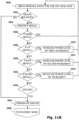
- Fig. 11B representing a possible transmission mode protocol for use with an inductive power outlet. Optionally, such a protocol may be initiated by the transition protocol of Fig. 11A , alternatively an inductive power outlet may be activated in other ways, such as by manually operating a power switch, connecting to a mains power supply or the like.
- the inductive power outlet may be operable to drive the primary inductor for a limited time duration 1020, for example for 10 milliseconds or so. At the end of the limited time duration, the outlet may be operable to terminate the operation 1036 unless an instruction signal is received 1022.
- Such a system may enable an energy efficient inductive power outlet to draw power only when required and to shut down when not needed. If an instruction signal is received from the inductive power receiver, the signal may be identified 1024 and acted upon, for example, as follows:
- the transmission protocol and for illustrative purposes only, an example of the protocol is described below in in which the inductive power outlet drives a non-resonant transmission voltage.
- the protocol may also be applicable to resonant transmission systems.
- the instruction signals may comprise modulated peak pulses with each signal having a characteristic frequency.
- the perpetuation signal P-SAME may have a characteristic frequency of 500 hertz
- the first power increase signal P-UP may have a characteristic frequency of 8 kilohertz
- the second power increase signal P-DUP may have a characteristic frequency of between 1.5 and 5 kilohertz
- the termination signal END-SIG may have a characteristic frequency of 250 hertz. It will be appreciated that other characteristic frequencies may alternatively be used. Indeed, where required, other instruction signals, such as additional power decrease signal, for example, may be additionally or alternatively transferred as suit requirements.
- the output power of the secondary inductor may be regulated by increasing or decreasing the driving frequency by incremental amounts.
- the incremental frequency steps ⁇ f may be selected from within a permissible range of 277 kilohertz to 357 kilohertz or so.
- two power increase signals P-UP and P-DUP may request different incremental power increases. Accordingly the second power increase signal P-DUP may be used to step up power by larger increments, say twice the size of the standard increments. This may be useful for example where the initial voltage is particularly low.
- the inductive power receiver may be activated when a voltage is induced across the secondary inductor 1040, when the regulator may detect the activation voltage 1042 an identification signal may be sent to the inductive power outlet 1044.
- Such an identification signal may serve to switch the inductive power transmitter to transmission mode as described above in relation to Fig. 11A .
- an induced voltage of about 8V and producing a current of about 3 milliamps and lasting about 5 milliseconds or so may power a microcontroller associated with the regulator to activate the sending of an ID signal to the inductive power outlet.
- a transmission circuit 1122 ( Fig. 10 ) may be used to produce a modulated peak pulse having a characteristic frequency selected from 500 hertz, 1 kilohertz, 8 kilohertz or the like.
- the inductive power receiver may select an ID signal such that predetermined transmission parameters may be selected for operating the inductive power outlet.
- the inductive power receiver is operable to periodically send instruction signals to the inductive power outlet.
- the instruction signals may be selected according to various factors as outlined below.
- the inductive power receiver is operable to detect an end-of-charge command EOC-SIG indicating that the electric load, such as an electrochemical cell or the like, requires no more power 1046. If such an end-of-charge command is detected, the inductive power receiver may be operable to send a termination signal END-SIG to the inductive power transmitter 1064. As outlined above in relation to Fig. 11B , the termination signal instruct the inductive power outlet to revert to standby mode.
- the termination signal comprises a modulated peak pulse having a characteristic frequency of 250 hertz. It will be appreciated that such a termination mechanism may enable an energy efficient inductive power transfer system to draw power only when required and to shut down when not needed thereby reducing energy wastage.
- the regulator may be configured to compare the output of the secondary inductor to at least one reference value 1048.
- the regulator may compare secondary voltage to reference values stored in a memory element.
- reference values may be calculated by a processor associated with the inductive power receiver to suit requirements.
- a first power increase signal P-UP may be sent to the inductive power outlet 1058.
- the regulator may further compare the power to a second threshold value Th 2 1052, if the power is also lower than the second threshold value Th 2 a second power increase signal P-DUP may be sent to the inductive power outlet 1056.
- the power may be compared to at least one an upper threshold value Th 3 1054. If the power level is greater than the upper threshold value Th 3 , then a power decrease signal P-DOWN may be sent to the inductive power outlet 1060.
- a perpetuation signal P-SAME may be sent to the inductive power outlet 1062.
- a signal is sent at least one instruction signal may be sent to the inductive power outlet during each time duration.
- the inductive power receiver may periodically indicate its continued presence to the inductive power outlet. It will be appreciated that when the inductive power receiver is removed from the inducitive power outlet, no instruction signals will be passed therebetween. As indicated above in relation to Fig. 11B , the inductive power outlet may be configured to shut down when no such signal is received.
- instruction signals Although only five instruction signals are described hereinabove, other instruction signals may be additionally be transferred as required. Various instructions may occur to those skilled in the art, for example indicating that the power is outside still further threshold values, requesting greater power resolution or such like.
Landscapes
- Engineering & Computer Science (AREA)
- Power Engineering (AREA)
- Computer Networks & Wireless Communication (AREA)
- Signal Processing (AREA)
- Near-Field Transmission Systems (AREA)
- Charge And Discharge Circuits For Batteries Or The Like (AREA)
- Testing Of Short-Circuits, Discontinuities, Leakage, Or Incorrect Line Connections (AREA)
Claims (2)
- Induktiver Stromausgang (1200) zum Übertragen von Strom an mindestens einen induktiven Stromempfänger (1300), wobei der induktive Stromausgang umfasst:mindestens eine induktive Primärspule (1220), die mit einer Stromversorgung (1240) verdrahtet ist, wobei die mindestens eine induktive Primärspule (1220) eine induktive Kopplung mit mindestens einer induktiven Sekundärspule (1320) bildet, die dem mindestens einen induktiven Stromempfänger (1300) zugehörig ist;mindestens einen Treiber (1230), der dazu konfiguriert ist, eine oszillierende Spannung an der mindestens einen induktiven Primärspule (1220) bereitzustellen; undmindestens einen Spitzendetektor (1128), der dazu konfiguriert ist, Spitzen in Primärspannung oder Primärstrom zu ermitteln, die erzeugt werden, wenn ein elektrisches Element (1126) mit der mindestens einen induktiven Sekundärspule (1320) verbunden ist, die mit der mindestens einen induktiven Primärspule (1220) gekoppelt ist;wobei der induktive Stromausgang (1200) durch Folgendes gekennzeichnet ist:der induktive Stromausgang (1200) ist so betreibbar, dass er einen Aktivierungsspannungsimpuls an der induktiven Sekundärspule (1320) des induktiven Stromempfängers (1300) induziert, wodurch der induktive Stromempfänger (1300) dazu veranlasst wird, ein Identifikationssignal an den induktiven Stromausgang (1200) zu senden;der mindestens eine Spitzendetektor (1128) dazu betreibbar ist, eine Vielzahl von Befehlssignalen zu erfassen, von denen jedes eine unterschiedliche charakteristische Frequenz der Spitzen der Primärspannung oder des Primärstroms aufweist, und wobei der induktive Stromausgang (1200) des Weiteren mindestens einen Prozessor (1129) aufweist, der dazu betreibbar ist, die unterschiedliche charakteristische Frequenz der Spitzen zu bestimmen,
undwobei die Befehlssignale Folgende sind:ein Impuls von etwa einem Kilohertz, um den induktiven Stromausgang (1200) dazu anzuweisen, die Betriebsleistung um eine erste Stufe zu erhöhen;ein Impuls von etwa 8 Kilohertz, um den induktiven Stromausgang (1200) dazu anzuweisen, die Betriebsleistung um eine erste Stufe zu erhöhen;ein Impuls von etwa 500 Hertz, um den induktiven Stromausgang (1200) dazu anzuweisen, die Ansteuerung der induktiven Primärspule (1220) mit derselben Leistung fortzusetzen; undein Impuls von etwa 250 Hertz, um den induktiven Stromausgang (1200) dazu anzuweisen, die Ansteuerung der induktiven Primärspule (1220) zu beenden. - Induktiver Stromausgang nach Anspruch 1, des Weiteren umfassend einen Auslösesensor (1440), der dazu konfiguriert ist, ein Auslösesignal zu ermitteln, welches die Nähe eines möglichen induktiven Stromempfängers (1200) anzeigt.
Priority Applications (2)
| Application Number | Priority Date | Filing Date | Title |
|---|---|---|---|
| EP23174902.9A EP4250530A3 (de) | 2011-08-09 | 2011-09-05 | Induktive energiequelle und entsprechender empfänger |
| EP20202918.7A EP3787152B1 (de) | 2011-08-09 | 2011-09-05 | Induktive energiequelle und entsprechender empfänger |
Applications Claiming Priority (2)
| Application Number | Priority Date | Filing Date | Title |
|---|---|---|---|
| US13/205,672 US8981598B2 (en) | 2008-07-02 | 2011-08-09 | Energy efficient inductive power transmission system and method |
| PCT/IL2011/000706 WO2013021371A1 (en) | 2011-08-09 | 2011-09-05 | Energy efficient inductive power transmission system and method |
Related Child Applications (4)
| Application Number | Title | Priority Date | Filing Date |
|---|---|---|---|
| EP20202918.7A Division EP3787152B1 (de) | 2011-08-09 | 2011-09-05 | Induktive energiequelle und entsprechender empfänger |
| EP20202918.7A Division-Into EP3787152B1 (de) | 2011-08-09 | 2011-09-05 | Induktive energiequelle und entsprechender empfänger |
| EP23174902.9A Division EP4250530A3 (de) | 2011-08-09 | 2011-09-05 | Induktive energiequelle und entsprechender empfänger |
| EP23174902.9A Division-Into EP4250530A3 (de) | 2011-08-09 | 2011-09-05 | Induktive energiequelle und entsprechender empfänger |
Publications (3)
| Publication Number | Publication Date |
|---|---|
| EP2774244A1 EP2774244A1 (de) | 2014-09-10 |
| EP2774244B1 EP2774244B1 (de) | 2020-11-04 |
| EP2774244B2 true EP2774244B2 (de) | 2024-04-10 |
Family
ID=45003014
Family Applications (3)
| Application Number | Title | Priority Date | Filing Date |
|---|---|---|---|
| EP11773322.0A Active EP2774244B2 (de) | 2011-08-09 | 2011-09-05 | Energieeffiziente induktives stromübertragungssystem und verfahren dafür |
| EP23174902.9A Pending EP4250530A3 (de) | 2011-08-09 | 2011-09-05 | Induktive energiequelle und entsprechender empfänger |
| EP20202918.7A Active EP3787152B1 (de) | 2011-08-09 | 2011-09-05 | Induktive energiequelle und entsprechender empfänger |
Family Applications After (2)
| Application Number | Title | Priority Date | Filing Date |
|---|---|---|---|
| EP23174902.9A Pending EP4250530A3 (de) | 2011-08-09 | 2011-09-05 | Induktive energiequelle und entsprechender empfänger |
| EP20202918.7A Active EP3787152B1 (de) | 2011-08-09 | 2011-09-05 | Induktive energiequelle und entsprechender empfänger |
Country Status (5)
| Country | Link |
|---|---|
| US (6) | US8981598B2 (de) |
| EP (3) | EP2774244B2 (de) |
| KR (1) | KR20140053297A (de) |
| CN (1) | CN103975497A (de) |
| WO (1) | WO2013021371A1 (de) |
Families Citing this family (59)
| Publication number | Priority date | Publication date | Assignee | Title |
|---|---|---|---|---|
| ES2687775T3 (es) | 2008-12-12 | 2018-10-29 | Ge Hybrid Technologies, Llc | Estación de carga sin contacto equipada con un núcleo de PTPS que tiene una estructura de núcleo en espiral plana, un aparato de recepción de energía sin contacto y un procedimiento para controlar la misma |
| US11476566B2 (en) * | 2009-03-09 | 2022-10-18 | Nucurrent, Inc. | Multi-layer-multi-turn structure for high efficiency wireless communication |
| US10056944B2 (en) | 2011-02-01 | 2018-08-21 | Fu Da Tong Technology Co., Ltd. | Data determination method for supplying-end module of induction type power supply system and related supplying-end module |
| TWI570427B (zh) | 2015-10-28 | 2017-02-11 | 富達通科技股份有限公司 | 感應式電源供應器及其金屬異物檢測方法 |
| US10630113B2 (en) | 2011-02-01 | 2020-04-21 | Fu Da Tong Technology Co., Ltd | Power supply device of induction type power supply system and RF magnetic card identification method of the same |
| US9600021B2 (en) | 2011-02-01 | 2017-03-21 | Fu Da Tong Technology Co., Ltd. | Operating clock synchronization adjusting method for induction type power supply system |
| TWI568125B (zh) * | 2015-01-14 | 2017-01-21 | 富達通科技股份有限公司 | 感應式電源供應器之供電模組及其電壓測量方法 |
| US10289142B2 (en) | 2011-02-01 | 2019-05-14 | Fu Da Tong Technology Co., Ltd. | Induction type power supply system and intruding metal detection method thereof |
| US9671444B2 (en) | 2011-02-01 | 2017-06-06 | Fu Da Tong Technology Co., Ltd. | Current signal sensing method for supplying-end module of induction type power supply system |
| US9628147B2 (en) | 2011-02-01 | 2017-04-18 | Fu Da Tong Technology Co., Ltd. | Method of automatically adjusting determination voltage and voltage adjusting device thereof |
| US10038338B2 (en) | 2011-02-01 | 2018-07-31 | Fu Da Tong Technology Co., Ltd. | Signal modulation method and signal rectification and modulation device |
| US10615645B2 (en) | 2011-02-01 | 2020-04-07 | Fu Da Tong Technology Co., Ltd | Power supply device of induction type power supply system and NFC device identification method of the same |
| US10312748B2 (en) | 2011-02-01 | 2019-06-04 | Fu Da Tong Techology Co., Ltd. | Signal analysis method and circuit |
| US9831687B2 (en) | 2011-02-01 | 2017-11-28 | Fu Da Tong Technology Co., Ltd. | Supplying-end module for induction-type power supply system and signal analysis circuit therein |
| US9508487B2 (en) | 2011-10-21 | 2016-11-29 | Qualcomm Incorporated | Systems and methods for limiting voltage in wireless power receivers |
| KR101732193B1 (ko) * | 2011-10-21 | 2017-05-04 | 삼성전자주식회사 | 충전 전력 제어 방법 및 이를 위한 무선 충전 장치 |
| CN107276100A (zh) * | 2011-12-28 | 2017-10-20 | 卢特龙电子公司 | 负载控制系统、广播控制器、rf接收装置和无线控制器 |
| US10770927B2 (en) | 2012-07-05 | 2020-09-08 | Powermat Technologies Ltd. | System and method for providing inductive power at multiple power levels |
| KR102074475B1 (ko) | 2012-07-10 | 2020-02-06 | 지이 하이브리드 테크놀로지스, 엘엘씨 | 무선 전력 전송 시스템에서 이물질 감지 장치 및 방법 |
| US9859755B2 (en) | 2012-07-16 | 2018-01-02 | Qualcomm Incorporated | Device alignment and identification in inductive power transfer systems |
| KR101615669B1 (ko) * | 2012-10-11 | 2016-05-11 | 파워매트 테크놀로지스 엘티디. | 디지털 메시지들을 동시에 송신하기 위한 유도 전력 송신 시스템 및 방법 |
| US9564776B2 (en) * | 2012-11-07 | 2017-02-07 | Nokia Technologies Oy | Determining presence of a magnet for controlling wireless charging |
| KR102123829B1 (ko) | 2013-01-22 | 2020-06-18 | 삼성전자주식회사 | 무선 전력 전송 장치 및 무선 전력 전송 방법 |
| US20140253026A1 (en) * | 2013-03-08 | 2014-09-11 | O2 Micro Inc. | Apparatus, Method, and System for Wirelessly Charging an Electronic Device |
| CN107659300B (zh) * | 2013-06-17 | 2021-08-27 | 英飞凌科技股份有限公司 | 用于双向数据传输的电路装置及方法 |
| JP6276532B2 (ja) * | 2013-07-29 | 2018-02-07 | キヤノン株式会社 | 受電装置、送電装置およびそれらの制御方法並びにプログラム |
| US9793739B2 (en) | 2013-08-07 | 2017-10-17 | Sandisk Technologies Llc | Wireless power transmitting device |
| WO2015044943A1 (en) * | 2013-09-24 | 2015-04-02 | Powermat Technologies Ltd. | System and method for increasing operational range of inductive power transmission |
| US9680321B2 (en) * | 2013-11-13 | 2017-06-13 | Kabushiki Kaisha Toshiba | Feeding apparatus and feeding method |
| US10116230B2 (en) | 2013-12-30 | 2018-10-30 | Eaton Capital Unlimited Company | Methods, circuits and articles of manufacture for configuring DC output filter circuits |
| US20170194815A1 (en) * | 2014-05-08 | 2017-07-06 | Powermat Technologies Ltd. | Unified inductive digital protocol |
| US9991753B2 (en) * | 2014-06-11 | 2018-06-05 | Enovate Medical Llc | Variable wireless transfer |
| US9590525B2 (en) * | 2014-07-03 | 2017-03-07 | Eaton Capital | Wireless power transfer systems using load feedback |
| US9630516B2 (en) * | 2014-08-20 | 2017-04-25 | Honda Motor Co., Ltd. | Wireless charging |
| JP6118304B2 (ja) * | 2014-11-14 | 2017-04-19 | 株式会社オートネットワーク技術研究所 | 通信システム及び通信装置 |
| US9984815B2 (en) | 2014-12-22 | 2018-05-29 | Eaton Capital Unlimited Company | Wireless power transfer apparatus and power supplies including overlapping magnetic cores |
| US10038324B2 (en) | 2015-01-06 | 2018-07-31 | Eaton Intelligent Power Limited | Methods, circuits and articles of manufacture for controlling wireless power transfer responsive to controller circuit states |
| US10153665B2 (en) | 2015-01-14 | 2018-12-11 | Fu Da Tong Technology Co., Ltd. | Method for adjusting output power for induction type power supply system and related supplying-end module |
| US10079508B2 (en) * | 2015-01-22 | 2018-09-18 | Integrated Device Technology, Inc. | Apparatuses and related methods for detecting magnetic flux field characteristics with a wireless power receiver |
| US20180090997A1 (en) * | 2015-04-06 | 2018-03-29 | Panasonic Intellectual Property Management Co., Ltd. | Noncontact power supply device and control device therefor |
| US10116144B2 (en) | 2015-05-22 | 2018-10-30 | Eaton Intelligent Power Limited | Wireless power transfer apparatus using enclosures with enhanced magnetic features and methods of fabricating the same |
| WO2016192007A1 (zh) | 2015-06-01 | 2016-12-08 | 广东欧珀移动通信有限公司 | 充电电路和移动终端 |
| US9742128B2 (en) | 2015-06-29 | 2017-08-22 | Grid Connect, Inc. | Smart plug having plug blade detection |
| EP3125065B1 (de) * | 2015-07-31 | 2018-12-19 | Power Integrations Switzerland GmbH | Kommunikation über galvanische isolierung hinweg |
| JP6555010B2 (ja) * | 2015-08-25 | 2019-08-07 | 船井電機株式会社 | 給電装置 |
| EP3136613B1 (de) * | 2015-08-31 | 2021-09-22 | Nokia Technologies Oy | Übertragung eines induktivladungssignals |
| CN108012575B (zh) * | 2015-09-03 | 2021-11-23 | 皇家飞利浦有限公司 | 用于数据和功率的无线传输的设备 |
| US10164600B2 (en) * | 2015-10-12 | 2018-12-25 | Nxp B.V. | NFC or RFID device RF detuning detection and driver output power regulation |
| US10218212B2 (en) | 2016-04-15 | 2019-02-26 | The Gillette Company Llc | System and apparatus for inductive charging of a handheld device |
| US11277030B2 (en) | 2017-03-07 | 2022-03-15 | Powermat Technologies Ltd. | System for wireless power charging |
| KR20230151984A (ko) | 2017-03-07 | 2023-11-02 | 파워매트 테크놀로지스 엘티디. | 무선 전력 충전 시스템 |
| EP3373414B1 (de) | 2017-03-07 | 2019-10-23 | Powermat Technologies Ltd. | System für drahtloses stromladen |
| KR102561310B1 (ko) * | 2017-03-07 | 2023-07-27 | 파워매트 테크놀로지스 엘티디. | 무선 전력 충전 시스템 |
| US10530177B2 (en) * | 2017-03-09 | 2020-01-07 | Cochlear Limited | Multi-loop implant charger |
| WO2018226977A1 (en) | 2017-06-08 | 2018-12-13 | Fossil Group, Inc. | Systems, devices and methods for electrical and/or electronic interconnection |
| EP3496348B1 (de) | 2017-12-05 | 2020-10-14 | Power Integrations Switzerland GmbH | Kommunikation mittels einer induktiven kopplung |
| US11635472B2 (en) * | 2018-05-16 | 2023-04-25 | Hitachi Astemo, Ltd. | Load driving device |
| US11522382B1 (en) | 2018-08-03 | 2022-12-06 | William Vahle | Wireless mobile battery |
| US11990766B2 (en) | 2019-07-02 | 2024-05-21 | Eaton Intelligent Power Limited | Wireless power transfer apparatus with radially arrayed magnetic structures |
Citations (2)
| Publication number | Priority date | Publication date | Assignee | Title |
|---|---|---|---|---|
| US20030151930A1 (en) † | 2001-11-30 | 2003-08-14 | Friwo Geraetebau Gmbh | Inductive contactless power transmitter |
| US20100001845A1 (en) † | 2008-07-03 | 2010-01-07 | Takahiro Yamashita | Method of data transmission embedded in electric power transmission, and a charging stand and battery device using that data transmission |
Family Cites Families (311)
| Publication number | Priority date | Publication date | Assignee | Title |
|---|---|---|---|---|
| US723836A (en) | 1902-10-24 | 1903-03-31 | Percy Foote Cowing | Induction apparatus. |
| US2415688A (en) | 1943-05-05 | 1947-02-11 | Mrs Helen J Hall Jr | Induction device |
| GB778072A (en) | 1954-04-09 | 1957-07-03 | Frank Walter Holland | Improvements in electrical table lamps |
| US3207975A (en) | 1960-05-31 | 1965-09-21 | Intron Int Inc | Circuit employing electronic or semiconductor switch regulating an output voltage |
| FR1462329A (fr) | 1965-10-15 | 1966-04-15 | Materiel Telephonique | Dispositif de commande électrique |
| US3771085A (en) | 1971-08-10 | 1973-11-06 | Tokyo Keiki Kk | Deviation detecting apparatus |
| FR2176499B1 (de) | 1972-03-21 | 1975-03-21 | Salmet Gaston | |
| US3894249A (en) | 1972-12-20 | 1975-07-08 | Matsushita Electric Ind Co Ltd | Device for generating variable output voltage |
| US3995174A (en) | 1974-02-26 | 1976-11-30 | The University Of Toledo | Chopper and chopper-multiplexer circuitry for measurement of remote low-level signals |
| US3938018A (en) | 1974-09-16 | 1976-02-10 | Dahl Ernest A | Induction charging system |
| DE2634303A1 (de) | 1976-07-30 | 1978-02-02 | Knorr Bremse Gmbh | Elektronische schliesseinrichtung |
| US4139880A (en) | 1977-10-03 | 1979-02-13 | Motorola, Inc. | CMOS polarity reversal circuit |
| US4160193A (en) | 1977-11-17 | 1979-07-03 | Richmond Abraham W | Metal vapor electric discharge lamp system |
| DE2752783C2 (de) | 1977-11-25 | 1979-08-30 | Siemens Ag, 1000 Berlin Und 8000 Muenchen | Gerät zum Erfassen und Verarbeiten von elektrischen Signalen |
| US4349814A (en) | 1979-10-08 | 1982-09-14 | Duraplug Electricals Limited | Electric switches |
| US4331496A (en) | 1980-03-10 | 1982-05-25 | The B. F. Goodrich Company | Bearing assembly and method for making same |
| US4319144A (en) | 1980-05-22 | 1982-03-09 | Bell Telephone Laboratories, Incorporated | Single polarity circuit |
| US4423456A (en) | 1981-11-13 | 1983-12-27 | Medtronic, Inc. | Battery reversal protection |
| US4473757A (en) | 1981-12-08 | 1984-09-25 | Intersil, Inc. | Circuit means for converting a bipolar input to a unipolar output |
| US4431948A (en) | 1982-08-09 | 1984-02-14 | Standun Controls, Inc. | Apparatus for control of load power consumption |
| GB2131635B (en) | 1982-12-08 | 1986-08-20 | Siliconix Ltd | Bridge rectifier circuit |
| EP0115747A1 (de) | 1983-01-11 | 1984-08-15 | SAET S.p.A. | Elektronische Diebstahlsicherung mit einem elektronischen Schlüssel |
| US4580062A (en) | 1983-04-21 | 1986-04-01 | Cosden Technology, Inc. | Safety shield control device |
| DE3417455C2 (de) | 1984-05-11 | 1986-07-03 | Licentia Patent-Verwaltungs-Gmbh, 6000 Frankfurt | Einrichtung zur induktiven Energie- und Datenübertragung |
| US4754180A (en) | 1985-04-01 | 1988-06-28 | Honeywell Inc. | Forceless non-contacting power transformer |
| US4970656A (en) | 1986-11-07 | 1990-11-13 | Alcon Laboratories, Inc. | Analog drive for ultrasonic probe with tunable phase angle |
| JPH0739078Y2 (ja) | 1986-11-27 | 1995-09-06 | 株式会社三協精機製作所 | 反転磁気ヘッド装置のテープガイド機構 |
| JPH0747957Y2 (ja) | 1987-03-31 | 1995-11-01 | トツパン・ム−ア株式会社 | 非接触式電力供給装置 |
| US4831508A (en) | 1987-10-20 | 1989-05-16 | Computer Products Inc. | Power supply system having improved input power factor |
| US4977515A (en) | 1988-08-29 | 1990-12-11 | Rudden Frank G | Load management device and method of use |
| DE3881520D1 (de) | 1988-09-05 | 1993-07-08 | Cockerill Sambre Sa | Verfahren zur elektroplattierung zon zinn. |
| JP2697935B2 (ja) | 1989-12-08 | 1998-01-19 | 正雄 中川 | スペクトラム拡散通信を用いたデータ伝送方式 |
| JPH0736556Y2 (ja) | 1990-03-06 | 1995-08-23 | 株式会社ヤマガタグラビヤ | 腰掛け式便器 |
| JPH04156242A (ja) | 1990-10-17 | 1992-05-28 | Sekisui Chem Co Ltd | ワイヤレス給電システム |
| US5119285A (en) | 1991-04-03 | 1992-06-02 | Wayne State University | Solid-state power transformer circuit |
| US5278771A (en) | 1991-07-12 | 1994-01-11 | Seti Corporation | Programmable timed electrical power management device |
| NL9101590A (nl) | 1991-09-20 | 1993-04-16 | Ericsson Radio Systems Bv | Stelsel voor het laden van een oplaadbare accu van een draagbare eenheid in een rek. |
| GB2262634B (en) | 1991-12-18 | 1995-07-12 | Apple Computer | Power connection scheme |
| GB9204200D0 (en) | 1992-02-27 | 1992-04-08 | Goble Nigel M | An inductive loop power transmission system |
| US5221877A (en) | 1992-03-10 | 1993-06-22 | Davis Controls Corporation | Power reduction control for inductive lighting installation |
| JPH0621018A (ja) | 1992-06-29 | 1994-01-28 | Sony Corp | ドライエッチング方法 |
| FR2695285B3 (fr) | 1992-09-02 | 1994-07-29 | Cableco Sa | Ensemble d'eclairage comprenant une lampe alimentee par le secteur. |
| DE4236286A1 (de) | 1992-10-28 | 1994-05-05 | Daimler Benz Ag | Verfahren und Anordnung zum automatischen berührungslosen Laden |
| US5287112A (en) | 1993-04-14 | 1994-02-15 | Texas Instruments Incorporated | High speed read/write AVI system |
| JP3409145B2 (ja) | 1993-07-26 | 2003-05-26 | 任天堂株式会社 | 小型電気機器 |
| JPH0739078A (ja) | 1993-07-26 | 1995-02-07 | Toshiba Corp | 無線電話機の充電装置 |
| US5455466A (en) | 1993-07-29 | 1995-10-03 | Dell Usa, L.P. | Inductive coupling system for power and data transfer |
| EP0727105B1 (de) | 1993-10-21 | 2003-03-12 | Auckland Uniservices Limited | Induktive leitungswicklungen |
| US5530435A (en) | 1993-12-09 | 1996-06-25 | Steelcase Inc. | Utility distribution system for modular furniture and the like |
| JPH0736556U (ja) | 1993-12-13 | 1995-07-04 | 株式会社ユー・アール・ディー | 無結線電力授受装置 |
| JP2671809B2 (ja) | 1994-06-30 | 1997-11-05 | 日本電気株式会社 | 非接触型充電装置 |
| US5762250A (en) | 1994-07-06 | 1998-06-09 | Truckin' Movers Corporation | Convertible carrying case and work platform for small electronic devices |
| JPH10506208A (ja) | 1994-07-19 | 1998-06-16 | エロネックス・テクノロジーズ・インコーポレーテッド | マイクロパーソナルデジタルアシスタント |
| US5486394A (en) | 1994-08-26 | 1996-01-23 | E-Z Taping System, Inc. | Self-release self-adhesive drywall tape |
| IL112928A0 (en) | 1995-03-07 | 1995-06-29 | Neerman Haim | Electronic filter |
| EP0872032B1 (de) | 1995-05-18 | 2003-11-26 | Aura Communications, Inc. | Magnetische kommunikationssystem mit geringer reichweite |
| JPH09103037A (ja) | 1995-10-05 | 1997-04-15 | Nippon Ido Tsushin Kk | 給電装置、被給電装置および給電システム |
| FR2739929B1 (fr) | 1995-10-11 | 1998-01-02 | Marwal Systems | Reservoir de carburant pour vehicule automobile, avec moyens de couplage magnetique pour transmission de signaux |
| DE19546171C1 (de) | 1995-12-11 | 1996-11-28 | Siemens Ag | Diebstahlschutzsystem für ein Kraftfahrzeug |
| FI960358A (fi) | 1996-01-26 | 1997-07-27 | Veijo Sakari Makkonen | Kuulokeväline ja menetelmä kuulokevälineen asettamiseksi |
| EP1061631A1 (de) | 1996-01-30 | 2000-12-20 | Sumitomo Wiring Systems, Ltd. | Verbindungssystem und -verfahren für ein elektrisch betriebenes Fahrzeug |
| EP0791706B1 (de) | 1996-01-31 | 2004-07-14 | Texas Instruments Deutschland Gmbh | Verbesserung für Vollweggleichrichter |
| JPH1023677A (ja) | 1996-07-03 | 1998-01-23 | Uniden Corp | 無接点充電装置、充電器、コードレス機器および無接点充電器 |
| US5821728A (en) | 1996-07-22 | 1998-10-13 | Schwind; John P. | Armature induction charging of moving electric vehicle batteries |
| US5713939A (en) | 1996-09-16 | 1998-02-03 | Sulzer Intermedics Inc. | Data communication system for control of transcutaneous energy transmission to an implantable medical device |
| US5949214A (en) | 1997-11-04 | 1999-09-07 | Input/Output, Inc. | Rechargeable battery pack |
| FR2756679B1 (fr) | 1996-11-29 | 1999-02-12 | France Telecom | Dispositif de redressement de tension a composants integres |
| DE19649761C2 (de) | 1996-11-30 | 2003-04-03 | Univ Stuttgart | Verfahren zur Herstellung von Flüssigkristall-Displays auf Kunststoff-Folien unter Verwendung von bistabilen Flüssigkristallen |
| US5734254A (en) | 1996-12-06 | 1998-03-31 | Hewlett-Packard Company | Battery pack and charging system for a portable electronic device |
| FR2756953B1 (fr) | 1996-12-10 | 1999-12-24 | Innovatron Ind Sa | Objet portatif telealimente pour la communication sans contact avec une borne |
| JPH10210751A (ja) | 1997-01-22 | 1998-08-07 | Hitachi Ltd | 整流回路および半導体集積回路並びにicカード |
| US6042005A (en) | 1997-06-20 | 2000-03-28 | Basile; Mark R. | Personal identification and promotional system using personal and medical information |
| US6230029B1 (en) | 1998-01-07 | 2001-05-08 | Advanced Mobile Solutions, Inc. | Modular wireless headset system |
| US5991170A (en) | 1998-02-03 | 1999-11-23 | Sony Corporation | Equipment and method for transmitting electric power |
| US6484260B1 (en) | 1998-04-24 | 2002-11-19 | Identix, Inc. | Personal identification system |
| DE19837675A1 (de) * | 1998-08-19 | 2000-02-24 | Nokia Technology Gmbh | Ladevorrichtung für Akkumulatoren in einem mobilen elektrischen Gerät mit induktiver Energieübertragung |
| JP2000150273A (ja) | 1998-11-05 | 2000-05-30 | Densei Lambda Kk | 非接触給電用変圧器 |
| US6532298B1 (en) | 1998-11-25 | 2003-03-11 | Iridian Technologies, Inc. | Portable authentication device and method using iris patterns |
| AU2930900A (en) | 1999-03-10 | 2000-09-28 | Ea Technology Limited | Battery chargers |
| TW463399B (en) | 1999-03-19 | 2001-11-11 | Seiko Epson Corp | Electronic device |
| US6211649B1 (en) | 1999-03-25 | 2001-04-03 | Sourcenext Corporation | USB cable and method for charging battery of external apparatus by using USB cable |
| US6127799A (en) | 1999-05-14 | 2000-10-03 | Gte Internetworking Incorporated | Method and apparatus for wireless powering and recharging |
| US6825620B2 (en) | 1999-06-21 | 2004-11-30 | Access Business Group International Llc | Inductively coupled ballast circuit |
| US20050083020A1 (en) | 2003-10-20 | 2005-04-21 | Baarman David W. | Electrostatic charge storage assembly |
| US7522878B2 (en) | 1999-06-21 | 2009-04-21 | Access Business Group International Llc | Adaptive inductive power supply with communication |
| US7612528B2 (en) | 1999-06-21 | 2009-11-03 | Access Business Group International Llc | Vehicle interface |
| US6731071B2 (en) | 1999-06-21 | 2004-05-04 | Access Business Group International Llc | Inductively powered lamp assembly |
| US6673250B2 (en) | 1999-06-21 | 2004-01-06 | Access Business Group International Llc | Radio frequency identification system for a fluid treatment system |
| US6436299B1 (en) | 1999-06-21 | 2002-08-20 | Amway Corporation | Water treatment system with an inductively coupled ballast |
| US7212414B2 (en) | 1999-06-21 | 2007-05-01 | Access Business Group International, Llc | Adaptive inductive power supply |
| US7126450B2 (en) | 1999-06-21 | 2006-10-24 | Access Business Group International Llc | Inductively powered apparatus |
| US7385357B2 (en) | 1999-06-21 | 2008-06-10 | Access Business Group International Llc | Inductively coupled ballast circuit |
| US7518267B2 (en) | 2003-02-04 | 2009-04-14 | Access Business Group International Llc | Power adapter for a remote device |
| US6442434B1 (en) | 1999-10-19 | 2002-08-27 | Abiomed, Inc. | Methods and apparatus for providing a sufficiently stable power to a load in an energy transfer system |
| US6803744B1 (en) | 1999-11-01 | 2004-10-12 | Anthony Sabo | Alignment independent and self aligning inductive power transfer system |
| US20050174473A1 (en) | 1999-11-18 | 2005-08-11 | Color Kinetics, Inc. | Photography methods and systems |
| US6349047B1 (en) | 2000-12-18 | 2002-02-19 | Lovoltech, Inc. | Full wave rectifier circuit using normally off JFETs |
| JP3860035B2 (ja) | 2000-04-13 | 2006-12-20 | 株式会社マキタ | 充電装置用のアダプタ |
| JP4240748B2 (ja) | 2000-04-25 | 2009-03-18 | パナソニック電工株式会社 | 無接点給電装置 |
| KR20020029904A (ko) | 2000-05-11 | 2002-04-20 | 이데이 노부유끼 | 스위칭 전원 회로 |
| WO2002001557A1 (fr) | 2000-06-27 | 2002-01-03 | Citizen Watch Co., Ltd. | Lecteur de disque |
| ATE393435T1 (de) | 2000-08-15 | 2008-05-15 | Omron Tateisi Electronics Co | Kontaktloses kommunikationsmedium und -system |
| KR100426643B1 (ko) | 2000-08-16 | 2004-04-08 | (주) 잉카 시스템스 | 배터리 충전장치 |
| US6766040B1 (en) | 2000-10-02 | 2004-07-20 | Biometric Solutions, Llc | System and method for capturing, enrolling and verifying a fingerprint |
| FI20002493A (fi) | 2000-11-14 | 2002-05-15 | Salcomp Oy | Teholähdejärjestely ja induktiivisesti kytketty akkulaturi, jossa on langattomasti kytketty ohjaus, ja menetelmä teholähdejärjestelyn ja induktiivisesti kytketyn akkulaturin ohjaamiseksi langattomasti |
| US6477043B2 (en) | 2000-12-21 | 2002-11-05 | Gateway, Inc. | Data and power storage device |
| US6441589B1 (en) | 2001-04-02 | 2002-08-27 | Bellsouth Intellectual Property Corporation | Portable battery recharge station |
| DE10119283A1 (de) | 2001-04-20 | 2002-10-24 | Philips Corp Intellectual Pty | System zur drahtlosen Übertragung elektrischer Leistung, ein Kleidungsstück, ein System von Kleidungsstücken und Verfahren zum Übertragen von Signalen und/oder elektrischer Leistung |
| JP2003011734A (ja) | 2001-04-26 | 2003-01-15 | Denso Corp | 車両用電気機器取付構造 |
| US6888438B2 (en) | 2001-06-15 | 2005-05-03 | City University Of Hong Kong | Planar printed circuit-board transformers with effective electromagnetic interference (EMI) shielding |
| US7263388B2 (en) | 2001-06-29 | 2007-08-28 | Nokia Corporation | Charging system for portable equipment |
| JP2003018757A (ja) | 2001-06-29 | 2003-01-17 | Toko Inc | 無接点型充電装置 |
| DE10131905B4 (de) | 2001-07-04 | 2005-05-19 | Wampfler Aktiengesellschaft | Vorrichtung zur induktiven Übertragung elektrischer Energie |
| US7043060B2 (en) | 2001-07-17 | 2006-05-09 | Niccole Family Trust | Fingerprint-actuated padlock |
| US6781249B2 (en) | 2001-08-29 | 2004-08-24 | Hewlett-Packard Development Company, L.P. | Retrofittable power supply |
| JP4712254B2 (ja) | 2001-09-28 | 2011-06-29 | 株式会社イトーキ | 受電コア及び、移動体への給電システム |
| JP2003209903A (ja) | 2001-11-07 | 2003-07-25 | Tsubakimoto Chain Co | 非接触給電装置及び非接触給電システム |
| US6586909B1 (en) | 2001-12-21 | 2003-07-01 | Ron Trepka | Parallel battery charging device |
| GB2399466B (en) | 2003-03-10 | 2005-11-16 | Univ City Hong Kong | Battery charging system |
| WO2003105308A1 (en) | 2002-01-11 | 2003-12-18 | City University Of Hong Kong | Planar inductive battery charger |
| AU2003216329A1 (en) | 2002-02-15 | 2003-09-09 | Mathsoft Engineering And Education, Inc. | Linguistic support for a regognizer of mathematical expressions |
| US7392068B2 (en) | 2002-03-01 | 2008-06-24 | Mobilewise | Alternative wirefree mobile device power supply method and system with free positioning |
| JP3821023B2 (ja) | 2002-03-12 | 2006-09-13 | ソニー株式会社 | 非接触充電装置 |
| US6644557B1 (en) | 2002-03-25 | 2003-11-11 | Robert A Jacobs | Access controlled thermostat system |
| US6906495B2 (en) | 2002-05-13 | 2005-06-14 | Splashpower Limited | Contact-less power transfer |
| US6844702B2 (en) | 2002-05-16 | 2005-01-18 | Koninklijke Philips Electronics N.V. | System, method and apparatus for contact-less battery charging with dynamic control |
| US6556415B1 (en) | 2002-06-28 | 2003-04-29 | Industrial Technologies Research Institute | Tunable/variable passive microelectronic components |
| US20040023633A1 (en) | 2002-07-31 | 2004-02-05 | Gordon Mark A. | Handheld wireless device holder |
| US7440780B2 (en) | 2002-09-18 | 2008-10-21 | University Of Pittsburgh - Of The Commonwealth System Of Higher Education | Recharging method and apparatus |
| GB2393860B (en) | 2002-09-27 | 2006-02-15 | Zap Wireless Technologies Ltd | Improvements relating to retention of rechargeable devices |
| JP2004153879A (ja) | 2002-10-29 | 2004-05-27 | Aichi Electric Co Ltd | 非接触給電装置 |
| US6894457B2 (en) | 2002-11-01 | 2005-05-17 | American Power Conversion Corporation | Universal multiple device power adapter and carry case |
| US7224086B2 (en) | 2002-11-01 | 2007-05-29 | American Power Conversion Corporation | Universal multiple device power adapter and carry case |
| GB0226896D0 (en) | 2002-11-19 | 2002-12-24 | Huntleigh Technology Plc | Electrical coupling |
| US7172196B2 (en) | 2002-12-10 | 2007-02-06 | Mitch Randall | Systems and methods for providing electric power to mobile and arbitrarily positioned devices |
| KR100513016B1 (ko) | 2003-01-09 | 2005-09-05 | 삼성전자주식회사 | 무선 헤드셋 장치 |
| US8183827B2 (en) | 2003-01-28 | 2012-05-22 | Hewlett-Packard Development Company, L.P. | Adaptive charger system and method |
| JP4128102B2 (ja) | 2003-04-14 | 2008-07-30 | シャープ株式会社 | 無線送受信カード |
| JP5493245B2 (ja) | 2003-05-02 | 2014-05-14 | リンプキン,ジョージ,アラン | エネルギーを負荷及び関連システムへ供給するための装置 |
| JP2005006440A (ja) | 2003-06-12 | 2005-01-06 | Seiko Epson Corp | 無接点充電システムおよび無接点充電器 |
| US7293565B2 (en) | 2003-06-30 | 2007-11-13 | Philip Morris Usa Inc. | Electrically heated cigarette smoking system |
| GB2404094B (en) | 2003-07-17 | 2008-01-02 | Thales Plc | Electrical connector |
| JP2005110412A (ja) | 2003-09-30 | 2005-04-21 | Sharp Corp | 電力供給システム |
| US7233137B2 (en) * | 2003-09-30 | 2007-06-19 | Sharp Kabushiki Kaisha | Power supply system |
| US7041579B2 (en) | 2003-10-22 | 2006-05-09 | Northrop Grumman Corporation | Hard substrate wafer sawing process |
| NZ529291A (en) | 2003-10-31 | 2006-05-26 | Auckland Uniservices Ltd | Communication method and apparatus |
| US7603148B2 (en) | 2003-12-16 | 2009-10-13 | Sony Ericsson Mobile Communications Ab | Integrated wireless headset |
| US7026789B2 (en) | 2003-12-23 | 2006-04-11 | Motorola, Inc. | Charging system for electronic devices |
| US7822236B2 (en) | 2004-01-07 | 2010-10-26 | Identification International, Inc. | Low power fingerprint capture system, apparatus, and method |
| JP4071202B2 (ja) | 2004-02-23 | 2008-04-02 | 日本電信電話株式会社 | 非接触デバイスの電力抑制方法及び非接触デバイス |
| US20050226475A1 (en) | 2004-04-06 | 2005-10-13 | Mark Basile | Method of, and system for, accessing a home or dwelling |
| TWI260939B (en) | 2004-04-16 | 2006-08-21 | Hon Hai Prec Ind Co Ltd | Wireless earphone system |
| GB2414120B (en) * | 2004-05-11 | 2008-04-02 | Splashpower Ltd | Controlling inductive power transfer systems |
| US7605496B2 (en) | 2004-05-11 | 2009-10-20 | Access Business Group International Llc | Controlling inductive power transfer systems |
| JP2005327845A (ja) | 2004-05-13 | 2005-11-24 | Matsushita Electric Ind Co Ltd | Led点灯装置及びディスプレイ装置 |
| KR100564256B1 (ko) | 2004-06-25 | 2006-03-29 | 주식회사 한림포스텍 | 무선주파수 식별기술이 적용된 무선 충전용 패드 및배터리팩 |
| US7646029B2 (en) | 2004-07-08 | 2010-01-12 | Philips Solid-State Lighting Solutions, Inc. | LED package methods and systems |
| US20060028176A1 (en) | 2004-07-22 | 2006-02-09 | Qingfeng Tang | Cellular telephone battery recharging apparatus |
| CA2575227A1 (en) | 2004-07-28 | 2006-02-09 | Newton Peripherals, Llc | Peripheral devices for portable computer |
| US7462951B1 (en) | 2004-08-11 | 2008-12-09 | Access Business Group International Llc | Portable inductive power station |
| JP2006060909A (ja) | 2004-08-19 | 2006-03-02 | Seiko Epson Corp | 非接触電力伝送装置 |
| JP4639692B2 (ja) | 2004-08-19 | 2011-02-23 | セイコーエプソン株式会社 | 非接触電力伝送装置 |
| FR2874774B1 (fr) | 2004-08-30 | 2009-01-30 | Innovi Technologies Ltd | Oreillette sans fil pour telephone mobile |
| US7292881B2 (en) | 2004-09-08 | 2007-11-06 | Belkin International, Inc. | Holder, electrical supply, and RF transmitter unit for electronic devices |
| NZ535390A (en) | 2004-09-16 | 2007-10-26 | Auckland Uniservices Ltd | Inductively powered mobile sensor system |
| US7414380B2 (en) | 2004-09-21 | 2008-08-19 | Lear Corporation | Apparatus for inductively recharging batteries of a portable convenience device |
| US7208912B2 (en) | 2004-09-24 | 2007-04-24 | Lear Corporation | Inductive battery recharging system with peak voltage detection |
| JP2006102055A (ja) | 2004-10-04 | 2006-04-20 | Cleanup Corp | コードレス電源装置 |
| GB0422349D0 (en) | 2004-10-06 | 2004-11-10 | Zi Medical Plc | Electrical recharger unit |
| KR20070084539A (ko) | 2004-10-25 | 2007-08-24 | 임파워 테크놀로지스 인코포레이티드 | 휴대용 전자 장치용 직접 장착식 파우치 |
| US20060145660A1 (en) | 2004-12-30 | 2006-07-06 | Black Greg R | Method and apparatus for near field communications |
| JP2006217747A (ja) | 2005-02-04 | 2006-08-17 | Sony Corp | スイッチング電源回路 |
| USD519275S1 (en) | 2005-03-09 | 2006-04-25 | Tbac Investment Trust | Carrier for digital player and headphones |
| US7262700B2 (en) | 2005-03-10 | 2007-08-28 | Microsoft Corporation | Inductive powering surface for powering portable devices |
| US7211906B2 (en) | 2005-04-04 | 2007-05-01 | Tma Power, Llc | Rankine—microturbine for generating electricity |
| US20070023559A1 (en) | 2005-07-26 | 2007-02-01 | James Scapillato | Electronic device case |
| KR100792311B1 (ko) | 2005-07-30 | 2008-01-07 | 엘에스전선 주식회사 | 충전전력 공급장치, 충전 장치, 배터리 장치, 무접점 충전 시스템 및 무접점 충전 방법 |
| GB2429372B (en) | 2005-08-16 | 2010-02-24 | Zarlink Semiconductor Ab | A pick up coil functioning as an inductive element and as an antenna, especially useful in high frequency medical in-vivo devices |
| US20070042729A1 (en) * | 2005-08-16 | 2007-02-22 | Baaman David W | Inductive power supply, remote device powered by inductive power supply and method for operating same |
| US7664961B2 (en) | 2005-09-12 | 2010-02-16 | Imation Corp. | Wireless handheld device with local biometric authentication |
| KR100736053B1 (ko) | 2005-10-24 | 2007-07-06 | 삼성전자주식회사 | 유도 방식에 의해 무선으로 전원을 공유하는 장치 및 방법 |
| EP1948479B1 (de) | 2005-11-08 | 2012-08-15 | Schleifring und Apparatebau GmbH | Kontaktlose abfrage von systemzuständen |
| US7278310B1 (en) | 2005-12-12 | 2007-10-09 | The United States Of America As Represented By The Secretary Of The Navy | Non-invasive measurement system |
| US20070136593A1 (en) | 2005-12-14 | 2007-06-14 | Richard Plavcan | Secure information storage apparatus |
| DE202006010690U1 (de) | 2006-01-07 | 2007-03-08 | Rosenboom, Volker Wilhelm | Kabellose Ladestation für Mobiltelefone |
| USD553852S1 (en) | 2006-01-13 | 2007-10-30 | Marware, Inc. | Portable digital media player case |
| US20070165371A1 (en) | 2006-01-13 | 2007-07-19 | Marware, Inc. | Portable digital media player case |
| US7952322B2 (en) | 2006-01-31 | 2011-05-31 | Mojo Mobility, Inc. | Inductive power source and charging system |
| US7949372B2 (en) | 2006-02-27 | 2011-05-24 | Power Science Inc. | Data communications enabled by wire free power transfer |
| US7989986B2 (en) | 2006-03-23 | 2011-08-02 | Access Business Group International Llc | Inductive power supply with device identification |
| US7948208B2 (en) | 2006-06-01 | 2011-05-24 | Mojo Mobility, Inc. | Power source, charging system, and inductive receiver for mobile devices |
| JP4670738B2 (ja) | 2006-06-06 | 2011-04-13 | 沖電気工業株式会社 | 充電装置及びそれを組み込んだ自動機器 |
| KR101284044B1 (ko) | 2006-08-07 | 2013-07-17 | 삼성디스플레이 주식회사 | 백라이트 어셈블리 및 이를 갖는 표시 장치 |
| AU2007283240B2 (en) | 2006-08-09 | 2011-06-02 | Mbda Uk Limited | Inductive power system |
| US8344888B2 (en) | 2006-08-31 | 2013-01-01 | Semiconductor Energy Laboratory Co., Ltd. | Semiconductor device |
| WO2008030985A2 (en) | 2006-09-06 | 2008-03-13 | Newton Peripherals Llc | Wireless headset |
| US8004235B2 (en) | 2006-09-29 | 2011-08-23 | Access Business Group International Llc | System and method for inductively charging a battery |
| US7868585B2 (en) | 2006-10-03 | 2011-01-11 | Visteon Global Technologies, Inc. | Wireless charging device |
| US8099140B2 (en) | 2006-11-24 | 2012-01-17 | Semiconductor Energy Laboratory Co., Ltd. | Wireless power supply system and wireless power supply method |
| US20080166902A1 (en) | 2007-01-03 | 2008-07-10 | Newton Peripherals, Llc | Dongle device |
| US9239112B2 (en) | 2007-01-12 | 2016-01-19 | Nippon Gasket Co., Ltd. | Metal gasket |
| JP2008178195A (ja) * | 2007-01-17 | 2008-07-31 | Seiko Epson Corp | 送電制御装置、受電制御装置、無接点電力伝送システム、送電装置、受電装置及び電子機器 |
| CN101802942A (zh) | 2007-01-29 | 2010-08-11 | 普迈公司 | 无针式电源耦合 |
| EP2125434B2 (de) | 2007-01-29 | 2014-12-10 | Peiker acustic GmbH & Co. KG | Anordnung zur Einbindung eines portablen elektronischen Geräts |
| JP4308858B2 (ja) | 2007-02-16 | 2009-08-05 | セイコーエプソン株式会社 | 送電制御装置、受電制御装置、無接点電力伝送システム、送電装置、受電装置および電子機器 |
| KR100999770B1 (ko) | 2007-02-20 | 2010-12-08 | 세이코 엡슨 가부시키가이샤 | 송전 제어 장치, 송전 장치, 전자 기기 및 무접점 전력전송 시스템 |
| JP4847891B2 (ja) | 2007-02-20 | 2011-12-28 | ソニー・エリクソン・モバイルコミュニケーションズ株式会社 | 携帯電子機器 |
| US7946483B2 (en) | 2007-03-01 | 2011-05-24 | Deadman Technologies, Llc | Biometric control of equipment |
| AU2008227850A1 (en) | 2007-03-22 | 2008-09-25 | Powermat Technologies Ltd. | Signal transfer system |
| US7728551B2 (en) | 2007-04-26 | 2010-06-01 | Visteon Global Technologies, Inc. | Wireless power transfer system |
| ITRM20070260A1 (it) | 2007-05-09 | 2008-11-10 | Menstecnica S R L | Sistema portatile e autonomo per la memorizzazione e vicualizzazione di password e pin |
| CN101089462B (zh) | 2007-07-27 | 2010-06-02 | 极沣科技有限公司 | 载具的非接触发光显示装置 |
| USD586809S1 (en) | 2007-08-02 | 2009-02-17 | Newton Peripherals, Llc | Dongle |
| JP2009043307A (ja) | 2007-08-06 | 2009-02-26 | Toshiba Corp | 半導体記憶装置 |
| US7682924B2 (en) | 2007-08-13 | 2010-03-23 | Micron Technology, Inc. | Methods of forming a plurality of capacitors |
| US8026135B2 (en) | 2007-08-15 | 2011-09-27 | Texas Instruments Incorporated | Formation of shallow junctions by diffusion from a dielectric doped by cluster or molecular ion beams |
| US20090075704A1 (en) | 2007-09-18 | 2009-03-19 | Kevin Peichih Wang | Mobile communication device with charging module |
| MX2010003273A (es) | 2007-09-25 | 2010-05-13 | Powermat Ltd | Plataforma de transmision de potencia inductiva de control central. |
| JP2009081943A (ja) | 2007-09-26 | 2009-04-16 | Seiko Epson Corp | 送電制御装置、送電装置、送電側装置および無接点電力伝送システム |
| US8302769B2 (en) | 2007-09-28 | 2012-11-06 | Philips Electronics North America Corporation | Multi-function case for portable digital media device |
| MX2010003837A (es) | 2007-10-09 | 2011-08-26 | Powermat Ltd | Sistema surtidor de energia inductiva dotado con una salida movil. |
| MX2010003836A (es) | 2007-10-09 | 2011-03-24 | Powermat Ltd | Dispositivos de audio inductivos recargables. |
| US7902691B2 (en) | 2007-10-10 | 2011-03-08 | Tomtom International B.V. | Enhanced cigarette lighter adapter |
| US8193769B2 (en) | 2007-10-18 | 2012-06-05 | Powermat Technologies, Ltd | Inductively chargeable audio devices |
| US8026693B2 (en) | 2007-10-18 | 2011-09-27 | Wi.U, Llc | Induction charger for portable battery-powered devices |
| AU2007360334A1 (en) | 2007-10-19 | 2009-04-23 | Tomtom International B.V. | Enhanced cigarette lighter adapter |
| US8134449B2 (en) | 2007-10-23 | 2012-03-13 | Minebea Co., Ltd | Method and system for biometric keyboard |
| US8536737B2 (en) | 2007-11-19 | 2013-09-17 | Powermat Technologies, Ltd. | System for inductive power provision in wet environments |
| US20100219183A1 (en) | 2007-11-19 | 2010-09-02 | Powermat Ltd. | System for inductive power provision within a bounding surface |
| KR101437975B1 (ko) | 2007-12-06 | 2014-09-05 | 엘지전자 주식회사 | 충전상태 표시기능을 갖는 무접점 충전장치 및 그 충전방법 |
| US8276816B2 (en) | 2007-12-14 | 2012-10-02 | Validity Sensors, Inc. | Smart card system with ergonomic fingerprint sensor and method of using |
| JP5362330B2 (ja) | 2007-12-18 | 2013-12-11 | 三洋電機株式会社 | 充電台 |
| CA2711489A1 (en) | 2008-01-07 | 2009-07-16 | David W. Baarman | Inductive power supply with duty cycle control |
| WO2009100230A1 (en) | 2008-02-07 | 2009-08-13 | Inflexis Corporation | Mobile electronic security apparatus and method |
| KR100976161B1 (ko) | 2008-02-20 | 2010-08-16 | 정춘길 | 무접점충전시스템 및 그의 충전제어방법 |
| US8421407B2 (en) | 2008-02-25 | 2013-04-16 | L & P Property Management Company | Inductively coupled work surfaces |
| US20090278494A1 (en) | 2008-03-03 | 2009-11-12 | Mitch Randall | Universal electrical interface for providing power to mobile devices |
| US20090226050A1 (en) | 2008-03-06 | 2009-09-10 | Hughes Michael L | System and apparatus for securing an item using a biometric lock |
| JP5188211B2 (ja) * | 2008-03-07 | 2013-04-24 | キヤノン株式会社 | 給電装置及び給電方法 |
| WO2013093922A2 (en) | 2011-12-21 | 2013-06-27 | Powermat Technologies Ltd. | System and method for providing wireless power transfer functionality to an electrical device |
| US9960642B2 (en) | 2008-03-17 | 2018-05-01 | Powermat Technologies Ltd. | Embedded interface for wireless power transfer to electrical devices |
| KR20100130215A (ko) | 2008-03-17 | 2010-12-10 | 파우워매트 엘티디. | 유도송전장치 |
| US9960640B2 (en) | 2008-03-17 | 2018-05-01 | Powermat Technologies Ltd. | System and method for regulating inductive power transmission |
| US9331750B2 (en) | 2008-03-17 | 2016-05-03 | Powermat Technologies Ltd. | Wireless power receiver and host control interface thereof |
| US9337902B2 (en) | 2008-03-17 | 2016-05-10 | Powermat Technologies Ltd. | System and method for providing wireless power transfer functionality to an electrical device |
| US20090243791A1 (en) | 2008-03-28 | 2009-10-01 | Partin Dale L | Mini fob with improved human machine interface |
| WO2009122355A2 (en) | 2008-04-03 | 2009-10-08 | Philips Intellectual Property & Standards Gmbh | Wireless power transmission system |
| EP2269283B1 (de) | 2008-04-15 | 2016-08-10 | Toyota Jidosha Kabushiki Kaisha | Vorrichtung für drahtlose energieübertragung |
| US8320143B2 (en) | 2008-04-15 | 2012-11-27 | Powermat Technologies, Ltd. | Bridge synchronous rectifier |
| JP4544338B2 (ja) * | 2008-04-28 | 2010-09-15 | ソニー株式会社 | 送電装置、受電装置、送電方法、プログラム、および電力伝送システム |
| JP5554328B2 (ja) | 2008-06-17 | 2014-07-23 | ローズマウント インコーポレイテッド | 本質安全の低電圧クランプ回路を備えるフィールド装置用rfアダプタ |
| US8847571B2 (en) | 2008-06-17 | 2014-09-30 | Rosemount Inc. | RF adapter for field device with variable voltage drop |
| US8188619B2 (en) | 2008-07-02 | 2012-05-29 | Powermat Technologies Ltd | Non resonant inductive power transmission system and method |
| RU2011104370A (ru) | 2008-07-09 | 2012-08-20 | Эксесс Бизнесс Груп Интернешнл, Ллс (Us) | Система беспроводной зарядки |
| KR20100006756A (ko) | 2008-07-10 | 2010-01-21 | 삼성전자주식회사 | 반도체 장치 및 이의 제조 방법 |
| JP2010045960A (ja) | 2008-07-16 | 2010-02-25 | Seiko Epson Corp | 送電制御装置、送電装置、受電制御装置、受電装置、電子機器、及び無接点電力伝送方法 |
| JP2010028969A (ja) | 2008-07-17 | 2010-02-04 | Sanyo Electric Co Ltd | 充電器 |
| US8248024B2 (en) | 2008-08-15 | 2012-08-21 | Microsoft Corporation | Advanced inductive charging pad for portable devices |
| US8432070B2 (en) | 2008-08-25 | 2013-04-30 | Qualcomm Incorporated | Passive receivers for wireless power transmission |
| KR101247436B1 (ko) | 2008-08-26 | 2013-03-25 | 퀄컴 인코포레이티드 | 동시 무선 전력 송신 및 근접장 통신 |
| US7858878B2 (en) | 2008-09-15 | 2010-12-28 | Honeywell International Inc. | Flush mount-corner mount gang box |
| US20140349572A1 (en) | 2008-09-23 | 2014-11-27 | Powermat Technologies Ltd. | Integrated inductive power receiver and near field communicator |
| CN102265480A (zh) | 2008-09-23 | 2011-11-30 | 鲍尔马特有限公司 | 组合天线和感应功率接收器 |
| US8587155B2 (en) | 2008-09-27 | 2013-11-19 | Witricity Corporation | Wireless energy transfer using repeater resonators |
| US8362651B2 (en) | 2008-10-01 | 2013-01-29 | Massachusetts Institute Of Technology | Efficient near-field wireless energy transfer using adiabatic system variations |
| MY160103A (en) | 2008-10-03 | 2017-02-28 | Access Business Group Int Llc | Power system |
| JP4815485B2 (ja) | 2008-11-14 | 2011-11-16 | 東光株式会社 | 非接触電力伝送装置 |
| USD611408S1 (en) | 2009-01-06 | 2010-03-09 | Powermat Usa, Llc | Mat for charging an electronic device |
| USD603603S1 (en) | 2009-01-06 | 2009-11-10 | Powermat Usa, Llc | Case for an electronic device |
| USD599738S1 (en) | 2009-01-06 | 2009-09-08 | Hpna Llc | Power adapter |
| USD599737S1 (en) | 2009-01-06 | 2009-09-08 | Hpna Llc | Power adapter |
| USD599735S1 (en) | 2009-01-06 | 2009-09-08 | Hpna Llc | Battery charger |
| USD611407S1 (en) | 2009-01-06 | 2010-03-09 | Powermat Usa, Llc | Mat for charging an electronic device |
| USD607879S1 (en) | 2009-01-06 | 2010-01-12 | Powermat Usa, Llc | Docking station |
| USD599736S1 (en) | 2009-01-06 | 2009-09-08 | Hpna Llc | Mat for charging an electronic device |
| US8405346B2 (en) * | 2009-02-17 | 2013-03-26 | Diversified Power International, Llc | Inductively coupled power transfer assembly |
| WO2010132578A1 (en) | 2009-05-12 | 2010-11-18 | Kimball International, Inc. | Furniture with wireless power |
| JP5446452B2 (ja) * | 2009-05-21 | 2014-03-19 | ソニー株式会社 | 電力供給装置、被電力供給装置、電力供給装置システム、位置決め制御方法 |
| CN101938149A (zh) | 2009-06-29 | 2011-01-05 | 鸿富锦精密工业(深圳)有限公司 | 无线充电装置 |
| US8558411B2 (en) | 2009-07-24 | 2013-10-15 | Access Business Group International Llc | Power supply |
| DE102010027592A1 (de) | 2009-08-11 | 2011-02-17 | Magna E-Car Systems Gmbh & Co Og | Trag- und Antriebsanordnung |
| JP5773224B2 (ja) | 2009-08-19 | 2015-09-02 | パワーマッド テクノロジーズ リミテッド | 誘導充電式電源パック |
| KR20120088709A (ko) | 2009-09-28 | 2012-08-08 | 파워매트 테크놀로지스 엘티디. | 유도전력 전송을 조절하는 장치 및 방법 |
| JP4612734B1 (ja) | 2009-11-30 | 2011-01-12 | 株式会社東芝 | 電子機器 |
| JP2013513350A (ja) * | 2009-12-04 | 2013-04-18 | パワーマッド テクノロジーズ リミテッド | 電源から誘導電力アウトレットへの接続を制御するためのシステムおよび方法 |
| JP2011134174A (ja) | 2009-12-25 | 2011-07-07 | Sony Corp | カード型周辺装置およびカードシステム |
| JP2011205854A (ja) | 2010-03-26 | 2011-10-13 | Panasonic Corp | 送電制御装置、受電制御装置、電力伝送システム、及び電力伝送システムのデータ通信方法 |
| TWI408861B (zh) | 2010-04-26 | 2013-09-11 | Fu Da Tong Technology Co Ltd | Method of data transmission in induction power supply |
| CN103109333A (zh) * | 2010-04-30 | 2013-05-15 | 鲍尔马特技术有限公司 | 在延伸区域中感应传输电能的系统和方法 |
| EP2577836A4 (de) | 2010-06-03 | 2016-04-20 | Powerkiss Oy | Induktiver ladevorgang |
| CN102299567B (zh) * | 2010-06-24 | 2013-11-06 | 海尔集团公司 | 电子装置及其无线供电系统、无线供电方法 |
| WO2012007942A2 (en) | 2010-07-12 | 2012-01-19 | Powermat Ltd. | Power management system and method for an inductive power transfer system |
| MX2013004006A (es) | 2010-10-13 | 2013-05-20 | Koninkl Philips Electronics Nv | Transmisor de energia y receptor de energia para un sistema de energia inductivo. |
| WO2012093398A2 (en) | 2011-01-05 | 2012-07-12 | Powermat Technologies Ltd. | System and method for integrating inductive power functionality into furniture |
| WO2012095850A1 (en) | 2011-01-10 | 2012-07-19 | Powermat Technologies Ltd. | System for transferring power inductively to items within a container |
| JP5654367B2 (ja) | 2011-01-28 | 2015-01-14 | パナソニックIpマネジメント株式会社 | 非接触給電装置の給電モジュール、非接触給電装置の給電モジュールの使用方法及び非接触給電装置の給電モジュールの製造方法 |
| CN103460615B (zh) * | 2011-02-07 | 2016-04-27 | 捷通国际有限公司 | 提供无线电力传输系统中的通信的系统及方法 |
| US20130082536A1 (en) * | 2011-03-22 | 2013-04-04 | Access Business Group International Llc | System and method for improved control in wireless power supply systems |
| JP5836898B2 (ja) | 2012-08-01 | 2015-12-24 | ルネサスエレクトロニクス株式会社 | 通信装置およびその動作方法 |
| JP6004836B2 (ja) | 2012-08-22 | 2016-10-12 | ルネサスエレクトロニクス株式会社 | 電源装置、半導体装置、及びワイヤレス通信装置 |
| US9842684B2 (en) | 2012-11-16 | 2017-12-12 | Witricity Corporation | Systems and methods for wireless power system with improved performance and/or ease of use |
| US9461341B2 (en) | 2012-12-26 | 2016-10-04 | Semiconductor Energy Laboratory Co., Ltd. | Power storage device and method for charging the same |
| JP6223171B2 (ja) | 2012-12-28 | 2017-11-01 | 株式会社半導体エネルギー研究所 | 蓄電装置の制御システム、蓄電システム、及び電気機器 |
| JP2014143185A (ja) | 2012-12-28 | 2014-08-07 | Semiconductor Energy Lab Co Ltd | 蓄電装置及びその充電方法 |
| US9614258B2 (en) | 2012-12-28 | 2017-04-04 | Semiconductor Energy Laboratory Co., Ltd. | Power storage device and power storage system |
| US20140203661A1 (en) | 2013-01-21 | 2014-07-24 | Powermat Technologies, Ltd. | Inductive power receiver having dual mode connector for portable electrical devices |
| US20150069965A1 (en) | 2013-09-12 | 2015-03-12 | E I Du Pont De Nemours And Company | Embeddable wireless charger |
| CA2865457C (en) | 2013-09-30 | 2019-01-22 | Norman R. Byrne | Articles with electrical charging surfaces |
| DE202014101674U1 (de) | 2014-04-09 | 2014-04-15 | Nitz Engineering Gmbh | Energiespeicher für Möbel sowie Möbel mit Energiespeicher |
| US9369004B2 (en) | 2014-06-25 | 2016-06-14 | L & P Property Management Company | Inductive-charging grommet for furniture |
| MX2017005611A (es) | 2016-05-02 | 2018-08-20 | Norman R Byrne | Arandela de carga inhalámbrica montada en una superficie de trabajo. |
-
2011
- 2011-08-09 US US13/205,672 patent/US8981598B2/en active Active
- 2011-09-05 WO PCT/IL2011/000706 patent/WO2013021371A1/en active Application Filing
- 2011-09-05 EP EP11773322.0A patent/EP2774244B2/de active Active
- 2011-09-05 EP EP23174902.9A patent/EP4250530A3/de active Pending
- 2011-09-05 EP EP20202918.7A patent/EP3787152B1/de active Active
- 2011-09-05 KR KR1020147006315A patent/KR20140053297A/ko not_active Application Discontinuation
- 2011-09-05 CN CN201180073935.7A patent/CN103975497A/zh active Pending
-
2014
- 2014-05-21 US US14/283,981 patent/US9006937B2/en active Active
- 2014-06-16 US US14/306,123 patent/US9099894B2/en active Active
-
2015
- 2015-06-15 US US14/740,108 patent/US20150311956A1/en not_active Abandoned
-
2018
- 2018-08-02 US US16/053,126 patent/US10680469B2/en active Active
-
2020
- 2020-06-05 US US16/894,041 patent/US11387688B2/en active Active
Patent Citations (2)
| Publication number | Priority date | Publication date | Assignee | Title |
|---|---|---|---|---|
| US20030151930A1 (en) † | 2001-11-30 | 2003-08-14 | Friwo Geraetebau Gmbh | Inductive contactless power transmitter |
| US20100001845A1 (en) † | 2008-07-03 | 2010-01-07 | Takahiro Yamashita | Method of data transmission embedded in electric power transmission, and a charging stand and battery device using that data transmission |
Non-Patent Citations (1)
| Title |
|---|
| ANONYMOUS: "System Description Wireless Power Transfer ", QI-STANDARD, vol. 1, no. 1.0, 1 July 2010 (2010-07-01), pages 1 - 84 † |
Also Published As
| Publication number | Publication date |
|---|---|
| EP4250530A3 (de) | 2024-01-03 |
| US20200303970A1 (en) | 2020-09-24 |
| EP4250530A2 (de) | 2023-09-27 |
| US20120193993A1 (en) | 2012-08-02 |
| US9099894B2 (en) | 2015-08-04 |
| EP2774244A1 (de) | 2014-09-10 |
| WO2013021371A1 (en) | 2013-02-14 |
| US8981598B2 (en) | 2015-03-17 |
| US20150311956A1 (en) | 2015-10-29 |
| EP3787152B1 (de) | 2023-05-24 |
| US20140292098A1 (en) | 2014-10-02 |
| EP2774244B1 (de) | 2020-11-04 |
| US10680469B2 (en) | 2020-06-09 |
| EP3787152A1 (de) | 2021-03-03 |
| US11387688B2 (en) | 2022-07-12 |
| US9006937B2 (en) | 2015-04-14 |
| CN103975497A (zh) | 2014-08-06 |
| US20140252872A1 (en) | 2014-09-11 |
| US20180342908A1 (en) | 2018-11-29 |
| KR20140053297A (ko) | 2014-05-07 |
Similar Documents
| Publication | Publication Date | Title |
|---|---|---|
| US11387688B2 (en) | System and method for coded communication signals regulating inductive power transmissions | |
| US10110075B2 (en) | System and method for selecting power transmitters across a wireless power coupling | |
| US9065489B2 (en) | Inductive power transmission system and method for concurrently transmitting digital messages | |
| US8427012B2 (en) | Non resonant inductive power transmission system and method | |
| US20160329751A1 (en) | Wireless power transmission system and method controlled via digital messages | |
| EP2897253B1 (de) | Endgerät und kontaktloses energieversorgungsverfahren | |
| CN108092416B (zh) | 无线电力传送器及其控制电力的方法 | |
| KR102051682B1 (ko) | 무선 전력 전송 시스템에서 이물질 감지 장치 및 방법 | |
| US20160094080A1 (en) | Charging system and charging method thereof and battery pack | |
| WO2014010518A1 (ja) | 受電機器及び電力伝送システム | |
| US11979201B2 (en) | System and method for coded communication signals regulating inductive power transmissions |
Legal Events
| Date | Code | Title | Description |
|---|---|---|---|
| PUAI | Public reference made under article 153(3) epc to a published international application that has entered the european phase |
Free format text: ORIGINAL CODE: 0009012 |
|
| 17P | Request for examination filed |
Effective date: 20140310 |
|
| AK | Designated contracting states |
Kind code of ref document: A1 Designated state(s): AL AT BE BG CH CY CZ DE DK EE ES FI FR GB GR HR HU IE IS IT LI LT LU LV MC MK MT NL NO PL PT RO RS SE SI SK SM TR |
|
| DAX | Request for extension of the european patent (deleted) | ||
| STAA | Information on the status of an ep patent application or granted ep patent |
Free format text: STATUS: REQUEST FOR EXAMINATION WAS MADE |
|
| STAA | Information on the status of an ep patent application or granted ep patent |
Free format text: STATUS: EXAMINATION IS IN PROGRESS |
|
| 17Q | First examination report despatched |
Effective date: 20190125 |
|
| RAP1 | Party data changed (applicant data changed or rights of an application transferred) |
Owner name: POWERMAT TECHNOLOGIES LTD. |
|
| GRAP | Despatch of communication of intention to grant a patent |
Free format text: ORIGINAL CODE: EPIDOSNIGR1 |
|
| STAA | Information on the status of an ep patent application or granted ep patent |
Free format text: STATUS: GRANT OF PATENT IS INTENDED |
|
| INTG | Intention to grant announced |
Effective date: 20200417 |
|
| RIN1 | Information on inventor provided before grant (corrected) |
Inventor name: ROFE, ARIK Inventor name: LEIBOVITZ, ALFRED Inventor name: AZANCOT, YOSSI Inventor name: BEN-SHALOM, AMIR Inventor name: GREENWALD, OOLA Inventor name: ASHERY, MOTI |
|
| GRAS | Grant fee paid |
Free format text: ORIGINAL CODE: EPIDOSNIGR3 |
|
| GRAA | (expected) grant |
Free format text: ORIGINAL CODE: 0009210 |
|
| STAA | Information on the status of an ep patent application or granted ep patent |
Free format text: STATUS: THE PATENT HAS BEEN GRANTED |
|
| AK | Designated contracting states |
Kind code of ref document: B1 Designated state(s): AL AT BE BG CH CY CZ DE DK EE ES FI FR GB GR HR HU IE IS IT LI LT LU LV MC MK MT NL NO PL PT RO RS SE SI SK SM TR |
|
| REG | Reference to a national code |
Ref country code: GB Ref legal event code: FG4D |
|
| REG | Reference to a national code |
Ref country code: CH Ref legal event code: EP |
|
| REG | Reference to a national code |
Ref country code: AT Ref legal event code: REF Ref document number: 1332077 Country of ref document: AT Kind code of ref document: T Effective date: 20201115 |
|
| REG | Reference to a national code |
Ref country code: DE Ref legal event code: R096 Ref document number: 602011069174 Country of ref document: DE |
|
| REG | Reference to a national code |
Ref country code: IE Ref legal event code: FG4D |
|
| REG | Reference to a national code |
Ref country code: DE Ref legal event code: R082 Ref document number: 602011069174 Country of ref document: DE Representative=s name: MAIWALD GMBH, DE Ref country code: DE Ref legal event code: R082 Ref document number: 602011069174 Country of ref document: DE Representative=s name: MAIWALD PATENTANWALTS- UND RECHTSANWALTSGESELL, DE |
|
| REG | Reference to a national code |
Ref country code: NL Ref legal event code: MP Effective date: 20201104 |
|
| REG | Reference to a national code |
Ref country code: AT Ref legal event code: MK05 Ref document number: 1332077 Country of ref document: AT Kind code of ref document: T Effective date: 20201104 |
|
| PG25 | Lapsed in a contracting state [announced via postgrant information from national office to epo] |
Ref country code: GR Free format text: LAPSE BECAUSE OF FAILURE TO SUBMIT A TRANSLATION OF THE DESCRIPTION OR TO PAY THE FEE WITHIN THE PRESCRIBED TIME-LIMIT Effective date: 20210205 Ref country code: RS Free format text: LAPSE BECAUSE OF FAILURE TO SUBMIT A TRANSLATION OF THE DESCRIPTION OR TO PAY THE FEE WITHIN THE PRESCRIBED TIME-LIMIT Effective date: 20201104 Ref country code: FI Free format text: LAPSE BECAUSE OF FAILURE TO SUBMIT A TRANSLATION OF THE DESCRIPTION OR TO PAY THE FEE WITHIN THE PRESCRIBED TIME-LIMIT Effective date: 20201104 Ref country code: PT Free format text: LAPSE BECAUSE OF FAILURE TO SUBMIT A TRANSLATION OF THE DESCRIPTION OR TO PAY THE FEE WITHIN THE PRESCRIBED TIME-LIMIT Effective date: 20210304 Ref country code: NO Free format text: LAPSE BECAUSE OF FAILURE TO SUBMIT A TRANSLATION OF THE DESCRIPTION OR TO PAY THE FEE WITHIN THE PRESCRIBED TIME-LIMIT Effective date: 20210204 |
|
| PG25 | Lapsed in a contracting state [announced via postgrant information from national office to epo] |
Ref country code: BG Free format text: LAPSE BECAUSE OF FAILURE TO SUBMIT A TRANSLATION OF THE DESCRIPTION OR TO PAY THE FEE WITHIN THE PRESCRIBED TIME-LIMIT Effective date: 20210204 Ref country code: AT Free format text: LAPSE BECAUSE OF FAILURE TO SUBMIT A TRANSLATION OF THE DESCRIPTION OR TO PAY THE FEE WITHIN THE PRESCRIBED TIME-LIMIT Effective date: 20201104 Ref country code: IS Free format text: LAPSE BECAUSE OF FAILURE TO SUBMIT A TRANSLATION OF THE DESCRIPTION OR TO PAY THE FEE WITHIN THE PRESCRIBED TIME-LIMIT Effective date: 20210304 Ref country code: ES Free format text: LAPSE BECAUSE OF FAILURE TO SUBMIT A TRANSLATION OF THE DESCRIPTION OR TO PAY THE FEE WITHIN THE PRESCRIBED TIME-LIMIT Effective date: 20201104 Ref country code: PL Free format text: LAPSE BECAUSE OF FAILURE TO SUBMIT A TRANSLATION OF THE DESCRIPTION OR TO PAY THE FEE WITHIN THE PRESCRIBED TIME-LIMIT Effective date: 20201104 Ref country code: SE Free format text: LAPSE BECAUSE OF FAILURE TO SUBMIT A TRANSLATION OF THE DESCRIPTION OR TO PAY THE FEE WITHIN THE PRESCRIBED TIME-LIMIT Effective date: 20201104 Ref country code: LV Free format text: LAPSE BECAUSE OF FAILURE TO SUBMIT A TRANSLATION OF THE DESCRIPTION OR TO PAY THE FEE WITHIN THE PRESCRIBED TIME-LIMIT Effective date: 20201104 |
|
| REG | Reference to a national code |
Ref country code: DE Ref legal event code: R026 Ref document number: 602011069174 Country of ref document: DE |
|
| REG | Reference to a national code |
Ref country code: LT Ref legal event code: MG9D |
|
| PLBI | Opposition filed |
Free format text: ORIGINAL CODE: 0009260 |
|
| PG25 | Lapsed in a contracting state [announced via postgrant information from national office to epo] |
Ref country code: HR Free format text: LAPSE BECAUSE OF FAILURE TO SUBMIT A TRANSLATION OF THE DESCRIPTION OR TO PAY THE FEE WITHIN THE PRESCRIBED TIME-LIMIT Effective date: 20201104 |
|
| 26 | Opposition filed |
Opponent name: IKEA SUPPLY AG Effective date: 20210602 |
|
| PLAI | Examination of admissibility of opposition: information related to despatch of communication + time limit modified |
Free format text: ORIGINAL CODE: EPIDOSCOPE2 |
|
| PLAZ | Examination of admissibility of opposition: despatch of communication + time limit |
Free format text: ORIGINAL CODE: EPIDOSNOPE2 |
|
| PG25 | Lapsed in a contracting state [announced via postgrant information from national office to epo] |
Ref country code: CZ Free format text: LAPSE BECAUSE OF FAILURE TO SUBMIT A TRANSLATION OF THE DESCRIPTION OR TO PAY THE FEE WITHIN THE PRESCRIBED TIME-LIMIT Effective date: 20201104 Ref country code: EE Free format text: LAPSE BECAUSE OF FAILURE TO SUBMIT A TRANSLATION OF THE DESCRIPTION OR TO PAY THE FEE WITHIN THE PRESCRIBED TIME-LIMIT Effective date: 20201104 Ref country code: SM Free format text: LAPSE BECAUSE OF FAILURE TO SUBMIT A TRANSLATION OF THE DESCRIPTION OR TO PAY THE FEE WITHIN THE PRESCRIBED TIME-LIMIT Effective date: 20201104 Ref country code: LT Free format text: LAPSE BECAUSE OF FAILURE TO SUBMIT A TRANSLATION OF THE DESCRIPTION OR TO PAY THE FEE WITHIN THE PRESCRIBED TIME-LIMIT Effective date: 20201104 Ref country code: SK Free format text: LAPSE BECAUSE OF FAILURE TO SUBMIT A TRANSLATION OF THE DESCRIPTION OR TO PAY THE FEE WITHIN THE PRESCRIBED TIME-LIMIT Effective date: 20201104 Ref country code: RO Free format text: LAPSE BECAUSE OF FAILURE TO SUBMIT A TRANSLATION OF THE DESCRIPTION OR TO PAY THE FEE WITHIN THE PRESCRIBED TIME-LIMIT Effective date: 20201104 |
|
| PLBI | Opposition filed |
Free format text: ORIGINAL CODE: 0009260 |
|
| PLBA | Examination of admissibility of opposition: reply received |
Free format text: ORIGINAL CODE: EPIDOSNOPE4 |
|
| PLBI | Opposition filed |
Free format text: ORIGINAL CODE: 0009260 |
|
| PLAX | Notice of opposition and request to file observation + time limit sent |
Free format text: ORIGINAL CODE: EPIDOSNOBS2 |
|
| PG25 | Lapsed in a contracting state [announced via postgrant information from national office to epo] |
Ref country code: DK Free format text: LAPSE BECAUSE OF FAILURE TO SUBMIT A TRANSLATION OF THE DESCRIPTION OR TO PAY THE FEE WITHIN THE PRESCRIBED TIME-LIMIT Effective date: 20201104 |
|
| 26 | Opposition filed |
Opponent name: BURY GMBH & CO. KG Effective date: 20210727 |
|
| 26 | Opposition filed |
Opponent name: CONTINENTAL AUTOMOTIVE GMBH Effective date: 20210804 |
|
| PG25 | Lapsed in a contracting state [announced via postgrant information from national office to epo] |
Ref country code: NL Free format text: LAPSE BECAUSE OF FAILURE TO SUBMIT A TRANSLATION OF THE DESCRIPTION OR TO PAY THE FEE WITHIN THE PRESCRIBED TIME-LIMIT Effective date: 20201104 Ref country code: IT Free format text: LAPSE BECAUSE OF FAILURE TO SUBMIT A TRANSLATION OF THE DESCRIPTION OR TO PAY THE FEE WITHIN THE PRESCRIBED TIME-LIMIT Effective date: 20201104 Ref country code: AL Free format text: LAPSE BECAUSE OF FAILURE TO SUBMIT A TRANSLATION OF THE DESCRIPTION OR TO PAY THE FEE WITHIN THE PRESCRIBED TIME-LIMIT Effective date: 20201104 |
|
| PG25 | Lapsed in a contracting state [announced via postgrant information from national office to epo] |
Ref country code: SI Free format text: LAPSE BECAUSE OF FAILURE TO SUBMIT A TRANSLATION OF THE DESCRIPTION OR TO PAY THE FEE WITHIN THE PRESCRIBED TIME-LIMIT Effective date: 20201104 |
|
| PLBB | Reply of patent proprietor to notice(s) of opposition received |
Free format text: ORIGINAL CODE: EPIDOSNOBS3 |
|
| REG | Reference to a national code |
Ref country code: CH Ref legal event code: PL |
|
| REG | Reference to a national code |
Ref country code: BE Ref legal event code: MM Effective date: 20210930 |
|
| PG25 | Lapsed in a contracting state [announced via postgrant information from national office to epo] |
Ref country code: IS Free format text: LAPSE BECAUSE OF FAILURE TO SUBMIT A TRANSLATION OF THE DESCRIPTION OR TO PAY THE FEE WITHIN THE PRESCRIBED TIME-LIMIT Effective date: 20210304 Ref country code: MC Free format text: LAPSE BECAUSE OF FAILURE TO SUBMIT A TRANSLATION OF THE DESCRIPTION OR TO PAY THE FEE WITHIN THE PRESCRIBED TIME-LIMIT Effective date: 20201104 |
|
| PG25 | Lapsed in a contracting state [announced via postgrant information from national office to epo] |
Ref country code: LU Free format text: LAPSE BECAUSE OF NON-PAYMENT OF DUE FEES Effective date: 20210905 Ref country code: IE Free format text: LAPSE BECAUSE OF NON-PAYMENT OF DUE FEES Effective date: 20210905 Ref country code: FR Free format text: LAPSE BECAUSE OF NON-PAYMENT OF DUE FEES Effective date: 20210930 Ref country code: BE Free format text: LAPSE BECAUSE OF NON-PAYMENT OF DUE FEES Effective date: 20210930 |
|
| PG25 | Lapsed in a contracting state [announced via postgrant information from national office to epo] |
Ref country code: LI Free format text: LAPSE BECAUSE OF NON-PAYMENT OF DUE FEES Effective date: 20210930 Ref country code: CH Free format text: LAPSE BECAUSE OF NON-PAYMENT OF DUE FEES Effective date: 20210930 |
|
| PLAB | Opposition data, opponent's data or that of the opponent's representative modified |
Free format text: ORIGINAL CODE: 0009299OPPO |
|
| PG25 | Lapsed in a contracting state [announced via postgrant information from national office to epo] |
Ref country code: HU Free format text: LAPSE BECAUSE OF FAILURE TO SUBMIT A TRANSLATION OF THE DESCRIPTION OR TO PAY THE FEE WITHIN THE PRESCRIBED TIME-LIMIT; INVALID AB INITIO Effective date: 20110905 Ref country code: CY Free format text: LAPSE BECAUSE OF FAILURE TO SUBMIT A TRANSLATION OF THE DESCRIPTION OR TO PAY THE FEE WITHIN THE PRESCRIBED TIME-LIMIT Effective date: 20201104 |
|
| R26 | Opposition filed (corrected) |
Opponent name: BURY GMBH & CO. KG Effective date: 20210727 |
|
| APBM | Appeal reference recorded |
Free format text: ORIGINAL CODE: EPIDOSNREFNO |
|
| APBP | Date of receipt of notice of appeal recorded |
Free format text: ORIGINAL CODE: EPIDOSNNOA2O |
|
| APAH | Appeal reference modified |
Free format text: ORIGINAL CODE: EPIDOSCREFNO |
|
| APBU | Appeal procedure closed |
Free format text: ORIGINAL CODE: EPIDOSNNOA9O |
|
| PGFP | Annual fee paid to national office [announced via postgrant information from national office to epo] |
Ref country code: GB Payment date: 20231019 Year of fee payment: 13 |
|
| PGFP | Annual fee paid to national office [announced via postgrant information from national office to epo] |
Ref country code: DE Payment date: 20231024 Year of fee payment: 13 |
|
| PUAH | Patent maintained in amended form |
Free format text: ORIGINAL CODE: 0009272 |
|
| STAA | Information on the status of an ep patent application or granted ep patent |
Free format text: STATUS: PATENT MAINTAINED AS AMENDED |
|
| 27A | Patent maintained in amended form |
Effective date: 20240410 |
|
| AK | Designated contracting states |
Kind code of ref document: B2 Designated state(s): AL AT BE BG CH CY CZ DE DK EE ES FI FR GB GR HR HU IE IS IT LI LT LU LV MC MK MT NL NO PL PT RO RS SE SI SK SM TR |
|
| REG | Reference to a national code |
Ref country code: DE Ref legal event code: R102 Ref document number: 602011069174 Country of ref document: DE |
|
| PG25 | Lapsed in a contracting state [announced via postgrant information from national office to epo] |
Ref country code: MK Free format text: LAPSE BECAUSE OF FAILURE TO SUBMIT A TRANSLATION OF THE DESCRIPTION OR TO PAY THE FEE WITHIN THE PRESCRIBED TIME-LIMIT Effective date: 20201104 |