EP2674429B1 - Dérivé de biscarbazole ainsi qu'élément électroluminescent organique utilisant celui-ci - Google Patents
Dérivé de biscarbazole ainsi qu'élément électroluminescent organique utilisant celui-ci Download PDFInfo
- Publication number
- EP2674429B1 EP2674429B1 EP12744393.5A EP12744393A EP2674429B1 EP 2674429 B1 EP2674429 B1 EP 2674429B1 EP 12744393 A EP12744393 A EP 12744393A EP 2674429 B1 EP2674429 B1 EP 2674429B1
- Authority
- EP
- European Patent Office
- Prior art keywords
- group
- ring
- substituted
- unsubstituted
- carbon atoms
- Prior art date
- Legal status (The legal status is an assumption and is not a legal conclusion. Google has not performed a legal analysis and makes no representation as to the accuracy of the status listed.)
- Active
Links
- 125000004432 carbon atom Chemical group C* 0.000 claims description 123
- 239000000463 material Substances 0.000 claims description 113
- 150000001875 compounds Chemical class 0.000 claims description 94
- -1 dibenzofuranyl group Chemical group 0.000 claims description 87
- 125000002029 aromatic hydrocarbon group Chemical group 0.000 claims description 71
- 125000001424 substituent group Chemical group 0.000 claims description 68
- 239000002019 doping agent Substances 0.000 claims description 50
- 125000006615 aromatic heterocyclic group Chemical group 0.000 claims description 45
- 238000005401 electroluminescence Methods 0.000 claims description 32
- 239000010409 thin film Substances 0.000 claims description 25
- 125000004435 hydrogen atom Chemical group [H]* 0.000 claims description 23
- 229910052751 metal Inorganic materials 0.000 claims description 16
- 239000002184 metal Substances 0.000 claims description 16
- BASFCYQUMIYNBI-UHFFFAOYSA-N platinum Chemical compound [Pt] BASFCYQUMIYNBI-UHFFFAOYSA-N 0.000 claims description 16
- 125000005509 dibenzothiophenyl group Chemical group 0.000 claims description 15
- QJGQUHMNIGDVPM-UHFFFAOYSA-N nitrogen group Chemical group [N] QJGQUHMNIGDVPM-UHFFFAOYSA-N 0.000 claims description 15
- 125000004429 atom Chemical group 0.000 claims description 14
- 229910052757 nitrogen Inorganic materials 0.000 claims description 14
- 125000004433 nitrogen atom Chemical group N* 0.000 claims description 13
- 125000000499 benzofuranyl group Chemical group O1C(=CC2=C1C=CC=C2)* 0.000 claims description 10
- 150000004982 aromatic amines Chemical class 0.000 claims description 9
- 125000000609 carbazolyl group Chemical group C1(=CC=CC=2C3=CC=CC=C3NC12)* 0.000 claims description 9
- 125000004076 pyridyl group Chemical group 0.000 claims description 9
- 125000005493 quinolyl group Chemical group 0.000 claims description 9
- 229910052741 iridium Inorganic materials 0.000 claims description 8
- 229910052697 platinum Inorganic materials 0.000 claims description 8
- 150000001454 anthracenes Chemical class 0.000 claims description 7
- 125000005878 benzonaphthofuranyl group Chemical group 0.000 claims description 7
- 125000004196 benzothienyl group Chemical group S1C(=CC2=C1C=CC=C2)* 0.000 claims description 7
- 125000000641 acridinyl group Chemical group C1(=CC=CC2=NC3=CC=CC=C3C=C12)* 0.000 claims description 6
- TXCDCPKCNAJMEE-UHFFFAOYSA-N dibenzofuran Chemical group C1=CC=C2C3=CC=CC=C3OC2=C1 TXCDCPKCNAJMEE-UHFFFAOYSA-N 0.000 claims description 6
- 125000001041 indolyl group Chemical group 0.000 claims description 6
- GKOZUEZYRPOHIO-UHFFFAOYSA-N iridium atom Chemical compound [Ir] GKOZUEZYRPOHIO-UHFFFAOYSA-N 0.000 claims description 6
- 125000003373 pyrazinyl group Chemical group 0.000 claims description 6
- 125000001544 thienyl group Chemical group 0.000 claims description 6
- UWRZIZXBOLBCON-VOTSOKGWSA-N (e)-2-phenylethenamine Chemical class N\C=C\C1=CC=CC=C1 UWRZIZXBOLBCON-VOTSOKGWSA-N 0.000 claims description 5
- JUJWROOIHBZHMG-UHFFFAOYSA-N Pyridine Chemical group C1=CC=NC=C1 JUJWROOIHBZHMG-UHFFFAOYSA-N 0.000 claims description 5
- YTPLMLYBLZKORZ-UHFFFAOYSA-N Thiophene Chemical group C=1C=CSC=1 YTPLMLYBLZKORZ-UHFFFAOYSA-N 0.000 claims description 5
- 229910052762 osmium Inorganic materials 0.000 claims description 5
- SYQBFIAQOQZEGI-UHFFFAOYSA-N osmium atom Chemical compound [Os] SYQBFIAQOQZEGI-UHFFFAOYSA-N 0.000 claims description 4
- 125000002943 quinolinyl group Chemical group N1=C(C=CC2=CC=CC=C12)* 0.000 claims description 4
- UGUHFDPGDQDVGX-UHFFFAOYSA-N 1,2,3-thiadiazole Chemical group C1=CSN=N1 UGUHFDPGDQDVGX-UHFFFAOYSA-N 0.000 claims description 3
- JYEUMXHLPRZUAT-UHFFFAOYSA-N 1,2,3-triazine Chemical group C1=CN=NN=C1 JYEUMXHLPRZUAT-UHFFFAOYSA-N 0.000 claims description 3
- 125000000355 1,3-benzoxazolyl group Chemical group O1C(=NC2=C1C=CC=C2)* 0.000 claims description 3
- YLQBMQCUIZJEEH-UHFFFAOYSA-N Furan Chemical group C=1C=COC=1 YLQBMQCUIZJEEH-UHFFFAOYSA-N 0.000 claims description 3
- YNAVUWVOSKDBBP-UHFFFAOYSA-N Morpholine Chemical group C1COCCN1 YNAVUWVOSKDBBP-UHFFFAOYSA-N 0.000 claims description 3
- RWRDLPDLKQPQOW-UHFFFAOYSA-N Pyrrolidine Chemical group C1CCNC1 RWRDLPDLKQPQOW-UHFFFAOYSA-N 0.000 claims description 3
- FZWLAAWBMGSTSO-UHFFFAOYSA-N Thiazole Chemical group C1=CSC=N1 FZWLAAWBMGSTSO-UHFFFAOYSA-N 0.000 claims description 3
- 125000003785 benzimidazolyl group Chemical group N1=C(NC2=C1C=CC=C2)* 0.000 claims description 3
- 125000005605 benzo group Chemical group 0.000 claims description 3
- IOJUPLGTWVMSFF-UHFFFAOYSA-N benzothiazole Chemical group C1=CC=C2SC=NC2=C1 IOJUPLGTWVMSFF-UHFFFAOYSA-N 0.000 claims description 3
- 125000000532 dioxanyl group Chemical group 0.000 claims description 3
- 125000002541 furyl group Chemical group 0.000 claims description 3
- 125000002883 imidazolyl group Chemical group 0.000 claims description 3
- 125000001977 isobenzofuranyl group Chemical group C=1(OC=C2C=CC=CC12)* 0.000 claims description 3
- 125000000904 isoindolyl group Chemical group C=1(NC=C2C=CC=CC12)* 0.000 claims description 3
- 125000005956 isoquinolyl group Chemical group 0.000 claims description 3
- WCPAKWJPBJAGKN-UHFFFAOYSA-N oxadiazole Chemical group C1=CON=N1 WCPAKWJPBJAGKN-UHFFFAOYSA-N 0.000 claims description 3
- 125000002971 oxazolyl group Chemical group 0.000 claims description 3
- 125000004934 phenanthridinyl group Chemical group C1(=CC=CC2=NC=C3C=CC=CC3=C12)* 0.000 claims description 3
- 125000004625 phenanthrolinyl group Chemical group N1=C(C=CC2=CC=C3C=CC=NC3=C12)* 0.000 claims description 3
- 125000004193 piperazinyl group Chemical group 0.000 claims description 3
- 125000003386 piperidinyl group Chemical group 0.000 claims description 3
- 125000004309 pyranyl group Chemical group O1C(C=CC=C1)* 0.000 claims description 3
- PBMFSQRYOILNGV-UHFFFAOYSA-N pyridazine Chemical group C1=CC=NN=C1 PBMFSQRYOILNGV-UHFFFAOYSA-N 0.000 claims description 3
- 125000000714 pyrimidinyl group Chemical group 0.000 claims description 3
- 125000000168 pyrrolyl group Chemical group 0.000 claims description 3
- 125000001567 quinoxalinyl group Chemical group N1=C(C=NC2=CC=CC=C12)* 0.000 claims description 3
- 125000001425 triazolyl group Chemical group 0.000 claims 2
- 150000002219 fluoranthenes Chemical class 0.000 claims 1
- 239000010410 layer Substances 0.000 description 326
- 238000000034 method Methods 0.000 description 31
- 239000010408 film Substances 0.000 description 30
- 0 CC12C(Nc(cc3)c(CCCC=CC*)cc3C(CC3)=CC(NCC([C@@]4C=C*=C)Oc5c4cccc5)=C3[C@](*)*CC=CC)=CC=CC1C=C*C2 Chemical compound CC12C(Nc(cc3)c(CCCC=CC*)cc3C(CC3)=CC(NCC([C@@]4C=C*=C)Oc5c4cccc5)=C3[C@](*)*CC=CC)=CC=CC1C=C*C2 0.000 description 25
- 230000015572 biosynthetic process Effects 0.000 description 21
- 230000004888 barrier function Effects 0.000 description 19
- 239000000758 substrate Substances 0.000 description 18
- OKKJLVBELUTLKV-UHFFFAOYSA-N Methanol Chemical compound OC OKKJLVBELUTLKV-UHFFFAOYSA-N 0.000 description 15
- 229910052805 deuterium Inorganic materials 0.000 description 15
- 125000003545 alkoxy group Chemical group 0.000 description 14
- 125000000217 alkyl group Chemical group 0.000 description 14
- 125000003118 aryl group Chemical group 0.000 description 14
- 238000010276 construction Methods 0.000 description 14
- 239000007787 solid Substances 0.000 description 13
- 125000004122 cyclic group Chemical group 0.000 description 12
- 150000001975 deuterium Chemical group 0.000 description 12
- 238000003786 synthesis reaction Methods 0.000 description 12
- 230000000052 comparative effect Effects 0.000 description 11
- 239000011521 glass Substances 0.000 description 11
- KFZMGEQAYNKOFK-UHFFFAOYSA-N Isopropanol Chemical compound CC(C)O KFZMGEQAYNKOFK-UHFFFAOYSA-N 0.000 description 9
- YXFVVABEGXRONW-UHFFFAOYSA-N Toluene Chemical compound CC1=CC=CC=C1 YXFVVABEGXRONW-UHFFFAOYSA-N 0.000 description 9
- 229910052783 alkali metal Inorganic materials 0.000 description 9
- 229940125904 compound 1 Drugs 0.000 description 9
- 150000004696 coordination complex Chemical class 0.000 description 9
- VLKZOEOYAKHREP-UHFFFAOYSA-N n-Hexane Chemical compound CCCCCC VLKZOEOYAKHREP-UHFFFAOYSA-N 0.000 description 9
- 239000012044 organic layer Substances 0.000 description 9
- 239000004065 semiconductor Substances 0.000 description 9
- 229910052784 alkaline earth metal Inorganic materials 0.000 description 8
- 150000002430 hydrocarbons Chemical class 0.000 description 8
- VZSRBBMJRBPUNF-UHFFFAOYSA-N 2-(2,3-dihydro-1H-inden-2-ylamino)-N-[3-oxo-3-(2,4,6,7-tetrahydrotriazolo[4,5-c]pyridin-5-yl)propyl]pyrimidine-5-carboxamide Chemical compound C1C(CC2=CC=CC=C12)NC1=NC=C(C=N1)C(=O)NCCC(N1CC2=C(CC1)NN=N2)=O VZSRBBMJRBPUNF-UHFFFAOYSA-N 0.000 description 7
- AFCARXCZXQIEQB-UHFFFAOYSA-N N-[3-oxo-3-(2,4,6,7-tetrahydrotriazolo[4,5-c]pyridin-5-yl)propyl]-2-[[3-(trifluoromethoxy)phenyl]methylamino]pyrimidine-5-carboxamide Chemical compound O=C(CCNC(=O)C=1C=NC(=NC=1)NCC1=CC(=CC=C1)OC(F)(F)F)N1CC2=C(CC1)NN=N2 AFCARXCZXQIEQB-UHFFFAOYSA-N 0.000 description 7
- 238000010438 heat treatment Methods 0.000 description 7
- 238000002347 injection Methods 0.000 description 7
- 239000007924 injection Substances 0.000 description 7
- 230000037230 mobility Effects 0.000 description 7
- ZMXDDKWLCZADIW-UHFFFAOYSA-N N,N-Dimethylformamide Chemical compound CN(C)C=O ZMXDDKWLCZADIW-UHFFFAOYSA-N 0.000 description 6
- CDBYLPFSWZWCQE-UHFFFAOYSA-L Sodium Carbonate Chemical compound [Na+].[Na+].[O-]C([O-])=O CDBYLPFSWZWCQE-UHFFFAOYSA-L 0.000 description 6
- 239000012300 argon atmosphere Substances 0.000 description 6
- 238000004140 cleaning Methods 0.000 description 6
- 229940125782 compound 2 Drugs 0.000 description 6
- 238000005516 engineering process Methods 0.000 description 6
- 238000005259 measurement Methods 0.000 description 6
- 239000000203 mixture Substances 0.000 description 6
- NFHFRUOZVGFOOS-UHFFFAOYSA-N palladium;triphenylphosphane Chemical compound [Pd].C1=CC=CC=C1P(C=1C=CC=CC=1)C1=CC=CC=C1.C1=CC=CC=C1P(C=1C=CC=CC=1)C1=CC=CC=C1.C1=CC=CC=C1P(C=1C=CC=CC=1)C1=CC=CC=C1.C1=CC=CC=C1P(C=1C=CC=CC=1)C1=CC=CC=C1 NFHFRUOZVGFOOS-UHFFFAOYSA-N 0.000 description 6
- 229910052761 rare earth metal Inorganic materials 0.000 description 6
- 230000006798 recombination Effects 0.000 description 6
- 238000005215 recombination Methods 0.000 description 6
- 238000010898 silica gel chromatography Methods 0.000 description 6
- 239000000243 solution Substances 0.000 description 6
- 238000007740 vapor deposition Methods 0.000 description 6
- NIPNSKYNPDTRPC-UHFFFAOYSA-N N-[2-oxo-2-(2,4,6,7-tetrahydrotriazolo[4,5-c]pyridin-5-yl)ethyl]-2-[[3-(trifluoromethoxy)phenyl]methylamino]pyrimidine-5-carboxamide Chemical compound O=C(CNC(=O)C=1C=NC(=NC=1)NCC1=CC(=CC=C1)OC(F)(F)F)N1CC2=C(CC1)NN=N2 NIPNSKYNPDTRPC-UHFFFAOYSA-N 0.000 description 5
- 150000001340 alkali metals Chemical class 0.000 description 5
- 150000001342 alkaline earth metals Chemical class 0.000 description 5
- 125000004093 cyano group Chemical group *C#N 0.000 description 5
- 125000003914 fluoranthenyl group Chemical group C1(=CC=C2C=CC=C3C4=CC=CC=C4C1=C23)* 0.000 description 5
- 125000005843 halogen group Chemical group 0.000 description 5
- 125000001997 phenyl group Chemical group [H]C1=C([H])C([H])=C(*)C([H])=C1[H] 0.000 description 5
- MCJGNVYPOGVAJF-UHFFFAOYSA-N quinolin-8-ol Chemical compound C1=CN=C2C(O)=CC=CC2=C1 MCJGNVYPOGVAJF-UHFFFAOYSA-N 0.000 description 5
- 150000002910 rare earth metals Chemical class 0.000 description 5
- 239000011541 reaction mixture Substances 0.000 description 5
- XLYOFNOQVPJJNP-UHFFFAOYSA-N water Substances O XLYOFNOQVPJJNP-UHFFFAOYSA-N 0.000 description 5
- ZOXJGFHDIHLPTG-UHFFFAOYSA-N Boron Chemical compound [B] ZOXJGFHDIHLPTG-UHFFFAOYSA-N 0.000 description 4
- KDLHZDBZIXYQEI-UHFFFAOYSA-N Palladium Chemical compound [Pd] KDLHZDBZIXYQEI-UHFFFAOYSA-N 0.000 description 4
- 238000004458 analytical method Methods 0.000 description 4
- 229910052796 boron Inorganic materials 0.000 description 4
- 238000000151 deposition Methods 0.000 description 4
- 230000005684 electric field Effects 0.000 description 4
- 238000000434 field desorption mass spectrometry Methods 0.000 description 4
- 229910052731 fluorine Inorganic materials 0.000 description 4
- 125000000623 heterocyclic group Chemical group 0.000 description 4
- 150000002484 inorganic compounds Chemical class 0.000 description 4
- 229910010272 inorganic material Inorganic materials 0.000 description 4
- 239000012212 insulator Substances 0.000 description 4
- 125000001624 naphthyl group Chemical group 0.000 description 4
- 150000004866 oxadiazoles Chemical class 0.000 description 4
- 229960003540 oxyquinoline Drugs 0.000 description 4
- 230000002093 peripheral effect Effects 0.000 description 4
- BWHMMNNQKKPAPP-UHFFFAOYSA-L potassium carbonate Chemical compound [K+].[K+].[O-]C([O-])=O BWHMMNNQKKPAPP-UHFFFAOYSA-L 0.000 description 4
- 230000009467 reduction Effects 0.000 description 4
- 230000002829 reductive effect Effects 0.000 description 4
- MFRIHAYPQRLWNB-UHFFFAOYSA-N sodium tert-butoxide Chemical compound [Na+].CC(C)(C)[O-] MFRIHAYPQRLWNB-UHFFFAOYSA-N 0.000 description 4
- 238000004528 spin coating Methods 0.000 description 4
- LTBWKAYPXIIVPC-UHFFFAOYSA-N 3-bromo-9h-carbazole Chemical compound C1=CC=C2C3=CC(Br)=CC=C3NC2=C1 LTBWKAYPXIIVPC-UHFFFAOYSA-N 0.000 description 3
- 239000005725 8-Hydroxyquinoline Substances 0.000 description 3
- IJGRMHOSHXDMSA-UHFFFAOYSA-N Atomic nitrogen Chemical compound N#N IJGRMHOSHXDMSA-UHFFFAOYSA-N 0.000 description 3
- YZCKVEUIGOORGS-OUBTZVSYSA-N Deuterium Chemical compound [2H] YZCKVEUIGOORGS-OUBTZVSYSA-N 0.000 description 3
- YMWUJEATGCHHMB-UHFFFAOYSA-N Dichloromethane Chemical compound ClCCl YMWUJEATGCHHMB-UHFFFAOYSA-N 0.000 description 3
- RTZKZFJDLAIYFH-UHFFFAOYSA-N Diethyl ether Chemical compound CCOCC RTZKZFJDLAIYFH-UHFFFAOYSA-N 0.000 description 3
- UFHFLCQGNIYNRP-UHFFFAOYSA-N Hydrogen Chemical compound [H][H] UFHFLCQGNIYNRP-UHFFFAOYSA-N 0.000 description 3
- FUJCRWPEOMXPAD-UHFFFAOYSA-N Li2O Inorganic materials [Li+].[Li+].[O-2] FUJCRWPEOMXPAD-UHFFFAOYSA-N 0.000 description 3
- CBENFWSGALASAD-UHFFFAOYSA-N Ozone Chemical compound [O-][O+]=O CBENFWSGALASAD-UHFFFAOYSA-N 0.000 description 3
- 229910001508 alkali metal halide Inorganic materials 0.000 description 3
- 150000008045 alkali metal halides Chemical class 0.000 description 3
- 229910001615 alkaline earth metal halide Inorganic materials 0.000 description 3
- 125000004453 alkoxycarbonyl group Chemical group 0.000 description 3
- 125000003282 alkyl amino group Chemical group 0.000 description 3
- 229910052782 aluminium Inorganic materials 0.000 description 3
- 239000007864 aqueous solution Substances 0.000 description 3
- 125000004104 aryloxy group Chemical group 0.000 description 3
- 229910052788 barium Inorganic materials 0.000 description 3
- 229910052792 caesium Inorganic materials 0.000 description 3
- 229940126214 compound 3 Drugs 0.000 description 3
- JNGZXGGOCLZBFB-IVCQMTBJSA-N compound E Chemical compound N([C@@H](C)C(=O)N[C@@H]1C(N(C)C2=CC=CC=C2C(C=2C=CC=CC=2)=N1)=O)C(=O)CC1=CC(F)=CC(F)=C1 JNGZXGGOCLZBFB-IVCQMTBJSA-N 0.000 description 3
- 230000009849 deactivation Effects 0.000 description 3
- 238000013461 design Methods 0.000 description 3
- XUCJHNOBJLKZNU-UHFFFAOYSA-M dilithium;hydroxide Chemical compound [Li+].[Li+].[OH-] XUCJHNOBJLKZNU-UHFFFAOYSA-M 0.000 description 3
- 230000002708 enhancing effect Effects 0.000 description 3
- 125000001153 fluoro group Chemical group F* 0.000 description 3
- 150000004820 halides Chemical class 0.000 description 3
- 229910052739 hydrogen Inorganic materials 0.000 description 3
- 239000001257 hydrogen Substances 0.000 description 3
- 230000006872 improvement Effects 0.000 description 3
- 230000001965 increasing effect Effects 0.000 description 3
- 229910052738 indium Inorganic materials 0.000 description 3
- 239000003446 ligand Substances 0.000 description 3
- 238000004519 manufacturing process Methods 0.000 description 3
- 150000002894 organic compounds Chemical class 0.000 description 3
- 238000001296 phosphorescence spectrum Methods 0.000 description 3
- 229920000642 polymer Polymers 0.000 description 3
- 238000006862 quantum yield reaction Methods 0.000 description 3
- 229910000029 sodium carbonate Inorganic materials 0.000 description 3
- 239000002904 solvent Substances 0.000 description 3
- 230000003595 spectral effect Effects 0.000 description 3
- 238000001228 spectrum Methods 0.000 description 3
- 239000000126 substance Substances 0.000 description 3
- 125000000999 tert-butyl group Chemical group [H]C([H])([H])C(*)(C([H])([H])[H])C([H])([H])[H] 0.000 description 3
- 238000004506 ultrasonic cleaning Methods 0.000 description 3
- 238000001771 vacuum deposition Methods 0.000 description 3
- NAWXUBYGYWOOIX-SFHVURJKSA-N (2s)-2-[[4-[2-(2,4-diaminoquinazolin-6-yl)ethyl]benzoyl]amino]-4-methylidenepentanedioic acid Chemical compound C1=CC2=NC(N)=NC(N)=C2C=C1CCC1=CC=C(C(=O)N[C@@H](CC(=C)C(O)=O)C(O)=O)C=C1 NAWXUBYGYWOOIX-SFHVURJKSA-N 0.000 description 2
- RLSJGSFDSSYNPL-UHFFFAOYSA-N 2-(4,4,5,5-tetramethyl-1,3,2-dioxaborolan-2-yl)-9h-carbazole Chemical compound O1C(C)(C)C(C)(C)OB1C1=CC=C2C3=CC=CC=C3NC2=C1 RLSJGSFDSSYNPL-UHFFFAOYSA-N 0.000 description 2
- CRJISNQTZDMKQD-UHFFFAOYSA-N 2-bromodibenzofuran Chemical compound C1=CC=C2C3=CC(Br)=CC=C3OC2=C1 CRJISNQTZDMKQD-UHFFFAOYSA-N 0.000 description 2
- BWGRDBSNKQABCB-UHFFFAOYSA-N 4,4-difluoro-N-[3-[3-(3-methyl-5-propan-2-yl-1,2,4-triazol-4-yl)-8-azabicyclo[3.2.1]octan-8-yl]-1-thiophen-2-ylpropyl]cyclohexane-1-carboxamide Chemical compound CC(C)C1=NN=C(C)N1C1CC2CCC(C1)N2CCC(NC(=O)C1CCC(F)(F)CC1)C1=CC=CS1 BWGRDBSNKQABCB-UHFFFAOYSA-N 0.000 description 2
- PAYRUJLWNCNPSJ-UHFFFAOYSA-N Aniline Chemical compound NC1=CC=CC=C1 PAYRUJLWNCNPSJ-UHFFFAOYSA-N 0.000 description 2
- 239000004215 Carbon black (E152) Substances 0.000 description 2
- 229940126062 Compound A Drugs 0.000 description 2
- LFQSCWFLJHTTHZ-UHFFFAOYSA-N Ethanol Chemical compound CCO LFQSCWFLJHTTHZ-UHFFFAOYSA-N 0.000 description 2
- 229910004039 HBF4 Inorganic materials 0.000 description 2
- NLDMNSXOCDLTTB-UHFFFAOYSA-N Heterophylliin A Natural products O1C2COC(=O)C3=CC(O)=C(O)C(O)=C3C3=C(O)C(O)=C(O)C=C3C(=O)OC2C(OC(=O)C=2C=C(O)C(O)=C(O)C=2)C(O)C1OC(=O)C1=CC(O)=C(O)C(O)=C1 NLDMNSXOCDLTTB-UHFFFAOYSA-N 0.000 description 2
- LFZAGIJXANFPFN-UHFFFAOYSA-N N-[3-[4-(3-methyl-5-propan-2-yl-1,2,4-triazol-4-yl)piperidin-1-yl]-1-thiophen-2-ylpropyl]acetamide Chemical compound C(C)(C)C1=NN=C(N1C1CCN(CC1)CCC(C=1SC=CC=1)NC(C)=O)C LFZAGIJXANFPFN-UHFFFAOYSA-N 0.000 description 2
- CTQNGGLPUBDAKN-UHFFFAOYSA-N O-Xylene Chemical compound CC1=CC=CC=C1C CTQNGGLPUBDAKN-UHFFFAOYSA-N 0.000 description 2
- WCUXLLCKKVVCTQ-UHFFFAOYSA-M Potassium chloride Chemical compound [Cl-].[K+] WCUXLLCKKVVCTQ-UHFFFAOYSA-M 0.000 description 2
- FAPWRFPIFSIZLT-UHFFFAOYSA-M Sodium chloride Chemical compound [Na+].[Cl-] FAPWRFPIFSIZLT-UHFFFAOYSA-M 0.000 description 2
- 229910004299 TbF3 Inorganic materials 0.000 description 2
- 229910009520 YbF3 Inorganic materials 0.000 description 2
- 229910052769 Ytterbium Inorganic materials 0.000 description 2
- 150000001339 alkali metal compounds Chemical class 0.000 description 2
- 150000001341 alkaline earth metal compounds Chemical class 0.000 description 2
- 125000005103 alkyl silyl group Chemical group 0.000 description 2
- 125000002947 alkylene group Chemical group 0.000 description 2
- XAGFODPZIPBFFR-UHFFFAOYSA-N aluminium Chemical compound [Al] XAGFODPZIPBFFR-UHFFFAOYSA-N 0.000 description 2
- 125000003277 amino group Chemical group 0.000 description 2
- MWPLVEDNUUSJAV-UHFFFAOYSA-N anthracene Chemical compound C1=CC=CC2=CC3=CC=CC=C3C=C21 MWPLVEDNUUSJAV-UHFFFAOYSA-N 0.000 description 2
- 125000001691 aryl alkyl amino group Chemical group 0.000 description 2
- 125000003710 aryl alkyl group Chemical group 0.000 description 2
- 125000001769 aryl amino group Chemical group 0.000 description 2
- 125000005104 aryl silyl group Chemical group 0.000 description 2
- 125000000732 arylene group Chemical group 0.000 description 2
- DSAJWYNOEDNPEQ-UHFFFAOYSA-N barium atom Chemical compound [Ba] DSAJWYNOEDNPEQ-UHFFFAOYSA-N 0.000 description 2
- 125000006267 biphenyl group Chemical group 0.000 description 2
- 230000000903 blocking effect Effects 0.000 description 2
- 229910052799 carbon Inorganic materials 0.000 description 2
- 125000003178 carboxy group Chemical group [H]OC(*)=O 0.000 description 2
- 239000013522 chelant Substances 0.000 description 2
- 238000006243 chemical reaction Methods 0.000 description 2
- 239000003086 colorant Substances 0.000 description 2
- 229920001577 copolymer Polymers 0.000 description 2
- 229910052802 copper Inorganic materials 0.000 description 2
- 239000010949 copper Substances 0.000 description 2
- 125000006165 cyclic alkyl group Chemical group 0.000 description 2
- 125000000113 cyclohexyl group Chemical group [H]C1([H])C([H])([H])C([H])([H])C([H])(*)C([H])([H])C1([H])[H] 0.000 description 2
- ZSWFCLXCOIISFI-UHFFFAOYSA-N cyclopentadiene Chemical compound C1C=CC=C1 ZSWFCLXCOIISFI-UHFFFAOYSA-N 0.000 description 2
- 125000001511 cyclopentyl group Chemical group [H]C1([H])C([H])([H])C([H])([H])C([H])(*)C1([H])[H] 0.000 description 2
- 230000007547 defect Effects 0.000 description 2
- 238000009792 diffusion process Methods 0.000 description 2
- 230000000694 effects Effects 0.000 description 2
- 125000001495 ethyl group Chemical group [H]C([H])([H])C([H])([H])* 0.000 description 2
- 230000005281 excited state Effects 0.000 description 2
- 125000003983 fluorenyl group Chemical group C1(=CC=CC=2C3=CC=CC=C3CC12)* 0.000 description 2
- 150000002222 fluorine compounds Chemical class 0.000 description 2
- 229910052733 gallium Inorganic materials 0.000 description 2
- 125000005842 heteroatom Chemical group 0.000 description 2
- 229930195733 hydrocarbon Natural products 0.000 description 2
- APFVFJFRJDLVQX-UHFFFAOYSA-N indium atom Chemical compound [In] APFVFJFRJDLVQX-UHFFFAOYSA-N 0.000 description 2
- 125000000959 isobutyl group Chemical group [H]C([H])([H])C([H])(C([H])([H])[H])C([H])([H])* 0.000 description 2
- QWTDNUCVQCZILF-UHFFFAOYSA-N isopentane Chemical compound CCC(C)C QWTDNUCVQCZILF-UHFFFAOYSA-N 0.000 description 2
- 125000001449 isopropyl group Chemical group [H]C([H])([H])C([H])(*)C([H])([H])[H] 0.000 description 2
- 229910052744 lithium Inorganic materials 0.000 description 2
- 239000001989 lithium alloy Substances 0.000 description 2
- KWGKDLIKAYFUFQ-UHFFFAOYSA-M lithium chloride Chemical compound [Li+].[Cl-] KWGKDLIKAYFUFQ-UHFFFAOYSA-M 0.000 description 2
- 229910052749 magnesium Inorganic materials 0.000 description 2
- 239000011777 magnesium Substances 0.000 description 2
- 230000007246 mechanism Effects 0.000 description 2
- 125000002496 methyl group Chemical group [H]C([H])([H])* 0.000 description 2
- 238000001451 molecular beam epitaxy Methods 0.000 description 2
- 125000004108 n-butyl group Chemical group [H]C([H])([H])C([H])([H])C([H])([H])C([H])([H])* 0.000 description 2
- 230000003287 optical effect Effects 0.000 description 2
- 125000002080 perylenyl group Chemical group C1(=CC=C2C=CC=C3C4=CC=CC5=CC=CC(C1=C23)=C45)* 0.000 description 2
- 229910000027 potassium carbonate Inorganic materials 0.000 description 2
- NOTVAPJNGZMVSD-UHFFFAOYSA-N potassium monoxide Inorganic materials [K]O[K] NOTVAPJNGZMVSD-UHFFFAOYSA-N 0.000 description 2
- CHWRSCGUEQEHOH-UHFFFAOYSA-N potassium oxide Chemical compound [O-2].[K+].[K+] CHWRSCGUEQEHOH-UHFFFAOYSA-N 0.000 description 2
- 150000003220 pyrenes Chemical class 0.000 description 2
- 125000005551 pyridylene group Chemical group 0.000 description 2
- 239000010453 quartz Substances 0.000 description 2
- 150000002909 rare earth metal compounds Chemical class 0.000 description 2
- 239000002994 raw material Substances 0.000 description 2
- 229910052701 rubidium Inorganic materials 0.000 description 2
- 229910052710 silicon Inorganic materials 0.000 description 2
- VYPSYNLAJGMNEJ-UHFFFAOYSA-N silicon dioxide Inorganic materials O=[Si]=O VYPSYNLAJGMNEJ-UHFFFAOYSA-N 0.000 description 2
- 239000011734 sodium Substances 0.000 description 2
- 238000004544 sputter deposition Methods 0.000 description 2
- 229910052712 strontium Inorganic materials 0.000 description 2
- 125000000383 tetramethylene group Chemical group [H]C([H])([*:1])C([H])([H])C([H])([H])C([H])([H])[*:2] 0.000 description 2
- 238000002834 transmittance Methods 0.000 description 2
- LKNRQYTYDPPUOX-UHFFFAOYSA-K trifluoroterbium Chemical compound F[Tb](F)F LKNRQYTYDPPUOX-UHFFFAOYSA-K 0.000 description 2
- 125000003960 triphenylenyl group Chemical group C1(=CC=CC=2C3=CC=CC=C3C3=CC=CC=C3C12)* 0.000 description 2
- LWIHDJKSTIGBAC-UHFFFAOYSA-K tripotassium phosphate Chemical compound [K+].[K+].[K+].[O-]P([O-])([O-])=O LWIHDJKSTIGBAC-UHFFFAOYSA-K 0.000 description 2
- 229930195735 unsaturated hydrocarbon Natural products 0.000 description 2
- 239000008096 xylene Substances 0.000 description 2
- YJTKZCDBKVTVBY-UHFFFAOYSA-N 1,3-Diphenylbenzene Chemical group C1=CC=CC=C1C1=CC=CC(C=2C=CC=CC=2)=C1 YJTKZCDBKVTVBY-UHFFFAOYSA-N 0.000 description 1
- RYHBNJHYFVUHQT-UHFFFAOYSA-N 1,4-Dioxane Chemical compound C1COCCO1 RYHBNJHYFVUHQT-UHFFFAOYSA-N 0.000 description 1
- UCCUXODGPMAHRL-UHFFFAOYSA-N 1-bromo-4-iodobenzene Chemical compound BrC1=CC=C(I)C=C1 UCCUXODGPMAHRL-UHFFFAOYSA-N 0.000 description 1
- UIWLITBBFICQKW-UHFFFAOYSA-N 1h-benzo[h]quinolin-2-one Chemical compound C1=CC=C2C3=NC(O)=CC=C3C=CC2=C1 UIWLITBBFICQKW-UHFFFAOYSA-N 0.000 description 1
- 125000004206 2,2,2-trifluoroethyl group Chemical group [H]C([H])(*)C(F)(F)F 0.000 description 1
- IXHWGNYCZPISET-UHFFFAOYSA-N 2-[4-(dicyanomethylidene)-2,3,5,6-tetrafluorocyclohexa-2,5-dien-1-ylidene]propanedinitrile Chemical compound FC1=C(F)C(=C(C#N)C#N)C(F)=C(F)C1=C(C#N)C#N IXHWGNYCZPISET-UHFFFAOYSA-N 0.000 description 1
- 125000005916 2-methylpentyl group Chemical group 0.000 description 1
- FZTBAQBBLSYHJZ-UHFFFAOYSA-N 2-phenyl-1,3-oxazol-4-ol Chemical compound OC1=COC(C=2C=CC=CC=2)=N1 FZTBAQBBLSYHJZ-UHFFFAOYSA-N 0.000 description 1
- CCMLIFHRMDXEBM-UHFFFAOYSA-N 2-phenyl-1,3-thiazol-4-ol Chemical compound OC1=CSC(C=2C=CC=CC=2)=N1 CCMLIFHRMDXEBM-UHFFFAOYSA-N 0.000 description 1
- HJJXCBIOYBUVBH-UHFFFAOYSA-N 2-phenyl-1h-benzimidazol-4-ol Chemical compound N1C=2C(O)=CC=CC=2N=C1C1=CC=CC=C1 HJJXCBIOYBUVBH-UHFFFAOYSA-N 0.000 description 1
- VHRHRMPFHJXSNR-UHFFFAOYSA-N 2-phenylpyridin-3-ol Chemical compound OC1=CC=CN=C1C1=CC=CC=C1 VHRHRMPFHJXSNR-UHFFFAOYSA-N 0.000 description 1
- JMTMSDXUXJISAY-UHFFFAOYSA-N 2H-benzotriazol-4-ol Chemical compound OC1=CC=CC2=C1N=NN2 JMTMSDXUXJISAY-UHFFFAOYSA-N 0.000 description 1
- DMEVMYSQZPJFOK-UHFFFAOYSA-N 3,4,5,6,9,10-hexazatetracyclo[12.4.0.02,7.08,13]octadeca-1(18),2(7),3,5,8(13),9,11,14,16-nonaene Chemical group N1=NN=C2C3=CC=CC=C3C3=CC=NN=C3C2=N1 DMEVMYSQZPJFOK-UHFFFAOYSA-N 0.000 description 1
- 125000005917 3-methylpentyl group Chemical group 0.000 description 1
- DHDHJYNTEFLIHY-UHFFFAOYSA-N 4,7-diphenyl-1,10-phenanthroline Chemical compound C1=CC=CC=C1C1=CC=NC2=C1C=CC1=C(C=3C=CC=CC=3)C=CN=C21 DHDHJYNTEFLIHY-UHFFFAOYSA-N 0.000 description 1
- CMSGUKVDXXTJDQ-UHFFFAOYSA-N 4-(2-naphthalen-1-ylethylamino)-4-oxobutanoic acid Chemical compound C1=CC=C2C(CCNC(=O)CCC(=O)O)=CC=CC2=C1 CMSGUKVDXXTJDQ-UHFFFAOYSA-N 0.000 description 1
- ZCYVEMRRCGMTRW-UHFFFAOYSA-N 7553-56-2 Chemical compound [I] ZCYVEMRRCGMTRW-UHFFFAOYSA-N 0.000 description 1
- 229910001316 Ag alloy Inorganic materials 0.000 description 1
- 229910000838 Al alloy Inorganic materials 0.000 description 1
- 229910001148 Al-Li alloy Inorganic materials 0.000 description 1
- 229910015810 BaxCa1-xO Inorganic materials 0.000 description 1
- 229910015847 BaxSr1-xO Inorganic materials 0.000 description 1
- ROFVEXUMMXZLPA-UHFFFAOYSA-N Bipyridyl Chemical group N1=CC=CC=C1C1=CC=CC=N1 ROFVEXUMMXZLPA-UHFFFAOYSA-N 0.000 description 1
- WKBOTKDWSSQWDR-UHFFFAOYSA-N Bromine atom Chemical compound [Br] WKBOTKDWSSQWDR-UHFFFAOYSA-N 0.000 description 1
- GYDSNDBAWWPJCN-UHFFFAOYSA-N C(C1)C=Cc2c1c(CC(C=C1)c(cc3)cc4c3c(cccc3)c3[n]4C3C=CC=C4C=CC=CC34)c1[n]2-c1cccc2c1[s]c1ccccc21 Chemical compound C(C1)C=Cc2c1c(CC(C=C1)c(cc3)cc4c3c(cccc3)c3[n]4C3C=CC=C4C=CC=CC34)c1[n]2-c1cccc2c1[s]c1ccccc21 GYDSNDBAWWPJCN-UHFFFAOYSA-N 0.000 description 1
- JYYVHZDCAOTHJG-PMYMCARSSA-N C([C@@H]12)=CC=C[C@H]1Oc1c2cccc1-[n](c(cccc1)c1c1c2)c1ccc2-c(cc1)cc2c1c1ccccc1[n]2-c1c(cccc2)c2c(cccc2)c2c1 Chemical compound C([C@@H]12)=CC=C[C@H]1Oc1c2cccc1-[n](c(cccc1)c1c1c2)c1ccc2-c(cc1)cc2c1c1ccccc1[n]2-c1c(cccc2)c2c(cccc2)c2c1 JYYVHZDCAOTHJG-PMYMCARSSA-N 0.000 description 1
- KYQNNKLPBKFZDQ-JRQMLYFDSA-N C/C(/c(cccc1)c1NC1=C(C=CCC2)C2=C2C=CC=CC2C1)=C\C=C(/C=C)\c(cc1)cc(c2c3CCC=C2)c1[n]3-c1ccc2O[C@H]3C=CC=CC3c2c1 Chemical compound C/C(/c(cccc1)c1NC1=C(C=CCC2)C2=C2C=CC=CC2C1)=C\C=C(/C=C)\c(cc1)cc(c2c3CCC=C2)c1[n]3-c1ccc2O[C@H]3C=CC=CC3c2c1 KYQNNKLPBKFZDQ-JRQMLYFDSA-N 0.000 description 1
- UKMSALUGVCKANE-UHFFFAOYSA-N C1C=CC=C2C=CC=CC12 Chemical compound C1C=CC=C2C=CC=CC12 UKMSALUGVCKANE-UHFFFAOYSA-N 0.000 description 1
- ZXIYTKHWBBSNGO-UHFFFAOYSA-N CC[N]1(c(ccc(C2=CC=C3c(cccc4)c4NC3C2)c2)c2c2ccccc12)-c1cccc2c1[s]c1c2cccc1 Chemical compound CC[N]1(c(ccc(C2=CC=C3c(cccc4)c4NC3C2)c2)c2c2ccccc12)-c1cccc2c1[s]c1c2cccc1 ZXIYTKHWBBSNGO-UHFFFAOYSA-N 0.000 description 1
- 229910052684 Cerium Inorganic materials 0.000 description 1
- ZAMOUSCENKQFHK-UHFFFAOYSA-N Chlorine atom Chemical compound [Cl] ZAMOUSCENKQFHK-UHFFFAOYSA-N 0.000 description 1
- 241000284156 Clerodendrum quadriloculare Species 0.000 description 1
- RYGMFSIKBFXOCR-UHFFFAOYSA-N Copper Chemical compound [Cu] RYGMFSIKBFXOCR-UHFFFAOYSA-N 0.000 description 1
- KOPBYBDAPCDYFK-UHFFFAOYSA-N Cs2O Inorganic materials [O-2].[Cs+].[Cs+] KOPBYBDAPCDYFK-UHFFFAOYSA-N 0.000 description 1
- XTHFKEDIFFGKHM-UHFFFAOYSA-N Dimethoxyethane Chemical compound COCCOC XTHFKEDIFFGKHM-UHFFFAOYSA-N 0.000 description 1
- PXGOKWXKJXAPGV-UHFFFAOYSA-N Fluorine Chemical compound FF PXGOKWXKJXAPGV-UHFFFAOYSA-N 0.000 description 1
- GYHNNYVSQQEPJS-UHFFFAOYSA-N Gallium Chemical compound [Ga] GYHNNYVSQQEPJS-UHFFFAOYSA-N 0.000 description 1
- 229910005693 GdF3 Inorganic materials 0.000 description 1
- 229910000846 In alloy Inorganic materials 0.000 description 1
- 229910000733 Li alloy Inorganic materials 0.000 description 1
- FYYHWMGAXLPEAU-UHFFFAOYSA-N Magnesium Chemical compound [Mg] FYYHWMGAXLPEAU-UHFFFAOYSA-N 0.000 description 1
- KKCBUQHMOMHUOY-UHFFFAOYSA-N Na2O Inorganic materials [O-2].[Na+].[Na+] KKCBUQHMOMHUOY-UHFFFAOYSA-N 0.000 description 1
- 239000004721 Polyphenylene oxide Substances 0.000 description 1
- 229910018096 ScF3 Inorganic materials 0.000 description 1
- 229910018101 ScO3 Inorganic materials 0.000 description 1
- BQCADISMDOOEFD-UHFFFAOYSA-N Silver Chemical compound [Ag] BQCADISMDOOEFD-UHFFFAOYSA-N 0.000 description 1
- PMZURENOXWZQFD-UHFFFAOYSA-L Sodium Sulfate Chemical compound [Na+].[Na+].[O-]S([O-])(=O)=O PMZURENOXWZQFD-UHFFFAOYSA-L 0.000 description 1
- UCKMPCXJQFINFW-UHFFFAOYSA-N Sulphide Chemical compound [S-2] UCKMPCXJQFINFW-UHFFFAOYSA-N 0.000 description 1
- 229910052771 Terbium Inorganic materials 0.000 description 1
- 239000007983 Tris buffer Substances 0.000 description 1
- DGEZNRSVGBDHLK-UHFFFAOYSA-N [1,10]phenanthroline Chemical compound C1=CN=C2C3=NC=CC=C3C=CC2=C1 DGEZNRSVGBDHLK-UHFFFAOYSA-N 0.000 description 1
- KJNGJIPPQOFCSK-UHFFFAOYSA-N [H][Sr][H] Chemical compound [H][Sr][H] KJNGJIPPQOFCSK-UHFFFAOYSA-N 0.000 description 1
- JFBZPFYRPYOZCQ-UHFFFAOYSA-N [Li].[Al] Chemical compound [Li].[Al] JFBZPFYRPYOZCQ-UHFFFAOYSA-N 0.000 description 1
- JHYLKGDXMUDNEO-UHFFFAOYSA-N [Mg].[In] Chemical compound [Mg].[In] JHYLKGDXMUDNEO-UHFFFAOYSA-N 0.000 description 1
- 238000010521 absorption reaction Methods 0.000 description 1
- 238000000862 absorption spectrum Methods 0.000 description 1
- 238000009825 accumulation Methods 0.000 description 1
- XIVOUNPJCNJBPR-UHFFFAOYSA-N acridin-1-ol Chemical compound C1=CC=C2C=C3C(O)=CC=CC3=NC2=C1 XIVOUNPJCNJBPR-UHFFFAOYSA-N 0.000 description 1
- NIXOWILDQLNWCW-UHFFFAOYSA-N acrylic acid group Chemical group C(C=C)(=O)O NIXOWILDQLNWCW-UHFFFAOYSA-N 0.000 description 1
- 238000004220 aggregation Methods 0.000 description 1
- 230000002776 aggregation Effects 0.000 description 1
- 125000002723 alicyclic group Chemical group 0.000 description 1
- 125000001931 aliphatic group Chemical group 0.000 description 1
- 239000003513 alkali Substances 0.000 description 1
- 229910001413 alkali metal ion Inorganic materials 0.000 description 1
- 229910000272 alkali metal oxide Inorganic materials 0.000 description 1
- 229910001420 alkaline earth metal ion Inorganic materials 0.000 description 1
- 229910045601 alloy Inorganic materials 0.000 description 1
- 239000000956 alloy Substances 0.000 description 1
- 239000005354 aluminosilicate glass Substances 0.000 description 1
- SNAAJJQQZSMGQD-UHFFFAOYSA-N aluminum magnesium Chemical compound [Mg].[Al] SNAAJJQQZSMGQD-UHFFFAOYSA-N 0.000 description 1
- 125000005427 anthranyl group Chemical group 0.000 description 1
- 229910052787 antimony Inorganic materials 0.000 description 1
- 150000001491 aromatic compounds Chemical class 0.000 description 1
- 125000005110 aryl thio group Chemical group 0.000 description 1
- QVGXLLKOCUKJST-UHFFFAOYSA-N atomic oxygen Chemical compound [O] QVGXLLKOCUKJST-UHFFFAOYSA-N 0.000 description 1
- 229910001632 barium fluoride Inorganic materials 0.000 description 1
- JZKFIPKXQBZXMW-UHFFFAOYSA-L beryllium difluoride Chemical compound F[Be]F JZKFIPKXQBZXMW-UHFFFAOYSA-L 0.000 description 1
- 229910001633 beryllium fluoride Inorganic materials 0.000 description 1
- 239000011230 binding agent Substances 0.000 description 1
- 125000002529 biphenylenyl group Chemical group C1(=CC=CC=2C3=CC=CC=C3C12)* 0.000 description 1
- 239000005388 borosilicate glass Substances 0.000 description 1
- GDTBXPJZTBHREO-UHFFFAOYSA-N bromine Substances BrBr GDTBXPJZTBHREO-UHFFFAOYSA-N 0.000 description 1
- 229910052794 bromium Inorganic materials 0.000 description 1
- 229910052793 cadmium Inorganic materials 0.000 description 1
- 229910052791 calcium Inorganic materials 0.000 description 1
- WUKWITHWXAAZEY-UHFFFAOYSA-L calcium difluoride Chemical compound [F-].[F-].[Ca+2] WUKWITHWXAAZEY-UHFFFAOYSA-L 0.000 description 1
- 229910001634 calcium fluoride Inorganic materials 0.000 description 1
- 125000002837 carbocyclic group Chemical group 0.000 description 1
- 238000005266 casting Methods 0.000 description 1
- 229910000421 cerium(III) oxide Inorganic materials 0.000 description 1
- 230000008859 change Effects 0.000 description 1
- 150000004697 chelate complex Chemical class 0.000 description 1
- 239000000460 chlorine Substances 0.000 description 1
- 229910052801 chlorine Inorganic materials 0.000 description 1
- 125000000753 cycloalkyl group Chemical group 0.000 description 1
- YMHQVDAATAEZLO-UHFFFAOYSA-N cyclohexane-1,1-diamine Chemical compound NC1(N)CCCCC1 YMHQVDAATAEZLO-UHFFFAOYSA-N 0.000 description 1
- 125000000640 cyclooctyl group Chemical group [H]C1([H])C([H])([H])C([H])([H])C([H])([H])C([H])(*)C([H])([H])C([H])([H])C1([H])[H] 0.000 description 1
- 230000003247 decreasing effect Effects 0.000 description 1
- 230000008021 deposition Effects 0.000 description 1
- 238000011982 device technology Methods 0.000 description 1
- ZXHUJRZYLRVVNP-UHFFFAOYSA-N dibenzofuran-4-ylboronic acid Chemical compound C12=CC=CC=C2OC2=C1C=CC=C2B(O)O ZXHUJRZYLRVVNP-UHFFFAOYSA-N 0.000 description 1
- AKUNKIJLSDQFLS-UHFFFAOYSA-M dicesium;hydroxide Chemical compound [OH-].[Cs+].[Cs+] AKUNKIJLSDQFLS-UHFFFAOYSA-M 0.000 description 1
- AFABGHUZZDYHJO-UHFFFAOYSA-N dimethyl butane Natural products CCCC(C)C AFABGHUZZDYHJO-UHFFFAOYSA-N 0.000 description 1
- 238000007598 dipping method Methods 0.000 description 1
- VDQVEACBQKUUSU-UHFFFAOYSA-M disodium;sulfanide Chemical compound [Na+].[Na+].[SH-] VDQVEACBQKUUSU-UHFFFAOYSA-M 0.000 description 1
- 125000000816 ethylene group Chemical group [H]C([H])([*:1])C([H])([H])[*:2] 0.000 description 1
- 238000011156 evaluation Methods 0.000 description 1
- 230000005284 excitation Effects 0.000 description 1
- 230000001815 facial effect Effects 0.000 description 1
- 150000008376 fluorenones Chemical class 0.000 description 1
- 125000005567 fluorenylene group Chemical group 0.000 description 1
- 239000011737 fluorine Substances 0.000 description 1
- 230000004927 fusion Effects 0.000 description 1
- PCHJSUWPFVWCPO-UHFFFAOYSA-N gold Chemical compound [Au] PCHJSUWPFVWCPO-UHFFFAOYSA-N 0.000 description 1
- 229910052737 gold Inorganic materials 0.000 description 1
- 239000010931 gold Substances 0.000 description 1
- 230000005283 ground state Effects 0.000 description 1
- 125000004438 haloalkoxy group Chemical group 0.000 description 1
- 125000001188 haloalkyl group Chemical group 0.000 description 1
- 125000004836 hexamethylene group Chemical group [H]C([H])([*:2])C([H])([H])C([H])([H])C([H])([H])C([H])([H])C([H])([H])[*:1] 0.000 description 1
- 229940083761 high-ceiling diuretics pyrazolone derivative Drugs 0.000 description 1
- 230000005525 hole transport Effects 0.000 description 1
- 150000007857 hydrazones Chemical class 0.000 description 1
- 125000002887 hydroxy group Chemical group [H]O* 0.000 description 1
- NPZTUJOABDZTLV-UHFFFAOYSA-N hydroxybenzotriazole Substances O=C1C=CC=C2NNN=C12 NPZTUJOABDZTLV-UHFFFAOYSA-N 0.000 description 1
- 150000002460 imidazoles Chemical class 0.000 description 1
- 238000001566 impedance spectroscopy Methods 0.000 description 1
- 238000010348 incorporation Methods 0.000 description 1
- AMGQUBHHOARCQH-UHFFFAOYSA-N indium;oxotin Chemical compound [In].[Sn]=O AMGQUBHHOARCQH-UHFFFAOYSA-N 0.000 description 1
- 229940079865 intestinal antiinfectives imidazole derivative Drugs 0.000 description 1
- 229910052740 iodine Inorganic materials 0.000 description 1
- 239000011630 iodine Substances 0.000 description 1
- 125000002183 isoquinolinyl group Chemical group C1(=NC=CC2=CC=CC=C12)* 0.000 description 1
- 238000005304 joining Methods 0.000 description 1
- 238000010030 laminating Methods 0.000 description 1
- 239000005355 lead glass Substances 0.000 description 1
- 230000031700 light absorption Effects 0.000 description 1
- 239000007791 liquid phase Substances 0.000 description 1
- 229910001635 magnesium fluoride Inorganic materials 0.000 description 1
- SJCKRGFTWFGHGZ-UHFFFAOYSA-N magnesium silver Chemical compound [Mg].[Ag] SJCKRGFTWFGHGZ-UHFFFAOYSA-N 0.000 description 1
- 150000002736 metal compounds Chemical class 0.000 description 1
- 229910021645 metal ion Inorganic materials 0.000 description 1
- 150000002739 metals Chemical class 0.000 description 1
- IBHBKWKFFTZAHE-UHFFFAOYSA-N n-[4-[4-(n-naphthalen-1-ylanilino)phenyl]phenyl]-n-phenylnaphthalen-1-amine Chemical group C1=CC=CC=C1N(C=1C2=CC=CC=C2C=CC=1)C1=CC=C(C=2C=CC(=CC=2)N(C=2C=CC=CC=2)C=2C3=CC=CC=C3C=CC=2)C=C1 IBHBKWKFFTZAHE-UHFFFAOYSA-N 0.000 description 1
- 125000003136 n-heptyl group Chemical group [H]C([H])([H])C([H])([H])C([H])([H])C([H])([H])C([H])([H])C([H])([H])C([H])([H])* 0.000 description 1
- 125000001280 n-hexyl group Chemical group C(CCCCC)* 0.000 description 1
- 125000000740 n-pentyl group Chemical group [H]C([H])([H])C([H])([H])C([H])([H])C([H])([H])C([H])([H])* 0.000 description 1
- 125000004123 n-propyl group Chemical group [H]C([H])([H])C([H])([H])C([H])([H])* 0.000 description 1
- 125000004957 naphthylene group Chemical group 0.000 description 1
- 125000001971 neopentyl group Chemical group [H]C([*])([H])C(C([H])([H])[H])(C([H])([H])[H])C([H])([H])[H] 0.000 description 1
- 150000004767 nitrides Chemical class 0.000 description 1
- 125000000449 nitro group Chemical group [O-][N+](*)=O 0.000 description 1
- 239000011368 organic material Substances 0.000 description 1
- 150000007978 oxazole derivatives Chemical class 0.000 description 1
- 230000003647 oxidation Effects 0.000 description 1
- 238000007254 oxidation reaction Methods 0.000 description 1
- 125000001820 oxy group Chemical group [*:1]O[*:2] 0.000 description 1
- 229910052760 oxygen Inorganic materials 0.000 description 1
- 239000001301 oxygen Substances 0.000 description 1
- 125000004430 oxygen atom Chemical group O* 0.000 description 1
- 229910052763 palladium Inorganic materials 0.000 description 1
- NRNCYVBFPDDJNE-UHFFFAOYSA-N pemoline Chemical compound O1C(N)=NC(=O)C1C1=CC=CC=C1 NRNCYVBFPDDJNE-UHFFFAOYSA-N 0.000 description 1
- 125000004817 pentamethylene group Chemical group [H]C([H])([*:2])C([H])([H])C([H])([H])C([H])([H])C([H])([H])[*:1] 0.000 description 1
- 125000005563 perylenylene group Chemical group 0.000 description 1
- 125000001792 phenanthrenyl group Chemical group C1(=CC=CC=2C3=CC=CC=C3C=CC12)* 0.000 description 1
- KELCFVWDYYCEOQ-UHFFFAOYSA-N phenanthridin-1-ol Chemical compound C1=CC=CC2=C3C(O)=CC=CC3=NC=C21 KELCFVWDYYCEOQ-UHFFFAOYSA-N 0.000 description 1
- 125000005561 phenanthryl group Chemical group 0.000 description 1
- 125000000843 phenylene group Chemical group C1(=C(C=CC=C1)*)* 0.000 description 1
- 150000004986 phenylenediamines Chemical class 0.000 description 1
- IEQIEDJGQAUEQZ-UHFFFAOYSA-N phthalocyanine Chemical compound N1C(N=C2C3=CC=CC=C3C(N=C3C4=CC=CC=C4C(=N4)N3)=N2)=C(C=CC=C2)C2=C1N=C1C2=CC=CC=C2C4=N1 IEQIEDJGQAUEQZ-UHFFFAOYSA-N 0.000 description 1
- 229920000548 poly(silane) polymer Polymers 0.000 description 1
- 229920002492 poly(sulfone) Polymers 0.000 description 1
- 239000004417 polycarbonate Substances 0.000 description 1
- 229920000515 polycarbonate Polymers 0.000 description 1
- 229920000570 polyether Polymers 0.000 description 1
- 229920000139 polyethylene terephthalate Polymers 0.000 description 1
- 239000005020 polyethylene terephthalate Substances 0.000 description 1
- 150000004032 porphyrins Chemical class 0.000 description 1
- 229910052700 potassium Inorganic materials 0.000 description 1
- 125000002924 primary amino group Chemical group [H]N([H])* 0.000 description 1
- 230000008569 process Effects 0.000 description 1
- 125000001436 propyl group Chemical group [H]C([*])([H])C([H])([H])C([H])([H])[H] 0.000 description 1
- 125000004805 propylene group Chemical group [H]C([H])([H])C([H])([*:1])C([H])([H])[*:2] 0.000 description 1
- JEXVQSWXXUJEMA-UHFFFAOYSA-N pyrazol-3-one Chemical class O=C1C=CN=N1 JEXVQSWXXUJEMA-UHFFFAOYSA-N 0.000 description 1
- 150000003219 pyrazolines Chemical class 0.000 description 1
- 125000005548 pyrenylene group Chemical group 0.000 description 1
- 238000010791 quenching Methods 0.000 description 1
- 230000000171 quenching effect Effects 0.000 description 1
- LISFMEBWQUVKPJ-UHFFFAOYSA-N quinolin-2-ol Chemical compound C1=CC=C2NC(=O)C=CC2=C1 LISFMEBWQUVKPJ-UHFFFAOYSA-N 0.000 description 1
- 238000011160 research Methods 0.000 description 1
- 239000011347 resin Substances 0.000 description 1
- 229920005989 resin Polymers 0.000 description 1
- 229910052702 rhenium Inorganic materials 0.000 description 1
- 229910052703 rhodium Inorganic materials 0.000 description 1
- 239000010948 rhodium Substances 0.000 description 1
- MHOVAHRLVXNVSD-UHFFFAOYSA-N rhodium atom Chemical compound [Rh] MHOVAHRLVXNVSD-UHFFFAOYSA-N 0.000 description 1
- 125000006413 ring segment Chemical group 0.000 description 1
- 229910052707 ruthenium Inorganic materials 0.000 description 1
- 229920006395 saturated elastomer Polymers 0.000 description 1
- 229910052706 scandium Inorganic materials 0.000 description 1
- OEKDNFRQVZLFBZ-UHFFFAOYSA-K scandium fluoride Chemical compound F[Sc](F)F OEKDNFRQVZLFBZ-UHFFFAOYSA-K 0.000 description 1
- 125000002914 sec-butyl group Chemical group [H]C([H])([H])C([H])([H])C([H])(*)C([H])([H])[H] 0.000 description 1
- 229910052709 silver Inorganic materials 0.000 description 1
- 239000004332 silver Substances 0.000 description 1
- 239000005361 soda-lime glass Substances 0.000 description 1
- 229910052708 sodium Inorganic materials 0.000 description 1
- 239000011780 sodium chloride Substances 0.000 description 1
- VPQBLCVGUWPDHV-UHFFFAOYSA-N sodium selenide Chemical compound [Na+].[Na+].[Se-2] VPQBLCVGUWPDHV-UHFFFAOYSA-N 0.000 description 1
- 229910052938 sodium sulfate Inorganic materials 0.000 description 1
- 229910052979 sodium sulfide Inorganic materials 0.000 description 1
- 235000011152 sodium sulphate Nutrition 0.000 description 1
- 238000007711 solidification Methods 0.000 description 1
- 230000008023 solidification Effects 0.000 description 1
- PJANXHGTPQOBST-UHFFFAOYSA-N stilbene Chemical class C=1C=CC=CC=1C=CC1=CC=CC=C1 PJANXHGTPQOBST-UHFFFAOYSA-N 0.000 description 1
- 229910001637 strontium fluoride Inorganic materials 0.000 description 1
- FVRNDBHWWSPNOM-UHFFFAOYSA-L strontium fluoride Chemical compound [F-].[F-].[Sr+2] FVRNDBHWWSPNOM-UHFFFAOYSA-L 0.000 description 1
- 229910052717 sulfur Inorganic materials 0.000 description 1
- 125000004434 sulfur atom Chemical group 0.000 description 1
- 229940042055 systemic antimycotics triazole derivative Drugs 0.000 description 1
- 229910052715 tantalum Inorganic materials 0.000 description 1
- 229930192474 thiophene Natural products 0.000 description 1
- 238000002366 time-of-flight method Methods 0.000 description 1
- XOLBLPGZBRYERU-UHFFFAOYSA-N tin dioxide Chemical compound O=[Sn]=O XOLBLPGZBRYERU-UHFFFAOYSA-N 0.000 description 1
- 229910001887 tin oxide Inorganic materials 0.000 description 1
- 150000003852 triazoles Chemical group 0.000 description 1
- 125000002306 tributylsilyl group Chemical group C(CCC)[Si](CCCC)(CCCC)* 0.000 description 1
- 125000002023 trifluoromethyl group Chemical group FC(F)(F)* 0.000 description 1
- 125000000026 trimethylsilyl group Chemical group [H]C([H])([H])[Si]([*])(C([H])([H])[H])C([H])([H])[H] 0.000 description 1
- ODHXBMXNKOYIBV-UHFFFAOYSA-N triphenylamine Chemical compound C1=CC=CC=C1N(C=1C=CC=CC=1)C1=CC=CC=C1 ODHXBMXNKOYIBV-UHFFFAOYSA-N 0.000 description 1
- 125000006617 triphenylamine group Chemical group 0.000 description 1
- 229910000404 tripotassium phosphate Inorganic materials 0.000 description 1
- 235000019798 tripotassium phosphate Nutrition 0.000 description 1
- 239000012808 vapor phase Substances 0.000 description 1
- 229910052727 yttrium Inorganic materials 0.000 description 1
- RUDFQVOCFDJEEF-UHFFFAOYSA-N yttrium(III) oxide Inorganic materials [O-2].[O-2].[O-2].[Y+3].[Y+3] RUDFQVOCFDJEEF-UHFFFAOYSA-N 0.000 description 1
- 229910052725 zinc Inorganic materials 0.000 description 1
- 239000011701 zinc Substances 0.000 description 1
- OYQCBJZGELKKPM-UHFFFAOYSA-N zinc indium(3+) oxygen(2-) Chemical compound [O-2].[Zn+2].[O-2].[In+3] OYQCBJZGELKKPM-UHFFFAOYSA-N 0.000 description 1
Images

Classifications
-
- C—CHEMISTRY; METALLURGY
- C07—ORGANIC CHEMISTRY
- C07D—HETEROCYCLIC COMPOUNDS
- C07D403/00—Heterocyclic compounds containing two or more hetero rings, having nitrogen atoms as the only ring hetero atoms, not provided for by group C07D401/00
- C07D403/14—Heterocyclic compounds containing two or more hetero rings, having nitrogen atoms as the only ring hetero atoms, not provided for by group C07D401/00 containing three or more hetero rings
-
- C—CHEMISTRY; METALLURGY
- C07—ORGANIC CHEMISTRY
- C07D—HETEROCYCLIC COMPOUNDS
- C07D405/00—Heterocyclic compounds containing both one or more hetero rings having oxygen atoms as the only ring hetero atoms, and one or more rings having nitrogen as the only ring hetero atom
- C07D405/14—Heterocyclic compounds containing both one or more hetero rings having oxygen atoms as the only ring hetero atoms, and one or more rings having nitrogen as the only ring hetero atom containing three or more hetero rings
-
- C—CHEMISTRY; METALLURGY
- C09—DYES; PAINTS; POLISHES; NATURAL RESINS; ADHESIVES; COMPOSITIONS NOT OTHERWISE PROVIDED FOR; APPLICATIONS OF MATERIALS NOT OTHERWISE PROVIDED FOR
- C09K—MATERIALS FOR MISCELLANEOUS APPLICATIONS, NOT PROVIDED FOR ELSEWHERE
- C09K11/00—Luminescent, e.g. electroluminescent, chemiluminescent materials
- C09K11/02—Use of particular materials as binders, particle coatings or suspension media therefor
- C09K11/025—Use of particular materials as binders, particle coatings or suspension media therefor non-luminescent particle coatings or suspension media
-
- C—CHEMISTRY; METALLURGY
- C09—DYES; PAINTS; POLISHES; NATURAL RESINS; ADHESIVES; COMPOSITIONS NOT OTHERWISE PROVIDED FOR; APPLICATIONS OF MATERIALS NOT OTHERWISE PROVIDED FOR
- C09K—MATERIALS FOR MISCELLANEOUS APPLICATIONS, NOT PROVIDED FOR ELSEWHERE
- C09K11/00—Luminescent, e.g. electroluminescent, chemiluminescent materials
- C09K11/06—Luminescent, e.g. electroluminescent, chemiluminescent materials containing organic luminescent materials
-
- H—ELECTRICITY
- H05—ELECTRIC TECHNIQUES NOT OTHERWISE PROVIDED FOR
- H05B—ELECTRIC HEATING; ELECTRIC LIGHT SOURCES NOT OTHERWISE PROVIDED FOR; CIRCUIT ARRANGEMENTS FOR ELECTRIC LIGHT SOURCES, IN GENERAL
- H05B33/00—Electroluminescent light sources
- H05B33/12—Light sources with substantially two-dimensional radiating surfaces
- H05B33/14—Light sources with substantially two-dimensional radiating surfaces characterised by the chemical or physical composition or the arrangement of the electroluminescent material, or by the simultaneous addition of the electroluminescent material in or onto the light source
-
- H—ELECTRICITY
- H10—SEMICONDUCTOR DEVICES; ELECTRIC SOLID-STATE DEVICES NOT OTHERWISE PROVIDED FOR
- H10K—ORGANIC ELECTRIC SOLID-STATE DEVICES
- H10K10/00—Organic devices specially adapted for rectifying, amplifying, oscillating or switching; Organic capacitors or resistors having a potential-jump barrier or a surface barrier
- H10K10/40—Organic transistors
- H10K10/46—Field-effect transistors, e.g. organic thin-film transistors [OTFT]
- H10K10/462—Insulated gate field-effect transistors [IGFETs]
- H10K10/464—Lateral top-gate IGFETs comprising only a single gate
-
- H—ELECTRICITY
- H10—SEMICONDUCTOR DEVICES; ELECTRIC SOLID-STATE DEVICES NOT OTHERWISE PROVIDED FOR
- H10K—ORGANIC ELECTRIC SOLID-STATE DEVICES
- H10K10/00—Organic devices specially adapted for rectifying, amplifying, oscillating or switching; Organic capacitors or resistors having a potential-jump barrier or a surface barrier
- H10K10/40—Organic transistors
- H10K10/46—Field-effect transistors, e.g. organic thin-film transistors [OTFT]
- H10K10/462—Insulated gate field-effect transistors [IGFETs]
- H10K10/466—Lateral bottom-gate IGFETs comprising only a single gate
-
- H—ELECTRICITY
- H10—SEMICONDUCTOR DEVICES; ELECTRIC SOLID-STATE DEVICES NOT OTHERWISE PROVIDED FOR
- H10K—ORGANIC ELECTRIC SOLID-STATE DEVICES
- H10K50/00—Organic light-emitting devices
- H10K50/10—OLEDs or polymer light-emitting diodes [PLED]
- H10K50/11—OLEDs or polymer light-emitting diodes [PLED] characterised by the electroluminescent [EL] layers
- H10K50/12—OLEDs or polymer light-emitting diodes [PLED] characterised by the electroluminescent [EL] layers comprising dopants
-
- H—ELECTRICITY
- H10—SEMICONDUCTOR DEVICES; ELECTRIC SOLID-STATE DEVICES NOT OTHERWISE PROVIDED FOR
- H10K—ORGANIC ELECTRIC SOLID-STATE DEVICES
- H10K50/00—Organic light-emitting devices
- H10K50/10—OLEDs or polymer light-emitting diodes [PLED]
- H10K50/14—Carrier transporting layers
- H10K50/15—Hole transporting layers
-
- H—ELECTRICITY
- H10—SEMICONDUCTOR DEVICES; ELECTRIC SOLID-STATE DEVICES NOT OTHERWISE PROVIDED FOR
- H10K—ORGANIC ELECTRIC SOLID-STATE DEVICES
- H10K85/00—Organic materials used in the body or electrodes of devices covered by this subclass
- H10K85/10—Organic polymers or oligomers
- H10K85/111—Organic polymers or oligomers comprising aromatic, heteroaromatic, or aryl chains, e.g. polyaniline, polyphenylene or polyphenylene vinylene
- H10K85/113—Heteroaromatic compounds comprising sulfur or selene, e.g. polythiophene
-
- H—ELECTRICITY
- H10—SEMICONDUCTOR DEVICES; ELECTRIC SOLID-STATE DEVICES NOT OTHERWISE PROVIDED FOR
- H10K—ORGANIC ELECTRIC SOLID-STATE DEVICES
- H10K85/00—Organic materials used in the body or electrodes of devices covered by this subclass
- H10K85/60—Organic compounds having low molecular weight
- H10K85/615—Polycyclic condensed aromatic hydrocarbons, e.g. anthracene
- H10K85/622—Polycyclic condensed aromatic hydrocarbons, e.g. anthracene containing four rings, e.g. pyrene
-
- H—ELECTRICITY
- H10—SEMICONDUCTOR DEVICES; ELECTRIC SOLID-STATE DEVICES NOT OTHERWISE PROVIDED FOR
- H10K—ORGANIC ELECTRIC SOLID-STATE DEVICES
- H10K85/00—Organic materials used in the body or electrodes of devices covered by this subclass
- H10K85/60—Organic compounds having low molecular weight
- H10K85/649—Aromatic compounds comprising a hetero atom
- H10K85/654—Aromatic compounds comprising a hetero atom comprising only nitrogen as heteroatom
-
- H—ELECTRICITY
- H10—SEMICONDUCTOR DEVICES; ELECTRIC SOLID-STATE DEVICES NOT OTHERWISE PROVIDED FOR
- H10K—ORGANIC ELECTRIC SOLID-STATE DEVICES
- H10K85/00—Organic materials used in the body or electrodes of devices covered by this subclass
- H10K85/60—Organic compounds having low molecular weight
- H10K85/649—Aromatic compounds comprising a hetero atom
- H10K85/657—Polycyclic condensed heteroaromatic hydrocarbons
- H10K85/6572—Polycyclic condensed heteroaromatic hydrocarbons comprising only nitrogen in the heteroaromatic polycondensed ring system, e.g. phenanthroline or carbazole
-
- H—ELECTRICITY
- H10—SEMICONDUCTOR DEVICES; ELECTRIC SOLID-STATE DEVICES NOT OTHERWISE PROVIDED FOR
- H10K—ORGANIC ELECTRIC SOLID-STATE DEVICES
- H10K85/00—Organic materials used in the body or electrodes of devices covered by this subclass
- H10K85/60—Organic compounds having low molecular weight
- H10K85/649—Aromatic compounds comprising a hetero atom
- H10K85/657—Polycyclic condensed heteroaromatic hydrocarbons
- H10K85/6574—Polycyclic condensed heteroaromatic hydrocarbons comprising only oxygen in the heteroaromatic polycondensed ring system, e.g. cumarine dyes
-
- B—PERFORMING OPERATIONS; TRANSPORTING
- B82—NANOTECHNOLOGY
- B82Y—SPECIFIC USES OR APPLICATIONS OF NANOSTRUCTURES; MEASUREMENT OR ANALYSIS OF NANOSTRUCTURES; MANUFACTURE OR TREATMENT OF NANOSTRUCTURES
- B82Y10/00—Nanotechnology for information processing, storage or transmission, e.g. quantum computing or single electron logic
-
- C—CHEMISTRY; METALLURGY
- C09—DYES; PAINTS; POLISHES; NATURAL RESINS; ADHESIVES; COMPOSITIONS NOT OTHERWISE PROVIDED FOR; APPLICATIONS OF MATERIALS NOT OTHERWISE PROVIDED FOR
- C09K—MATERIALS FOR MISCELLANEOUS APPLICATIONS, NOT PROVIDED FOR ELSEWHERE
- C09K2211/00—Chemical nature of organic luminescent or tenebrescent compounds
- C09K2211/10—Non-macromolecular compounds
- C09K2211/1003—Carbocyclic compounds
- C09K2211/1007—Non-condensed systems
-
- C—CHEMISTRY; METALLURGY
- C09—DYES; PAINTS; POLISHES; NATURAL RESINS; ADHESIVES; COMPOSITIONS NOT OTHERWISE PROVIDED FOR; APPLICATIONS OF MATERIALS NOT OTHERWISE PROVIDED FOR
- C09K—MATERIALS FOR MISCELLANEOUS APPLICATIONS, NOT PROVIDED FOR ELSEWHERE
- C09K2211/00—Chemical nature of organic luminescent or tenebrescent compounds
- C09K2211/10—Non-macromolecular compounds
- C09K2211/1003—Carbocyclic compounds
- C09K2211/1011—Condensed systems
-
- C—CHEMISTRY; METALLURGY
- C09—DYES; PAINTS; POLISHES; NATURAL RESINS; ADHESIVES; COMPOSITIONS NOT OTHERWISE PROVIDED FOR; APPLICATIONS OF MATERIALS NOT OTHERWISE PROVIDED FOR
- C09K—MATERIALS FOR MISCELLANEOUS APPLICATIONS, NOT PROVIDED FOR ELSEWHERE
- C09K2211/00—Chemical nature of organic luminescent or tenebrescent compounds
- C09K2211/10—Non-macromolecular compounds
- C09K2211/1003—Carbocyclic compounds
- C09K2211/1014—Carbocyclic compounds bridged by heteroatoms, e.g. N, P, Si or B
-
- C—CHEMISTRY; METALLURGY
- C09—DYES; PAINTS; POLISHES; NATURAL RESINS; ADHESIVES; COMPOSITIONS NOT OTHERWISE PROVIDED FOR; APPLICATIONS OF MATERIALS NOT OTHERWISE PROVIDED FOR
- C09K—MATERIALS FOR MISCELLANEOUS APPLICATIONS, NOT PROVIDED FOR ELSEWHERE
- C09K2211/00—Chemical nature of organic luminescent or tenebrescent compounds
- C09K2211/10—Non-macromolecular compounds
- C09K2211/1018—Heterocyclic compounds
- C09K2211/1025—Heterocyclic compounds characterised by ligands
- C09K2211/1029—Heterocyclic compounds characterised by ligands containing one nitrogen atom as the heteroatom
-
- C—CHEMISTRY; METALLURGY
- C09—DYES; PAINTS; POLISHES; NATURAL RESINS; ADHESIVES; COMPOSITIONS NOT OTHERWISE PROVIDED FOR; APPLICATIONS OF MATERIALS NOT OTHERWISE PROVIDED FOR
- C09K—MATERIALS FOR MISCELLANEOUS APPLICATIONS, NOT PROVIDED FOR ELSEWHERE
- C09K2211/00—Chemical nature of organic luminescent or tenebrescent compounds
- C09K2211/10—Non-macromolecular compounds
- C09K2211/1018—Heterocyclic compounds
- C09K2211/1025—Heterocyclic compounds characterised by ligands
- C09K2211/1044—Heterocyclic compounds characterised by ligands containing two nitrogen atoms as heteroatoms
-
- C—CHEMISTRY; METALLURGY
- C09—DYES; PAINTS; POLISHES; NATURAL RESINS; ADHESIVES; COMPOSITIONS NOT OTHERWISE PROVIDED FOR; APPLICATIONS OF MATERIALS NOT OTHERWISE PROVIDED FOR
- C09K—MATERIALS FOR MISCELLANEOUS APPLICATIONS, NOT PROVIDED FOR ELSEWHERE
- C09K2211/00—Chemical nature of organic luminescent or tenebrescent compounds
- C09K2211/10—Non-macromolecular compounds
- C09K2211/1018—Heterocyclic compounds
- C09K2211/1025—Heterocyclic compounds characterised by ligands
- C09K2211/1059—Heterocyclic compounds characterised by ligands containing three nitrogen atoms as heteroatoms
-
- C—CHEMISTRY; METALLURGY
- C09—DYES; PAINTS; POLISHES; NATURAL RESINS; ADHESIVES; COMPOSITIONS NOT OTHERWISE PROVIDED FOR; APPLICATIONS OF MATERIALS NOT OTHERWISE PROVIDED FOR
- C09K—MATERIALS FOR MISCELLANEOUS APPLICATIONS, NOT PROVIDED FOR ELSEWHERE
- C09K2211/00—Chemical nature of organic luminescent or tenebrescent compounds
- C09K2211/10—Non-macromolecular compounds
- C09K2211/1018—Heterocyclic compounds
- C09K2211/1025—Heterocyclic compounds characterised by ligands
- C09K2211/1088—Heterocyclic compounds characterised by ligands containing oxygen as the only heteroatom
-
- C—CHEMISTRY; METALLURGY
- C09—DYES; PAINTS; POLISHES; NATURAL RESINS; ADHESIVES; COMPOSITIONS NOT OTHERWISE PROVIDED FOR; APPLICATIONS OF MATERIALS NOT OTHERWISE PROVIDED FOR
- C09K—MATERIALS FOR MISCELLANEOUS APPLICATIONS, NOT PROVIDED FOR ELSEWHERE
- C09K2211/00—Chemical nature of organic luminescent or tenebrescent compounds
- C09K2211/10—Non-macromolecular compounds
- C09K2211/1018—Heterocyclic compounds
- C09K2211/1025—Heterocyclic compounds characterised by ligands
- C09K2211/1092—Heterocyclic compounds characterised by ligands containing sulfur as the only heteroatom
-
- H—ELECTRICITY
- H10—SEMICONDUCTOR DEVICES; ELECTRIC SOLID-STATE DEVICES NOT OTHERWISE PROVIDED FOR
- H10K—ORGANIC ELECTRIC SOLID-STATE DEVICES
- H10K2101/00—Properties of the organic materials covered by group H10K85/00
- H10K2101/10—Triplet emission
Definitions
- the present invention relates to a biscarbazole derivative and an organic electroluminescence device using the derivative, in particular, an organic electroluminescence device having high current efficiency and a long lifetime, andabiscarbazole derivative for realizing the device.
- the light emitting device has been attracting attention because of the following features .
- the device is thin and emits light having high luminance under a low driving voltage, and the selection of its light emitting material allows the device to emit light beams of various colors.
- organic electroluminescence device When a voltage is applied to an organic electroluminescence device (hereinafter referred to as "organic EL device"), a hole and an electron are injected into a light emitting layer from an anode and a cathode, respectively. Then, the hole and the electron thus injected recombine in the light emitting layer to form an exciton. At this time, singlet excitons and triplet excitons are produced at a ratio of 25%:75% according to the statistical law of electron spins.
- organic EL device organic electroluminescence device
- the internal quantumefficiency of a fluorescence-type organic EL device is said to be at most 25% because the device uses light emission based on a singlet exciton.
- a phosphorescence-type organic EL device uses light emission based on a triplet exciton, its internal quantum efficiency is enhanced to 100% when intersystem crossing from a singlet exciton is efficiently performed.
- Optimum device design has been conventionally performed in the organic EL devices depending on their fluorescence- and phosphorescence-type light emission mechanisms.
- a fluorescent device technology is simply diverted for the phosphorescence-type organic EL device, owing to its light emitting characteristic, a high-performance device is not obtained.
- the reason for the foregoing is generally considered to be as described below.
- phosphorescent emission is light emission utilizing a triplet exciton and hence a compound to be used in the light emitting layer must have a large energy gap. This is because a value for the energy gap of a certain compound (hereinafter, sometimes referred to as "singlet energy”) is typically larger than a value for the triplet energy of the compound (which refers to an energy difference between its lowest excited triplet state and ground state in the present invention).
- a host material having a larger triplet energy than the triplet energy of the phosphorescent emitting dopant material must be used in the light emitting layer.
- an electron transporting layer and a hole transporting layer adjacent to the light emitting layer must be provided, and a compound having a larger triplet energy than that of the phosphorescent emitting dopant material must be used in each of the electron transporting layer and the hole transporting layer.
- Designing an organic EL device on the basis of a conventional device design idea as described above leads to a situation where a compound having a larger energy gap than that of a compound to be used in the fluorescence-type organic EL device is used in the phosphorescence-type organic EL device. As a result, the driving voltage of the entire organic EL device increases.
- a hydrocarbon-based compound having high oxidation resistance or high reduction resistance that has been useful in a fluorescent device has a small energy gap because of large expansion of its ⁇ -electron cloud. Accordingly, such hydrocarbon-based compound is hardly selected in the phosphorescence-type organic EL device, and an organic compound containing a heteroatom such as oxygen or nitrogen is selected. As a result, the phosphorescence-type organic EL device involves a problem in that its lifetime is short as compared with that of the fluorescence-type organic EL device.
- the exciton relaxation rate of a triplet exciton of the phosphorescent emitting dopant material is extremely long as compared with that of a singlet exciton. That is, light emission from a singlet exciton has a fast relaxation rate leading to the light emission, and hence the diffusion of the exciton into a peripheral layer of the light emitting layer (such as the hole transporting layer or the electron transporting layer) hardly occurs and efficient light emission is expected.
- light emission from a triplet exciton is spin-forbidden and has a slow relaxation rate.
- the exciton is apt to diffuse into the peripheral layer, and thermal energy deactivation occurs from a compound except a specific phosphorescent emitting compound.
- the control of a region where an electron and a hole recombine is more important in such device than in the fluorescence-type organic EL device.
- One of the most serious problems in the organic thin-film light emitting device is compatibility between high current efficiency and a low driving voltage.
- a method involving doping a host material with several percent of a dopant material to form a light emitting layer has been known as means for obtaining a high-efficiency light emitting device (see Patent Literature 1).
- the host material is requested to have a high carrier mobility, uniform film formability, and the like, and the dopant material is requested to have a high fluorescent quantum yield, uniform dispersibility, and the like.
- Non Patent Literature 1 a fluorescent (singlet light emission) material has been conventionally used as the dopant material in general, an attempt has been made to use a phosphorescent (triplet light emission) material for enhancing current efficiency since the past, and a group of Princeton University has shown that the material provides much higher current efficiency than the conventional fluorescent material does (See Non Patent Literature 1) .
- a technology involving using, as the phosphorescent dopant material, a metal complex containing iridium, osmium, rhodium, palladium, platinum, or the like as a central metal see Patent Literatures 2 to 4).
- Patent Literature 7 a technology involving using a biscarbazole derivative as a hole transporting material for a fluorescent device has been disclosed (Patent Literature 7).
- Patent Literature 8 describes an example of a biscarbazole derivative as a host material to be combined with a specific metal complex dopant.
- Patent Literature 9 describes that a biscarbazole derivative is used as a host material.
- Patent Literature 9 described above, a substituent for improving the carrier transportability of the host material such as an amino substituent-containing phenyl group, a naphthyl group, or a fluorenyl group is introduced into the N-position of a carbazole structure. Although a reduction in the driving voltage of a light emitting device has been achieved by the introduction, a specific effect of the introduction on the lifetime of the device has been unclear.
- Non Patent Literature 2 discloses the following mechanism by analyzing a non-doped device using an anthracene-based compound as a host. Two triplet excitons collide and fuse with each other to produce a singlet exciton, and as a result, the intensity of fluorescent emission is increased.
- the phenomenon in which the two triplet excitons collide and fuse with each other to produce a singlet exciton as described above is hereinafter called a triplet-triplet fusion (TTF) phenomenon.
- TTF triplet-triplet fusion
- Non Patent Literature 3 discloses a blue light emission fluorescence-type OLED including a layer formed of an aromatic compound (efficiency-enhancement layer referred to as "EEL") between a light emitting layer containing a host and a dopant, and an electron transporting layer. It has been shown that an OLED using a compound EEL-1 in its EEL is driven at a low voltage, shows high external quantum efficiency, and has a long lifetime as compared with an OLED using BPhen or BCP in its EEL. It can be said that the EEL functions as a barrier layer for causing the TTF phenomenon.
- EEL aromatic compound
- an organic EL device using an EEL that causes the TTF phenomenon requires a hole transporting layer for adjusting a carrier balance.
- Patent Literature 10 discloses an organic electroluminescence element material, an organic electroluminescence element, a display device and a lighting apparatus.
- Patent Literature 11 discloses an organic electroluminescence device using a nitrogen-containing aromatic heterocyclic derivative.
- Patent Literatures 12 to 14 disclose organic electroluminescence devices comprising materials having a carbazole structure.
- Patent Literature 14 is prior art under Art. 54(3) EPC.
- the present invention has been made under such circumstances, and an object of the present invention is to provide an organic electroluminescence device having high current efficiency and a long lifetime, and a biscarbazole derivative for realizing the device.
- the inventors of the present invention have made extensive studies to achieve the object, and as a result, have found that the object can be achieved with a biscarbazole derivative having a specific substituent.
- the present invention has been completed on the basis of such finding.
- the present invention provides a biscarbazole derivative, a material for an organic electroluminescence device, and an organic electroluminescence device as defined in the appended claims. It should be noted that the term "hydrogen” as used herein comprehends deuterium as well.
- the organic electroluminescence device having high current efficiency and a long lifetime, and the biscarbazole derivative for realizing the device.
- FIG. 1 is a view illustrating the schematic construction of an example of an organic electroluminescence device (hereinafter, sometimes abbreviated as "organic EL device”) according to an embodiment of the present invention.
- organic EL device organic electroluminescence device
- Typical examples of the device construction of the organic EL device may include the following structures.
- the construction (8) is preferably used, and as a matter of course, the device construction is not limited to the above-mentioned constructions.
- a space layer may be provided between the respective light emitting layers for the purpose of preventing an exciton produced in a phosphorescent light emitting layer from diffusing into a fluorescent light emitting layer.
- FIG. 1 illustrates the schematic construction of an example of an organic EL device in an embodiment of the present invention.
- An organic EL device 1 includes a transparent substrate 2, an anode 3, a cathode 4, and an organic thin-film layer 10 disposed between the anode 3 and the cathode 4.
- the organic thin-film layer 10 includes a phosphorescent light emitting layer 5 containing a phosphorescent host as a host material and a phosphorescent dopant as a phosphorescent material.
- a layer such as a hole injecting/transporting layer 6 may be provided between the phosphorescent light emitting layer 5 and the anode 3 while a layer such as an electron injecting/transporting layer 7 may be provided between the phosphorescent light emitting layer 5 and the cathode 4.
- an electron blocking layer may be provided on the anode 3 side of the phosphorescent light emitting layer 5 while a hole blocking layer may be provided on the cathode 4 side of the phosphorescent light emitting layer 5.
- the organic EL device of the present invention may be a fluorescent or phosphorescent emission-type, monochromatic light emitting device, or may be a fluorescence/phosphorescence hybrid-type, white light emitting 16 device, and the device may be of a simple type having a single light emitting unit, or may be of a tandem type having a plurality of light emitting units.
- the term "light emitting unit” refers to the minimum unit including one or more organic layers one layer of which is a light emitting layer, the minimum unit being capable of emitting light through the recombination of a hole and an electron that have been injected. A representative layer construction of the light emitting unit is described below.
- the respective phosphorescent or fluorescent light emitting layers can be adapted to show luminescent colors different from each other.
- the following layer construction is adopted for the laminated light emitting layer (d) : hole transporting layer/first phosphorescent light emitting layer (emitting red light)/second phosphorescent light emitting layer (emitting green light) /space layer/fluorescent light emitting layer (emitting blue light)/electron transporting layer.
- an electron barrier layer may be appropriately provided between each light emitting layer and the hole transporting layer or the space layer.
- a hole barrier layer may be appropriately provided between each light emitting layer and the electron transporting layer.
- the following device construction can be given as an example of a representative device construction of a tandem-type organic EL device.
- first light emitting unit and the second light emitting unit can each independently be selected from, for example, units similar to the light emitting unit.
- the intermediate layer is generally called an intermediate electrode, intermediate conductive layer, charge generating layer, electron withdrawing layer, connection layer, or intermediate insulating layer as well, and such a known material constitution as to supply an electron and a hole to the first light emitting unit and the second light emitting unit, respectively can be used.
- fluorescent host and "phosphorescent host” as used herein, a host is referred to as “fluorescent host” when combined with a fluorescent dopant or is referred to as “phosphorescent host” when combined with a phosphorescent dopant, and is not uniquely categorized into the fluorescent host or the phosphorescent host in a limitative fashion only in terms of its molecular structure.
- fluorescent host refers to a material constituting a fluorescent light emitting layer containing a fluorescent dopant, and does not refer to a material that can be utilized only as a host for a fluorescent material.
- phosphorescent host refers to a material constituting a phosphorescent light emitting layer containing a phosphorescent dopant, and does not refer to a material that can be utilized only as a host for a phosphorescent material.
- hole injecting/transporting layer refers to “at least one of a hole injecting layer and a hole transporting layer”
- electron injecting/transporting layer refers to "at least one of an electron injecting layer and an electron transporting layer.”
- the organic EL device of the present invention is produced on a translucent substrate.
- transparent substrate refers to a substrate for supporting the organic EL device, and the substrate is preferably a smooth substrate having a transmittance for light in the visible region from 400 nm to 700 nm of 50% or more.
- a glass plate a polymer plate, and the like.
- the glass plate include those formed by using, as raw materials, a soda-lime glass, a barium/strontium-containing glass, a lead glass , an aluminosilicate glass, aborosilicate glass, a barium borosilicate glass, and quartz.
- examples of the polymer plate include those formed by using, as raw materials, a polycarbonate, an acrylic, a polyethylene terephthalate, a polyether sulfide, and a polysulfone.
- the anode of the organic EL device has a role in injecting holes into the hole injecting layer, the hole transporting layer, or the light emitting layer. It is effective that the anode has a work function of 4.5 eV or more.
- ITO indium tin oxide alloy
- NESA tin oxide
- indium oxide-zinc oxide gold, silver, platinum, copper, and the like are given as specific examples of a material for the anode.
- the anode can be produced by forming a thin film with any such material for electrodes by, for example, a vapor deposition method or a sputtering method.
- the anode when the light emitted from the light emitting layer is extracted through the anode, it is preferred that the anode have a transmittance of more than 10% with respect to the light in the visible region. It is also preferred that the sheet resistance of the anode be several hundred ⁇ / ⁇ ) or less.
- the thickness of the anode is, in general, selected in the range of 10 nm to 1 ⁇ m, preferably in the range of 10 nm to 200 nm although the preferred range may be different depending on the used material.
- a material having a small work function is preferred for the purpose of injecting an electron into the electron injecting layer, the electron transporting layer, or the light emitting layer.
- a material for the cathode is not particularly limited, and specifically, indium, aluminum, magnesium, a magnesium-indium alloy, a magnesium-aluminum alloy, an aluminum-lithium alloy, an aluminum-scandium-lithium alloy, a magnesium-silver alloy, or the like can be used.
- the cathode can be produced by forming a thin film according to a method such as a vapor deposition method or a sputtering method. Such a mode that emitted light is 20 extracted from a cathode side can also be adopted.
- the light emitting layer of the organic EL device brings together the following functions.
- a known method such as a vapor deposition method, a spin coating method, or an LB method is applicable as a method of forming the light emitting layer.
- a double host (also referred to as "host/co-host") that adjusts a carrier balance in the light emitting layer, the double host being obtained by, for example, combining an electron transportable host and a hole transportable host, may be adopted for the light emitting layer.
- the following double dopant may be adopted. Two or more kinds of dopant materials having high quantum yields are incorporated so that each dopant may emit light. Specifically, the following mode is given. A host, a red dopant, and a green dopant are co-deposited from the vapor so that a light emitting layer common to the materials may be formed to realize yellow light emission.
- the light emitting layer is a laminate obtained by laminating a plurality of light emitting layers, an electron and a hole are accumulated at an interface between the light emitting layers, and a recombination region is converged on the interface between the light emitting layers. As a result, quantum efficiency can be enhanced.
- the light emitting layer is preferably a molecular deposit film.
- molecular deposit film refers to a thin film formed by the deposition of a material compound in a vapor phase state, or a film formed by the solidification of a material compound in a solution state or a liquid phase state.
- the molecular deposit film can be typically distinguished from a thin film formed by the LB method (molecular accumulation film) on the basis of differences between the films in aggregation structure and higher order structure, and functional differences between the films caused by the foregoing differences.
- the light emitting layer can also be formed by preparing a solution of a binder such as a resin and a material compound dissolved in a solvent, and then forming the solution into a thin film by the spin coating method or the like.
- a binder such as a resin and a material compound dissolved in a solvent
- the organic EL device of the present invention includes an organic thin film layer formed of one or more layers between the cathode and the anode, the organic thin--film layer has at least one light emitting layer, and at least one layer of the organic thin-film layer contains at least one kind of phosphorescent material and at least one kind of material for an organic electroluminescence device of the present invention to be described later.
- at least one of the light emitting layers preferably contains the material for an organic electroluminescence device of the present invention and the at least one kind of phosphorescent material.
- the organic EL device of the present invention has a plurality of organic thin-film layers including a light emitting layer between the cathode and the anode, and at least one layer of the organic thin-film layers contains a biscarbazole derivative.
- a biscarbazole derivative contains a biscarbazole derivative.
- hydrogen as used herein comprehends deuterium as well.
- the biscarbazole derivative of the present invention has only two carbazole structures in a molecule thereof.
- the biscarbazole derivative has, at a specific position, a substituted or unsubstituted benzofuranyl group, a substituted or unsubstituted dibenzofuranyl group, a substituted or unsubstituted benzothiophenyl group, a substituted or unsubstituted dibenzothiophenyl group, a substituted or unsubstituted benzonaphthofuranyl group, or a substituted or unsubstituted benzonaphthothiophenyl group, and is specifically represented by any one of the following formulae (1) to (4).
- Disclosed herein are biscarbazole derivatives of formula (1):
- At least one of Y 1 to Y 4 represents C(R), at least one of Y 5 to Y 8 represents C(R), at least one of Y 9 to Y 12 represents C(R), and at least one of Y 13 to Y 16 represents C(R).
- one of Y 5 to Y 8 represents C(R)
- one of Y 9 to Y 12 represents C(R)
- these R's represent bond to each other.
- the plurality of R's in the formula (1) may be identical to or different from each other.
- At least one of A 1 and A 2 represents a substituted or unsubstituted benzofuranyl group, a substituted or unsubstituted dibenzofuranyl group, a substituted or unsubstituted benzothiophenyl group, a substituted or unsubstituted dibenzothiophenyl group, a substituted or unsubstituted benzonaphthofuranyl group, or a substituted or unsubstituted benzonaphthothiophenyl group, and when one of A 1 and A 2 represents a dibenzofuranyl group or a dibenzothiophenyl group, the other represents a substituted or unsubstituted aromatic hydrocarbon group having 6 to 30 ring carbon atoms, or a substituted or unsubstituted benzofuranyl group, a substituted or unsubstituted benzothiophenyl group, a substituted or
- the substituted or unsubstituted dibenzofuranyl group represented by each of the A 1 and the A 2 is particularly preferably a substituted or unsubstituted 4-dibenzofuranyl group
- the substituted or unsubstituted dibenzothiophenyl group represented by each of the A 1 and the A 2 is particularly preferably a substituted or unsubstituted 4-dibenzothiophenyl group.
- -L 1 -A 1 and -L 2 -A 2 in each of the formulae (1) to (4) are preferably different from each other.
- a substituted or unsubstituted phenyl group represented by any one of A 1 , A 2 , and R is preferably a phenyl group substituted with an aromatic hydrocarbon group having 10 to 30 carbon atoms, particularly preferably a naphthylphenyl group.
- the biscarbazole derivative is particularly preferred as a host material to be used in combination with a green light emitting dopant.
- L 2 preferably represents a divalent aromatic heterocyclic group represented by the general formula (a)
- a 2 in each of the formulae represents a substituted or unsubstituted dibenzofuranyl group, or a substituted or unsubstituted dibenzothiophenyl group
- L 1 preferably represents a divalent aromatic heterocyclic group represented by the general formula (a).
- substituents which A 1 and A 2 in each of the general formulae (1) to (4) each have, and the substituent represented by each of R and R a include: a fluorine atom; a cyano group; a substituted or unsubstituted, linear, branched, or cyclic alkyl group having 1 to 20 carbon atoms; a linear, branched, or cyclic alkylene group having 1 to 20 carbon atoms; a linear, branched, or cyclic, divalent, unsaturated hydrocarbon group having 1 to 20 carbon atoms; a substituted or unsubstituted, linear, branched, or cyclic alkoxy group having 1 to 20 carbon atoms; a substituted or unsubstituted, linear, branched, or cyclic haloalkyl group having 1 to 20 carbon atoms; a substituted or unsubstituted, linear, branched, or cyclic haloalkoxy group having 1 to 20 carbon atoms
- R's on adjacent ring carbon atoms may be bonded to each other to form a ring structure together with the ring carbon atoms.
- Examples of the linear, branched, or cyclic alkyl group having 1 to 20 carbon atoms include, a methyl group, an ethyl group, a propyl group, an isopropyl group, an n-butyl group, an s-butyl group, an isobutyl group, a t-butyl group, an n-pentyl group, an n-hexyl group, an n-heptyl group, an n-octyl group, an n-nonyl group, an n-decyl group, an n-undecyl group, an n-dodecyl group, an n-tridecyl group, an n-tetradecyl group, an n-pentadecyl group, an n-hexadecyl group, an n-heptadecyl group, an n-octadecyl group, a
- Examples of the linear, branched, or cyclic alkylene group having 1 to 20 carbon atoms include an ethylene group, a propylene group, and a butylene group.
- Examples of the linear, branched, or cyclic, divalent unsaturated hydrocarbon group having 1 to 20 carbon atoms include a 1,3-butadiene-1,4-diyl group.
- Examples of the linear, branched, or cyclic alkylsilyl group having 1 to 10 carbon atoms include a trimethylsilyl group, a triethylsilyl group, a tributylsilyl group, a dimethylethylsilyl group, a dimethylisopropylsilyl group, a dimethylpropylsilyl group, a dimethylbutylsilyl group, a dimethyltertiarybutylsilyl group, and a diethylisopropylsilyl group.
- Examples of the arylsilyl group having 6 to 30 carbon atoms include a phenyldimethylsilyl group, a diphenylmethylsilyl group, a diphenyltertiarybutylsilyl group, and a triphenylsilyl group.
- halogen atom examples include a fluorine atom.
- aromatic heterocyclic group having 2 to 30 ring carbon atoms examples include non-fused aromatic heterocyclic and fused aromatic heterocyclic groups, more specifically, a pyrrolyl group, a pyrazinyl group, a pyridinyl group, an indolyl group, an isoindolyl group, a furyl group, a benzofuranyl group, an isobenzofuranyl group, a dibenzofuranyl group, a dibenzothiophenyl group, a quinolyl group, an isoquinolyl group, a quinoxalinyl group, a carbazolyl group, a phenanthridinyl group, an acridinyl group, a phenanthrolinyl group, a thienyl group, and groups formed from a pyridine ring, a pyrazine ring, a pyrimidine ring, a pyridazine ring, a tri
- aromatic hydrocarbon group having 6 to 30 ring carbon atoms examples include non-fused aromatic hydrocarbon groups and fused aromatic hydrocarbon groups, more specifically, a phenyl group, a naphthyl group, a phenanthryl group, a biphenyl group, a terphenyl group, a quaterphenyl group, a fluoranthenyl group, a triphenylenyl group, a phenanthrenyl group, a 9,9-dimethylfluorenyl group, a benzo[c]phenanthrenyl group, a benzo [a] triphenylenyl group, a naphtho[1,2-c]phenanthrenyl group, a naphtho[1,2-a]triphenylenyl group, a dibenzo[a,c]triphenylenyl group, and a benzo[b]fluoranthenyl group.
- L 1 and L 2 in each of the general formulae (1) to (4) each represent, for example, a substituted or unsubstituted, divalent aromatic hydrocarbon group having 6 to 30 ring carbon atoms , or a substituted or unsubstituted, divalent aromatic heterocyclic group having 2 to 30 ring carbon atoms.
- divalent aromatic hydrocarbon group having 6 to 30 ring carbon atoms include groups obtained by making the examples of the aromatic hydrocarbon group having 6 to 30 ring carbon atoms divalent.
- divalent aromatic heterocyclic group having 2 to 30 ring carbon atoms include groups obtained by making the examples of the aromatic heterocyclic group having 2 to 30 ring carbon atoms divalent.
- all of Y 1 to Y 16 each preferably represent C(R).
- the number of substituents each represented by R in each of Y 1 to Y 8 and Y 9 to Y 16 is preferably 0 to 2, more preferably 0 or 1.
- biscarbazole derivative represented by any one of the general formulae (1) to (4) include the following compounds. It should be noted that in the following structural formulae, D represents deuterium.
- the organic EL device of the present invention is preferably such that its light emitting layer contains the biscarbazole derivative of the present invention.
- the organic EL device of the present invention have a hole transporting layer (hole injecting layer) and the hole transporting layer (hole injecting layer) contain the biscarbazole derivative of the present invention.
- a host of the light emitting layer is exemplified by the biscarbazole derivative of the present invention, an anthracene derivative, a polycyclic aromatic skeleton-containing compound, and the like, and is preferably the biscarbazole derivative of the present invention or an anthracene derivative.
- the following compounds can, for example, be used as a host of a blue light emitting layer.
- the thickness of the light emitting layer is preferably 5 to 50 nm, more preferably 7 to 50 nm, still more preferably 10 to 50 nm. When the thickness is 5 nm or more, it is easy to form the light emitting layer. When the thickness is 50 nm or less, the driving voltage can be prevented from increasing.
- the phosphorescent material contains a metal complex.
- the metal complex preferably has a metal atom selected from Ir, Pt, Os, Au, Cu, Re, and Ru, and a ligand.
- the ligand preferably has an ortho-metal bond.
- a compound containing a metal atom selected from Ir, Os, and Pt is preferred from the viewpoints that the phosphorescent quantum yield is high and the external quantum efficiency of the light emitting device can be additionally improved.
- a metal complex such as an iridium complex, an osmium complex, or a platinum complex is more preferred. Of those, an iridium complex and a platinum complex are still more preferred and an orthometalated iridium complex is most preferred.
- the luminous wavelength of at least one kind of the phosphorescent materials in the light emitting layer has a local maximum of preferably 450 nm or more and 750 nm or less.
- the local maximum is suitably, for example, 450 nm or more and 495 nm or less, 495 nm or more and 590 nm or less, 590 nm or more and 750 nm or less.
- the light emitting layer is constructed by doping a specific host material used in the present invention with the phosphorescent material (phosphorescent dopant) having such luminous wavelength, a high-efficiency organic EL device can be obtained.
- a fluorescent dopant (fluorescent emitting material) to be incorporated into the light emitting layer as necessary is a compound that can emit light from a singlet excited state and is not particularly limited to as long as light is emitted from a singlet excited state.
- fluorescent emitting material fluorescent emitting material
- examples thereof include a fluoranthene derivative, a styrylarylene derivative, a pyrene derivative, an arylacetylene derivative, a fluorene derivative, a boron complex, a perylene derivative, an oxadiazole derivative, an anthracene derivative, a styrylamine derivative, and an arylamine derivative.
- anthracene derivative preferred are an anthracene derivative, a fluoranthene derivative, a styrylamine derivative, an arylamine derivative, a styrylarylene derivative, a pyrene derivative, and a boron complex, and more preferred are an anthracene derivative, a fluoranthene derivative, a styrylamine derivative, an arylamine derivative, and a boron complex compound.
- the fluoranthene derivative is specifically, for example, the following compound.
- X 1 to X 12 each represent hydrogen or a substituent.
- the compound is preferably such that X 1 and X 2 , X 4 to X 6 , and X 8 to X 11 each represent a hydrogen atom, and X 3 , X 7 , and X 12 each represent a substituted or unsubstituted aryl group having 5 to 50 ring forming atoms.
- the compound is more preferably such that X 1 and X 2 , X 4 to X 6 , and X 8 to X 11 each represent a hydrogen atom, X 7 and X 12 each represent a substituted or unsubstituted aryl group having 5 to 50 ring forming atoms, and X 3 represents -Ar 1 -Ar 2 (where Ar 1 represents a substituted or unsubstituted arylene group having 5 to 50 ring forming atoms and Ar 2 represents a substituted or unsubstituted aryl group having 5 to 50 ring forming atoms).
- the compound is also preferably such that X 1 and X 2 , X 4 to X 6 , and X 8 to X 11 each represent a hydrogen atom, X 7 and X 12 each represent a substituted or unsubstituted aryl group having 5 to 50 ring forming atoms, and X 3 represents -Ar 1 -Ar 2 -Ar 3 (where Ar 1 and Ar 3 each represent a substituted or unsubstituted arylene group having 5 to 50 ring forming atoms, and Ar 2 represents a substituted or unsubstituted aryl group having 5 to 50 ring forming atoms).
- the boron complex compound is specifically, for example, the following compound.
- a and A' each represent an independent azine ring system corresponding to a six-membered aromatic ring system containing at least one nitrogen
- X a and X b each independently represent a substituent
- x a and x b are linked to the ring A and the ring A', respectively to form fused rings together with the ring A and the ring A'
- the fused rings each contain an aryl or heteroaryl substituent
- m and n each independently represent 0 to 4
- Z e and Z b are each independently selected from halides
- 1, 2, 3, 4, 1', 2', 3', and 4' are each independently selected from a carbon atom and a nitrogen atom.
- the azine rings are desirably such quinolinyl or isoquinolinyl rings that all of 1, 2, 3, 4, 1', 2', 3', and 4' represent carbon atoms, m and n each represent 2 or more, and X a and X b each represent the following substituent having 2 or more carbon atoms.
- the substituents are linked to each other to form an aromatic ring.
- Z a and Z b each desirably represent a fluorine atom.
- the anthracene derivative is specifically, for example, the following compound.
- Ar 001 represents a substituted or unsubstituted, fused aromatic group having 10 to 50 ring carbon atoms ;
- Ar 002 represents a substituted or unsubstituted aromatic group having 6 to 50 ring carbon atoms;
- X 001 to x 003 each independently represent a substituted or unsubstituted aromatic group having 6 to 50 ring carbon atoms, a substituted or unsubstituted aromatic heterocyclic group having 5 to 50 ring forming atoms, a substituted or unsubstitutedalkyl group having 1 to 50 carbon atoms, a substituted or unsubstituted alkoxy group having 1 to 50 carbon atoms, a substituted or unsubstituted aralkyl group having 6 to 50 carbon atoms, a substituted or unsubstituted aryloxy group having 5 to 50 ring forming atoms, a substituted or unsubstituted arylthio group having 5 to 50
- the content of the fluorescent dopant in the light emitting layer is not particularly limited and can be appropriately selected depending on purposes, for example, the content is preferably 0.1 to 70 mass%, more preferably 1 to 30 mass% .
- the content of the fluorescent dopant is 0.1 mass% or more, sufficient light emission is obtained, and when the content is 70 mass% or less, concentration quenching can be avoided.
- the organic EL device of the present invention preferably has an electron-donating dopant at an interfacial region between the cathode and the organic thin-film layer.
- Such construction achieves an improvement in the current efficiency, and the lengthening of the lifetime, in the organic EL device.
- Examples of the electron-donating dopant include at least one kind selected from an alkali metal, an alkali metal complex, an alkali metal compound, an alkaline earth metal, an alkaline earth metal complex, an alkaline earth metal compound, a rare earth metal, a rare earth metal complex, and a rare earth metal compound.
- alkali metal examples include Na (work function: 2.36 eV), K (work function: 2.28 eV), Rb (work function: 2.16 eV), and Cs (work function: 1.95 eV). Of those, an alkali metal having a work function of 2.9 eV or less is particularly preferred. Of those, preferred are K, Rb, and Cs, more preferred are Rb and Cs, and most preferred is Cs.
- alkaline earth metal examples include Ca (work function: 2.9 eV), Sr (work function: 2. 0 eV to 2. 5 eV), and Ba (work function: 2.52 eV).
- An alkaline earth metal having a work function of 2.9 eV or less is particularly preferred.
- rare earth metal examples include Sc, Y, Ce, Tb, and Yb.
- a rare earth metal having a work function of 2.9 eV or less is particularly preferred.
- a preferred metal has a particularly high reductive ability, and hence an improvement in the current efficiency, and the lengthening of the lifetime, in the organic EL device can be attained by adding a relatively small amount of the metal to an electron injecting region.
- alkali metal compound examples include an alkali oxide such as Li 2 O, Cs 2 O, or K 2 O, and an alkali halide such as LiF, NaF, CsF, or KF. Of those, LiF, Li 2 O, and NaF are preferred.
- alkaline earth metal compound examples include BaO, SrO, CaO, and mixtures thereof such as Ba x Sr 1-x O (0 ⁇ x ⁇ 1) and Ba x Ca 1-x O (0 ⁇ x ⁇ 1). Of those, BaO, SrO, and CaO are preferred.
- rare earth metal compound examples include YbF 3 , SCF 3 , ScO 3 , Y 2 O 3 , Ce 2 O 3 , GdF 3 , and TbF 3 . Of those, YbF 3 , ScF 3 , and TbF 3 are preferred.
- the alkali metal complex, alkaline earth metal complex, and rare earth metal complex are not particularly limited as long as the complexes each contain, as a metal ion, at least one of alkali metal ions, alkaline earth metal ions, and rare earth metal ions.
- ligand examples include, but are not limited to, quinolinol, benzoquinolinol, acridinol, phenanthridinol, hydroxyphenyloxazole, hydroxyphenylthiazole, hydroxydiaryloxadiazole, hydroxydiarylthiadiazole, hydroxyphenylpyridine, hydroxyphenylbenzimidazole, hydroxybenzotriazole, hydroxyfluborane, bipyridyl, phenanthroline, phthalocyanine, porphyrin, cyclopentadiene, ⁇ -diketones, azomethines, and derivatives thereof.
- the electron-donating dopant be formed in a shape of a layer or an island in the interfacial region.
- a preferred method for the formation is a method in which an organic substance as a light emitting material or an electron injecting material for forming the interfacial region is deposited at the same time as the electron-donating dopant is deposited by a resistant heating deposition method, thereby dispersing the electron-donating dopant in the organic substance.
- the disperse concentration by molar ratio of the organic substance to the electron-donating dopant is 100:1 to 1:100, preferably 5:1 to 1:5.
- the electron-donating dopant is formed into the shape of a layer
- the light emitting material or electron injecting material which serves as an organic layer in the interface is formed into the shape of a layer.
- the electron-donating dopant is solely deposited by the resistant heating deposition method to form a layer preferably having a thickness of 0.1 nm to 15 nm.
- the electron-donating dopant is formed into the shape of an island
- the light emitting material or electron injecting material which serves as an organic layer in the interface is formed into the shape of an island.
- the electron-donating dopant is solely deposited by the resistant heating deposition method to form an island preferably having a thickness of 0.05 nm to 1 nm.
- a ratio "main component: electron-donating dopant" between the main component and the electron-donating dopant in the organic EL device of the present invention is preferably 5:1 to 1: 5, more preferably 2:1 to 1:2 in terms of a molar ratio.
- the electron injecting layer or the electron transporting layer is a layer that aids the injection of electrons into the light emitting layer, and has a large electron mobility.
- the electron injecting layer is provided for the adjustment of an energy level such as the alleviation of an abrupt change in energy level.
- the organic EL device of the present invention have an electron injecting layer between the light emitting layer and the cathode, and the electron injecting layer contain a nitrogen-containing ring derivative as a main component.
- the electron injecting layer may be a layer that functions as the electron transporting layer.
- the phrase "as a main component" means that the electron injecting layer contains 50 mass% or more of the nitrogen-containing ring derivative.
- An aromatic heterocyclic compound containing one or more heteroatoms in a molecule thereof is preferably used as an electron transportable material used in the electron injecting layer, and a nitrogen-containing ring derivative is particularly preferred.
- the nitrogen-containing ring derivative is preferably an aromatic ring having a nitrogen-containing, six- or five-membered ring skeleton, or a fused aromatic ring compound having a nitrogen-containing, six- or five-membered ring skeleton.
- the nitrogen-containing ring derivative is preferably, for example, a nitrogen-containing ring metal chelate complex represented by the following formula (A).
- R 2 to R 7 in the general formula (A) each independently represent a hydrogen atom, a deuterium atom, a halogen atom, an oxy group, an amino group, a hydrocarbon group having 1 to 40 carbon atoms, an alkoxy group, an aryloxy group, an alkoxycarbonyl group, or an aromatic heterocyclic group, each of which may be substituted.
- halogen atom examples include fluorine, chlorine, bromine, and iodine.
- amino group that may be substituted examples include an alkylamino group, an arylamino group, and an aralkylamino group.
- the alkoxycarbonyl group is represented by -COOY', and examples of Y' include the same groups as those of the alkyl group.
- the alkylamino group and the aralkylamino group are each represented by -NQ 1 Q 2 .
- Q 1 and Q 2 each independently represent, for example, any one of the same groups as those described for the alkyl group and the aralkyl group, and the same holds true for preferred examples of Q 1 and Q 2 .
- One of Q 1 and Q 2 may represent a hydrogen atom or a deuterium atom.
- the arylamino group is represented by -NAr 1 Ar 2 , and specifically, Ar 1 and Ar 2 each independently represent, for example, any one of the same groups as those described for the non-fused aromatic hydrocarbon group and the fused aromatic hydrocarbon group.
- Ar 1 and Ar 2 may represent a hydrogen atom or a deuterium atom.
- M represents aluminum (Al), gallium (Ga), or indium (In), preferably In.
- L in the formula (A) is a group represented by the following formula (A') or (A").
- R 8 to R 12 each independently represent a hydrogen atom, a deuterium atom, or a substituted or unsubstituted hydrocarbon group having 1 to 40 carbon atoms, and adjacent groups may form a cyclic structure.
- R 13 to R 27 each independently represent a hydrogen atom, a deuterium atom, or a substituted or unsubstituted hydrocarbon group having 1 to 40 carbon atoms, and adjacent groups may form a cyclic structure.
- Examples of the hydrocarbon group having 1 to 40 carbon atoms and represented by R 8 to R 12 in the formula (A') and R 13 to R 27 in the formula (A") include the same specific examples as those of R 2 to R 7 in the formula (A).
- examples of the divalent group in R 8 to R 12 and R 13 to R 27 in the case where adjacent groups form a cyclic structure include a tetramethylene group, a pentamethylene group, a hexamethylene group, a diphenylmethane-2,2'-diyl group, a diphenylethane-3,3'-diyl group, and a diphenylpropane-4,4'-diyl group.
- An electron transferable compound used in the electron injecting layer or the electron transporting layer is suitably a metal complex of 8-hydroxyquinoline or of a derivative thereof, an oxadiazole derivative, or a nitrogen-containing heterocyclic derivative.
- a metal chelate oxynoid compound containing a chelate of oxine (generally, 8-quinolinol or 8-hydroxyquinoline) such as tris (8-quinolinol) aluminum can be used as the metal complex of 8-hydroxyquinoline or of a derivative thereof.
- examples of the oxadiazole derivative include the following compounds.
- Ar 17 , Ar 18 , Ar 19 , Ar 21 , Ar 22 , and Ar 25 each represent an aromatic hydrocarbon group or fused aromatic hydrocarbon group that has, or does not have, a substituent, and Ar 17 and Ar 18 , Ar 19 and Ar 21 , or Ar 22 and Ar 25 may be identical to or different from each other.
- the aromatic hydrocarbon group or the fused aromatic hydrocarbon group include a phenyl group, a naphthyl group, a biphenyl group, an anthranyl group, a perylenyl group, and apyrenyl group.
- substituent for any such group include an alkyl group having 1 to 10 carbon atoms, an alkoxy group having 1 to 10 carbon atoms, and a cyano group.
- Ar 20 , Ar 23 , and Ar 24 each represent a divalent aromatic hydrocarbon group or fused aromatic hydrocarbon group that has, or does not have, a substituent, and Ar 13 and Ar 24 may be identical to or different from each other.
- Examples of the divalent aromatic hydrocarbon group or the fused aromatic hydrocarbon group include a phenylene group, a naphthylene group, a biphenylene group, an anthranylene group, a perylenylene group, and a pyrenylene group.
- examples of the substituent for any such group include an alkyl group having 1 to 10 carbon atoms, an alkoxy group having 1 to 10 carbon atoms, or a cyano group.
- a compound having good thin film formability is preferably used as the electron transferable compound.
- specific examples of the electron transferable compound include the following compounds.
- the nitrogen-containing heterocyclic derivative as the electron transferable compound is a nitrogen-containing heterocyclic derivative formed of an organic compound having the following general formula, and there is given a nitrogen-containing compound which is not a metal complex.
- Examples of the derivative include a five- or six-membered ring containing a skeleton represented by the following formula (B) and a compound having a structure represented by the following formula (C).
- X represents a carbon atom or a nitrogen atom.
- Z 1 and Z 2 each independently represent an atomic group capable of forming a nitrogen-containing heterocycle.
- the nitrogen-containing heterocyclic derivative is more preferably an organic compound having a nitrogen-containing aromatic polycycle formed of a five- or six-membered ring. Further, in the case of such nitrogen-containing aromatic polycycle having multiple nitrogen atoms, a nitrogen-containing aromatic polycyclic organic compound having a skeleton obtained by combining the formulae (B) and (C) or the formula (B) and the following formula (D) is preferred.
- the nitrogen-containing group of the nitrogen-containing aromatic polycyclic organic compound is selected from, for example, nitrogen-containing heterocyclic groups represented by the following general formulae.
- R represents an aromatic hydrocarbon group or fused aromatic hydrocarbon group having 6 to 40 carbon atoms, an aromatic heterocyclic group or fused aromatic heterocyclic group having 3 to 40 carbon atoms, an alkyl group having 1 to 20 carbon atoms, or an alkoxy group having 1 to 20 carbon atoms, n represents an integer of 0 to 5, and, when n represents an integer of 2 or more, multiple R's may be identical to or different from each other.
- a preferred specific compound is, for example, a nitrogen-containing heterocyclic derivative represented by the following formula. HAr-L 1 -Ar 1 -Ar 2
- HAr represents a nitrogen-containing heterocyclic group which has 3 to 40 carbon atoms and may have a substituent
- L 1 represents a single bond, an aromatic hydrocarbon group or fused aromatic hydrocarbon group which has 6 to 40 carbon atoms and may have a substituent, or an aromatic heterocyclic group or fused aromatic heterocyclic group which has 3 to 40 carbon atoms and may have a substituent
- Ar 1 represents a divalent aromatic hydrocarbon group which has 6 to 40 carbon atoms and may have a substituent
- Ar 2 represents an aromatic hydrocarbon group or fused aromatic hydrocarbon group which has 6 to 40 carbon atoms and may have a substituent, or an aromatic heterocyclic group or fused aromatic heterocyclic group which has 3 to 40 carbon atoms and may have a substituent.
- HAr is selected from, for example, the following group.
- L 1 is selected from, for example, the following group.
- Ar 1 is selected from, for example, the following arylanthranil groups.
- R 1 to R 14 each independently represent a hydrogen atom, a deuterium atom, a halogen atom, an alkyl group having 1 to 20 carbon atoms, an alkoxy group having 1 to 20 carbon atoms, an aryloxy group having 6 to 40 carbon atoms, an aromatic hydrocarbon group or fused aromatic hydrocarbon group which has 6 to 40 carbon atoms and may have a substituent, or an aromatic heterocyclic group or fused aromatic heterocyclic group having 3 to 40 carbon atoms, and Ar 3 represents an aromatic hydrocarbon group or fused aromatic hydrocarbon group which has 6 to 40 carbon atoms and may have a substituent, or an aromatic heterocyclic group or fused aromatic heterocyclic group having 3 to 40 carbon atoms.
- the nitrogen-containing heterocyclic derivative may be such that R 1 to R 8 each represent a hydrogen atom or a deuterium atom.
- Ar 2 is selected from, for example, the following group.
- the following compound (see JP 09-3448 A ) is also suitably used as the nitrogen-containing aromatic polycyclic organic compound as the electron transferable compound.
- R 1 to R 4 each independently represent a hydrogen atom, a deuterium atom, a substituted or unsubstituted aliphatic group, a substituted or unsubstituted alicyclic group, a substituted or unsubstituted carbocyclic aromatic ring group, or a substituted or unsubstituted heterocyclic group, and X 1 and X 2 each independently represent an oxygen atom, a sulfur atom, or a dicyanomethylene group.
- the following compound (see JP 2000-173774 A ) is also suitably used as the electron transferable compound.
- R 1 , R 2 , R 3 , and R 4 represent groups identical to or different from one another, and each represent an aromatic hydrocarbon group or fused aromatic hydrocarbon group represented by the following formula.
- R 5 , R 6 , R 7 , R 8 , and R 9 represent groups identical to or different from one another, and each represent a hydrogen atom or a deuterium atom, or at least one thereof represents a saturated or unsaturated alkoxyl, alkyl, amino, or alkylamino group.
- a polymer compound containing the nitrogen-containing heterocyclic group or nitrogen-containing heterocyclic derivative is also permitted as the electron transferable compound.
- the electron transporting layer preferably contains at least one of the nitrogen-containing heterocyclic derivatives represented by the following formulae (201) to (203) .
- R represents a hydrogen atom, a deuterium atom, an aromatic hydrocarbon group or fused aromatic hydrocarbon group which has 6 to 60 carbon atoms and may have a substituent, a pyridyl group which may have a substituent, a quinolyl group which may have a substituent, an alkyl group which has 1 to 20 carbon atoms and may have a substituent, or an alkoxy group which has 1 to 20 carbon atoms and may have a substituent, n represents an integer of 0 to 4, R 1 represents an aromatic hydrocarbon group or fused aromatic hydrocarbon group which has 6 to 60 carbon atoms and may have a substituent, a pyridyl group which may have a substituent, a quinolyl group which may have a substituent, an alkyl group which has 1 to 20 carbon atoms and may have a substituent, or an alkoxy group having 1 to 20 carbon atoms, R 2 and R 3 each independently represent a hydrogen atom, a deuterium atom
- Ar 3 represents an aromatic hydrocarbon group or fused aromatic hydrocarbon group which has 6 to 60 carbon atoms and may have a substituent, a pyridyl group which may have a substituent, a quinolyl group which may have a substituent, an alkyl group which has 1 to 20 carbon atoms and may have a substituent, an alkoxy group which has 1 to 20 carbon atoms and may have a substituent, or a group represented by -Ar 1 -Ar 2 (Ar 1 and Ar 2 are each the same as that described above).
- R represents a hydrogen atom, a deuterium atom, an aromatic hydrocarbon group or fused aromatic hydrocarbon group which has 6 to 60 carbon atoms and may have a substituent, a pyridyl group which may have a substituent, a quinolyl group which may have a substituent, an alkyl group which has 1 to 20 carbon atoms and may have a substituent, or an alkoxy group which has 1 to 20 carbon atoms and may have a substituent.
- the thickness of the electron injecting layer or the electron transporting layer is preferably 1 nm to 100 nm.
- an insulator or semiconductor serving as an inorganic compound as well as the nitrogen-containing ring derivative is preferably used as a component of the electron injecting layer.
- the electron injecting layer is formed of an insulator or semiconductor, current leakage can be effectively prevented, and the electron injecting property of the layer can be improved.
- the insulator at least one metal compound selected from the group consisting of alkali metal chalcogenides, alkaline earth metal chalcogenides, alkali metal halides, and alkaline earth metal halides is preferably used. It is preferred that the electron injecting layer be formed of the alkali metal chalcogenide or the like because the electron injecting property can be further improved.
- the alkali metal chalcogenide include Li 2 O, K 2 O, Na 2 S, Na 2 Se, and Na 2 O
- preferred examples of the alkaline earth metal chalcogenide include CaO, BaO, SrO, BeO, BaS, and CaSe.
- alkali metal halide examples include LiF, NaF, KF, LiCl, KCl, and NaCl.
- alkaline earth metal halide examples include fluorides such as CaF 2 , BaF 2 , SrF 2 , MgF 2 , and BeF 2 and halides other than the fluorides .
- examples of the semiconductor include oxides, nitrides, and oxynitrides each containing at least one element from Ba, Ca, Sr, Yb, Al, Ga, In, Li, Na, Cd, Mg, Si, Ta, Sb, and Zn, and one kind thereof may be used alone, or two or more kinds thereof may be used in combination.
- the inorganic compound for forming the electron injecting layer form a crystallite or amorphous insulating thin film. When the electron injecting layer is formed of the insulating thin film, a more uniform thin film is formed, and thus defects of pixels such as dark spots can be decreased.
- examples of the inorganic compound include alkali metal chalcogenides, alkaline earth metal chalcogenides, alkali metal halides, and alkaline earth metal halides.
- the layer preferably has a thickness of about 0.1 nm to 15 nm.
- the electron injecting layer in the present invention may preferably contain the electron-donating dopant described above.
- An aromatic amine compound such as an aromatic amine derivative represented by the following general formula (I) is suitably used in the hole injecting layer or hole transporting layer (the hole injecting/transporting layer is also included in this category).
- Ar 1 to Ar 4 each represent a substituted or unsubstituted aromatic hydrocarbon group or fused aromatic hydrocarbon group having 6 to 50 ring carbon atoms, a substituted or unsubstituted aromatic heterocyclic group or fused aromatic heterocyclic group having 5 to 50 ring atoms, or a group obtained by bonding any such aromatic hydrocarbon group or fused aromatic hydrocarbon group and any such aromatic heterocyclic group or fused aromatic heterocyclic group.
- an aromatic amine represented by the following general formula (II) is also suitably used in the formation of the hole injecting layer or hole transporting layer.
- the light emitting layer preferably contains a charge injection aid.
- the light emitting layer is formed with a host material having a wide energy gap, a difference between the ionization potential (Ip) of the host material and the Ip of the hole injecting/transporting layer or the like enlarges, thereby making it difficult to inject holes into the light emitting layer. As a result, a driving voltage for obtaining sufficient luminance may increase.
- Ip ionization potential
- the incorporation of a hole injectable/transportable charge injection aid into the light emitting layer facilitates the injection of holes into the light emitting layer.
- the driving voltage can be reduced.
- a general hole injecting/transporting material can be utilized as the charge injection aid.
- oxadiazole derivatives examples include triazole derivatives, oxadiazole derivatives, imidazole derivatives, polyarylalkane derivatives, pyrazoline derivatives, pyrazolone derivatives, phenylenediamine derivatives, arylamine derivatives, amino-substituted chalcone derivatives, oxazole derivatives, fluorenone derivatives, hydrazone derivatives, stilbene derivatives, silazane derivatives, polysilane-based copolymers, aniline-based copolymers, and conductive high molecular oligomers (in particular, thiophene oligomer).
- triazole derivatives examples include triazole derivatives, oxadiazole derivatives, imidazole derivatives, polyarylalkane derivatives, pyrazoline derivatives, pyrazolone derivatives, phenylenediamine derivatives, arylamine derivatives, amino-substituted chalcone derivatives, o
- the materials described above can be given.
- porphyrin compounds, aromatic tertiary amine compounds, and styrylamine compounds are preferred, and aromatic tertiary amine compounds are particularly preferred.
- the material include a compound having two fused aromatic rings in a molecule thereof, such as 4,4'-bis(N-(1-naphthyl)-N-phenylamino)biphenyl (hereinafter abbreviated as NPD), and a compound in which three triphenylamine units are linked together in a star-burst shape, such as 4,4',4"-tris(N-(3-methylphenyl)-N-phenylcamino)triphenylamine (hereinafter abbreviated as MTDATA).
- NPD 4,4'-bis(N-(1-naphthyl)-N-phenylamino)biphenyl
- MTDATA 4,4',4"-tris(N-(3-methylphenyl)-N-phenylcamino)triphenylamine
- a hexaazatriphenylene derivative or the like can also be suitably used as a material having hole injecting property.
- an inorganic compound such as p-type Si or p-type SiC can also be used as a hole injecting material.
- a layer containing an acceptor material may be joined to the anode side of the hole transporting layer or the first hole transporting layer. Reductions in driving voltage and production cost are expected from the joining.
- the acceptor material is preferably a compound represented by the following formula (10).
- R 21 to R 26 may be identical to or different from one another, and each independently represent a cyano group, -CONH 2 , a carboxyl group, or -COOR 27 (where R 27 represents an alkyl group having 1 to 20 carbon atoms or a cycloalkyl group having 3 to 20 carbon atoms), provided that one, or each of two or more, of the pairs of R 21 and R 22 , R 23 and R 24 , and R 25 and R 26 may form a group represented by -CO-O-CO- together.)
- R 27 represents, for example, a methyl group, an ethyl group, an n-propyl group, an isopropyl group, an n-butyl group, an isobutyl group, a t-butyl group, a cyclopentyl group, or a cyclohexyl group.
- the thickness of the layer containing the acceptor material which is not particularly limited, is preferably 5 to 20 nm.
- a carrier injecting ability in the hole transporting layer or the electron transporting layer can be adjusted through doping with a donor-type material (n) or doping with an acceptor-type material (p).
- n doping is a method involving doping an electron transporting material with a metal such as Li or Cs
- p doping is a method involving doping a hole transporting material with an acceptor material such as F 4 TCNQ.
- the space layer is the following layer.
- the layer is provided between the fluorescent light emitting layer and the phosphorescent light emitting layer for the purpose of: preventing an exciton produced in the phosphorescent light emitting layer from diffusing into the fluorescent light emitting layer; or adjusting a carrier balance.
- the space layer can be provided between a plurality of phosphorescent light emitting layers.
- the space layer is preferably formed of a material that brings together electron transportability and hole transportability because the layer is provided between the light emitting layers.
- the layer preferably has a triplet energy of 2.6 eV or more for preventing the diffusion of the triplet energy in adjacent phosphorescent light emitting layers.
- Examples of the material to be used in the space layer include the same examples as those of the material to be used in the hole transporting layer.
- the organic EL device of the present invention preferably has a barrier layer such as an electron barrier layer, a hole barrier layer, or a triplet barrier layer at a portion adjacent to the light emitting layer.
- the electron barrier layer is a layer for preventing the leak of an electron from the light emitting layer to the hole transporting layer
- the hole barrier layer is a layer for preventing the leak of a hole from the light emitting layer to the electron transporting layer.
- the triplet barrier layer has a function of suppressing the energy deactivation of a triplet exciton produced in the light, emitting layer on a molecule in the electron transporting layer except a light emitting dopant by preventing the triplet exciton from diffusing into a peripheral layer to trap the triplet exciton in the light emitting layer.
- E T d represents the triplet energy of a phosphorescent emitting dopant in the light emitting layer
- E T TB represents the triplet energy of a compound to be used in the triplet barrier layer
- a triplet exciton of the phosphorescent emitting dopant is trapped (prevented from moving toward any other molecule) on the basis of the energy relationship, and as a result, an energy deactivation path except light emission on the dopant is cut off. Accordingly, it is assumed that light emission can be performed with high efficiency.
- the triplet exciton may be able to endothermically surmount the energy difference ⁇ E T by virtue of a peripheral thermal energy to move toward the other molecule.
- An influence of an endothermic exciton movement process appears with relative ease particularly in the case of phosphorescent emission because the exciton lifetime of the phosphorescent emission is longer than that of fluorescent emission.
- the energy difference ⁇ E T with respect to the thermal energy of room temperature is preferably as large as possible, more preferably 0.1 eV or more, particularly preferably 0.2 eV or more.
- the triplet energy in the present invention is measured as described below.
- the sample for phosphorescence measurement is loaded into a quartz cell and irradiated with excitation light at a temperature of 77 K, and then the phosphorescence spectrum of phosphorescence to be emitted is measured.
- the symbol " ⁇ edge means a wavelength value (unit: nm) for the following point of intersection.
- a host material for the light emitting layer preferably satisfies the relationship of A b -A h ⁇ 0.1 eV.
- a b represents the affinity of a material for the barrier layer and A h represents the affinity of the host material for the light emitting layer.
- An affinity Af (electron affinity) in the present invention refers to an energy to be released or absorbed when one electron is donated to a material molecule, and is defined as being positive when released or as being negative when absorbed.
- the affinity Af is specified with an ionization potential Ip and an optical energy gap Eg(S) as described below.
- Ip Ip ⁇ Eg S
- the ionization potential Ip means an energy needed to remove an electron from the compound of each material to ionize the compound
- Ip is a value having a positive sign measured with an atmospheric photoelectron spectrometer (AC-3 manufactured by Riken Keiki Co., Ltd.).
- the optical energy gap Eg(S) refers to a difference between a conduction level and a valence level, and in the present invention, is a value having a positive sign determined by converting a wavelength value for the point of intersection of a tangent on longer wavelengths and a baseline (zero absorption) in the ultraviolet and visible light absorption spectrum of a dilute solution of each material in dichloromethane into an energy.
- the electron mobility of a material constituting the triplet barrier layer is desirably 10 -6 cm 2 /Vs or more in the electric field intensity range of 0.04 to 0.5MV/cm.
- a time-of-flight method have been known as methods of measuring the electron mobilities of organic materials, the electron mobility mentioned here is one determined by impedance spectroscopy.
- the electron injecting layer desirably has an electron mobility of 10 -6 cm 2 /Vs or more in the electric field intensity range of 0.04 to 0.5MV/cm. This is because of the following reason.
- the injection of an electron from the cathode into the electron transporting layer is promoted, and as a result, the injection of an electron into the adjacent barrier layer or light emitting layer is also promoted and driving at an additionally low voltage is enabled.
- the forming method of each layer of the organic EL device of the present invention is not particularly limited.
- a conventionally known forming method such as a vacuum vapor deposition method or a spin coating method can be used.
- the organic thin-film layer containing the compound represented by any one of the formulae (1) to (4) to be used in the organic EL device of the present invention can be formed by a known method such as a vacuum vapor deposition method, a molecular beam epitaxy method (MBE method), or an application method involving using a solution prepared by dissolving the compound in a solvent, such as a dipping method, a spin coating method, a casting method, a bar coat method, or a roll coat method.
- MBE method molecular beam epitaxy method
- each organic layer of the organic EL device of the present invention is not particularly limited. In general, however, the following problems arise. When the thickness is excessively small, defects such as pinholes are apt to occur. In contrast, when the thickness is excessively large, a high applied voltage is needed, thereby resulting in poor efficiency. Accordingly, the thickness preferably ranges from several nanometers to one micrometer in ordinary cases.
- toluene 150 mL
- dimethoxyethane 150 mL
- an aqueous solution of sodium carbonate having a concentration of 2 M 150 mL
- 4-iodobromobenzene 28.3 g, 100.0 mmol
- dibenzofuran-4-boronic acid 22.3 g, 105 mmol
- tetrakis (triphenylphosphine)palladium(0) 2.31 g, 2.00 mmol
- the intermediate 1-1 (2.36 g, 7.3 mmol), an intermediate 1-2 (3.0g, 7.3 mmol), CuI (1.4g, 7.3 mmol), tripotassium phosphate (2.3 g, 11 mmol), anhydrous dioxane (30 mL), and cyclohexanediamine (0.84 g, 7.3 mmol) were loaded in the stated order into a three-necked flask, and were then stirred at 100°C for 8 hours.
- the intermediate 2-1 (5.8 g, 12.2 mmol), 9H-carbazole-2-boronic acid pinacol ester (3.6 g, 12.2 mmol), tetrakis(triphenylphosphine)palladium (0.26 g, 0.24 mmol), and a 2 M aqueous solution of sodium carbonate (20 mL) were added to toluene (40 mL), and then the mixture was stirred under heating at 80°C for 8 hours.
- the intermediate 3-1 (5.8 g, 12.2 mmol), 9H-carbazole-2-boronic acid pinacol ester (3.6 g, 12.2 mmol), tetrakis(triphenylphosphine)palladium (0.26 g, 0.24 mmol), and a 2 M aqueous solution of sodium carbonate (20 mL) were added to toluene (40 mL), and then the mixture was stirred under heating at 80°C for 8 hours.
- Example 1-1 production of organic EL device
- a glass substrate with an ITO transparent electrode measuring 25 mm wide by 75 mm long by 1.1 mm thick (manufactured by GEOMATEC Co., Ltd.) was subjected to ultrasonic cleaning in isopropyl alcohol for 5 minutes, and was then subjected to UV/ozone cleaning for 30 minutes.
- the glass substrate with the transparent electrode line after the cleaning was mounted on the substrate holder of a vacuum deposition apparatus.
- the following electron acceptable compound (C-1) was deposited from the vapor onto the surface on the side where the transparent electrode line was formed so as to cover the transparent electrode.
- a C-1 film having a thickness of 5 nm was formed.
- the following aromatic amine derivative (X3) as a first hole transporting material was deposited from the vapor onto the C-1 film so that a first hole transporting layer having a thickness of 157 nm was formed.
- the compound 1 as a second hole transporting material was deposited from the vapor so that a second hole transporting layer having a thickness of 10 nm was formed.
- the following compound (Y1) was deposited from the vapor onto the second hole transporting layer so that a light emitting layer having a thickness of 40 nm was formed.
- the following compound (D4) as a phosphorescent emitting material was co-deposited from the vapor.
- the concentration of the compound D4 was 10.0 mass%.
- the co-deposited film functions as a light emitting layer.
- the compound (ET2) was formed into a film having a thickness of 20 nm subsequently to the formation of the light emitting layer.
- the ET2 film functions as an electron transporting layer.
- LiF was formed into a film having a thickness of 1 nm at a film formation rate of 0.1 ⁇ /min so as to serve as an electron injectable electrode (cathode).
- Metal Al was deposited from the vapor onto the LiF film so that a metal cathode having a thickness of 80 nm was formed.
- an organic EL device was produced.
- the resultant organic electroluminescence device was caused to emit light through DC current driving, its luminance (L) and current density were measured, and its current efficiency (cd/A) and driving voltage (V) at a current density of 10 mA/cm 2 were determined. Further, its half lifetime at a current density of 50 mA/cm 2 was determined. Table 1-1 shows the results.
- Organic EL devices were each produced in the same manner as in Example 1-1 except that a light emitting layer was formed by using a compound described in Table 1-1 instead of using the compound 1 in Example 1-1.
- Table 1-1 shows the results of the measurement of their luminous efficiencies and half lifetimes.
- the efficiency of the device using the compound B having a naphthalene skeleton reduced to a large extent. This is because the extent to which a triplet exciton was trapped in the light emitting layer was insufficient owing to a small triplet energy of the compound B.
- the current efficiency similarly reduces because the triplet energy of the compound X2 is small as with the compound B.
- the biscarbazole derivative of the present invention is superior in current efficiency and lifetime to the compounds used in the comparative examples.
- a glass substrate with an ITO transparent electrode measuring 25 mm wide by 75 mm long by 1.1 mm thick (manufactured by GEOMATEC Co., Ltd.) was subjected to ultrasonic cleaning in isopropyl alcohol for 5 minutes, and was then subjected to ultraviolet (UV)/ozone cleaning for 30 minutes.
- the glass substrate with the transparent electrode line after the cleaning was mounted on the substrate holder of a vacuum deposition apparatus.
- the following compound E was deposited from the vapor onto the surface on the side of the glass substrate where the transparent electrode line was formed so as to cover the transparent electrode.
- a film of the compound E having a thickness of 40nm was formed.
- the film was defined as a hole injecting layer.
- the following compound F was deposited from the vapor onto the film of the compound E so that a film of the compound F having a thickness of 20 nm was formed.
- the film was defined as a hole transporting layer.
- the compound 2 obtained in Synthesis Example 1-2 was deposited from the vapor onto the hole transporting layer so that a light emitting layer having a thickness of 40nm was formed.
- the following compound D1 (Ir (Ph-ppy) 3 (facial body)) as a phosphorescent emitting material was co-deposited from the vapor.
- the concentration of the compound D1 was 20 mass% .
- the co-deposited film functions as a light emitting layer using the compound 2 as a phosphorescent host material and the compound D1 as a phosphorescent dopant material. It should be noted that the compound D1 is a green light emitting material.
- the following compound G was deposited from the vapor subsequently to the formation of the light emitting layer so that a film of the compound G having a thickness of 30 nm was formed.
- the film was defined as an electron transporting layer.
- LiF was deposited from the vapor onto the electron transporting layer at a film formation rate of 0.1 ⁇ /min. so that an LiF film having a thickness of 1 nm was formed.
- the film was defined as an electron injectable electrode (cathode).
- metal Al was deposited from the vapor onto the LiF film so that a metal cathode having a thickness of 80 nm was formed.
- an organic EL device was produced.
- the produced organic EL device was caused to emit light under room temperature through DC constant current driving (current density: 10 m ⁇ /cm 2 ), and then its spectral radiance spectrum at the time was measured with a spectral radiance meter (CS-1000 manufactured by KONICA MINOLTA HOLDINGS, INC.). Its current efficiency (unit: cd/A) was calculated from the resultant spectral radiance spectrum. Table 1-2 shows the current efficiency thus calculated together with a value for the voltage applied at the time of the measurement of the current efficiency.
- An organic EL device of Example 1-3 was produced in the same manner as in the organic EL device of Example 1-2 except that the compound 3 was used instead of the compound 2 as a phosphorescent host material for the light emitting layer of the organic EL device of Example 1-2. Then, its current efficiency and voltage value were determined. Table 1-2 shows the results.
- a glass substrate with an ITO transparent electrode measuring 25 mm wide by 75 mm long by 1.1 mm thick (manufactured by GEOMATEC Co. , Ltd.) was subjected to ultrasonic cleaning in isopropyl alcohol for 5 minutes, and was then subjected to ultraviolet (UV)/ozone cleaning for 30 minutes.
- the glass substrate with the transparent electrode line after the cleaning was mounted on the substrate holder of a vacuum deposition apparatus.
- the following electron acceptable compound (A) was deposited from the vapor onto the surface on the side where the transparent electrode line was formed so as to cover the transparent electrode.
- an A film having a thickness of 5 nm was formed.
- NPD as a first hole transporting material was deposited from the vapor onto the A film so that a first hole transporting layer having a thickness of 85 nm was formed.
- the compound 1 obtained in Synthesis Example 1-1 as a second hole transporting material was deposited from the vapor so that a second hole transporting layer having a thickness of 10 nm was formed.
- a host compound (BH) and a dopant compound (BD) were co-deposited from the vapor onto the hole transporting layer so as to have a thickness of 25 nm. Thus, a light emitting layer was obtained.
- the concentration of the dopant compound (BD) was 5 mass%.
- the following compound (ET1) having a thickness of 20 nm and the following compound (ET2) having a thickness of 5 nm were deposited from the vapor onto the light emitting layer so that an electron transporting/injecting layer was formed. Further, LiF having a thickness of 1 nm and metal Al having a thickness of 80 nm were sequentially laminated so that a cathode was formed. Thus, an organic electroluminescence device was produced.
- the organic EL device produced as described above was caused to emit light through DC current driving, its luminance (L) and current density were measured, and its current efficiency (L/J) and driving voltage (V) at a current density of 10 mA/cm 2 were determined. Further, the lifetime of the device at a current density of 50 mA/cm 2 was determined.
- the term "80% lifetime” refers to a time period required for the luminance to attenuate to 80% of the initial luminance at the time of constant current driving. In this case, the term refers to a time period required for an initial luminance of 20,000 cd/m 2 to attenuate to 16,000 cd/m 2 . Table 2-1 shows the results.
- An organic EL device was produced in the same manner as in Example 2-1 except that the following comparative compound 2-1 was used instead of the compound 1 as the secondhole transporting material in Example 2-1.
- the resultant organic EL device was caused to emit light through DC current driving, its luminance (L) and current density were measured, and its current efficiency (L/J) and driving voltage (V) at a current density of 10mA/cm 2 were determined. Further, the lifetime of the device at a current density of 50 mA/cm 2 was determined. Table 2-1 shows the results.
- the present invention can be utilized as an organic EL device having a long lifetime and high current efficiency, and capable of low-voltage driving needed for a reduction in power consumption, and a material for an organic EL device for realizing the device.
Claims (18)
- Dérivé de biscarbazole, qui est représenté par l'une quelconque des formules suivantes (2) à (4) :
 Ai représente un groupe dibenzofuranyle ou un groupe dibenzothiophényle ;A2 représente un groupe hydrocarboné aromatique substitué ou non substitué ayant 6 à 30 atomes de carbone de cycle, ou un groupe benzofuranyle substitué ou non substitué, un groupe benzothiophényle substitué ou non substitué, un groupe benzonaphtofuranyle substitué ou non substitué, ou un groupe benzonaphtothiophényle substitué ou non substitué ;Y6 et Y11 représentent chacun C, et Y1, Y2, Y3, Y4, Y5, Y7, Y8, Y9, Y10, Y12, Y13, Y14, Y15, et Y16 représentent chacun indépendamment C(R) ou un atome d'azote, et les R représentent chacun indépendamment un atome d'hydrogène ou un substituant ; etL1 représente un groupe hydrocarboné aromatique divalent substitué ou non substitué ayant 6 à 30 atomes de carbone de cycle, ou un groupe hétérocyclique aromatique divalent substitué ou non substitué ayant 2 à 30 atomes de carbone de cycle ; etL2 représente une liaison simple, un groupe hydrocarboné aromatique divalent substitué ou non substitué ayant 6 à 30 atomes de carbone de cycle, ou un groupe hétérocyclique aromatique divalent substitué ou non substitué ayant 2 à 30 atomes de carbone de cycle ;
 A1 et A2 sont tels que définis dans la formule (2) ;Y7 et Y11 représentent chacun C, et Y1, Y2, Y3, Y4, Y5, Y6, Y8, Y9, Y10, Y12, Y13, Y14, Y15, et Y16 représentent chacun indépendamment C(R) ou un atome d'azote, et les R représentent chacun indépendamment un atome d'hydrogène ou un substituant ;L1 et L2 représentent chacun indépendamment une liaison simple, un groupe hydrocarboné aromatique divalent substitué ou non substitué ayant 6 à 30 atomes de carbone de cycle, ou un groupe hétérocyclique aromatique divalent substitué ou non substitué ayant 2 à 30 atomes de carbone de cycle, etau moins l'un parmi L1 et L2 représente le groupe hydrocarboné aromatique divalent substitué ou non substitué ayant 6 à 30 atomes de carbone de cycle, ou le groupe hétérocyclique aromatique divalent substitué ou non substitué ayant 2 à 30 atomes de carbone de cycle,
 A1 et A2 sont tels que définis dans la formule (2) ;Y7 et Y10 représentent chacun C, et Y1, Y2, Y3, Y4, Y5, Y6, Y8, Y9, Y11, Y12, Y13, Y14, Y15, et Y16 représentent chacun indépendamment C(R) ou un atome d'azote, et les R représentent chacun indépendamment un atome d'hydrogène ou un substituant ;L1 et L2 représentent chacun indépendamment une liaison simple, un groupe hydrocarboné aromatique divalent substitué ou non substitué ayant 6 à 30 atomes de carbone de cycle, ou un groupe hétérocyclique aromatique divalent substitué ou non substitué ayant 2 à 30 atomes de carbone de cycle, etau moins l'un parmi L1 et L2 représente le groupe hydrocarboné aromatique divalent substitué ou non substitué ayant 6 à 30 atomes de carbone de cycle, ou le groupe hétérocyclique aromatique divalent substitué ou non substitué ayant 2 à 30 atomes de carbone de cycle,à condition que :
le groupe hétérocyclique aromatique divalent ayant 2 à 30 atomes de carbone de cycle désigné ci-dessus dans les définitions de L1 et L2 par rapport aux formules (2) à (4) soit choisi parmi un groupe pyrrolyle, un groupe pyrazinyle, un groupe pyridinyle, un groupe indolyle, un groupe isoindolyle, un groupe furyle, un groupe benzofuranyle, un groupe isobenzofuranyle, un groupe dibenzofuranyle, un groupe dibenzothiophényle, un groupe quinolyle, un groupe isoquinolyle, un groupe quinoxalinyle, un groupe phénanthridinyle, un groupe acridinyle, un groupe phénanthrolinyle, un groupe thiényle, et des groupes formés à partir d'un cycle pyridine, d'un cycle pyrazine, d'un cycle pyrimidine, d'un cycle pyridazine, d'un cycle triazine, d'un cycle indole, d'un cycle quinoléine, d'un cycle acridine, d'un cycle pyrrolidine, d'un cycle dioxane, d'un cycle pipéridine, d'un cycle morpholine, d'un cycle pipérazine, d'un cycle furane, d'un cycle thiophène, d'un cycle oxazole, d'un cycle oxadiazole, d'un cycle benzoxazole, d'un cycle thiazole, d'un cycle thiadiazole, d'un cycle benzothiazole, d'un cycle triazole, d'un cycle imidazole, d'un cycle benzimidazole, d'un cycle pyrane, d'un cycle dibenzofurane, et d'un cycle benzo[c]dibenzofurane ; le dérivé de biscarbazole a seulement deux structures carbazole dans une molécule de celui-ci, et le dérivé de biscarbazole n'est pas l'un des composés suivants :


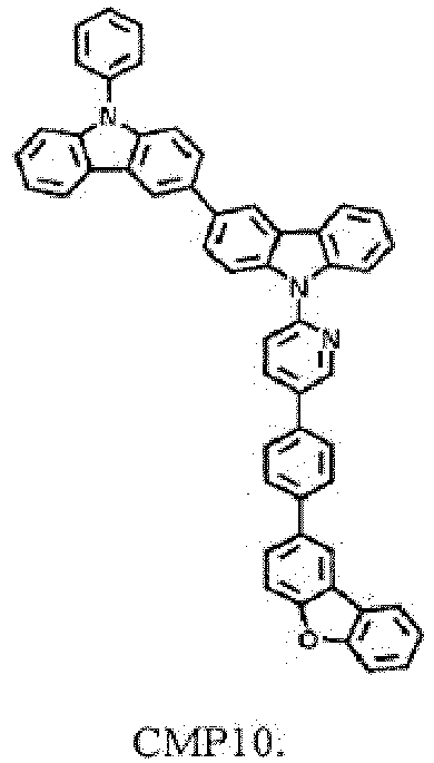
- Dérivé de biscarbazole selon la revendication 1, dans lequel le A1 représente un groupe 1-dibenzofuranyle, un groupe 3-dibenzofuranyle, un groupe 4-dibenzofuranyle, ou un groupe dibenzothiophényle.
- Dérivé de biscarbazole selon la revendication 1 ou 2, dans lequel le groupe dibenzofuranyle représenté par A1 est un groupe 4-dibenzofuranyle, et le groupe dibenzothiophényle représenté par A1 est un groupe 4- dibenzothiophényle.
- Matériau pour un dispositif électroluminescent organique, comprenant le dérivé de biscarbazole selon l'une quelconque des revendications 1 à 3.
- Dispositif électroluminescent organique, comprenant une pluralité de couches de film mince organique incluant une couche émettrice de lumière entre une cathode et une anode, dans lequel au moins l'une de la pluralité de couches de film mince organique comprend le dérivé de biscarbazole selon l'une quelconque des revendications 1 à 3.
- Dispositif électroluminescent organique selon la revendication 5, dans lequel la couche émettrice de lumière comprend le dérivé de biscarbazole comme matériau hôte.
- Dispositif électroluminescent organique selon la revendication 6, dans lequel la couche émettrice de lumière comprend un matériau phosphorescent.
- Dispositif électroluminescent organique selon la revendication 7, dans lequel le matériau phosphorescent comprend un complexe ortho-métallé d'un atome de métal choisi parmi l'iridium (Ir), l'osmium (Os), et le platine (Pt).
- Dispositif électroluminescent organique, comprenant une pluralité de couches de film mince organique incluant une couche émettrice de lumière entre une cathode et une anode, dans lequel la couche émettrice de lumière comprend un dérivé de biscarbazole comme matériau hôte, qui est représenté par l'une quelconque des formules (2) à (4) suivantes :
 A1 représente un groupe dibenzofuranyle ou un groupe dibenzothiophényle ;A2 représente un groupe hydrocarboné aromatique substitué ou non substitué ayant 6 à 30 atomes de carbone de cycle, ou un groupe benzofuranyle substitué ou non substitué, un groupe benzothiophényle substitué ou non substitué, un groupe benzonaphtofuranyle substitué ou non substitué, ou un groupe benzonaphtothiophényle substitué ou non substitué ;Y6 et Y11 représentent chacun C, et Y1, Y2, Y3, Y4, Y5, Y7, Y8, Y9, Y10, Y12, Y13, Y14, Y15, et Y16 représentent chacun indépendamment C(R) ou un atome d'azote, et les R représentent chacun indépendamment un atome d'hydrogène ou un substituant ; etL1 représente un groupe hydrocarboné aromatique divalent substitué ou non substitué ayant 6 à 30 atomes de carbone de cycle, ou un groupe hétérocyclique aromatique divalent substitué ou non substitué ayant 2 à 30 atomes de carbone de cycle ; etL2 représente une liaison simple, un groupe hydrocarboné aromatique divalent substitué ou non substitué ayant 6 à 30 atomes de carbone de cycle, ou un groupe hétérocyclique aromatique divalent substitué ou non substitué ayant 2 à 30 atomes de carbone de cycle ;
 A1 et A2 sont tels que définis dans la formule (2) ;Y7 et Y11 représentent chacun C, et Y1, Y2, Y3, Y4, Y5, Y6, Y8, Y9, Y10, Y12, Y13, Y14, Y15, et Y16 représentent chacun indépendamment C(R) ou un atome d'azote, et les R représentent chacun indépendamment un atome d'hydrogène ou un substituant ;L1 et L2 représentent chacun indépendamment une liaison simple, un groupe hydrocarboné aromatique divalent substitué ou non substitué ayant 6 à 30 atomes de carbone de cycle, ou un groupe hétérocyclique aromatique divalent substitué ou non substitué ayant 2 à 30 atomes de carbone de cycle, etau moins l'un parmi L1 et L2 représente le groupe hydrocarboné aromatique divalent substitué ou non substitué ayant 6 à 30 atomes de carbone de cycle, ou le groupe hétérocyclique aromatique divalent substitué ou non substitué ayant 2 à 30 atomes de carbone de cycle,
 A1 et A2 sont tels que définis dans la formule (2) ;Y7 et Y10 représentent chacun C, et Y1, Y2, Y3, Y4, Y5, Y6, Y8, Y9, Y11, Y12, Y13, Y14, Y15, et Y16 représentent chacun indépendamment C(R) ou un atome d'azote, et les R représentent chacun indépendamment un atome d'hydrogène ou un substituant ;L1 et L2 représentent chacun indépendamment une liaison simple, un groupe hydrocarboné aromatique divalent substitué ou non substitué ayant 6 à 30 atomes de carbone de cycle, ou un groupe hétérocyclique aromatique divalent substitué ou non substitué ayant 2 à 30 atomes de carbone de cycle, etau moins l'un parmi L1 et L2 représente le groupe hydrocarboné aromatique divalent substitué ou non substitué ayant 6 à 30 atomes de carbone de cycle, ou le groupe hétérocyclique aromatique divalent substitué ou non substitué ayant 2 à 30 atomes de carbone de cycle,à condition que :
le groupe hétérocyclique aromatique divalent ayant 2 à 30 atomes de carbone de cycle désigné ci-dessus dans les définitions de L1 et L2 par rapport aux formules (2) à (4) soit choisi parmi un groupe pyrrolyle, un groupe pyrazinyle, un groupe pyridinyle, un groupe indolyle, un groupe isoindolyle, un groupe furyle, un groupe benzofuranyle, un groupe isobenzofuranyle, un groupe dibenzofuranyle, un groupe dibenzothiophényle, un groupe quinolyle, un groupe isoquinolyle, un groupe quinoxalinyle, un groupe phénanthridinyle, un groupe acridinyle, un groupe phénanthrolinyle, un groupe thiényle, et des groupes formés à partir d'un cycle pyridine, d'un cycle pyrazine, d'un cycle pyrimidine, d'un cycle pyridazine, d'un cycle triazine, d'un cycle indole, d'un cycle quinoléine, d'un cycle acridine, d'un cycle pyrrolidine, d'un cycle dioxane, d'un cycle pipéridine, d'un cycle morpholine, d'un cycle pipérazine, d'un cycle furane, d'un cycle thiophène, d'un cycle oxazole, d'un cycle oxadiazole, d'un cycle benzoxazole, d'un cycle thiazole, d'un cycle thiadiazole, d'un cycle benzothiazole, d'un cycle triazole, d'un cycle imidazole, d'un cycle benzimidazole, d'un cycle pyrane, d'un cycle dibenzofurane, et d'un cycle benzo[c]dibenzofurane ; et le dérivé de biscarbazole a seulement deux structures carbazole dans une molécule de celui-ci,
dans lequel la couche émettrice de lumière comprend un matériau phosphorescent qui comprend un complexe ortho-métallé d'un atome de métal choisi parmi l'iridium (Ir), l'osmium (Os), et le platine (Pt) ; et
dans lequel une couche d'injection d'électrons est placée entre la cathode et la couche émettrice de lumière, et la couche d'injection d'électrons comprend un dérivé cyclique contenant de l'azote. - Dispositif électroluminescent organique selon la revendication 9, dans lequel une couche de transport d'électrons est placée entre la cathode et la couche émettrice de lumière, et la couche de transport d'électrons comprend le dérivé de biscarbazole.
- Dispositif électroluminescent organique selon la revendication 10, dans lequel une couche de transport de trous est placée entre l'anode et la couche émettrice de lumière, et la couche de transport de trous comprend le dérivé de biscarbazole.
- Dispositif électroluminescent organique selon la revendication 11, comprenant en outre un dopant donneur d'électrons au niveau d'une interface entre la cathode et la pluralité de couches de film mince organique.
- Dispositif électroluminescent organique selon la revendication 5 ou 6, ledit dispositif étant utilisé pour l'émission de fluorescence.
- Dispositif électroluminescent organique selon la revendication 13, dans lequel une couche d'injection de trous est placée entre l'anode et une couche de transport de trous.
- Dispositif électroluminescent organique selon la revendication 14, dans lequel au moins l'une parmi la couche de transport de trous et la couche d'injection de trous comprend un matériau accepteur.
- Dispositif électroluminescent organique selon l'une quelconque des revendications 13 à 15, dans lequel la couche émettrice de lumière comprend au moins un type choisi parmi un dérivé d'anthracène, un dérivé de fluoranthène, un dérivé de styrylamine, et un dérivé d'arylamine.
- Appareil d'éclairage, comprenant le dispositif électroluminescent organique selon l'une quelconque des revendications 5 à 16.
- Appareil d'affichage, comprenant le dispositif électroluminescent organique selon l'une quelconque des revendications 5 à 16.
Applications Claiming Priority (4)
| Application Number | Priority Date | Filing Date | Title |
|---|---|---|---|
| JP2011024452 | 2011-02-07 | ||
| JP2011229112 | 2011-10-18 | ||
| JP2011229117 | 2011-10-18 | ||
| PCT/JP2012/052640 WO2012108389A1 (fr) | 2011-02-07 | 2012-02-06 | Dérivé de bis-carbazole ainsi qu'élément électroluminescent organique mettant en oeuvre celui-ci |
Publications (3)
| Publication Number | Publication Date |
|---|---|
| EP2674429A1 EP2674429A1 (fr) | 2013-12-18 |
| EP2674429A4 EP2674429A4 (fr) | 2014-07-30 |
| EP2674429B1 true EP2674429B1 (fr) | 2020-12-23 |
Family
ID=46638604
Family Applications (1)
| Application Number | Title | Priority Date | Filing Date |
|---|---|---|---|
| EP12744393.5A Active EP2674429B1 (fr) | 2011-02-07 | 2012-02-06 | Dérivé de biscarbazole ainsi qu'élément électroluminescent organique utilisant celui-ci |
Country Status (7)
| Country | Link |
|---|---|
| US (4) | US8803134B2 (fr) |
| EP (1) | EP2674429B1 (fr) |
| JP (1) | JP5870045B2 (fr) |
| KR (1) | KR101874657B1 (fr) |
| CN (1) | CN103313980B (fr) |
| TW (1) | TWI591154B (fr) |
| WO (1) | WO2012108389A1 (fr) |
Families Citing this family (81)
| Publication number | Priority date | Publication date | Assignee | Title |
|---|---|---|---|---|
| KR101506999B1 (ko) | 2009-11-03 | 2015-03-31 | 제일모직 주식회사 | 유기광전소자용 화합물 및 이를 포함하는 유기광전소자 |
| US8828561B2 (en) | 2009-11-03 | 2014-09-09 | Cheil Industries, Inc. | Compound for organic photoelectric device and organic photoelectric device including the same |
| WO2012108389A1 (fr) | 2011-02-07 | 2012-08-16 | 出光興産株式会社 | Dérivé de bis-carbazole ainsi qu'élément électroluminescent organique mettant en oeuvre celui-ci |
| WO2012108388A1 (fr) | 2011-02-07 | 2012-08-16 | 出光興産株式会社 | Dérivé de bis-carbazole ainsi qu'élément électroluminescent organique mettant en oeuvre celui-ci |
| KR20130025087A (ko) * | 2011-09-01 | 2013-03-11 | 롬엔드하스전자재료코리아유한회사 | 신규한 유기 발광 화합물 및 이를 채용하고 있는 유기 발광 화합물 |
| EP2752902B9 (fr) | 2011-11-22 | 2017-08-30 | Idemitsu Kosan Co., Ltd | Dérivé hétérocyclique aromatique, matière pour élément électroluminescent organique et élément électroluminescent organique |
| JP5898683B2 (ja) | 2011-12-05 | 2016-04-06 | 出光興産株式会社 | 有機エレクトロルミネッセンス素子用材料および有機エレクトロルミネッセンス素子 |
| WO2013102992A1 (fr) * | 2012-01-05 | 2013-07-11 | 出光興産株式会社 | Matériau pour élément organique électroluminescent et élément utilisant ce matériau |
| JPWO2013105206A1 (ja) * | 2012-01-10 | 2015-05-11 | 出光興産株式会社 | 有機エレクトロルミネッセンス素子用材料及びそれを用いた素子 |
| WO2013172835A1 (fr) * | 2012-05-17 | 2013-11-21 | Universal Display Corporation | Matériaux hôtes dérivés du biscarbazole pour région électroluminescente d'oled |
| KR101497138B1 (ko) * | 2012-08-21 | 2015-02-27 | 제일모직 주식회사 | 유기광전자소자 및 이를 포함하는 표시장치 |
| KR102196594B1 (ko) * | 2012-08-30 | 2020-12-30 | 이데미쓰 고산 가부시키가이샤 | 방향족 아민 유도체 및 이것을 이용한 유기 전기발광 소자 |
| WO2014034791A1 (fr) * | 2012-08-31 | 2014-03-06 | 出光興産株式会社 | Élément électroluminescent organique |
| US9577221B2 (en) | 2012-09-26 | 2017-02-21 | Universal Display Corporation | Three stack hybrid white OLED for enhanced efficiency and lifetime |
| WO2014057685A1 (fr) * | 2012-10-11 | 2014-04-17 | 出光興産株式会社 | Élément électroluminescent organique |
| CN104718210B (zh) * | 2012-10-11 | 2018-09-11 | 出光兴产株式会社 | 梯形化合物以及使用其的有机电致发光元件 |
| TWI496327B (zh) * | 2012-11-13 | 2015-08-11 | Nat Univ Tsing Hua | 類燭光有機發光二極體 |
| KR101906591B1 (ko) * | 2012-12-12 | 2018-10-12 | 한국전자통신연구원 | 자발광형 및 반사형 소자를 포함하는 이중모드 화소 및 이를 이용한 이중모드 디스플레이 |
| KR20140087806A (ko) * | 2012-12-31 | 2014-07-09 | 제일모직주식회사 | 유기광전자소자용 화합물, 이를 포함하는 유기발광소자 및 상기 유기발광소자를 포함하는 표시장치 |
| KR101684979B1 (ko) * | 2012-12-31 | 2016-12-09 | 제일모직 주식회사 | 유기광전자소자 및 이를 포함하는 표시장치 |
| KR101820865B1 (ko) | 2013-01-17 | 2018-01-22 | 삼성전자주식회사 | 유기광전자소자용 재료, 이를 포함하는 유기발광소자 및 상기 유기발광소자를 포함하는 표시장치 |
| US9502667B2 (en) * | 2013-01-24 | 2016-11-22 | Idemitsu Kosan Co., Ltd. | Organic electroluminescence |
| KR20160002675A (ko) | 2013-05-02 | 2016-01-08 | 이데미쓰 고산 가부시키가이샤 | 화합물, 유기 전기발광 소자용 재료, 유기 전기발광 소자 및 전자 기기 |
| EP2821459B1 (fr) * | 2013-07-01 | 2017-10-04 | Cheil Industries Inc. | Composition et dispositif optoélectronique organique et dispositif d'affichage |
| KR101566434B1 (ko) * | 2013-07-15 | 2015-11-06 | 삼성디스플레이 주식회사 | 유기 발광 장치 |
| US9508939B2 (en) | 2013-07-23 | 2016-11-29 | Idemitsu Kosan Co., Ltd. | Compound and organic electroluminescent element produced using same |
| KR101649683B1 (ko) * | 2013-09-06 | 2016-08-19 | 제일모직 주식회사 | 유기광전자소자용 조성물, 유기 광전자 소자 및 표시 장치 |
| JP6298608B2 (ja) | 2013-10-03 | 2018-03-20 | 出光興産株式会社 | フルオランテン誘導体、有機エレクトロルミネッセンス素子及び電子機器 |
| JP6446364B2 (ja) * | 2013-10-03 | 2018-12-26 | 出光興産株式会社 | 化合物、これを用いた有機エレクトロルミネッセンス素子用材料、及びこれを用いた有機エレクトロルミネッセンス素子並びに電子機器 |
| KR102171124B1 (ko) * | 2013-10-15 | 2020-10-28 | 덕산네오룩스 주식회사 | 유기전기 소자용 화합물, 이를 이용한 유기전기소자 및 그 전자 장치 |
| CN103664909B (zh) * | 2013-12-10 | 2015-02-25 | 京东方科技集团股份有限公司 | 联咔唑类衍生物及制备方法、应用和有机发光器件 |
| KR101788094B1 (ko) | 2014-01-09 | 2017-10-19 | 제일모직 주식회사 | 유기 화합물, 유기 광전자 소자 및 표시 장치 |
| US10461260B2 (en) * | 2014-06-03 | 2019-10-29 | Universal Display Corporation | Organic electroluminescent materials and devices |
| KR102308903B1 (ko) * | 2014-06-17 | 2021-10-06 | 삼성디스플레이 주식회사 | 유기 발광 소자 |
| KR102430648B1 (ko) * | 2014-09-05 | 2022-08-09 | 롬엔드하스전자재료코리아유한회사 | 정공 전달 재료 및 이를 포함하는 유기 전계 발광 소자 |
| KR102288348B1 (ko) * | 2014-09-24 | 2021-08-11 | 삼성디스플레이 주식회사 | 유기 발광 소자 |
| KR101818581B1 (ko) * | 2014-10-31 | 2018-01-15 | 삼성에스디아이 주식회사 | 유기 광전자 소자 및 표시 장치 |
| KR101829749B1 (ko) | 2014-10-31 | 2018-02-19 | 삼성에스디아이 주식회사 | 유기 광전자 소자용 화합물, 유기 광전자 소자용 조성물, 유기 광전자 소자 및 표시 장치 |
| KR102285386B1 (ko) | 2014-11-03 | 2021-08-04 | 삼성디스플레이 주식회사 | 화합물 및 이를 포함한 유기 발광 소자 |
| KR102352287B1 (ko) | 2014-11-07 | 2022-01-18 | 삼성디스플레이 주식회사 | 유기 발광 소자 |
| KR102385230B1 (ko) | 2014-11-19 | 2022-04-12 | 삼성디스플레이 주식회사 | 유기 발광 소자 |
| KR102363259B1 (ko) | 2014-12-02 | 2022-02-16 | 삼성디스플레이 주식회사 | 유기 발광 소자 |
| KR102363260B1 (ko) * | 2014-12-19 | 2022-02-16 | 삼성디스플레이 주식회사 | 유기 발광 소자 |
| KR102398064B1 (ko) | 2014-12-26 | 2022-05-16 | 삼성디스플레이 주식회사 | 유기 발광 소자 |
| TWI814143B (zh) | 2015-03-09 | 2023-09-01 | 日商半導體能源研究所股份有限公司 | 發光元件、顯示裝置、電子裝置及照明設備 |
| KR102261644B1 (ko) | 2015-03-11 | 2021-06-08 | 삼성디스플레이 주식회사 | 유기 발광 소자 |
| WO2016163372A1 (fr) | 2015-04-08 | 2016-10-13 | 出光興産株式会社 | Composé, matériau pour éléments électroluminescents organiques comprenant ce dernier, et élément électroluminescent organique et dispositif électronique comprenant chacun ce dernier |
| US11322705B2 (en) | 2015-04-17 | 2022-05-03 | Samsung Display Co., Ltd. | Organic light-emitting device |
| CN107710443B (zh) * | 2015-05-11 | 2019-12-17 | 日本放送协会 | 有机薄膜及有机薄膜的制造方法、有机电致发光元件、显示装置、照明装置、有机薄膜太阳能电池、薄膜晶体管、涂料组合物 |
| CN104993066B (zh) * | 2015-05-27 | 2017-11-14 | 京东方科技集团股份有限公司 | 一种oled器件及其制备方法、显示装置 |
| JPWO2016204150A1 (ja) | 2015-06-16 | 2018-04-05 | 出光興産株式会社 | 化合物、有機エレクトロルミネッセンス素子用材料、有機エレクトロルミネッセンス素子及び電子機器 |
| US20170229661A1 (en) | 2015-06-16 | 2017-08-10 | Idemitsu Kosan Co., Ltd. | Compound, material for organic electroluminescence element, organic electroluminescence element, and electronic device |
| EP3680948A3 (fr) | 2015-08-21 | 2020-10-21 | Samsung Display Co., Ltd. | Dispositif électroluminescent organique |
| WO2017056053A1 (fr) | 2015-10-01 | 2017-04-06 | Idemitsu Kosan Co., Ltd. | Groupes benzimidazolo[1,2-a]benzimidazolyle, groupes carbazolyle, groupes benzofuranne ou groupes benzothiophène portant un composé benzimidazolo[1,2-a] benzimidazole pour diodes électroluminescentes organiques |
| EP3150606B1 (fr) | 2015-10-01 | 2019-08-14 | Idemitsu Kosan Co., Ltd. | Benzimidazolo[1,2-a]benzimidazoles avec des groupements benzofurane ou benzothiophène pour des diodes émittant de la lumière |
| US20180269407A1 (en) | 2015-10-01 | 2018-09-20 | Idemitsu Kosan Co., Ltd. | Benzimidazolo[1,2-a]benzimidazole carrying triazine groups for organic light emitting diodes |
| EP3150604B1 (fr) | 2015-10-01 | 2021-07-14 | Idemitsu Kosan Co., Ltd. | Groupes benzimidazolo [1,2-a] benzimidazoles portant des benzimidazolo [1,2-a] benzimidazolyles, groupes carbazolyles, groupes benzofuranes ou benzothiophènes pour diodes électroluminescentes organiques |
| CN108349987A (zh) | 2015-11-04 | 2018-07-31 | 出光兴产株式会社 | 苯并咪唑稠合杂芳族类 |
| KR102399570B1 (ko) | 2015-11-26 | 2022-05-19 | 삼성디스플레이 주식회사 | 유기 발광 소자 |
| US11174258B2 (en) | 2015-12-04 | 2021-11-16 | Idemitsu Kosan Co., Ltd. | Benzimidazolo[1,2-a]benzimidazole derivatives for organic light emitting diodes |
| US20180370981A1 (en) | 2015-12-21 | 2018-12-27 | Idemitsu Kosan Co., Ltd. | Hetero-condensed phenylquinazolines and their use in electronic devices |
| US11910707B2 (en) | 2015-12-23 | 2024-02-20 | Samsung Display Co., Ltd. | Organic light-emitting device |
| KR20170127101A (ko) | 2016-05-10 | 2017-11-21 | 삼성디스플레이 주식회사 | 유기 발광 소자 |
| WO2017221999A1 (fr) | 2016-06-22 | 2017-12-28 | Idemitsu Kosan Co., Ltd. | Benzofuro- et benzothiénoquinolines à substitution spécifique pour diodes électroluminescentes organiques |
| KR20180007617A (ko) * | 2016-07-13 | 2018-01-23 | 삼성에스디아이 주식회사 | 유기 광전자 소자용 조성물, 유기 광전자 소자 및 표시 장치 |
| KR20180010533A (ko) * | 2016-07-21 | 2018-01-31 | 삼성에스디아이 주식회사 | 유기 광전자 소자용 조성물, 유기 광전자 소자 및 표시 장치 |
| TWI589673B (zh) * | 2016-11-03 | 2017-07-01 | 元智大學 | 雙極性材料以及有機發光二極體元件 |
| US11518723B2 (en) * | 2016-11-23 | 2022-12-06 | Guangzhou Chinaray Optoelectronic Materials Ltd. | Fused ring compound, high polymer, mixture, composition and organic electronic component |
| KR20180137772A (ko) * | 2017-06-19 | 2018-12-28 | 삼성에스디아이 주식회사 | 유기 광전자 소자 및 표시 장치 |
| CN108424420B (zh) * | 2017-09-30 | 2021-01-12 | 北京绿人科技有限责任公司 | 含有硅原子的三嗪化合物及其应用和一种有机电致发光器件 |
| EP3466954A1 (fr) | 2017-10-04 | 2019-04-10 | Idemitsu Kosan Co., Ltd. | Phénylquinazolines condensées et pontées avec un hétéroatome |
| CN111954939A (zh) | 2018-03-07 | 2020-11-17 | 株式会社半导体能源研究所 | 发光元件、显示装置、电子设备、有机化合物及照明装置 |
| EP3569605A1 (fr) | 2018-05-18 | 2019-11-20 | Idemitsu Kosan Co., Ltd. | Nouveaux complexes métalliques électroluminescents et dispositif électroluminescent organique les comprenant |
| EP3604477A1 (fr) | 2018-07-30 | 2020-02-05 | Idemitsu Kosan Co., Ltd. | Composé polycyclique, dispositif électroluminescent organique et dispositif électronique |
| EP3608319A1 (fr) | 2018-08-07 | 2020-02-12 | Idemitsu Kosan Co., Ltd. | Azacycles condensés comme dispositif électroluminescent organique et matériaux à utiliser en son sein |
| KR102231624B1 (ko) * | 2018-09-04 | 2021-03-24 | 주식회사 엘지화학 | 유기 발광 소자 |
| EP3643761A1 (fr) | 2018-10-25 | 2020-04-29 | Idemitsu Kosan Co., Ltd. | Composition, matériau pour dispositif électroluminescent organique, film de composition, dispositif d'électroluminescence organique et dispositif électronique |
| CN112851655B (zh) * | 2021-01-07 | 2022-09-02 | 山西华辉光电科技有限公司 | 一种基于咔唑的有机电致发光材料及其在器件中的应用 |
| KR20220153392A (ko) * | 2021-05-11 | 2022-11-18 | 엘티소재주식회사 | 헤테로고리 화합물, 이를 포함하는 유기 발광 소자, 및 유기 발광 소자의 유기물층용 조성물 |
| CN113801109B (zh) * | 2021-08-17 | 2023-01-20 | 南京高光半导体材料有限公司 | 一种含有双咔唑结构的化合物及有机电致发光器件 |
| CN114213314A (zh) * | 2021-12-31 | 2022-03-22 | 维思普新材料(苏州)有限公司 | 一种基于咔唑-9-基-二苯胺类衍生物的有机电致发光材料及其电子器件 |
Citations (2)
| Publication number | Priority date | Publication date | Assignee | Title |
|---|---|---|---|---|
| WO2011162162A1 (fr) * | 2010-06-24 | 2011-12-29 | 東レ株式会社 | Matériau de dispositif électroluminescent et dispositif électroluminescent |
| WO2012087007A1 (fr) * | 2010-12-21 | 2012-06-28 | Rohm And Haas Electronic Materials Korea Ltd. | Nouveaux composés électroluminescents organiques et dispositif électroluminescent organique les utilisant |
Family Cites Families (145)
| Publication number | Priority date | Publication date | Assignee | Title |
|---|---|---|---|---|
| JP2814435B2 (ja) | 1987-03-02 | 1998-10-22 | イーストマン・コダック・カンパニー | 改良薄膜発光帯をもつ電場発光デバイス |
| JPH083547B2 (ja) | 1987-03-24 | 1996-01-17 | 株式会社日立製作所 | 原子炉格納容器の空気調和装置 |
| JP3139321B2 (ja) | 1994-03-31 | 2001-02-26 | 東レ株式会社 | 発光素子 |
| JP3704748B2 (ja) | 1995-06-23 | 2005-10-12 | 東洋インキ製造株式会社 | 有機エレクトロルミネッセンス素子用電子輸送材料およびそれを用いた有機エレクトロルミネッセンス素子 |
| JPH1174084A (ja) | 1997-08-29 | 1999-03-16 | Toray Ind Inc | 発光素子及びその製造方法 |
| JPH11135260A (ja) | 1997-10-28 | 1999-05-21 | Toray Ind Inc | 発光素子 |
| JP3856546B2 (ja) | 1997-11-11 | 2006-12-13 | 三井化学株式会社 | 有機電界発光素子 |
| JP3801326B2 (ja) | 1997-11-18 | 2006-07-26 | 三井化学株式会社 | 有機電界発光素子 |
| JPH11329737A (ja) | 1998-03-13 | 1999-11-30 | Taiho Ind Co Ltd | 有機多層型エレクトロルミネッセンス素子及び有機多層型エレクトロルミネッセンス素子用構造体の合成方法 |
| JP2000173774A (ja) | 1998-12-09 | 2000-06-23 | Sony Corp | 有機電界発光素子 |
| CN1226902C (zh) | 1999-03-23 | 2005-11-09 | 南加利福尼亚大学 | 在有机发光装置中用作磷光掺杂剂的环金属化金属配合物 |
| EP1449238B1 (fr) | 1999-05-13 | 2006-11-02 | The Trustees Of Princeton University | Dispositifs electroluminescents organiques a tres haute performance utilisant l'electrophosphorescence |
| EP3379591A1 (fr) | 1999-12-01 | 2018-09-26 | The Trustees of Princeton University | Complexes de forme l2mx |
| JP4562884B2 (ja) | 2000-08-25 | 2010-10-13 | 出光興産株式会社 | 有機エレクトロルミネッセンス素子 |
| JP4154139B2 (ja) | 2000-09-26 | 2008-09-24 | キヤノン株式会社 | 発光素子 |
| DE10058578C2 (de) | 2000-11-20 | 2002-11-28 | Univ Dresden Tech | Lichtemittierendes Bauelement mit organischen Schichten |
| JP2003133075A (ja) | 2001-07-25 | 2003-05-09 | Toray Ind Inc | 発光素子 |
| JP2003151774A (ja) | 2001-11-14 | 2003-05-23 | Toray Ind Inc | 発光素子 |
| JP4381645B2 (ja) | 2002-02-22 | 2009-12-09 | 出光興産株式会社 | 新規アントラセン化合物およびそれを用いた有機エレクトロルミネッセンス素子 |
| JP4103493B2 (ja) | 2002-08-13 | 2008-06-18 | コニカミノルタホールディングス株式会社 | 有機エレクトロルミネッセンス素子および表示装置 |
| JP4427947B2 (ja) | 2002-11-18 | 2010-03-10 | コニカミノルタホールディングス株式会社 | 有機エレクトロルミネッセンス素子及び表示装置 |
| KR20050085622A (ko) | 2002-12-13 | 2005-08-29 | 코닌클리케 필립스 일렉트로닉스 엔.브이. | 전자발광 디바이스 |
| KR101035818B1 (ko) | 2003-01-24 | 2011-05-20 | 이데미쓰 고산 가부시키가이샤 | 유기 전기발광 소자 |
| US20060073357A1 (en) | 2003-02-12 | 2006-04-06 | Klemens Brunner | Carbazole compounds and use of such compounds in organic electroluminiscent devices |
| JP4305046B2 (ja) | 2003-05-14 | 2009-07-29 | コニカミノルタホールディングス株式会社 | 有機エレクトロルミネッセンス素子、照明装置及び表示装置 |
| KR100569187B1 (ko) | 2003-09-27 | 2006-04-10 | 한국과학기술연구원 | 시클로펜타디엔온으로부터 유도되는 화합물, 이의 제조방법 및 이를 이용한 el 소자 |
| JP4585786B2 (ja) | 2004-04-01 | 2010-11-24 | キヤノン株式会社 | 発光素子及び表示装置 |
| US7329722B2 (en) | 2004-08-30 | 2008-02-12 | Samsung Electronics Co., Ltd | Polymeric charge transport materials having carbazolyl repeating units |
| US20060088728A1 (en) | 2004-10-22 | 2006-04-27 | Raymond Kwong | Arylcarbazoles as hosts in PHOLEDs |
| JP2006143845A (ja) | 2004-11-18 | 2006-06-08 | Konica Minolta Holdings Inc | 有機エレクトロルミネッセンス素子用材料、有機エレクトロルミネッセンス素子、照明装置及び表示装置 |
| CN102603688B (zh) | 2005-05-30 | 2015-11-25 | 西巴特殊化学品控股有限公司 | 电致发光器件 |
| JP5573853B2 (ja) | 2005-09-14 | 2014-08-20 | コニカミノルタ株式会社 | 有機エレクトロルミネッセンス素子 |
| WO2007077810A1 (fr) | 2006-01-05 | 2007-07-12 | Konica Minolta Holdings, Inc. | Dispositif electroluminescent organique, affichage et dispositif d'eclairage |
| JP2007194241A (ja) | 2006-01-17 | 2007-08-02 | Toray Ind Inc | 発光素子 |
| JP2007201193A (ja) | 2006-01-26 | 2007-08-09 | Fuji Xerox Co Ltd | 有機電界発光素子 |
| JP2007201189A (ja) | 2006-01-26 | 2007-08-09 | Fuji Xerox Co Ltd | 有機電界発光素子 |
| JP2007201194A (ja) | 2006-01-26 | 2007-08-09 | Fuji Xerox Co Ltd | 有機電界発光素子 |
| EP2615153B1 (fr) | 2006-03-23 | 2017-03-01 | Konica Minolta Holdings, Inc. | Dispositif électroluminescent organique, affichage et dispositif d'éclairage |
| JP5055818B2 (ja) * | 2006-04-19 | 2012-10-24 | コニカミノルタホールディングス株式会社 | 有機エレクトロルミネッセンス素子材料、有機エレクトロルミネッセンス素子、表示装置及び照明装置 |
| JP5589251B2 (ja) | 2006-09-21 | 2014-09-17 | コニカミノルタ株式会社 | 有機エレクトロルミネッセンス素子材料 |
| JP2008135498A (ja) | 2006-11-28 | 2008-06-12 | Toray Ind Inc | 発光素子 |
| WO2008072596A1 (fr) | 2006-12-13 | 2008-06-19 | Konica Minolta Holdings, Inc. | Dispositif électroluminescent organique, dispositif d'affichage et d'éclairage |
| JP5194456B2 (ja) | 2007-01-23 | 2013-05-08 | コニカミノルタホールディングス株式会社 | 有機エレクトロルミネッセンス素子の製造方法及び照明装置の製造方法 |
| US7723722B2 (en) | 2007-03-23 | 2010-05-25 | Semiconductor Energy Laboratory Co., Ltd. | Organic compound, anthracene derivative, and light-emitting element, light-emitting device, and electronic device using anthracene derivative |
| JP5564942B2 (ja) | 2007-05-16 | 2014-08-06 | コニカミノルタ株式会社 | 有機エレクトロルミネッセンス素子、表示装置及び照明装置 |
| JP4915279B2 (ja) | 2007-05-23 | 2012-04-11 | 東レ株式会社 | 発光素子 |
| US8080658B2 (en) | 2007-07-10 | 2011-12-20 | Idemitsu Kosan Co., Ltd. | Material for organic electroluminescent element and organic electroluminescent element employing the same |
| US7968213B2 (en) * | 2007-07-10 | 2011-06-28 | Idemitsu Kosan Co., Ltd. | Material for organic electroluminescence device and organic electroluminescence device utilizing the same |
| JP2009028943A (ja) | 2007-07-25 | 2009-02-12 | Hideo Hamada | 転写印刷シート |
| CN101126020B (zh) | 2007-08-03 | 2012-11-28 | 深圳大学 | 一类基于1,3,6,8-四芳基-9-烷基取代咔唑衍生物及在发光二极管中的应用 |
| JP5186843B2 (ja) | 2007-08-30 | 2013-04-24 | コニカミノルタホールディングス株式会社 | 有機エレクトロルミネッセンス素子、照明装置及び表示装置 |
| KR20090028943A (ko) | 2007-09-17 | 2009-03-20 | (주)루디스 | 정공주입층/정공수송층 물질 및 이를 포함하는유기전계발광소자 |
| TWI524567B (zh) | 2007-09-27 | 2016-03-01 | 半導體能源研究所股份有限公司 | 發光元件,照明裝置,發光裝置,與電子裝置 |
| US8040047B2 (en) | 2007-10-19 | 2011-10-18 | Semiconductor Energy Laboratory Co., Ltd. | Light-emitting device |
| WO2009060780A1 (fr) | 2007-11-08 | 2009-05-14 | Konica Minolta Holdings, Inc. | Elément électroluminescent organique, dispositif d'affichage, et système d'éclairage |
| JP5018891B2 (ja) * | 2007-11-08 | 2012-09-05 | コニカミノルタホールディングス株式会社 | 有機エレクトロルミネッセンス素子材料、有機エレクトロルミネッセンス素子、表示装置及び照明装置 |
| WO2009060742A1 (fr) | 2007-11-08 | 2009-05-14 | Konica Minolta Holdings, Inc. | Dispositif électroluminescent organique, dispositif d'affichage et dispositif d'éclairage |
| JPWO2009084413A1 (ja) | 2007-12-28 | 2011-05-19 | コニカミノルタホールディングス株式会社 | 有機エレクトロルミネッセンス素子、及び有機エレクトロルミネッセンス素子の製造方法 |
| KR101587867B1 (ko) | 2008-03-18 | 2016-01-22 | 가부시키가이샤 한도오따이 에네루기 켄큐쇼 | 발광소자, 발광장치 및 전자기기 |
| JP4830126B2 (ja) | 2008-03-22 | 2011-12-07 | コニカミノルタホールディングス株式会社 | 有機エレクトロルミネッセンス素子及び表示装置 |
| JP4830127B2 (ja) | 2008-03-22 | 2011-12-07 | コニカミノルタホールディングス株式会社 | 有機エレクトロルミネッセンス素子及び表示装置 |
| JP2009267257A (ja) | 2008-04-28 | 2009-11-12 | Idemitsu Kosan Co Ltd | 有機エレクトロルミネッセンス素子用材料及びそれを用いた有機エレクトロルミネッセンス素子 |
| JP2009267255A (ja) | 2008-04-28 | 2009-11-12 | Idemitsu Kosan Co Ltd | 有機エレクトロルミネッセンス素子用材料及びそれを用いた有機エレクトロルミネッセンス素子 |
| EP2479234B1 (fr) | 2008-05-13 | 2017-06-21 | Konica Minolta Holdings, Inc. | Élément électroluminescent organique, dispositif d'affichage et dispositif d'éclairage |
| EP2120275A3 (fr) | 2008-05-16 | 2012-08-22 | Semiconductor Energy Laboratory Co, Ltd. | Élément électroluminescent, appareil d'éclairage, dispositif électroluminescent, appareil électronique et affichage |
| EP2256176A1 (fr) | 2008-06-25 | 2010-12-01 | Gracel Display Inc. | Nouveaux composés électroluminescents organiques et dispositif électroluminescent organique les utilisant |
| JP5699603B2 (ja) | 2008-07-07 | 2015-04-15 | コニカミノルタ株式会社 | 有機エレクトロルミネッセンス素子、表示装置及び照明装置 |
| WO2010004877A1 (fr) * | 2008-07-10 | 2010-01-14 | コニカミノルタホールディングス株式会社 | Élément électroluminescent organique, dispositif d'affichage et dispositif d'éclairage |
| WO2010044342A1 (fr) | 2008-10-15 | 2010-04-22 | コニカミノルタホールディングス株式会社 | Élément électroluminescent organique, procédé de fabrication d'élément électroluminescent organique, élément électroluminescent organique blanc, dispositif d'affichage et dispositif d'éclairage |
| KR20100048210A (ko) | 2008-10-30 | 2010-05-11 | 다우어드밴스드디스플레이머티리얼 유한회사 | 신규한 유기 발광 화합물 및 이를 포함하는 유기 발광 소자 |
| JP5493333B2 (ja) | 2008-11-05 | 2014-05-14 | コニカミノルタ株式会社 | 有機エレクトロルミネッセンス素子、白色有機エレクトロルミネッセンス素子、表示装置及び照明装置 |
| JP5707665B2 (ja) | 2008-12-03 | 2015-04-30 | コニカミノルタ株式会社 | 有機エレクトロルミネッセンス素子、該素子を備えた照明装置及び表示装置 |
| EP2200407B1 (fr) | 2008-12-17 | 2017-11-22 | Semiconductor Energy Laboratory Co., Ltd. | Élément électroluminescent, dispositif électroluminescent, et dispositif électronique |
| US8581237B2 (en) | 2008-12-17 | 2013-11-12 | Semiconductor Energy Laboratory Co., Ltd. | Light-emitting element |
| KR20100079458A (ko) | 2008-12-31 | 2010-07-08 | 덕산하이메탈(주) | 비스-카바졸 화합물 및 이를 이용한 유기전기소자, 그 단말 |
| WO2010087222A1 (fr) | 2009-01-28 | 2010-08-05 | コニカミノルタホールディングス株式会社 | Élément électroluminescent organique, dispositif d'affichage et dispositif d'éclairage. |
| JP5541167B2 (ja) | 2009-02-06 | 2014-07-09 | コニカミノルタ株式会社 | 有機エレクトロルミネッセンス素子、該素子を備えた照明装置及び表示装置 |
| KR20110117168A (ko) * | 2009-02-18 | 2011-10-26 | 이데미쓰 고산 가부시키가이샤 | 방향족 아민 유도체 및 유기 전기발광 소자 |
| KR101170666B1 (ko) | 2009-03-03 | 2012-08-07 | 덕산하이메탈(주) | 비스카바졸 화합물 및 이를 이용한 유기전기소자, 그 단말 |
| JP5607959B2 (ja) | 2009-03-20 | 2014-10-15 | 株式会社半導体エネルギー研究所 | カルバゾール誘導体、発光素子、発光装置および電子機器 |
| JP5182225B2 (ja) | 2009-05-29 | 2013-04-17 | コニカミノルタホールディングス株式会社 | 有機エレクトロルミネッセンス素子の製造方法 |
| JP5499890B2 (ja) | 2009-08-05 | 2014-05-21 | コニカミノルタ株式会社 | 有機エレクトロルミネッセンス素子、及びその製造方法 |
| KR101431644B1 (ko) | 2009-08-10 | 2014-08-21 | 롬엔드하스전자재료코리아유한회사 | 신규한 유기 발광 화합물 및 이를 포함하는 유기 전계 발광 소자 |
| US9732036B2 (en) | 2009-08-28 | 2017-08-15 | Hodogaya Chemical Co., Ltd. | Compound having carbazole ring structure, and organic electroluminescent device |
| US8378339B2 (en) | 2009-09-11 | 2013-02-19 | Fujifilm Corporation | Photoelectric conversion device, production method thereof, photosensor, imaging device and their drive methods |
| WO2011037429A2 (fr) | 2009-09-28 | 2011-03-31 | 덕산하이메탈(주) | Composés ayant des dérivés hétérocycliques à cycle aryle condensé de 5 chaînons, dispositif électronique organique utilisant les composés, et terminal comprenant le dispositif électronique organique |
| JP5568943B2 (ja) | 2009-10-14 | 2014-08-13 | コニカミノルタ株式会社 | 有機エレクトロルミネッセンス素子、及び照明装置 |
| KR20110043270A (ko) | 2009-10-21 | 2011-04-27 | (주)씨에스엘쏠라 | 유기발광화합물 및 이를 구비한 유기발광소자 |
| KR101869670B1 (ko) | 2009-10-23 | 2018-06-20 | 호도가야 가가쿠 고교 가부시키가이샤 | 유기 일렉트로 루미네센스 소자 |
| EP2492985A4 (fr) | 2009-10-23 | 2017-03-29 | Hodogaya Chemical Co., Ltd. | Élément électroluminescent organique |
| KR101506999B1 (ko) | 2009-11-03 | 2015-03-31 | 제일모직 주식회사 | 유기광전소자용 화합물 및 이를 포함하는 유기광전소자 |
| US8828561B2 (en) | 2009-11-03 | 2014-09-09 | Cheil Industries, Inc. | Compound for organic photoelectric device and organic photoelectric device including the same |
| DE102009053382A1 (de) | 2009-11-14 | 2011-05-19 | Merck Patent Gmbh | Materialien für elektronische Vorrichtungen |
| CN102939674B (zh) | 2009-12-28 | 2017-02-08 | 新日铁住金化学株式会社 | 有机场致发光元件 |
| KR101183722B1 (ko) | 2009-12-30 | 2012-09-17 | 주식회사 두산 | 트리페닐렌계 화합물 및 이를 포함하는 유기 전계 발광 소자 |
| KR20110088898A (ko) | 2010-01-29 | 2011-08-04 | 주식회사 이엘엠 | 유기 전기 발광 조성물 및 이를 포함하는 유기 전기 발광 소자 |
| DE102010010481A1 (de) | 2010-03-06 | 2011-09-08 | Merck Patent Gmbh | Organische Elektrolumineszenzvorrichtung |
| WO2011122133A1 (fr) | 2010-03-31 | 2011-10-06 | 出光興産株式会社 | Substance pour élément électroluminescent organique, et élément électroluminescent organique l'utilisant |
| KR101867105B1 (ko) * | 2010-03-31 | 2018-06-12 | 이데미쓰 고산 가부시키가이샤 | 유기 전기발광 소자용 재료 및 그것을 이용한 유기 전기발광 소자 |
| CN104592206B (zh) | 2010-04-20 | 2019-12-31 | 出光兴产株式会社 | 双咔唑衍生物、有机电致发光元件用材料及使用其的有机电致发光元件 |
| US8227801B2 (en) | 2010-04-26 | 2012-07-24 | Universal Display Corporation | Bicarbzole containing compounds for OLEDs |
| KR20110122051A (ko) | 2010-05-03 | 2011-11-09 | 제일모직주식회사 | 유기광전소자용 화합물 및 이를 포함하는 유기광전소자 |
| KR101244599B1 (ko) | 2010-05-28 | 2013-03-25 | 주식회사 두산 | 바이폴라 트리페닐렌계 화합물 및 이를 포함하는 유기 전계 발광 소자 |
| KR101288567B1 (ko) | 2010-06-01 | 2013-07-22 | 제일모직주식회사 | 유기광전소자용 화합물 및 이를 포함하는 유기광전소자 |
| JP2013201153A (ja) | 2010-06-08 | 2013-10-03 | Idemitsu Kosan Co Ltd | 有機エレクトロルミネッセンス素子 |
| JP2013200939A (ja) | 2010-06-08 | 2013-10-03 | Idemitsu Kosan Co Ltd | 有機エレクトロルミネッセンス素子 |
| US9142792B2 (en) | 2010-06-18 | 2015-09-22 | Basf Se | Organic electronic devices comprising a layer comprising at least one metal organic compound and at least one metal oxide |
| KR101877580B1 (ko) | 2010-06-18 | 2018-08-09 | 유디씨 아일랜드 리미티드 | 디벤조푸란 화합물 및 8-히드록시퀴놀리노레이토 알칼리 토금속 또는 알칼리 금속 착물의 층을 포함하는 유기 전자 소자 |
| JP5621844B2 (ja) | 2010-06-18 | 2014-11-12 | コニカミノルタ株式会社 | 有機エレクトロルミネッセンス素子及び有機エレクトロルミネッセンス素子の製造方法 |
| KR101125683B1 (ko) | 2010-06-21 | 2012-03-27 | 주식회사 이엘엠 | 유기 전기 발광 조성물 및 이를 포함하는 유기 전기 발광 소자 |
| TWI486332B (zh) | 2010-06-30 | 2015-06-01 | Hodogaya Chemical Co Ltd | 具有咔唑環構造之化合物及有機電致發光元件 |
| EP2595208A1 (fr) | 2010-07-13 | 2013-05-22 | Toray Industries, Inc. | Elément électroluminescent |
| JP2012023127A (ja) | 2010-07-13 | 2012-02-02 | Konica Minolta Holdings Inc | 有機エレクトロルミネッセンス素子、その製造方法、及び照明装置 |
| US20140054564A1 (en) | 2010-07-30 | 2014-02-27 | Rohm And Haas Electronic Materials Korea Ltd. | Electroluminescent device using electroluminescent compound as luminescent material |
| KR102004629B1 (ko) | 2010-08-20 | 2019-07-26 | 유니버셜 디스플레이 코포레이션 | Oled를 위한 바이카르바졸 화합물 |
| EP2617712A4 (fr) * | 2010-08-31 | 2014-02-19 | Idemitsu Kosan Co | Dérivé hétérocyclique aromatique contenant de l'azote et dispositif organique d'électroluminescence utilisant ce dernier |
| KR101477614B1 (ko) | 2010-09-17 | 2014-12-31 | 롬엔드하스전자재료코리아유한회사 | 신규한 유기 발광 화합물 및 이를 채용하고 있는 유기 전계 발광 소자 |
| US20120273766A1 (en) | 2010-10-12 | 2012-11-01 | Idemitsu Kosan Co., Ltd. | Aromatic heterocyclic derivative and organic electroluminescence device using the same |
| JP5920222B2 (ja) | 2010-11-11 | 2016-05-18 | コニカミノルタ株式会社 | 有機エレクトロルミネッセンス素子、その製造方法、照明装置、表示装置及び発光ドーパント材料の前駆体 |
| US9324950B2 (en) | 2010-11-22 | 2016-04-26 | Idemitsu Kosan Co., Ltd. | Organic electroluminescence device |
| US20120126205A1 (en) | 2010-11-22 | 2012-05-24 | Idemitsu Kosan Co., Ltd. | Organic electroluminescence device |
| KR101423174B1 (ko) | 2010-12-01 | 2014-07-25 | 제일모직 주식회사 | 유기광전소자용 화합물 및 이를 포함하는 유기광전소자 |
| WO2012077714A1 (fr) | 2010-12-09 | 2012-06-14 | コニカミノルタホールディングス株式会社 | Élément électroluminescent organique et dispositif d'éclairage |
| US9705091B2 (en) | 2010-12-20 | 2017-07-11 | Idemitsu Kosan Co., Ltd. | Aromatic heterocycle derivative and organic electroluminescent element using same |
| EP2660890A4 (fr) * | 2010-12-28 | 2014-05-21 | Idemitsu Kosan Co | Matériau pour éléments électroluminescents organiques et élément électroluminescent organique utilisant ledit matériau |
| KR101870471B1 (ko) | 2011-01-20 | 2018-06-22 | 이데미쓰 고산 가부시키가이샤 | 유기 일렉트로 루미네선스 소자 |
| WO2012108388A1 (fr) | 2011-02-07 | 2012-08-16 | 出光興産株式会社 | Dérivé de bis-carbazole ainsi qu'élément électroluminescent organique mettant en oeuvre celui-ci |
| WO2012108389A1 (fr) | 2011-02-07 | 2012-08-16 | 出光興産株式会社 | Dérivé de bis-carbazole ainsi qu'élément électroluminescent organique mettant en oeuvre celui-ci |
| WO2013084885A1 (fr) | 2011-12-05 | 2013-06-13 | 出光興産株式会社 | Élément électroluminescent organique |
| JP5898683B2 (ja) | 2011-12-05 | 2016-04-06 | 出光興産株式会社 | 有機エレクトロルミネッセンス素子用材料および有機エレクトロルミネッセンス素子 |
| US9530969B2 (en) | 2011-12-05 | 2016-12-27 | Idemitsu Kosan Co., Ltd. | Material for organic electroluminescence device and organic electroluminescence device |
| US9130174B2 (en) | 2012-02-29 | 2015-09-08 | Idemitsu Kosan Co., Ltd. | Material for organic electroluminescence device and organic electroluminescence device |
| JP2015524610A (ja) | 2012-07-04 | 2015-08-24 | サムスン エスディアイ カンパニー,リミテッド | 有機発光素子用組成物、これを含む有機発光層および有機発光素子 |
| KR102048035B1 (ko) | 2013-06-03 | 2019-11-25 | 덕산네오룩스 주식회사 | 유기전기 소자용 화합물을 이용한 유기전기소자 및 그 전자 장치 |
| US10840454B2 (en) | 2013-06-14 | 2020-11-17 | Samsung Display Co., Ltd. | Organic light-emitting devices |
| KR102054162B1 (ko) | 2013-06-26 | 2020-01-22 | 덕산네오룩스 주식회사 | 유기전기 소자용 화합물을 이용한 유기전기소자 및 그 전자 장치 |
| KR102108454B1 (ko) | 2013-07-08 | 2020-05-26 | 덕산네오룩스 주식회사 | 유기전기 소자용 화합물을 이용한 유기전기소자 및 그 전자 장치 |
| KR102054159B1 (ko) | 2013-07-09 | 2019-12-10 | 덕산네오룩스 주식회사 | 유기전기 소자용 화합물을 이용한 유기전기소자 및 그 전자 장치 |
| KR102137429B1 (ko) | 2013-07-11 | 2020-07-24 | 덕산네오룩스 주식회사 | 유기전기 소자용 화합물을 이용한 유기전기소자 및 그 전자 장치 |
| KR20150010580A (ko) | 2013-07-18 | 2015-01-28 | 삼성디스플레이 주식회사 | 유기 일렉트로루미네센스 소자용 재료 및 이를 사용한 유기 일렉트로루미네센스 소자 |
| KR102116496B1 (ko) | 2013-08-26 | 2020-05-29 | 삼성디스플레이 주식회사 | 유기 발광 소자 |
| US20160204352A1 (en) | 2013-08-27 | 2016-07-14 | Hodogaya Chemical Co., Ltd. | Compound having triphenylene ring structure, and organic electroluminescent device |
| KR102180085B1 (ko) | 2013-09-12 | 2020-11-17 | 덕산네오룩스 주식회사 | 유기전기 소자용 화합물을 이용한 유기전기소자 및 그 전자장치 |
| JP2015065248A (ja) | 2013-09-24 | 2015-04-09 | 出光興産株式会社 | 有機エレクトロルミネッセンス素子および電子機器 |
| JP6298608B2 (ja) | 2013-10-03 | 2018-03-20 | 出光興産株式会社 | フルオランテン誘導体、有機エレクトロルミネッセンス素子及び電子機器 |
-
2012
- 2012-02-06 WO PCT/JP2012/052640 patent/WO2012108389A1/fr active Application Filing
- 2012-02-06 CN CN201280004503.5A patent/CN103313980B/zh active Active
- 2012-02-06 KR KR1020137014075A patent/KR101874657B1/ko active IP Right Grant
- 2012-02-06 EP EP12744393.5A patent/EP2674429B1/fr active Active
- 2012-02-06 US US13/366,891 patent/US8803134B2/en active Active
- 2012-02-06 JP JP2012556880A patent/JP5870045B2/ja active Active
- 2012-02-06 TW TW101103834A patent/TWI591154B/zh active
-
2014
- 2014-06-30 US US14/318,738 patent/US9373802B2/en active Active
-
2016
- 2016-04-27 US US15/139,508 patent/US9818958B2/en active Active
-
2017
- 2017-10-09 US US15/727,667 patent/US10230057B2/en active Active
Patent Citations (2)
| Publication number | Priority date | Publication date | Assignee | Title |
|---|---|---|---|---|
| WO2011162162A1 (fr) * | 2010-06-24 | 2011-12-29 | 東レ株式会社 | Matériau de dispositif électroluminescent et dispositif électroluminescent |
| WO2012087007A1 (fr) * | 2010-12-21 | 2012-06-28 | Rohm And Haas Electronic Materials Korea Ltd. | Nouveaux composés électroluminescents organiques et dispositif électroluminescent organique les utilisant |
Also Published As
| Publication number | Publication date |
|---|---|
| JPWO2012108389A1 (ja) | 2014-07-03 |
| US20160240795A1 (en) | 2016-08-18 |
| KR20140000259A (ko) | 2014-01-02 |
| US8803134B2 (en) | 2014-08-12 |
| US9373802B2 (en) | 2016-06-21 |
| US20180047917A1 (en) | 2018-02-15 |
| JP5870045B2 (ja) | 2016-02-24 |
| CN103313980B (zh) | 2017-04-19 |
| TW201237140A (en) | 2012-09-16 |
| CN103313980A (zh) | 2013-09-18 |
| WO2012108389A1 (fr) | 2012-08-16 |
| EP2674429A4 (fr) | 2014-07-30 |
| US20140312331A1 (en) | 2014-10-23 |
| US9818958B2 (en) | 2017-11-14 |
| US20120223295A1 (en) | 2012-09-06 |
| US10230057B2 (en) | 2019-03-12 |
| KR101874657B1 (ko) | 2018-07-04 |
| TWI591154B (zh) | 2017-07-11 |
| EP2674429A1 (fr) | 2013-12-18 |
Similar Documents
| Publication | Publication Date | Title |
|---|---|---|
| US10230057B2 (en) | Biscarbazole derivatives and organic electroluminescence device employing the same | |
| EP2674418B1 (fr) | Dérivé de biscarbazole ainsi qu'élément électroluminescent organique utilisant celui-ci | |
| JP6195828B2 (ja) | 有機エレクトロルミネッセンス素子用材料、及びそれを用いた有機エレクトロルミネッセンス素子 | |
| EP3010055B1 (fr) | Matière pour éléments électroluminescents organiques, élément électroluminescent organique utilisant cette matière et dispositif électronique | |
| EP2790239B1 (fr) | Matériau pour élément électroluminescent organique et élément électroluminescent organique | |
| US9966541B2 (en) | Biscarbazole derivative host materials and green emitter for OLED emissive region | |
| CN104837834B (zh) | 芳香族胺衍生物和有机电致发光元件 | |
| EP2489664A1 (fr) | Composé aromatique contenant du fluorène, matériau pour élément électroluminescent organique, et élément électroluminescent organique utilisant un tel matériau | |
| JP5756288B2 (ja) | 縮合多環化合物、有機エレクトロルミネッセンス素子用材料、及びそれを用いた有機エレクトロルミネッセンス素子 | |
| KR20140037854A (ko) | 유기 전기발광 소자 | |
| EP3040335B1 (fr) | Composé, élément électroluminescent organique et dispositif électronique | |
| WO2014051004A1 (fr) | Matériau pour éléments électroluminescents organiques, et élément électroluminescent organique | |
| WO2014054263A1 (fr) | Matériau destiné à un élément organique électroluminescent, et élément organique électroluminescent produit en utilisant ledit matériau | |
| WO2014050093A1 (fr) | Matériau destiné à un élément électroluminescent organique, et élément électroluminescent organique produit en utilisant celui-ci | |
| JP2014196251A (ja) | ヘテロアレーン誘導体、有機エレクトロルミネッセンス素子用材料、及び有機エレクトロルミネッセンス素子 | |
| JP2014196252A (ja) | ヘテロアレーン誘導体、有機エレクトロルミネッセンス素子用材料、及び有機エレクトロルミネッセンス素子 |
Legal Events
| Date | Code | Title | Description |
|---|---|---|---|
| PUAI | Public reference made under article 153(3) epc to a published international application that has entered the european phase |
Free format text: ORIGINAL CODE: 0009012 |
|
| 17P | Request for examination filed |
Effective date: 20130626 |
|
| AK | Designated contracting states |
Kind code of ref document: A1 Designated state(s): AL AT BE BG CH CY CZ DE DK EE ES FI FR GB GR HR HU IE IS IT LI LT LU LV MC MK MT NL NO PL PT RO RS SE SI SK SM TR |
|
| DAX | Request for extension of the european patent (deleted) | ||
| A4 | Supplementary search report drawn up and despatched |
Effective date: 20140630 |
|
| RIC1 | Information provided on ipc code assigned before grant |
Ipc: C07D 405/14 20060101AFI20140624BHEP Ipc: C09K 11/06 20060101ALI20140624BHEP Ipc: H01L 51/50 20060101ALI20140624BHEP Ipc: H01L 51/00 20060101ALI20140624BHEP |
|
| 17Q | First examination report despatched |
Effective date: 20160405 |
|
| STAA | Information on the status of an ep patent application or granted ep patent |
Free format text: STATUS: EXAMINATION IS IN PROGRESS |
|
| GRAP | Despatch of communication of intention to grant a patent |
Free format text: ORIGINAL CODE: EPIDOSNIGR1 |
|
| STAA | Information on the status of an ep patent application or granted ep patent |
Free format text: STATUS: GRANT OF PATENT IS INTENDED |
|
| INTG | Intention to grant announced |
Effective date: 20200708 |
|
| GRAS | Grant fee paid |
Free format text: ORIGINAL CODE: EPIDOSNIGR3 |
|
| GRAA | (expected) grant |
Free format text: ORIGINAL CODE: 0009210 |
|
| STAA | Information on the status of an ep patent application or granted ep patent |
Free format text: STATUS: THE PATENT HAS BEEN GRANTED |
|
| AK | Designated contracting states |
Kind code of ref document: B1 Designated state(s): AL AT BE BG CH CY CZ DE DK EE ES FI FR GB GR HR HU IE IS IT LI LT LU LV MC MK MT NL NO PL PT RO RS SE SI SK SM TR |
|
| REG | Reference to a national code |
Ref country code: GB Ref legal event code: FG4D |
|
| REG | Reference to a national code |
Ref country code: DE Ref legal event code: R096 Ref document number: 602012073840 Country of ref document: DE |
|
| REG | Reference to a national code |
Ref country code: AT Ref legal event code: REF Ref document number: 1347598 Country of ref document: AT Kind code of ref document: T Effective date: 20210115 |
|
| REG | Reference to a national code |
Ref country code: IE Ref legal event code: FG4D |
|
| PG25 | Lapsed in a contracting state [announced via postgrant information from national office to epo] |
Ref country code: GR Free format text: LAPSE BECAUSE OF FAILURE TO SUBMIT A TRANSLATION OF THE DESCRIPTION OR TO PAY THE FEE WITHIN THE PRESCRIBED TIME-LIMIT Effective date: 20210324 Ref country code: FI Free format text: LAPSE BECAUSE OF FAILURE TO SUBMIT A TRANSLATION OF THE DESCRIPTION OR TO PAY THE FEE WITHIN THE PRESCRIBED TIME-LIMIT Effective date: 20201223 Ref country code: RS Free format text: LAPSE BECAUSE OF FAILURE TO SUBMIT A TRANSLATION OF THE DESCRIPTION OR TO PAY THE FEE WITHIN THE PRESCRIBED TIME-LIMIT Effective date: 20201223 Ref country code: NO Free format text: LAPSE BECAUSE OF FAILURE TO SUBMIT A TRANSLATION OF THE DESCRIPTION OR TO PAY THE FEE WITHIN THE PRESCRIBED TIME-LIMIT Effective date: 20210323 |
|
| REG | Reference to a national code |
Ref country code: AT Ref legal event code: MK05 Ref document number: 1347598 Country of ref document: AT Kind code of ref document: T Effective date: 20201223 |
|
| REG | Reference to a national code |
Ref country code: NL Ref legal event code: MP Effective date: 20201223 |
|
| PG25 | Lapsed in a contracting state [announced via postgrant information from national office to epo] |
Ref country code: BG Free format text: LAPSE BECAUSE OF FAILURE TO SUBMIT A TRANSLATION OF THE DESCRIPTION OR TO PAY THE FEE WITHIN THE PRESCRIBED TIME-LIMIT Effective date: 20210323 Ref country code: SE Free format text: LAPSE BECAUSE OF FAILURE TO SUBMIT A TRANSLATION OF THE DESCRIPTION OR TO PAY THE FEE WITHIN THE PRESCRIBED TIME-LIMIT Effective date: 20201223 Ref country code: LV Free format text: LAPSE BECAUSE OF FAILURE TO SUBMIT A TRANSLATION OF THE DESCRIPTION OR TO PAY THE FEE WITHIN THE PRESCRIBED TIME-LIMIT Effective date: 20201223 |
|
| PG25 | Lapsed in a contracting state [announced via postgrant information from national office to epo] |
Ref country code: NL Free format text: LAPSE BECAUSE OF FAILURE TO SUBMIT A TRANSLATION OF THE DESCRIPTION OR TO PAY THE FEE WITHIN THE PRESCRIBED TIME-LIMIT Effective date: 20201223 Ref country code: HR Free format text: LAPSE BECAUSE OF FAILURE TO SUBMIT A TRANSLATION OF THE DESCRIPTION OR TO PAY THE FEE WITHIN THE PRESCRIBED TIME-LIMIT Effective date: 20201223 |
|
| REG | Reference to a national code |
Ref country code: LT Ref legal event code: MG9D |
|
| PG25 | Lapsed in a contracting state [announced via postgrant information from national office to epo] |
Ref country code: LT Free format text: LAPSE BECAUSE OF FAILURE TO SUBMIT A TRANSLATION OF THE DESCRIPTION OR TO PAY THE FEE WITHIN THE PRESCRIBED TIME-LIMIT Effective date: 20201223 Ref country code: PT Free format text: LAPSE BECAUSE OF FAILURE TO SUBMIT A TRANSLATION OF THE DESCRIPTION OR TO PAY THE FEE WITHIN THE PRESCRIBED TIME-LIMIT Effective date: 20210423 Ref country code: SK Free format text: LAPSE BECAUSE OF FAILURE TO SUBMIT A TRANSLATION OF THE DESCRIPTION OR TO PAY THE FEE WITHIN THE PRESCRIBED TIME-LIMIT Effective date: 20201223 Ref country code: RO Free format text: LAPSE BECAUSE OF FAILURE TO SUBMIT A TRANSLATION OF THE DESCRIPTION OR TO PAY THE FEE WITHIN THE PRESCRIBED TIME-LIMIT Effective date: 20201223 Ref country code: SM Free format text: LAPSE BECAUSE OF FAILURE TO SUBMIT A TRANSLATION OF THE DESCRIPTION OR TO PAY THE FEE WITHIN THE PRESCRIBED TIME-LIMIT Effective date: 20201223 Ref country code: CZ Free format text: LAPSE BECAUSE OF FAILURE TO SUBMIT A TRANSLATION OF THE DESCRIPTION OR TO PAY THE FEE WITHIN THE PRESCRIBED TIME-LIMIT Effective date: 20201223 Ref country code: EE Free format text: LAPSE BECAUSE OF FAILURE TO SUBMIT A TRANSLATION OF THE DESCRIPTION OR TO PAY THE FEE WITHIN THE PRESCRIBED TIME-LIMIT Effective date: 20201223 |
|
| PG25 | Lapsed in a contracting state [announced via postgrant information from national office to epo] |
Ref country code: PL Free format text: LAPSE BECAUSE OF FAILURE TO SUBMIT A TRANSLATION OF THE DESCRIPTION OR TO PAY THE FEE WITHIN THE PRESCRIBED TIME-LIMIT Effective date: 20201223 Ref country code: AT Free format text: LAPSE BECAUSE OF FAILURE TO SUBMIT A TRANSLATION OF THE DESCRIPTION OR TO PAY THE FEE WITHIN THE PRESCRIBED TIME-LIMIT Effective date: 20201223 |
|
| REG | Reference to a national code |
Ref country code: DE Ref legal event code: R097 Ref document number: 602012073840 Country of ref document: DE |
|
| PG25 | Lapsed in a contracting state [announced via postgrant information from national office to epo] |
Ref country code: MC Free format text: LAPSE BECAUSE OF FAILURE TO SUBMIT A TRANSLATION OF THE DESCRIPTION OR TO PAY THE FEE WITHIN THE PRESCRIBED TIME-LIMIT Effective date: 20201223 Ref country code: IS Free format text: LAPSE BECAUSE OF FAILURE TO SUBMIT A TRANSLATION OF THE DESCRIPTION OR TO PAY THE FEE WITHIN THE PRESCRIBED TIME-LIMIT Effective date: 20210423 |
|
| REG | Reference to a national code |
Ref country code: BE Ref legal event code: MM Effective date: 20210228 |
|
| PG25 | Lapsed in a contracting state [announced via postgrant information from national office to epo] |
Ref country code: LI Free format text: LAPSE BECAUSE OF NON-PAYMENT OF DUE FEES Effective date: 20210228 Ref country code: LU Free format text: LAPSE BECAUSE OF NON-PAYMENT OF DUE FEES Effective date: 20210206 Ref country code: AL Free format text: LAPSE BECAUSE OF FAILURE TO SUBMIT A TRANSLATION OF THE DESCRIPTION OR TO PAY THE FEE WITHIN THE PRESCRIBED TIME-LIMIT Effective date: 20201223 Ref country code: CH Free format text: LAPSE BECAUSE OF NON-PAYMENT OF DUE FEES Effective date: 20210228 Ref country code: IT Free format text: LAPSE BECAUSE OF FAILURE TO SUBMIT A TRANSLATION OF THE DESCRIPTION OR TO PAY THE FEE WITHIN THE PRESCRIBED TIME-LIMIT Effective date: 20201223 |
|
| PLBE | No opposition filed within time limit |
Free format text: ORIGINAL CODE: 0009261 |
|
| STAA | Information on the status of an ep patent application or granted ep patent |
Free format text: STATUS: NO OPPOSITION FILED WITHIN TIME LIMIT |
|
| PG25 | Lapsed in a contracting state [announced via postgrant information from national office to epo] |
Ref country code: DK Free format text: LAPSE BECAUSE OF FAILURE TO SUBMIT A TRANSLATION OF THE DESCRIPTION OR TO PAY THE FEE WITHIN THE PRESCRIBED TIME-LIMIT Effective date: 20201223 Ref country code: ES Free format text: LAPSE BECAUSE OF FAILURE TO SUBMIT A TRANSLATION OF THE DESCRIPTION OR TO PAY THE FEE WITHIN THE PRESCRIBED TIME-LIMIT Effective date: 20201223 |
|
| 26N | No opposition filed |
Effective date: 20210924 |
|
| PG25 | Lapsed in a contracting state [announced via postgrant information from national office to epo] |
Ref country code: IE Free format text: LAPSE BECAUSE OF NON-PAYMENT OF DUE FEES Effective date: 20210206 |
|
| PG25 | Lapsed in a contracting state [announced via postgrant information from national office to epo] |
Ref country code: SI Free format text: LAPSE BECAUSE OF FAILURE TO SUBMIT A TRANSLATION OF THE DESCRIPTION OR TO PAY THE FEE WITHIN THE PRESCRIBED TIME-LIMIT Effective date: 20201223 |
|
| PG25 | Lapsed in a contracting state [announced via postgrant information from national office to epo] |
Ref country code: IS Free format text: LAPSE BECAUSE OF FAILURE TO SUBMIT A TRANSLATION OF THE DESCRIPTION OR TO PAY THE FEE WITHIN THE PRESCRIBED TIME-LIMIT Effective date: 20210423 |
|
| PG25 | Lapsed in a contracting state [announced via postgrant information from national office to epo] |
Ref country code: BE Free format text: LAPSE BECAUSE OF NON-PAYMENT OF DUE FEES Effective date: 20210228 |
|
| PGFP | Annual fee paid to national office [announced via postgrant information from national office to epo] |
Ref country code: FR Payment date: 20230110 Year of fee payment: 12 |
|
| PG25 | Lapsed in a contracting state [announced via postgrant information from national office to epo] |
Ref country code: HU Free format text: LAPSE BECAUSE OF FAILURE TO SUBMIT A TRANSLATION OF THE DESCRIPTION OR TO PAY THE FEE WITHIN THE PRESCRIBED TIME-LIMIT; INVALID AB INITIO Effective date: 20120206 Ref country code: CY Free format text: LAPSE BECAUSE OF FAILURE TO SUBMIT A TRANSLATION OF THE DESCRIPTION OR TO PAY THE FEE WITHIN THE PRESCRIBED TIME-LIMIT Effective date: 20201223 |
|
| P01 | Opt-out of the competence of the unified patent court (upc) registered |
Effective date: 20230522 |
|
| PG25 | Lapsed in a contracting state [announced via postgrant information from national office to epo] |
Ref country code: MK Free format text: LAPSE BECAUSE OF FAILURE TO SUBMIT A TRANSLATION OF THE DESCRIPTION OR TO PAY THE FEE WITHIN THE PRESCRIBED TIME-LIMIT Effective date: 20201223 |
|
| PGFP | Annual fee paid to national office [announced via postgrant information from national office to epo] |
Ref country code: DE Payment date: 20231228 Year of fee payment: 13 Ref country code: GB Payment date: 20240109 Year of fee payment: 13 |