EP2575018A1 - Organische lichtemittierende und berührungsdetektierende Anzeigevorrichtung - Google Patents
Organische lichtemittierende und berührungsdetektierende Anzeigevorrichtung Download PDFInfo
- Publication number
- EP2575018A1 EP2575018A1 EP12197344A EP12197344A EP2575018A1 EP 2575018 A1 EP2575018 A1 EP 2575018A1 EP 12197344 A EP12197344 A EP 12197344A EP 12197344 A EP12197344 A EP 12197344A EP 2575018 A1 EP2575018 A1 EP 2575018A1
- Authority
- EP
- European Patent Office
- Prior art keywords
- light emitting
- organic light
- sensors
- emitting display
- display device
- Prior art date
- Legal status (The legal status is an assumption and is not a legal conclusion. Google has not performed a legal analysis and makes no representation as to the accuracy of the status listed.)
- Ceased
Links
Images




Classifications
-
- H—ELECTRICITY
- H10—SEMICONDUCTOR DEVICES; ELECTRIC SOLID-STATE DEVICES NOT OTHERWISE PROVIDED FOR
- H10K—ORGANIC ELECTRIC SOLID-STATE DEVICES
- H10K59/00—Integrated devices, or assemblies of multiple devices, comprising at least one organic light-emitting element covered by group H10K50/00
- H10K59/40—OLEDs integrated with touch screens
-
- G—PHYSICS
- G06—COMPUTING OR CALCULATING; COUNTING
- G06F—ELECTRIC DIGITAL DATA PROCESSING
- G06F3/00—Input arrangements for transferring data to be processed into a form capable of being handled by the computer; Output arrangements for transferring data from processing unit to output unit, e.g. interface arrangements
- G06F3/01—Input arrangements or combined input and output arrangements for interaction between user and computer
- G06F3/03—Arrangements for converting the position or the displacement of a member into a coded form
- G06F3/041—Digitisers, e.g. for touch screens or touch pads, characterised by the transducing means
- G06F3/0412—Digitisers structurally integrated in a display
-
- G—PHYSICS
- G06—COMPUTING OR CALCULATING; COUNTING
- G06F—ELECTRIC DIGITAL DATA PROCESSING
- G06F3/00—Input arrangements for transferring data to be processed into a form capable of being handled by the computer; Output arrangements for transferring data from processing unit to output unit, e.g. interface arrangements
- G06F3/01—Input arrangements or combined input and output arrangements for interaction between user and computer
- G06F3/03—Arrangements for converting the position or the displacement of a member into a coded form
- G06F3/041—Digitisers, e.g. for touch screens or touch pads, characterised by the transducing means
- G06F3/044—Digitisers, e.g. for touch screens or touch pads, characterised by the transducing means by capacitive means
- G06F3/0443—Digitisers, e.g. for touch screens or touch pads, characterised by the transducing means by capacitive means using a single layer of sensing electrodes
-
- G—PHYSICS
- G06—COMPUTING OR CALCULATING; COUNTING
- G06F—ELECTRIC DIGITAL DATA PROCESSING
- G06F3/00—Input arrangements for transferring data to be processed into a form capable of being handled by the computer; Output arrangements for transferring data from processing unit to output unit, e.g. interface arrangements
- G06F3/01—Input arrangements or combined input and output arrangements for interaction between user and computer
- G06F3/03—Arrangements for converting the position or the displacement of a member into a coded form
- G06F3/041—Digitisers, e.g. for touch screens or touch pads, characterised by the transducing means
- G06F3/044—Digitisers, e.g. for touch screens or touch pads, characterised by the transducing means by capacitive means
- G06F3/0445—Digitisers, e.g. for touch screens or touch pads, characterised by the transducing means by capacitive means using two or more layers of sensing electrodes, e.g. using two layers of electrodes separated by a dielectric layer
-
- G—PHYSICS
- G06—COMPUTING OR CALCULATING; COUNTING
- G06F—ELECTRIC DIGITAL DATA PROCESSING
- G06F3/00—Input arrangements for transferring data to be processed into a form capable of being handled by the computer; Output arrangements for transferring data from processing unit to output unit, e.g. interface arrangements
- G06F3/01—Input arrangements or combined input and output arrangements for interaction between user and computer
- G06F3/03—Arrangements for converting the position or the displacement of a member into a coded form
- G06F3/041—Digitisers, e.g. for touch screens or touch pads, characterised by the transducing means
- G06F3/044—Digitisers, e.g. for touch screens or touch pads, characterised by the transducing means by capacitive means
- G06F3/0446—Digitisers, e.g. for touch screens or touch pads, characterised by the transducing means by capacitive means using a grid-like structure of electrodes in at least two directions, e.g. using row and column electrodes
-
- G—PHYSICS
- G06—COMPUTING OR CALCULATING; COUNTING
- G06F—ELECTRIC DIGITAL DATA PROCESSING
- G06F2203/00—Indexing scheme relating to G06F3/00 - G06F3/048
- G06F2203/041—Indexing scheme relating to G06F3/041 - G06F3/045
- G06F2203/04103—Manufacturing, i.e. details related to manufacturing processes specially suited for touch sensitive devices
-
- G—PHYSICS
- G06—COMPUTING OR CALCULATING; COUNTING
- G06F—ELECTRIC DIGITAL DATA PROCESSING
- G06F2203/00—Indexing scheme relating to G06F3/00 - G06F3/048
- G06F2203/041—Indexing scheme relating to G06F3/041 - G06F3/045
- G06F2203/04111—Cross over in capacitive digitiser, i.e. details of structures for connecting electrodes of the sensing pattern where the connections cross each other, e.g. bridge structures comprising an insulating layer, or vias through substrate
Definitions
- the present invention relates to an organic light emitting display device, and more particularly, to an organic light emitting display devices having an electrostatic capacitive type touch panel.
- a representative example of a flat display devices is an electroluminescent display device, which is an active matrix type display device expected to become the next generation display device due to its wide viewing angle, high contrast, and fast response speed. Also, compared to an inorganic light emitting display device, an organic light emitting display device having an emissive layer formed of an organic material has better luminance, driving voltage, and response speed, and is capable of realizing multi-colors.
- the thickness of the touch panel is increased in order to embed the touch panel function.
- a display drive integrated circuit (DDI) and a touch panel drive IC have to be separately arranged resulting in compatibility issues between the products.
- an aspect of an embodiment of the present invention is directed towards an organic light emitting display device.
- the display device includes an encapsulation substrate, an inner surface of which is patterned using indium tin oxide (ITO) pattern so that a touch panel function can be provided without increasing the thickness of the display device.
- ITO indium tin oxide
- an organic light emitting display device includes a substrate, a display unit on the substrate, an encapsulation substrate having a side facing the substrate, a touch unit facing the display unit and including a plurality of first sensors electrically coupled with each other and extending in parallel rows along a first direction, and a plurality of second sensors electrically coupled with each other and extending in parallel columns along a second direction crossing the first direction, and an insulation layer on at least a portion of the first sensors and second sensors.
- the plurality of first sensors and the plurality of second sensors are on the side of the encapsulation substrate.
- the plurality of first sensors and the plurality of second sensors are alternately arranged.
- a projection of the plurality of first sensors in a plane parallel to the substrate is offset from a projection of the plurality of second sensors in the plane.
- the organic light emitting display device further includes a flexible printed circuit board electrically coupled to the plurality of first sensors and to the plurality of second sensors.
- the organic light emitting display device further includes a data line at a periphery of the display unit on the substrate, the data line for delivering electrical signals generated by the touch unit to the flexible printed circuit board, and wherein the data line is electrically coupled to the plurality of first sensors and to the plurality of second sensors.
- the organic light emitting display device further includes an electrical conductor between the data line and at least one of the first sensors and at least one of the second sensors, the electrical conductor for providing a conductive path between the data line and the at least one of the first sensors and the at least one of the second sensors.
- the organic light emitting display device further includes contact units at a periphery of an area including the plurality of first sensors and the second sensors, and an electrical conductor between the data line and the contact units to electrically couple the data line with the contact units.
- the flexible printed circuit board includes circuitry for driving and controlling the display unit and for driving and controlling the touch unit.
- a display drive integrated circuit includes a touch unit drive integrated circuit.
- the display unit includes a thin film transistor on the substrate, and an organic light emitting diode coupled to the thin film transistor, the organic light emitting diode including a counter electrode, a pixel electrode, and an intermediate layer between the counter electrode and the pixel electrode.
- the pixel electrode is in contact with the thin film transistor, wherein the intermediate layer is in contact with at least a portion of the pixel electrode, and wherein the counter electrode is in contact with at least a portion of the intermediate layer.
- the plurality of first sensors and the plurality of second sensors include indium tin oxide.
- the touch panel is within a space between the substrate and the encapsulation substrate.
- the plurality of first sensors and the plurality of second sensors are configured to generate electrical signals indicative of a touch.
- each of the plurality of first sensors includes a first diamond shaped pad
- each of the plurality of second sensors includes a second diamond shaped pad in a position adjacent to one of the first diamond shaped pads.
- the first direction is perpendicular to the second direction.
- the touch unit is an electrostatic capacitive type touch unit.
- the organic light emitting display device further includes a first pattern layer on the side of the encapsulation substrate including the plurality of first sensors, and the plurality of second sensors, a second pattern layer on at least a portion of the insulation layer, the second pattern layer including a plurality of pattern units, each pattern unit configured to couple two of the plurality of second sensor on the first pattern layer.
- the organic light emitting display device further includes a second insulation layer on at least a portion of the second pattern layer.
- the insulation layer includes a plurality of contact holes through which the pattern units are electrically coupled to the plurality of second sensors.
- each of the plurality of first sensors includes a first diamond shaped pad
- each of the plurality of second sensors includes a second diamond shaped pad in a position adjacent to one of the first diamond shaped pads
- the plurality of contact holes are disposed at positions corresponding to corners of the second diamond shaped pads of the plurality of second sensors, where adjacent second sensors are coupled each other.
- the pattern units are configured to fill the plurality of contact holes to electrically connect the second sensors that are adjacent to each other on the first pattern layer.
- the display unit includes a thin film transistor on the substrate, and an organic light emitting diode coupled to the thin film transistor, the organic light emitting diode including a counter electrode, a pixel electrode, and an intermediate layer between the counter electrode and the pixel electrode, and wherein the counter electrode and the first pattern layer are configured to form a first capacitor.
- the first pattern layer is further configured to form a second capacitor with an object approaching the encapsulation substrate, and wherein the first capacitor is electrically coupled in series with the second capacitor.
- the organic light emitting display device further includes a flexible printed circuit board coupled to the plurality of first sensors and to the plurality of second sensors, and wherein the flexible printed circuit board includes circuitry for driving and controlling the touch unit.
- the organic light emitting display further includes a data line at a periphery of the display unit on the substrate, the data line for delivering electrical signals generated by the touch unit to the flexible printed circuit board, and an electrical conductor between the substrate and the encapsulation substrate and for providing a conductive path between the touch unit on the encapsulation substrate to the data line.
- the organic light emitting display further includes a first pattern layer on the side of the encapsulation substrate, the first pattern layer including the plurality of first sensors, the insulation layer on at least a portion of the first pattern layer, a second pattern layer on at least a portion of the insulation layer, the second pattern layer including the plurality of second sensors, and a second insulation layer on at least a portion of the second pattern layer.
- each of the plurality of first sensors includes a first diamond shaped pad
- each of the plurality of second sensors includes a second diamond shaped pad in a position adjacent to one of the first diamond shaped pads.
- a plurality of first connecting units are configured to electrically connect the first sensors that are adjacent to each other on the first pattern layer, and wherein a plurality of second connecting units are configured to electrically connect the second sensors that are adjacent to each other on the second pattern layer.
- the display unit includes a thin film transistor on the substrate, and an organic light emitting diode coupled to the thin film transistor, the organic light emitting diode including a counter electrode, a pixel electrode, and an intermediate layer between the counter electrode and the pixel electrode, and wherein the counter electrode and the first pattern layer are configured to form a first capacitor.
- the first pattern layer is further configured to form a second capacitor with an object approaching the encapsulation substrate, and wherein the first capacitor is electrically coupled in series with the second capacitor.
- the organic light emitting display device further includes a flexible printed circuit board coupled to the plurality of first sensors and to the plurality of second sensors, and wherein the flexible printed circuit board includes circuitry for driving and controlling the touch unit.
- the organic light emitting display further includes a data line at a periphery of the display unit on the substrate, the data line for delivering electrical signals generated by the touch unit to the flexible printed circuit board, and an electrical conductor between the substrate and the encapsulation substrate and for providing a conductive path between the touch unit on the encapsulation substrate to the data line.
- the flexible printed circuit board further includes a first PCB connecting unit and a second PCB connecting unit, wherein the first PCB connecting unit links the display unit to the flexible printed circuit board and the second PCB connecting unit links the data line to the flexible printed circuit board.
- FIG. 1 is a cross-sectional schematic view of a portion of an organic light emitting display device according to one embodiment of the present invention
- FIG. 2 is a plan schematic view of the organic light emitting display device of FIG. 1 ;
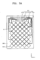
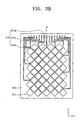
- FIGS. 3A and 3B are bottom schematic views of an encapsulation substrate and a first pattern layer formed on a surface of the encapsulation substrate in the organic light emitting display device of FIG. 1 ;
- FIG. 3C is a bottom schematic view of the first pattern layer of FIGS. 3A and 3B , and a second pattern layer on the first pattern layer;
- FIG. 3D is a cross-sectional view taken along line III-III in FIG. 3C ;
- FIG. 3E is a bottom perspective schematic view of the first pattern layer and the second pattern layer of FIG. 3C ;
- FIG. 4 is a detailed plan schematic view of the organic light emitting display device of FIG. 1 ;
- FIG. 5 is a cross-sectional view of the organic light emitting display device of FIG. 4 ;
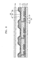
- FIG. 6 is a cross-sectional schematic view of a portion of the organic light emitting display device of FIG. 1 ;
- FIG. 7A is a bottom schematic view of an encapsulation substrate and a first pattern layer formed on a surface of the encapsulation substrate in an organic light emitting display device according to one embodiment of the present invention
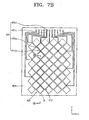
- FIG. 7B is a bottom schematic view of the first pattern layer of FIG. 7A , and a second pattern layer on the first pattern layer;
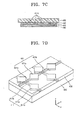
- FIG. 7C is a cross-sectional schematic view taken along line VII-VII in FIG. 7B ;
- FIG. 7D is a bottom perspective schematic view of the first pattern layer and the second pattern layer of FIG. 7B .
- FIG. 1 is a cross-sectional schematic view of a portion of an organic light emitting display device according to one embodiment of the present invention
- FIG. 2 is a plan schematic view of the organic light emitting display device of FIG. 1 .
- the encapsulation substrate 300 illustrated in FIG. 1 is not shown.
- a display unit 200 including a plurality of organic light emitting diodes (OLEDs) is formed on a substrate 100.
- the substrate 100 may be formed of transparent glass containing SiO2 as a main component, but is not limited thereto, and thus may also be formed of a transparent plastic material that may be an insulating organic material selected from the group consisting of polyethersulphone (PES), polyacrylate (PAR), polyetherimide (PEI), polyethyelene napthalate (PEN), polyethyelene terephthalate (PET), polyphenylene sulfide (PPS), polyallylate, polyimide, polycarbonate (PC), triacetate cellulose (TAC), cellulose acetate propionate (CAP), and combinations thereof.
- PES polyethersulphone
- PAR polyacrylate
- PEI polyetherimide
- PEN polyethyelene napthalate
- PET polyethyelene terephthalate
- PPS polyphenylene sulfide
- polyallylate polyimide
- PC polycarbonate
- TAC triacetate cellulose
- CAP cellulose acetate propionat
- the substrate 100 is formed of a transparent material.
- the organic light emitting display device of FIGS. 1 and 2 is a top emission type organic light-emitting display device in which an image is realized away from the substrate 100, the substrate 100 may not be necessarily formed of a transparent material, and, in this case, the substrate 100 may be formed of a metal.
- the substrate 100 may include at least one material selected from the group consisting of carbon, iron, chromium, manganese, nickel, titanium, molybdenum, stainless steel (SUS), Invar alloys, Inconel alloys, and Kovar alloys, but is not limited thereto.
- the substrate 100 may also be formed of a metal foil.
- a buffer layer may be further formed on a top surface of the substrate 100 to planarize the substrate 100 and prevent or reduce impurities from penetrating into the bottom emission type organic light emitting display device,
- the substrate 100 which includes a display unit 200 formed thereon, is attached to the encapsulation substrate 300 that is disposed above the display unit 200.
- the encapsulation substrate 300 may be formed of not only a glass material but also of various suitable plastic materials such as acryl, and furthermore, a metal.
- the encapsulation substrate 300 and touch panel related members formed on a surface of the encapsulation substrate 300 will be described later in more detail with reference to subsequent FIGS. 3A-3E .
- the substrate 100 and the encapsulation substrate 300 are attached to each other by using a sealant 250.
- the sealant 250 may be any suitable sealing glass frit.
- the sealant 250 may be formed of an organic sealant, an inorganic sealant, or of a mixture of the organic and inorganic sealants.
- the encapsulation substrate 300, and the touch panel related members formed on the surface of the encapsulation substrate 300 in the organic light emitting display device according to an embodiment of the present invention will now be described in more detail.
- a first pattern layer 310, a first insulating layer 330, a second pattern layer 320, and a second insulating layer 340 are sequentially formed on a surface of the encapsulation substrate 300, respectively, to face the substrate 100.
- An issue with a conventional organic light emitting display device having an internal electrostatic capacitive type touch panel is that the thickness of the display device is increased in order to realize a touch panel function.
- an indium tin oxide (ITO) pattern is formed on an inner surface of the encapsulation substrate 300 of the organic light emitting display device according to one embodiment of the present invention.
- the first pattern layer 310 is formed on the surface of the encapsulation substrate 300 to face the substrate 100 (see FIG. 1 ).
- the first pattern layer 310 includes a plurality of first direction pattern units 311 formed in parallel rows along a first direction (the X direction in FIG. 3A ), and a plurality of second direction pattern units 312 formed in parallel columns along a second direction (the Y direction in FIG. 3B ) that crosses (or is substantially perpendicular to) the first direction.
- the first direction pattern units 311 and the second direction pattern units 312 are alternately disposed.
- the first direction pattern units 311, each having a square shaped body rotated 45 degrees like a baseball diamond are formed in parallel rows where horizontally opposite corners of each diamond are adjacent and coupled along the first direction (the X direction in FIG. 3A ) on the surface of the encapsulation substrate 300.
- the second direction pattern units 312, each having a square shaped body rotated 45 degrees like a baseball diamond are formed in parallel columns where vertically opposite corners of each diamond are adjacent and coupled along the second direction (the Y direction in FIG. 3B ) between each of the first direction pattern units 311.
- the pattern units (311 and 312) are utilized as sensors (or sensor pads).
- Reference character A refers to one row of first direction pattern units 311 of FIG. 3A , where each row of first direction pattern units 311 includes a plurality of main bodies 311a, a plurality of connecting units 311b, an extending unit 311c, and a contact unit 311d.
- the main bodies 311a have a diamond shape, and are formed in a row along the first direction, i.e., the X direction in FIG. 3A .
- the connecting units 311b are formed between each of the main bodies 311a, and respectively connect the main bodies 311a that are adjacent to each other.
- An extending unit 311c extends from an end of each of the first direction pattern units 311.
- Each extending unit 311c is formed to extend in a direction, e.g., the Y direction in FIG. 3A , so that the plurality of extending units 311c can be arranged at one end (or end portion) of the encapsulation substrate 300, that is, an upper end of the encapsulation substrate 300 in FIG. 3A .
- a respective contact unit 311d is formed at an end (or upper end portion) of each extending unit 311c, and is electrically connected to a substrate contact unit 112 of a data line 110 (see FIG. 5 ) on the substrate 100 (see FIG. 5 ) via a conductive member 120 (see FIG. 5 ).
- reference character B refers to one column of second direction pattern units 312.
- Each column of second direction pattern units 312 includes a plurality of main bodies 312a, an extending unit 312c, and a contact unit 312d.
- the main bodies 312a have a diamond shape, and are formed in a column along the second direction, i.e., the Y direction in FIG. 3B .
- none of the second direction pattern units 312 includes a connecting unit.
- the main bodies 312a are connected to each other not by a connecting unit but by the second pattern layer 320 having a plurality of third pattern units 325 for connecting the main bodies 312a to each other (see FIG. 3E ).
- Each extending unit 312c extends from a contact unit 312d to a point in close proximity to a corner of a diamond shaped main body 312a closest to an upper end of the encapsulation substrate 300.
- the extending unit 312c is formed to extend in a direction, e.g., the Y direction in FIG. 3B , so that a plurality of extending units 312c may be arranged at one end of the encapsulation substrate 300, that is, an upper end of the encapsulation substrate 300 in FIG. 3B .
- a respective contact unit 312d is formed at an end of each extending unit 312c, and is electrically connected to a substrate contact unit of the data line 110 (see FIG. 5 ) on the substrate 100 (see FIG. 5 ) via the conductive member 120 (see FIG. 5 ).
- the first insulating layer 330 is formed on the surface of the encapsulation substrate 300 such that it faces the substrate 100 (see FIG, 1 ) and covers the first pattern layer 310.
- the first insulating layer 330 insulates the first pattern layer 310 from the second pattern layer 320.
- a plurality of contact holes (or vias) 331 may be formed at predetermined positions in the first insulating layer 330, e.g., at positions that correspond to adjacent corners of the diamond shaped main bodies 312a of the second direction pattern units 312.
- the second pattern layer 320 and the main bodies 312a of the second direction pattern units 312 are electrically connected via the contact holes 331.
- the second pattern layer 320 is formed on a surface of the first insulating layer 330 to face the substrate 100 (see FIG.1 ).
- the second pattern layer 320 a conductive layer, is formed such that it fills the contact holes 331 of the first insulating layer 330, thereby electrically connecting (e.g. by vias and third pattern units 325) the main bodies 312a of second direction pattern units 312, that are adjacent to each other.
- the first pattern layer 310 and the second pattern layer 320 may be formed of suitable transparent materials such as ITO, IZO, ZnO, and/or In2O3. Also, the first pattern layer 310 and the second pattern layer 320 may be formed by using a photolithography process. That is, an ITO layer formed by using a suitable deposition method, a spin coating method, a sputtering method, or an inkjet method may be used to form the first pattern layer 310 and the second pattern layer 320.
- a second insulating layer 340 is formed both on the surface of the first insulating layer 330 to face the substrate 100 and on the surface of the second pattern layer 320. An opposite side of the second insulating layer 340 abuts the display unit 200. The second insulating layer 340 insulates the second pattern layer 320 from a display unit 200.
- FIG. 4 is a detailed plan schematic view of the organic light emitting display device of FIG. 1
- FIG. 5 is a cross-sectional view of the organic light emitting display device of FIG. 4 .
- a contact unit 311d of a first direction pattern unit 311, and a contact unit 312d of a second direction pattern unit 312, which are formed on an encapsulation substrate 300, are electrically connected to a data line 110 formed on the substrate 100.
- the organic light emitting display device includes a conductive member 120.
- a touch panel drive IC (TDI) 113 configured to receive the electrical signals to drive and control the touch panel is disposed on the flexible PCB 130, where the electrical signals are generated by the first and second pattern layers 310 and 320 formed on the inner surface of the encapsulation substrate 300.
- the organic light emitting display device includes a conventional flexible PCB used in a display device to provide an integrated interface for enabling a touch panel function. By doing so, it is possible to effectively reduce manufacturing costs, and to improve the ease of manufacture and the user's convenience.
- the DDI 111 and the TDI 113 are shown to be separately arranged but the present invention is not limited thereto. That is, although not illustrated in the drawing, the DD1 111 may be implemented to include the functions of the TDI 113 in some embodiments. In this case, the data line 110 may be configured to be directly connected to the DDI 111. By doing so, it is possible to effectively further reduce the manufacturing costs, and to improve the manufacture and user's convenience.
- a plurality of thin film transistors 220 are formed on the substrate 100, and an organic light emitting diode (OLED) 230 is formed on (or with) each of the thin film transistors 220.
- the OLED 230 includes a pixel electrode 231 electrically connected to the thin film transistor 220, a counter electrode 235 disposed entirely on the substrate 100, and an intermediate layer 233 disposed between the pixel electrode 231 and the counter electrode 235 that includes a light emitting layer.
- the thin film transistors 220 each of which includes a gate electrode 221, source and drain electrodes 223, a semiconductor layer 227, a gate insulating layer 213, and an interlayer insulating layer 215, are formed on the substrate 100.
- the current embodiment is not limited to the thin film transistors 220 of FIG. 3D .
- other thin film transistors such as an organic thin film transistor including a semiconductor layer formed of an organic material or a silicon thin film transistor formed of silicon may also be used.
- a buffer layer 211 formed of a silicon oxide or a silicon nitride may be further included between the thin film transistors 220 and the substrate 100.
- the OLED 230 includes the pixel electrode 231 and the counter electrode 235 which effectively face each other.
- the OLED further includes the intermediate layer 233 formed of an organic material and disposed between the pixel electrode 231 and the counter electrode 235.
- the intermediate layer 233 which includes the light emitting layer, may also include a plurality of layers.
- the pixel electrode 231 may be formed as a transparent electrode or a reflective electrode. When formed as a transparent electrode, the pixel electrode 231 may be formed of ITO, IZO, ZnO, and/or In2O3. When formed as a reflective electrode, the pixel electrode 231 may include a reflection layer formed of Ag, Mg, Al, Pt, Pd, Au, Ni, Nd, Ir, Cr or combinations thereof, and a layer including ITO, IZO, ZnO, and/or In2O3, formed on the reflection layer.
- the counter electrode 235 may also be formed as a transparent electrode or a reflective electrode.
- the counter electrode 235 may include a layer in which Li, Ca, LiF/Ca, LiF/Al, Al, Mg, or combinations thereof, is deposited on the intermediate layer 233 between the pixel electrode 231 and the counter electrode 235.
- the counter electrode layer may also include a bus electrode line and an auxiliary electrode formed of ITO, IZO, ZnO, and/or In2O3.
- the counter electrode 235 may be formed by depositing Li, Ca, LiF/Ca, LiF/Al, Al, Mg or combinations thereof.
- a pixel defining layer (PDL) 219 is formed to cover an edge (or edge portion) of the pixel electrode 231 and to have a thickness (or a predetermined thickness) measured from the pixel electrode 231 to the counter electrode 235.
- the PDL 219 defines a light emitting region, and provides a wide gap between the edge of the pixel electrode 231 and the counter electrode 235 to prevent an electric field from being concentrated on the edge of the pixel electrode 231, and thereby preventing (or protecting from) a potential short circuit between the pixel electrode 231 and the counter electrode 235.
- a plurality of intermediate layers 233 each including at least a light emitting layer, may be formed between each respective pixel electrode 231 and each respective counter electrode 235.
- the intermediate layer 233 may be formed of a low molecule organic material or a polymer organic material.
- the intermediate layer 233 may have a single-layer or multiple-layer structure in which a hole injection layer (HIL), a hole transport layer (HTL), an organic light emission layer (EML), an electron transport layer (ETL), and an electron injection layer (EIL) are stacked.
- HIL hole injection layer
- HTL hole transport layer
- EML organic light emission layer
- ETL electron transport layer
- EIL electron injection layer
- the organic material include copper phthalocyanine (CuPc), N,N'-Di(naphthalene-1-yl)-N,N'-diphenyl-benzidine (NPB), tris-8-hydroxyquinoline aluminum (Alq3), etc.
- the low molecule organic material may be formed using a vacuum deposition method and a mask.
- the intermediate layer 233 may have a structure formed of an HTL and an EML;
- the HTL may be formed of poly(3,4-ethylenedioxythiophene) (PEDOT), and the EML may be formed of poly-phenylenevinylene (PPV) and polyfluorene.
- PEDOT poly(3,4-ethylenedioxythiophene)
- the EML may be formed of poly-phenylenevinylene (PPV) and polyfluorene.
- the OLED 230 is electrically connected to the thin film transistor 220 disposed there below.
- the OLED 230 is disposed on top of the planarization layer 217, and the pixel electrode 231 is electrically connected to the thin film transistor 220 via contact holes formed in the planarization layer 217.
- the OLED 230 formed on the substrate 100 is sealed by the encapsulation substrate 300.
- the encapsulation substrate 300 may be formed of various suitable materials such as glass or plastic, as described above.
- pattern layers (refer to as the first pattern layer 310 and the second pattern layer 320 in FIG. 5 ), and insulating layers (refer to as the first insulating layer 330 and the second insulating layer 340 in FIG. 5 ) are sequentially formed on the inner surface of the encapsulation substrate 300, thereby making it possible to provide a touch panel function.
- the organic light emitting display device interprets a change of an electrostatic charge (capacitance) of conductors caused by such approach, thereby sensing a touch. Based on the touch, an output is generated that includes the coordinates of the touch on the surface, and the pressing value.
- a cathode voltage flows in the counter electrode 235 (see FIG. 6 ) of the display unit 200 which contacts the second insulating layer 340.
- the first pattern layer 310 and the counter electrode 235 form one capacitor, and an electrostatic charge between the first pattern layer 310 and the counter electrode 235 is maintained constant.
- a finger, a conductive object, or a high dielectric object approaches or touches a surface above the encapsulation substrate 300, the finger and the first pattern layer 310 form a second capacitor.
- These two capacitors are effectively connected in serial, and an entire electrostatic charge changes with a touch.
- a touch sensing system can sense a touch, including the magnitude, and locate the position of the touch.
- FIG. 7A is a bottom schematic view of an encapsulation substrate 400 and a first pattern layer 410 formed on a surface of the encapsulation substrate 400 in an organic light emitting display device according to another embodiment of the present invention.
- FIG. 7B is a bottom schematic view of the first pattern layer 410 of FIG. 7A , and a second pattern layer 420 on top of the first pattern layer.
- FIG. 7C is a cross-sectional view taken along line VII-VII in FIG. 7B .
- FIG. 7D is a bottom perspective schematic view of the first pattern layer 410 and the second pattern layer 420 of FIG. 7B .
- the first pattern layer 410, a first insulating layer 430, the second pattern layer 420, and a second insulating layer 440 are sequentially formed on a surface of the encapsulation substrate 400, respectively, to face a substrate.
- the first and second direction pattern units are not formed using a single pattern layer. Instead, the first direction pattern units 411 are formed using the first pattern layer 410, while the second direction pattern units 421 are formed using the second pattern layer 420.
- the first pattern layer 410 is formed on the surface of the encapsulation substrate. 400 to face the substrate 100 (see FIG. 1 ).
- the first pattern layer 410 includes a plurality of first direction pattern units 411 formed in parallel rows along a first direction (the X direction in FIG. 7A ).
- Reference character A illustrated in FIG. 7A refers to one row of first direction pattern units 411.
- the first direction pattern units 411 are formed in parallel rows.
- the pattern units (411 and 421) are used as sensors (or sensor pads).
- Reference character A in FIG. 7A refers to one row of first direction pattern units 411, where each row of first direction pattern units 411 includes a plurality of main bodies 411a, a plurality of connecting units 411b, an extending unit 411c, and a contact unit 411d.
- the main bodies 411a have a diamond shape, and are formed in parallel rows along the first direction, i.e., the X direction in FIG. 7A .
- the connecting units 411b are formed between each of the main bodies 411a, thereby connecting the main bodies 411a which are adjacent to each other.
- the extending unit 411c extends from an end of each of the first direction pattern units 411.
- the extending unit 411c may be formed to extend in a direction, e.g., a Y direction in FIG. 7A , so that a plurality of extending units 411c may be arranged at one end of the encapsulation substrate 400, that is, an upper end of the encapsulation substrate 400 in FIG. 7A ,
- the contact unit 411d is formed at an end of the extending unit 411c, and is electrically connected to a substrate contact unit of the data line of the substrate via a conductive member,
- the first insulating layer 430 is formed on the surface of the encapsulation substrate 400 to face the substrate and to cover the first pattern layer 410.
- the first insulating layer 430 insulates the first pattern layer 410 from the second pattern layer 420.
- the second pattern layer 420 is formed on top of the first insulating layer 430 to face the substrate 100 (see FIG. 1 ).
- the second pattern layer 420 includes the second direction pattern units 421 formed in parallel columns along a second direction (the Y direction in FIG. 7B ).
- Reference character B illustrated in FIG. 7B indicates one column of second direction pattern units 421.
- the second direction pattern units 421 are formed in parallel columns.
- dashed or hidden lines indicate the first pattern layer 410 illustrated in FIG. 7A .
- reference character B refers to one column of second direction pattern units 421.
- Each column of second direction pattern units 421 includes a plurality of main bodies 421a, an extending unit 421c, and a contact unit 421d.
- the main bodies 421a have a diamond shape, and are formed in a column along the second direction, i.e., the Y direction in FIG. 7B .
- the connecting units 421b are formed between each of the main bodies 421a, thereby connecting the main bodies 421a which are adjacent to each other.
- the extending unit 421c extends from an end of each of the second direction pattern units 421.
- the extending unit 421c may be formed to extend in a direction, e.g., the Y direction in FIG.
- a plurality of extending units 421c may be arranged at one end of the encapsulation substrate 400, that is, an upper end of the encapsulation substrate 400 in FIG. 7B .
- the contact unit 421d is formed at an end of the extending unit 421c, and is electrically connected to a substrate of the data line of the substrate via the conductive member.
- the first pattern layer 410 and the second pattern layer 420 may be formed of transparent materials such as ITO, IZO, ZnO, or In2O3. Also, the first pattern layer 410 and the second pattern layer 420 may be formed by using a photolithography process. That is, an ITO layer formed by using a deposition method, a spin coating method, a sputtering method, and/or an inkjet method may be used to form the first pattern layer 410 and the second pattern layer 420.
- a second insulating layer 440 is formed on both the first insulating layer 430 to face the substrate and on the second pattern layer 420.
- An opposite side of the second insulating layer 440 faces (e.g., abuts) the display unit.
- the second insulating layer 440 insulates the second pattern layer 420 from a display unit 200 (see FIG. 5 ).
Landscapes
- Engineering & Computer Science (AREA)
- General Engineering & Computer Science (AREA)
- Theoretical Computer Science (AREA)
- Human Computer Interaction (AREA)
- Physics & Mathematics (AREA)
- General Physics & Mathematics (AREA)
- Electroluminescent Light Sources (AREA)
- Devices For Indicating Variable Information By Combining Individual Elements (AREA)
- Position Input By Displaying (AREA)
Priority Applications (1)
| Application Number | Priority Date | Filing Date | Title |
|---|---|---|---|
| EP22206982.5A EP4195007A1 (de) | 2008-07-11 | 2009-06-26 | Organische lichtemittierende und berührungsdetektierende anzeigevorrichtung |
Applications Claiming Priority (3)
| Application Number | Priority Date | Filing Date | Title |
|---|---|---|---|
| US8017908P | 2008-07-11 | 2008-07-11 | |
| US12/350,101 US8629842B2 (en) | 2008-07-11 | 2009-01-07 | Organic light emitting display device |
| EP09251664.0A EP2144146B1 (de) | 2008-07-11 | 2009-06-26 | Organische lichtemittierende und berührungsdetektierende Anzeigevorrichtung |
Related Parent Applications (2)
| Application Number | Title | Priority Date | Filing Date |
|---|---|---|---|
| EP09251664.0A Division-Into EP2144146B1 (de) | 2008-07-11 | 2009-06-26 | Organische lichtemittierende und berührungsdetektierende Anzeigevorrichtung |
| EP09251664.0 Division | 2009-06-26 |
Related Child Applications (1)
| Application Number | Title | Priority Date | Filing Date |
|---|---|---|---|
| EP22206982.5A Division EP4195007A1 (de) | 2008-07-11 | 2009-06-26 | Organische lichtemittierende und berührungsdetektierende anzeigevorrichtung |
Publications (1)
| Publication Number | Publication Date |
|---|---|
| EP2575018A1 true EP2575018A1 (de) | 2013-04-03 |
Family
ID=41226436
Family Applications (3)
| Application Number | Title | Priority Date | Filing Date |
|---|---|---|---|
| EP09251664.0A Active EP2144146B1 (de) | 2008-07-11 | 2009-06-26 | Organische lichtemittierende und berührungsdetektierende Anzeigevorrichtung |
| EP22206982.5A Pending EP4195007A1 (de) | 2008-07-11 | 2009-06-26 | Organische lichtemittierende und berührungsdetektierende anzeigevorrichtung |
| EP12197344A Ceased EP2575018A1 (de) | 2008-07-11 | 2009-06-26 | Organische lichtemittierende und berührungsdetektierende Anzeigevorrichtung |
Family Applications Before (2)
| Application Number | Title | Priority Date | Filing Date |
|---|---|---|---|
| EP09251664.0A Active EP2144146B1 (de) | 2008-07-11 | 2009-06-26 | Organische lichtemittierende und berührungsdetektierende Anzeigevorrichtung |
| EP22206982.5A Pending EP4195007A1 (de) | 2008-07-11 | 2009-06-26 | Organische lichtemittierende und berührungsdetektierende anzeigevorrichtung |
Country Status (5)
| Country | Link |
|---|---|
| US (1) | US8629842B2 (de) |
| EP (3) | EP2144146B1 (de) |
| JP (2) | JP2010020315A (de) |
| KR (1) | KR101084169B1 (de) |
| CN (2) | CN103353817A (de) |
Cited By (4)
| Publication number | Priority date | Publication date | Assignee | Title |
|---|---|---|---|---|
| US10496203B2 (en) | 2014-04-25 | 2019-12-03 | Semiconductor Energy Laboratory Co., Ltd. | Display device and electronic device |
| US10629843B2 (en) | 2014-10-17 | 2020-04-21 | Semiconductor Energy Laboratory Co., Ltd. | Light-emitting device, module, electronic device, and method for manufacturing light-emitting device |
| US10924595B2 (en) | 2013-04-15 | 2021-02-16 | Semiconductor Energy Laboratory Co., Ltd. | Light-emitting device having a bent substrate |
| US11785826B2 (en) | 2013-11-27 | 2023-10-10 | Semiconductor Energy Laboratory Co., Ltd. | Touch panel |
Families Citing this family (182)
| Publication number | Priority date | Publication date | Assignee | Title |
|---|---|---|---|---|
| US7920129B2 (en) | 2007-01-03 | 2011-04-05 | Apple Inc. | Double-sided touch-sensitive panel with shield and drive combined layer |
| US8633915B2 (en) | 2007-10-04 | 2014-01-21 | Apple Inc. | Single-layer touch-sensitive display |
| US20090174676A1 (en) | 2008-01-04 | 2009-07-09 | Apple Inc. | Motion component dominance factors for motion locking of touch sensor data |
| TWM348999U (en) * | 2008-02-18 | 2009-01-11 | Tpk Touch Solutions Inc | Capacitive touch panel |
| US8928597B2 (en) | 2008-07-11 | 2015-01-06 | Samsung Display Co., Ltd. | Organic light emitting display device |
| US9342176B2 (en) * | 2008-07-21 | 2016-05-17 | Samsung Display Co., Ltd. | Organic light emitting display device |
| JP5033078B2 (ja) * | 2008-08-06 | 2012-09-26 | 株式会社ジャパンディスプレイイースト | 表示装置 |
| US20100059294A1 (en) * | 2008-09-08 | 2010-03-11 | Apple Inc. | Bandwidth enhancement for a touch sensor panel |
| US9213450B2 (en) * | 2008-11-17 | 2015-12-15 | Tpk Touch Solutions Inc. | Touch sensor |
| JP4997607B2 (ja) * | 2008-12-12 | 2012-08-08 | Smk株式会社 | 静電容量式タッチパネル |
| US9261997B2 (en) * | 2009-02-02 | 2016-02-16 | Apple Inc. | Touch regions in diamond configuration |
| US8922521B2 (en) | 2009-02-02 | 2014-12-30 | Apple Inc. | Switching circuitry for touch sensitive display |
| US8643624B2 (en) | 2009-03-18 | 2014-02-04 | Synaptics Incorporated | Capacitive sensing using a segmented common voltage electrode of a display |
| WO2010105507A1 (zh) * | 2009-03-20 | 2010-09-23 | 宸鸿科技(厦门)有限公司 | 电容式触控电路图形及其制法 |
| WO2010117882A2 (en) * | 2009-04-10 | 2010-10-14 | Apple Inc. | Improved touch sensor panel design |
| US8593410B2 (en) | 2009-04-10 | 2013-11-26 | Apple Inc. | Touch sensor panel design |
| US8624849B2 (en) * | 2009-04-20 | 2014-01-07 | Apple Inc. | Touch actuated sensor configuration integrated with an OLED structure |
| US8587531B2 (en) * | 2009-06-10 | 2013-11-19 | Chunghwa Picture Tubes, Ltd. | Touch input device |
| US8957874B2 (en) | 2009-06-29 | 2015-02-17 | Apple Inc. | Touch sensor panel design |
| KR101058106B1 (ko) * | 2009-08-06 | 2011-08-24 | 삼성모바일디스플레이주식회사 | 표시 장치 |
| FR2949007B1 (fr) | 2009-08-07 | 2012-06-08 | Nanotec Solution | Dispositif et procede d'interface de commande sensible a un mouvement d'un corps ou d'un objet et equipement de commande integrant ce dispositif. |
| KR20110024531A (ko) * | 2009-09-02 | 2011-03-09 | 삼성모바일디스플레이주식회사 | 유기 발광 디스플레이 장치 |
| TWM380534U (en) * | 2009-11-05 | 2010-05-11 | Transtouch Technology Inc | Capacitive touch panel |
| KR101322981B1 (ko) * | 2009-12-01 | 2013-10-29 | 엘지디스플레이 주식회사 | 터치 소자를 구비한 표시장치 |
| US20110134050A1 (en) * | 2009-12-07 | 2011-06-09 | Harley Jonah A | Fabrication of touch sensor panel using laser ablation |
| KR101309862B1 (ko) * | 2009-12-10 | 2013-09-16 | 엘지디스플레이 주식회사 | 터치 패널 일체형 액정 표시 장치 |
| KR101084179B1 (ko) * | 2009-12-28 | 2011-11-17 | 삼성모바일디스플레이주식회사 | 유기 발광 디스플레이 소자의 봉지 방법 |
| US8952921B2 (en) * | 2009-12-30 | 2015-02-10 | Au Optronics Corp. | Capacitive touch display panel and capacitive touch board |
| TWI412854B (zh) * | 2010-02-04 | 2013-10-21 | Chunghwa Picture Tubes Ltd | 觸控液晶模組及其整合式觸控基板 |
| KR101093326B1 (ko) * | 2010-02-18 | 2011-12-14 | 삼성모바일디스플레이주식회사 | 터치 스크린 패널 및 그 제작방법 |
| EP2539798B1 (de) | 2010-02-26 | 2021-04-14 | Synaptics Incorporated | Demodulationsvariierung für interferenzunterdrückung |
| US20110214925A1 (en) * | 2010-03-02 | 2011-09-08 | Chao Kuo Hsieh | Touch Sensor Device |
| TWI461996B (zh) * | 2010-03-03 | 2014-11-21 | Miraenanotech Co Ltd | 靜電容式觸控面板及其製造方法 |
| TWI409684B (zh) * | 2010-03-10 | 2013-09-21 | Tpk Touch Solutions Inc | 電容式觸控結構及其製造方法 |
| TWI419022B (zh) * | 2010-03-16 | 2013-12-11 | Wintek Corp | 觸控面板結構及製作方法 |
| JP2011192567A (ja) * | 2010-03-16 | 2011-09-29 | Rohm Co Ltd | 有機el装置 |
| KR101100987B1 (ko) * | 2010-03-23 | 2011-12-30 | 삼성모바일디스플레이주식회사 | 터치 스크린 패널 |
| KR101127589B1 (ko) * | 2010-03-23 | 2012-03-26 | 삼성모바일디스플레이주식회사 | 유기 발광 디스플레이 장치 및 그 제조방법 |
| TWI540931B (zh) * | 2010-04-01 | 2016-07-01 | 友達光電股份有限公司 | 有機電激發光元件封裝及其製造方法 |
| TWI441119B (zh) | 2010-04-02 | 2014-06-11 | Arolltech Co Ltd | 具內嵌觸控裝置之顯示器 |
| CN102214048A (zh) * | 2010-04-09 | 2011-10-12 | 富晶通科技股份有限公司 | 电容式触控面板 |
| KR101048918B1 (ko) | 2010-04-28 | 2011-07-12 | 삼성모바일디스플레이주식회사 | 터치 스크린 패널 및 이를 구비한 영상표시장치 |
| KR101100949B1 (ko) | 2010-04-28 | 2011-12-29 | 삼성모바일디스플레이주식회사 | 터치 스크린 패널 및 이를 구비한 영상표시장치 |
| US9898121B2 (en) | 2010-04-30 | 2018-02-20 | Synaptics Incorporated | Integrated capacitive sensing and displaying |
| CN102236482B (zh) * | 2010-05-04 | 2013-11-06 | 宸鸿光电科技股份有限公司 | 电容式触控结构及其制造方法以及触控设备 |
| KR101056312B1 (ko) * | 2010-05-13 | 2011-08-11 | 삼성모바일디스플레이주식회사 | 터치 스크린 패널 |
| KR101756656B1 (ko) * | 2010-06-25 | 2017-07-11 | 엘지디스플레이 주식회사 | 터치 패널 내장형 유기발광다이오드 표시 장치 |
| CN102314271B (zh) * | 2010-07-07 | 2014-11-05 | 宸鸿科技(厦门)有限公司 | 一种电容式触控图形结构及其制法、触控面板及触控显示装置 |
| TWI408585B (zh) * | 2010-07-09 | 2013-09-11 | Wintek Corp | 觸控面板 |
| WO2012008759A2 (en) * | 2010-07-14 | 2012-01-19 | Lg Innotek Co., Ltd. | Touch panel and method for manufacturing the same |
| US20120019473A1 (en) * | 2010-07-21 | 2012-01-26 | Chimei Innolux Corporation | Systems for displaying images |
| US9652088B2 (en) | 2010-07-30 | 2017-05-16 | Apple Inc. | Fabrication of touch sensor panel using laser ablation |
| KR101886801B1 (ko) * | 2010-09-14 | 2018-08-10 | 삼성디스플레이 주식회사 | 터치 스크린 패널 일체형 평판표시장치 |
| KR101704536B1 (ko) | 2010-10-08 | 2017-02-09 | 삼성전자주식회사 | 슬림형 터치 패널 및 이를 포함하는 휴대 단말기 |
| KR101320109B1 (ko) * | 2010-10-26 | 2013-10-18 | 엘지디스플레이 주식회사 | 평판 표시장치용 인-셀 터치 패널 |
| KR101764415B1 (ko) | 2010-10-29 | 2017-08-16 | 삼성디스플레이 주식회사 | 터치패널 일체형 평판표시장치 |
| US8723835B2 (en) * | 2010-11-30 | 2014-05-13 | Au Optronics Corporation | Touch-sensing display panel, touch panel, touch-sensing device and touch-sensing circuit |
| KR101696483B1 (ko) * | 2010-12-06 | 2017-01-13 | 엘지디스플레이 주식회사 | 유기 발광 다이오드 표시장치 |
| CN102566837A (zh) * | 2010-12-17 | 2012-07-11 | 东莞联胜液晶显示器有限公司 | 触控显示装置 |
| US8854326B2 (en) | 2011-03-10 | 2014-10-07 | Wintek Corporation | Touch panel and touch-sensitive display device |
| CN102681712B (zh) * | 2011-03-18 | 2016-08-24 | 宸鸿科技(厦门)有限公司 | 触控装置及其制造方法 |
| CN102736760B (zh) * | 2011-04-11 | 2015-12-02 | 富创得科技股份有限公司 | 触控面板单面结构及其制作方法 |
| DE102011017383A1 (de) * | 2011-04-18 | 2012-10-18 | Ident Technology Ag | OLED-Interface |
| CN102866794A (zh) | 2011-06-15 | 2013-01-09 | 宸鸿光电科技股份有限公司 | 触控感测层及其制造方法 |
| FR2976688B1 (fr) | 2011-06-16 | 2021-04-23 | Nanotec Solution | Dispositif et procede pour generer une alimentation electrique dans un systeme electronique avec un potentiel de reference variable. |
| KR101381817B1 (ko) | 2011-06-30 | 2014-04-07 | 삼성디스플레이 주식회사 | 터치 스크린 패널 |
| CN102902425B (zh) * | 2011-07-28 | 2016-06-08 | 宸鸿科技(厦门)有限公司 | 电容式触控面板结构及制造方法 |
| CN103064551B (zh) * | 2011-10-23 | 2016-03-02 | 宸鸿科技(厦门)有限公司 | 触控感测装置及其制造方法 |
| TWI474228B (zh) * | 2011-12-02 | 2015-02-21 | Tpk Touch Solutions Inc | Touch device |
| KR101908501B1 (ko) | 2011-12-07 | 2018-10-17 | 엘지디스플레이 주식회사 | 터치 스크린 일체형 유기 발광 표시 장치 및 이의 제조 방법 |
| FR2985049B1 (fr) | 2011-12-22 | 2014-01-31 | Nanotec Solution | Dispositif de mesure capacitive a electrodes commutees pour interfaces tactiles et sans contact |
| US9262021B2 (en) * | 2012-04-11 | 2016-02-16 | Synaptics Incorporated | Two layer capacitive sensor |
| US9329723B2 (en) | 2012-04-16 | 2016-05-03 | Apple Inc. | Reconstruction of original touch image from differential touch image |
| KR101913258B1 (ko) * | 2012-05-23 | 2018-10-30 | 엘지전자 주식회사 | 터치 패널 및 이를 포함한 디스플레이 장치 |
| KR101932164B1 (ko) * | 2012-07-17 | 2019-03-21 | 삼성디스플레이 주식회사 | 터치 스크린 패널 및 이를 구비한 표시장치 |
| KR101941255B1 (ko) * | 2012-07-30 | 2019-01-23 | 삼성디스플레이 주식회사 | 터치 스크린 패널 |
| JP2015529899A (ja) * | 2012-07-31 | 2015-10-08 | インターフレックス カンパニー リミテッド | 反射防止層を含むセンサーパネル及びその製造方法 |
| WO2014021657A1 (ko) * | 2012-08-03 | 2014-02-06 | (주)인터플렉스 | 절연층이 개선된 터치패널 및 그의 제조방법 |
| KR101963810B1 (ko) * | 2012-08-22 | 2019-04-02 | 삼성디스플레이 주식회사 | 유기 발광 디스플레이 장치 |
| CN102866806A (zh) * | 2012-09-25 | 2013-01-09 | 大连七色光太阳能科技开发有限公司 | 一种fto导电玻璃用于二屏合一触摸屏的生产方法 |
| CN102929465B (zh) * | 2012-11-12 | 2016-02-24 | 汕头超声显示器(二厂)有限公司 | 一种电容触控显示组件及其制造方法 |
| TWI476659B (zh) * | 2012-12-20 | 2015-03-11 | Henghao Technology Co Ltd | 雙層電極裝置 |
| KR102074418B1 (ko) * | 2013-01-29 | 2020-02-07 | 삼성디스플레이 주식회사 | 플렉서블 터치 스크린 패널 |
| US9336723B2 (en) * | 2013-02-13 | 2016-05-10 | Apple Inc. | In-cell touch for LED |
| CN103279248B (zh) * | 2013-06-06 | 2017-03-01 | 敦泰科技有限公司 | 集成触控有机发光二极管显示装置 |
| KR20150008711A (ko) * | 2013-07-15 | 2015-01-23 | 삼성디스플레이 주식회사 | 접촉 감지 기능이 있는 유기 발광 표시 장치 및 그 제조 방법 |
| US9886141B2 (en) | 2013-08-16 | 2018-02-06 | Apple Inc. | Mutual and self capacitance touch measurements in touch panel |
| JP6253923B2 (ja) * | 2013-08-30 | 2017-12-27 | 株式会社ジャパンディスプレイ | タッチセンサ内蔵有機エレクトロルミネッセンス装置 |
| KR102091035B1 (ko) * | 2013-09-03 | 2020-03-20 | 엘지디스플레이 주식회사 | 터치 스크린을 가지는 표시장치 |
| KR102159189B1 (ko) | 2013-11-05 | 2020-09-24 | 삼성디스플레이 주식회사 | 표시 장치, 터치 패널 장치, 터치 패널 구동 ic 장치 및 터치 패널 구동 방법 |
| KR102135360B1 (ko) | 2013-11-18 | 2020-07-17 | 엘지전자 주식회사 | 반도체 발광 소자를 이용한 디스플레이 장치 |
| KR102192035B1 (ko) | 2013-12-02 | 2020-12-17 | 삼성디스플레이 주식회사 | 접촉 감지 센서를 포함하는 플렉서블 표시 장치 |
| KR101984443B1 (ko) | 2013-12-13 | 2019-05-30 | 애플 인크. | 자기-정전용량성 터치 센서를 위한 통합된 터치 및 디스플레이 아키텍처 |
| CN104750321B (zh) * | 2013-12-26 | 2018-09-04 | 昆山国显光电有限公司 | 一种触控显示装置及其制备方法 |
| CN104750284B (zh) * | 2013-12-27 | 2019-02-19 | 昆山工研院新型平板显示技术中心有限公司 | 一种触控显示装置及其制备方法 |
| CN104750285B (zh) * | 2013-12-27 | 2019-01-18 | 昆山工研院新型平板显示技术中心有限公司 | 一种触控显示装置及其制备方法 |
| KR102168132B1 (ko) * | 2013-12-31 | 2020-10-21 | 삼성디스플레이 주식회사 | 유기 발광 표시 장치 |
| CN103744557B (zh) * | 2014-01-15 | 2016-10-12 | 昆山龙腾光电有限公司 | 触控显示装置 |
| DE102014100803B4 (de) | 2014-01-24 | 2022-03-31 | Preh Gmbh | Verfahren zur Herstellung einer Elektrodenanordnung für ein berührungsempfindliches kapazitives Eingabegerät sowie Elektrodenanordnung und Eingabegerät |
| KR102181237B1 (ko) * | 2014-03-17 | 2020-11-23 | 삼성디스플레이 주식회사 | 디스플레이 장치 |
| JP2015195010A (ja) * | 2014-03-20 | 2015-11-05 | パナソニックIpマネジメント株式会社 | タッチセンサ機能を有する入力装置および表示装置 |
| KR20150114632A (ko) * | 2014-04-01 | 2015-10-13 | 삼성디스플레이 주식회사 | 터치 유닛 및 이를 포함하는 터치 표시 장치 |
| US10411078B2 (en) | 2014-04-14 | 2019-09-10 | Industrial Technology Research Institute | Sensing display apparatus |
| TWI613580B (zh) * | 2017-01-25 | 2018-02-01 | 財團法人工業技術研究院 | 感測顯示裝置 |
| TWM505004U (zh) | 2014-04-14 | 2015-07-11 | Ind Tech Res Inst | 觸控面板 |
| US20150324047A1 (en) * | 2014-05-07 | 2015-11-12 | Lg Innotek Co., Ltd. | Touch panel including patterns of mesh structures |
| KR102261949B1 (ko) * | 2014-05-07 | 2021-06-08 | 엘지이노텍 주식회사 | 메시 구조의 패턴을 구비한 터치 패널 |
| KR102237859B1 (ko) * | 2014-05-14 | 2021-04-09 | 엘지이노텍 주식회사 | 터치 패널 및 이를 포함하는 터치 디바이스 |
| US10133382B2 (en) | 2014-05-16 | 2018-11-20 | Apple Inc. | Structure for integrated touch screen |
| WO2015178920A1 (en) | 2014-05-22 | 2015-11-26 | Onamp Research Llc | Panel bootstrapping architectures for in-cell self-capacitance |
| CN103984442B (zh) * | 2014-05-27 | 2017-10-31 | 上海和辉光电有限公司 | 内嵌式有源矩阵有机发光二极管触控面板 |
| US10289251B2 (en) | 2014-06-27 | 2019-05-14 | Apple Inc. | Reducing floating ground effects in pixelated self-capacitance touch screens |
| TW201602879A (zh) * | 2014-07-04 | 2016-01-16 | 勝華科技股份有限公司 | 觸控面板 |
| CN104216562B (zh) * | 2014-08-22 | 2017-06-30 | 京东方科技集团股份有限公司 | 触控面板及其制造方法和显示装置 |
| US9880655B2 (en) | 2014-09-02 | 2018-01-30 | Apple Inc. | Method of disambiguating water from a finger touch on a touch sensor panel |
| CN107077260B (zh) | 2014-09-22 | 2020-05-12 | 苹果公司 | 触摸控制器和用于触摸传感器面板的方法 |
| KR102260263B1 (ko) * | 2014-10-14 | 2021-06-02 | 엘지디스플레이 주식회사 | 터치 패널 및 터치 패널 일체형 유기 발광 표시 장치 |
| US10712867B2 (en) | 2014-10-27 | 2020-07-14 | Apple Inc. | Pixelated self-capacitance water rejection |
| CN104409469B (zh) * | 2014-10-30 | 2017-02-15 | 京东方科技集团股份有限公司 | 一种amoled触控显示装置及其制备方法、驱动方法 |
| WO2016072983A1 (en) | 2014-11-05 | 2016-05-12 | Onamp Research Llc | Common electrode driving and compensation for pixelated self-capacitance touch screen |
| CN104317470B (zh) * | 2014-11-14 | 2017-06-13 | 深圳市华星光电技术有限公司 | 互电容式ogs触摸面板及其制造方法 |
| KR102289934B1 (ko) * | 2014-11-28 | 2021-08-13 | 삼성디스플레이 주식회사 | 터치 감지 센서를 포함하는 표시 장치 |
| CN104503609A (zh) * | 2014-12-04 | 2015-04-08 | 深圳市华星光电技术有限公司 | Oled触控显示装置及其制造方法 |
| CN104461152A (zh) * | 2014-12-23 | 2015-03-25 | 昆山国显光电有限公司 | 触控显示面板及触控显示装置 |
| KR20160090449A (ko) | 2015-01-21 | 2016-08-01 | 삼성디스플레이 주식회사 | 표시 장치 및 그 제조 방법 |
| AU2016215616B2 (en) | 2015-02-02 | 2018-12-06 | Apple Inc. | Flexible self-capacitance and mutual capacitance touch sensing system architecture |
| KR101641265B1 (ko) * | 2015-02-04 | 2016-07-20 | 엘지전자 주식회사 | 반도체 발광 소자를 이용한 디스플레이 장치 |
| KR102350029B1 (ko) * | 2015-02-17 | 2022-01-11 | 삼성디스플레이 주식회사 | 신축성 표시 장치 및 이의 제조 방법 |
| US10488992B2 (en) | 2015-03-10 | 2019-11-26 | Apple Inc. | Multi-chip touch architecture for scalability |
| CN104733502B (zh) * | 2015-03-13 | 2018-03-30 | 上海和辉光电有限公司 | Amoled面板及其制作方法 |
| JP2016178071A (ja) * | 2015-03-18 | 2016-10-06 | 芳廣 菊地 | 静電容量式タッチスイッチ電極 |
| US10146359B2 (en) | 2015-04-28 | 2018-12-04 | Apple Inc. | Common electrode auto-compensation method |
| CN105159485B (zh) * | 2015-06-18 | 2018-06-05 | 京东方科技集团股份有限公司 | 触控面板及其制备方法、显示装置 |
| EP3316307A4 (de) * | 2015-06-25 | 2019-02-20 | Shenzhen Royole Technologies Co., Ltd. | Verfahren zur herstellung einer berührungsbildschirmanzeige |
| CN104991683B (zh) * | 2015-07-22 | 2019-02-12 | 京东方科技集团股份有限公司 | 一种oled触控显示面板及其控制方法、显示装置 |
| US10386962B1 (en) | 2015-08-03 | 2019-08-20 | Apple Inc. | Reducing touch node electrode coupling |
| US10365773B2 (en) | 2015-09-30 | 2019-07-30 | Apple Inc. | Flexible scan plan using coarse mutual capacitance and fully-guarded measurements |
| KR102460509B1 (ko) | 2015-10-06 | 2022-10-31 | 삼성디스플레이 주식회사 | 유기 발광 표시 장치 및 유기 발광 표시 장치의 제조 방법 |
| CN105655378A (zh) * | 2016-01-04 | 2016-06-08 | 京东方科技集团股份有限公司 | 一种阵列基板和oled显示面板、制备方法及显示装置 |
| KR102562627B1 (ko) | 2016-03-21 | 2023-08-03 | 삼성디스플레이 주식회사 | 디스플레이 장치 |
| KR102556838B1 (ko) | 2016-06-01 | 2023-07-19 | 삼성디스플레이 주식회사 | 터치 패널, 이를 포함하는 전자 장치, 및 터치 패널 제조 방법 |
| CN105914214B (zh) * | 2016-06-15 | 2019-06-14 | 深圳市飞鸣特科技有限公司 | Oled显示面板制造方法及薄膜晶体管阵列基板制造方法 |
| KR101931768B1 (ko) * | 2016-06-30 | 2018-12-24 | 삼성디스플레이 주식회사 | 전자 장치 |
| KR101913394B1 (ko) | 2016-07-29 | 2018-10-31 | 삼성디스플레이 주식회사 | 표시 장치 |
| CN109564485B (zh) | 2016-07-29 | 2022-04-01 | 苹果公司 | 具有多电源域芯片配置的触摸传感器面板 |
| KR102387795B1 (ko) * | 2016-08-31 | 2022-04-15 | 엘지디스플레이 주식회사 | 터치 센서를 가지는 유기 발광 표시 장치 |
| CN106206668B (zh) * | 2016-08-31 | 2019-04-05 | 昆山国显光电有限公司 | 一种有源矩阵有机发光二极管显示装置以及制作方法 |
| AU2017208277B2 (en) | 2016-09-06 | 2018-12-20 | Apple Inc. | Back of cover touch sensors |
| KR102564349B1 (ko) * | 2016-09-30 | 2023-08-04 | 엘지디스플레이 주식회사 | 유기 발광 표시 장치 |
| KR102659604B1 (ko) | 2016-11-04 | 2024-04-23 | 삼성디스플레이 주식회사 | 터치 센서 및 이를 포함하는 표시 장치 |
| CN108121939A (zh) * | 2016-11-28 | 2018-06-05 | 南昌欧菲生物识别技术有限公司 | 有机发光二极管显示屏指纹识别装置及电子设备 |
| US10181574B2 (en) * | 2016-12-29 | 2019-01-15 | Lg Display Co., Ltd. | Organic light emitting device |
| JP6546943B2 (ja) * | 2017-02-13 | 2019-07-17 | 株式会社ジャパンディスプレイ | タッチパネル機能内蔵表示装置 |
| JP6901888B2 (ja) * | 2017-03-27 | 2021-07-14 | 株式会社ジャパンディスプレイ | タッチセンサ内蔵表示装置 |
| WO2018188075A1 (en) * | 2017-04-14 | 2018-10-18 | Boe Technology Group Co., Ltd. | Touch substrate, touch control display panel, and touch control display apparatus |
| US10642418B2 (en) | 2017-04-20 | 2020-05-05 | Apple Inc. | Finger tracking in wet environment |
| CN110870384B (zh) * | 2017-07-13 | 2022-07-05 | 堺显示器制品株式会社 | 有机el设备及其制造方法 |
| KR102281226B1 (ko) * | 2017-07-18 | 2021-07-22 | 엘지디스플레이 주식회사 | 표시장치 |
| KR102380755B1 (ko) * | 2017-10-25 | 2022-03-30 | 엘지디스플레이 주식회사 | 터치 디스플레이 패널 및 터치 디스플레이 장치 |
| KR102467371B1 (ko) * | 2017-11-09 | 2022-11-14 | 엘지디스플레이 주식회사 | 전계발광 표시장치 및 그 제조방법 |
| KR102419066B1 (ko) | 2017-11-20 | 2022-07-08 | 엘지디스플레이 주식회사 | 터치 디스플레이 패널 및 터치 디스플레이 장치 |
| CN108447889B (zh) * | 2018-03-29 | 2021-01-26 | 京东方科技集团股份有限公司 | 触控面板、其制备方法和触控显示装置 |
| KR102570978B1 (ko) * | 2018-04-18 | 2023-08-25 | 엘지디스플레이 주식회사 | 터치 센서를 가지는 유기 발광 표시 장치 |
| KR102019774B1 (ko) * | 2018-08-02 | 2019-11-05 | 삼성디스플레이 주식회사 | 표시장치 |
| KR102846212B1 (ko) * | 2018-09-21 | 2025-08-14 | 삼성디스플레이 주식회사 | 표시 장치 |
| CN109815918B (zh) * | 2019-01-28 | 2021-11-05 | 京东方科技集团股份有限公司 | 指纹识别模组及其制作方法和驱动方法、显示装置 |
| KR102092709B1 (ko) * | 2019-03-25 | 2020-03-25 | 삼성디스플레이 주식회사 | 유기 발광 디스플레이 장치 |
| KR102085060B1 (ko) * | 2019-09-03 | 2020-03-06 | 삼성디스플레이 주식회사 | 표시장치 |
| KR102322819B1 (ko) * | 2019-09-03 | 2021-11-09 | 삼성디스플레이 주식회사 | 표시장치 |
| US11157109B1 (en) | 2019-09-06 | 2021-10-26 | Apple Inc. | Touch sensing with water rejection |
| KR102774516B1 (ko) | 2020-03-20 | 2025-03-05 | 삼성디스플레이 주식회사 | 표시 장치 |
| CN111427474A (zh) * | 2020-03-20 | 2020-07-17 | 深圳市华星光电半导体显示技术有限公司 | 触控显示装置及触控显示装置制作方法 |
| US11662867B1 (en) | 2020-05-30 | 2023-05-30 | Apple Inc. | Hover detection on a touch sensor panel |
| KR102826935B1 (ko) | 2020-11-13 | 2025-07-01 | 삼성디스플레이 주식회사 | 표시장치 |
| US12193283B2 (en) | 2020-11-19 | 2025-01-07 | Samsung Display Co., Ltd. | Display device including pad area |
| KR102839630B1 (ko) * | 2020-12-30 | 2025-07-28 | 엘지디스플레이 주식회사 | 표시 장치 |
| KR102385336B1 (ko) * | 2021-04-09 | 2022-04-11 | 삼성디스플레이 주식회사 | 표시 장치 |
| KR20220155541A (ko) | 2021-05-14 | 2022-11-23 | 삼성디스플레이 주식회사 | 표시장치 |
| KR20230013666A (ko) | 2021-07-15 | 2023-01-27 | 삼성디스플레이 주식회사 | 표시 장치 |
| KR20230055471A (ko) | 2021-10-18 | 2023-04-26 | 삼성디스플레이 주식회사 | 디스플레이 장치 |
| CN113805736B (zh) * | 2021-10-27 | 2025-06-17 | 紫光计算机科技有限公司 | 一种触控显示板及其制备方法 |
| US12198627B2 (en) | 2022-08-23 | 2025-01-14 | Samsung Display Co., Ltd. | Display apparatus |
Citations (4)
| Publication number | Priority date | Publication date | Assignee | Title |
|---|---|---|---|---|
| DE10308514A1 (de) * | 2003-02-26 | 2004-09-09 | Schott Glas | OLED mit Berührungssensor |
| US20070240914A1 (en) * | 2006-04-14 | 2007-10-18 | Ritdisplay Corporation | Transparent touch panel |
| WO2008002043A1 (en) * | 2006-06-30 | 2008-01-03 | Youngjong Lee | Method and system for providing touch sensing function to organic light emitting diode |
| US20080165158A1 (en) * | 2007-01-05 | 2008-07-10 | Apple Inc. | Touch screen stack-ups |
Family Cites Families (69)
| Publication number | Priority date | Publication date | Assignee | Title |
|---|---|---|---|---|
| JPH03134925A (ja) | 1989-10-20 | 1991-06-07 | Toshiba Corp | ガス絶縁断路器 |
| JP2653014B2 (ja) | 1993-07-26 | 1997-09-10 | 日本電気株式会社 | アクティブマトリックス液晶ディスプレイ装置 |
| JPH1091342A (ja) * | 1996-09-12 | 1998-04-10 | Sanyo Electric Co Ltd | 携帯用情報端末 |
| JP3134925B2 (ja) | 1997-04-04 | 2001-02-13 | サンケン電気株式会社 | 回路基板等の板状体の固着方法及び装置 |
| US7663607B2 (en) * | 2004-05-06 | 2010-02-16 | Apple Inc. | Multipoint touchscreen |
| US6512512B1 (en) | 1999-07-31 | 2003-01-28 | Litton Systems, Inc. | Touch panel with improved optical performance |
| JP2001076886A (ja) * | 1999-09-03 | 2001-03-23 | Futaba Corp | 透明タッチスイッチ付き有機elデバイスとその製造方法 |
| US6664950B1 (en) | 1999-11-17 | 2003-12-16 | L-3 Communications | Resistive touch panel using removable, tensioned top layer |
| JP3384397B2 (ja) | 2000-05-25 | 2003-03-10 | セイコーエプソン株式会社 | 液晶装置、その製造方法および電子機器 |
| US6980184B1 (en) * | 2000-09-27 | 2005-12-27 | Alien Technology Corporation | Display devices and integrated circuits |
| JP4092914B2 (ja) | 2001-01-26 | 2008-05-28 | セイコーエプソン株式会社 | マスクの製造方法、有機エレクトロルミネッセンス装置の製造方法 |
| GB2371910A (en) * | 2001-01-31 | 2002-08-07 | Seiko Epson Corp | Display devices |
| KR20030028973A (ko) | 2001-10-05 | 2003-04-11 | 비오이 하이디스 테크놀로지 주식회사 | 터치형 액정표시장치 |
| JP4507480B2 (ja) | 2001-12-27 | 2010-07-21 | ソニー株式会社 | 表示装置 |
| AU2003209595A1 (en) | 2002-03-20 | 2003-09-29 | Koninklijke Philips Electronics N.V. | Active matrix electroluminescent display devices, and their manufacture |
| US7184009B2 (en) * | 2002-06-21 | 2007-02-27 | Nokia Corporation | Display circuit with optical sensor |
| JP4010008B2 (ja) * | 2002-10-01 | 2007-11-21 | ソニー株式会社 | 有機発光表示装置およびその製造方法 |
| US7936338B2 (en) * | 2002-10-01 | 2011-05-03 | Sony Corporation | Display unit and its manufacturing method |
| US6879319B2 (en) * | 2002-10-25 | 2005-04-12 | Eastman Kodak Company | Integrated OLED display and touch screen |
| KR100497095B1 (ko) * | 2002-12-26 | 2005-06-28 | 엘지.필립스 엘시디 주식회사 | 듀얼패널타입 유기전계발광 소자용 어레이 기판 및 그 제조방법 |
| JP2004265776A (ja) * | 2003-03-03 | 2004-09-24 | Hitachi Ltd | 有機elディスプレイ装置 |
| TWI307425B (en) | 2003-05-16 | 2009-03-11 | Sharp Kk | Liquid crystal display device |
| JP4220305B2 (ja) * | 2003-05-22 | 2009-02-04 | 三星エスディアイ株式会社 | 有機エレクトロルミネセンス素子 |
| US20050030048A1 (en) * | 2003-08-05 | 2005-02-10 | Bolender Robert J. | Capacitive sensing device for use in a keypad assembly |
| JP2005107890A (ja) * | 2003-09-30 | 2005-04-21 | Sanyo Electric Co Ltd | El表示装置 |
| US20050248270A1 (en) * | 2004-05-05 | 2005-11-10 | Eastman Kodak Company | Encapsulating OLED devices |
| JP2006004907A (ja) * | 2004-05-18 | 2006-01-05 | Seiko Epson Corp | エレクトロルミネッセンス装置及び電子機器 |
| JP2005339406A (ja) | 2004-05-28 | 2005-12-08 | Sanyo Electric Co Ltd | タッチパネル |
| KR100600883B1 (ko) | 2004-11-11 | 2006-07-18 | 삼성에스디아이 주식회사 | 유기 전계 발광 소자 및 그 제조 방법 |
| KR20060056634A (ko) * | 2004-11-22 | 2006-05-25 | 삼성전자주식회사 | 광센서를 내장하는 표시 장치 및 감지 신호 처리 방법 |
| US7671833B2 (en) * | 2004-11-22 | 2010-03-02 | Samsung Electronics Co., Ltd. | Touch sensible display device |
| WO2006068782A2 (en) * | 2004-12-22 | 2006-06-29 | 3M Innovative Properties Company | Touch sensors incorporating capacitively coupled electrodes |
| JP4942341B2 (ja) | 2004-12-24 | 2012-05-30 | 三洋電機株式会社 | 表示装置 |
| TWI267014B (en) * | 2005-02-21 | 2006-11-21 | Au Optronics Corp | Organic light emitting diode display |
| KR100612240B1 (ko) | 2005-03-04 | 2006-08-11 | 삼성에스디아이 주식회사 | 플라즈마 디스플레이 패널 |
| TWI271645B (en) | 2005-04-19 | 2007-01-21 | Elan Microelectronics Corp | Capacitive touchpad with a physical key function |
| US7439962B2 (en) * | 2005-06-01 | 2008-10-21 | Synaptics Incorporated | Touch pad with flexible substrate |
| KR100721948B1 (ko) | 2005-08-30 | 2007-05-25 | 삼성에스디아이 주식회사 | 유기 전계 발광 표시 장치 및 그의 제조 방법 |
| US7932898B2 (en) | 2005-09-20 | 2011-04-26 | Atmel Corporation | Touch sensitive screen |
| GB0519170D0 (en) | 2005-09-20 | 2005-10-26 | Philipp Harald | Capacitive touch sensor |
| US8144115B2 (en) * | 2006-03-17 | 2012-03-27 | Konicek Jeffrey C | Flat panel display screen operable for touch position determination system and methods |
| TWI317086B (en) * | 2006-04-14 | 2009-11-11 | Ritdisplay Corp | Top-emitting organic led display having transparent touch panel |
| JP4838643B2 (ja) | 2006-06-27 | 2011-12-14 | オプトレックス株式会社 | 入力装置付表示装置 |
| US8040321B2 (en) | 2006-07-10 | 2011-10-18 | Cypress Semiconductor Corporation | Touch-sensor with shared capacitive sensors |
| CN101512469B (zh) | 2006-09-11 | 2011-11-30 | 夏普株式会社 | 包括触控面板的显示装置 |
| KR100829750B1 (ko) | 2006-12-06 | 2008-05-15 | 삼성에스디아이 주식회사 | 유기 발광 표시 장치 |
| JP4910780B2 (ja) * | 2007-03-02 | 2012-04-04 | セイコーエプソン株式会社 | 入力機能付有機エレクトロルミネッセンス装置、及び電子機器 |
| JP5103944B2 (ja) | 2007-03-02 | 2012-12-19 | セイコーエプソン株式会社 | 入力機能付有機エレクトロルミネッセンス装置、及び電子機器 |
| US7715085B2 (en) | 2007-05-09 | 2010-05-11 | Qualcomm Mems Technologies, Inc. | Electromechanical system having a dielectric movable membrane and a mirror |
| US7643202B2 (en) | 2007-05-09 | 2010-01-05 | Qualcomm Mems Technologies, Inc. | Microelectromechanical system having a dielectric movable membrane and a mirror |
| KR100873080B1 (ko) * | 2007-05-10 | 2008-12-09 | 삼성모바일디스플레이주식회사 | 유기 전계 발광표시장치 |
| TW200844827A (en) | 2007-05-11 | 2008-11-16 | Sense Pad Tech Co Ltd | Transparent touch panel device |
| US20080309633A1 (en) | 2007-06-13 | 2008-12-18 | Apple Inc. | Touch-sensitive display |
| JP4998919B2 (ja) | 2007-06-14 | 2012-08-15 | ソニーモバイルディスプレイ株式会社 | 静電容量型入力装置 |
| JP4506785B2 (ja) | 2007-06-14 | 2010-07-21 | エプソンイメージングデバイス株式会社 | 静電容量型入力装置 |
| JP4924314B2 (ja) | 2007-09-14 | 2012-04-25 | セイコーエプソン株式会社 | 有機el装置および電子機器 |
| KR20090058072A (ko) | 2007-12-04 | 2009-06-09 | 주식회사 협진아이엔씨 | 원 레이어 방식 정전용량 터치스크린 및 그 제조방법 |
| JP5366037B2 (ja) | 2007-12-21 | 2013-12-11 | 株式会社ジャパンディスプレイ | 電気光学装置及び電子機器 |
| JP4945483B2 (ja) | 2008-02-27 | 2012-06-06 | 株式会社 日立ディスプレイズ | 表示パネル |
| JP2009251592A (ja) * | 2008-04-03 | 2009-10-29 | Samsung Mobile Display Co Ltd | 有機電界発光表示装置 |
| KR100987381B1 (ko) * | 2008-07-16 | 2010-10-12 | 삼성모바일디스플레이주식회사 | 유기 발광 디스플레이 장치 |
| US8928597B2 (en) | 2008-07-11 | 2015-01-06 | Samsung Display Co., Ltd. | Organic light emitting display device |
| US9342176B2 (en) | 2008-07-21 | 2016-05-17 | Samsung Display Co., Ltd. | Organic light emitting display device |
| WO2010032329A1 (ja) * | 2008-09-22 | 2010-03-25 | パイオニア株式会社 | El発光装置 |
| TWI380089B (en) | 2008-12-03 | 2012-12-21 | Au Optronics Corp | Method of forming a color filter touch sensing substrate |
| US20100214247A1 (en) | 2009-02-20 | 2010-08-26 | Acrosense Technology Co., Ltd. | Capacitive Touch Panel |
| TWI398799B (zh) | 2009-06-18 | 2013-06-11 | Ritfast Corp | 觸控面板 |
| KR101058106B1 (ko) | 2009-08-06 | 2011-08-24 | 삼성모바일디스플레이주식회사 | 표시 장치 |
| KR101082293B1 (ko) | 2009-09-04 | 2011-11-09 | 삼성모바일디스플레이주식회사 | 터치 스크린 패널 |
-
2009
- 2009-01-07 US US12/350,101 patent/US8629842B2/en active Active
- 2009-05-14 CN CN2013102472110A patent/CN103353817A/zh active Pending
- 2009-05-14 CN CN200910138692.5A patent/CN101626017B/zh active Active
- 2009-06-16 KR KR1020090053490A patent/KR101084169B1/ko active Active
- 2009-06-26 EP EP09251664.0A patent/EP2144146B1/de active Active
- 2009-06-26 EP EP22206982.5A patent/EP4195007A1/de active Pending
- 2009-06-26 EP EP12197344A patent/EP2575018A1/de not_active Ceased
- 2009-07-10 JP JP2009163881A patent/JP2010020315A/ja active Pending
-
2012
- 2012-03-29 JP JP2012076237A patent/JP5508461B2/ja active Active
Patent Citations (4)
| Publication number | Priority date | Publication date | Assignee | Title |
|---|---|---|---|---|
| DE10308514A1 (de) * | 2003-02-26 | 2004-09-09 | Schott Glas | OLED mit Berührungssensor |
| US20070240914A1 (en) * | 2006-04-14 | 2007-10-18 | Ritdisplay Corporation | Transparent touch panel |
| WO2008002043A1 (en) * | 2006-06-30 | 2008-01-03 | Youngjong Lee | Method and system for providing touch sensing function to organic light emitting diode |
| US20080165158A1 (en) * | 2007-01-05 | 2008-07-10 | Apple Inc. | Touch screen stack-ups |
Cited By (12)
| Publication number | Priority date | Publication date | Assignee | Title |
|---|---|---|---|---|
| US10924595B2 (en) | 2013-04-15 | 2021-02-16 | Semiconductor Energy Laboratory Co., Ltd. | Light-emitting device having a bent substrate |
| US11095763B2 (en) | 2013-04-15 | 2021-08-17 | Semiconductor Energy Laboratory Co., Ltd. | Light-emitting device having multiple curved regions |
| US11723253B2 (en) | 2013-04-15 | 2023-08-08 | Semiconductor Energy Laboratory Co., Ltd. | Light-emitting device including flexible printed circuit |
| US12156455B2 (en) | 2013-04-15 | 2024-11-26 | Semiconductor Energy Laboratory Co., Ltd. | Light-emitting device including curved regions |
| US11785826B2 (en) | 2013-11-27 | 2023-10-10 | Semiconductor Energy Laboratory Co., Ltd. | Touch panel |
| US12336415B2 (en) | 2013-11-27 | 2025-06-17 | Semiconductor Energy Laboratory Co., Ltd. | Touch panel |
| US10496203B2 (en) | 2014-04-25 | 2019-12-03 | Semiconductor Energy Laboratory Co., Ltd. | Display device and electronic device |
| US11199920B2 (en) | 2014-04-25 | 2021-12-14 | Semiconductor Energy Laboratory Co., Ltd. | Display device and electronic device |
| US11669181B2 (en) | 2014-04-25 | 2023-06-06 | Semiconductor Energy Laboratory Co., Ltd. | Display device and electronic device |
| US10629843B2 (en) | 2014-10-17 | 2020-04-21 | Semiconductor Energy Laboratory Co., Ltd. | Light-emitting device, module, electronic device, and method for manufacturing light-emitting device |
| US11189817B2 (en) | 2014-10-17 | 2021-11-30 | Semiconductor Energy Laboratory Co., Ltd. | Light-emitting device, module, electronic device, and method for manufacturing light-emitting device |
| US11778850B2 (en) | 2014-10-17 | 2023-10-03 | Semiconductor Energy Laboratory Co., Ltd. | Light-emitting device, module, electronic device, and method for manufacturing light-emitting device |
Also Published As
| Publication number | Publication date |
|---|---|
| JP2010020315A (ja) | 2010-01-28 |
| JP2012156140A (ja) | 2012-08-16 |
| CN101626017A (zh) | 2010-01-13 |
| US20100007616A1 (en) | 2010-01-14 |
| EP4195007A1 (de) | 2023-06-14 |
| US8629842B2 (en) | 2014-01-14 |
| CN101626017B (zh) | 2014-08-20 |
| KR101084169B1 (ko) | 2011-11-17 |
| EP2144146B1 (de) | 2019-08-14 |
| EP2144146A1 (de) | 2010-01-13 |
| CN103353817A (zh) | 2013-10-16 |
| KR20100007717A (ko) | 2010-01-22 |
| JP5508461B2 (ja) | 2014-05-28 |
Similar Documents
| Publication | Publication Date | Title |
|---|---|---|
| US10936132B2 (en) | Organic light emitting display device | |
| EP2144146B1 (de) | Organische lichtemittierende und berührungsdetektierende Anzeigevorrichtung | |
| KR101050464B1 (ko) | 디스플레이 패널 및 그 제조 방법 | |
| KR101127589B1 (ko) | 유기 발광 디스플레이 장치 및 그 제조방법 | |
| US8743078B2 (en) | Display apparatus | |
| US9483135B2 (en) | Organic light emitting display integrated with touch screen panel | |
| US8681107B2 (en) | Organic light emitting display apparatus and method of manufacturing the same | |
| US20150130726A1 (en) | Organic light-emitting diode (oled) display |
Legal Events
| Date | Code | Title | Description |
|---|---|---|---|
| PUAI | Public reference made under article 153(3) epc to a published international application that has entered the european phase |
Free format text: ORIGINAL CODE: 0009012 |
|
| 17P | Request for examination filed |
Effective date: 20121214 |
|
| AC | Divisional application: reference to earlier application |
Ref document number: 2144146 Country of ref document: EP Kind code of ref document: P |
|
| AK | Designated contracting states |
Kind code of ref document: A1 Designated state(s): AT BE BG CH CY CZ DE DK EE ES FI FR GB GR HR HU IE IS IT LI LT LU LV MC MK MT NL NO PL PT RO SE SI SK TR |
|
| 17Q | First examination report despatched |
Effective date: 20150821 |
|
| RAP1 | Party data changed (applicant data changed or rights of an application transferred) |
Owner name: SAMSUNG DISPLAY CO., LTD. |
|
| STAA | Information on the status of an ep patent application or granted ep patent |
Free format text: STATUS: EXAMINATION IS IN PROGRESS |
|
| APBK | Appeal reference recorded |
Free format text: ORIGINAL CODE: EPIDOSNREFNE |
|
| APBN | Date of receipt of notice of appeal recorded |
Free format text: ORIGINAL CODE: EPIDOSNNOA2E |
|
| APBR | Date of receipt of statement of grounds of appeal recorded |
Free format text: ORIGINAL CODE: EPIDOSNNOA3E |
|
| APAF | Appeal reference modified |
Free format text: ORIGINAL CODE: EPIDOSCREFNE |
|
| APBT | Appeal procedure closed |
Free format text: ORIGINAL CODE: EPIDOSNNOA9E |
|
| STAA | Information on the status of an ep patent application or granted ep patent |
Free format text: STATUS: THE APPLICATION HAS BEEN REFUSED |
|
| 18R | Application refused |
Effective date: 20221114 |