EP2500929A1 - Schlamm für chemisch-mechanisches polieren und verfahren zum polieren von substraten damit - Google Patents
Schlamm für chemisch-mechanisches polieren und verfahren zum polieren von substraten damit Download PDFInfo
- Publication number
- EP2500929A1 EP2500929A1 EP10829911A EP10829911A EP2500929A1 EP 2500929 A1 EP2500929 A1 EP 2500929A1 EP 10829911 A EP10829911 A EP 10829911A EP 10829911 A EP10829911 A EP 10829911A EP 2500929 A1 EP2500929 A1 EP 2500929A1
- Authority
- EP
- European Patent Office
- Prior art keywords
- slurry
- polishing
- mass
- water
- acid
- Prior art date
- Legal status (The legal status is an assumption and is not a legal conclusion. Google has not performed a legal analysis and makes no representation as to the accuracy of the status listed.)
- Granted
Links
- 238000005498 polishing Methods 0.000 title claims abstract description 174
- 239000002002 slurry Substances 0.000 title claims abstract description 139
- 239000000758 substrate Substances 0.000 title claims abstract description 58
- 239000000126 substance Substances 0.000 title claims abstract description 38
- 238000000034 method Methods 0.000 title claims abstract description 26
- 150000001875 compounds Chemical class 0.000 claims abstract description 134
- 229920000642 polymer Polymers 0.000 claims abstract description 87
- 239000006061 abrasive grain Substances 0.000 claims abstract description 48
- 150000003839 salts Chemical group 0.000 claims abstract description 41
- 230000002378 acidificating effect Effects 0.000 claims abstract description 11
- XLYOFNOQVPJJNP-DYCDLGHISA-N deuterium hydrogen oxide Chemical compound [2H]O XLYOFNOQVPJJNP-DYCDLGHISA-N 0.000 claims abstract description 6
- 239000002245 particle Substances 0.000 claims description 38
- 229920002125 Sokalan® Polymers 0.000 claims description 36
- 239000004584 polyacrylic acid Substances 0.000 claims description 36
- -1 cyclic oligosaccharide Chemical class 0.000 claims description 30
- 229920001450 Alpha-Cyclodextrin Polymers 0.000 claims description 25
- 229940043377 alpha-cyclodextrin Drugs 0.000 claims description 25
- VYPSYNLAJGMNEJ-UHFFFAOYSA-N Silicium dioxide Chemical compound O=[Si]=O VYPSYNLAJGMNEJ-UHFFFAOYSA-N 0.000 claims description 24
- HFHDHCJBZVLPGP-RWMJIURBSA-N alpha-cyclodextrin Chemical compound OC[C@H]([C@H]([C@@H]([C@H]1O)O)O[C@H]2O[C@@H]([C@@H](O[C@H]3O[C@H](CO)[C@H]([C@@H]([C@H]3O)O)O[C@H]3O[C@H](CO)[C@H]([C@@H]([C@H]3O)O)O[C@H]3O[C@H](CO)[C@H]([C@@H]([C@H]3O)O)O3)[C@H](O)[C@H]2O)CO)O[C@@H]1O[C@H]1[C@H](O)[C@@H](O)[C@@H]3O[C@@H]1CO HFHDHCJBZVLPGP-RWMJIURBSA-N 0.000 claims description 24
- 229920000858 Cyclodextrin Polymers 0.000 claims description 17
- 229910052814 silicon oxide Inorganic materials 0.000 claims description 17
- 229920002845 Poly(methacrylic acid) Polymers 0.000 claims description 15
- 229920001542 oligosaccharide Polymers 0.000 claims description 13
- 229910000420 cerium oxide Inorganic materials 0.000 claims description 11
- BMMGVYCKOGBVEV-UHFFFAOYSA-N oxo(oxoceriooxy)cerium Chemical compound [Ce]=O.O=[Ce]=O BMMGVYCKOGBVEV-UHFFFAOYSA-N 0.000 claims description 11
- CERQOIWHTDAKMF-UHFFFAOYSA-N Methacrylic acid Chemical compound CC(=C)C(O)=O CERQOIWHTDAKMF-UHFFFAOYSA-N 0.000 claims description 10
- 150000001412 amines Chemical class 0.000 claims description 10
- 229910052581 Si3N4 Inorganic materials 0.000 claims description 8
- WHGYBXFWUBPSRW-FOUAGVGXSA-N beta-cyclodextrin Chemical compound OC[C@H]([C@H]([C@@H]([C@H]1O)O)O[C@H]2O[C@@H]([C@@H](O[C@H]3O[C@H](CO)[C@H]([C@@H]([C@H]3O)O)O[C@H]3O[C@H](CO)[C@H]([C@@H]([C@H]3O)O)O[C@H]3O[C@H](CO)[C@H]([C@@H]([C@H]3O)O)O[C@H]3O[C@H](CO)[C@H]([C@@H]([C@H]3O)O)O3)[C@H](O)[C@H]2O)CO)O[C@@H]1O[C@H]1[C@H](O)[C@@H](O)[C@@H]3O[C@@H]1CO WHGYBXFWUBPSRW-FOUAGVGXSA-N 0.000 claims description 8
- HQVNEWCFYHHQES-UHFFFAOYSA-N silicon nitride Chemical compound N12[Si]34N5[Si]62N3[Si]51N64 HQVNEWCFYHHQES-UHFFFAOYSA-N 0.000 claims description 8
- QGZKDVFQNNGYKY-UHFFFAOYSA-O Ammonium Chemical compound [NH4+] QGZKDVFQNNGYKY-UHFFFAOYSA-O 0.000 claims description 7
- 239000001116 FEMA 4028 Substances 0.000 claims description 7
- 235000011175 beta-cyclodextrine Nutrition 0.000 claims description 7
- 229960004853 betadex Drugs 0.000 claims description 7
- 125000003178 carboxy group Chemical group [H]OC(*)=O 0.000 claims description 6
- GDSRMADSINPKSL-HSEONFRVSA-N gamma-cyclodextrin Chemical compound OC[C@H]([C@H]([C@@H]([C@H]1O)O)O[C@H]2O[C@@H]([C@@H](O[C@H]3O[C@H](CO)[C@H]([C@@H]([C@H]3O)O)O[C@H]3O[C@H](CO)[C@H]([C@@H]([C@H]3O)O)O[C@H]3O[C@H](CO)[C@H]([C@@H]([C@H]3O)O)O[C@H]3O[C@H](CO)[C@H]([C@@H]([C@H]3O)O)O[C@H]3O[C@H](CO)[C@H]([C@@H]([C@H]3O)O)O3)[C@H](O)[C@H]2O)CO)O[C@@H]1O[C@H]1[C@H](O)[C@@H](O)[C@@H]3O[C@@H]1CO GDSRMADSINPKSL-HSEONFRVSA-N 0.000 claims description 6
- 229940080345 gamma-cyclodextrin Drugs 0.000 claims description 6
- AMWRITDGCCNYAT-UHFFFAOYSA-L hydroxy(oxo)manganese;manganese Chemical compound [Mn].O[Mn]=O.O[Mn]=O AMWRITDGCCNYAT-UHFFFAOYSA-L 0.000 claims description 6
- 239000008119 colloidal silica Substances 0.000 claims description 4
- YBMRDBCBODYGJE-UHFFFAOYSA-N germanium oxide Inorganic materials O=[Ge]=O YBMRDBCBODYGJE-UHFFFAOYSA-N 0.000 claims description 4
- 229910052809 inorganic oxide Inorganic materials 0.000 claims description 4
- PVADDRMAFCOOPC-UHFFFAOYSA-N oxogermanium Chemical compound [Ge]=O PVADDRMAFCOOPC-UHFFFAOYSA-N 0.000 claims description 4
- GWEVSGVZZGPLCZ-UHFFFAOYSA-N Titan oxide Chemical compound O=[Ti]=O GWEVSGVZZGPLCZ-UHFFFAOYSA-N 0.000 claims description 3
- 229910021485 fumed silica Inorganic materials 0.000 claims description 3
- 239000000395 magnesium oxide Substances 0.000 claims description 3
- CPLXHLVBOLITMK-UHFFFAOYSA-N magnesium oxide Inorganic materials [Mg]=O CPLXHLVBOLITMK-UHFFFAOYSA-N 0.000 claims description 3
- AXZKOIWUVFPNLO-UHFFFAOYSA-N magnesium;oxygen(2-) Chemical compound [O-2].[Mg+2] AXZKOIWUVFPNLO-UHFFFAOYSA-N 0.000 claims description 3
- TWNQGVIAIRXVLR-UHFFFAOYSA-N oxo(oxoalumanyloxy)alumane Chemical compound O=[Al]O[Al]=O TWNQGVIAIRXVLR-UHFFFAOYSA-N 0.000 claims description 3
- RVTZCBVAJQQJTK-UHFFFAOYSA-N oxygen(2-);zirconium(4+) Chemical compound [O-2].[O-2].[Zr+4] RVTZCBVAJQQJTK-UHFFFAOYSA-N 0.000 claims description 3
- XOLBLPGZBRYERU-UHFFFAOYSA-N tin dioxide Chemical compound O=[Sn]=O XOLBLPGZBRYERU-UHFFFAOYSA-N 0.000 claims description 3
- 229910001887 tin oxide Inorganic materials 0.000 claims description 3
- OGIDPMRJRNCKJF-UHFFFAOYSA-N titanium oxide Inorganic materials [Ti]=O OGIDPMRJRNCKJF-UHFFFAOYSA-N 0.000 claims description 3
- 229910001928 zirconium oxide Inorganic materials 0.000 claims description 3
- 238000007517 polishing process Methods 0.000 claims description 2
- 230000000052 comparative effect Effects 0.000 description 21
- 239000004065 semiconductor Substances 0.000 description 20
- 238000002955 isolation Methods 0.000 description 18
- 239000007788 liquid Substances 0.000 description 14
- 229910052751 metal Inorganic materials 0.000 description 13
- 239000002184 metal Substances 0.000 description 13
- XLYOFNOQVPJJNP-UHFFFAOYSA-N water Substances O XLYOFNOQVPJJNP-UHFFFAOYSA-N 0.000 description 13
- 239000002270 dispersing agent Substances 0.000 description 12
- 229920005989 resin Polymers 0.000 description 11
- 239000011347 resin Substances 0.000 description 11
- 230000015572 biosynthetic process Effects 0.000 description 10
- 238000004519 manufacturing process Methods 0.000 description 10
- 229920003002 synthetic resin Polymers 0.000 description 10
- 239000000057 synthetic resin Substances 0.000 description 10
- RTZKZFJDLAIYFH-UHFFFAOYSA-N Diethyl ether Chemical compound CCOCC RTZKZFJDLAIYFH-UHFFFAOYSA-N 0.000 description 9
- 239000000203 mixture Substances 0.000 description 9
- 229920002401 polyacrylamide Polymers 0.000 description 9
- OFOBLEOULBTSOW-UHFFFAOYSA-N Malonic acid Chemical compound OC(=O)CC(O)=O OFOBLEOULBTSOW-UHFFFAOYSA-N 0.000 description 7
- 230000007423 decrease Effects 0.000 description 7
- 150000002484 inorganic compounds Chemical class 0.000 description 7
- 229910010272 inorganic material Inorganic materials 0.000 description 7
- 239000000178 monomer Substances 0.000 description 7
- 150000002894 organic compounds Chemical class 0.000 description 7
- QTBSBXVTEAMEQO-UHFFFAOYSA-N Acetic acid Chemical compound CC(O)=O QTBSBXVTEAMEQO-UHFFFAOYSA-N 0.000 description 6
- VZCYOOQTPOCHFL-OWOJBTEDSA-N Fumaric acid Chemical compound OC(=O)\C=C\C(O)=O VZCYOOQTPOCHFL-OWOJBTEDSA-N 0.000 description 6
- ZMANZCXQSJIPKH-UHFFFAOYSA-N Triethylamine Chemical compound CCN(CC)CC ZMANZCXQSJIPKH-UHFFFAOYSA-N 0.000 description 6
- 239000007864 aqueous solution Substances 0.000 description 6
- 230000000694 effects Effects 0.000 description 6
- 238000002156 mixing Methods 0.000 description 6
- 239000002253 acid Substances 0.000 description 5
- 239000011229 interlayer Substances 0.000 description 5
- 230000003287 optical effect Effects 0.000 description 5
- VZCYOOQTPOCHFL-UHFFFAOYSA-N trans-butenedioic acid Natural products OC(=O)C=CC(O)=O VZCYOOQTPOCHFL-UHFFFAOYSA-N 0.000 description 5
- FERIUCNNQQJTOY-UHFFFAOYSA-N Butyric acid Chemical compound CCCC(O)=O FERIUCNNQQJTOY-UHFFFAOYSA-N 0.000 description 4
- RYGMFSIKBFXOCR-UHFFFAOYSA-N Copper Chemical compound [Cu] RYGMFSIKBFXOCR-UHFFFAOYSA-N 0.000 description 4
- QUSNBJAOOMFDIB-UHFFFAOYSA-N Ethylamine Chemical compound CCN QUSNBJAOOMFDIB-UHFFFAOYSA-N 0.000 description 4
- PXHVJJICTQNCMI-UHFFFAOYSA-N Nickel Chemical compound [Ni] PXHVJJICTQNCMI-UHFFFAOYSA-N 0.000 description 4
- 239000002202 Polyethylene glycol Substances 0.000 description 4
- 125000000129 anionic group Chemical group 0.000 description 4
- 125000002091 cationic group Chemical group 0.000 description 4
- 229910052802 copper Inorganic materials 0.000 description 4
- 239000010949 copper Substances 0.000 description 4
- JQVDAXLFBXTEQA-UHFFFAOYSA-N dibutylamine Chemical compound CCCCNCCCC JQVDAXLFBXTEQA-UHFFFAOYSA-N 0.000 description 4
- XBDQKXXYIPTUBI-UHFFFAOYSA-N dimethylselenoniopropionate Natural products CCC(O)=O XBDQKXXYIPTUBI-UHFFFAOYSA-N 0.000 description 4
- 239000012153 distilled water Substances 0.000 description 4
- BDAGIHXWWSANSR-UHFFFAOYSA-N methanoic acid Natural products OC=O BDAGIHXWWSANSR-UHFFFAOYSA-N 0.000 description 4
- XNGIFLGASWRNHJ-UHFFFAOYSA-N phthalic acid Chemical compound OC(=O)C1=CC=CC=C1C(O)=O XNGIFLGASWRNHJ-UHFFFAOYSA-N 0.000 description 4
- 229920001223 polyethylene glycol Polymers 0.000 description 4
- 229920000036 polyvinylpyrrolidone Polymers 0.000 description 4
- 239000001267 polyvinylpyrrolidone Substances 0.000 description 4
- 235000013855 polyvinylpyrrolidone Nutrition 0.000 description 4
- 239000011148 porous material Substances 0.000 description 4
- 230000009467 reduction Effects 0.000 description 4
- 229920003169 water-soluble polymer Polymers 0.000 description 4
- ZWEHNKRNPOVVGH-UHFFFAOYSA-N 2-Butanone Chemical compound CCC(C)=O ZWEHNKRNPOVVGH-UHFFFAOYSA-N 0.000 description 3
- CSCPPACGZOOCGX-UHFFFAOYSA-N Acetone Chemical compound CC(C)=O CSCPPACGZOOCGX-UHFFFAOYSA-N 0.000 description 3
- 229920002307 Dextran Polymers 0.000 description 3
- LFQSCWFLJHTTHZ-UHFFFAOYSA-N Ethanol Chemical compound CCO LFQSCWFLJHTTHZ-UHFFFAOYSA-N 0.000 description 3
- LYCAIKOWRPUZTN-UHFFFAOYSA-N Ethylene glycol Chemical compound OCCO LYCAIKOWRPUZTN-UHFFFAOYSA-N 0.000 description 3
- KFZMGEQAYNKOFK-UHFFFAOYSA-N Isopropanol Chemical compound CC(C)O KFZMGEQAYNKOFK-UHFFFAOYSA-N 0.000 description 3
- OKKJLVBELUTLKV-UHFFFAOYSA-N Methanol Chemical compound OC OKKJLVBELUTLKV-UHFFFAOYSA-N 0.000 description 3
- MUBZPKHOEPUJKR-UHFFFAOYSA-N Oxalic acid Chemical compound OC(=O)C(O)=O MUBZPKHOEPUJKR-UHFFFAOYSA-N 0.000 description 3
- 229910019142 PO4 Inorganic materials 0.000 description 3
- 239000004372 Polyvinyl alcohol Substances 0.000 description 3
- 229910052782 aluminium Inorganic materials 0.000 description 3
- XAGFODPZIPBFFR-UHFFFAOYSA-N aluminium Chemical compound [Al] XAGFODPZIPBFFR-UHFFFAOYSA-N 0.000 description 3
- HQABUPZFAYXKJW-UHFFFAOYSA-N butan-1-amine Chemical compound CCCCN HQABUPZFAYXKJW-UHFFFAOYSA-N 0.000 description 3
- KRKNYBCHXYNGOX-UHFFFAOYSA-N citric acid Chemical compound OC(=O)CC(O)(C(O)=O)CC(O)=O KRKNYBCHXYNGOX-UHFFFAOYSA-N 0.000 description 3
- 239000001530 fumaric acid Substances 0.000 description 3
- 239000011521 glass Substances 0.000 description 3
- RAXXELZNTBOGNW-UHFFFAOYSA-N imidazole Natural products C1=CNC=N1 RAXXELZNTBOGNW-UHFFFAOYSA-N 0.000 description 3
- 239000010410 layer Substances 0.000 description 3
- 238000005259 measurement Methods 0.000 description 3
- 238000000691 measurement method Methods 0.000 description 3
- 239000011259 mixed solution Substances 0.000 description 3
- 150000002772 monosaccharides Chemical class 0.000 description 3
- 239000006174 pH buffer Substances 0.000 description 3
- NBIIXXVUZAFLBC-UHFFFAOYSA-K phosphate Chemical compound [O-]P([O-])([O-])=O NBIIXXVUZAFLBC-UHFFFAOYSA-K 0.000 description 3
- 239000010452 phosphate Substances 0.000 description 3
- 229920002037 poly(vinyl butyral) polymer Polymers 0.000 description 3
- 230000000379 polymerizing effect Effects 0.000 description 3
- 229920002451 polyvinyl alcohol Polymers 0.000 description 3
- 230000008569 process Effects 0.000 description 3
- BDERNNFJNOPAEC-UHFFFAOYSA-N propan-1-ol Chemical compound CCCO BDERNNFJNOPAEC-UHFFFAOYSA-N 0.000 description 3
- 230000003746 surface roughness Effects 0.000 description 3
- YZOUYRAONFXZSI-SBHWVFSVSA-N (1S,3R,5R,6R,8R,10R,11R,13R,15R,16R,18R,20R,21R,23R,25R,26R,28R,30R,31S,33R,35R,36R,37S,38R,39S,40R,41S,42R,43S,44R,45S,46R,47S,48R,49S)-5,10,15,20,25,30,35-heptakis(hydroxymethyl)-37,39,40,41,42,43,44,45,46,47,48,49-dodecamethoxy-2,4,7,9,12,14,17,19,22,24,27,29,32,34-tetradecaoxaoctacyclo[31.2.2.23,6.28,11.213,16.218,21.223,26.228,31]nonatetracontane-36,38-diol Chemical compound O([C@@H]([C@H]([C@@H]1OC)OC)O[C@H]2[C@@H](O)[C@@H]([C@@H](O[C@@H]3[C@@H](CO)O[C@@H]([C@H]([C@@H]3O)OC)O[C@@H]3[C@@H](CO)O[C@@H]([C@H]([C@@H]3OC)OC)O[C@@H]3[C@@H](CO)O[C@@H]([C@H]([C@@H]3OC)OC)O[C@@H]3[C@@H](CO)O[C@@H]([C@H]([C@@H]3OC)OC)O3)O[C@@H]2CO)OC)[C@H](CO)[C@H]1O[C@@H]1[C@@H](OC)[C@H](OC)[C@H]3[C@@H](CO)O1 YZOUYRAONFXZSI-SBHWVFSVSA-N 0.000 description 2
- OSWFIVFLDKOXQC-UHFFFAOYSA-N 4-(3-methoxyphenyl)aniline Chemical compound COC1=CC=CC(C=2C=CC(N)=CC=2)=C1 OSWFIVFLDKOXQC-UHFFFAOYSA-N 0.000 description 2
- VHUUQVKOLVNVRT-UHFFFAOYSA-N Ammonium hydroxide Chemical compound [NH4+].[OH-] VHUUQVKOLVNVRT-UHFFFAOYSA-N 0.000 description 2
- JBRZTFJDHDCESZ-UHFFFAOYSA-N AsGa Chemical compound [As]#[Ga] JBRZTFJDHDCESZ-UHFFFAOYSA-N 0.000 description 2
- SOGAXMICEFXMKE-UHFFFAOYSA-N Butylmethacrylate Chemical compound CCCCOC(=O)C(C)=C SOGAXMICEFXMKE-UHFFFAOYSA-N 0.000 description 2
- XMWRBQBLMFGWIX-UHFFFAOYSA-N C60 fullerene Chemical class C12=C3C(C4=C56)=C7C8=C5C5=C9C%10=C6C6=C4C1=C1C4=C6C6=C%10C%10=C9C9=C%11C5=C8C5=C8C7=C3C3=C7C2=C1C1=C2C4=C6C4=C%10C6=C9C9=C%11C5=C5C8=C3C3=C7C1=C1C2=C4C6=C2C9=C5C3=C12 XMWRBQBLMFGWIX-UHFFFAOYSA-N 0.000 description 2
- SRBFZHDQGSBBOR-IOVATXLUSA-N D-xylopyranose Chemical compound O[C@@H]1COC(O)[C@H](O)[C@H]1O SRBFZHDQGSBBOR-IOVATXLUSA-N 0.000 description 2
- LCGLNKUTAGEVQW-UHFFFAOYSA-N Dimethyl ether Chemical compound COC LCGLNKUTAGEVQW-UHFFFAOYSA-N 0.000 description 2
- ROSDSFDQCJNGOL-UHFFFAOYSA-N Dimethylamine Chemical compound CNC ROSDSFDQCJNGOL-UHFFFAOYSA-N 0.000 description 2
- 229910001218 Gallium arsenide Inorganic materials 0.000 description 2
- DHMQDGOQFOQNFH-UHFFFAOYSA-N Glycine Chemical compound NCC(O)=O DHMQDGOQFOQNFH-UHFFFAOYSA-N 0.000 description 2
- VEXZGXHMUGYJMC-UHFFFAOYSA-N Hydrochloric acid Chemical compound Cl VEXZGXHMUGYJMC-UHFFFAOYSA-N 0.000 description 2
- MHAJPDPJQMAIIY-UHFFFAOYSA-N Hydrogen peroxide Chemical compound OO MHAJPDPJQMAIIY-UHFFFAOYSA-N 0.000 description 2
- XEEYBQQBJWHFJM-UHFFFAOYSA-N Iron Chemical compound [Fe] XEEYBQQBJWHFJM-UHFFFAOYSA-N 0.000 description 2
- BAPJBEWLBFYGME-UHFFFAOYSA-N Methyl acrylate Chemical compound COC(=O)C=C BAPJBEWLBFYGME-UHFFFAOYSA-N 0.000 description 2
- BAVYZALUXZFZLV-UHFFFAOYSA-N Methylamine Chemical compound NC BAVYZALUXZFZLV-UHFFFAOYSA-N 0.000 description 2
- AFCARXCZXQIEQB-UHFFFAOYSA-N N-[3-oxo-3-(2,4,6,7-tetrahydrotriazolo[4,5-c]pyridin-5-yl)propyl]-2-[[3-(trifluoromethoxy)phenyl]methylamino]pyrimidine-5-carboxamide Chemical compound O=C(CCNC(=O)C=1C=NC(=NC=1)NCC1=CC(=CC=C1)OC(F)(F)F)N1CC2=C(CC1)NN=N2 AFCARXCZXQIEQB-UHFFFAOYSA-N 0.000 description 2
- KDLHZDBZIXYQEI-UHFFFAOYSA-N Palladium Chemical compound [Pd] KDLHZDBZIXYQEI-UHFFFAOYSA-N 0.000 description 2
- NBIIXXVUZAFLBC-UHFFFAOYSA-N Phosphoric acid Chemical group OP(O)(O)=O NBIIXXVUZAFLBC-UHFFFAOYSA-N 0.000 description 2
- GLUUGHFHXGJENI-UHFFFAOYSA-N Piperazine Chemical compound C1CNCCN1 GLUUGHFHXGJENI-UHFFFAOYSA-N 0.000 description 2
- 229920002873 Polyethylenimine Polymers 0.000 description 2
- 239000004793 Polystyrene Substances 0.000 description 2
- JUJWROOIHBZHMG-UHFFFAOYSA-N Pyridine Chemical compound C1=CC=NC=C1 JUJWROOIHBZHMG-UHFFFAOYSA-N 0.000 description 2
- KDYFGRWQOYBRFD-UHFFFAOYSA-N Succinic acid Natural products OC(=O)CCC(O)=O KDYFGRWQOYBRFD-UHFFFAOYSA-N 0.000 description 2
- 229930006000 Sucrose Natural products 0.000 description 2
- CZMRCDWAGMRECN-UGDNZRGBSA-N Sucrose Chemical compound O[C@H]1[C@H](O)[C@@H](CO)O[C@@]1(CO)O[C@@H]1[C@H](O)[C@@H](O)[C@H](O)[C@@H](CO)O1 CZMRCDWAGMRECN-UGDNZRGBSA-N 0.000 description 2
- KKEYFWRCBNTPAC-UHFFFAOYSA-N Terephthalic acid Chemical compound OC(=O)C1=CC=C(C(O)=O)C=C1 KKEYFWRCBNTPAC-UHFFFAOYSA-N 0.000 description 2
- RTAQQCXQSZGOHL-UHFFFAOYSA-N Titanium Chemical compound [Ti] RTAQQCXQSZGOHL-UHFFFAOYSA-N 0.000 description 2
- 235000011054 acetic acid Nutrition 0.000 description 2
- NIXOWILDQLNWCW-UHFFFAOYSA-N acrylic acid group Chemical group C(C=C)(=O)O NIXOWILDQLNWCW-UHFFFAOYSA-N 0.000 description 2
- WNLRTRBMVRJNCN-UHFFFAOYSA-N adipic acid Chemical compound OC(=O)CCCCC(O)=O WNLRTRBMVRJNCN-UHFFFAOYSA-N 0.000 description 2
- QGZKDVFQNNGYKY-UHFFFAOYSA-N ammonia Natural products N QGZKDVFQNNGYKY-UHFFFAOYSA-N 0.000 description 2
- ROOXNKNUYICQNP-UHFFFAOYSA-N ammonium persulfate Chemical compound [NH4+].[NH4+].[O-]S(=O)(=O)OOS([O-])(=O)=O ROOXNKNUYICQNP-UHFFFAOYSA-N 0.000 description 2
- 150000003863 ammonium salts Chemical class 0.000 description 2
- 229920006318 anionic polymer Polymers 0.000 description 2
- PYMYPHUHKUWMLA-UHFFFAOYSA-N arabinose Natural products OCC(O)C(O)C(O)C=O PYMYPHUHKUWMLA-UHFFFAOYSA-N 0.000 description 2
- 239000002585 base Substances 0.000 description 2
- SRBFZHDQGSBBOR-UHFFFAOYSA-N beta-D-Pyranose-Lyxose Natural products OC1COC(O)C(O)C1O SRBFZHDQGSBBOR-UHFFFAOYSA-N 0.000 description 2
- KDYFGRWQOYBRFD-NUQCWPJISA-N butanedioic acid Chemical compound O[14C](=O)CC[14C](O)=O KDYFGRWQOYBRFD-NUQCWPJISA-N 0.000 description 2
- 150000001732 carboxylic acid derivatives Chemical class 0.000 description 2
- 150000001735 carboxylic acids Chemical class 0.000 description 2
- 229920006317 cationic polymer Polymers 0.000 description 2
- 230000015271 coagulation Effects 0.000 description 2
- 238000005345 coagulation Methods 0.000 description 2
- 239000002131 composite material Substances 0.000 description 2
- 238000011109 contamination Methods 0.000 description 2
- 229920001577 copolymer Polymers 0.000 description 2
- 150000003983 crown ethers Chemical class 0.000 description 2
- 150000001923 cyclic compounds Chemical class 0.000 description 2
- GHVNFZFCNZKVNT-UHFFFAOYSA-N decanoic acid Chemical compound CCCCCCCCCC(O)=O GHVNFZFCNZKVNT-UHFFFAOYSA-N 0.000 description 2
- 238000000280 densification Methods 0.000 description 2
- 238000011161 development Methods 0.000 description 2
- HPNMFZURTQLUMO-UHFFFAOYSA-N diethylamine Chemical compound CCNCC HPNMFZURTQLUMO-UHFFFAOYSA-N 0.000 description 2
- 238000005530 etching Methods 0.000 description 2
- 239000010419 fine particle Substances 0.000 description 2
- 235000019253 formic acid Nutrition 0.000 description 2
- 150000004676 glycans Chemical class 0.000 description 2
- MNWFXJYAOYHMED-UHFFFAOYSA-N heptanoic acid Chemical compound CCCCCCC(O)=O MNWFXJYAOYHMED-UHFFFAOYSA-N 0.000 description 2
- FUZZWVXGSFPDMH-UHFFFAOYSA-N hexanoic acid Chemical compound CCCCCC(O)=O FUZZWVXGSFPDMH-UHFFFAOYSA-N 0.000 description 2
- 125000002887 hydroxy group Chemical group [H]O* 0.000 description 2
- PJXISJQVUVHSOJ-UHFFFAOYSA-N indium(iii) oxide Chemical compound [O-2].[O-2].[O-2].[In+3].[In+3] PJXISJQVUVHSOJ-UHFFFAOYSA-N 0.000 description 2
- 229910003471 inorganic composite material Inorganic materials 0.000 description 2
- 230000003993 interaction Effects 0.000 description 2
- QQVIHTHCMHWDBS-UHFFFAOYSA-N isophthalic acid Chemical compound OC(=O)C1=CC=CC(C(O)=O)=C1 QQVIHTHCMHWDBS-UHFFFAOYSA-N 0.000 description 2
- JJWLVOIRVHMVIS-UHFFFAOYSA-N isopropylamine Chemical compound CC(C)N JJWLVOIRVHMVIS-UHFFFAOYSA-N 0.000 description 2
- 238000003475 lamination Methods 0.000 description 2
- VZCYOOQTPOCHFL-UPHRSURJSA-N maleic acid Chemical compound OC(=O)\C=C/C(O)=O VZCYOOQTPOCHFL-UPHRSURJSA-N 0.000 description 2
- 239000011976 maleic acid Substances 0.000 description 2
- 150000002736 metal compounds Chemical class 0.000 description 2
- 238000000465 moulding Methods 0.000 description 2
- 229910052759 nickel Inorganic materials 0.000 description 2
- BDJRBEYXGGNYIS-UHFFFAOYSA-N nonanedioic acid Chemical compound OC(=O)CCCCCCCC(O)=O BDJRBEYXGGNYIS-UHFFFAOYSA-N 0.000 description 2
- WWZKQHOCKIZLMA-UHFFFAOYSA-N octanoic acid Chemical compound CCCCCCCC(O)=O WWZKQHOCKIZLMA-UHFFFAOYSA-N 0.000 description 2
- FDPIMTJIUBPUKL-UHFFFAOYSA-N pentan-3-one Chemical compound CCC(=O)CC FDPIMTJIUBPUKL-UHFFFAOYSA-N 0.000 description 2
- 238000000206 photolithography Methods 0.000 description 2
- WLJVNTCWHIRURA-UHFFFAOYSA-N pimelic acid Chemical compound OC(=O)CCCCCC(O)=O WLJVNTCWHIRURA-UHFFFAOYSA-N 0.000 description 2
- 229920000083 poly(allylamine) Polymers 0.000 description 2
- 229920000172 poly(styrenesulfonic acid) Polymers 0.000 description 2
- 229920002857 polybutadiene Polymers 0.000 description 2
- 229920001282 polysaccharide Polymers 0.000 description 2
- 239000005017 polysaccharide Substances 0.000 description 2
- 229920002223 polystyrene Polymers 0.000 description 2
- 229940005642 polystyrene sulfonic acid Drugs 0.000 description 2
- 229920005749 polyurethane resin Polymers 0.000 description 2
- 235000019260 propionic acid Nutrition 0.000 description 2
- IUVKMZGDUIUOCP-BTNSXGMBSA-N quinbolone Chemical compound O([C@H]1CC[C@H]2[C@H]3[C@@H]([C@]4(C=CC(=O)C=C4CC3)C)CC[C@@]21C)C1=CCCC1 IUVKMZGDUIUOCP-BTNSXGMBSA-N 0.000 description 2
- YGSDEFSMJLZEOE-UHFFFAOYSA-N salicylic acid Chemical compound OC(=O)C1=CC=CC=C1O YGSDEFSMJLZEOE-UHFFFAOYSA-N 0.000 description 2
- HFHDHCJBZVLPGP-UHFFFAOYSA-N schardinger α-dextrin Chemical compound O1C(C(C2O)O)C(CO)OC2OC(C(C2O)O)C(CO)OC2OC(C(C2O)O)C(CO)OC2OC(C(O)C2O)C(CO)OC2OC(C(C2O)O)C(CO)OC2OC2C(O)C(O)C1OC2CO HFHDHCJBZVLPGP-UHFFFAOYSA-N 0.000 description 2
- CXMXRPHRNRROMY-UHFFFAOYSA-N sebacic acid Chemical compound OC(=O)CCCCCCCCC(O)=O CXMXRPHRNRROMY-UHFFFAOYSA-N 0.000 description 2
- 150000003384 small molecules Chemical class 0.000 description 2
- 239000000243 solution Substances 0.000 description 2
- 239000002904 solvent Substances 0.000 description 2
- 238000001179 sorption measurement Methods 0.000 description 2
- TYFQFVWCELRYAO-UHFFFAOYSA-N suberic acid Chemical compound OC(=O)CCCCCCC(O)=O TYFQFVWCELRYAO-UHFFFAOYSA-N 0.000 description 2
- 239000005720 sucrose Substances 0.000 description 2
- 230000001629 suppression Effects 0.000 description 2
- 229910052715 tantalum Inorganic materials 0.000 description 2
- GUVRBAGPIYLISA-UHFFFAOYSA-N tantalum atom Chemical compound [Ta] GUVRBAGPIYLISA-UHFFFAOYSA-N 0.000 description 2
- 229910052719 titanium Inorganic materials 0.000 description 2
- 239000010936 titanium Substances 0.000 description 2
- GETQZCLCWQTVFV-UHFFFAOYSA-N trimethylamine Chemical compound CN(C)C GETQZCLCWQTVFV-UHFFFAOYSA-N 0.000 description 2
- WFKWXMTUELFFGS-UHFFFAOYSA-N tungsten Chemical compound [W] WFKWXMTUELFFGS-UHFFFAOYSA-N 0.000 description 2
- 229910052721 tungsten Inorganic materials 0.000 description 2
- 239000010937 tungsten Substances 0.000 description 2
- NQPDZGIKBAWPEJ-UHFFFAOYSA-N valeric acid Chemical compound CCCCC(O)=O NQPDZGIKBAWPEJ-UHFFFAOYSA-N 0.000 description 2
- 229920002554 vinyl polymer Polymers 0.000 description 2
- 239000003643 water by type Substances 0.000 description 2
- PFNQVRZLDWYSCW-UHFFFAOYSA-N (fluoren-9-ylideneamino) n-naphthalen-1-ylcarbamate Chemical compound C12=CC=CC=C2C2=CC=CC=C2C1=NOC(=O)NC1=CC=CC2=CC=CC=C12 PFNQVRZLDWYSCW-UHFFFAOYSA-N 0.000 description 1
- RYHBNJHYFVUHQT-UHFFFAOYSA-N 1,4-Dioxane Chemical compound C1COCCO1 RYHBNJHYFVUHQT-UHFFFAOYSA-N 0.000 description 1
- RTBFRGCFXZNCOE-UHFFFAOYSA-N 1-methylsulfonylpiperidin-4-one Chemical compound CS(=O)(=O)N1CCC(=O)CC1 RTBFRGCFXZNCOE-UHFFFAOYSA-N 0.000 description 1
- SMZOUWXMTYCWNB-UHFFFAOYSA-N 2-(2-methoxy-5-methylphenyl)ethanamine Chemical compound COC1=CC=C(C)C=C1CCN SMZOUWXMTYCWNB-UHFFFAOYSA-N 0.000 description 1
- JAHNSTQSQJOJLO-UHFFFAOYSA-N 2-(3-fluorophenyl)-1h-imidazole Chemical compound FC1=CC=CC(C=2NC=CN=2)=C1 JAHNSTQSQJOJLO-UHFFFAOYSA-N 0.000 description 1
- BFSVOASYOCHEOV-UHFFFAOYSA-N 2-diethylaminoethanol Chemical compound CCN(CC)CCO BFSVOASYOCHEOV-UHFFFAOYSA-N 0.000 description 1
- AGBXYHCHUYARJY-UHFFFAOYSA-N 2-phenylethenesulfonic acid Chemical compound OS(=O)(=O)C=CC1=CC=CC=C1 AGBXYHCHUYARJY-UHFFFAOYSA-N 0.000 description 1
- HRPVXLWXLXDGHG-UHFFFAOYSA-N Acrylamide Chemical compound NC(=O)C=C HRPVXLWXLXDGHG-UHFFFAOYSA-N 0.000 description 1
- 229920000178 Acrylic resin Polymers 0.000 description 1
- 239000004925 Acrylic resin Substances 0.000 description 1
- NLHHRLWOUZZQLW-UHFFFAOYSA-N Acrylonitrile Chemical compound C=CC#N NLHHRLWOUZZQLW-UHFFFAOYSA-N 0.000 description 1
- 229920000936 Agarose Polymers 0.000 description 1
- 229920000945 Amylopectin Polymers 0.000 description 1
- 229920000856 Amylose Polymers 0.000 description 1
- KWIUHFFTVRNATP-UHFFFAOYSA-N Betaine Natural products C[N+](C)(C)CC([O-])=O KWIUHFFTVRNATP-UHFFFAOYSA-N 0.000 description 1
- BTBUEUYNUDRHOZ-UHFFFAOYSA-N Borate Chemical compound [O-]B([O-])[O-] BTBUEUYNUDRHOZ-UHFFFAOYSA-N 0.000 description 1
- ZOXJGFHDIHLPTG-UHFFFAOYSA-N Boron Chemical compound [B] ZOXJGFHDIHLPTG-UHFFFAOYSA-N 0.000 description 1
- OYPRJOBELJOOCE-UHFFFAOYSA-N Calcium Chemical compound [Ca] OYPRJOBELJOOCE-UHFFFAOYSA-N 0.000 description 1
- 239000005632 Capric acid (CAS 334-48-5) Substances 0.000 description 1
- 239000005635 Caprylic acid (CAS 124-07-2) Substances 0.000 description 1
- OKTJSMMVPCPJKN-UHFFFAOYSA-N Carbon Chemical compound [C] OKTJSMMVPCPJKN-UHFFFAOYSA-N 0.000 description 1
- BVKZGUZCCUSVTD-UHFFFAOYSA-L Carbonate Chemical compound [O-]C([O-])=O BVKZGUZCCUSVTD-UHFFFAOYSA-L 0.000 description 1
- 229910052684 Cerium Inorganic materials 0.000 description 1
- VYZAMTAEIAYCRO-UHFFFAOYSA-N Chromium Chemical compound [Cr] VYZAMTAEIAYCRO-UHFFFAOYSA-N 0.000 description 1
- YTBSYETUWUMLBZ-UHFFFAOYSA-N D-Erythrose Natural products OCC(O)C(O)C=O YTBSYETUWUMLBZ-UHFFFAOYSA-N 0.000 description 1
- WQZGKKKJIJFFOK-CBPJZXOFSA-N D-Gulose Chemical compound OC[C@H]1OC(O)[C@H](O)[C@H](O)[C@H]1O WQZGKKKJIJFFOK-CBPJZXOFSA-N 0.000 description 1
- WQZGKKKJIJFFOK-WHZQZERISA-N D-aldose Chemical compound OC[C@H]1OC(O)[C@@H](O)[C@@H](O)[C@H]1O WQZGKKKJIJFFOK-WHZQZERISA-N 0.000 description 1
- WQZGKKKJIJFFOK-IVMDWMLBSA-N D-allopyranose Chemical compound OC[C@H]1OC(O)[C@H](O)[C@H](O)[C@@H]1O WQZGKKKJIJFFOK-IVMDWMLBSA-N 0.000 description 1
- YTBSYETUWUMLBZ-IUYQGCFVSA-N D-erythrose Chemical compound OC[C@@H](O)[C@@H](O)C=O YTBSYETUWUMLBZ-IUYQGCFVSA-N 0.000 description 1
- SHZGCJCMOBCMKK-UHFFFAOYSA-N D-mannomethylose Natural products CC1OC(O)C(O)C(O)C1O SHZGCJCMOBCMKK-UHFFFAOYSA-N 0.000 description 1
- WQZGKKKJIJFFOK-QTVWNMPRSA-N D-mannopyranose Chemical compound OC[C@H]1OC(O)[C@@H](O)[C@@H](O)[C@@H]1O WQZGKKKJIJFFOK-QTVWNMPRSA-N 0.000 description 1
- HMFHBZSHGGEWLO-SOOFDHNKSA-N D-ribofuranose Chemical compound OC[C@H]1OC(O)[C@H](O)[C@@H]1O HMFHBZSHGGEWLO-SOOFDHNKSA-N 0.000 description 1
- ODBLHEXUDAPZAU-ZAFYKAAXSA-N D-threo-isocitric acid Chemical compound OC(=O)[C@H](O)[C@@H](C(O)=O)CC(O)=O ODBLHEXUDAPZAU-ZAFYKAAXSA-N 0.000 description 1
- YTBSYETUWUMLBZ-QWWZWVQMSA-N D-threose Chemical compound OC[C@@H](O)[C@H](O)C=O YTBSYETUWUMLBZ-QWWZWVQMSA-N 0.000 description 1
- FEWJPZIEWOKRBE-JCYAYHJZSA-N Dextrotartaric acid Chemical compound OC(=O)[C@H](O)[C@@H](O)C(O)=O FEWJPZIEWOKRBE-JCYAYHJZSA-N 0.000 description 1
- 206010056474 Erythrosis Diseases 0.000 description 1
- JIGUQPWFLRLWPJ-UHFFFAOYSA-N Ethyl acrylate Chemical compound CCOC(=O)C=C JIGUQPWFLRLWPJ-UHFFFAOYSA-N 0.000 description 1
- YCKRFDGAMUMZLT-UHFFFAOYSA-N Fluorine atom Chemical compound [F] YCKRFDGAMUMZLT-UHFFFAOYSA-N 0.000 description 1
- 229910005540 GaP Inorganic materials 0.000 description 1
- GYHNNYVSQQEPJS-UHFFFAOYSA-N Gallium Chemical compound [Ga] GYHNNYVSQQEPJS-UHFFFAOYSA-N 0.000 description 1
- WQZGKKKJIJFFOK-GASJEMHNSA-N Glucose Natural products OC[C@H]1OC(O)[C@H](O)[C@@H](O)[C@@H]1O WQZGKKKJIJFFOK-GASJEMHNSA-N 0.000 description 1
- WHUUTDBJXJRKMK-UHFFFAOYSA-N Glutamic acid Natural products OC(=O)C(N)CCC(O)=O WHUUTDBJXJRKMK-UHFFFAOYSA-N 0.000 description 1
- 239000004471 Glycine Substances 0.000 description 1
- 229920002527 Glycogen Polymers 0.000 description 1
- HTTJABKRGRZYRN-UHFFFAOYSA-N Heparin Chemical compound OC1C(NC(=O)C)C(O)OC(COS(O)(=O)=O)C1OC1C(OS(O)(=O)=O)C(O)C(OC2C(C(OS(O)(=O)=O)C(OC3C(C(O)C(O)C(O3)C(O)=O)OS(O)(=O)=O)C(CO)O2)NS(O)(=O)=O)C(C(O)=O)O1 HTTJABKRGRZYRN-UHFFFAOYSA-N 0.000 description 1
- WOBHKFSMXKNTIM-UHFFFAOYSA-N Hydroxyethyl methacrylate Chemical compound CC(=C)C(=O)OCCO WOBHKFSMXKNTIM-UHFFFAOYSA-N 0.000 description 1
- DGAQECJNVWCQMB-PUAWFVPOSA-M Ilexoside XXIX Chemical compound C[C@@H]1CC[C@@]2(CC[C@@]3(C(=CC[C@H]4[C@]3(CC[C@@H]5[C@@]4(CC[C@@H](C5(C)C)OS(=O)(=O)[O-])C)C)[C@@H]2[C@]1(C)O)C)C(=O)O[C@H]6[C@@H]([C@H]([C@@H]([C@H](O6)CO)O)O)O.[Na+] DGAQECJNVWCQMB-PUAWFVPOSA-M 0.000 description 1
- ODBLHEXUDAPZAU-FONMRSAGSA-N Isocitric acid Natural products OC(=O)[C@@H](O)[C@H](C(O)=O)CC(O)=O ODBLHEXUDAPZAU-FONMRSAGSA-N 0.000 description 1
- QNAYBMKLOCPYGJ-REOHCLBHSA-N L-alanine Chemical compound C[C@H](N)C(O)=O QNAYBMKLOCPYGJ-REOHCLBHSA-N 0.000 description 1
- WQZGKKKJIJFFOK-VSOAQEOCSA-N L-altropyranose Chemical compound OC[C@@H]1OC(O)[C@H](O)[C@@H](O)[C@H]1O WQZGKKKJIJFFOK-VSOAQEOCSA-N 0.000 description 1
- CKLJMWTZIZZHCS-REOHCLBHSA-N L-aspartic acid Chemical compound OC(=O)[C@@H](N)CC(O)=O CKLJMWTZIZZHCS-REOHCLBHSA-N 0.000 description 1
- WHUUTDBJXJRKMK-VKHMYHEASA-N L-glutamic acid Chemical compound OC(=O)[C@@H](N)CCC(O)=O WHUUTDBJXJRKMK-VKHMYHEASA-N 0.000 description 1
- HNDVDQJCIGZPNO-YFKPBYRVSA-N L-histidine Chemical compound OC(=O)[C@@H](N)CC1=CN=CN1 HNDVDQJCIGZPNO-YFKPBYRVSA-N 0.000 description 1
- COLNVLDHVKWLRT-QMMMGPOBSA-N L-phenylalanine Chemical compound OC(=O)[C@@H](N)CC1=CC=CC=C1 COLNVLDHVKWLRT-QMMMGPOBSA-N 0.000 description 1
- SHZGCJCMOBCMKK-JFNONXLTSA-N L-rhamnopyranose Chemical compound C[C@@H]1OC(O)[C@H](O)[C@H](O)[C@H]1O SHZGCJCMOBCMKK-JFNONXLTSA-N 0.000 description 1
- PNNNRSAQSRJVSB-UHFFFAOYSA-N L-rhamnose Natural products CC(O)C(O)C(O)C(O)C=O PNNNRSAQSRJVSB-UHFFFAOYSA-N 0.000 description 1
- WHXSMMKQMYFTQS-UHFFFAOYSA-N Lithium Chemical compound [Li] WHXSMMKQMYFTQS-UHFFFAOYSA-N 0.000 description 1
- FYYHWMGAXLPEAU-UHFFFAOYSA-N Magnesium Chemical compound [Mg] FYYHWMGAXLPEAU-UHFFFAOYSA-N 0.000 description 1
- XOBKSJJDNFUZPF-UHFFFAOYSA-N Methoxyethane Chemical compound CCOC XOBKSJJDNFUZPF-UHFFFAOYSA-N 0.000 description 1
- VVQNEPGJFQJSBK-UHFFFAOYSA-N Methyl methacrylate Chemical compound COC(=O)C(C)=C VVQNEPGJFQJSBK-UHFFFAOYSA-N 0.000 description 1
- ZOKXTWBITQBERF-UHFFFAOYSA-N Molybdenum Chemical compound [Mo] ZOKXTWBITQBERF-UHFFFAOYSA-N 0.000 description 1
- KWIUHFFTVRNATP-UHFFFAOYSA-O N,N,N-trimethylglycinium Chemical compound C[N+](C)(C)CC(O)=O KWIUHFFTVRNATP-UHFFFAOYSA-O 0.000 description 1
- WHNWPMSKXPGLAX-UHFFFAOYSA-N N-Vinyl-2-pyrrolidone Chemical compound C=CN1CCCC1=O WHNWPMSKXPGLAX-UHFFFAOYSA-N 0.000 description 1
- UEEJHVSXFDXPFK-UHFFFAOYSA-N N-dimethylaminoethanol Chemical compound CN(C)CCO UEEJHVSXFDXPFK-UHFFFAOYSA-N 0.000 description 1
- OAICVXFJPJFONN-UHFFFAOYSA-N Phosphorus Chemical compound [P] OAICVXFJPJFONN-UHFFFAOYSA-N 0.000 description 1
- 239000005062 Polybutadiene Substances 0.000 description 1
- 239000004698 Polyethylene Substances 0.000 description 1
- 239000004743 Polypropylene Substances 0.000 description 1
- ZLMJMSJWJFRBEC-UHFFFAOYSA-N Potassium Chemical compound [K] ZLMJMSJWJFRBEC-UHFFFAOYSA-N 0.000 description 1
- PYMYPHUHKUWMLA-LMVFSUKVSA-N Ribose Natural products OC[C@@H](O)[C@@H](O)[C@@H](O)C=O PYMYPHUHKUWMLA-LMVFSUKVSA-N 0.000 description 1
- 229910006069 SO3H Inorganic materials 0.000 description 1
- XUIMIQQOPSSXEZ-UHFFFAOYSA-N Silicon Chemical compound [Si] XUIMIQQOPSSXEZ-UHFFFAOYSA-N 0.000 description 1
- BQCADISMDOOEFD-UHFFFAOYSA-N Silver Chemical compound [Ag] BQCADISMDOOEFD-UHFFFAOYSA-N 0.000 description 1
- QAOWNCQODCNURD-UHFFFAOYSA-L Sulfate Chemical compound [O-]S([O-])(=O)=O QAOWNCQODCNURD-UHFFFAOYSA-L 0.000 description 1
- FEWJPZIEWOKRBE-UHFFFAOYSA-N Tartaric acid Natural products [H+].[H+].[O-]C(=O)C(O)C(O)C([O-])=O FEWJPZIEWOKRBE-UHFFFAOYSA-N 0.000 description 1
- ATJFFYVFTNAWJD-UHFFFAOYSA-N Tin Chemical compound [Sn] ATJFFYVFTNAWJD-UHFFFAOYSA-N 0.000 description 1
- NRTOMJZYCJJWKI-UHFFFAOYSA-N Titanium nitride Chemical compound [Ti]#N NRTOMJZYCJJWKI-UHFFFAOYSA-N 0.000 description 1
- XTXRWKRVRITETP-UHFFFAOYSA-N Vinyl acetate Chemical compound CC(=O)OC=C XTXRWKRVRITETP-UHFFFAOYSA-N 0.000 description 1
- HCHKCACWOHOZIP-UHFFFAOYSA-N Zinc Chemical compound [Zn] HCHKCACWOHOZIP-UHFFFAOYSA-N 0.000 description 1
- QCWXUUIWCKQGHC-UHFFFAOYSA-N Zirconium Chemical compound [Zr] QCWXUUIWCKQGHC-UHFFFAOYSA-N 0.000 description 1
- 150000003926 acrylamides Chemical class 0.000 description 1
- 230000009471 action Effects 0.000 description 1
- 239000000654 additive Substances 0.000 description 1
- 239000001361 adipic acid Substances 0.000 description 1
- 235000011037 adipic acid Nutrition 0.000 description 1
- 235000004279 alanine Nutrition 0.000 description 1
- 150000001298 alcohols Chemical class 0.000 description 1
- 229910052783 alkali metal Inorganic materials 0.000 description 1
- 150000008044 alkali metal hydroxides Chemical class 0.000 description 1
- 229910052784 alkaline earth metal Inorganic materials 0.000 description 1
- 125000000217 alkyl group Chemical group 0.000 description 1
- HMFHBZSHGGEWLO-UHFFFAOYSA-N alpha-D-Furanose-Ribose Natural products OCC1OC(O)C(O)C1O HMFHBZSHGGEWLO-UHFFFAOYSA-N 0.000 description 1
- WQZGKKKJIJFFOK-PHYPRBDBSA-N alpha-D-galactose Chemical compound OC[C@H]1O[C@H](O)[C@H](O)[C@@H](O)[C@H]1O WQZGKKKJIJFFOK-PHYPRBDBSA-N 0.000 description 1
- SRBFZHDQGSBBOR-STGXQOJASA-N alpha-D-lyxopyranose Chemical compound O[C@@H]1CO[C@H](O)[C@@H](O)[C@H]1O SRBFZHDQGSBBOR-STGXQOJASA-N 0.000 description 1
- 229910000147 aluminium phosphate Inorganic materials 0.000 description 1
- 235000001014 amino acid Nutrition 0.000 description 1
- 150000001413 amino acids Chemical class 0.000 description 1
- LHIJANUOQQMGNT-UHFFFAOYSA-N aminoethylethanolamine Chemical compound NCCNCCO LHIJANUOQQMGNT-UHFFFAOYSA-N 0.000 description 1
- 229910001870 ammonium persulfate Inorganic materials 0.000 description 1
- 238000004458 analytical method Methods 0.000 description 1
- JFCQEDHGNNZCLN-UHFFFAOYSA-N anhydrous glutaric acid Natural products OC(=O)CCCC(O)=O JFCQEDHGNNZCLN-UHFFFAOYSA-N 0.000 description 1
- 150000001450 anions Chemical class 0.000 description 1
- PYMYPHUHKUWMLA-WDCZJNDASA-N arabinose Chemical compound OC[C@@H](O)[C@@H](O)[C@H](O)C=O PYMYPHUHKUWMLA-WDCZJNDASA-N 0.000 description 1
- 235000003704 aspartic acid Nutrition 0.000 description 1
- 125000004429 atom Chemical group 0.000 description 1
- QRUDEWIWKLJBPS-UHFFFAOYSA-N benzotriazole Chemical compound C1=CC=C2N[N][N]C2=C1 QRUDEWIWKLJBPS-UHFFFAOYSA-N 0.000 description 1
- 239000012964 benzotriazole Substances 0.000 description 1
- WQZGKKKJIJFFOK-VFUOTHLCSA-N beta-D-glucose Chemical compound OC[C@H]1O[C@@H](O)[C@H](O)[C@@H](O)[C@@H]1O WQZGKKKJIJFFOK-VFUOTHLCSA-N 0.000 description 1
- OQFSQFPPLPISGP-UHFFFAOYSA-N beta-carboxyaspartic acid Natural products OC(=O)C(N)C(C(O)=O)C(O)=O OQFSQFPPLPISGP-UHFFFAOYSA-N 0.000 description 1
- 229960003237 betaine Drugs 0.000 description 1
- 229910052796 boron Inorganic materials 0.000 description 1
- 239000005380 borophosphosilicate glass Substances 0.000 description 1
- 239000000872 buffer Substances 0.000 description 1
- CQEYYJKEWSMYFG-UHFFFAOYSA-N butyl acrylate Chemical compound CCCCOC(=O)C=C CQEYYJKEWSMYFG-UHFFFAOYSA-N 0.000 description 1
- 125000000484 butyl group Chemical group [H]C([*])([H])C([H])([H])C([H])([H])C([H])([H])[H] 0.000 description 1
- 229910052793 cadmium Inorganic materials 0.000 description 1
- BDOSMKKIYDKNTQ-UHFFFAOYSA-N cadmium atom Chemical compound [Cd] BDOSMKKIYDKNTQ-UHFFFAOYSA-N 0.000 description 1
- RPPBZEBXAAZZJH-UHFFFAOYSA-N cadmium telluride Chemical compound [Te]=[Cd] RPPBZEBXAAZZJH-UHFFFAOYSA-N 0.000 description 1
- 229910052791 calcium Inorganic materials 0.000 description 1
- 239000011575 calcium Substances 0.000 description 1
- 159000000007 calcium salts Chemical class 0.000 description 1
- VTJUKNSKBAOEHE-UHFFFAOYSA-N calixarene Chemical compound COC(=O)COC1=C(CC=2C(=C(CC=3C(=C(C4)C=C(C=3)C(C)(C)C)OCC(=O)OC)C=C(C=2)C(C)(C)C)OCC(=O)OC)C=C(C(C)(C)C)C=C1CC1=C(OCC(=O)OC)C4=CC(C(C)(C)C)=C1 VTJUKNSKBAOEHE-UHFFFAOYSA-N 0.000 description 1
- 229910052799 carbon Inorganic materials 0.000 description 1
- BVKZGUZCCUSVTD-UHFFFAOYSA-N carbonic acid Chemical compound OC(O)=O BVKZGUZCCUSVTD-UHFFFAOYSA-N 0.000 description 1
- 150000001767 cationic compounds Chemical class 0.000 description 1
- 150000001768 cations Chemical class 0.000 description 1
- ZMIGMASIKSOYAM-UHFFFAOYSA-N cerium Chemical compound [Ce][Ce][Ce][Ce][Ce][Ce][Ce][Ce][Ce][Ce][Ce][Ce][Ce][Ce][Ce][Ce][Ce][Ce][Ce][Ce][Ce][Ce][Ce][Ce][Ce][Ce][Ce][Ce][Ce][Ce][Ce][Ce][Ce][Ce][Ce][Ce][Ce][Ce] ZMIGMASIKSOYAM-UHFFFAOYSA-N 0.000 description 1
- 239000003795 chemical substances by application Substances 0.000 description 1
- 229910017052 cobalt Inorganic materials 0.000 description 1
- 239000010941 cobalt Substances 0.000 description 1
- GUTLYIVDDKVIGB-UHFFFAOYSA-N cobalt atom Chemical compound [Co] GUTLYIVDDKVIGB-UHFFFAOYSA-N 0.000 description 1
- 239000008139 complexing agent Substances 0.000 description 1
- 230000003750 conditioning effect Effects 0.000 description 1
- 238000007796 conventional method Methods 0.000 description 1
- 238000001816 cooling Methods 0.000 description 1
- 239000013078 crystal Substances 0.000 description 1
- 125000002704 decyl group Chemical group [H]C([H])([H])C([H])([H])C([H])([H])C([H])([H])C([H])([H])C([H])([H])C([H])([H])C([H])([H])C([H])([H])C([H])([H])* 0.000 description 1
- 239000008367 deionised water Substances 0.000 description 1
- 229910021641 deionized water Inorganic materials 0.000 description 1
- 229910003460 diamond Inorganic materials 0.000 description 1
- 239000010432 diamond Substances 0.000 description 1
- 239000006185 dispersion Substances 0.000 description 1
- 238000009826 distribution Methods 0.000 description 1
- 238000001035 drying Methods 0.000 description 1
- 238000002296 dynamic light scattering Methods 0.000 description 1
- 229920001971 elastomer Polymers 0.000 description 1
- 238000004070 electrodeposition Methods 0.000 description 1
- 230000008030 elimination Effects 0.000 description 1
- 238000003379 elimination reaction Methods 0.000 description 1
- 238000010828 elution Methods 0.000 description 1
- 239000003822 epoxy resin Substances 0.000 description 1
- 150000002170 ethers Chemical class 0.000 description 1
- SUPCQIBBMFXVTL-UHFFFAOYSA-N ethyl 2-methylprop-2-enoate Chemical compound CCOC(=O)C(C)=C SUPCQIBBMFXVTL-UHFFFAOYSA-N 0.000 description 1
- 125000001495 ethyl group Chemical group [H]C([H])([H])C([H])([H])* 0.000 description 1
- 239000005038 ethylene vinyl acetate Substances 0.000 description 1
- 239000011737 fluorine Substances 0.000 description 1
- 229910052731 fluorine Inorganic materials 0.000 description 1
- 238000010097 foam moulding Methods 0.000 description 1
- 238000009472 formulation Methods 0.000 description 1
- 229910003472 fullerene Inorganic materials 0.000 description 1
- 150000002243 furanoses Chemical group 0.000 description 1
- 229930182830 galactose Natural products 0.000 description 1
- 229910052733 gallium Inorganic materials 0.000 description 1
- HZXMRANICFIONG-UHFFFAOYSA-N gallium phosphide Chemical compound [Ga]#P HZXMRANICFIONG-UHFFFAOYSA-N 0.000 description 1
- 229910052732 germanium Inorganic materials 0.000 description 1
- GNPVGFCGXDBREM-UHFFFAOYSA-N germanium atom Chemical compound [Ge] GNPVGFCGXDBREM-UHFFFAOYSA-N 0.000 description 1
- 239000008103 glucose Substances 0.000 description 1
- 235000013922 glutamic acid Nutrition 0.000 description 1
- 239000004220 glutamic acid Substances 0.000 description 1
- 229940096919 glycogen Drugs 0.000 description 1
- PCHJSUWPFVWCPO-UHFFFAOYSA-N gold Chemical compound [Au] PCHJSUWPFVWCPO-UHFFFAOYSA-N 0.000 description 1
- 229910052737 gold Inorganic materials 0.000 description 1
- 239000010931 gold Substances 0.000 description 1
- 229920000669 heparin Polymers 0.000 description 1
- 229960002897 heparin Drugs 0.000 description 1
- MDNFYIAABKQDML-UHFFFAOYSA-N heptyl 2-methylprop-2-enoate Chemical compound CCCCCCCOC(=O)C(C)=C MDNFYIAABKQDML-UHFFFAOYSA-N 0.000 description 1
- 125000003187 heptyl group Chemical group [H]C([*])([H])C([H])([H])C([H])([H])C([H])([H])C([H])([H])C([H])([H])C([H])([H])[H] 0.000 description 1
- SCFQUKBBGYTJNC-UHFFFAOYSA-N heptyl prop-2-enoate Chemical compound CCCCCCCOC(=O)C=C SCFQUKBBGYTJNC-UHFFFAOYSA-N 0.000 description 1
- LNCPIMCVTKXXOY-UHFFFAOYSA-N hexyl 2-methylprop-2-enoate Chemical compound CCCCCCOC(=O)C(C)=C LNCPIMCVTKXXOY-UHFFFAOYSA-N 0.000 description 1
- 125000004051 hexyl group Chemical group [H]C([H])([H])C([H])([H])C([H])([H])C([H])([H])C([H])([H])C([H])([H])* 0.000 description 1
- LNMQRPPRQDGUDR-UHFFFAOYSA-N hexyl prop-2-enoate Chemical compound CCCCCCOC(=O)C=C LNMQRPPRQDGUDR-UHFFFAOYSA-N 0.000 description 1
- HNDVDQJCIGZPNO-UHFFFAOYSA-N histidine Natural products OC(=O)C(N)CC1=CN=CN1 HNDVDQJCIGZPNO-UHFFFAOYSA-N 0.000 description 1
- 235000014304 histidine Nutrition 0.000 description 1
- 125000004435 hydrogen atom Chemical group [H]* 0.000 description 1
- 125000002951 idosyl group Chemical class C1([C@@H](O)[C@H](O)[C@@H](O)[C@H](O1)CO)* 0.000 description 1
- 229910052738 indium Inorganic materials 0.000 description 1
- APFVFJFRJDLVQX-UHFFFAOYSA-N indium atom Chemical compound [In] APFVFJFRJDLVQX-UHFFFAOYSA-N 0.000 description 1
- 229910003437 indium oxide Inorganic materials 0.000 description 1
- 230000010354 integration Effects 0.000 description 1
- 229910052741 iridium Inorganic materials 0.000 description 1
- GKOZUEZYRPOHIO-UHFFFAOYSA-N iridium atom Chemical compound [Ir] GKOZUEZYRPOHIO-UHFFFAOYSA-N 0.000 description 1
- 229910052742 iron Inorganic materials 0.000 description 1
- 125000000959 isobutyl group Chemical group [H]C([H])([H])C([H])(C([H])([H])[H])C([H])([H])* 0.000 description 1
- PIBXBCFBUUZPRF-UHFFFAOYSA-N isocyclomaltohexaose Natural products OCC1OC2OCC3OC(OC4C(O)C(O)C(OC4CO)OC5C(O)C(O)C(OC5CO)OC6C(O)C(O)C(OC6CO)OC7C(O)C(O)C(OC7CO)OC1C(O)C2O)C(O)C(O)C3O PIBXBCFBUUZPRF-UHFFFAOYSA-N 0.000 description 1
- ODGGUXXVEFKWTC-UHFFFAOYSA-N isocyclomaltopentaose Natural products OCC1OC(O)C2OCC3OC(OC4C(O)C(O)C(OC4CO)OC5C(O)C(O)C(OC5CO)OC6C(O)C(O)C(OC6CO)OC1C2O)C(O)C(O)C3O ODGGUXXVEFKWTC-UHFFFAOYSA-N 0.000 description 1
- 125000001449 isopropyl group Chemical group [H]C([H])([H])C([H])(*)C([H])([H])[H] 0.000 description 1
- 238000005304 joining Methods 0.000 description 1
- 150000002576 ketones Chemical class 0.000 description 1
- 229910052746 lanthanum Inorganic materials 0.000 description 1
- FZLIPJUXYLNCLC-UHFFFAOYSA-N lanthanum atom Chemical compound [La] FZLIPJUXYLNCLC-UHFFFAOYSA-N 0.000 description 1
- 239000002649 leather substitute Substances 0.000 description 1
- 229910052744 lithium Inorganic materials 0.000 description 1
- 229910003002 lithium salt Inorganic materials 0.000 description 1
- 159000000002 lithium salts Chemical class 0.000 description 1
- 238000001459 lithography Methods 0.000 description 1
- 229910052749 magnesium Inorganic materials 0.000 description 1
- 239000011777 magnesium Substances 0.000 description 1
- 159000000003 magnesium salts Chemical class 0.000 description 1
- WPBNNNQJVZRUHP-UHFFFAOYSA-L manganese(2+);methyl n-[[2-(methoxycarbonylcarbamothioylamino)phenyl]carbamothioyl]carbamate;n-[2-(sulfidocarbothioylamino)ethyl]carbamodithioate Chemical compound [Mn+2].[S-]C(=S)NCCNC([S-])=S.COC(=O)NC(=S)NC1=CC=CC=C1NC(=S)NC(=O)OC WPBNNNQJVZRUHP-UHFFFAOYSA-L 0.000 description 1
- 239000000463 material Substances 0.000 description 1
- 229910001509 metal bromide Inorganic materials 0.000 description 1
- 229910001510 metal chloride Inorganic materials 0.000 description 1
- 229910001512 metal fluoride Inorganic materials 0.000 description 1
- 229910001511 metal iodide Inorganic materials 0.000 description 1
- 229910001960 metal nitrate Inorganic materials 0.000 description 1
- 229910044991 metal oxide Inorganic materials 0.000 description 1
- 150000004706 metal oxides Chemical class 0.000 description 1
- 229910052976 metal sulfide Inorganic materials 0.000 description 1
- 125000005641 methacryl group Chemical group 0.000 description 1
- FQPSGWSUVKBHSU-UHFFFAOYSA-N methacrylamide Chemical compound CC(=C)C(N)=O FQPSGWSUVKBHSU-UHFFFAOYSA-N 0.000 description 1
- 125000005395 methacrylic acid group Chemical group 0.000 description 1
- 125000002496 methyl group Chemical group [H]C([H])([H])* 0.000 description 1
- LVHBHZANLOWSRM-UHFFFAOYSA-N methylenebutanedioic acid Natural products OC(=O)CC(=C)C(O)=O LVHBHZANLOWSRM-UHFFFAOYSA-N 0.000 description 1
- 229910052750 molybdenum Inorganic materials 0.000 description 1
- 239000011733 molybdenum Substances 0.000 description 1
- 150000002762 monocarboxylic acid derivatives Chemical class 0.000 description 1
- OVHHHVAVHBHXAK-UHFFFAOYSA-N n,n-diethylprop-2-enamide Chemical compound CCN(CC)C(=O)C=C OVHHHVAVHBHXAK-UHFFFAOYSA-N 0.000 description 1
- 229940088644 n,n-dimethylacrylamide Drugs 0.000 description 1
- YLGYACDQVQQZSW-UHFFFAOYSA-N n,n-dimethylprop-2-enamide Chemical compound CN(C)C(=O)C=C YLGYACDQVQQZSW-UHFFFAOYSA-N 0.000 description 1
- 239000002113 nanodiamond Substances 0.000 description 1
- 230000007935 neutral effect Effects 0.000 description 1
- 229910052758 niobium Inorganic materials 0.000 description 1
- 239000010955 niobium Substances 0.000 description 1
- GUCVJGMIXFAOAE-UHFFFAOYSA-N niobium atom Chemical compound [Nb] GUCVJGMIXFAOAE-UHFFFAOYSA-N 0.000 description 1
- 150000004767 nitrides Chemical class 0.000 description 1
- 239000004745 nonwoven fabric Substances 0.000 description 1
- 125000001400 nonyl group Chemical group [H]C([*])([H])C([H])([H])C([H])([H])C([H])([H])C([H])([H])C([H])([H])C([H])([H])C([H])([H])C([H])([H])[H] 0.000 description 1
- 229960002446 octanoic acid Drugs 0.000 description 1
- NZIDBRBFGPQCRY-UHFFFAOYSA-N octyl 2-methylprop-2-enoate Chemical compound CCCCCCCCOC(=O)C(C)=C NZIDBRBFGPQCRY-UHFFFAOYSA-N 0.000 description 1
- 229940065472 octyl acrylate Drugs 0.000 description 1
- 125000002347 octyl group Chemical group [H]C([*])([H])C([H])([H])C([H])([H])C([H])([H])C([H])([H])C([H])([H])C([H])([H])C([H])([H])[H] 0.000 description 1
- ANISOHQJBAQUQP-UHFFFAOYSA-N octyl prop-2-enoate Chemical compound CCCCCCCCOC(=O)C=C ANISOHQJBAQUQP-UHFFFAOYSA-N 0.000 description 1
- 239000013307 optical fiber Substances 0.000 description 1
- 239000005304 optical glass Substances 0.000 description 1
- 235000006408 oxalic acid Nutrition 0.000 description 1
- 239000007800 oxidant agent Substances 0.000 description 1
- 239000003002 pH adjusting agent Substances 0.000 description 1
- 238000001139 pH measurement Methods 0.000 description 1
- 229910052763 palladium Inorganic materials 0.000 description 1
- FJKROLUGYXJWQN-UHFFFAOYSA-N papa-hydroxy-benzoic acid Natural products OC(=O)C1=CC=C(O)C=C1 FJKROLUGYXJWQN-UHFFFAOYSA-N 0.000 description 1
- 230000000149 penetrating effect Effects 0.000 description 1
- GYDSPAVLTMAXHT-UHFFFAOYSA-N pentyl 2-methylprop-2-enoate Chemical compound CCCCCOC(=O)C(C)=C GYDSPAVLTMAXHT-UHFFFAOYSA-N 0.000 description 1
- 125000001147 pentyl group Chemical group C(CCCC)* 0.000 description 1
- ULDDEWDFUNBUCM-UHFFFAOYSA-N pentyl prop-2-enoate Chemical compound CCCCCOC(=O)C=C ULDDEWDFUNBUCM-UHFFFAOYSA-N 0.000 description 1
- PNJWIWWMYCMZRO-UHFFFAOYSA-N pent‐4‐en‐2‐one Natural products CC(=O)CC=C PNJWIWWMYCMZRO-UHFFFAOYSA-N 0.000 description 1
- COLNVLDHVKWLRT-UHFFFAOYSA-N phenylalanine Natural products OC(=O)C(N)CC1=CC=CC=C1 COLNVLDHVKWLRT-UHFFFAOYSA-N 0.000 description 1
- 235000008729 phenylalanine Nutrition 0.000 description 1
- 125000001476 phosphono group Chemical group [H]OP(*)(=O)O[H] 0.000 description 1
- 239000011574 phosphorus Substances 0.000 description 1
- 229910052698 phosphorus Inorganic materials 0.000 description 1
- XNGIFLGASWRNHJ-UHFFFAOYSA-L phthalate(2-) Chemical compound [O-]C(=O)C1=CC=CC=C1C([O-])=O XNGIFLGASWRNHJ-UHFFFAOYSA-L 0.000 description 1
- IEQIEDJGQAUEQZ-UHFFFAOYSA-N phthalocyanine Chemical compound N1C(N=C2C3=CC=CC=C3C(N=C3C4=CC=CC=C4C(=N4)N3)=N2)=C(C=CC=C2)C2=C1N=C1C2=CC=CC=C2C4=N1 IEQIEDJGQAUEQZ-UHFFFAOYSA-N 0.000 description 1
- 229920001200 poly(ethylene-vinyl acetate) Polymers 0.000 description 1
- 229920003229 poly(methyl methacrylate) Polymers 0.000 description 1
- 229920005668 polycarbonate resin Polymers 0.000 description 1
- 239000004431 polycarbonate resin Substances 0.000 description 1
- 229910021420 polycrystalline silicon Inorganic materials 0.000 description 1
- 229920000647 polyepoxide Polymers 0.000 description 1
- 229920000573 polyethylene Polymers 0.000 description 1
- 229920013716 polyethylene resin Polymers 0.000 description 1
- 239000004926 polymethyl methacrylate Substances 0.000 description 1
- 229920005672 polyolefin resin Polymers 0.000 description 1
- 229920000259 polyoxyethylene lauryl ether Polymers 0.000 description 1
- 229920001155 polypropylene Polymers 0.000 description 1
- 229920005591 polysilicon Polymers 0.000 description 1
- 229920001296 polysiloxane Polymers 0.000 description 1
- 150000004032 porphyrins Chemical class 0.000 description 1
- 229910052700 potassium Inorganic materials 0.000 description 1
- 239000011591 potassium Substances 0.000 description 1
- XAEFZNCEHLXOMS-UHFFFAOYSA-M potassium benzoate Chemical compound [K+].[O-]C(=O)C1=CC=CC=C1 XAEFZNCEHLXOMS-UHFFFAOYSA-M 0.000 description 1
- 238000003825 pressing Methods 0.000 description 1
- 150000003141 primary amines Chemical class 0.000 description 1
- NHARPDSAXCBDDR-UHFFFAOYSA-N propyl 2-methylprop-2-enoate Chemical compound CCCOC(=O)C(C)=C NHARPDSAXCBDDR-UHFFFAOYSA-N 0.000 description 1
- 125000001436 propyl group Chemical group [H]C([*])([H])C([H])([H])C([H])([H])[H] 0.000 description 1
- PNXMTCDJUBJHQJ-UHFFFAOYSA-N propyl prop-2-enoate Chemical compound CCCOC(=O)C=C PNXMTCDJUBJHQJ-UHFFFAOYSA-N 0.000 description 1
- 230000001681 protective effect Effects 0.000 description 1
- 150000003214 pyranose derivatives Chemical group 0.000 description 1
- UMJSCPRVCHMLSP-UHFFFAOYSA-N pyridine Natural products COC1=CC=CN=C1 UMJSCPRVCHMLSP-UHFFFAOYSA-N 0.000 description 1
- 229910052703 rhodium Inorganic materials 0.000 description 1
- 239000010948 rhodium Substances 0.000 description 1
- MHOVAHRLVXNVSD-UHFFFAOYSA-N rhodium atom Chemical compound [Rh] MHOVAHRLVXNVSD-UHFFFAOYSA-N 0.000 description 1
- 239000005060 rubber Substances 0.000 description 1
- 229960004889 salicylic acid Drugs 0.000 description 1
- 229910052594 sapphire Inorganic materials 0.000 description 1
- 239000010980 sapphire Substances 0.000 description 1
- 150000003335 secondary amines Chemical class 0.000 description 1
- UQDJGEHQDNVPGU-UHFFFAOYSA-N serine phosphoethanolamine Chemical compound [NH3+]CCOP([O-])(=O)OCC([NH3+])C([O-])=O UQDJGEHQDNVPGU-UHFFFAOYSA-N 0.000 description 1
- 229910052710 silicon Inorganic materials 0.000 description 1
- 239000010703 silicon Substances 0.000 description 1
- HBMJWWWQQXIZIP-UHFFFAOYSA-N silicon carbide Chemical compound [Si+]#[C-] HBMJWWWQQXIZIP-UHFFFAOYSA-N 0.000 description 1
- 229910010271 silicon carbide Inorganic materials 0.000 description 1
- 229910052709 silver Inorganic materials 0.000 description 1
- 239000004332 silver Substances 0.000 description 1
- 239000002356 single layer Substances 0.000 description 1
- 238000005245 sintering Methods 0.000 description 1
- 229910052708 sodium Inorganic materials 0.000 description 1
- 239000011734 sodium Substances 0.000 description 1
- 159000000000 sodium salts Chemical class 0.000 description 1
- 239000007787 solid Substances 0.000 description 1
- 238000003756 stirring Methods 0.000 description 1
- 125000000020 sulfo group Chemical group O=S(=O)([*])O[H] 0.000 description 1
- 125000000542 sulfonic acid group Chemical group 0.000 description 1
- 150000003460 sulfonic acids Chemical class 0.000 description 1
- MZLGASXMSKOWSE-UHFFFAOYSA-N tantalum nitride Chemical compound [Ta]#N MZLGASXMSKOWSE-UHFFFAOYSA-N 0.000 description 1
- 239000011975 tartaric acid Substances 0.000 description 1
- 235000002906 tartaric acid Nutrition 0.000 description 1
- 150000003512 tertiary amines Chemical class 0.000 description 1
- 238000012360 testing method Methods 0.000 description 1
- 229920002803 thermoplastic polyurethane Polymers 0.000 description 1
- 229920001187 thermosetting polymer Polymers 0.000 description 1
- WJCNZQLZVWNLKY-UHFFFAOYSA-N thiabendazole Chemical compound S1C=NC(C=2NC3=CC=CC=C3N=2)=C1 WJCNZQLZVWNLKY-UHFFFAOYSA-N 0.000 description 1
- 239000004308 thiabendazole Substances 0.000 description 1
- 235000010296 thiabendazole Nutrition 0.000 description 1
- 229960004546 thiabendazole Drugs 0.000 description 1
- ODBLHEXUDAPZAU-UHFFFAOYSA-N threo-D-isocitric acid Natural products OC(=O)C(O)C(C(O)=O)CC(O)=O ODBLHEXUDAPZAU-UHFFFAOYSA-N 0.000 description 1
- 229910052718 tin Inorganic materials 0.000 description 1
- 238000013518 transcription Methods 0.000 description 1
- 230000035897 transcription Effects 0.000 description 1
- IMFACGCPASFAPR-UHFFFAOYSA-N tributylamine Chemical compound CCCCN(CCCC)CCCC IMFACGCPASFAPR-UHFFFAOYSA-N 0.000 description 1
- 229940005605 valeric acid Drugs 0.000 description 1
- 229910052720 vanadium Inorganic materials 0.000 description 1
- GPPXJZIENCGNKB-UHFFFAOYSA-N vanadium Chemical compound [V]#[V] GPPXJZIENCGNKB-UHFFFAOYSA-N 0.000 description 1
- 125000000391 vinyl group Chemical group [H]C([*])=C([H])[H] 0.000 description 1
- NLVXSWCKKBEXTG-UHFFFAOYSA-N vinylsulfonic acid Chemical compound OS(=O)(=O)C=C NLVXSWCKKBEXTG-UHFFFAOYSA-N 0.000 description 1
- 239000002759 woven fabric Substances 0.000 description 1
- 229910052727 yttrium Inorganic materials 0.000 description 1
- VWQVUPCCIRVNHF-UHFFFAOYSA-N yttrium atom Chemical compound [Y] VWQVUPCCIRVNHF-UHFFFAOYSA-N 0.000 description 1
- 229910052725 zinc Inorganic materials 0.000 description 1
- 239000011701 zinc Substances 0.000 description 1
- 229910052726 zirconium Inorganic materials 0.000 description 1
Images
Classifications
-
- H—ELECTRICITY
- H01—ELECTRIC ELEMENTS
- H01L—SEMICONDUCTOR DEVICES NOT COVERED BY CLASS H10
- H01L21/00—Processes or apparatus adapted for the manufacture or treatment of semiconductor or solid state devices or of parts thereof
- H01L21/02—Manufacture or treatment of semiconductor devices or of parts thereof
- H01L21/04—Manufacture or treatment of semiconductor devices or of parts thereof the devices having at least one potential-jump barrier or surface barrier, e.g. PN junction, depletion layer or carrier concentration layer
- H01L21/18—Manufacture or treatment of semiconductor devices or of parts thereof the devices having at least one potential-jump barrier or surface barrier, e.g. PN junction, depletion layer or carrier concentration layer the devices having semiconductor bodies comprising elements of Group IV of the Periodic System or AIIIBV compounds with or without impurities, e.g. doping materials
- H01L21/30—Treatment of semiconductor bodies using processes or apparatus not provided for in groups H01L21/20 - H01L21/26
- H01L21/31—Treatment of semiconductor bodies using processes or apparatus not provided for in groups H01L21/20 - H01L21/26 to form insulating layers thereon, e.g. for masking or by using photolithographic techniques; After treatment of these layers; Selection of materials for these layers
- H01L21/3105—After-treatment
- H01L21/31051—Planarisation of the insulating layers
- H01L21/31053—Planarisation of the insulating layers involving a dielectric removal step
-
- H—ELECTRICITY
- H01—ELECTRIC ELEMENTS
- H01L—SEMICONDUCTOR DEVICES NOT COVERED BY CLASS H10
- H01L21/00—Processes or apparatus adapted for the manufacture or treatment of semiconductor or solid state devices or of parts thereof
- H01L21/02—Manufacture or treatment of semiconductor devices or of parts thereof
- H01L21/04—Manufacture or treatment of semiconductor devices or of parts thereof the devices having at least one potential-jump barrier or surface barrier, e.g. PN junction, depletion layer or carrier concentration layer
- H01L21/18—Manufacture or treatment of semiconductor devices or of parts thereof the devices having at least one potential-jump barrier or surface barrier, e.g. PN junction, depletion layer or carrier concentration layer the devices having semiconductor bodies comprising elements of Group IV of the Periodic System or AIIIBV compounds with or without impurities, e.g. doping materials
- H01L21/30—Treatment of semiconductor bodies using processes or apparatus not provided for in groups H01L21/20 - H01L21/26
- H01L21/302—Treatment of semiconductor bodies using processes or apparatus not provided for in groups H01L21/20 - H01L21/26 to change their surface-physical characteristics or shape, e.g. etching, polishing, cutting
- H01L21/304—Mechanical treatment, e.g. grinding, polishing, cutting
-
- B—PERFORMING OPERATIONS; TRANSPORTING
- B24—GRINDING; POLISHING
- B24B—MACHINES, DEVICES, OR PROCESSES FOR GRINDING OR POLISHING; DRESSING OR CONDITIONING OF ABRADING SURFACES; FEEDING OF GRINDING, POLISHING, OR LAPPING AGENTS
- B24B37/00—Lapping machines or devices; Accessories
-
- C—CHEMISTRY; METALLURGY
- C09—DYES; PAINTS; POLISHES; NATURAL RESINS; ADHESIVES; COMPOSITIONS NOT OTHERWISE PROVIDED FOR; APPLICATIONS OF MATERIALS NOT OTHERWISE PROVIDED FOR
- C09G—POLISHING COMPOSITIONS; SKI WAXES
- C09G1/00—Polishing compositions
- C09G1/02—Polishing compositions containing abrasives or grinding agents
-
- C—CHEMISTRY; METALLURGY
- C09—DYES; PAINTS; POLISHES; NATURAL RESINS; ADHESIVES; COMPOSITIONS NOT OTHERWISE PROVIDED FOR; APPLICATIONS OF MATERIALS NOT OTHERWISE PROVIDED FOR
- C09K—MATERIALS FOR MISCELLANEOUS APPLICATIONS, NOT PROVIDED FOR ELSEWHERE
- C09K3/00—Materials not provided for elsewhere
- C09K3/14—Anti-slip materials; Abrasives
- C09K3/1454—Abrasive powders, suspensions and pastes for polishing
- C09K3/1463—Aqueous liquid suspensions
-
- H—ELECTRICITY
- H01—ELECTRIC ELEMENTS
- H01L—SEMICONDUCTOR DEVICES NOT COVERED BY CLASS H10
- H01L21/00—Processes or apparatus adapted for the manufacture or treatment of semiconductor or solid state devices or of parts thereof
- H01L21/70—Manufacture or treatment of devices consisting of a plurality of solid state components formed in or on a common substrate or of parts thereof; Manufacture of integrated circuit devices or of parts thereof
- H01L21/71—Manufacture of specific parts of devices defined in group H01L21/70
- H01L21/76—Making of isolation regions between components
- H01L21/762—Dielectric regions, e.g. EPIC dielectric isolation, LOCOS; Trench refilling techniques, SOI technology, use of channel stoppers
- H01L21/76224—Dielectric regions, e.g. EPIC dielectric isolation, LOCOS; Trench refilling techniques, SOI technology, use of channel stoppers using trench refilling with dielectric materials
Definitions
- the present invention relates to a slurry for chemical mechanical polishing, which is preferable for the production of a semiconductor substrate, and a polishing method for, substrate using the slurry.
- a semiconductor circuit is made to show a high performance by high densification achieved by miniaturization of transistor, resistance, wiring and the like constituting a circuit, as well as high-speed responses.
- lamination of wirings has enabled higher densification and higher integration of semiconductor circuits.
- the semiconductor production techniques that have enabled the above include shallow trench isolation, metal plug and damascene process.
- the “shallow trench isolation” means transistor element isolation
- the "metal plug” means three-dimensional wiring using a metal having a structure penetrating an interlayer dielectric film
- the "damascene process” means an embedding technique of copper wiring.
- the technique essential for each step such as shallow trench isolation and the like is chemical mechanical polishing.
- CMP chemical mechanical polishing
- CMP is used for removing a redundant insulating film made from silicon oxide etc. formed on a substrate, and a stopper film is formed beneath the aforementioned insulating film to stop polishing.
- a stopper film silicon nitride and the like are generally used, and the polishing end point can be easily determined by increasing the polishing rate ratio of the aforementioned insulating film and the stopper film. It is desirable to obtain a flat polished film by polishing to eliminate the difference between the levels of the insulating film and stopper film. To obtain a flat polished film, it is further desirable that the polishing should stop on the stopper film even when polished excessively and polishing of the insulating film and stopper film should not proceed.
- a slurry for CMP comprised of at least one kind of water-soluble polymer selected from the group consisting of a polyacrylic acid having a weight average molecular weight of not less than 1 million and not more than 10 million and a salt thereof, ⁇ -cyclodextrin and colloidal silica is known (see patent document 4).
- a shallow trench isolation region can be generally formed by the following steps.
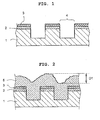
- Fig. 1 - Fig. 5 are schematic sectional views stepwisely showing formation steps of a shallow trench isolation region in a production process of a semiconductor device.
- Figs. 1 - 5 show that one part of a semiconductor device is formed in a substrate (wafer).
- plural semiconductor devices having a shallow trench isolation region are prepared for one substrate, and separated into individual semiconductor devices (chips) by dicing.
- the size of each part in the drawings was set to facilitate understanding and the size ratio between each part and each part does not necessarily match the actual ratio.
- a stopper film 3 is laminated on an oxidized insulating film 2 (silicon oxide and the like) on the surface of substrate 1.
- a resist film (not shown) is laminated by photolithography on the substrate 1 on which oxidized insulating film 2 and stopper film 3 are laminated and, after etching, the resist film is removed to form a trench 4 (etched part) ( Fig. 1 ).
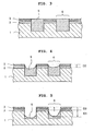
- An insulating film 5 (silicon oxide and the like) is laminated by CVD and the like to fill the trench 4 ( Fig. 2 ). In CMP of substrate 1 on which the insulating film 5 is laminated, it is ideal to flatly polish stopper film 3 and insulating film 5 to form a flat shallow trench isolation region 6 ( Fig. 3 ).
- a substrate has waviness, it is actually difficult to uniformly polish the whole substrate.
- insulating film 5 filled in trench 4 is further polished (excess polishing) in a part of the stopper film 3 which is exposed in an early stage.
- the level difference further grows ( Fig. 5 ).
- D3 shows an amount of increase in level difference caused by excessive polishing.
- a slurry for CMP containing a water-soluble organic compound such as polyacrylic acid, a salt thereof and the like, which is described in patent documents 1 - 3, and a slurry for CMP further containing polyvinylpyrrolidone and the like in combination are not necessarily satisfactory to minimize difference between levels of an insulating film and a stopper film.
- a slurry for CMP described in patent document 4 no suggestion is given as to minimization of difference between levels of an insulating film and a stopper film and, as far as the present inventors have confirmed, these slurries for CMP cannot minimize difference between levels of an insulating film and a stopper film.
- the present invention aims to provide a slurry for CMP, which is superior in the planarization property of a polished film, and does not damage a polished film, particularly, a slurry for CMP, which can provide an extremely small difference between the levels of an insulating film formed from silicon oxide etc. and a stopper film formed from silicon nitride etc., in a shallow trench isolation region formation step, and a polishing method of a substrate.
- the present inventors have conducted intensive studies in an attempt to solve the above-mentioned problem and found that the planarization property of a polished film is improved by using, as a slurry for CMP, a composition containing a polishing abrasive grain (c), as well as a water-soluble clathrate compound (a) and a polymer compound (b) having an acidic group optionally in a salt form as a side chain and a specific molecular weight in specific amounts and, particularly, a polished film having an extremely small difference between the levels of an insulating film and a stopper film can be obtained in a shallow trench isolation region formation step.
- polymer compound (b) having an acidic group as a side chain means that "polymer compound (b) has an acidic group as a pendant group”.
- the present invention relates to [1] - [12] below.
- the slurry for CMP of the present invention is superior in the planarization property of the polished film on the substrate, can particularly afford a polished film having an extremely small difference between the levels of the insulating film and the stopper film by polishing an insulating film or an interlayer dielectric in the formation of a shallow trench isolation region, and can improve the yield of substrate production.
- the slurry for CMP of the present invention contains a water-soluble clathrate compound (a), a polymer compound (b) having an acidic group optionally in a salt form as a side chain, a polishing abrasive grain (c) and water (d).
- the component contained in the slurry for CMP of the present invention may be one kind only or a combination of two or more kinds thereof.
- the water-soluble clathrate compound a compound having solubility in water at 25°C of not less than 0.01 g/L is preferable.
- the solubility in water at 25°C is less than 0.01 g/L, the effects of reduction of the difference between the levels of the insulating film and the stopper film and suppression of increased level difference due to excessive polishing cannot be achieved.
- the solubility in water at 25°C is preferably not less than 0.1 g/L, more preferably not less than 0.5 g/L.
- the "clathrate compound” is a molecule having a cavity, and a generic term of compounds capable of incorporating other molecules (guest) in molecules thereof (host).
- host compound tubular or cyclic compounds such as cyclodextrin, crown ether and the like are well known. These compounds are known to be able to control the size of the guest molecule to be incorporated by the size of the cavity.
- a cyclic compound is preferable.
- Examples of the aforementioned water-soluble clathrate compound (a) include cyclic oligosaccharide and a derivative thereof, water-soluble porphyrin, water-soluble phthalocyanine, crown ether, water-soluble cyclophane, water-soluble calixarene and the like.
- a polymer containing the aforementioned cyclic oligosaccharide or a derivative thereof or the like as a unit can also be used as a water-soluble clathrate compound (a).
- cyclic oligosaccharide or a derivative thereof is preferable from the aspects of industrial availability and the like.
- One kind of the aforementioned cyclic oligosaccharide and a derivative thereof may be selected and used alone, or two or more kinds thereof may be selected and used in combination.
- cyclic oligosaccharide and a derivative thereof a compound wherein 5-20 monosaccharides are cyclized, irrespective of the binding positions, and a derivative thereof can be mentioned.
- Monosaccharides having a pyranose skeleton and/or a furanose skeleton can be used irrespective of the stereoisomer in D-form or L-form.
- Examples of the monosaccharide include allose, talose, gulose, glucose, altrose, mannose, galactose, idose, rhamnose, erythrose, threose, ribose, lyxose, xylose, arabinose and the like.
- cyclic oligosaccharide and a derivative thereof include cyclodextrin, cyclomannin, cycloawaodorin, isocyclomaltopentaose, isocyclomaltohexaose and derivatives thereof.
- ⁇ -Cyclodextrin, ⁇ -cyclodextrin, ⁇ -cyclodextrin, and derivatives thereof are preferable from the aspects of industrial availability and the like, and ⁇ -cyclodextrin and a derivative thereof, a derivative of ⁇ -cyclodextrin, and ⁇ -cyclodextrin and a derivative thereof are more preferable from the aspects of water-solubility.
- the aforementioned water-soluble clathrate compound (a) needs to be contained in a proportion of 0.001 mass % - 3 mass % of the total amount of the slurry.
- the content of the aforementioned water-soluble clathrate compound (a) is less than 0.001 mass % of the total amount of the slurry, the difference between the levels of the insulating film and the stopper film cannot be reduced, and the amount of increase in level difference due to excessive polishing increases.
- the polishing abrasive grain (c) tends to coagulate in the slurry for CMP.
- the content of the water-soluble clathrate compound (a) is more preferably 0.01 mass % - 2.5 mass %, further preferably 0.05 mass % - 2 mass %, of the total amount of the slurry.
- the aforementioned water-soluble clathrate compound (a) preferably has a weight average molecular weight of 200 - 1,000,000.
- the aforementioned molecular weight is less than 200, the difference between the levels of the insulating film and the stopper film cannot be reduced, and when it exceeds 1,000,000, the viscosity of the slurry for CMP increases and the inflow property of the slurry for CMP decreases during polishing, thus sometimes resulting in low polishing uniformity.
- the weight average molecular weight of water-soluble clathrate compound (a) is more preferably 500 - 400,000, further preferably 700 - 50,000, to provide good action and effect as a slurry for CMP, from the aspects of reduction of difference between the levels of the insulating film and the stopper film and polishing uniformity.
- the aforementioned weight average molecular weight is a value obtained by connecting GPC column ("GMPWXL” manufactured by Tosoh Corporation) with a GPC apparatus ("150C” manufactured by Waters), measuring by using 200 mM aqueous phosphate solution as a mobile phase, converting the value based on the polyethylene glycol standard.
- the aforementioned polymer compound (b) needs to have a weight average molecular weight of not less than 1,000 and less than 1,000,000.
- the weight average molecular weight of the aforementioned polymer compound (b) is less than 1,000, the difference between the levels of the insulating film and the stopper film can not be reduced, and the amount of increase in level difference due to excessive polishing increases.
- the weight average molecular weight of the aforementioned polymer compound (b) is not less than 1,000,000, the polishing rate and polishing uniformity decrease.
- the weight average molecular weight of the aforementioned polymer compound (b) is more preferably 2,000 - 700,000, further preferably 3,000 - 400,000, from the aspects of polishing rate and polishing uniformity.
- the weight average molecular weight is a value obtained by connecting GPC column ("GMPWXL” manufactured by Tosoh Corporation) with a GPC apparatus ("150C” manufactured by Waters), measuring by using 200 mM aqueous phosphate solution as a mobile phase, converting the value based on the polyethylene glycol standard.
- the aforementioned polymer compound (b) needs to be contained in a proportion of 0.12 mass % - 3 mass % of the total amount of the slurry.
- the content of the aforementioned polymer compound (b) is less than 0.12 mass % of the total amount of the slurry, the difference between the levels of the insulating film and the stopper film cannot be reduced, and the amount of increase in level difference due to excessive polishing increases.
- the content of the aforementioned polymer compound (b) exceed 3 mass % of the total amount of the slurry, the polishing abrasive grain (c) tends to coagulate in the slurry for CMP.
- the content of the aforementioned polymer compound (b) is more preferably 0.14 mass % - 1 mass %, further preferably 0.16 mass % - 0.8 mass %, of the total amount of the slurry.
- Examples of the acidic group of the aforementioned polymer compound (b) include a phosphono group (-P(O) (OH) 2 , also referred to as a "phosphoric acid group”), a sulfo group (-SO 3 H also referred to as a “sulfonic acid group”), a carboxy group (-COOH) and the like.
- the acidic group may be in a salt form. Since interaction with the water-soluble clathrate compound (a) is superior, the aforementioned polymer compound (b) is preferably one having a carboxy group optionally in a salt form as a side chain.
- Examples of the salt of the acidic group that the aforementioned polymer compound (b) has as a side chain include alkali metal salts such as sodium salt, potassium salt, lithium salt and the like; alkaline earth metal salts such as magnesium salt, calcium salt and the like; amine salt; and ammonium salt. To suppress metal contamination in a semiconductor production step, amine salt and ammonium salt are preferable.
- primary amine, secondary amine and tertiary amine can be used, and more specifically, methylamine, dimethylamine, trimethylamine, ethylamine, diethylamine, triethylamine, n-butylamine, di-n-butylamine, tri-n-butylamine, isopropylamine and the like can be mentioned.
- the aforementioned polymer compound (b) preferably contains polymer (b-1) wherein the unit amount of (meth)acrylic acid and/or a salt thereof (hereinafter sometimes abbreviated as "(meth)acrylic acid (salt)")in the polymer is not less than 25 mass %, and the aforementioned polymer compound (b) is more preferably the aforementioned polymer (b-1).
- the polymer (b-1) wherein the unit amount of (meth)acrylic acid (salt) is not less than 25 mass % can show a good interaction with the aforementioned water-soluble clathrate compound (a).
- the unit amount of (meth)acrylic acid (salt) in the polymer (b-1) is preferably not less than 50 mass %, more preferably not less than 75 mass %, further preferably not less than 85 mass %, most preferably 100 mass %.
- the polymer compound (b) is preferably one or more kinds selected from the group consisting of them.
- the aforementioned polymer (b-1) can contain a unit other than (meth)acrylic acid (salt) (abbreviated as "other unit") in an amount of 75 mass % or below of the polymer.
- salt salt
- other unit those derived from a monomer having an unsaturated double bond can be mentioned.
- Examples of the aforementioned monomer having the unsaturated double bond include vinyl acetate, carboxylic acids such as itaconic acid, fumaric acid, maleic acid and the like and the salts thereof; acrylic esters such as methyl acrylate, ethyl acrylate, propyl acrylate, butyl acrylate, pentyl acrylate, hexyl acrylate, heptyl acrylate, octyl acrylate and the like; methacrylic esters such as methyl methacrylate, ethyl methacrylate, propyl methacrylate, butyl methacrylate, pentyl methacrylate, hexyl methacrylate, heptyl methacrylate, octyl methacrylate, 2-hydroxyethyl methacrylate and the like; sulfonic acids such as vinyl sulfonic acid, styrene sulfonic acid and the like and the salts thereof
- the aforementioned polymer compound (b) is preferably a polymer consisting of (meth)acrylic acid and/or a salt thereof alone.
- an arbitrarily proportion of one or more kinds selected from (meth)acrylic acid and the salts thereof can be polymerized.
- the aforementioned polymer compound (b) is preferably one or more kinds selected from the group consisting of polyacrylic acid, salt of polyacrylic acid with ammonium, salt of polyacrylic acid with amine, polymethacrylic acid, salt of polymethacrylic acid with ammonium and salt of polymethacrylic acid with amine, more preferably one or more kinds selected from the group consisting of salt of polyacrylic acid with ammonium and salt of polyacrylic acid with amine.
- the aforementioned polishing abrasive grain (c) is preferably fine particles having an average particle size of 0.5 nm - 1,000 nm.
- the average particle size of the aforementioned polishing abrasive grain (c) is less than 0.5 nm, the polishing rate may decrease, and when the average particle size exceeds 1,000 nm, the polishing flaw tends to develop.
- the average particle size of the aforementioned polishing abrasive grain (c) is more preferably 1 nm - 700 nm, further preferably 5 nm - 500 nm.
- the average particle size of the aforementioned polishing abrasive grain (c) can be measured by dynamic light scattering by using a particle size measuring apparatus ("Zeta-potential & Particle-size Analyzer ELSZ-2" manufactured by Otsuka Electronics Co., Ltd. etc.).
- an organic compound As the aforementioned polishing abrasive grain (c), an organic compound, a polymer compound, an inorganic compound and an organic-inorganic composite material can be used.
- organic compound and polymer compound are not particularly limited, for example, a fullerene derivative, and polymer compound particles obtained by polymerizing one or a combination of plural monomers having an unsaturated double bond, such as polystyrene particles, polyethylene particles, polyacrylic acid particles, polymethacrylic acid particles, polyacrylamide particles, polymethacrylamide particles and the like, and the like can be mentioned.
- Examples of the aforementioned inorganic compound include compounds such as fullerene, nanodiamond, silicon, germanium, silicon oxide, germanium oxide, metal, metal compound (e.g., metal oxide, metal sulfide, metal chloride, metal carbonate, metal sulfate, metal nitrate, metal fluoride, metal bromide, metal nitride, metal iodide), gallium arsenide, zinc selenide, cadmium tellurium and the like.
- metal compound e.g., metal oxide, metal sulfide, metal chloride, metal carbonate, metal sulfate, metal nitrate, metal fluoride, metal bromide, metal nitride, metal iodide
- gallium arsenide zinc selenide, cadmium tellurium and the like.
- lithium, sodium, potassium, magnesium, calcium, aluminum, gallium, indium, zinc, cadmium, copper, silver, gold, nickel, palladium, cobalt, rhodium, iron, manganese, chrome, molybdenum, tungsten, vanadium, niobium, tantalum, titanium, cerium, lanthanum, yttrium, iridium, zirconium, tin and the like can be mentioned. They can be used alone or a combination of plural kinds thereof.
- organic-inorganic composite material examples include inorganic compound particles coated with an organic compound, organic compound particles coated with an inorganic compound, inorganic compound particles dispersed in organic compound particles, organic polysiloxane compound and the like.
- the aforementioned inorganic compound particles are preferably used as the polishing abrasive grain (c).
- Respective particles of aluminum oxide, cerium oxide, fumed silica, colloidal silica, zirconium oxide, titanium oxide, tin oxide, germanium oxide, magnesium oxide and manganese oxide are more preferable, and cerium oxide particles are more preferable, from among the aforementioned inorganic compound particles, since they have a high polishing rate and are superior in the reduction of polishing flaws.
- the content of the polishing abrasive grain (c) is preferably 0.1 mass % - 30 mass %, more preferably 0.2 mass % - 25 mass %, particularly preferably 0.3 mass % - 20 mass %, of the total amount of the slurry.
- the content of the aforementioned polishing abrasive grain (c) is most preferably 0.5 mass % - 15 mass %.
- the slurry for CMP of the present invention can contain a known dispersant to improve the dispersion stability of a polishing abrasive grain.
- Examples of the aforementioned dispersant include water-soluble anionic dispersant, water-soluble nonionic dispersant, water-soluble cationic dispersant, water-soluble ampholytic dispersant and the like.
- Examples of the aforementioned water-soluble anionic dispersant include polyacrylic acid, polymethacrylic acid, polystyrene sulfonic acid, polysulfonic acid etc., and the salts thereof, which do not fall under the aforementioned polymer compound (b).
- Examples of the aforementioned water-soluble nonionic dispersant include polyvinyl alcohol, polyvinyl butyral, polyethylene glycol, polyvinylpyrrolidone, polyacrylamide, polymethacrylamide, N-substituted polyacrylamide, N,N-substituted polyacrylamide and the like, and examples of the water-soluble cationic dispersant include polyethyleneimine, polyallylamine and the like.
- Examples of the aforementioned water-soluble ampholytic dispersant include a copolymer obtained by polymerizing a cationic monomer having an unsaturated double bond and an anionic monomer having an unsaturated double bond, betaine having an anion and a cation on each terminal and the like. In the present invention, one or more kinds of dispersants selected from those can be used.
- the slurry for CMP of the present invention may contain an anionic polymer compound, a nonionic polymer compound, a cationic polymer compound, an ampholytic polymer compound and polysaccharides as long as the effect of the present invention is not inhibited.
- polyacrylic acid polymethacrylic acid, polystyrene sulfonic acid, polysulfonic acid etc., and salts thereof and the like, which do not fall under the aforementioned polymer compound (b)
- nonionic polymer compound polyvinyl alcohol, polyvinyl butyral, polyethylene glycol, polyvinylpyrrolidone, polyacrylamide, polymethacrylamide, N-substituted polyacrylamide, N,N-substituted polyacrylamide, polyoxyethylenelauryl ether, polyoxyethylenecetyl ether, polyoxyethylenestearyl ether, polyoxyethyleneoleyl ether and the like can be mentioned.
- aforementioned cationic polymer compound polyethyleneimine, polyallylamine and the like can be mentioned and, as the aforementioned ampholytic polymer compound, a copolymer obtained by polymerizing a cationic monomer having an unsaturated double bond and an anionic monomer having an unsaturated double bond and the like can be mentioned.
- the aforementioned polysaccharides include dextran, glycogen, amylose, amylopectin, heparin, agarose and the like.
- the slurry for CMP of the present invention may contain a low-molecular-weight compound having a molecular weight of 10 - 1,000 as long as the effect of the present invention is not inhibited.
- the low-molecular-weight compound include amines such as ethylamine, diethylamine, triethylamine, pyridine, piperazine, imidazole, butylamine, dibutylamine, isopropylamine, N,N-dimethylethanolamine, N,N-diethylethanolamine, aminoethylethanolamine and the like; alcohols such as methanol, ethanol, 1-propanol, 2-propanol, ethylene glycol and the like; carboxylic acids such as formic acid, acetic acid, butyric acid, propionic acid, malonic acid, succinic acid, fumaric acid, maleic acid, phthalic acid, salicylic acid, acrylic acid, methacrylic acid and the like; amino acids such as gly
- a composite of the aforementioned water-soluble clathrate compound (a) and the aforementioned polymer compound (b) can be formed by using them in combination.
- the aforementioned composite has high adsorptivity to a substrate, and can effectively form an adsorption film on a substrate.
- the adsorption film shows an improved protective action on the concave part of the substrate as compared to the use of polymer compound (b) alone, and therefore, only the convex part is effectively polished.
- the slurry for CMP of the present invention is considered to achieve good planarization property.
- the convex part can be selectively polished and good reduction of the level difference can be achieved by using the slurry for CMP of the present invention containing both the aforementioned water-soluble clathrate compound (a) and the aforementioned polymer compound (b).
- water-soluble polymer compounds e.g., polyacrylic acid etc.
- water (d) is not particularly limited, and distilled water, deionized water and the like can be preferably used.
- the content of water (d) is the amount obtained by subtracting the content of essential components (water-soluble clathrate compound (a), polymer compound (b), and polishing abrasive grain (c)), and optional component (for example, dispersant) from the slurry for CMP.
- the slurry for CMP of the present invention is preferably adjusted to a desired pH and used for polishing.
- the pH adjuster an acid or a base can be used.
- the acid hydrochloric acid and the like can be mentioned.
- a base aqueous ammonia or organic amine is preferably used rather than alkali metal hydroxide, thereby to prevent metal contamination in semiconductor polishing.
- the slurry for CMP of the present invention preferably has pH 3 - 12.5.
- the pH of the slurry for CMP is less than 3, the polishing rate decreases, and when it exceeds 12.5, the flatness of the insulating film on a substrate tends to decrease.
- the pH of the slurry for CMP of the present invention is more preferably 3.3 - 12, further preferably 3.5 - 11.7.
- the pH of a slurry for CMP can be measured, for example, by a pH meter ("pH meter F22" manufactured by Horiba, Ltd., etc.) according to a conventional method.
- the slurry for CMP of the present invention can be prepared, for example, as a three-liquid type slurry for CMP consisting of an aqueous solution of a water-soluble clathrate compound (a), an aqueous solution of a polymer compound (b), and a slurry of polishing abrasive grain (c).
- it can also be prepared as a two-liquid type slurry for CMP consisting of a slurry containing polished abrasive grain (c) or a slurry obtained by mixing aqueous solution of water-soluble clathrate compound (a) and polishing abrasive grain (c), and an aqueous mixed solution water-soluble clathrate compound (a) and polymer compound (b); a two-liquid type slurry for CMP consisting of a slurry of a mixture of polishing abrasive grain (c) and water-soluble clathrate compound (a), and an aqueous solution of polymer compound (b); or a two-liquid type slurry for CMP consisting of a slurry of a mixture of polishing abrasive grain (c) and polymer compound (b), and an aqueous solution of water-soluble clathrate compound (a).
- it can also be prepared as a one-liquid type slurry for CMP consisting of an aqueous solution of a mixture of water-soluble clathrate compound (a), polymer compound (b) and polishing abrasive grain (c).
- a water-soluble clathrate compound
- b polymer compound
- c polishing abrasive grain
- the formulation of each component can be freely changed when in use, and therefore, the planarization property, polishing rate and level difference elimination property can be easily controlled.
- a method including feeding a slurry containing polishing abrasive grain (c), and an aqueous mixed solution of water-soluble clathrate compound (a) and polymer compound (b) through separate pipings, joining these pipings to mix them immediately before the outlet of the supply piping and supplying the mixture on a polishing pad, a method including mixing a slurry containing polishing abrasive grain (c), with an aqueous mixed solution of water-soluble clathrate compound (a) and polymer compound (b) immediately before polishing and the like are employed.
- polishing is performed with a two-liquid type or three-liquid type slurry
- the polishing method of the present invention is characterized by pressing a substrate with a film formed thereon to be polished against a polishing pad adhered onto a polishing surface plate with a double sided tape, a hook-and-loop fastener and the like, applying a pressure thereon, and relatively moving the substrate and the polishing pad while supplying the slurry for CMP of the present invention between the substrate and the polishing pad to polish the film to be polished.
- the polishing method of a substrate of the present invention is explained below by referring to a semiconductor substrate having a silicon oxide film, which is an inorganic insulating film, formed thereon.
- a general polishing apparatus having a polishing surface plate to which a polishing pad can be attached, and equipped with a motor whose rotation number can be changed, and the like, and a holder capable of holding a substrate having a film to be polished and the like can be used.
- the polishing condition is not particularly limited, for efficiently polishing, a surface plate and a substrate each preferably show a low rotation number of 300 rpm or below
- the pressure to be applied to a substrate is preferably not more than 150 kPa to prevent development of flaw after polishing.
- a semiconductor substrate after the completion of polishing is preferably washed well with running water, and dried by removing water drops attached to a semiconductor substrate by a spin dryer and the like.
- an aluminum wiring or copper wiring is formed on the inorganic insulating film, an inorganic insulating film is formed between and on the wirings by the below-mentioned method, and the film is similarly polished with a slurry for CMP to give a flat surface. This step is repeated a given number of times, whereby a semiconductor substrate having a desired number of layers can be produced.
- polishing pad that can be used in the present invention is not particularly limited, for example, general non-woven fabric, woven fabric, artificial leather, synthetic resin and the like can be mentioned. Of these, a synthetic resin is preferably used.
- thermosetting polyurethane resin examples include thermosetting polyurethane resin; thermoplastic polyurethane resin; epoxy resin; fluorine resin; polyolefin resins such as polyethylene resin, polypropylene, resin and the like; crosslinked rubbers such as polybutadiene resin, polystyrene butadiene resin and the like; acrylic resins such as polyacrylic acid resin, polymethacrylic acid resin, polymethyl methacrylate resin and the like; vinyl resins such as polyvinyl alcohol resin, polyvinyl butyral resin, ethylenevinyl acetate copolymer resin and the like; and the like.
- the aforementioned synthetic resins may be used alone, or plural kinds thereof may be used in combination, with addition of additives and the like. In view of abrasive resistance, a polyurethane resin is preferable.
- the aforementioned synthetic resin is not particularly limited, it may be a porous material.
- the production method of a porous material include a method of dispersing a fine hollow body in a synthetic resin, a method of forming a substantially porous material by dispersing a water-soluble polymer compound alone or plural kinds thereof in combination in a synthetic resin to allow elution of the aforementioned water-soluble polymer compound by a slurry for CMP during polishing, a method using supercritical foam molding, a method of sintering fine particles of a polymer compound to form a continuous pore structure and the like.
- the structure of the aforementioned polishing pad is not particularly limited, and it may be a single layer structure or a multi layer structure having a cushion layer.
- the aforementioned polishing pad is preferably processed to have a hole structure and/or a groove structure to pool a slurry for CMP.
- the groove structure is not subject to any particular limitation, it may have a grid shape, a radial shape, a helicoid shape, a concentric shape or the like.
- the aforementioned groove structure and hole structure may be alone or plural kinds thereof may be used in combination.
- the aforementioned polishing pad may have a structure wherein an abrasive grain is contained in a polishing pad.
- a method including mixing an abrasive grain, a synthetic resin and a solvent, injecting the mixture in a molding tool and drying same, or a method including mixing molten synthetic resin and an abrasive grain, injecting the mixture in a molding tool and cooling same can be used.
- a conditioner for CMP wherein diamond particles are fixed on the surface of a carrier by nickel electrodeposition and the like is attached to a polishing apparatus, the aforementioned conditioner is pressed against the polishing pad, and the surface of the aforementioned polishing pad can be controlled to have a surface roughness preferable for polishing an insulating film which is a film to be polished.
- the slurry for CMP of the present invention can be applied not only to a silicon oxide film formed on a semiconductor substrate but also production processes of various semiconductor devices, MEMS (Micro Electro Mechanical Systems) and the like, and the like.
- the slurry for CMP of the present invention can be used for polishing an inorganic insulating film such as silicon oxide film, glass film, silicon nitride film and the like, which is formed on a wiring board having a given wiring; a film mainly containing polysilicon, aluminum, copper, titanium, titanium nitride, tungsten, tantalum, tantalum nitride and the like; optical glass such as photomask, lens, prism and the like; an inorganic conductive film such as tin-doped indium oxide (ITO) and the like; optical monocrystal for an optical integrated circuit composed of glass and crystal materials, optical switching element, optical waveguide, end face of optical fiber, scintillator and the like; solid laser monocrystal; sapphire substrate
- the slurry for CMP of the present invention can be preferably used for polishing of, particularly, an insulating film in the formation of a shallow trench isolation region.
- Cerium oxide abrasive grain slurry (abrading agent "GPL-C1010" manufactured by Showa Denko K.K., content of cerium oxide abrasive grain in slurry 10 mass%, 50 g), ⁇ -cyclodextrin (manufactured by Wako Pure Chemical Industries, Ltd., 0.5 g), polyacrylic acid (manufactured by Wako Pure Chemical Industries, Ltd., weight average molecular weight 5,000, 2.5 g) and distilled water were mixed in a 1 L measuring cylinder. While stirring with a magnetic stirrer, 28 mass% aqueous ammonia (manufactured by Wako Pure Chemical Industries, Ltd.) was added to adjust the mixture to pH 5.0. Distilled water was added to the total amount of 1,000 g to give a slurry for CMP (abrasive grain content 0.5 mass%, ⁇ -cyclodextrin content 0.05 mass%, polyacrylic acid content 0.25 mass%).
- CMP
- Example 2 In the same manner as in Example 1 except that ⁇ -cyclodextrin (manufactured by Wako Pure Chemical Industries, Ltd., 1.5 g) (content 0.15 mass%) was used, a slurry for CMP was prepared.
- Example 2 In the same manner as in Example 1 except that ⁇ -cyclodextrin (manufactured by Wako Pure Chemical Industries, Ltd., 3.0 g) (content 0.3 mass%) was used, a slurry for CMP was prepared.
- ⁇ -cyclodextrin manufactured by Wako Pure Chemical Industries, Ltd., 3.0 g
- Example 2 In the same manner as in Example 1 except that ⁇ -cyclodextrin (manufactured by Wako Pure Chemical Industries, Ltd., 3.0 g) (content 0.3 mass%) and polyacrylic acid (manufactured by Wako Pure Chemical Industries, Ltd., weight average molecular weight 25,000, 2.5 g) (content 0.25 mass%) as a polymer compound were used, a slurry for CMP was prepared.
- Example 2 In the same manner as in Example 1 except that ⁇ -cyclodextrin (manufactured by Wako Pure Chemical Industries, Ltd., 3.0 g) (content 0.3 mass%) and polyacrylic acid (manufactured by Wako Pure Chemical Industries, Ltd., weight average molecular weight 250,000, 2.5 g) (content 0.25 mass%) as a polymer compound were used, a slurry for CMP was prepared.
- Example 2 In the same manner as in Example 1 except that ⁇ -cyclodextrin (manufactured by Wako Pure Chemical Industries, Ltd., 3.0 g) (content 0.3 mass%) and polymethacrylic acid (manufactured by polyscience, weight average molecular weight 100,000, 2.5 g) (content 0.25 mass%) as a polymer compound were used, a slurry for CMP was prepared.
- ⁇ -cyclodextrin manufactured by Wako Pure Chemical Industries, Ltd., 3.0 g
- polymethacrylic acid manufactured by polyscience, weight average molecular weight 100,000, 2.5 g
- Example 2 In the same manner as in Example 1 except that ⁇ -cyclodextrin (manufactured by Wako Pure Chemical Industries, Ltd., 3.0 g) (content 0.3 mass%) was used as a water-soluble clathrate compound, a slurry for CMP was prepared. -
- Example 2 In the same manner as in Example 1 except that ⁇ -cyclodextrin (manufactured by Wako Pure Chemical Industries, Ltd., 3.0 g) (content 0.3 mass%) was used as a water-soluble clathrate compound, a slurry for CMP was prepared.
- ⁇ -cyclodextrin manufactured by Wako Pure Chemical Industries, Ltd., 3.0 g
- Example 2 In the same manner as in Example 1 except that methyl- ⁇ -cyclodextrin (manufactured by Wako Pure Chemical Industries, Ltd., 4.5 g) (content 0.45 mass%) was used as a water-soluble clathrate compound, a slurry for CMP was prepared.
- Example 2 In the same manner as in Example 1 except that ⁇ -cyclodextrin (manufactured by Wako Pure Chemical Industries, Ltd., 1.5 g) (content 0.15 mass%), polyacrylic acid (manufactured by Wako Pure Chemical Industries, Ltd., weight average molecular weight 5,000, 1.5 g) (content 0.15 mass%) and cerium oxide abrasive grain slurry (the aforementioned GPL-C1010, 1.5 g) (content 0.15 mass%) were used, a slurry for CMP was prepared.
- ⁇ -cyclodextrin manufactured by Wako Pure Chemical Industries, Ltd., 1.5 g
- polyacrylic acid manufactured by Wako Pure Chemical Industries, Ltd., weight average molecular weight 5,000, 1.5 g) (content 0.15 mass%)
- cerium oxide abrasive grain slurry the aforementioned GPL-C1010, 1.5 g
- Example 2 In the same manner as in Example 1 except that ⁇ -cyclodextrin (manufactured by Wako Pure Chemical Industries, Ltd.) was not added, a slurry for CMP was prepared.
- ⁇ -cyclodextrin manufactured by Wako Pure Chemical Industries, Ltd.
- Example 2 In the same manner as in Example 1 except that ⁇ -cyclodextrin (manufactured by Wako Pure Chemical Industries, Ltd.) was not added, and polyacrylic acid (manufactured by Wako Pure Chemical Industries, Ltd., weight average molecular weight 25,000, 2.5 g) (content 0.25 mass%) was used as a polymer compound, a slurry for CMP was prepared.
- ⁇ -cyclodextrin manufactured by Wako Pure Chemical Industries, Ltd.
- polyacrylic acid manufactured by Wako Pure Chemical Industries, Ltd., weight average molecular weight 25,000, 2.5 g
- Example 2 In the same manner as in Example 1 except that ⁇ -cyclodextrin (manufactured by Wako Pure Chemical Industries, Ltd.) was not added, and polyacrylic acid (manufactured by Wako Pure Chemical Industries, Ltd., weight average molecular weight 250,000, 2.5 g) (content 0.25 mass%) was used as a polymer compound, a slurry for CMP was prepared.
- ⁇ -cyclodextrin manufactured by Wako Pure Chemical Industries, Ltd.
- polyacrylic acid manufactured by Wako Pure Chemical Industries, Ltd., weight average molecular weight 250,000, 2.5 g
- Example 2 In the same manner as in Example 1 except that ⁇ -cyclodextrin (manufactured by Wako Pure Chemical Industries, Ltd., 1.0 g) (content 0.1 mass%) and polyacrylic acid (manufactured by Wako Pure Chemical Industries, Ltd., weight average molecular weight 5,000, 1.0 g) (content 0.1 mass%) were used, a slurry for CMP was prepared.
- Example 2 In the same manner as in Example 1 except that ⁇ -cyclodextrin (manufactured by Wako Pure Chemical Industries, Ltd., 1.0 g) (content 0.1 mass%) and polyacrylic acid (manufactured by Wako Pure Chemical Industries, Ltd., weight average molecular weight 250,000, 1.0 g) (content 0.1 mass%) as a polymer compound were used, a slurry for CMP was prepared.
- Example 2 In the same manner as in Example 1 except that dextran (manufactured by Wako Pure Chemical Industries, Ltd., 3.0 g) (content 0.3 mass%) was used instead of ⁇ -cyclodextrin, a slurry for CMP was prepared.
- Example 2 In the same manner as in Example 1 except that ⁇ -cyclodextrin (manufactured by Wako Pure Chemical Industries, Ltd., 3.0 g) (content 0.3 mass%) and polyacrylamide (manufactured by Wako Pure Chemical Industries, Ltd., weight average molecular weight 5,000, 2.5 g) (content 0.25 mass%) as a polymer compound were used, a slurry for CMP was prepared.
- ⁇ -cyclodextrin manufactured by Wako Pure Chemical Industries, Ltd., 3.0 g
- polyacrylamide manufactured by Wako Pure Chemical Industries, Ltd., weight average molecular weight 5,000, 2.5 g
- Example 7 In the same manner as in Example 7 except that polyacrylic acid (manufactured by KANTO CHEMICAL CO., INC., weight average molecular weight 1,080,000, 2.5 g) (content 0.25 mass%) was used as a polymer compound, a slurry for CMP was prepared.
- polyacrylic acid manufactured by KANTO CHEMICAL CO., INC., weight average molecular weight 1,080,000, 2.5 g
- the average particle size of the polishing abrasive grain (c) used for respective slurries for CMP of the aforementioned Examples and Comparative Examples was measured.
- pH of each slurry for CMP was measured.
- an insulating film was polished, and the difference between the levels of the insulating film and the stopper film was measured.
- the measurement method for the average particle size of polishing abrasive grain (c), the measurement method for slurry for CMP, and the measurement method for the difference between the levels of an insulating film and a stopper film are described below.
- pH meter F22 manufactured by Horiba, Ltd. and a standard buffer (phthalate pH buffer; pH 4.00 (25°C), neutral phosphate pH buffer; pH 7.00 (25°C), borate pH buffer; pH 9.00 (25°C)
- a standard buffer phthalate pH buffer; pH 4.00 (25°C), neutral phosphate pH buffer; pH 7.00 (25°C), borate pH buffer; pH 9.00 (25°C)
- a patterned wafer "SKW3-2" manufactured by SKW was used as a test substrate.
- the aforementioned wafer includes, as shown in Fig. 2 , oxidized insulating film 2 (silicon oxide), stopper film 3 (silicon nitride), trench 4 and insulating film 5 (silicon oxide) formed therein (thickness of oxidized insulating film 2: 10 nm, thickness of stopper film 3: 150 nm, width of stopper film 3: 100 ⁇ m, depth of trench 4 (distance from the surface of stopper film 3 to the bottom of trench 4): 500 nm, width of trench 4: 100 ⁇ m, average thickness of insulating film 5: 600 nm).
- the aforementioned wafer was fixed on a substrate-holding part of a polishing apparatus ("BC-15" manufactured by MAT).
- a 380 mm ⁇ polishing pad (“IC1400” manufactured by Rohm & Haas, concentric circular groove) was adhered to a polishing surface plate with a double-sided tape.
- a conditioner manufactured by A.L.M.T.
- the polishing surface plate was rotated at 100 rpm, the aforementioned wafer was rotated at 99 rpm in the same direction while supplying each slurry for CMP of the Examples and Comparative Examples on the aforementioned polishing pad at a flow rate of 120 mL/min, and the aforementioned wafer was pressed against the aforementioned polishing pad at load of 23.4 kPa to polish the aforementioned wafer.
- the time point when the insulating film 5 (silicon oxide) on the stopper film 3 (silicon nitride) disappeared to expose the stopper film 3 was taken as a "just polishing", at which the polishing was stopped.
- the wafer was washed with distilled water and dried.
- the thickness of the stopper film 3 and the insulating film 5 was measured.
- a surface-roughness measuring apparatus small surface roughness measuring apparatus "SJ-400” manufactured by Mitutoyo Corporation
- the wafer after just polishing was further polished excessively as shown in Fig. 5 , and the amount of increase in the level difference D3 was measured.
- the wafer after just polishing was further polished for the time corresponding to 15% of the polishing time from the start of the polishing to the just polishing, and the film thickness and level difference were measured in the same manner as in the above.
- Example 1 2 3 4 5 6 water-soluble clathrate compound (a) component ⁇ -cyclodextrin content (mass %) 0.05 0.15 0.3 0.3 0.3 0.3 polymer compound (b) component polyacrylic acid polymethacrylic acid weight average molecular weight 5000 5000 5000 25000 250000 100000 content (mass %) 0.25 0.25 0.25 0.25 0.25 0.25 0.25 0.25 0.25 polishing abrasive grain (c) component cerium oxide content (mass %) 0.5 pH 5.0 5.0 4.9 5.0 5.0 polishing time (sec) 213 199 205 218 231 225 just polishing level difference D2 (nm) 25 25 20 30 40 30 15%-over polishing level difference (nm) 39 31 23 36 46 40 amount of increase in level difference D3 (nm) 14 6 3 6 6 10 10
- the present invention provides a slurry for CMP applicable to silicon oxide film formed on a semiconductor substrate, and production processes of various semiconductor devices, and a polishing method of a substrate.
- the slurry for CMP of the present invention is particularly suitable for polishing an insulating film and an interlayer dielectric in the formation of a shallow trench isolation region, can afford, in the aforementioned steps, a polished film having an extremely small difference between the levels of the insulating film and the stopper film, and can improve the yield of substrate production.
Applications Claiming Priority (2)
| Application Number | Priority Date | Filing Date | Title |
|---|---|---|---|
| JP2009258444 | 2009-11-11 | ||
| PCT/JP2010/069851 WO2011058952A1 (ja) | 2009-11-11 | 2010-11-08 | 化学的機械的研磨用スラリー並びにそれを用いる基板の研磨方法 |
Publications (3)
| Publication Number | Publication Date |
|---|---|
| EP2500929A1 true EP2500929A1 (de) | 2012-09-19 |
| EP2500929A4 EP2500929A4 (de) | 2013-08-14 |
| EP2500929B1 EP2500929B1 (de) | 2018-06-20 |
Family
ID=43991611
Family Applications (1)
| Application Number | Title | Priority Date | Filing Date |
|---|---|---|---|
| EP10829911.6A Active EP2500929B1 (de) | 2009-11-11 | 2010-11-08 | Schlamm für chemisch-mechanisches polieren und verfahren zum polieren von substraten damit |
Country Status (8)
| Country | Link |
|---|---|
| US (1) | US9536752B2 (de) |
| EP (1) | EP2500929B1 (de) |
| JP (1) | JP5878020B2 (de) |
| KR (1) | KR101359092B1 (de) |
| CN (1) | CN102666760B (de) |
| IL (1) | IL219703A (de) |
| TW (1) | TWI570226B (de) |
| WO (1) | WO2011058952A1 (de) |
Cited By (2)
| Publication number | Priority date | Publication date | Assignee | Title |
|---|---|---|---|---|
| EP3397710A4 (de) * | 2015-12-29 | 2019-08-28 | Cabot Microelectronics Corporation | Cmp-verarbeitungszusammensetzung mit alkylamin und cyclodextrin |
| EP3587525A1 (de) * | 2018-06-29 | 2020-01-01 | Versum Materials US, LLC | Chemisch-mechanisches polieren für niedriges oxid-trench-dishing |
Families Citing this family (49)
| Publication number | Priority date | Publication date | Assignee | Title |
|---|---|---|---|---|
| SG188621A1 (en) * | 2010-10-21 | 2013-04-30 | Moresco Corp | Lubricant composition for polishing glass substrates and polishing slurry |
| WO2012161202A1 (ja) * | 2011-05-24 | 2012-11-29 | 株式会社クラレ | 化学機械研磨用エロージョン防止剤、化学機械研磨用スラリーおよび化学機械研磨方法 |
| JP2012248594A (ja) * | 2011-05-26 | 2012-12-13 | Kyushu Institute Of Technology | 研磨剤 |
| JP2013074036A (ja) * | 2011-09-27 | 2013-04-22 | Toshiba Corp | Cmp用スラリーおよび半導体装置の製造方法 |
| JP5882024B2 (ja) * | 2011-11-01 | 2016-03-09 | 花王株式会社 | 研磨液組成物 |
| CN102585708A (zh) * | 2012-03-13 | 2012-07-18 | 上海华明高纳稀土新材料有限公司 | 稀土抛光材料及其制备方法 |
| US8916061B2 (en) * | 2012-03-14 | 2014-12-23 | Cabot Microelectronics Corporation | CMP compositions selective for oxide and nitride with high removal rate and low defectivity |
| JP5822356B2 (ja) * | 2012-04-17 | 2015-11-24 | 花王株式会社 | シリコンウェーハ用研磨液組成物 |
| JP5957292B2 (ja) * | 2012-05-18 | 2016-07-27 | 株式会社フジミインコーポレーテッド | 研磨用組成物並びにそれを用いた研磨方法及び基板の製造方法 |
| JP5840567B2 (ja) * | 2012-05-30 | 2016-01-06 | 株式会社クラレ | 化学機械研磨用エロージョン防止剤、化学機械研磨用スラリーおよび化学機械研磨方法 |
| EP2888077B8 (de) * | 2012-08-24 | 2017-09-27 | Ecolab USA Inc. | Verfahren zum polieren von oberflächen aus saphir |
| JP6015259B2 (ja) * | 2012-09-06 | 2016-10-26 | 旭硝子株式会社 | 情報記録媒体用ガラス基板の製造方法および磁気ディスクの製造方法 |
| US9896604B2 (en) | 2013-03-15 | 2018-02-20 | Ecolab Usa Inc. | Methods of polishing sapphire surfaces |
| EP3007213B1 (de) * | 2013-06-07 | 2020-03-18 | Fujimi Incorporated | Verwendung einer polierzusammensetzung für siliciumwafer |
| WO2015037311A1 (ja) | 2013-09-10 | 2015-03-19 | 日立化成株式会社 | スラリー、研磨液セット、研磨液、基体の研磨方法及び基体 |
| CN103756571A (zh) * | 2013-12-25 | 2014-04-30 | 上海华明高纳稀土新材料有限公司 | 稀土抛光粉及其制备方法 |
| CN104745092A (zh) * | 2013-12-26 | 2015-07-01 | 安集微电子(上海)有限公司 | 一种应用于sti领域的化学机械抛光液及其使用方法 |
| JP6389630B2 (ja) | 2014-03-31 | 2018-09-12 | ニッタ・ハース株式会社 | 研磨用組成物 |
| JP2015203080A (ja) * | 2014-04-15 | 2015-11-16 | 株式会社フジミインコーポレーテッド | 研磨用組成物 |
| TWI563073B (en) * | 2014-06-03 | 2016-12-21 | Cabot Microelectronics Corp | Cmp compositions and methods for polishing rigid disk surfaces |
| KR101686986B1 (ko) | 2014-07-28 | 2016-12-16 | 에스케이케미칼주식회사 | 류프로라이드를 포함하는 속효성과 지속성을 동시에 갖는 약제학적 조성물 |
| KR20160058342A (ko) * | 2014-11-14 | 2016-05-25 | 삼성전자주식회사 | 슬러리 화합물 |
| CN105802506B (zh) * | 2014-12-29 | 2020-06-09 | 安集微电子(上海)有限公司 | 一种化学机械抛光液 |
| US10109493B2 (en) * | 2015-01-12 | 2018-10-23 | Versum Materials Us, Llc | Composite abrasive particles for chemical mechanical planarization composition and method of use thereof |
| KR20170134963A (ko) * | 2015-03-30 | 2017-12-07 | 제이에스알 가부시끼가이샤 | 화학 기계 연마용 처리 조성물, 화학 기계 연마 방법 및 세정 방법 |
| JP6638208B2 (ja) * | 2015-04-02 | 2020-01-29 | 日立化成株式会社 | 研磨剤、研磨剤用貯蔵液及び研磨方法 |
| JP2016199659A (ja) * | 2015-04-09 | 2016-12-01 | 日立化成株式会社 | 研磨液、研磨液セット及び基体の研磨方法 |
| KR101682085B1 (ko) * | 2015-07-09 | 2016-12-02 | 주식회사 케이씨텍 | 텅스텐 연마용 슬러리 조성물 |
| KR102463863B1 (ko) * | 2015-07-20 | 2022-11-04 | 삼성전자주식회사 | 연마용 조성물 및 이를 이용한 반도체 장치의 제조 방법 |
| JP2017037178A (ja) | 2015-08-10 | 2017-02-16 | ルネサスエレクトロニクス株式会社 | 半導体装置およびその製造方法 |
| JP6510946B2 (ja) * | 2015-10-01 | 2019-05-08 | 豊田合成株式会社 | ポリロタキサンを含む組成物及びその利用物 |
| KR102605140B1 (ko) * | 2015-12-17 | 2023-11-24 | 솔브레인 주식회사 | 화학 기계적 연마 슬러리 조성물 및 이를 이용한 연마 방법 |
| KR102574842B1 (ko) * | 2015-12-17 | 2023-09-06 | 솔브레인 주식회사 | 화학 기계적 연마 슬러리 조성물 및 이를 이용한 연마 방법 |
| JP6697362B2 (ja) * | 2016-09-23 | 2020-05-20 | 株式会社フジミインコーポレーテッド | 表面処理組成物、ならびにこれを用いた表面処理方法および半導体基板の製造方法 |
| TWI673357B (zh) * | 2016-12-14 | 2019-10-01 | 美商卡博特微電子公司 | 自化學機械平坦化基板移除殘留物之組合物及方法 |
| US10955332B2 (en) | 2016-12-22 | 2021-03-23 | Illumina, Inc. | Flow cell package and method for making the same |
| US10377014B2 (en) | 2017-02-28 | 2019-08-13 | Ecolab Usa Inc. | Increased wetting of colloidal silica as a polishing slurry |
| SG11201909702YA (en) * | 2017-04-17 | 2019-11-28 | Nissan Chemical Corp | Polishing composition containing amphoteric surfactant |
| CN107353833B (zh) * | 2017-07-24 | 2020-05-12 | 包头天骄清美稀土抛光粉有限公司 | 高选择性浅槽隔离化学机械抛光浆料的制备工艺 |
| JP7045171B2 (ja) * | 2017-11-28 | 2022-03-31 | 花王株式会社 | 研磨液組成物 |
| KR102543679B1 (ko) * | 2017-11-30 | 2023-06-16 | 솔브레인 주식회사 | 화학적 기계적 연마 슬러리 조성물 및 이를 이용한 반도체 소자의 제조방법 |
| KR20190110662A (ko) * | 2018-03-20 | 2019-10-01 | 삼성디스플레이 주식회사 | 연마 슬러리 및 이를 이용한 기판 연마 방법 |
| KR20200010806A (ko) * | 2018-07-23 | 2020-01-31 | 삼성전자주식회사 | 연마 슬러리 및 그 제조 방법과 반도체 소자의 제조 방법 |
| KR20200109549A (ko) | 2019-03-13 | 2020-09-23 | 삼성전자주식회사 | 연마 슬러리 및 반도체 소자의 제조 방법 |
| JP7375450B2 (ja) | 2019-10-17 | 2023-11-08 | Jsr株式会社 | 半導体処理用組成物及び処理方法 |
| KR20210059507A (ko) * | 2019-11-15 | 2021-05-25 | 삼성전자주식회사 | 연마 슬러리 및 반도체 소자의 제조 방법 |
| CN113249035A (zh) * | 2020-02-10 | 2021-08-13 | 中国科学院长春光学精密机械与物理研究所 | 化学机械抛光液及其应用 |
| CN117561311A (zh) * | 2021-06-14 | 2024-02-13 | 恩特格里斯公司 | 硬质衬底研磨 |
| CN115011257B (zh) * | 2022-06-30 | 2023-12-19 | 万华化学集团电子材料有限公司 | 一种具有改善pou寿命的钨抛光液及其应用 |
Citations (6)
| Publication number | Priority date | Publication date | Assignee | Title |
|---|---|---|---|---|
| US6019806A (en) * | 1998-01-08 | 2000-02-01 | Sees; Jennifer A. | High selectivity slurry for shallow trench isolation processing |
| EP1148538A1 (de) * | 1998-12-25 | 2001-10-24 | Hitachi Chemical Company, Ltd. | Cmp-schleifmittel, flüssigzusatz für dasselbe und substratpoliermethode |
| US20020045350A1 (en) * | 1998-02-24 | 2002-04-18 | Showa Denko K.K. | Composition for polishing a semiconductor device and process for manufacturing a semiconductor device using the same |
| US20070210278A1 (en) * | 2006-03-08 | 2007-09-13 | Lane Sarah J | Compositions for chemical mechanical polishing silicon dioxide and silicon nitride |
| US20090176372A1 (en) * | 2007-12-27 | 2009-07-09 | Gaku Minamihaba | Chemical mechanical polishing slurry and semiconductor device manufacturing method |
| WO2009104517A1 (ja) * | 2008-02-18 | 2009-08-27 | Jsr株式会社 | 化学機械研磨用水系分散体および化学機械研磨方法 |
Family Cites Families (20)
| Publication number | Priority date | Publication date | Assignee | Title |
|---|---|---|---|---|
| DE69830676D1 (de) | 1997-01-10 | 2005-08-04 | Texas Instruments Inc | CMP Suspension mit hoher Selektivität |
| JP2002110596A (ja) * | 2000-10-02 | 2002-04-12 | Mitsubishi Electric Corp | 半導体加工用研磨剤およびこれに用いる分散剤、並びに上記半導体加工用研磨剤を用いた半導体装置の製造方法 |
| DE60332881D1 (de) * | 2002-04-30 | 2010-07-15 | Hitachi Chemical Co Ltd | Poliermittel und Polierverfahren |
| US20100009540A1 (en) * | 2002-09-25 | 2010-01-14 | Asahi Glass Company Limited | Polishing compound, its production process and polishing method |
| TW200613485A (en) * | 2004-03-22 | 2006-05-01 | Kao Corp | Polishing composition |
| JP4776269B2 (ja) | 2005-04-28 | 2011-09-21 | 株式会社東芝 | 金属膜cmp用スラリー、および半導体装置の製造方法 |
| US20110045741A1 (en) | 2005-04-28 | 2011-02-24 | Techno Semichem Co., Ltd. | Auto-Stopping Abrasive Composition for Polishing High Step Height Oxide Layer |
| JP2007013059A (ja) * | 2005-07-04 | 2007-01-18 | Adeka Corp | Cmp用研磨組成物 |
| US20070049180A1 (en) | 2005-08-24 | 2007-03-01 | Jsr Corporation | Aqueous dispersion for chemical mechanical polishing, kit for preparing the aqueous dispersion, chemical mechanical polishing process, and process for producing semiconductor devices |
| JP2007242839A (ja) | 2006-03-08 | 2007-09-20 | Adeka Corp | 金属cmp用研磨組成物 |
| US20070254485A1 (en) * | 2006-04-28 | 2007-11-01 | Daxin Mao | Abrasive composition for electrochemical mechanical polishing |
| CN101490814A (zh) * | 2006-10-06 | 2009-07-22 | Jsr株式会社 | 化学机械研磨用水系分散体及半导体装置的化学机械研磨方法 |
| JP5433936B2 (ja) | 2006-10-11 | 2014-03-05 | 日立化成株式会社 | 金属用研磨液とその製造方法及び金属用研磨液を用いた被研磨膜の研磨方法 |
| KR20100049626A (ko) | 2007-09-03 | 2010-05-12 | 제이에스알 가부시끼가이샤 | 화학 기계 연마용 수계 분산체 및 그의 제조 방법, 화학 기계 연마용 수계 분산체를 제조하기 위한 키트, 및 반도체 장치의 화학 기계 연마 방법 |
| JP2009224771A (ja) | 2008-02-18 | 2009-10-01 | Jsr Corp | 化学機械研磨用水系分散体およびその製造方法、ならびに化学機械研磨方法 |
| WO2009107472A1 (ja) * | 2008-02-27 | 2009-09-03 | Jsr株式会社 | 化学機械研磨用水系分散体およびそれを用いた化学機械研磨方法、化学機械研磨用水系分散体の再生方法 |
| JP4521058B2 (ja) | 2008-03-24 | 2010-08-11 | 株式会社Adeka | 表面改質コロイダルシリカおよびこれを含有するcmp用研磨組成物 |
| JP2009258579A (ja) * | 2008-03-26 | 2009-11-05 | Fujifilm Corp | 平版印刷版原版の製版方法 |
| JP5314329B2 (ja) * | 2008-06-12 | 2013-10-16 | 富士フイルム株式会社 | 研磨液 |
| JP2012109287A (ja) | 2009-03-13 | 2012-06-07 | Asahi Glass Co Ltd | 半導体用研磨剤、その製造方法及び研磨方法 |
-
2010
- 2010-11-08 JP JP2011540500A patent/JP5878020B2/ja active Active
- 2010-11-08 CN CN201080051174.0A patent/CN102666760B/zh active Active
- 2010-11-08 WO PCT/JP2010/069851 patent/WO2011058952A1/ja active Application Filing
- 2010-11-08 US US13/508,924 patent/US9536752B2/en active Active
- 2010-11-08 KR KR1020127014821A patent/KR101359092B1/ko active IP Right Grant
- 2010-11-08 EP EP10829911.6A patent/EP2500929B1/de active Active
- 2010-11-11 TW TW099138787A patent/TWI570226B/zh active
-
2012
- 2012-05-09 IL IL219703A patent/IL219703A/en active IP Right Grant
Patent Citations (6)
| Publication number | Priority date | Publication date | Assignee | Title |
|---|---|---|---|---|
| US6019806A (en) * | 1998-01-08 | 2000-02-01 | Sees; Jennifer A. | High selectivity slurry for shallow trench isolation processing |
| US20020045350A1 (en) * | 1998-02-24 | 2002-04-18 | Showa Denko K.K. | Composition for polishing a semiconductor device and process for manufacturing a semiconductor device using the same |
| EP1148538A1 (de) * | 1998-12-25 | 2001-10-24 | Hitachi Chemical Company, Ltd. | Cmp-schleifmittel, flüssigzusatz für dasselbe und substratpoliermethode |
| US20070210278A1 (en) * | 2006-03-08 | 2007-09-13 | Lane Sarah J | Compositions for chemical mechanical polishing silicon dioxide and silicon nitride |
| US20090176372A1 (en) * | 2007-12-27 | 2009-07-09 | Gaku Minamihaba | Chemical mechanical polishing slurry and semiconductor device manufacturing method |
| WO2009104517A1 (ja) * | 2008-02-18 | 2009-08-27 | Jsr株式会社 | 化学機械研磨用水系分散体および化学機械研磨方法 |
Non-Patent Citations (1)
| Title |
|---|
| See also references of WO2011058952A1 * |
Cited By (4)
| Publication number | Priority date | Publication date | Assignee | Title |
|---|---|---|---|---|
| EP3397710A4 (de) * | 2015-12-29 | 2019-08-28 | Cabot Microelectronics Corporation | Cmp-verarbeitungszusammensetzung mit alkylamin und cyclodextrin |
| EP3587525A1 (de) * | 2018-06-29 | 2020-01-01 | Versum Materials US, LLC | Chemisch-mechanisches polieren für niedriges oxid-trench-dishing |
| US11078417B2 (en) | 2018-06-29 | 2021-08-03 | Versum Materials Us, Llc | Low oxide trench dishing chemical mechanical polishing |
| US11667839B2 (en) | 2018-06-29 | 2023-06-06 | Versum Materials Us, Llc | Low oxide trench dishing chemical mechanical polishing |
Also Published As
| Publication number | Publication date |
|---|---|
| EP2500929A4 (de) | 2013-08-14 |
| US20120270400A1 (en) | 2012-10-25 |
| IL219703A0 (en) | 2012-07-31 |
| TWI570226B (zh) | 2017-02-11 |
| EP2500929B1 (de) | 2018-06-20 |
| IL219703A (en) | 2015-09-24 |
| CN102666760B (zh) | 2015-11-25 |
| JP5878020B2 (ja) | 2016-03-08 |
| KR20120080253A (ko) | 2012-07-16 |
| TW201124515A (en) | 2011-07-16 |
| KR101359092B1 (ko) | 2014-02-05 |
| US9536752B2 (en) | 2017-01-03 |
| WO2011058952A1 (ja) | 2011-05-19 |
| JPWO2011058952A1 (ja) | 2013-04-04 |
| CN102666760A (zh) | 2012-09-12 |
Similar Documents
| Publication | Publication Date | Title |
|---|---|---|
| US9536752B2 (en) | Slurry for chemical mechanical polishing and polishing method for substrate using same | |
| JP5481166B2 (ja) | 化学的機械的研磨用スラリー | |
| JP5725832B2 (ja) | 化学的機械的研磨法およびそれに用いられるスラリー | |
| CN101016440B (zh) | 多组分阻挡层抛光液 | |
| KR100917955B1 (ko) | 화학 기계적 연마 동안에 구리 제거율에 대한 낮은―k를조정하기 위한 방법 및 슬러리 | |
| TWI626303B (zh) | 化學機械硏磨用漿料及化學機械硏磨方法 | |
| US6641631B2 (en) | Polishing of semiconductor substrates | |
| CN1572017A (zh) | 研磨剂、研磨剂的制造方法以及研磨方法 | |
| CN101767295A (zh) | 化学机械抛光组合物及其相关方法 | |
| JP2006339594A (ja) | 半導体用研磨剤 | |
| TWI542678B (zh) | 化學機械研磨用侵蝕防止劑、化學機械研磨用漿液及化學機械研磨方法 | |
| WO2016208445A1 (ja) | 研磨方法及び不純物除去用組成物並びに基板及びその製造方法 | |
| JP5551042B2 (ja) | 化学的機械的研磨法およびそれに用いられるスラリー | |
| KR20170063563A (ko) | 연마용 조성물 및 그것을 사용한 연마 방법 | |
| WO2015096631A1 (zh) | 一种用于铝的化学机械抛光液及使用方法 | |
| TW201400598A (zh) | 研磨組成物、研磨組成物之製造方法及基板之製造方法 | |
| KR102410845B1 (ko) | 반도체 공정용 조성물 및 이를 이용한 반도체 소자 제조방법 | |
| TWI744696B (zh) | 於淺溝槽隔離(sti)化學機械平坦化研磨(cmp)的氧化物相對氮化物的高選擇性、低及均一的氧化物溝槽淺盤效應 | |
| JP2011146423A (ja) | 基板の研磨方法 | |
| KR20130113375A (ko) | 연마 조성물, 연마 조성물의 제조 방법 및 기판의 제조 방법 | |
| JP2004107423A (ja) | 研磨用組成物 | |
| JP2004107421A (ja) | 研磨用組成物 |
Legal Events
| Date | Code | Title | Description |
|---|---|---|---|
| PUAI | Public reference made under article 153(3) epc to a published international application that has entered the european phase |
Free format text: ORIGINAL CODE: 0009012 |
|
| 17P | Request for examination filed |
Effective date: 20120523 |
|
| AK | Designated contracting states |
Kind code of ref document: A1 Designated state(s): AL AT BE BG CH CY CZ DE DK EE ES FI FR GB GR HR HU IE IS IT LI LT LU LV MC MK MT NL NO PL PT RO RS SE SI SK SM TR |
|
| DAX | Request for extension of the european patent (deleted) | ||
| REG | Reference to a national code |
Ref country code: HK Ref legal event code: DE Ref document number: 1175309 Country of ref document: HK |
|
| REG | Reference to a national code |
Ref country code: DE Ref legal event code: R079 Ref document number: 602010051436 Country of ref document: DE Free format text: PREVIOUS MAIN CLASS: H01L0021304000 Ipc: H01L0021310500 |
|
| A4 | Supplementary search report drawn up and despatched |
Effective date: 20130711 |
|
| RIC1 | Information provided on ipc code assigned before grant |
Ipc: C09G 1/02 20060101ALI20130705BHEP Ipc: C09K 3/14 20060101ALI20130705BHEP Ipc: H01L 21/3105 20060101AFI20130705BHEP Ipc: H01L 21/762 20060101ALI20130705BHEP |
|
| GRAP | Despatch of communication of intention to grant a patent |
Free format text: ORIGINAL CODE: EPIDOSNIGR1 |
|
| STAA | Information on the status of an ep patent application or granted ep patent |
Free format text: STATUS: GRANT OF PATENT IS INTENDED |
|
| INTG | Intention to grant announced |
Effective date: 20180105 |
|
| GRAS | Grant fee paid |
Free format text: ORIGINAL CODE: EPIDOSNIGR3 |
|
| GRAA | (expected) grant |
Free format text: ORIGINAL CODE: 0009210 |
|
| STAA | Information on the status of an ep patent application or granted ep patent |
Free format text: STATUS: THE PATENT HAS BEEN GRANTED |
|
| AK | Designated contracting states |
Kind code of ref document: B1 Designated state(s): AL AT BE BG CH CY CZ DE DK EE ES FI FR GB GR HR HU IE IS IT LI LT LU LV MC MK MT NL NO PL PT RO RS SE SI SK SM TR |
|
| REG | Reference to a national code |
Ref country code: GB Ref legal event code: FG4D |
|
| REG | Reference to a national code |
Ref country code: IE Ref legal event code: FG4D |
|
| REG | Reference to a national code |
Ref country code: DE Ref legal event code: R096 Ref document number: 602010051436 Country of ref document: DE |
|
| REG | Reference to a national code |
Ref country code: AT Ref legal event code: REF Ref document number: 1011178 Country of ref document: AT Kind code of ref document: T Effective date: 20180715 |
|
| REG | Reference to a national code |
Ref country code: NL Ref legal event code: FP |
|
| REG | Reference to a national code |
Ref country code: FR Ref legal event code: PLFP Year of fee payment: 9 |
|
| PG25 | Lapsed in a contracting state [announced via postgrant information from national office to epo] |
Ref country code: FI Free format text: LAPSE BECAUSE OF FAILURE TO SUBMIT A TRANSLATION OF THE DESCRIPTION OR TO PAY THE FEE WITHIN THE PRESCRIBED TIME-LIMIT Effective date: 20180620 Ref country code: SE Free format text: LAPSE BECAUSE OF FAILURE TO SUBMIT A TRANSLATION OF THE DESCRIPTION OR TO PAY THE FEE WITHIN THE PRESCRIBED TIME-LIMIT Effective date: 20180620 Ref country code: BG Free format text: LAPSE BECAUSE OF FAILURE TO SUBMIT A TRANSLATION OF THE DESCRIPTION OR TO PAY THE FEE WITHIN THE PRESCRIBED TIME-LIMIT Effective date: 20180920 Ref country code: NO Free format text: LAPSE BECAUSE OF FAILURE TO SUBMIT A TRANSLATION OF THE DESCRIPTION OR TO PAY THE FEE WITHIN THE PRESCRIBED TIME-LIMIT Effective date: 20180920 Ref country code: LT Free format text: LAPSE BECAUSE OF FAILURE TO SUBMIT A TRANSLATION OF THE DESCRIPTION OR TO PAY THE FEE WITHIN THE PRESCRIBED TIME-LIMIT Effective date: 20180620 |
|
| REG | Reference to a national code |
Ref country code: LT Ref legal event code: MG4D |
|
| PG25 | Lapsed in a contracting state [announced via postgrant information from national office to epo] |
Ref country code: RS Free format text: LAPSE BECAUSE OF FAILURE TO SUBMIT A TRANSLATION OF THE DESCRIPTION OR TO PAY THE FEE WITHIN THE PRESCRIBED TIME-LIMIT Effective date: 20180620 Ref country code: GR Free format text: LAPSE BECAUSE OF FAILURE TO SUBMIT A TRANSLATION OF THE DESCRIPTION OR TO PAY THE FEE WITHIN THE PRESCRIBED TIME-LIMIT Effective date: 20180921 Ref country code: HR Free format text: LAPSE BECAUSE OF FAILURE TO SUBMIT A TRANSLATION OF THE DESCRIPTION OR TO PAY THE FEE WITHIN THE PRESCRIBED TIME-LIMIT Effective date: 20180620 Ref country code: LV Free format text: LAPSE BECAUSE OF FAILURE TO SUBMIT A TRANSLATION OF THE DESCRIPTION OR TO PAY THE FEE WITHIN THE PRESCRIBED TIME-LIMIT Effective date: 20180620 |
|
| REG | Reference to a national code |
Ref country code: AT Ref legal event code: MK05 Ref document number: 1011178 Country of ref document: AT Kind code of ref document: T Effective date: 20180620 |
|
| PG25 | Lapsed in a contracting state [announced via postgrant information from national office to epo] |
Ref country code: SK Free format text: LAPSE BECAUSE OF FAILURE TO SUBMIT A TRANSLATION OF THE DESCRIPTION OR TO PAY THE FEE WITHIN THE PRESCRIBED TIME-LIMIT Effective date: 20180620 Ref country code: RO Free format text: LAPSE BECAUSE OF FAILURE TO SUBMIT A TRANSLATION OF THE DESCRIPTION OR TO PAY THE FEE WITHIN THE PRESCRIBED TIME-LIMIT Effective date: 20180620 Ref country code: CZ Free format text: LAPSE BECAUSE OF FAILURE TO SUBMIT A TRANSLATION OF THE DESCRIPTION OR TO PAY THE FEE WITHIN THE PRESCRIBED TIME-LIMIT Effective date: 20180620 Ref country code: EE Free format text: LAPSE BECAUSE OF FAILURE TO SUBMIT A TRANSLATION OF THE DESCRIPTION OR TO PAY THE FEE WITHIN THE PRESCRIBED TIME-LIMIT Effective date: 20180620 Ref country code: PL Free format text: LAPSE BECAUSE OF FAILURE TO SUBMIT A TRANSLATION OF THE DESCRIPTION OR TO PAY THE FEE WITHIN THE PRESCRIBED TIME-LIMIT Effective date: 20180620 Ref country code: IS Free format text: LAPSE BECAUSE OF FAILURE TO SUBMIT A TRANSLATION OF THE DESCRIPTION OR TO PAY THE FEE WITHIN THE PRESCRIBED TIME-LIMIT Effective date: 20181020 Ref country code: AT Free format text: LAPSE BECAUSE OF FAILURE TO SUBMIT A TRANSLATION OF THE DESCRIPTION OR TO PAY THE FEE WITHIN THE PRESCRIBED TIME-LIMIT Effective date: 20180620 |
|
| PG25 | Lapsed in a contracting state [announced via postgrant information from national office to epo] |
Ref country code: IT Free format text: LAPSE BECAUSE OF FAILURE TO SUBMIT A TRANSLATION OF THE DESCRIPTION OR TO PAY THE FEE WITHIN THE PRESCRIBED TIME-LIMIT Effective date: 20180620 Ref country code: SM Free format text: LAPSE BECAUSE OF FAILURE TO SUBMIT A TRANSLATION OF THE DESCRIPTION OR TO PAY THE FEE WITHIN THE PRESCRIBED TIME-LIMIT Effective date: 20180620 Ref country code: ES Free format text: LAPSE BECAUSE OF FAILURE TO SUBMIT A TRANSLATION OF THE DESCRIPTION OR TO PAY THE FEE WITHIN THE PRESCRIBED TIME-LIMIT Effective date: 20180620 |
|
| REG | Reference to a national code |
Ref country code: DE Ref legal event code: R097 Ref document number: 602010051436 Country of ref document: DE |
|
| PLBE | No opposition filed within time limit |
Free format text: ORIGINAL CODE: 0009261 |
|
| STAA | Information on the status of an ep patent application or granted ep patent |
Free format text: STATUS: NO OPPOSITION FILED WITHIN TIME LIMIT |
|
| 26N | No opposition filed |
Effective date: 20190321 |
|
| PG25 | Lapsed in a contracting state [announced via postgrant information from national office to epo] |
Ref country code: DK Free format text: LAPSE BECAUSE OF FAILURE TO SUBMIT A TRANSLATION OF THE DESCRIPTION OR TO PAY THE FEE WITHIN THE PRESCRIBED TIME-LIMIT Effective date: 20180620 |
|
| REG | Reference to a national code |
Ref country code: CH Ref legal event code: PL |
|
| PG25 | Lapsed in a contracting state [announced via postgrant information from national office to epo] |
Ref country code: LU Free format text: LAPSE BECAUSE OF NON-PAYMENT OF DUE FEES Effective date: 20181108 Ref country code: MC Free format text: LAPSE BECAUSE OF FAILURE TO SUBMIT A TRANSLATION OF THE DESCRIPTION OR TO PAY THE FEE WITHIN THE PRESCRIBED TIME-LIMIT Effective date: 20180620 |
|
| REG | Reference to a national code |
Ref country code: BE Ref legal event code: MM Effective date: 20181130 |
|
| REG | Reference to a national code |
Ref country code: IE Ref legal event code: MM4A |
|
| PG25 | Lapsed in a contracting state [announced via postgrant information from national office to epo] |
Ref country code: SI Free format text: LAPSE BECAUSE OF FAILURE TO SUBMIT A TRANSLATION OF THE DESCRIPTION OR TO PAY THE FEE WITHIN THE PRESCRIBED TIME-LIMIT Effective date: 20180620 Ref country code: CH Free format text: LAPSE BECAUSE OF NON-PAYMENT OF DUE FEES Effective date: 20181130 Ref country code: LI Free format text: LAPSE BECAUSE OF NON-PAYMENT OF DUE FEES Effective date: 20181130 |
|
| PG25 | Lapsed in a contracting state [announced via postgrant information from national office to epo] |
Ref country code: IE Free format text: LAPSE BECAUSE OF NON-PAYMENT OF DUE FEES Effective date: 20181108 |
|
| PG25 | Lapsed in a contracting state [announced via postgrant information from national office to epo] |
Ref country code: BE Free format text: LAPSE BECAUSE OF NON-PAYMENT OF DUE FEES Effective date: 20181130 Ref country code: AL Free format text: LAPSE BECAUSE OF FAILURE TO SUBMIT A TRANSLATION OF THE DESCRIPTION OR TO PAY THE FEE WITHIN THE PRESCRIBED TIME-LIMIT Effective date: 20180620 |
|
| PG25 | Lapsed in a contracting state [announced via postgrant information from national office to epo] |
Ref country code: MT Free format text: LAPSE BECAUSE OF NON-PAYMENT OF DUE FEES Effective date: 20181108 |
|
| PG25 | Lapsed in a contracting state [announced via postgrant information from national office to epo] |
Ref country code: TR Free format text: LAPSE BECAUSE OF FAILURE TO SUBMIT A TRANSLATION OF THE DESCRIPTION OR TO PAY THE FEE WITHIN THE PRESCRIBED TIME-LIMIT Effective date: 20180620 |
|
| PG25 | Lapsed in a contracting state [announced via postgrant information from national office to epo] |
Ref country code: PT Free format text: LAPSE BECAUSE OF FAILURE TO SUBMIT A TRANSLATION OF THE DESCRIPTION OR TO PAY THE FEE WITHIN THE PRESCRIBED TIME-LIMIT Effective date: 20180620 |
|
| PG25 | Lapsed in a contracting state [announced via postgrant information from national office to epo] |
Ref country code: HU Free format text: LAPSE BECAUSE OF FAILURE TO SUBMIT A TRANSLATION OF THE DESCRIPTION OR TO PAY THE FEE WITHIN THE PRESCRIBED TIME-LIMIT; INVALID AB INITIO Effective date: 20101108 Ref country code: MK Free format text: LAPSE BECAUSE OF NON-PAYMENT OF DUE FEES Effective date: 20180620 Ref country code: CY Free format text: LAPSE BECAUSE OF FAILURE TO SUBMIT A TRANSLATION OF THE DESCRIPTION OR TO PAY THE FEE WITHIN THE PRESCRIBED TIME-LIMIT Effective date: 20180620 |
|
| P01 | Opt-out of the competence of the unified patent court (upc) registered |
Effective date: 20230529 |
|
| PGFP | Annual fee paid to national office [announced via postgrant information from national office to epo] |
Ref country code: NL Payment date: 20230915 Year of fee payment: 14 Ref country code: GB Payment date: 20230914 Year of fee payment: 14 |
|
| PGFP | Annual fee paid to national office [announced via postgrant information from national office to epo] |
Ref country code: FR Payment date: 20230911 Year of fee payment: 14 |
|
| PGFP | Annual fee paid to national office [announced via postgrant information from national office to epo] |
Ref country code: DE Payment date: 20230912 Year of fee payment: 14 |