EP2487733B1 - Light-emitting element, display device, lighting device, and method for manufacturing the same - Google Patents
Light-emitting element, display device, lighting device, and method for manufacturing the same Download PDFInfo
- Publication number
- EP2487733B1 EP2487733B1 EP12155048.7A EP12155048A EP2487733B1 EP 2487733 B1 EP2487733 B1 EP 2487733B1 EP 12155048 A EP12155048 A EP 12155048A EP 2487733 B1 EP2487733 B1 EP 2487733B1
- Authority
- EP
- European Patent Office
- Prior art keywords
- layer
- light
- emitting element
- conductive layer
- emitting
- Prior art date
- Legal status (The legal status is an assumption and is not a legal conclusion. Google has not performed a legal analysis and makes no representation as to the accuracy of the status listed.)
- Active
Links
Images


Classifications
-
- H—ELECTRICITY
- H10—SEMICONDUCTOR DEVICES; ELECTRIC SOLID-STATE DEVICES NOT OTHERWISE PROVIDED FOR
- H10K—ORGANIC ELECTRIC SOLID-STATE DEVICES
- H10K50/00—Organic light-emitting devices
- H10K50/80—Constructional details
- H10K50/805—Electrodes
- H10K50/81—Anodes
- H10K50/818—Reflective anodes, e.g. ITO combined with thick metallic layers
-
- H—ELECTRICITY
- H10—SEMICONDUCTOR DEVICES; ELECTRIC SOLID-STATE DEVICES NOT OTHERWISE PROVIDED FOR
- H10K—ORGANIC ELECTRIC SOLID-STATE DEVICES
- H10K50/00—Organic light-emitting devices
- H10K50/10—OLEDs or polymer light-emitting diodes [PLED]
- H10K50/11—OLEDs or polymer light-emitting diodes [PLED] characterised by the electroluminescent [EL] layers
- H10K50/125—OLEDs or polymer light-emitting diodes [PLED] characterised by the electroluminescent [EL] layers specially adapted for multicolour light emission, e.g. for emitting white light
-
- H—ELECTRICITY
- H10—SEMICONDUCTOR DEVICES; ELECTRIC SOLID-STATE DEVICES NOT OTHERWISE PROVIDED FOR
- H10K—ORGANIC ELECTRIC SOLID-STATE DEVICES
- H10K50/00—Organic light-emitting devices
- H10K50/10—OLEDs or polymer light-emitting diodes [PLED]
- H10K50/14—Carrier transporting layers
- H10K50/15—Hole transporting layers
-
- H—ELECTRICITY
- H10—SEMICONDUCTOR DEVICES; ELECTRIC SOLID-STATE DEVICES NOT OTHERWISE PROVIDED FOR
- H10K—ORGANIC ELECTRIC SOLID-STATE DEVICES
- H10K50/00—Organic light-emitting devices
- H10K50/10—OLEDs or polymer light-emitting diodes [PLED]
- H10K50/17—Carrier injection layers
-
- H—ELECTRICITY
- H10—SEMICONDUCTOR DEVICES; ELECTRIC SOLID-STATE DEVICES NOT OTHERWISE PROVIDED FOR
- H10K—ORGANIC ELECTRIC SOLID-STATE DEVICES
- H10K50/00—Organic light-emitting devices
- H10K50/80—Constructional details
- H10K50/805—Electrodes
- H10K50/81—Anodes
- H10K50/816—Multilayers, e.g. transparent multilayers
-
- H—ELECTRICITY
- H10—SEMICONDUCTOR DEVICES; ELECTRIC SOLID-STATE DEVICES NOT OTHERWISE PROVIDED FOR
- H10K—ORGANIC ELECTRIC SOLID-STATE DEVICES
- H10K50/00—Organic light-emitting devices
- H10K50/80—Constructional details
- H10K50/805—Electrodes
- H10K50/82—Cathodes
- H10K50/828—Transparent cathodes, e.g. comprising thin metal layers
-
- H—ELECTRICITY
- H10—SEMICONDUCTOR DEVICES; ELECTRIC SOLID-STATE DEVICES NOT OTHERWISE PROVIDED FOR
- H10K—ORGANIC ELECTRIC SOLID-STATE DEVICES
- H10K50/00—Organic light-emitting devices
- H10K50/80—Constructional details
- H10K50/85—Arrangements for extracting light from the devices
- H10K50/852—Arrangements for extracting light from the devices comprising a resonant cavity structure, e.g. Bragg reflector pair
-
- Y—GENERAL TAGGING OF NEW TECHNOLOGICAL DEVELOPMENTS; GENERAL TAGGING OF CROSS-SECTIONAL TECHNOLOGIES SPANNING OVER SEVERAL SECTIONS OF THE IPC; TECHNICAL SUBJECTS COVERED BY FORMER USPC CROSS-REFERENCE ART COLLECTIONS [XRACs] AND DIGESTS
- Y02—TECHNOLOGIES OR APPLICATIONS FOR MITIGATION OR ADAPTATION AGAINST CLIMATE CHANGE
- Y02E—REDUCTION OF GREENHOUSE GAS [GHG] EMISSIONS, RELATED TO ENERGY GENERATION, TRANSMISSION OR DISTRIBUTION
- Y02E10/00—Energy generation through renewable energy sources
- Y02E10/50—Photovoltaic [PV] energy
- Y02E10/549—Organic PV cells
Definitions
- the present invention relates to a light-emitting element.
- the present invention relates to a display device including the light-emitting element in a pixel portion.
- the present invention further relates to a lighting device including the light-emitting element in a light-emitting portion.
- the light-emitting element which is one of the electro-optical elements and contains an organic compound or an inorganic compound which emits light by applying voltage or current (the light-emitting element is also referred to as an electroluminescent element or an EL element) has been developed.
- the light-emitting element includes at least a first electrode, a second electrode, and a light-emitting layer overlapping with the first electrode and the second electrode and emits light in accordance with voltage applied between the first electrode and the second electrode.
- the light-emitting element can be manufactured in such a manner that a first electrode is formed, a light-emitting layer is formed over the first electrode, and a second electrode is formed over the light-emitting layer.
- One of the first electrode and the second electrode from which light is not extracted is preferably formed using a material having high reflectivity.
- a material having high reflectivity aluminum can be given, for example (e.g., Patent Document 1).
- Patent Documents 2 and 3 disclose light- emitting elements having an electrode comprising three conductive layers. However, the adhesion between the second and third conductive layers within these light-emitting elements requires further improvement.
- Patent Document 4 OLED devices comprising stacked light emitting units separated by a charge generation layer comprising an electron-injecting buffer layer and a composite material layer are disclosed.
- Patent Document 5 discloses the use of aluminum alloy containing titanium as bottom electrode material.
- US 2010/123152 and US 2010/225227 disclose OLEDs with a bottom electrode comprising an A1 containing layer, a Ti containing layer and an ITO or other transparent oxide containing layer in the sequence of mentioning.
- a conventional light-emitting element does not have sufficient element characteristics and needs further improvement in element characteristics.
- driving voltage needs to be lower, for example.
- a reduction in voltage loss due to an electrode, an improvement in charge injection characteristics of an electrode, or the like can lower the driving voltage.
- an object is to reduce driving voltage of a light-emitting element with the purpose of improving characteristics of a light-emitting element.
- a light-emitting element generally comprises: a first electrode comprising a first conductive layer, a second conductive layer over the first conductive layer, and a third conductive layer over the second conductive layer; an electroluminescent layer over the first electrode; and a second electrode over the electroluminescent layer; wherein the first conductive layer is a metal layer comprising aluminum, wherein the second conductive layer comprises titanium, wherein the third conductive layer is capable of transmitting light and is formed of any of indium oxide, tin oxide, zinc oxide, indium oxide-tin oxide, indium oxide-zinc oxide, including silicon or silicon oxide, wherein the second electrode is capable of transmitting light, and wherein part of the second conductive layer is oxidized.
- an electrode of a light-emitting element is formed of a stack of a first conductive layer reflecting light, a second conductive layer containing titanium, and a third conductive layer transmitting light and having a work function higher than that of a material of the first conductive layer, whereby voltage loss due to the electrode is reduced and the charge injection characteristics of the electrode is improved; therefore, the driving voltage of a light-emitting element is reduced.
- a light-emitting element has a structure in which light emitted from a light-emitting layer is intensified by interference.
- the third conductive layer is formed using a light-transmitting material at a controlled thickness so that light of a light-emitting element can be intensified. In such a manner, it can be achieved not only to reduce the driving voltage of a light-emitting element but also to increase the intensity of light of the light-emitting element, so that the element characteristics of a light-emitting element can be improved.
- the light-emitting element is applied to a display device or a lighting device, so that the power consumption of the display device or the lighting device is reduced.
- voltage loss due to an electrode can be reduced or the charge injection characteristics of an electrode can be improved, so that driving voltage can be reduced and the element characteristics of a light-emitting element can be improved.
- FIGS. 1A and 1B illustrate the structural example of the light-emitting element in this embodiment.
- the light-emitting element includes, as shown in FIG. 1A , an electrode layer (also referred to as ED) 101, a light-emitting layer (also referred to as LE) 102, and an electrode layer 103.
- an electrode layer is a layer functioning as an electrode.
- the electrode layer 101 functions as an electrode of the light-emitting element.
- the light-emitting layer 102 emits light with a particular color by application of voltage.
- the light-emitting layer 102 includes M ( M is a natural number) light-emitting units.
- Voltage generally refers to a difference between potentials at two points (also referred to as a potential difference). However, values of both a voltage and a potential are represented using volt (V) in a circuit diagram or the like in some cases, so that it is difficult to distinguish between them. Thus, a potential difference between a potential at one point and a potential to be a reference (also referred to as the reference potential) is used as a voltage at the point in some cases.
- the electrode layer 103 functions as an electrode of the light-emitting element.
- the light-emitting element illustrated in FIG 1A includes a pair of electrodes (the electrode layer 101 and the electrode layer 103) and a light-emitting layer (the light-emitting layer 102) overlapping the pair of electrodes.
- the light-emitting layer 102 emits light in accordance with voltage applied between the pair of electrodes, so that the light-emitting element emits light.
- One of the electrode layer 101 and the electrode layer 103 (also referred to as a first electrode layer) includes a conductive layer 111 (also referred to as RFL), a conductive layer 112 (also referred to as TiL), and a conductive layer 113 (also referred to as MOL), as illustrated in FIG. 1B .
- a conductive layer 111 also referred to as RFL
- a conductive layer 112 also referred to as TiL
- MOL conductive layer 113
- the conductive layer 111 can be a metal layer of a material reflecting light, and is made of a layer comprising aluminum, or a layer of a metal alloy of aluminum and another metal (one or more of titanium, neodymium, nickel, and lanthanum).
- Aluminum has low resistance and high light reflectance. Aluminum is included in earth's crust in large amount and is inexpensive; therefore, using aluminum reduces costs for manufacturing a light-emitting element.
- the conductive layer 112 is a conductive layer containing titanium such as a titanium layer and a titanium oxide layer. Note that the conductive layer 112 may be a mixed layer of titanium oxide and a conductive titanium compound. The conductive layer 112 is provided over the conductive layer 111, so that oxidation or electrolytic corrosion of the conductive layer 111 can be prevented.
- heat treatment is preferably performed on the conductive layer 112.
- the heat treatment improves adherence between the conductive layer 112 and the conductive layer 113.
- the conductive layer 113 is provided between the conductive layer 112 and the light-emitting layer 102.
- the conductive layer 113 can be a layer of a metal oxide with high conductivity and work function which is higher than that of a material of the conductive layer 111. Further, the conductive layer 113 has a light-transmitting property.
- the conductive layer 113 is a layer of indium oxide (In 2O 3), tin oxide (SnO 2 ), zinc oxide (ZnO), indium oxide-tin oxide (In 2 O 3 -SnO 2 , which is also referred to as ITO), indium oxide-zinc oxide (In 2 O3-ZnO), including silicon or silicon oxide.
- the conductive layer 113 can be formed of a stack of the aforementioned materials.
- the above materials are used because a reduction in element characteristics can be suppressed even in the case where the conductive layer 113 is in contact with the conductive layer 112 and the light-emitting layer 102.
- the light-emitting layer 102 can be formed of a layer containing a light-emitting material such as a fluorescent material or a phosphorescent material.
- the other of the electrode layer 101 and the electrode layer 103 (also referred to as a second electrode layer) transmits light.
- the second electrode layer can be a layer of a metal oxide such as indium oxide, tin oxide, zinc oxide, indium oxide-tin oxide, indium oxide-tin oxide including silicon oxide, indium oxide-zinc oxide; the aforementioned metal oxide including silicon, silicon oxide, or nitrogen; or the like.
- a layer of silver, a layer of magnesium, or a layer of an alloy of silver and magnesium can be used as the second electrode layer.
- the second electrode layer can be formed of a stack of the aforementioned materials.
- the electrode layer 101 is a stack of the conductive layer 111, the conductive layer 112, and the conductive layer 113; and the electrode layer 103 is a light-transmitting conductive layer.
- the electrode layer 103 is a stack of the conductive layer 111, the conductive layer 112, and the conductive layer 113; and the electrode layer 101 is a light-transmitting conductive layer.
- the light-emitting element may have a structure in which light emitted from the light-emitting layer 102 is intensified by interference between the first electrode layer and the second electrode layer.
- the optical path lengths is adjusted so that the light emitted from the light-emitting layer 102 is intensified by interference between the first electrode layer and the second electrode layer.
- the length between the electrode layer 101 and the electrode layer 103 may be adjusted so that the product of the length between the electrode layer 101 and the electrode layer 103, that is the thickness of the light-emitting layer 102, and the refractive index of the light-emitting layer 102 becomes N /2 ( N is a natural number) times of the wavelength of desired light.
- the length between the conductive layer 111 and the electrode layer 103 may be adjusted so that the product of the length between the conductive layer 111 and the electrode layer 103 and the refractive index of the light-emitting layer 102 becomes N 2 ( N is a natural number) times of the wavelength of desired light. In this manner, the intensity of light of the light-emitting element can be improved.
- the adjusted structure is also referred to as an optically resonant structure or a microcavity structure.
- the optical path length is preferably adjusted by adjustment of the thickness of the conductive layer 113. This is because the conductive layer 113 transmits light and can be formed by a photolithography technique, and therefore, a manufacturing process is simple and the thickness can easily be adjusted.
- FIGS. 1A and 1B The above is a description of the structural example of the light-emitting element, which is illustrated in FIGS. 1A and 1B .
- the first electrode layer is formed of a stack of a first conductive layer reflecting light, a second conductive layer containing titanium, and a third conductive layer transmitting light and containing a metal oxide with work function higher than that of a material of the first conductive layer, so that voltage loss due to the electrode can be reduced and the charge injection characteristics of the electrode is improved. Therefore, the driving voltage of a light-emitting element can be reduced.
- the optically resonant structure can be controlled by changing the thickness of the conductive layer including a metal oxide, which can reflect light and can be formed by a photolithography technique. The adjustment improves the intensity of light of the light-emitting element.
- the element characteristics of the light-emitting element can be improved.
- FIGS. 2A to 2E illustrate the example of the light-emitting element with a structure in which light is extracted from the electrode layer 103 side.
- the conductive layer 111 is formed over the clement formation layer 100.
- a conductive film which can be used as the conductive layer 111 is formed by sputtering, whereby the conductive layer 111 can be formed.
- the conductive layer 112 is formed over the conductive layer 111.
- a conductive film which can be used as the conductive layer 112 is formed by sputtering, whereby the conductive layer 112 can be formed.
- heat treatment is performed.
- a heat treatment is performed at 200 °C or higher and 300 °C or lower. The above heat treatment oxidizes part of the conductive layer 112.
- the conductive layer 113 is formed over the conductive layer 112.
- a conductive film which can be used as the conductive layer 113 is formed by sputtering, whereby the conductive layer 113 can be formed.
- the light-emitting layer 102 is formed over the conductive layer 113.
- a film of a material which can be used for the light-emitting layer 102 is formed by an evaporation method (including a vacuum evaporation method), an inkjet method, a coating method, or the like, whereby the light-emitting layer 102 can be formed.
- the electrode layer 103 is formed over the light-emitting layer 102.
- a conductive film which can be used as the electrode layer 103 is formed by sputtering, whereby the electrode layer 103 can be formed.
- a first conductive layer reflecting light and a second conductive layer containing titanium are sequentially formed and then subjected to heat treatment: after that, a third conductive layer containing a metal oxide with work function higher than that of the first conductive layer is formed over the second conductive layer to form an electrode layer.
- the light-emitting layer includes M light-emitting units (also referred to as LEU).
- FIGS. 3A to 3D are schematic cross-sectional views each illustrate the structural example of the light-emitting unit in this embodiment.
- a light-emitting unit illustrated in FIG 3A includes an electroluminescence layer (also referred to as ELL) 121a.
- the electroluminescence layer 121a includes a light-emitting material.
- a light-emitting unit illustrated in FIG 3B includes the electroluminescence layer 121b, a hole-injection layer (also referred to as HIL) 122, a hole-transport layer (also referred to as HTL) 123, an electron-transport layer (also referred to as ETL) 124, and an electron-injection layer (also referred to as EIL) 125.
- HIL hole-injection layer
- HTL hole-transport layer
- ETL electron-transport layer
- EIL electron-injection layer
- the electroluminescence layer 121b includes a light-emitting material.
- the electroluminescence layer 121b is provided over the hole-transport layer 123. In the case where the hole-transport layer 123 is not provided, the electroluminescence layer 121b is provided over the hole-injection layer 122.
- the hole-injection layer 122 is a layer for injecting holes. Note that the hole-injection layer 122 is not necessarily provided.
- the hole-transport layer 123 is provided over the hole-injection layer 122.
- the hole-transport layer 123 is a layer for transporting holes to the electroluminescence layer 121b. Note that the hole-transport layer 123 is not necessarily provided.
- the electron-transport layer 124 is provided over the electroluminescence layer 121b.
- the electron-transport layer 124 is a layer for transporting electrons to the electroluminescence layer 121b. Note that the electron-transport layer 124 is not necessarily provided.
- the electron-injection layer 125 is provided over the electron-transport layer 124. Note that in the case where the electron-transport layer 124 is not provided, the electron-injection layer 125 is provided over the electroluminescence layer 121b.
- the electron-injection layer 125 is a layer for injecting electrons.
- the electroluminescence layer 121a and the electroluminescence layer 121b can be, for example, a layer containing a host material and a fluorescent compound or a phosphorescent compound.
- the fluorescent compound examples include a fluorescent material which emits blue light (also referred to as a blue fluorescent material), a fluorescent material which emits green light (also referred to as a green fluorescent material), a fluorescent material which emits yellow light (also referred to as a yellow fluorescent material), and a fluorescent material which emits red light (also referred to as a red fluorescent material).
- a fluorescent material which emits blue light also referred to as a blue fluorescent material
- a fluorescent material which emits green light also referred to as a green fluorescent material
- a fluorescent material which emits yellow light also referred to as a yellow fluorescent material
- red fluorescent material also referred to as a red fluorescent material
- blue fluorescent material examples include N , N' -bis[ 4-(9 H -carbazol-9-yl)phenyl]- N , N' -diphenylstilbene-4,4'-diamine (abbreviation: YGA2S), 4-(9 H carbazot-9-y))-4'-(10-phenyt-9-anthryt)triphenytamine (abbreviation: YGAPA), and 4-(10-phenyl-9-anthryl)-4' -(9-phenyl-9 H- carbazol-3-yl)triphenylamine (abbreviated to PCBAPA).
- YGA2S 4-(9 H carbazot-9-y))-4'-(10-phenyt-9-anthryt)triphenytamine
- PCBAPA 4-(10-phenyl-9-anthryl)-4' -(9-phenyl-9 H- carbazol-3-yl)triphenylamine
- Examples of the green fluorescent material include N -(9,10-diphenyl-2-anthryl)- N ,9-diphenyl-9 H -carbazol-3-amine (abbreviation: 2PCAPA), N -[9,10-bis(1,1'-biphenyl-2-yl)-2-anthryl]- N ,9-diphenyl-9 H -carbazol-3-amine (abbreviation: 2PCABPhA), N -(9.10diphenyl-2-anthryl)- N , N ', N '-triphenyl-1,4-phenylenediamine (abbreviation: 2DPAPA), N -[9,1-bis(1,1'-bipheny1-2-yl)-2-anthryl]- N',N',N' -triphenil-1,4-phenylenediamine (abbreviation: 2DPABPhA).
- 2PCAPA N -[9,10-bis(1,1'
- yellow fluorescent material examples include rubrene and 5,12-bis(1,1'-biphenyl-4-yl)-6,11-diphenyltetracene (abbreviation: BPT).
- red fluorescent material examples include N , N , N',N' -tetrakis(4-methylphenyl)tetracene-5,1 1-diamine (abbreviation: p-mPhTD) and 7,14-diphenyl- N , N , N' , N' -tetrakis(4-methylphenyl)acenaphtho[1,2-a]fluoranthene-3,10-d iamine (abbreviation: p-mPhAFD).
- the phosphorescent compound examples include a phosphorescent material which emits blue light (blue phosphorescent material), a phosphorescent material which emits green light (green phosphorescent material), a phosphorescent material which emits yellow light (yellow phosphorescent material), a phosphorescent material which emits orange light (orange phosphorescent material), and a phosphorescent material which emits red light (red phosphorescent material).
- blue phosphorescent material examples include bis[2-(4',6'-difluorophenyl)pyridinato- N , C 2' ]iridium(III)tetrakis(1-pyrazolyl)borate (abbreviation: FIr6), bis[2-(4',6'-difluorophenyl)pyridinato- N , C 2' ]iridium(III)picolinate (abbreviation: FIrpic), bis ⁇ 2-[3',5'-bis(trifluoromethyl)phenyl]pyridinato- N , C 2' ⁇ iridium(III)picolinate (abbreviation: Ir(CF 3 ppy) 2 (pic)). and bis[2-(4',6'-difluorophenyl)pyridinato- N , C 2 ' ]iridium(III) acety lacetonate (abbreviation: FIr(acac).
- green phosphorescent material examples include tris(2-phenylpyridinato- N , C 2' )iridium(III) (abbreviation: Ir(ppp) 3 ), bis[2-phenylpyridinato- N , C 2' ]iridium(III)acetylacetonate (abbreviation: Ir(ppy) 2 (acac)), bis(1,2-diphenyl-1 H -benzimidazolato)iridium(III)acetylacetonate (abbreviation: Ir(pbi) 2 (acac)), bis(benzo[ h ]quinolinato)iridium(III)acetylacetonate (abbreviation: Ir(bzq) 2 (acac)), and tris(benzo[ h ]quinolinato)iridium(III) (abbreviation: Ir(bzq) 3 ).
- yellow phosphorescent material examples include bis(2,4-diphenyl-1,3-oxazolato- N , C 2' )iridium(III)acetylacetonate (abbreviation: Ir(dpo) 2 (acac)), bis[2-(4'-(perfluorophenylphenyl)pyridinato]iridium(III)acetylacetonate (abbreviation: Ir(p-PF-ph) 2 (acac)), bis(2-phenylbenzothiazolato- N , C 2' )iridium(III)acetylacetonate (abbreviation: Ir(bt) 2 (acac)), (acetylacetonato)bis[2,3-bis(4-fluorophenyl)-5-methylpyrazinato]iridium(III) (abbreviation: Ir(Fdppr-Me) 2 (acac)), and (acett
- orange phosphorescent material examples include tris(2-phenylquinolinato- N , C 2' )iridium(III) (abbreviation: Ir(pq) 3 ), bis(2-phenylquinolinato- N , C 2' )iridium(III)acetylacetonate (abbreviation: Ir(pq) 2 (acac)), (acetylacetonato)bis(3,5-dimethy1-2-phenyl-2phenylpyrazinato)iridium(III) (abbreviation: Ir(mppr-Me) 2 (acac)), and (acetylac-etonato)bis(5-isopropyl-3-methyl-2-phenylpyrazinato)iridium(III) (abbreviation: Ir(mppr-iPr) 2 (acac)).
- red phosphorescent material examples include bis[2-(2'-benzo[4,5-althienyl)pyridinato- N , C 3' )iridium(III)acetylacetonate (abbreviation: Ir(btp) 2 (acac)), bis(1-phenylisoquinolinato- N , C 2' )iridium(III)acetylacetonate (abbreviation: Ir(piq) 2 (acac), (acetylacetonato)bis[2,3-bis(4-fluorophenyl)quinoxalinatoliridium(III) (abbreviation: Ir(Fdpq) 2 (acac)), (acetylacetonato)bis(2,3,5-triphenylpyrazinato)iridium(III) (abbreviation: Ir(tppr) 2 (acac)), (dipivaloylmethanato)bis(2,3,5
- a rare earth metal complex can be used as the phosphorescent compound.
- the rare earth metal complex emits light from a rare earth metal ion (electron transition between different multiplicities), and thus can be used as the phosphorescent compound.
- Examples of the phosphorescent compound that can be used include tris(acetylacetonato)(monophenanthroline)terbium(III)(abbreviation: Tb(acac) 3 (Phen)), tris(1,3-diphenyl-1,3-propanedionato) (monophenanthroline)europium(III) (abbreviation: Eu(DBM) 3 (Phen)), and tris[1-(2-thenoyl)-3,3,3-tritluoroacetonato] (monophenantbro1ine)europium(III) (abbreviation: Eu(TTA) 3 (Phen)).
- the fluorescent compound or the phosphorescent compound is dispersed, as a guest material, in the host material.
- a substance which has a higher lowest unoccupied molecular orbital level (LUMO level) than the guest material and has a lower highest occupied molecular orbital level (HOMO level) than the guest material is preferably used as the host material.
- Examples of the host material include a metal complex, a heterocyclic compound, a condensed aromatic compound, and an aromatic amine compound.
- Examples of the host material include tris(8-quinolinolato)aluminum(III) (abbreviation: Alq), tris(4-methyl-8-quinolinolato)aluminum(III) (abbreviation: Almq 3 ), bis(10-hydroxybenzo[ h ]iquinolinato)beryllium(II) (abbreviation: BeBq 2 ), bis(2-methyl-8-quinolinolato) (4-phenylphenolato)aluminum(III) (abbreviation: BAlq),, bis(8-quinolinolato)zinc(II) (abbreviation: Znq), bis[2-(2-benzoxazolyl)phenolato]zinc(H) (abbreviation: ZnPBO), and bis[2-(2-benzothiazolyl)phenolato]zinc(II) (abbreviation: ZnBTZ), 2-(4-biphenylyl)-5-(4-
- CzPA 3,6-diphenyl-9-[4-(10-phenyl-9-anthryl)phenyll-9 H -carbazole (abbreviation: DPCzPA), DNA, t-BuDNA, 9,9'-bianthryl (abbreviation: BANT), 9,9'-(stilbene-3,3'-diyl)diphenanthrene (abbreviation: DPNS), 9,9'-(stilbene-4,4'-diyl)diphenanthrene (abbreviation: DPNS2), 3,3',3"-(benzene-1,3,5-triyl)tripyrene (abbreviation: TPB3), DPAnth, 6,12-dimethoxy-5,11-diphenylchrysene, N , N -diphenyl-9-[4-(10-phenyl-9-anthryl
- the electroluminescence layer 121a and the electroluminescence layer 121b can be constituted by using a plurality of above materials.
- the electroluminescence layer 121a and the electroluminescence layer 121b are each formed of a layer in which a guest material is dispersed in a host material, whereby the crystallization of the electroluminescence layer 121a and the electroluminescence layer 121b can be prevented and concentration quenching of the guest material can also be prevented.
- Each of the electroluminescence layer 121a and the electroluminescence layer 121b can be a layer containing a light-emitting substance that is a high molecular compound.
- Examples of the light-emitting substance that is a high molecular compound include poly(9,9-dioctylfluorene-2,7-diyl) (abbreviation: PFO), poly[(9.9-dioctylfluorene-2.7-diyl)- co -(2,5-dimethoxybenzene-1,4-diyl)] (abbreviation: PF-DMOP).
- poly ⁇ (9,9-dioctylfluorene-2,7-diyl)- co -[ N,N' -di-( p -butylphenyl)-1,4-diaminobenzenc] ⁇ abbreviation: TAB-PFH
- poly( p -phenylenevinylene) abbreviation: PPV
- poly [(9,9-dihexylfluorene-2,7-diyl)- alt - co -(benzo[2,1,3]thiadiazole-4,7-diyl)] abreviation: PFBT
- the hole-injection layer 122 can be a layer containing a substance having a hole-injection property.
- Examples of the substance having a hole-injection property include molybdenum oxide, vanadium oxide, ruthenium oxide, tungsten oxide, and manganese oxide.
- phthalocyanine abbreviation: H 2 Pc
- metal phthalocyanine such as copper phthalocyanine
- substance having a hole-injection property examples include an aromatic amine such as 4,4',4"-tris( N , N -diphenylamino)triphenylamine (abbreviation: TDATA), 4,4',4"-tris[ N -(-3-methylphenyl)- N -phenylwninoltriphenylamine (abbreviation: MTDATA), 4,4'-bis[ N -(4-dipheny)aminophenyl)- N -pheny)amino)bipheny) (abbreviation: DPAB).
- TDATA 4,4',4"-tris( N , N -diphenylamino)triphenylamine
- MTDATA 4,4',4"-tris[ N -(-3-methylphenyl)- N -phenylwninoltriphenylamine
- DPAB 4,4'-bis[ N -(4-dipheny)aminophenyl)- N -
- the substance having a hole-injection property examples include an oligomer, a dendrimer, and a polymer.
- a polymer examples include poly( N -vinylcarbazole) (PVK), poly(4-vinyltriphenylamine) (PVTPA), poly[ N -(4- ⁇ N '-[4-(4-diphenylamino)phenyllphenyl- N '-phenylamino ⁇ phenyl)methacryla mide] (PTPDMA).
- PVK poly( N -vinylcarbazole)
- PVTPA poly(4-vinyltriphenylamine)
- PTPDMA poly[ N -(4- ⁇ N '-[4-(4-diphenylamino)phenyllphenyl- N '-phenylamino ⁇ phenyl)methacryla mide]
- PTPDMA poly[ N , N' -bis(4-butylphenyl
- substance having a hole-injection property examples include a doped polymer such as poly(3,4-ethylenedioxythiophene)/poly(styrenesulfonic acid) (PEDOT/PSS) and polyaniline/poly(styrenesulfonic acid) (PAni/PSS).
- a doped polymer such as poly(3,4-ethylenedioxythiophene)/poly(styrenesulfonic acid) (PEDOT/PSS) and polyaniline/poly(styrenesulfonic acid) (PAni/PSS).
- a layer formed of a composite material containing an organic compound having a hole-transport property and an acceptor substance can be used as the hole-injection layer 122.
- the organic compound contained in the composite material preferably has a hole mobility of 10 -6 cm 2 /Vs or higher.
- the layer formed of the composite material containing a substance having a high hole-transport property and an acceptor substance is used as the hole-injection layer 122, whereby holes are easily injected from an electrode of a light-emitting element, which results in a reduction in the driving voltage of the light-emitting element.
- the layer formed of a composite material can be formed by, for example, co-evaporation of a substance having a high hole-transport property and an acceptor substance.
- organic compound contained in the composite material examples include an aromatic amine compound, a carbazole derivative, an aromatic hydrocarbon. and a high molecular compound (e.g., an oligomer, a dendrimer, or a polymer).
- organic compound contained in the composite material examples include TDATA, MTDATA, DPAB, DNTPD, DPA3B, PCzPCA1, PCzPCA2, PCzPCN1, 4,4'-bis[ N -(1-naphthyl)- N -phenylaminolbiphenyl (abbreviation: NPB or a-NPD), N,N '-bis(3-methylphenyl)- N , N '-diphenyl-[1,1'-biphenyl]-4,4'-diamine (abbreviation: TPD), and 4-phenyl-4'-(9-phenylfluoren-9-yl)triphenylamine (abbreviation: BPAFLP), 4,4'-di( N -carbazolyl)biphenyl (abbreviation: CBP), 1,3,5-tris[4-( N -carbazoly1)phenyl]benzene (abbreviation: TCPB
- organic compound contained in the composite material examples include 2- tert -butyl-9,10-di(2-naphthyl)anthracene (abbreviation: t-BuDNA), 2- tert -butyl-9,10-di(1-naphthyl)anthracene, 9,10-bis(3,5-diphenylphenyl)anthracene (abbreviation: DPPA), 2- tert -buty1-9,10-bis(4-phenylphenyl)anthracene (abbreviation: t-BuDBA), 9,10-di(2-naphthyl)anthracene (abbreviation: DNA), 9,10-diphenylanthracene (abbreviation: DPAnth), 2- tert -butylanthracene (abbreviation: t-BuAnth), 9,10-bis(4-methyl-1-naphthyl)an
- organic compound contained in the composite material examples include 2,3,6,7-tetramethyl-9,10-di(2-naphthyl)anthracene, 9,9'-bianthryl, 10, 10'-diphenyl-9,9'-bianthryl, 10,10'-bis(2-pheny lphenyl)-9.9'-bianthryl, 10,10'-bis[(2,3.4,5,6-pentaphenyl)pbeny1]-9,9'-bianthry
- an organic compound such as 7,7,8,8-tetracyano-2,3,5,6-tetrafluoroquinodimethane (abbreviation: F 4 -TCNQ) or chloranil, or a transition metal oxide can be used.
- an oxide of a metal belonging to any of Groups 4 to 8 of the periodic table can also be used.
- vanadium oxide, niobium oxide, tantalum oxide, chromium oxide, molybdenum oxide (MoOx), tungsten oxide, manganese oxide, and rhenium oxide are preferable as the acceptor substance that is an electron acceptor because of their high electron-accepting property.
- Molybdenum oxide is more preferable because it is stable in the air, has a low hygroscopic property, and is easily handled.
- the hole-injection layer 122 can be, for example, a layer formed using a composite material of any of the above electron acceptors and a high molecular compound such as PVK, PVTPA, PTPDMA, or Poly-TPD.
- the hole-transport layer 123 can be a layer containing a material with a hole-transport property.
- An aromatic amine compound can be used as the substance having a hole-transport property.
- Examples of the substance having a hole-transport property include NPB, TPD, 4,4',4"-tris(carbazol-9-yl)triphenylamine (abbreviation: TCTA), TDATA, MTDATA, 4,4'-bis[ N -(spiro-9,9'-bifluoren-2-yl)- N -phenylaminoibiphenyl (abbreviation: BSPB), PCzPCA1, PCzPCA2, and PCzPCN1.
- the hole-transport layer 123 can be a layer containing a carbazole derivative such as CBP, TCPB, CzPA, or the like.
- the hole-transport layer 123 can also be a layer containing a polymer such as PVK, PVTPA, PTPDMA, Poly-TPD, or the like.
- the hole-transport layer 123 can be formed of a stack of the aforementioned materials.
- the electron-transport layer 124 can be a layer containing a substance having an electron-transport property.
- Examples of the substance having an electron-transport property include Alq, Atmq 3 . BeBq 2 , BAlq, bis[2-(2-benzoxazolyl)phenolato]zinc(II) (Zn(BOX) 2 ), ZnBTZ, PBD, OXD-7, 9-[4-(5-phenyl-1,3,4-oxadiazot-2-y))phenyt]-9 H -carbazote (CO11), TAZ, BPhen, BCP, poly[(9,9-dihexylfluorene-2,7-diyl)- co -(pyridine-3,5-diyl)] (PF-Py), and poly[(9,9-dioctylifluorene-2,7-diyl)- co -(2,2'-bipyridine-6,6'-diyl)] (PF-Bpy).
- the electron-transport layer 124 can be formed of a stack of the aforementioned materials.
- the electron-injection layer 125 can be a layer containing an alkali metal, an alkaline earth metal, a compound thereof, or the like.
- a layer formed using a material applicable to the electron-transport layer, in which an alkali metal, an alkaline earth metal, a compound thereof, or the like is contained, can also be used as the electron-injection layer 125.
- the hole-injection layer 122, the hole-transport layer 123, the electroluminescence layer 121a, the electroluminescence layer 121b, the electron-transport layer 124, and the electron-injection layer 125 can be formed by a method such as an evaporation method (including a vacuum evaporation method), an inkjet method, or a coating method.
- a method such as an evaporation method (including a vacuum evaporation method), an inkjet method, or a coating method.
- a light-emitting layer including a plurality of light-emitting units structural examples of a light-emitting layer including two light-emitting units and a light-emitting layer including three light-emitting units will be described with reference to FIGS. 3C and 3D .
- the light-emitting layer illustrated in FIG 3C includes a light-emitting unit (LEU) 221, a charge generation layer (also referred to as BUF) 222, and a light-emitting unit 223.
- LEU light-emitting unit
- BUF charge generation layer
- BUF light-emitting unit
- the light-emitting layer illustrated in FIG. 3D includes a light-emitting unit 231, a charge generation layer 232, a light-emitting unit 233, a charge generation layer 234, and a light-emitting unit 235.
- a light-emitting unit with the structure described with reference to FIG 3A or FIG 3B can be used as appropriate as the light-emitting unit 221, the light-emitting unit 223, the light-emitting unit 231, the light-emitting unit 233, and the light-emitting unit 235.
- Each of the charge generation layer 222, the charge generation layer 232, and the charge generation layer 234 can be a stack of an electron-injection buffer layer with a high electron-donating property and an electron-transport property and a composite material layer with a high hole-transport property.
- the electron-injection buffer layer is a layer which reduces the barrier for electron injection into the light-emitting layer.
- the electron-injection buffer layer can be a layer containing a material having an electron-injection property or an electron-donating property and a material having an electron-transport property.
- Examples of the material having an electron-injection property or an electron-donating property include metal materials such as an alkali metal, an alkaline earth metal, and a rare earth metal, and a compound of the metal material.
- Examples of the substance having an electron-transport property include a substance which has an electron transporting property higher than a hole transporting property.
- a metal complex such as Alq, Almq 3 , BeBq 2 , BAlq, Zn(BOX) 2 , and Zn(BTZ) 2 , an oxadiazole derivative such as PBD, OXD-7, and CO11, a triazole derivative such as TAZ, a phenanthroline derivative such as Bphen and BCP, and a polymer such as PF-Py and PF-BPy.
- the composite material layer can be a layer including a composite material in which an acceptor substance is contained in the substance having a hole-transport property.
- the luminance of the light-emitting element can be improved while the current density of the light-emitting element is kept low, which results in an increase in the lifetime of the light-emitting element.
- the light-emitting layer illustrated in FIG. 3C can be a light-emitting layer emitting white light.
- the light-emitting layer illustrated in FIG 3C can be a light-emitting layer emitting white light. Note that this embodiment is not limited thereto and a plurality of light-emitting units may be selected to form a light-emitting layer emitting colored light other than white light.
- a light-emitting unit which includes an electroluminescence layer containing a fluorescent material and emits blue light is used for the light-emitting unit 231
- a light-emitting unit which includes an electroluminescence layer containing a phosphorescent material and emits orange light is used for the light-emitting unit 233
- a light-emitting unit which includes an electroluminescence layer containing a phosphorescent material and emits orange light is used for the light-emitting unit 235;
- the light-emitting layer illustrated in FIG 3D can be a light-emitting layer emitting white light. Note that this embodiment is not limited thereto and a plurality of light-emitting units may be selected to form a light-emitting layer emitting colored light other than white light.
- a light-emitting layer may be formed using a plurality of light-emitting units emitting white light.
- the example of the light-emitting layer in this embodiment includes M light-emitting units.
- a plurality of light-emitting units are stacked, whereby emission efficiency can be higher; therefore, the element characteristics of the light-emitting element can be improved.
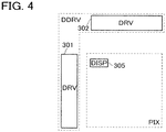
- FIG 4 is a diagram for explaining the display device in this embodiment.
- the display device illustrated in FIG 4 includes a display driving portion DDRV and a pixel portion PIX.
- the display driving portion DDRV controls display operation in the display device.
- the pixel portion PIX performs the display operation.
- the display device illustrated in FIG 4 includes a driver circuit (also referred to as DRV) 301, a driver circuit 302, and a plurality of display circuits (also referred to as DISP) 305.
- the driver circuit 301 is provided for the display driving portion DDRV.
- the driver circuit 301 has a function of selecting the display circuit 305.
- the driver circuit 301 has a shift register, for example. In that case, the driver circuit 301 can output a plurality of pulse signals from the shift register, and thus can output a signal for selecting the display circuit 305. Alternatively, the driver circuit 301 may have a plurality of shift registers. In that case, the driver circuit 301 can output a plurality of pulse signals from each of the plurality of shift registers, and thus can output a plurality of signals for controlling the display circuit 305.
- the driver circuit 302 is provided for the display driving portion DDRV.
- An image signal is input to the driver circuit 302.
- the driver circuit 302 has a function of generating a plurality of display data signals that is a voltage signal on the basis of the input image signal and outputting the plurality of generated display data signals.
- the driver circuit 302 includes a plurality of transistors, for example.
- the transistor has two terminals and a current control terminal that controls current flowing between the two terminals with an applied voltage.
- a current control terminal that controls current flowing between the two terminals with an applied voltage.
- terminals between which current flows and the current is controlled are also referred to as current terminals.
- Two current terminals are also referred to as a first current terminal and a second current terminal.
- a field-effect transistor can be used as a transistor, for example.
- a first current terminal is one of a source and a drain
- a second current terminal is the other of the source and the drain
- a current control terminal is a gate.
- the driver circuit 302 can output data of video signals as a plurality of display data signals by selectively turning on or off a plurality of transistors.
- the plurality of transistors can be controlled by inputting a control signal that is a pulse signal to their gates.
- the plurality of display circuits 305 are provided in the pixel portion PIX in rows and columns. Any one of a plurality of display data signals is input to each of the plurality of display circuits 305. Note that one pixel is formed using one or more display circuits 305.
- a full-color image in the pixel portion by providing a display circuit emitting red light, a display circuit emitting green light, and a display circuit emitting blue light and by making these display circuits emit light.
- one or more display circuits emitting light of one or more of the following colors: cyan, magenta, and yellow may be provided.
- a colored layer that transmits light with a particular wavelength of light emitted from a light-emitting element are provided in a display circuit, thereby achieving the emission of light of the particular color.
- This structure enables a full-color image to be displayed without forming a plurality of light emitting elements emitting light of different colors, thereby facilitating the manufacturing process, enhancing yield, and improving the quality and reliability of the light emitting elements.
- FIG. 5A is a circuit diagram illustrating the configuration example of the display circuit in this embodiment.
- the display circuit illustrated in FIG. 5A includes a transistor 331, a transistor 332, a light-emitting element (also referred to as LEE) 333, and a capacitor 335.
- the transistor 331 and the transistor 332 are field-effect transistors.
- the capacitor includes a first capacitor electrode, a second capacitor electrode, and a dielectric layer overlapping with the first capacitor electrode and the second capacitor electrode.
- the capacitor accumulates charge in accordance with a voltage applied between the first capacitor electrode and the second capacitor electrode.
- a display data signal (also referred to as a signal DD) is input to one of a source and a drain of the transistor 331.
- a display selection signal (also referred to as a signal DSEL) is input to a gate of the transistor 331.
- a voltage Vb is input to one of a source and a drain of the transistor 332.
- a gate of the transistor 332 is electrically connected to the other of the source and the drain of the transistor 331.
- a first electrode of the light-emitting element 333 is electrically connected to the other of the source and the drain of the transistor 332.
- a voltage Va is input to a second electrode of the light-emitting element 333.
- the voltage Vc is input to a first capacitor electrode of the capacitor 335.
- a second capacitor electrode of the capacitor 335 is electrically connected to the gate of the transistor 332.
- one of the voltage Va and the voltage Vb is a high power supply voltage Vdd, and the other is a low power supply voltage Vss.
- the absolute value of a difference between the voltage Va and the voltage Vb is preferably larger than at least the absolute value of the threshold voltage of the transistor 332.
- the voltage Va and the voltage Vb may interchange depending, for example, on the conductivity type of the transistor.
- the voltage Vc is set as appropriate.
- the transistor 331 is a signal-input selection transistor. Note that a signal-input selection signal is input from the driver circuit 301 illustrated in FIG. 4 .
- the transistor 332 is a driving transistor for controlling the amount of current flowing to the light-emitting element 333.
- the capacitor 335 is a storage capacitor holding charge, the amount of which is determined by a display data signal. Note that the capacitor 335 is not necessarily provided.
- each of the transistors 331 and 332 can be, for example, a transistor having a semiconductor layer containing a semiconductor that belongs to Group 14 in the periodic table (e.g., silicon) or an oxide semiconductor layer in which a channel is formed.
- the transistor including the oxide semiconductor layer has an off-state current lower than that of a conventional transistor including a semiconductor layer (e.g., a silicon layer).
- the oxide semiconductor layer has a wider band gap than silicon and is an intrinsic (i-type) or substantially intrinsic semiconductor layer.
- the off-state current per micrometer of channel width of the transistor having an oxide semiconductor layer is lower than or equal to 10 aA (1 ⁇ 10 -17 A), preferably lower than or equal to 1 aA (1 ⁇ 10 -18 A), more preferably lower than or equal to 10 zA (1 ⁇ 10 -20 A), more preferably lower than or equal to 1 zA (1 ⁇ 10 -21 A), more preferably lower than or equal to 100 yA (1 ⁇ 10 -22 A).
- FIG. 5B is a timing diagram for explaining the example of the method for driving the display circuit illustrated in FIG 5A , and illustrates the states of a signal DD, a signal DSEL, and the transistor 331.
- the signal DD is input to the display circuit, so that the voltage of the gate of the transistor 332 and the voltage of the second capacitor electrode of the capacitor 335 each become the same as the voltage of the signal DD (e.g., a voltage D11 here).
- the voltage of the first electrode of the light emitting element 333 depends on the voltage of the signal DD and the luminance of the light emitting element 333 becomes a value determined by the voltage Va and the voltage of the first electrode set in accordance with the signal DD.
- the transistor 331 switches to the off state (also called the state OFF).
- the display circuit has a circuit configuration illustrated in FIG 5A .
- a display device in this embodiment includes a first substrate (also referred to as an active matrix substrate) where a semiconductor element such as a transistor is provided, a second substrate, and a light-emitting element provided between the first substrate and the second substrate.
- a first substrate also referred to as an active matrix substrate
- a semiconductor element such as a transistor
- FIGS. 6A and 6B illustrate the structural example of the active matrix substrate in the display device in this embodiment.
- FIG. 6A is a schematic plan view
- FIG. 6B is a schematic cross-sectional view taken along line A-B in FIG 6A .
- the components illustrated in FIGS. 6A and 6B include those having sizes different from the actual sizes.
- part of a cross section taken along line A-B in FIG 6A is omitted in FIG. 6B .
- the active matrix substrate illustrated in FIGS. 6A and 6B includes a substrate 500, an insulating layer 501, semiconductor layers 511a and 511b, an insulating layer 513, conductive layers 514a to 514c, an insulating layer 515, and conductive layers 516a to 516d.
- the semiconductor layers 511a and 511b are each provided over the substrate 500 with the insulating layer 501 provided therebetween.
- the semiconductor layer 511a includes impurity regions 512a to 512d containing an impurity element imparting a p-type conductivity or an n-type conductivity.
- the semiconductor layer 511a functions as a layer in which the channel of a signal-input-selection transistor in the display circuit is formed (also referred to as a channel formation layer) and as the second capacitor electrode of the storage capacitor in the display circuit.
- a channel formation region of a signal-input selection transistor in the display circuit is provided between the impurity region 512a and the impurity region 512b and between the impurity region 512b and the impurity region 512c.
- the semiconductor layer 511b includes an impurity region 512e and an impurity region 512f containing an impurity element imparting a p-type conductivity or an n-type conductivity.
- the semiconductor layer 511b functions as a channel formation layer of a driving transistor of the display circuit.
- a channel formation region of the driving transistor in the display circuit is provided between the impurity region 512e and the impurity region 512f.
- the insulating layer 513 is provided over the semiconductor layers 511a and 511b.
- the insulating layer 513 functions as gate insulating layers of the signal-input selection transistor and the driving transistor in the display circuit, and a dielectric layer of a storage capacitor in the display circuit.
- the conductive layer 514a overlaps with part of the semiconductor layer 511a with the insulating layer 513 provided therebetween. Note that a region of the semiconductor layer 511a which overlaps with the conductive layer 514a is the channel formation region of the signal-input-selection transistor in the display circuit.
- the conductive layer 514a functions as the gate of the signal-input-selection transistor in the display circuit. Note that in FIGS. 6A and 6B , the conductive layer 514a overlaps with part of the semiconductor layer 511a at a plurality of portions.
- the conductive layer 514a does not necessarily overlap with part of the semiconductor layer 511a at a plurality of portions, but the switching characteristics of the signal-input-selection transistor in the display circuit can be improved when the conductive layer 514a overlaps with part of the semiconductor layer 511a at a plurality of portions.
- a region of the semiconductor layer 511a which overlaps with the conductive layer 514a may contain an impurity element imparting p-type or n-type conductivity, the concentration of which is lower than that of the impurity element in the impurity regions 512a to 512d provided in the semiconductor layer 511a.
- the conductive layer 514b overlaps over part of the semiconductor layer 511a with the insulating layer 513 provided therebetween.
- the conductive layer 514b functions as a first capacitor electrode of a storage capacitor in the display circuit.
- a region of the semiconductor layer 511a which overlaps with the conductive layer 514a may contain an impurity element imparting a p-type or n-type conductivity, the concentration of which is lower than that of the impurity element in the impurity regions 512a to 512d.
- the conductive layer 514b functions as the first capacitor electrode of the storage capacitor and a capacitor line in the display circuit.
- the conductive layer 514c overlaps with part of the semiconductor layer 511b with the insulating layer 513 provided therebetween.
- the conductive layer 514c functions as the gate of the driving transistor in the display circuit.
- the insulating layer 515 is provided over the insulating layer 513 with the conductive layers 514a to 514c provided therebetween.
- the conductive layer 516a is electrically connected to the impurity region 512a through a first opening formed in the insulating layer 513 and the insulating layer 515.
- the conductive layer 516a functions as a wiring to which one of the source and the drain of the signal-input-selection transistor in the display circuit and a wiring to which a display data signal is input.
- the conductive layer 516b is electrically connected to the impurity region 512d through a second opening formed in the insulating layer 513 and the insulating layer 515 and to the conductive layer 514c through a third opening formed in the insulating layer 515.
- the conductive layer 516b functions as the other of the source and the drain of the signal-input-selection transistor in the display circuit.
- the conductive layer 516c is electrically connected to the impurity region 512e through a fourth opening formed in the insulating layer 513 and the insulating layer 515.
- the conductive layer 516c functions as one of the source and the drain of the driving transistor in the display circuit and a power supply line to which the voltage Vb is input.
- the conductive layer 516d is electrically connected to the impurity region 512f through a fifth opening formed in the insulating layer 513 and the insulating layer 515.
- the conductive layer 516d functions as the other of the source and the drain of the driving transistor in the display circuit.
- FIG 7 is a schematic cross-sectional view illustrating a structural example of the display device of this embodiment.
- a light-emitting element in the display device emits light in the direction of the top surface of the display device; however, this embodiment is not limited thereto.
- the display device of this embodiment may emit light in the direction of the bottom surface.
- the display device illustrated in FIG 7 includes an insulating layer 517, a conductive layer 518, a conductive layer 519, a conductive layer 520, an insulating layer 521, a light-emitting layer 522, a conductive layer 523, a substrate 524, a colored layer 525, an insulating layer 526, and an insulating layer 527 in addition to the active matrix substrate illustrated in FIGS. 6A and 6B .
- the insulating layer 517 is provided over the insulating layer 515 with the conductive layers 516a to 516d provided therebetween.
- the conductive layer 518 is provided over the insulating layer 517 of the display circuit and is electrically connected to the conductive layer 516d through a sixth opening in the insulating layer 517.
- the conductive layer 519 is provided over the conductive layer 518.
- the conductive layer 519 is electrically connected to the conductive layer 518.
- the conductive layer 520 is provided over the conductive layer 519.
- the conductive layer 520 is electrically connected to the conductive layer 519.
- the conductive layers 518 to 520 correspond to an electrode layer of the light-emitting element described in the above embodiment. Note that the conductive layers 518 to 520 function as a first electrode of the light-emitting element of the display circuit.
- the insulating layer 521 is provided over the conductive layer 518.
- the light-emitting layer 522 is provided over the insulating layer 521 and is electrically connected to the conductive layer 518 through a seventh opening formed in the insulating layer 521.
- the light-emitting layer 522 functions as a light-emitting layer of the light-emitting element in the display circuit.
- the conductive layer 523 is provided over and is electrically connected to the light-emitting layer 522.
- the conductive layer 523 corresponds to an electrode layer of the light-emitting element described in the above embodiment.
- the conductive layer 523 functions as a second electrode of the light-emitting element in the display circuit.
- the colored layer 525 is provided over one surface of the substrate 524 and transmits light with a particular wavelength of light emitted from the light-emitting layer 522.
- the insulating layer 526 is provided over the one surface of the substrate 524 with the colored layer 525 provided therebetween.
- the insulating layer 527 is provided between the insulating layer 526 and the conductive layer 523.
- a glass substrate or a plastic substrate can be used for the substrates 500 and 524.
- a silicon oxide layer, a silicon nitride layer, a silicon oxynitride layer, a silicon nitride oxide layer, an aluminum oxide layer, an aluminum nitride layer, an aluminum oxynitride layer, an aluminum nitride oxide layer, or a hafnium oxide layer can be used, for example.
- An oxide insulating layer such as a silicon oxide layer or a silicon oxynitride layer is preferably used as the insulating layer 501.
- the oxide insulating layer may contain halogen.
- the insulating layer 501 can be a stack of the aforementioned materials which can be used for the insulating layer 501.
- the insulating layer 501 is not necessarily provided.
- the semiconductor layer 511 a and 511b can be, for example, a layer containing an amorphous semiconductor, a microcrystalline semiconductor, a polycrystalline semiconductor, or a single crystal semiconductor.
- a semiconductor layer including a semiconductor belonging to Group 14 of the periodic table e.g., silicon can be used as the semiconductor layers 511a and 511b.
- the insulating layer 513 can be a layer of a material which can be used for the insulating layer 501 or a layer of a resin material.
- the insulating layer 513 can be a stack of materials which can be used for the insulating layer 513.
- a layer formed using a metal such as molybdenum, titanium, chromium, tantalum, magnesium, silver, tungsten, aluminum, copper, neodymium, or scandium can be used for the conductive layers 514a to 514c.
- each of the conductive layers 514a to 514c can be, for example, a layer containing a conductive metal oxide.
- the conductive metal oxide can be a metal oxide such as indium oxide (In 2 O3).
- the conductive layers 514a to 514c can also be a stack of the aforementioned materials which can be used for the conductive layers 514a to 514c.
- the conductive layers 514a to 514c can be a stack of a tantalum nitride layer and a tungsten layer, for example.
- the insulating layer 515 can be a layer of a material which can be used for the insulating layer 501 or the insulating layer 513.
- the insulating layer 515 can be a stack of the aforementioned materials which can be used for the insulating layer 501.
- the insulating layer 515 can be a stack of a silicon nitride oxide layer and a silicon oxynitride layer.
- Each of the conductive layers 516a to 516d can be a layer of a material which can be used for the conductive layer 514a to 514c, for example.
- Each of the conductive layers 516a to 516d can be a stack of materials which can be used for the conductive layers 516a to 516d.
- each of the conductive layers 516a to 516d can be a stack of a titanium layer, an aluminum layer, and a titanium layer. Note that side surfaces of each of the conductive layers 516a to 516d may be tapered.
- the insulating layer 517 can be a layer of a material which can be used for the insulating layer 513 or the insulating layer 513, for example.
- the insulating layer 517 can be a stack of materials which can be used for the insulating layer 517.
- the conductive layer 518 can be a layer of a material which can be used for the conductive layer 111 illustrated in FIG. 1B , for example.
- the conductive layer 519 can be a layer of a material which can be used for the conductive layer 112 illustrated in FIG 1B , for example.
- the conductive layer 520 can be a layer of a material which can be used for the conductive layer 113 illustrated in FIG 1B , for example.
- the insulating layer 521 can be an organic insulating layer or an inorganic insulating layer, for example. Note that the insulating layer 521 is also referred to as a partition.
- the light-emitting layer 522 can be a layer of a material (e.g., a light-emitting layer emitting white light) which can be used for the light-emitting layer described in the above embodiment.
- a material e.g., a light-emitting layer emitting white light
- the conductive layer 523 can be a layer of a light-transmitting material selected from the materials which can be used for the conductive layers 514a to 514.
- the conductive layer 523 can be a stack of materials which can be used for the conductive layer 523.
- the colored layer 525 can be a layer which includes dye or pigment, for example, and which transmits light with the wavelength range of red, light with the wavelength range of green, and light with the wavelength range of blue.
- the colored layer 525 can be a layer which includes dye or pigment, for example, and which transmits light with the wavelength range of cyan, magenta, or yellow.
- the colored layer 525 is formed by the photolithography method, the printing method, the inkjet method, the printing method, the electrodeposition method, the electrophotographic method, or the like. By using the inkjet method, the colored layer can be manufactured at room temperature, manufactured at a low vacuum, or formed over a large substrate. Since the colored layer can be manufactured without a resist mask, manufacturing cost and the number of steps can be reduced.
- the insulating layer 526 can be a layer of a material which can be used for the insulating layer 501 or the insulating layer 513.
- the insulating layer 526 can be a stack of materials which can be used for the insulating layer 526. Note that the insulating layer 526 is not necessarily provided, but providing the insulating layer 526 can suppress the entry of an impurity from the colored layer 525 to the light emitting element.
- the insulating layer 527 can be a layer of a material which can be used for the insulating layer 501 or a layer of a resin material.
- the insulating layer 527 can be a stack of materials which can be used for the insulating layer 527.
- an example of the display device in this embodiment includes the signal-input selection transistor (first field-effect transistor) in which a display data signal is input to one of a source and a drain, the driving transistor (second field-effect transistor) whose gate is electrically connected to the other of the source and the drain of the first field-effect transistor, and a light-emitting element whose first electrode is electrically connected to one of a source and a drain of the second field-effect transistor and which has a structure described in the above embodiment.
- first field-effect transistor the signal-input selection transistor
- driving transistor second field-effect transistor
- a light-emitting element whose first electrode is electrically connected to one of a source and a drain of the second field-effect transistor and which has a structure described in the above embodiment.
- An example of the display device in this embodiment includes a light-emitting element emitting white light and a colored layer which transmits light with a particular wavelength of light emitted from the light emitting element.
- This structure enables a full-color image to be displayed without forming plural kinds of light emitting elements emitting light of different colors, thereby facilitating the manufacturing process and enhancing yield.
- a display element can be formed without a metal mask, and therefore, a manufacturing process can be simple. Further, contrast of an image can be improved. Further, the quality and reliability of a light-emitting element can be improved.
- a light-emitting element has a structure in which light is extracted through a substrate provided with no element such as a transistor, so that a region above a region provided with the element can be used as a light-emitting region; therefore, an aperture ratio can be improved.
- a driver circuit may be provided over the same substrate as the display circuit.
- the transistor in the circuit such as a driver circuit may have the same structure as the transistor in the display circuit.
- a circuit such as the driver circuit is provided over the same substrate as the display circuit, so that the number of connection wirings of the display circuit and the driver circuit can be reduced.
- FIGS. 8A to 8D are schematic views each illustrating a structural example of the electronic device of this embodiment.
- An electronic device in FIG. 8A is an example of a mobile information terminal.
- the mobile information terminal in FIG 8A includes a housing 1001a and a display portion 1002a provided in the housing 1001a.
- a side surface 1003a of the housing 1001a may be provided with a connection terminal for connecting the mobile information terminal to an external device and/or a button used to operate the mobile information terminal in FIG 8A .
- the mobile information terminal in FIG 8A includes a CPU, a main memory, an interface transmitting/receiving a signal traveling between the external device and each of the CPU and the main memory, and an antenna transmitting/receiving a signal to/from the external device, in the housing 1001a.
- a CPU central processing unit
- main memory main memory
- an antenna transmitting/receiving a signal to/from the external device, in the housing 1001a.
- the housing 1001a one or plural integrated circuits having a specific function may be provided.
- the mobile information terminal in FIG. 8A functions, for example, as one or more devices selected from a telephone, an electronic book, a personal computer, and a game machine.
- An electronic device in FIG. 8B is an example of a folding mobile information terminal.
- the mobile information terminal in FIG. 8B includes a housing 1001b, a display portion 1002b provided in the housing 1001b, a housing 1004, a display portion 1005 provided in the housing 1004, and a hinge 1006 for connecting the housing 1001b and the housing 1004.
- the housing 1001b can be stacked on the housing 1004 by moving the housing 1001b or the housing 1004 with the hinge 1006.
- a side surface 1003b of the housing 1001b or a side surface 1007 of the housing 1004 may be provided with a connection terminal for connecting the mobile information terminal to an external device and/or a button used to operate the mobile information terminal in FIG. 8B .
- the display portion 1002b and the display portion 1005 may display different images or one image. Note that the display portion 1005 is not necessarily provided: a keyboard which is an input device may be provided instead of the display portion 1005.
- a CPU In the housing 1001b or the housing 1004 of the portable information terminal illustrated in FIG 8B , a CPU, a main memory, and an interface transmitting/receiving a signal traveling between the external device and the CPU and the main memory are provided. Note that in the housing 1001b or the housing 1004, one or plural integrated circuits having a specific function may be provided.
- the mobile information terminal in FIG. 8B may include an antenna transmitting/receiving a signal to/from the external device.
- the mobile information terminal in FIG. 8B functions, for example, as one or more devices selected from a telephone, an electronic book, a personal computer, and a game machine.
- the electronic device in FIG. 8C is an example of a stationary information terminal.
- the stationary information terminal in FIG. 8C includes a housing 1001c and a display portion 1002c provided in the housing 1001c.
- the display portion 1002c can be provided on a deck portion 1008 of the housing 1001c.
- the stationary information terminal in FIG. 8C includes a CPU. a main memory, and an interface transmitting/receiving a signal traveling between the external device and each of the CPU and the main memory, in the housing 1001c. Note that in the housing 1001c, one or plural integrated circuits having a specific function may be provided. In addition, the stationary information terminal in FIG 8C may include an antenna transmitting/receiving a signal to/from the external device.
- a side surface 1003c of the housing 1001c in the stationary information terminal in FIG. 8C may be provided with one or more parts selected from a ticket ejection portion that ejects a ticket or the like, a coin slot, and a bill slot.
- the stationary information terminal in FIG 8C functions, for examples, as an automated teller machine, an information communication terminal for ticketing or the like (also referred to as a multi-media station), or a game machine.
- FIG. 8D illustrates an example of a stationary information terminal.
- the stationary information terminal in FIG 8D includes a housing 1001d and a display portion 1002d provided in the housing 1001d. Note that a support for supporting the housing 1001d may also be provided.
- a side surface 1003d of the housing 1001d may be provided with a connection terminal for connecting the mobile information terminal to an external device and/or a button used to operate the mobile information terminal in FIG. 8D .
- the stationary information terminal illustrated in FIG 8D may also include, in the housing 1001d, a CPU, a main memory, and an interface transmitting/receiving a signal traveling between the external device and the CPU and the main memory. Further, in the housing 1001d, one or plural integrated circuits having a specific function may be provided. In addition, the stationary information terminal in FIG. 8D may include an antenna transmitting/receiving a signal to/from the external device.
- the stationary information terminal illustrated in FIG 8D functions, for example, as a digital photo frame, a display monitor, or a television set.
- the display device described in the above embodiments is used for a display portion of an electronic device, and for example, used for the display portions 1002a to 1002d illustrated in FIGS. 8A to 8D . Further, the display device of the above embodiment may be used for the display portion 1005 illustrated in FIG. 8B .
- a light source part of the electronic device may be provided instead of the display device in the above embodiment, and a lighting device including the light-emitting element in the above embodiment may be provided for the light source part.
- the display device in the above embodiment is used for a display portion; therefore, power consumption can be reduced and reliability can be improved.
- the housing may be provided with one or more of a photoelectric conversion portion which generates current in accordance with incident illuminance and an operation portion for operating the display device.
- a photoelectric transducer for example, eliminates necessity of an external power source, allowing the above electronic device to be used for a long period of time even in a place without an external power source.
- FIGS. 9A to 9D are schematic views of the examples of the lighting devices in this embodiment.
- a lighting device 1201a illustrated in FIG 9A is an example of a lighting device which can be attached to a ceiling of a room.
- FIG 9B illustrates a structural example the lighting device illustrated in FIG. 9A .
- the lighting device illustrated in FIG. 9B includes a base 1211 attached to a ceiling 1210; a stack of an electrode layer 1212, and a light-emitting layer 1213, an electrode layer 1214, which is provided over the base 1211; a lens 1215 provided over the electrode layer 1214; sealant 1216; and a base 1217 bonded to the base 1211 with the sealant 1216.
- the base 1211 can be a substrate of aluminum oxide, duralumin, or magnesium oxide, for example. By using the substrate, heat can be easily released through the base 1211.
- the electrode layer 1212 can be a layer of a material which can be used for the first electrode layer of the light-emitting element in the above embodiment, for example.
- the light-emitting layer 1213 can be a layer of a material which can be used for the light-emitting layer of the light-emitting element in the above embodiment, for example.
- the electrode layer 1214 can be a layer of a material which can be used for the second electrode layer of the light-emitting element in the above embodiment, for example.
- the lens 1215 is formed of, for example, a material such as a resin.
- the lens 1215 has unevenness at the top surface, and preferably has hemispherical projections. With the lens 1215, light extraction efficiency can be enhanced.
- the base 1217 can be a glass substrate, for example.
- the lighting device 1201a illustrated in FIG. 9A includes a light-emitting portion provided with the light-emitting element in the above embodiment.
- the light-emitting portion may include desiccant.
- the lighting device 1201a may be provided with a control circuit configured to control light emission of the light-emitting element.
- the lighting device illustrated in FIG. 9A is manufactured using the light-emitting element in any of the above embodiments, whereby the area of the lighting device can be easily increased.
- a lighting device 1201b illustrated in FIG 9C is an example of a lighting device which can be attached to a sidewall of a room.
- the lighting device 1201b includes the light-emitting element or the lighting device in the above embodiment, and a control circuit configured to control light emission of the light-emitting element.
- the lighting device illustrated in FIG. 9C is manufactured using the light-emitting element in the above embodiment to the light-emitting portion, whereby the area of the lighting device can be easily increased.
- a light-transmitting glass substrate is used as a substrate of the lighting device 1201b, whereby the lighting device 1201b can be used as window glass.
- the lighting device illustrated in FIG. 9D is an example of a lighting device which can change the position of a light-emitting portion.
- the lighting device illustrated in FIG. 9D includes a body 1221 and the light-emitting portion 1222.
- the light-emitting portion 1222 can include the light-emitting element in the above embodiment.
- the body 1221 may be flexible.
- a light-emitting element provided over a plastic substrate is used for the light-emitting portion, whereby the position of the light-emitting portion 1222 can be adjusted by bending the body back-and-forth.
- the lighting devices can be manufactured by providing the light-emitting element in any of the above embodiments in the light-emitting portions.
- a lighting device is manufactured by using the light-emitting element in any of the above embodiments in a light-emitting portion, whereby the power consumption of the lighting device can be reduced.
- a lighting device is manufactured by using the light-emitting element in any of the above embodiments, whereby the light emission area of the lighting device can be easily increased.
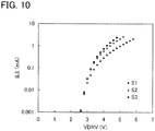
- light-emitting elements of a sample 1 (S1), a sample 2 (S2), and a sample 3 (S3) were manufactured.
- the light-emitting elements of the samples 1 to 3 each included a lower electrode (also referred to as ED(DOWN)), a hole-injection layer (HIL), a hole-transport layer (HTL), an electroluminescence layer (ELL), an electron-transport layer (ETL), an electron-injection layer (EIL), and an upper electrode (also referred to as ED(UP)).
- a lower electrode also referred to as ED(DOWN)
- HIL hole-injection layer
- HTL hole-transport layer
- ELL electroluminescence layer
- ETL electron-transport layer
- EIL electron-injection layer
- Table 1 shows a specific structure (material (MT), thickness (TN), and the like) of each light-emitting element.
- the lower electrode (ED(DOWN)) was formed over a glass substrate.
- an alloy layer of aluminum and titanium (A1-Ti) was formed over the glass substrate by sputtering using a target in which aluminum content was 99 wt% and titanium content was 1 wt%.
- a titanium layer was formed by sputtering using a titanium target. Heat treatment was performed at 250 °C for 1 hour.
- an indium oxide-tin oxide layer containing silicon oxide was formed by sputtering using a target in which In 2 O 3 content was 85 wt%, SnO 2 content was 10 wt%, and SiO 2 content was 5 wt%.
- the lower electrode was formed.
- a layer of NPB was formed by an evaporation method, so that the hole-transport layer was formed.
- a layer of Alq was formed by an evaporation method and a layer of Bphen was formed by an evaporation method, so that the electron-transport layer was formed.
- a layer of lithium fluoride was formed by an evaporation method, so that the electron-injection layer was formed.
- the above is a manufacturing method of the light-emitting elements of the samples 1 to 3.
- FIG 10 shows a result of current (ILE)-voltage (VDRV) characteristics of the samples 1 (S1) to 3 (S3).
- the current amount of the samples 2 and 3 for which conductive layers (MOL) including a metal oxide were provided is large. Therefore, it can be found that voltage with respect to the predetermined current amount, that is, driving voltage can be lower by using a conductive layer containing a metal oxide.
Landscapes
- Physics & Mathematics (AREA)
- Optics & Photonics (AREA)
- Electroluminescent Light Sources (AREA)
- Devices For Indicating Variable Information By Combining Individual Elements (AREA)
Applications Claiming Priority (1)
| Application Number | Priority Date | Filing Date | Title |
|---|---|---|---|
| JP2011027958 | 2011-02-11 |
Publications (2)
| Publication Number | Publication Date |
|---|---|
| EP2487733A1 EP2487733A1 (en) | 2012-08-15 |
| EP2487733B1 true EP2487733B1 (en) | 2020-01-22 |
Family
ID=45655612
Family Applications (1)
| Application Number | Title | Priority Date | Filing Date |
|---|---|---|---|
| EP12155048.7A Active EP2487733B1 (en) | 2011-02-11 | 2012-02-13 | Light-emitting element, display device, lighting device, and method for manufacturing the same |
Country Status (6)
| Country | Link |
|---|---|
| US (1) | US9564609B2 (enExample) |
| EP (1) | EP2487733B1 (enExample) |
| JP (1) | JP5969216B2 (enExample) |
| KR (1) | KR101945315B1 (enExample) |
| CN (1) | CN102637830B (enExample) |
| TW (1) | TWI575774B (enExample) |
Families Citing this family (28)
| Publication number | Priority date | Publication date | Assignee | Title |
|---|---|---|---|---|
| US9083000B2 (en) | 2011-04-29 | 2015-07-14 | Semiconductor Energy Laboratory Co., Ltd. | Light-emitting element, light-emitting device, and lighting device |
| KR101917752B1 (ko) | 2011-05-11 | 2018-11-13 | 가부시키가이샤 한도오따이 에네루기 켄큐쇼 | 발광 소자, 발광 모듈, 발광 패널, 발광 장치 |
| US9721998B2 (en) | 2011-11-04 | 2017-08-01 | Semiconductor Energy Laboratory Co., Ltd. | Display device and driving method thereof |
| DE102013112602B4 (de) | 2012-12-18 | 2020-11-12 | Lg Display Co., Ltd. | Weiße organische Lichtemissionsvorrichtung |
| JP6099420B2 (ja) | 2013-02-08 | 2017-03-22 | 株式会社半導体エネルギー研究所 | 発光装置 |
| JP6615253B2 (ja) * | 2013-04-30 | 2019-12-04 | キヤノン株式会社 | 有機発光素子 |
| JP2015049947A (ja) * | 2013-08-29 | 2015-03-16 | 株式会社ジャパンディスプレイ | 有機エレクトロルミネッセンス表示装置 |
| JP6488082B2 (ja) * | 2013-12-02 | 2019-03-20 | 株式会社半導体エネルギー研究所 | 発光装置、電子機器、および照明装置 |
| TWI776722B (zh) | 2014-05-15 | 2022-09-01 | 日商半導體能源研究所股份有限公司 | 發光元件、發光裝置、電子裝置以及照明設備 |
| US9874775B2 (en) | 2014-05-28 | 2018-01-23 | Semiconductor Energy Laboratory Co., Ltd. | Liquid crystal display device and electronic device |
| KR102377360B1 (ko) | 2014-08-08 | 2022-03-21 | 가부시키가이샤 한도오따이 에네루기 켄큐쇼 | 발광 소자, 발광 장치, 조명 장치, 표시 장치, 디스플레이 패널, 전자 기기 |
| US9343691B2 (en) | 2014-08-08 | 2016-05-17 | Semiconductor Energy Laboratory Co., Ltd. | Light-emitting element, light-emitting device, electronic device, and lighting device |
| KR20160028580A (ko) * | 2014-09-03 | 2016-03-14 | 삼성디스플레이 주식회사 | 컬러 변환층을 포함하는 표시장치 |
| WO2016063169A1 (en) | 2014-10-23 | 2016-04-28 | Semiconductor Energy Laboratory Co., Ltd. | Light-emitting element |
| US10680017B2 (en) | 2014-11-07 | 2020-06-09 | Semiconductor Energy Laboratory Co., Ltd. | Light-emitting element including EL layer, electrode which has high reflectance and a high work function, display device, electronic device, and lighting device |
| KR102294413B1 (ko) * | 2014-11-18 | 2021-08-27 | 삼성디스플레이 주식회사 | 유기발광 표시장치 |
| CN104393023B (zh) * | 2014-12-01 | 2018-01-26 | 京东方科技集团股份有限公司 | 一种阵列基板及其制作方法、显示装置 |
| KR102543330B1 (ko) | 2015-02-25 | 2023-06-14 | 가부시키가이샤 한도오따이 에네루기 켄큐쇼 | 발광 소자, 표시 소자, 표시 장치, 전자 기기, 및 조명 장치 |
| JP7016633B2 (ja) * | 2016-10-28 | 2022-02-07 | キヤノン株式会社 | 複数の有機el素子を有する白色発光装置 |
| US11462711B2 (en) | 2017-06-26 | 2022-10-04 | Samsung Display Co., Ltd. | Light-emitting device and method of fabricating display panel therewith |
| KR20190001629A (ko) * | 2017-06-26 | 2019-01-07 | 삼성디스플레이 주식회사 | 발광소자 및 표시패널의 제조방법 |
| CN112970130B (zh) * | 2018-10-30 | 2024-02-09 | 夏普株式会社 | 发光元件、发光元件的制造方法 |
| US12274114B2 (en) * | 2019-09-06 | 2025-04-08 | Sharp Kabushiki Kaisha | Display device including metal oxide nanoparticles for uniform and efficient lighting and method for producing same |
| KR102806843B1 (ko) * | 2020-07-01 | 2025-05-12 | 삼성전자주식회사 | 발광 소자 및 이를 포함하는 표시 장치 |
| JP7724805B2 (ja) * | 2021-01-28 | 2025-08-18 | 株式会社半導体エネルギー研究所 | 表示装置 |
| KR102950780B1 (ko) * | 2021-06-23 | 2026-04-09 | 삼성디스플레이 주식회사 | 표시 장치 및 그 제조방법 |
| KR20230061287A (ko) * | 2021-10-28 | 2023-05-08 | 삼성전자주식회사 | 전계발광소자 및 그 제조방법과 이를 포함하는 표시 장치 |
| CN115915827A (zh) * | 2022-10-08 | 2023-04-04 | 深圳市华星光电半导体显示技术有限公司 | 显示面板及其制作方法 |
Citations (2)
| Publication number | Priority date | Publication date | Assignee | Title |
|---|---|---|---|---|
| US20100123152A1 (en) * | 2008-11-19 | 2010-05-20 | Semiconductor Energy Laboratory Co., Ltd. | Light-Emitting Element, Light-Emitting Device, Electronic Device, and Lighting Device |
| US20100225227A1 (en) * | 2006-11-17 | 2010-09-09 | Svetoslav Tchakarov | Electrode for an organic light-emitting device, acid etching thereof and also organic light-emitting device incorporating it |
Family Cites Families (117)
| Publication number | Priority date | Publication date | Assignee | Title |
|---|---|---|---|---|
| JP2636341B2 (ja) | 1988-06-09 | 1997-07-30 | 日本電気株式会社 | 有機薄膜el素子 |
| JP2666428B2 (ja) | 1988-11-18 | 1997-10-22 | 日本電気株式会社 | 有機薄膜el素子 |
| JP2773297B2 (ja) | 1989-09-28 | 1998-07-09 | 日本電気株式会社 | 有機薄膜el素子 |
| JPH03190088A (ja) | 1989-12-20 | 1991-08-20 | Sanyo Electric Co Ltd | 有機el素子 |
| JP2926845B2 (ja) | 1990-03-23 | 1999-07-28 | 日本電気株式会社 | 有機薄膜el素子 |
| JPH04357694A (ja) | 1991-06-03 | 1992-12-10 | Denki Kagaku Kogyo Kk | 有機薄膜el素子 |
| JPH05182766A (ja) | 1991-12-26 | 1993-07-23 | Toyota Central Res & Dev Lab Inc | 薄膜el素子 |
| JPH06267658A (ja) | 1993-03-09 | 1994-09-22 | Mitsubishi Kasei Corp | 有機el素子 |
| JP2797883B2 (ja) | 1993-03-18 | 1998-09-17 | 株式会社日立製作所 | 多色発光素子とその基板 |
| JP3189480B2 (ja) | 1993-04-02 | 2001-07-16 | 富士電機株式会社 | 有機薄膜発光素子 |
| JPH07312289A (ja) | 1994-05-18 | 1995-11-28 | Mitsubishi Chem Corp | 有機電界発光素子 |
| JP2824411B2 (ja) | 1995-08-25 | 1998-11-11 | 株式会社豊田中央研究所 | 有機薄膜発光素子 |
| JPH10172762A (ja) | 1996-12-11 | 1998-06-26 | Sanyo Electric Co Ltd | エレクトロルミネッセンス素子を用いた表示装置の製造方法及び表示装置 |
| JPH10270171A (ja) | 1997-01-27 | 1998-10-09 | Junji Kido | 有機エレクトロルミネッセント素子 |
| US5989737A (en) | 1997-02-27 | 1999-11-23 | Xerox Corporation | Organic electroluminescent devices |
| JP3571171B2 (ja) | 1997-05-08 | 2004-09-29 | 出光興産株式会社 | 有機エレクトロルミネッセンス素子 |
| GB9803764D0 (en) | 1998-02-23 | 1998-04-15 | Cambridge Display Tech Ltd | Display devices |
| JPH11251067A (ja) | 1998-03-02 | 1999-09-17 | Junji Kido | 有機エレクトロルミネッセント素子 |
| JP3468089B2 (ja) | 1998-04-07 | 2003-11-17 | 松下電器産業株式会社 | 有機電界発光素子 |
| JPH11307264A (ja) | 1998-04-17 | 1999-11-05 | Matsushita Electric Ind Co Ltd | 有機電界発光素子 |
| JPH11307259A (ja) | 1998-04-23 | 1999-11-05 | Tdk Corp | 有機el素子 |
| US6486601B1 (en) | 1998-06-26 | 2002-11-26 | Idemitsu Kosan Co., Ltd. | Organic luminescence device with reduced leakage current |
| JP4198253B2 (ja) | 1999-02-02 | 2008-12-17 | 出光興産株式会社 | 有機エレクトロルミネッセンス素子およびその製造方法 |
| JP4420486B2 (ja) | 1999-04-30 | 2010-02-24 | 出光興産株式会社 | 有機エレクトロルミネッセンス素子およびその製造方法 |
| JP2000315581A (ja) | 1999-04-30 | 2000-11-14 | Idemitsu Kosan Co Ltd | 有機エレクトロルミネッセンス素子およびその製造方法 |
| JP5210473B2 (ja) * | 1999-06-21 | 2013-06-12 | 株式会社半導体エネルギー研究所 | 表示装置 |
| JP4666722B2 (ja) | 1999-06-28 | 2011-04-06 | 株式会社半導体エネルギー研究所 | El表示装置及び電子装置 |
| TW543206B (en) | 1999-06-28 | 2003-07-21 | Semiconductor Energy Lab | EL display device and electronic device |
| JP2001043980A (ja) | 1999-07-29 | 2001-02-16 | Sony Corp | 有機エレクトロルミネッセンス素子及び表示装置 |
| TW474114B (en) | 1999-09-29 | 2002-01-21 | Junji Kido | Organic electroluminescent device, organic electroluminescent device assembly and method of controlling the emission spectrum in the device |
| JP4824848B2 (ja) | 2000-02-29 | 2011-11-30 | 淳二 城戸 | 有機エレクトロルミネッセント素子、有機エレクトロルミネッセント素子群及びその発光スペクトルの特定方法 |
| TW480722B (en) | 1999-10-12 | 2002-03-21 | Semiconductor Energy Lab | Manufacturing method of electro-optical device |
| JP4780826B2 (ja) | 1999-10-12 | 2011-09-28 | 株式会社半導体エネルギー研究所 | 電気光学装置の作製方法 |
| TW511298B (en) | 1999-12-15 | 2002-11-21 | Semiconductor Energy Lab | EL display device |
| US20010053559A1 (en) | 2000-01-25 | 2001-12-20 | Semiconductor Energy Laboratory Co., Ltd. | Method of fabricating display device |
| US6559594B2 (en) | 2000-02-03 | 2003-05-06 | Semiconductor Energy Laboratory Co., Ltd. | Light-emitting device |
| KR20010085420A (ko) | 2000-02-23 | 2001-09-07 | 기타지마 요시토시 | 전계발광소자와 그 제조방법 |
| TW521303B (en) | 2000-02-28 | 2003-02-21 | Semiconductor Energy Lab | Electronic device |
| US6608449B2 (en) | 2000-05-08 | 2003-08-19 | Semiconductor Energy Laboratory Co., Ltd. | Luminescent apparatus and method of manufacturing the same |
| US6692845B2 (en) | 2000-05-12 | 2004-02-17 | Semiconductor Energy Laboratory Co., Ltd. | Light-emitting device |
| US6483236B1 (en) | 2000-05-24 | 2002-11-19 | Eastman Kodak Company | Low-voltage organic light-emitting device |
| US6489638B2 (en) | 2000-06-23 | 2002-12-03 | Semiconductor Energy Laboratory Co., Ltd. | Light emitting device |
| DE10058578C2 (de) | 2000-11-20 | 2002-11-28 | Univ Dresden Tech | Lichtemittierendes Bauelement mit organischen Schichten |
| SG118118A1 (en) | 2001-02-22 | 2006-01-27 | Semiconductor Energy Lab | Organic light emitting device and display using the same |
| JP3955744B2 (ja) | 2001-05-14 | 2007-08-08 | 淳二 城戸 | 有機薄膜素子の製造方法 |
| JP3773423B2 (ja) | 2001-06-11 | 2006-05-10 | Tdk株式会社 | 有機el素子 |
| US6788108B2 (en) * | 2001-07-30 | 2004-09-07 | Semiconductor Energy Laboratory Co., Ltd. | Semiconductor device |
| JP2003109775A (ja) | 2001-09-28 | 2003-04-11 | Sony Corp | 有機電界発光素子 |
| JP4149168B2 (ja) * | 2001-11-09 | 2008-09-10 | 株式会社半導体エネルギー研究所 | 発光装置 |
| JP3742054B2 (ja) | 2001-11-30 | 2006-02-01 | 株式会社半導体エネルギー研究所 | 表示装置 |
| US7141817B2 (en) | 2001-11-30 | 2006-11-28 | Semiconductor Energy Laboratory Co., Ltd. | Light emitting device |
| TWI258317B (en) | 2002-01-25 | 2006-07-11 | Semiconductor Energy Lab | A display device and method for manufacturing thereof |
| JP3933591B2 (ja) | 2002-03-26 | 2007-06-20 | 淳二 城戸 | 有機エレクトロルミネッセント素子 |
| JP4683825B2 (ja) * | 2002-04-24 | 2011-05-18 | 株式会社半導体エネルギー研究所 | 半導体装置およびその作製方法 |
| US7786496B2 (en) | 2002-04-24 | 2010-08-31 | Semiconductor Energy Laboratory Co., Ltd. | Semiconductor device and method of manufacturing same |
| US7158161B2 (en) | 2002-09-20 | 2007-01-02 | Matsushita Electric Industrial Co., Ltd. | Organic electroluminescence element and an exposure unit and image-forming apparatus both using the element |
| JP2004134395A (ja) | 2002-09-20 | 2004-04-30 | Matsushita Electric Ind Co Ltd | 有機エレクトロルミネッセンス素子およびそれを用いた露光装置ならびに画像形成装置 |
| JP2004178930A (ja) | 2002-11-26 | 2004-06-24 | Sony Corp | 発光素子およびこれを用いた表示装置 |
| JP4401657B2 (ja) * | 2003-01-10 | 2010-01-20 | 株式会社半導体エネルギー研究所 | 発光装置の製造方法 |
| US20040140758A1 (en) | 2003-01-17 | 2004-07-22 | Eastman Kodak Company | Organic light emitting device (OLED) display with improved light emission using a metallic anode |
| JP4624653B2 (ja) | 2003-05-20 | 2011-02-02 | 出光興産株式会社 | 有機エレクトロルミネッセンス素子及び表示装置 |
| US6909233B2 (en) * | 2003-06-11 | 2005-06-21 | Eastman Kodak Company | Stacked OLED display having improved efficiency |
| JP2005026121A (ja) | 2003-07-03 | 2005-01-27 | Fujitsu Ltd | 有機el素子及びその製造方法並びに有機elディスプレイ |
| JP4396163B2 (ja) | 2003-07-08 | 2010-01-13 | 株式会社デンソー | 有機el素子 |
| WO2005006460A1 (en) | 2003-07-09 | 2005-01-20 | Matsushita Electric Industrial Co., Ltd. | Organic electroluminescence element and an exposure unit and image-forming apparatus both using the element |
| KR100546662B1 (ko) | 2003-08-05 | 2006-01-26 | 엘지전자 주식회사 | 유기 el 소자 |
| KR100543005B1 (ko) * | 2003-09-18 | 2006-01-20 | 삼성에스디아이 주식회사 | 능동 매트릭스 유기전계발광표시장치 |
| TWI407830B (zh) | 2003-09-26 | 2013-09-01 | 半導體能源研究所股份有限公司 | 發光元件和其製法 |
| JP4683829B2 (ja) | 2003-10-17 | 2011-05-18 | 淳二 城戸 | 有機エレクトロルミネッセント素子及びその製造方法 |
| JP4476594B2 (ja) | 2003-10-17 | 2010-06-09 | 淳二 城戸 | 有機エレクトロルミネッセント素子 |
| TW200515836A (en) | 2003-10-22 | 2005-05-01 | Hannstar Display Corp | Organic electroluminescent element |
| JP4243237B2 (ja) | 2003-11-10 | 2009-03-25 | 淳二 城戸 | 有機素子、有機el素子、有機太陽電池、及び、有機fet構造、並びに、有機素子の製造方法 |
| JP4300176B2 (ja) | 2003-11-13 | 2009-07-22 | ローム株式会社 | 有機エレクトロルミネッセント素子 |
| US7374828B2 (en) | 2003-12-05 | 2008-05-20 | Eastman Kodak Company | Organic electroluminescent devices with additive |
| KR20060110323A (ko) | 2003-12-16 | 2006-10-24 | 마츠시타 덴끼 산교 가부시키가이샤 | 유기 전기발광 소자 및 그 제조 방법 |
| JP2005251587A (ja) | 2004-03-04 | 2005-09-15 | Tdk Corp | 有機el素子 |
| TW200532341A (en) | 2004-03-23 | 2005-10-01 | Ritek Corp | Electrode type reflector and transflective liquid crystal display |
| KR100623252B1 (ko) * | 2004-04-07 | 2006-09-18 | 삼성에스디아이 주식회사 | 전면 발광 유기 전계 발광 소자 및 그의 제조방법 |
| US7521368B2 (en) * | 2004-05-07 | 2009-04-21 | Semiconductor Energy Laboratory Co., Ltd. | Method for manufacturing semiconductor device |
| JP4731211B2 (ja) | 2004-06-18 | 2011-07-20 | 三洋電機株式会社 | エレクトロルミネッセンスパネル |
| TWI272039B (en) | 2004-06-18 | 2007-01-21 | Sanyo Electric Co | Electroluminescence panel |
| JP4925569B2 (ja) | 2004-07-08 | 2012-04-25 | ローム株式会社 | 有機エレクトロルミネッセント素子 |
| US20060091397A1 (en) * | 2004-11-04 | 2006-05-04 | Kengo Akimoto | Display device and method for manufacturing the same |
| JP4689439B2 (ja) * | 2004-11-04 | 2011-05-25 | 株式会社半導体エネルギー研究所 | 発光装置 |
| TWI242596B (en) * | 2004-12-22 | 2005-11-01 | Ind Tech Res Inst | Organometallic compound and organic electroluminescent device including the same |
| US9530968B2 (en) | 2005-02-15 | 2016-12-27 | Semiconductor Energy Laboratory Co., Ltd. | Light emitting element and light emitting device |
| US7948171B2 (en) | 2005-02-18 | 2011-05-24 | Semiconductor Energy Laboratory Co., Ltd. | Light emitting device |
| US7649197B2 (en) * | 2005-03-23 | 2010-01-19 | Semiconductor Energy Laboratory Co., Ltd. | Composite material, and light emitting element and light emitting device using the composite material |
| US7851989B2 (en) * | 2005-03-25 | 2010-12-14 | Semiconductor Energy Laboratory Co., Ltd. | Light emitting device |
| EP1724852A3 (en) | 2005-05-20 | 2010-01-27 | Semiconductor Energy Laboratory Co., Ltd. | Light emitting element, light emitting device, and electronic device |
| US7687986B2 (en) | 2005-05-27 | 2010-03-30 | Fujifilm Corporation | Organic EL device having hole-injection layer doped with metallic oxide |
| WO2007043371A1 (en) | 2005-10-05 | 2007-04-19 | Semiconductor Energy Laboratory Co., Ltd. | Stilbene derivatives, light-emitting element and light-emitting device |
| KR100667082B1 (ko) * | 2005-11-02 | 2007-01-10 | 삼성에스디아이 주식회사 | 유기전계발광소자 및 그 제조방법 |
| CN101577231B (zh) * | 2005-11-15 | 2013-01-02 | 株式会社半导体能源研究所 | 半导体器件及其制造方法 |
| JP4896544B2 (ja) | 2006-03-06 | 2012-03-14 | 富士フイルム株式会社 | 有機電界発光素子 |
| KR100865445B1 (ko) | 2006-05-10 | 2008-10-28 | 주식회사 엘지화학 | 유기 전자 소자의 제조방법 및 이에 의하여 제조된 유기전자 소자 |
| JP5117001B2 (ja) * | 2006-07-07 | 2013-01-09 | 株式会社ジャパンディスプレイイースト | 有機el表示装置 |
| CN101536608B (zh) | 2006-09-07 | 2015-12-09 | 法国圣-戈班玻璃公司 | 用于有机发光装置的基板、其用途和制备方法,以及有机发光装置 |
| JP2010503166A (ja) | 2006-09-07 | 2010-01-28 | サン−ゴバン グラス フランス | 有機発光デバイス用基板、基板の使用法およびを製造プロセス、ならびに有機発光デバイス |
| JP5116277B2 (ja) * | 2006-09-29 | 2013-01-09 | 株式会社半導体エネルギー研究所 | 半導体装置、表示装置、液晶表示装置、表示モジュール及び電子機器 |
| JP5060904B2 (ja) | 2006-10-13 | 2012-10-31 | 株式会社神戸製鋼所 | 反射電極および表示デバイス |
| US8062769B2 (en) * | 2006-11-09 | 2011-11-22 | Nippon Steel Chemical Co., Ltd. | Indolocarbazole compound for use in organic electroluminescent device and organic electroluminescent device |
| JP5433154B2 (ja) * | 2007-02-23 | 2014-03-05 | 株式会社半導体エネルギー研究所 | 半導体装置の作製方法 |
| KR101453829B1 (ko) * | 2007-03-23 | 2014-10-22 | 가부시키가이샤 한도오따이 에네루기 켄큐쇼 | 반도체장치 및 그 제조 방법 |
| US8513678B2 (en) * | 2007-05-18 | 2013-08-20 | Semiconductor Energy Laboratory Co., Ltd. | Light-emitting device |
| JP5079421B2 (ja) * | 2007-08-17 | 2012-11-21 | 国立大学法人九州大学 | 有機エレクトロルミネッセンス素子および有機レーザダイオード |
| TWI481308B (zh) | 2007-09-27 | 2015-04-11 | Semiconductor Energy Lab | 發光元件,發光裝置,與電子設備 |
| US7989305B2 (en) * | 2007-10-10 | 2011-08-02 | Semiconductor Energy Laboratory Co., Ltd. | Method for manufacturing SOI substrate using cluster ion |
| TWI479712B (zh) * | 2007-10-19 | 2015-04-01 | Semiconductor Energy Lab | 發光裝置 |
| KR20140106740A (ko) * | 2007-12-03 | 2014-09-03 | 가부시키가이샤 한도오따이 에네루기 켄큐쇼 | 카바졸 유도체, 및 카바졸 유도체를 사용하는 발광 소자, 발광 장치 및 전자 기기 |
| KR20100106426A (ko) * | 2007-12-28 | 2010-10-01 | 스미또모 가가꾸 가부시키가이샤 | 고분자 발광 소자, 제조 방법 및 고분자 발광 디스플레이 장치 |
| KR100894066B1 (ko) * | 2007-12-28 | 2009-04-24 | 삼성모바일디스플레이 주식회사 | 유기 발광 소자 |
| JP2010192413A (ja) | 2009-01-22 | 2010-09-02 | Sony Corp | 有機電界発光素子および表示装置 |
| KR101156428B1 (ko) | 2009-06-01 | 2012-06-18 | 삼성모바일디스플레이주식회사 | 유기 발광 소자 |
| JP2011027958A (ja) | 2009-07-24 | 2011-02-10 | Fujifilm Corp | 表示装置およびその駆動制御方法 |
| KR101894898B1 (ko) | 2011-02-11 | 2018-09-04 | 가부시키가이샤 한도오따이 에네루기 켄큐쇼 | 발광 장치 및 발광 장치를 사용한 전자 기기 |
| KR101917752B1 (ko) | 2011-05-11 | 2018-11-13 | 가부시키가이샤 한도오따이 에네루기 켄큐쇼 | 발광 소자, 발광 모듈, 발광 패널, 발광 장치 |
-
2012
- 2012-02-07 JP JP2012023596A patent/JP5969216B2/ja not_active Expired - Fee Related
- 2012-02-08 TW TW101104058A patent/TWI575774B/zh not_active IP Right Cessation
- 2012-02-09 KR KR1020120013220A patent/KR101945315B1/ko not_active Expired - Fee Related
- 2012-02-09 US US13/369,797 patent/US9564609B2/en not_active Expired - Fee Related
- 2012-02-10 CN CN201210029202.XA patent/CN102637830B/zh not_active Expired - Fee Related
- 2012-02-13 EP EP12155048.7A patent/EP2487733B1/en active Active
Patent Citations (2)
| Publication number | Priority date | Publication date | Assignee | Title |
|---|---|---|---|---|
| US20100225227A1 (en) * | 2006-11-17 | 2010-09-09 | Svetoslav Tchakarov | Electrode for an organic light-emitting device, acid etching thereof and also organic light-emitting device incorporating it |
| US20100123152A1 (en) * | 2008-11-19 | 2010-05-20 | Semiconductor Energy Laboratory Co., Ltd. | Light-Emitting Element, Light-Emitting Device, Electronic Device, and Lighting Device |
Also Published As
| Publication number | Publication date |
|---|---|
| EP2487733A1 (en) | 2012-08-15 |
| KR101945315B1 (ko) | 2019-02-07 |
| TW201238082A (en) | 2012-09-16 |
| JP2012182119A (ja) | 2012-09-20 |
| CN102637830B (zh) | 2017-03-01 |
| KR20120092519A (ko) | 2012-08-21 |
| US20120205701A1 (en) | 2012-08-16 |
| JP5969216B2 (ja) | 2016-08-17 |
| TWI575774B (zh) | 2017-03-21 |
| US9564609B2 (en) | 2017-02-07 |
| CN102637830A (zh) | 2012-08-15 |
Similar Documents
| Publication | Publication Date | Title |
|---|---|---|
| EP2487733B1 (en) | Light-emitting element, display device, lighting device, and method for manufacturing the same | |
| JP6619466B2 (ja) | 発光素子及び発光装置 | |
| US10461134B2 (en) | Light-emitting device and display device | |
| US10741619B2 (en) | Light-emitting device and display device | |
| US20160190215A1 (en) | Light-Emitting Device, Electronic Appliance, and Lighting Device | |
| US12581796B2 (en) | Light-emitting device, light-emitting apparatus, electronic device, and lighting device | |
| US20220393123A1 (en) | Light-receiving device, light-emitting and light-receiving apparatus, and electronic device | |
| US8803188B2 (en) | Method for manufacturing light-emitting element, light-emitting element, Light-emitting device, lighting device, and electronic appliance | |
| US10748497B2 (en) | Light-emitting element, light-emitting device, electronic device, and lighting device | |
| JP5902469B2 (ja) | 照明装置の作製方法 | |
| JP5860677B2 (ja) | 発光素子、発光素子の作製方法、及び照明装置 |
Legal Events
| Date | Code | Title | Description |
|---|---|---|---|
| PUAI | Public reference made under article 153(3) epc to a published international application that has entered the european phase |
Free format text: ORIGINAL CODE: 0009012 |
|
| AK | Designated contracting states |
Kind code of ref document: A1 Designated state(s): AL AT BE BG CH CY CZ DE DK EE ES FI FR GB GR HR HU IE IS IT LI LT LU LV MC MK MT NL NO PL PT RO RS SE SI SK SM TR |
|
| AX | Request for extension of the european patent |
Extension state: BA ME |
|
| 17P | Request for examination filed |
Effective date: 20130213 |
|
| STAA | Information on the status of an ep patent application or granted ep patent |
Free format text: STATUS: EXAMINATION IS IN PROGRESS |
|
| 17Q | First examination report despatched |
Effective date: 20171128 |
|
| GRAP | Despatch of communication of intention to grant a patent |
Free format text: ORIGINAL CODE: EPIDOSNIGR1 |
|
| STAA | Information on the status of an ep patent application or granted ep patent |
Free format text: STATUS: GRANT OF PATENT IS INTENDED |
|
| INTG | Intention to grant announced |
Effective date: 20190919 |
|
| GRAS | Grant fee paid |
Free format text: ORIGINAL CODE: EPIDOSNIGR3 |
|
| GRAA | (expected) grant |
Free format text: ORIGINAL CODE: 0009210 |
|
| STAA | Information on the status of an ep patent application or granted ep patent |
Free format text: STATUS: THE PATENT HAS BEEN GRANTED |
|
| AK | Designated contracting states |
Kind code of ref document: B1 Designated state(s): AL AT BE BG CH CY CZ DE DK EE ES FI FR GB GR HR HU IE IS IT LI LT LU LV MC MK MT NL NO PL PT RO RS SE SI SK SM TR |
|
| REG | Reference to a national code |
Ref country code: GB Ref legal event code: FG4D |
|
| REG | Reference to a national code |
Ref country code: CH Ref legal event code: EP |
|
| REG | Reference to a national code |
Ref country code: DE Ref legal event code: R096 Ref document number: 602012067357 Country of ref document: DE |
|
| REG | Reference to a national code |
Ref country code: AT Ref legal event code: REF Ref document number: 1227505 Country of ref document: AT Kind code of ref document: T Effective date: 20200215 |
|
| REG | Reference to a national code |
Ref country code: IE Ref legal event code: FG4D |
|
| REG | Reference to a national code |
Ref country code: NL Ref legal event code: MP Effective date: 20200122 |
|
| REG | Reference to a national code |
Ref country code: LT Ref legal event code: MG4D |
|
| PG25 | Lapsed in a contracting state [announced via postgrant information from national office to epo] |
Ref country code: RS Free format text: LAPSE BECAUSE OF FAILURE TO SUBMIT A TRANSLATION OF THE DESCRIPTION OR TO PAY THE FEE WITHIN THE PRESCRIBED TIME-LIMIT Effective date: 20200122 Ref country code: NO Free format text: LAPSE BECAUSE OF FAILURE TO SUBMIT A TRANSLATION OF THE DESCRIPTION OR TO PAY THE FEE WITHIN THE PRESCRIBED TIME-LIMIT Effective date: 20200422 Ref country code: PT Free format text: LAPSE BECAUSE OF FAILURE TO SUBMIT A TRANSLATION OF THE DESCRIPTION OR TO PAY THE FEE WITHIN THE PRESCRIBED TIME-LIMIT Effective date: 20200614 Ref country code: FI Free format text: LAPSE BECAUSE OF FAILURE TO SUBMIT A TRANSLATION OF THE DESCRIPTION OR TO PAY THE FEE WITHIN THE PRESCRIBED TIME-LIMIT Effective date: 20200122 Ref country code: NL Free format text: LAPSE BECAUSE OF FAILURE TO SUBMIT A TRANSLATION OF THE DESCRIPTION OR TO PAY THE FEE WITHIN THE PRESCRIBED TIME-LIMIT Effective date: 20200122 |
|
| PG25 | Lapsed in a contracting state [announced via postgrant information from national office to epo] |
Ref country code: IS Free format text: LAPSE BECAUSE OF FAILURE TO SUBMIT A TRANSLATION OF THE DESCRIPTION OR TO PAY THE FEE WITHIN THE PRESCRIBED TIME-LIMIT Effective date: 20200522 Ref country code: BG Free format text: LAPSE BECAUSE OF FAILURE TO SUBMIT A TRANSLATION OF THE DESCRIPTION OR TO PAY THE FEE WITHIN THE PRESCRIBED TIME-LIMIT Effective date: 20200422 Ref country code: SE Free format text: LAPSE BECAUSE OF FAILURE TO SUBMIT A TRANSLATION OF THE DESCRIPTION OR TO PAY THE FEE WITHIN THE PRESCRIBED TIME-LIMIT Effective date: 20200122 Ref country code: LV Free format text: LAPSE BECAUSE OF FAILURE TO SUBMIT A TRANSLATION OF THE DESCRIPTION OR TO PAY THE FEE WITHIN THE PRESCRIBED TIME-LIMIT Effective date: 20200122 Ref country code: GR Free format text: LAPSE BECAUSE OF FAILURE TO SUBMIT A TRANSLATION OF THE DESCRIPTION OR TO PAY THE FEE WITHIN THE PRESCRIBED TIME-LIMIT Effective date: 20200423 Ref country code: HR Free format text: LAPSE BECAUSE OF FAILURE TO SUBMIT A TRANSLATION OF THE DESCRIPTION OR TO PAY THE FEE WITHIN THE PRESCRIBED TIME-LIMIT Effective date: 20200122 |
|
| REG | Reference to a national code |
Ref country code: CH Ref legal event code: PL |
|
| REG | Reference to a national code |
Ref country code: DE Ref legal event code: R097 Ref document number: 602012067357 Country of ref document: DE |
|
| REG | Reference to a national code |
Ref country code: BE Ref legal event code: MM Effective date: 20200229 |
|
| PG25 | Lapsed in a contracting state [announced via postgrant information from national office to epo] |
Ref country code: DK Free format text: LAPSE BECAUSE OF FAILURE TO SUBMIT A TRANSLATION OF THE DESCRIPTION OR TO PAY THE FEE WITHIN THE PRESCRIBED TIME-LIMIT Effective date: 20200122 Ref country code: SM Free format text: LAPSE BECAUSE OF FAILURE TO SUBMIT A TRANSLATION OF THE DESCRIPTION OR TO PAY THE FEE WITHIN THE PRESCRIBED TIME-LIMIT Effective date: 20200122 Ref country code: EE Free format text: LAPSE BECAUSE OF FAILURE TO SUBMIT A TRANSLATION OF THE DESCRIPTION OR TO PAY THE FEE WITHIN THE PRESCRIBED TIME-LIMIT Effective date: 20200122 Ref country code: MC Free format text: LAPSE BECAUSE OF FAILURE TO SUBMIT A TRANSLATION OF THE DESCRIPTION OR TO PAY THE FEE WITHIN THE PRESCRIBED TIME-LIMIT Effective date: 20200122 Ref country code: SK Free format text: LAPSE BECAUSE OF FAILURE TO SUBMIT A TRANSLATION OF THE DESCRIPTION OR TO PAY THE FEE WITHIN THE PRESCRIBED TIME-LIMIT Effective date: 20200122 Ref country code: ES Free format text: LAPSE BECAUSE OF FAILURE TO SUBMIT A TRANSLATION OF THE DESCRIPTION OR TO PAY THE FEE WITHIN THE PRESCRIBED TIME-LIMIT Effective date: 20200122 Ref country code: LU Free format text: LAPSE BECAUSE OF NON-PAYMENT OF DUE FEES Effective date: 20200213 Ref country code: RO Free format text: LAPSE BECAUSE OF FAILURE TO SUBMIT A TRANSLATION OF THE DESCRIPTION OR TO PAY THE FEE WITHIN THE PRESCRIBED TIME-LIMIT Effective date: 20200122 Ref country code: LT Free format text: LAPSE BECAUSE OF FAILURE TO SUBMIT A TRANSLATION OF THE DESCRIPTION OR TO PAY THE FEE WITHIN THE PRESCRIBED TIME-LIMIT Effective date: 20200122 Ref country code: CZ Free format text: LAPSE BECAUSE OF FAILURE TO SUBMIT A TRANSLATION OF THE DESCRIPTION OR TO PAY THE FEE WITHIN THE PRESCRIBED TIME-LIMIT Effective date: 20200122 |
|
| REG | Reference to a national code |
Ref country code: AT Ref legal event code: MK05 Ref document number: 1227505 Country of ref document: AT Kind code of ref document: T Effective date: 20200122 |
|
| PLBE | No opposition filed within time limit |
Free format text: ORIGINAL CODE: 0009261 |
|
| STAA | Information on the status of an ep patent application or granted ep patent |
Free format text: STATUS: NO OPPOSITION FILED WITHIN TIME LIMIT |
|
| PG25 | Lapsed in a contracting state [announced via postgrant information from national office to epo] |
Ref country code: CH Free format text: LAPSE BECAUSE OF NON-PAYMENT OF DUE FEES Effective date: 20200229 Ref country code: LI Free format text: LAPSE BECAUSE OF NON-PAYMENT OF DUE FEES Effective date: 20200229 |
|
| 26N | No opposition filed |
Effective date: 20201023 |
|
| PG25 | Lapsed in a contracting state [announced via postgrant information from national office to epo] |
Ref country code: IT Free format text: LAPSE BECAUSE OF FAILURE TO SUBMIT A TRANSLATION OF THE DESCRIPTION OR TO PAY THE FEE WITHIN THE PRESCRIBED TIME-LIMIT Effective date: 20200122 Ref country code: IE Free format text: LAPSE BECAUSE OF NON-PAYMENT OF DUE FEES Effective date: 20200213 Ref country code: AT Free format text: LAPSE BECAUSE OF FAILURE TO SUBMIT A TRANSLATION OF THE DESCRIPTION OR TO PAY THE FEE WITHIN THE PRESCRIBED TIME-LIMIT Effective date: 20200122 Ref country code: FR Free format text: LAPSE BECAUSE OF NON-PAYMENT OF DUE FEES Effective date: 20200322 |
|
| PG25 | Lapsed in a contracting state [announced via postgrant information from national office to epo] |
Ref country code: BE Free format text: LAPSE BECAUSE OF NON-PAYMENT OF DUE FEES Effective date: 20200229 Ref country code: SI Free format text: LAPSE BECAUSE OF FAILURE TO SUBMIT A TRANSLATION OF THE DESCRIPTION OR TO PAY THE FEE WITHIN THE PRESCRIBED TIME-LIMIT Effective date: 20200122 Ref country code: PL Free format text: LAPSE BECAUSE OF FAILURE TO SUBMIT A TRANSLATION OF THE DESCRIPTION OR TO PAY THE FEE WITHIN THE PRESCRIBED TIME-LIMIT Effective date: 20200122 |
|
| GBPC | Gb: european patent ceased through non-payment of renewal fee |
Effective date: 20200422 |
|
| PG25 | Lapsed in a contracting state [announced via postgrant information from national office to epo] |
Ref country code: GB Free format text: LAPSE BECAUSE OF NON-PAYMENT OF DUE FEES Effective date: 20200422 |
|
| PG25 | Lapsed in a contracting state [announced via postgrant information from national office to epo] |
Ref country code: TR Free format text: LAPSE BECAUSE OF FAILURE TO SUBMIT A TRANSLATION OF THE DESCRIPTION OR TO PAY THE FEE WITHIN THE PRESCRIBED TIME-LIMIT Effective date: 20200122 Ref country code: MT Free format text: LAPSE BECAUSE OF FAILURE TO SUBMIT A TRANSLATION OF THE DESCRIPTION OR TO PAY THE FEE WITHIN THE PRESCRIBED TIME-LIMIT Effective date: 20200122 Ref country code: CY Free format text: LAPSE BECAUSE OF FAILURE TO SUBMIT A TRANSLATION OF THE DESCRIPTION OR TO PAY THE FEE WITHIN THE PRESCRIBED TIME-LIMIT Effective date: 20200122 |
|
| PG25 | Lapsed in a contracting state [announced via postgrant information from national office to epo] |
Ref country code: MK Free format text: LAPSE BECAUSE OF FAILURE TO SUBMIT A TRANSLATION OF THE DESCRIPTION OR TO PAY THE FEE WITHIN THE PRESCRIBED TIME-LIMIT Effective date: 20200122 Ref country code: AL Free format text: LAPSE BECAUSE OF FAILURE TO SUBMIT A TRANSLATION OF THE DESCRIPTION OR TO PAY THE FEE WITHIN THE PRESCRIBED TIME-LIMIT Effective date: 20200122 |
|
| REG | Reference to a national code |
Ref country code: DE Ref legal event code: R079 Ref document number: 602012067357 Country of ref document: DE Free format text: PREVIOUS MAIN CLASS: H01L0051520000 Ipc: H10K0050800000 |
|
| P01 | Opt-out of the competence of the unified patent court (upc) registered |
Effective date: 20230529 |
|
| PGFP | Annual fee paid to national office [announced via postgrant information from national office to epo] |
Ref country code: DE Payment date: 20251216 Year of fee payment: 15 |