EP2486593B1 - Dispositif à semi-conducteur et procédé de fabrication associé - Google Patents
Dispositif à semi-conducteur et procédé de fabrication associé Download PDFInfo
- Publication number
- EP2486593B1 EP2486593B1 EP10821841.3A EP10821841A EP2486593B1 EP 2486593 B1 EP2486593 B1 EP 2486593B1 EP 10821841 A EP10821841 A EP 10821841A EP 2486593 B1 EP2486593 B1 EP 2486593B1
- Authority
- EP
- European Patent Office
- Prior art keywords
- conductive layer
- oxide semiconductor
- layer
- semiconductor layer
- semiconductor device
- Prior art date
- Legal status (The legal status is an assumption and is not a legal conclusion. Google has not performed a legal analysis and makes no representation as to the accuracy of the status listed.)
- Not-in-force
Links
- 239000004065 semiconductor Substances 0.000 title claims description 412
- 238000004519 manufacturing process Methods 0.000 title claims description 59
- 239000000758 substrate Substances 0.000 claims description 72
- 239000013078 crystal Substances 0.000 claims description 71
- 238000000034 method Methods 0.000 claims description 53
- 239000000463 material Substances 0.000 claims description 33
- 230000005684 electric field Effects 0.000 claims description 26
- 238000010438 heat treatment Methods 0.000 claims description 26
- 229910007541 Zn O Inorganic materials 0.000 claims description 16
- 238000004544 sputter deposition Methods 0.000 claims description 9
- 239000011701 zinc Substances 0.000 claims description 9
- 229910052733 gallium Inorganic materials 0.000 claims description 6
- 229910052725 zinc Inorganic materials 0.000 claims description 5
- GYHNNYVSQQEPJS-UHFFFAOYSA-N Gallium Chemical compound [Ga] GYHNNYVSQQEPJS-UHFFFAOYSA-N 0.000 claims description 4
- 229910052738 indium Inorganic materials 0.000 claims description 4
- HCHKCACWOHOZIP-UHFFFAOYSA-N Zinc Chemical compound [Zn] HCHKCACWOHOZIP-UHFFFAOYSA-N 0.000 claims description 3
- APFVFJFRJDLVQX-UHFFFAOYSA-N indium atom Chemical compound [In] APFVFJFRJDLVQX-UHFFFAOYSA-N 0.000 claims 2
- 239000010410 layer Substances 0.000 description 636
- 239000010409 thin film Substances 0.000 description 28
- 238000005530 etching Methods 0.000 description 22
- XLOMVQKBTHCTTD-UHFFFAOYSA-N Zinc monoxide Chemical compound [Zn]=O XLOMVQKBTHCTTD-UHFFFAOYSA-N 0.000 description 20
- 239000011787 zinc oxide Substances 0.000 description 20
- 230000015556 catabolic process Effects 0.000 description 17
- 229910052751 metal Inorganic materials 0.000 description 11
- IJGRMHOSHXDMSA-UHFFFAOYSA-N Atomic nitrogen Chemical compound N#N IJGRMHOSHXDMSA-UHFFFAOYSA-N 0.000 description 10
- XUIMIQQOPSSXEZ-UHFFFAOYSA-N Silicon Chemical compound [Si] XUIMIQQOPSSXEZ-UHFFFAOYSA-N 0.000 description 10
- 239000002184 metal Substances 0.000 description 10
- 229910052710 silicon Inorganic materials 0.000 description 10
- 239000010703 silicon Substances 0.000 description 10
- 230000000694 effects Effects 0.000 description 9
- 235000014692 zinc oxide Nutrition 0.000 description 9
- 230000002411 adverse Effects 0.000 description 8
- 229910052782 aluminium Inorganic materials 0.000 description 8
- XAGFODPZIPBFFR-UHFFFAOYSA-N aluminium Chemical compound [Al] XAGFODPZIPBFFR-UHFFFAOYSA-N 0.000 description 8
- QVGXLLKOCUKJST-UHFFFAOYSA-N atomic oxygen Chemical compound [O] QVGXLLKOCUKJST-UHFFFAOYSA-N 0.000 description 8
- 239000004020 conductor Substances 0.000 description 8
- 239000001301 oxygen Substances 0.000 description 8
- 229910052760 oxygen Inorganic materials 0.000 description 8
- UFHFLCQGNIYNRP-UHFFFAOYSA-N Hydrogen Chemical compound [H][H] UFHFLCQGNIYNRP-UHFFFAOYSA-N 0.000 description 7
- 239000001257 hydrogen Substances 0.000 description 7
- 229910052739 hydrogen Inorganic materials 0.000 description 7
- 239000013081 microcrystal Substances 0.000 description 7
- 238000001039 wet etching Methods 0.000 description 7
- RYGMFSIKBFXOCR-UHFFFAOYSA-N Copper Chemical compound [Cu] RYGMFSIKBFXOCR-UHFFFAOYSA-N 0.000 description 6
- 230000015572 biosynthetic process Effects 0.000 description 6
- 229910052802 copper Inorganic materials 0.000 description 6
- 239000010949 copper Substances 0.000 description 6
- 238000009826 distribution Methods 0.000 description 6
- 238000001312 dry etching Methods 0.000 description 6
- PJXISJQVUVHSOJ-UHFFFAOYSA-N indium(iii) oxide Chemical compound [O-2].[O-2].[O-2].[In+3].[In+3] PJXISJQVUVHSOJ-UHFFFAOYSA-N 0.000 description 6
- 238000011282 treatment Methods 0.000 description 6
- ZOKXTWBITQBERF-UHFFFAOYSA-N Molybdenum Chemical compound [Mo] ZOKXTWBITQBERF-UHFFFAOYSA-N 0.000 description 5
- PXHVJJICTQNCMI-UHFFFAOYSA-N Nickel Chemical compound [Ni] PXHVJJICTQNCMI-UHFFFAOYSA-N 0.000 description 5
- RTAQQCXQSZGOHL-UHFFFAOYSA-N Titanium Chemical compound [Ti] RTAQQCXQSZGOHL-UHFFFAOYSA-N 0.000 description 5
- 238000009825 accumulation Methods 0.000 description 5
- 239000007789 gas Substances 0.000 description 5
- 239000012535 impurity Substances 0.000 description 5
- 229910044991 metal oxide Inorganic materials 0.000 description 5
- 150000004706 metal oxides Chemical class 0.000 description 5
- 229910052750 molybdenum Inorganic materials 0.000 description 5
- 239000011733 molybdenum Substances 0.000 description 5
- 229910052757 nitrogen Inorganic materials 0.000 description 5
- 230000003071 parasitic effect Effects 0.000 description 5
- 230000008569 process Effects 0.000 description 5
- 239000010936 titanium Substances 0.000 description 5
- 229910052719 titanium Inorganic materials 0.000 description 5
- XLYOFNOQVPJJNP-UHFFFAOYSA-N water Substances O XLYOFNOQVPJJNP-UHFFFAOYSA-N 0.000 description 5
- 239000000956 alloy Substances 0.000 description 4
- 238000001816 cooling Methods 0.000 description 4
- 239000011810 insulating material Substances 0.000 description 4
- 238000010248 power generation Methods 0.000 description 4
- 238000004151 rapid thermal annealing Methods 0.000 description 4
- VYPSYNLAJGMNEJ-UHFFFAOYSA-N silicon dioxide Inorganic materials O=[Si]=O VYPSYNLAJGMNEJ-UHFFFAOYSA-N 0.000 description 4
- 239000000126 substance Substances 0.000 description 4
- 229910052721 tungsten Inorganic materials 0.000 description 4
- 239000010937 tungsten Substances 0.000 description 4
- XEEYBQQBJWHFJM-UHFFFAOYSA-N Iron Chemical compound [Fe] XEEYBQQBJWHFJM-UHFFFAOYSA-N 0.000 description 3
- 229910052779 Neodymium Inorganic materials 0.000 description 3
- 229910052581 Si3N4 Inorganic materials 0.000 description 3
- NRTOMJZYCJJWKI-UHFFFAOYSA-N Titanium nitride Chemical compound [Ti]#N NRTOMJZYCJJWKI-UHFFFAOYSA-N 0.000 description 3
- 229910045601 alloy Inorganic materials 0.000 description 3
- 238000006243 chemical reaction Methods 0.000 description 3
- 150000001875 compounds Chemical class 0.000 description 3
- 238000000151 deposition Methods 0.000 description 3
- 230000002349 favourable effect Effects 0.000 description 3
- 229910003437 indium oxide Inorganic materials 0.000 description 3
- 239000007769 metal material Substances 0.000 description 3
- QEFYFXOXNSNQGX-UHFFFAOYSA-N neodymium atom Chemical compound [Nd] QEFYFXOXNSNQGX-UHFFFAOYSA-N 0.000 description 3
- 229910052759 nickel Inorganic materials 0.000 description 3
- HQVNEWCFYHHQES-UHFFFAOYSA-N silicon nitride Chemical compound N12[Si]34N5[Si]62N3[Si]51N64 HQVNEWCFYHHQES-UHFFFAOYSA-N 0.000 description 3
- 239000007787 solid Substances 0.000 description 3
- WFKWXMTUELFFGS-UHFFFAOYSA-N tungsten Chemical compound [W] WFKWXMTUELFFGS-UHFFFAOYSA-N 0.000 description 3
- 238000007738 vacuum evaporation Methods 0.000 description 3
- XKRFYHLGVUSROY-UHFFFAOYSA-N Argon Chemical compound [Ar] XKRFYHLGVUSROY-UHFFFAOYSA-N 0.000 description 2
- VYZAMTAEIAYCRO-UHFFFAOYSA-N Chromium Chemical compound [Cr] VYZAMTAEIAYCRO-UHFFFAOYSA-N 0.000 description 2
- VEXZGXHMUGYJMC-UHFFFAOYSA-N Hydrochloric acid Chemical compound Cl VEXZGXHMUGYJMC-UHFFFAOYSA-N 0.000 description 2
- 229910000846 In alloy Inorganic materials 0.000 description 2
- 230000000903 blocking effect Effects 0.000 description 2
- 239000003990 capacitor Substances 0.000 description 2
- 239000000969 carrier Substances 0.000 description 2
- 229910052804 chromium Inorganic materials 0.000 description 2
- 239000011651 chromium Substances 0.000 description 2
- 230000008021 deposition Effects 0.000 description 2
- 238000001678 elastic recoil detection analysis Methods 0.000 description 2
- 230000005669 field effect Effects 0.000 description 2
- 239000011261 inert gas Substances 0.000 description 2
- 229910052742 iron Inorganic materials 0.000 description 2
- 239000011572 manganese Substances 0.000 description 2
- 150000004767 nitrides Chemical class 0.000 description 2
- 239000011368 organic material Substances 0.000 description 2
- 238000000059 patterning Methods 0.000 description 2
- 238000005001 rutherford backscattering spectroscopy Methods 0.000 description 2
- 229910052706 scandium Inorganic materials 0.000 description 2
- SIXSYDAISGFNSX-UHFFFAOYSA-N scandium atom Chemical compound [Sc] SIXSYDAISGFNSX-UHFFFAOYSA-N 0.000 description 2
- 239000002356 single layer Substances 0.000 description 2
- 238000003786 synthesis reaction Methods 0.000 description 2
- 229910052715 tantalum Inorganic materials 0.000 description 2
- GUVRBAGPIYLISA-UHFFFAOYSA-N tantalum atom Chemical compound [Ta] GUVRBAGPIYLISA-UHFFFAOYSA-N 0.000 description 2
- XOLBLPGZBRYERU-UHFFFAOYSA-N tin dioxide Chemical compound O=[Sn]=O XOLBLPGZBRYERU-UHFFFAOYSA-N 0.000 description 2
- 229910001887 tin oxide Inorganic materials 0.000 description 2
- -1 tungsten nitride Chemical class 0.000 description 2
- 239000004925 Acrylic resin Substances 0.000 description 1
- 229920000178 Acrylic resin Polymers 0.000 description 1
- 208000005156 Dehydration Diseases 0.000 description 1
- MYMOFIZGZYHOMD-UHFFFAOYSA-N Dioxygen Chemical compound O=O MYMOFIZGZYHOMD-UHFFFAOYSA-N 0.000 description 1
- MHAJPDPJQMAIIY-UHFFFAOYSA-N Hydrogen peroxide Chemical compound OO MHAJPDPJQMAIIY-UHFFFAOYSA-N 0.000 description 1
- PWHULOQIROXLJO-UHFFFAOYSA-N Manganese Chemical compound [Mn] PWHULOQIROXLJO-UHFFFAOYSA-N 0.000 description 1
- 229920001665 Poly-4-vinylphenol Polymers 0.000 description 1
- 239000004952 Polyamide Substances 0.000 description 1
- 239000004642 Polyimide Substances 0.000 description 1
- 229910020923 Sn-O Inorganic materials 0.000 description 1
- 229910000611 Zinc aluminium Inorganic materials 0.000 description 1
- YHMKWOWVAIPFMP-UHFFFAOYSA-N [O-2].[Fe+2].[In+3].[Zn+2] Chemical class [O-2].[Fe+2].[In+3].[Zn+2] YHMKWOWVAIPFMP-UHFFFAOYSA-N 0.000 description 1
- 230000009471 action Effects 0.000 description 1
- 230000001154 acute effect Effects 0.000 description 1
- HXFVOUUOTHJFPX-UHFFFAOYSA-N alumane;zinc Chemical compound [AlH3].[Zn] HXFVOUUOTHJFPX-UHFFFAOYSA-N 0.000 description 1
- JYMITAMFTJDTAE-UHFFFAOYSA-N aluminum zinc oxygen(2-) Chemical compound [O-2].[Al+3].[Zn+2] JYMITAMFTJDTAE-UHFFFAOYSA-N 0.000 description 1
- 229910052786 argon Inorganic materials 0.000 description 1
- UMIVXZPTRXBADB-UHFFFAOYSA-N benzocyclobutene Chemical compound C1=CC=C2CCC2=C1 UMIVXZPTRXBADB-UHFFFAOYSA-N 0.000 description 1
- 239000010941 cobalt Substances 0.000 description 1
- 229910017052 cobalt Inorganic materials 0.000 description 1
- GUTLYIVDDKVIGB-UHFFFAOYSA-N cobalt atom Chemical compound [Co] GUTLYIVDDKVIGB-UHFFFAOYSA-N 0.000 description 1
- 229910052681 coesite Inorganic materials 0.000 description 1
- 239000002131 composite material Substances 0.000 description 1
- 239000000470 constituent Substances 0.000 description 1
- 229910052906 cristobalite Inorganic materials 0.000 description 1
- 238000002425 crystallisation Methods 0.000 description 1
- 230000008025 crystallization Effects 0.000 description 1
- 230000018044 dehydration Effects 0.000 description 1
- 238000006297 dehydration reaction Methods 0.000 description 1
- 238000006356 dehydrogenation reaction Methods 0.000 description 1
- AJNVQOSZGJRYEI-UHFFFAOYSA-N digallium;oxygen(2-) Chemical compound [O-2].[O-2].[O-2].[Ga+3].[Ga+3] AJNVQOSZGJRYEI-UHFFFAOYSA-N 0.000 description 1
- 229910001882 dioxygen Inorganic materials 0.000 description 1
- 239000000428 dust Substances 0.000 description 1
- 230000005611 electricity Effects 0.000 description 1
- 239000003822 epoxy resin Substances 0.000 description 1
- 229910001195 gallium oxide Inorganic materials 0.000 description 1
- QZQVBEXLDFYHSR-UHFFFAOYSA-N gallium(III) oxide Inorganic materials O=[Ga]O[Ga]=O QZQVBEXLDFYHSR-UHFFFAOYSA-N 0.000 description 1
- 239000011521 glass Substances 0.000 description 1
- 230000006872 improvement Effects 0.000 description 1
- 239000004973 liquid crystal related substance Substances 0.000 description 1
- 229910052748 manganese Inorganic materials 0.000 description 1
- 238000005259 measurement Methods 0.000 description 1
- 239000000203 mixture Substances 0.000 description 1
- QGLKJKCYBOYXKC-UHFFFAOYSA-N nonaoxidotritungsten Chemical compound O=[W]1(=O)O[W](=O)(=O)O[W](=O)(=O)O1 QGLKJKCYBOYXKC-UHFFFAOYSA-N 0.000 description 1
- TWNQGVIAIRXVLR-UHFFFAOYSA-N oxo(oxoalumanyloxy)alumane Chemical compound O=[Al]O[Al]=O TWNQGVIAIRXVLR-UHFFFAOYSA-N 0.000 description 1
- BPUBBGLMJRNUCC-UHFFFAOYSA-N oxygen(2-);tantalum(5+) Chemical compound [O-2].[O-2].[O-2].[O-2].[O-2].[Ta+5].[Ta+5] BPUBBGLMJRNUCC-UHFFFAOYSA-N 0.000 description 1
- 239000002245 particle Substances 0.000 description 1
- 238000000206 photolithography Methods 0.000 description 1
- 238000000623 plasma-assisted chemical vapour deposition Methods 0.000 description 1
- 229920002647 polyamide Polymers 0.000 description 1
- 229920000647 polyepoxide Polymers 0.000 description 1
- 229920001721 polyimide Polymers 0.000 description 1
- 239000010453 quartz Substances 0.000 description 1
- 230000009467 reduction Effects 0.000 description 1
- 239000011347 resin Substances 0.000 description 1
- 229920005989 resin Polymers 0.000 description 1
- 239000000377 silicon dioxide Substances 0.000 description 1
- LIVNPJMFVYWSIS-UHFFFAOYSA-N silicon monoxide Chemical compound [Si-]#[O+] LIVNPJMFVYWSIS-UHFFFAOYSA-N 0.000 description 1
- 229910052814 silicon oxide Inorganic materials 0.000 description 1
- 238000004611 spectroscopical analysis Methods 0.000 description 1
- 229910052682 stishovite Inorganic materials 0.000 description 1
- MZLGASXMSKOWSE-UHFFFAOYSA-N tantalum nitride Chemical compound [Ta]#N MZLGASXMSKOWSE-UHFFFAOYSA-N 0.000 description 1
- 229910001936 tantalum oxide Inorganic materials 0.000 description 1
- 229910052905 tridymite Inorganic materials 0.000 description 1
- 229910001930 tungsten oxide Inorganic materials 0.000 description 1
Images


Classifications
-
- H—ELECTRICITY
- H01—ELECTRIC ELEMENTS
- H01L—SEMICONDUCTOR DEVICES NOT COVERED BY CLASS H10
- H01L29/00—Semiconductor devices adapted for rectifying, amplifying, oscillating or switching, or capacitors or resistors with at least one potential-jump barrier or surface barrier, e.g. PN junction depletion layer or carrier concentration layer; Details of semiconductor bodies or of electrodes thereof ; Multistep manufacturing processes therefor
- H01L29/66—Types of semiconductor device ; Multistep manufacturing processes therefor
- H01L29/68—Types of semiconductor device ; Multistep manufacturing processes therefor controllable by only the electric current supplied, or only the electric potential applied, to an electrode which does not carry the current to be rectified, amplified or switched
- H01L29/76—Unipolar devices, e.g. field effect transistors
- H01L29/772—Field effect transistors
- H01L29/78—Field effect transistors with field effect produced by an insulated gate
- H01L29/786—Thin film transistors, i.e. transistors with a channel being at least partly a thin film
- H01L29/7869—Thin film transistors, i.e. transistors with a channel being at least partly a thin film having a semiconductor body comprising an oxide semiconductor material, e.g. zinc oxide, copper aluminium oxide, cadmium stannate
-
- H—ELECTRICITY
- H01—ELECTRIC ELEMENTS
- H01L—SEMICONDUCTOR DEVICES NOT COVERED BY CLASS H10
- H01L27/00—Devices consisting of a plurality of semiconductor or other solid-state components formed in or on a common substrate
- H01L27/02—Devices consisting of a plurality of semiconductor or other solid-state components formed in or on a common substrate including semiconductor components specially adapted for rectifying, oscillating, amplifying or switching and having at least one potential-jump barrier or surface barrier; including integrated passive circuit elements with at least one potential-jump barrier or surface barrier
- H01L27/12—Devices consisting of a plurality of semiconductor or other solid-state components formed in or on a common substrate including semiconductor components specially adapted for rectifying, oscillating, amplifying or switching and having at least one potential-jump barrier or surface barrier; including integrated passive circuit elements with at least one potential-jump barrier or surface barrier the substrate being other than a semiconductor body, e.g. an insulating body
- H01L27/1214—Devices consisting of a plurality of semiconductor or other solid-state components formed in or on a common substrate including semiconductor components specially adapted for rectifying, oscillating, amplifying or switching and having at least one potential-jump barrier or surface barrier; including integrated passive circuit elements with at least one potential-jump barrier or surface barrier the substrate being other than a semiconductor body, e.g. an insulating body comprising a plurality of TFTs formed on a non-semiconducting substrate, e.g. driving circuits for AMLCDs
- H01L27/1251—Devices consisting of a plurality of semiconductor or other solid-state components formed in or on a common substrate including semiconductor components specially adapted for rectifying, oscillating, amplifying or switching and having at least one potential-jump barrier or surface barrier; including integrated passive circuit elements with at least one potential-jump barrier or surface barrier the substrate being other than a semiconductor body, e.g. an insulating body comprising a plurality of TFTs formed on a non-semiconducting substrate, e.g. driving circuits for AMLCDs comprising TFTs having a different architecture, e.g. top- and bottom gate TFTs
-
- H—ELECTRICITY
- H01—ELECTRIC ELEMENTS
- H01L—SEMICONDUCTOR DEVICES NOT COVERED BY CLASS H10
- H01L29/00—Semiconductor devices adapted for rectifying, amplifying, oscillating or switching, or capacitors or resistors with at least one potential-jump barrier or surface barrier, e.g. PN junction depletion layer or carrier concentration layer; Details of semiconductor bodies or of electrodes thereof ; Multistep manufacturing processes therefor
- H01L29/02—Semiconductor bodies ; Multistep manufacturing processes therefor
- H01L29/04—Semiconductor bodies ; Multistep manufacturing processes therefor characterised by their crystalline structure, e.g. polycrystalline, cubic or particular orientation of crystalline planes
- H01L29/045—Semiconductor bodies ; Multistep manufacturing processes therefor characterised by their crystalline structure, e.g. polycrystalline, cubic or particular orientation of crystalline planes by their particular orientation of crystalline planes
-
- H—ELECTRICITY
- H01—ELECTRIC ELEMENTS
- H01L—SEMICONDUCTOR DEVICES NOT COVERED BY CLASS H10
- H01L29/00—Semiconductor devices adapted for rectifying, amplifying, oscillating or switching, or capacitors or resistors with at least one potential-jump barrier or surface barrier, e.g. PN junction depletion layer or carrier concentration layer; Details of semiconductor bodies or of electrodes thereof ; Multistep manufacturing processes therefor
- H01L29/02—Semiconductor bodies ; Multistep manufacturing processes therefor
- H01L29/06—Semiconductor bodies ; Multistep manufacturing processes therefor characterised by their shape; characterised by the shapes, relative sizes, or dispositions of the semiconductor regions ; characterised by the concentration or distribution of impurities within semiconductor regions
- H01L29/0603—Semiconductor bodies ; Multistep manufacturing processes therefor characterised by their shape; characterised by the shapes, relative sizes, or dispositions of the semiconductor regions ; characterised by the concentration or distribution of impurities within semiconductor regions characterised by particular constructional design considerations, e.g. for preventing surface leakage, for controlling electric field concentration or for internal isolations regions
- H01L29/0607—Semiconductor bodies ; Multistep manufacturing processes therefor characterised by their shape; characterised by the shapes, relative sizes, or dispositions of the semiconductor regions ; characterised by the concentration or distribution of impurities within semiconductor regions characterised by particular constructional design considerations, e.g. for preventing surface leakage, for controlling electric field concentration or for internal isolations regions for preventing surface leakage or controlling electric field concentration
- H01L29/0611—Semiconductor bodies ; Multistep manufacturing processes therefor characterised by their shape; characterised by the shapes, relative sizes, or dispositions of the semiconductor regions ; characterised by the concentration or distribution of impurities within semiconductor regions characterised by particular constructional design considerations, e.g. for preventing surface leakage, for controlling electric field concentration or for internal isolations regions for preventing surface leakage or controlling electric field concentration for increasing or controlling the breakdown voltage of reverse biased devices
-
- H—ELECTRICITY
- H01—ELECTRIC ELEMENTS
- H01L—SEMICONDUCTOR DEVICES NOT COVERED BY CLASS H10
- H01L29/00—Semiconductor devices adapted for rectifying, amplifying, oscillating or switching, or capacitors or resistors with at least one potential-jump barrier or surface barrier, e.g. PN junction depletion layer or carrier concentration layer; Details of semiconductor bodies or of electrodes thereof ; Multistep manufacturing processes therefor
- H01L29/02—Semiconductor bodies ; Multistep manufacturing processes therefor
- H01L29/12—Semiconductor bodies ; Multistep manufacturing processes therefor characterised by the materials of which they are formed
- H01L29/24—Semiconductor bodies ; Multistep manufacturing processes therefor characterised by the materials of which they are formed including, apart from doping materials or other impurities, only semiconductor materials not provided for in groups H01L29/16, H01L29/18, H01L29/20, H01L29/22
-
- H—ELECTRICITY
- H01—ELECTRIC ELEMENTS
- H01L—SEMICONDUCTOR DEVICES NOT COVERED BY CLASS H10
- H01L29/00—Semiconductor devices adapted for rectifying, amplifying, oscillating or switching, or capacitors or resistors with at least one potential-jump barrier or surface barrier, e.g. PN junction depletion layer or carrier concentration layer; Details of semiconductor bodies or of electrodes thereof ; Multistep manufacturing processes therefor
- H01L29/40—Electrodes ; Multistep manufacturing processes therefor
- H01L29/41—Electrodes ; Multistep manufacturing processes therefor characterised by their shape, relative sizes or dispositions
- H01L29/417—Electrodes ; Multistep manufacturing processes therefor characterised by their shape, relative sizes or dispositions carrying the current to be rectified, amplified or switched
- H01L29/41725—Source or drain electrodes for field effect devices
- H01L29/41733—Source or drain electrodes for field effect devices for thin film transistors with insulated gate
-
- H—ELECTRICITY
- H01—ELECTRIC ELEMENTS
- H01L—SEMICONDUCTOR DEVICES NOT COVERED BY CLASS H10
- H01L29/00—Semiconductor devices adapted for rectifying, amplifying, oscillating or switching, or capacitors or resistors with at least one potential-jump barrier or surface barrier, e.g. PN junction depletion layer or carrier concentration layer; Details of semiconductor bodies or of electrodes thereof ; Multistep manufacturing processes therefor
- H01L29/40—Electrodes ; Multistep manufacturing processes therefor
- H01L29/41—Electrodes ; Multistep manufacturing processes therefor characterised by their shape, relative sizes or dispositions
- H01L29/423—Electrodes ; Multistep manufacturing processes therefor characterised by their shape, relative sizes or dispositions not carrying the current to be rectified, amplified or switched
- H01L29/42312—Gate electrodes for field effect devices
- H01L29/42316—Gate electrodes for field effect devices for field-effect transistors
- H01L29/4232—Gate electrodes for field effect devices for field-effect transistors with insulated gate
- H01L29/42384—Gate electrodes for field effect devices for field-effect transistors with insulated gate for thin film field effect transistors, e.g. characterised by the thickness or the shape of the insulator or the dimensions, the shape or the lay-out of the conductor
-
- H—ELECTRICITY
- H01—ELECTRIC ELEMENTS
- H01L—SEMICONDUCTOR DEVICES NOT COVERED BY CLASS H10
- H01L29/00—Semiconductor devices adapted for rectifying, amplifying, oscillating or switching, or capacitors or resistors with at least one potential-jump barrier or surface barrier, e.g. PN junction depletion layer or carrier concentration layer; Details of semiconductor bodies or of electrodes thereof ; Multistep manufacturing processes therefor
- H01L29/66—Types of semiconductor device ; Multistep manufacturing processes therefor
- H01L29/66007—Multistep manufacturing processes
- H01L29/66075—Multistep manufacturing processes of devices having semiconductor bodies comprising group 14 or group 13/15 materials
- H01L29/66227—Multistep manufacturing processes of devices having semiconductor bodies comprising group 14 or group 13/15 materials the devices being controllable only by the electric current supplied or the electric potential applied, to an electrode which does not carry the current to be rectified, amplified or switched, e.g. three-terminal devices
- H01L29/66409—Unipolar field-effect transistors
- H01L29/66477—Unipolar field-effect transistors with an insulated gate, i.e. MISFET
-
- H—ELECTRICITY
- H01—ELECTRIC ELEMENTS
- H01L—SEMICONDUCTOR DEVICES NOT COVERED BY CLASS H10
- H01L29/00—Semiconductor devices adapted for rectifying, amplifying, oscillating or switching, or capacitors or resistors with at least one potential-jump barrier or surface barrier, e.g. PN junction depletion layer or carrier concentration layer; Details of semiconductor bodies or of electrodes thereof ; Multistep manufacturing processes therefor
- H01L29/66—Types of semiconductor device ; Multistep manufacturing processes therefor
- H01L29/66007—Multistep manufacturing processes
- H01L29/66969—Multistep manufacturing processes of devices having semiconductor bodies not comprising group 14 or group 13/15 materials
-
- H—ELECTRICITY
- H01—ELECTRIC ELEMENTS
- H01L—SEMICONDUCTOR DEVICES NOT COVERED BY CLASS H10
- H01L29/00—Semiconductor devices adapted for rectifying, amplifying, oscillating or switching, or capacitors or resistors with at least one potential-jump barrier or surface barrier, e.g. PN junction depletion layer or carrier concentration layer; Details of semiconductor bodies or of electrodes thereof ; Multistep manufacturing processes therefor
- H01L29/66—Types of semiconductor device ; Multistep manufacturing processes therefor
- H01L29/68—Types of semiconductor device ; Multistep manufacturing processes therefor controllable by only the electric current supplied, or only the electric potential applied, to an electrode which does not carry the current to be rectified, amplified or switched
- H01L29/76—Unipolar devices, e.g. field effect transistors
- H01L29/772—Field effect transistors
- H01L29/78—Field effect transistors with field effect produced by an insulated gate
- H01L29/786—Thin film transistors, i.e. transistors with a channel being at least partly a thin film
- H01L29/78606—Thin film transistors, i.e. transistors with a channel being at least partly a thin film with supplementary region or layer in the thin film or in the insulated bulk substrate supporting it for controlling or increasing the safety of the device
- H01L29/78618—Thin film transistors, i.e. transistors with a channel being at least partly a thin film with supplementary region or layer in the thin film or in the insulated bulk substrate supporting it for controlling or increasing the safety of the device characterised by the drain or the source properties, e.g. the doping structure, the composition, the sectional shape or the contact structure
-
- H—ELECTRICITY
- H01—ELECTRIC ELEMENTS
- H01L—SEMICONDUCTOR DEVICES NOT COVERED BY CLASS H10
- H01L29/00—Semiconductor devices adapted for rectifying, amplifying, oscillating or switching, or capacitors or resistors with at least one potential-jump barrier or surface barrier, e.g. PN junction depletion layer or carrier concentration layer; Details of semiconductor bodies or of electrodes thereof ; Multistep manufacturing processes therefor
- H01L29/66—Types of semiconductor device ; Multistep manufacturing processes therefor
- H01L29/68—Types of semiconductor device ; Multistep manufacturing processes therefor controllable by only the electric current supplied, or only the electric potential applied, to an electrode which does not carry the current to be rectified, amplified or switched
- H01L29/76—Unipolar devices, e.g. field effect transistors
- H01L29/772—Field effect transistors
- H01L29/78—Field effect transistors with field effect produced by an insulated gate
- H01L29/786—Thin film transistors, i.e. transistors with a channel being at least partly a thin film
- H01L29/78642—Vertical transistors
-
- H—ELECTRICITY
- H01—ELECTRIC ELEMENTS
- H01L—SEMICONDUCTOR DEVICES NOT COVERED BY CLASS H10
- H01L29/00—Semiconductor devices adapted for rectifying, amplifying, oscillating or switching, or capacitors or resistors with at least one potential-jump barrier or surface barrier, e.g. PN junction depletion layer or carrier concentration layer; Details of semiconductor bodies or of electrodes thereof ; Multistep manufacturing processes therefor
- H01L29/66—Types of semiconductor device ; Multistep manufacturing processes therefor
- H01L29/68—Types of semiconductor device ; Multistep manufacturing processes therefor controllable by only the electric current supplied, or only the electric potential applied, to an electrode which does not carry the current to be rectified, amplified or switched
- H01L29/76—Unipolar devices, e.g. field effect transistors
- H01L29/772—Field effect transistors
- H01L29/78—Field effect transistors with field effect produced by an insulated gate
- H01L29/786—Thin film transistors, i.e. transistors with a channel being at least partly a thin film
- H01L29/78645—Thin film transistors, i.e. transistors with a channel being at least partly a thin film with multiple gate
- H01L29/78648—Thin film transistors, i.e. transistors with a channel being at least partly a thin film with multiple gate arranged on opposing sides of the channel
-
- H—ELECTRICITY
- H01—ELECTRIC ELEMENTS
- H01L—SEMICONDUCTOR DEVICES NOT COVERED BY CLASS H10
- H01L29/00—Semiconductor devices adapted for rectifying, amplifying, oscillating or switching, or capacitors or resistors with at least one potential-jump barrier or surface barrier, e.g. PN junction depletion layer or carrier concentration layer; Details of semiconductor bodies or of electrodes thereof ; Multistep manufacturing processes therefor
- H01L29/66—Types of semiconductor device ; Multistep manufacturing processes therefor
- H01L29/68—Types of semiconductor device ; Multistep manufacturing processes therefor controllable by only the electric current supplied, or only the electric potential applied, to an electrode which does not carry the current to be rectified, amplified or switched
- H01L29/76—Unipolar devices, e.g. field effect transistors
- H01L29/772—Field effect transistors
- H01L29/78—Field effect transistors with field effect produced by an insulated gate
- H01L29/786—Thin film transistors, i.e. transistors with a channel being at least partly a thin film
- H01L29/7869—Thin film transistors, i.e. transistors with a channel being at least partly a thin film having a semiconductor body comprising an oxide semiconductor material, e.g. zinc oxide, copper aluminium oxide, cadmium stannate
- H01L29/78693—Thin film transistors, i.e. transistors with a channel being at least partly a thin film having a semiconductor body comprising an oxide semiconductor material, e.g. zinc oxide, copper aluminium oxide, cadmium stannate the semiconducting oxide being amorphous
-
- H—ELECTRICITY
- H01—ELECTRIC ELEMENTS
- H01L—SEMICONDUCTOR DEVICES NOT COVERED BY CLASS H10
- H01L29/00—Semiconductor devices adapted for rectifying, amplifying, oscillating or switching, or capacitors or resistors with at least one potential-jump barrier or surface barrier, e.g. PN junction depletion layer or carrier concentration layer; Details of semiconductor bodies or of electrodes thereof ; Multistep manufacturing processes therefor
- H01L29/66—Types of semiconductor device ; Multistep manufacturing processes therefor
- H01L29/68—Types of semiconductor device ; Multistep manufacturing processes therefor controllable by only the electric current supplied, or only the electric potential applied, to an electrode which does not carry the current to be rectified, amplified or switched
- H01L29/76—Unipolar devices, e.g. field effect transistors
- H01L29/772—Field effect transistors
- H01L29/78—Field effect transistors with field effect produced by an insulated gate
- H01L29/786—Thin film transistors, i.e. transistors with a channel being at least partly a thin film
- H01L29/78696—Thin film transistors, i.e. transistors with a channel being at least partly a thin film characterised by the structure of the channel, e.g. multichannel, transverse or longitudinal shape, length or width, doping structure, or the overlap or alignment between the channel and the gate, the source or the drain, or the contacting structure of the channel
Definitions
- the technical field of the disclosed invention relates to a semiconductor device and a manufacturing method thereof.
- indium oxide is a well-known material and is used as the material of a transparent electrode needed in a liquid crystal display or the like.
- metal oxides have semiconductor characteristics. Examples of metal oxides having semiconductor characteristics include tungsten oxide, tin oxide, indium oxide, zinc oxide, and the like. Thin film transistors in each of which a channel formation region is formed using such a metal oxide have already been known (for example, see Patent Documents 1 to 4, Non-Patent Document 1, and the like).
- metal oxides not only single-component oxides but also multi-component oxides are known as metal oxides.
- InGaO 3 (ZnO) m (m: natural number) having a homologous series is known as a multi-component oxide containing In, Ga and Zn (for example, see Non-Patent Documents 2 to 4 and the like).
- an oxide semiconductor including such an In-Ga-Zn-based oxide is applicable to a channel formation region of a thin film transistor (for example, see Patent Document 5, Non-Patent Documents 5 and 6, and the like).
- One embodiment of the disclosed invention as defined in the claims is a semiconductor device with a novel structure.
- An oxide semiconductor layer having a crystal region in a surface part is used in the semiconductor device.
- the semiconductor device controls current with two conductive layers.
- Breakdown voltage (e.g., drain breakdown voltage) is improved by an oxide semiconductor layer having a crystal region in a surface part in the semiconductor device.
- One embodiment of the disclosed invention is a method for manufacturing the semiconductor device.
- one embodiment of the present invention as defined in the claims is a semiconductor device including a first conductive layer over a substrate, a first insulating layer which covers the first conductive layer, an oxide semiconductor layer over the first insulating layer that overlaps with part of the first conductive layer and has a crystal region in a surface part, second and third conductive layers formed in contact with the oxide semiconductor layer, an insulating layer which covers the oxide semiconductor layer and the second and third conductive layers, and a fourth conductive layer over the insulating layer that overlaps with part of the oxide semiconductor layer.
- regions except the crystal region in the oxide semiconductor layer are preferably amorphous. Further, the crystal region in the oxide semiconductor layer contains a crystal of In 2 Ga 2 ZnO 7 . Furthermore, the oxide semiconductor layer preferably contains an In-Ga-Zn-O-based oxide semiconductor material.
- the second conductive layer, the third conductive layer, and the fourth conductive layer function as one of a source electrode and a drain electrode, the other of the source electrode and the drain electrode, and a gate electrode, respectively.
- the first conductive layer has a function of controlling an electric field in the oxide semiconductor layer.
- the second conductive layer or the third conductive layer is electrically connected to the oxide semiconductor layer on an upper surface or a lower surface of the oxide semiconductor layer.
- One embodiment of the present invention as defined in the claims is a method for manufacturing a semiconductor device that includes the following steps: forming a first conductive layer over a substrate; forming a first insulating layer which covers the first conductive layer; forming an oxide semiconductor layer which overlaps with part of the first conductive layer over the first insulating layer; forming a crystal region in an upper surface part of the oxide semiconductor layer by heat treatment of the oxide semiconductor layer; forming second and third conductive layers which are in contact with the oxide semiconductor layer; forming an insulating layer which covers the oxide semiconductor layer and the second and third conductive layers; and forming a fourth conductive layer which overlaps with part of the oxide semiconductor layer over the insulating layer.
- the crystal region is preferably formed by heat treatment so that the temperature of the oxide semiconductor layer is 500 °C or higher. Further, the oxide semiconductor layer is preferably formed by sputtering with the use of an In-Ga-Zn-O-based target.
- the term “over” does not necessarily mean that an object is directly on another object.
- the object is in an upper portion with respect to a surface of the substrate. That is, when the term “over” is used, another object is provided between objects in some cases.
- a structure is employed in which a conductive layer is formed below an oxide semiconductor layer in addition to a conductive layer functioning as a so-called gate electrode.
- the operation characteristics of the semiconductor device can be improved.
- the operation characteristics of a semiconductor device are improved by a crystal region in a surface part of an oxide semiconductor layer, and more stable circuit operation is realized by the action of a conductive layer. Further, since the productivity of the oxide semiconductor layer is high, a semiconductor device with excellent characteristics can be provided at low cost.
- a favorable method for manufacturing the semiconductor device is provided.
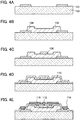
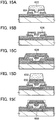
- FIGS. 1A and 1B and FIGS. 2A to 2E Examples of a semiconductor device and a manufacturing method thereof are described with reference to FIGS. 1A and 1B and FIGS. 2A to 2E . Note that in the following description, a power MOS (MIS) FET is used as a semiconductor device.
- MIS power MOS
- FIGS. 1A and 1B illustrate an example of the structure of a semiconductor device.
- FIG 1A corresponds to a cross-sectional view
- FIG 1B corresponds to a plan view
- FIG. 1A corresponds to a cross section taken along line A-B in FIG 1B . Note that in the plan view, some of components are omitted for simplicity.
- the semiconductor device illustrated in FIGS. 1A and 1B includes a substrate 100, a conductive layer 102 functioning as one of a source electrode and a drain electrode, an oxide semiconductor layer 104, a crystal region 106 in the oxide semiconductor layer 104, a conductive layer 108 functioning as the other of the source electrode and the drain electrode, an insulating layer 110 functioning as a gate insulating layer, a conductive layer 112 electrically connected to the conductive layer 108, a conductive layer 114 electrically connected to the conductive layer 102, a conductive layer 116 functioning as a gate electrode, and the like.
- the oxide semiconductor layer 104 contains an oxide semiconductor material whose energy gap is comparatively large as a semiconductor.
- the breakdown voltage e.g., drain breakdown voltage
- the crystal region 106 corresponds to a surface part (an upper layer) of the oxide semiconductor layer 104 and is a region where part of the oxide semiconductor layer 104 is crystallized. With the provision of the crystal region 106, the breakdown voltage (e.g., drain breakdown voltage) of the semiconductor device can be further improved. Note that regions except the crystal region 106 in the oxide semiconductor layer 104 are preferably amorphous; however, such regions may contain crystal grains in amorphous regions or may be microcrystalline.
- the conductive layer 116 functioning as a gate electrode is provided around the conductive layer 108 functioning as the other of the source electrode and the drain electrode and the conductive layer 112 electrically connected to the conductive layer 108, and the conductive layer 102 functioning as one of the source electrode and the drain electrode and the conductive layer 114 electrically connected to the conductive layer 102 are provided around the conductive layer 116 (see FIG 1B ).
- the conductive layer 102 functioning as one of the source electrode and the drain electrode does not overlap with the conductive layer 108 functioning as the other of the source electrode and the drain electrode.
- a and B do not have a region where A occupies the same area as B in a plan view. The same can be said for the other portions in this specification.
- the conductive layer 116 functioning as a gate electrode is provided in a region having a region where the conductive layer 102 and the conductive layer 108 do not overlap with each other. That is, at least part of the conductive layer 116 does not overlap with the conductive layer 102 and the conductive layer 108. In contrast, the other part of the conductive layer 116 may overlap with the conductive layer 102 and the conductive layer 108.
- the conductive layer 108 and the conductive layer 112 are provided in the center, and the conductive layer 116, the conductive layer 102, and the conductive layer 114 are provided around the conductive layer 108 and the conductive layer 112; however, the layout of the semiconductor device is not limited to this. Arrangement of the components can be changed as appropriate within the bounds of not impairing the function of the semiconductor device.
- the conductive layer 112 which is electrically connected to the conductive layer 108 functions as a terminal for electrically connecting the conductive layer 108 to an external wiring or the like; however, the conductive layer 112 is not necessarily provided as long as the conductive layer 108 can be directly connected to an external wiring or the like. The same can be said for the conductive layer 114. Note that in FIGS. 1A and 1B , an external wiring or the like which is electrically connected to the conductive layer 112 is not illustrated.
- An insulating substrate, a semiconductor substrate, a metal substrate, or the like is used as the substrate 100.
- a substrate whose surface is covered with an insulating material or the like can be used.
- the substrate 100 preferably has heat resistance high enough to withstand heating of the oxide semiconductor layer.
- a glass substrate, a quartz substrate, or the like can be used as the insulating substrate.
- an insulating substrate including an organic material such as polyimide, polyamide, polyvinyl phenol, a benzocyclobutene resin, an acrylic resin, or an epoxy resin can be used.
- an insulating substrate including an organic material it is necessary to select an insulating substrate which can withstand the highest temperature in a process.
- a typical example of the semiconductor substrate is a silicon substrate (a silicon wafer). Although there are plural grades of silicon substrates, an inexpensive silicon substrate may be used as long as it has a certain level of flatness. For example, a silicon substrate with a purity of about 6N (99.9999 %) to 7N (99.99999 %) can be used.
- the metal substrate are an aluminum substrate and a copper substrate.
- an insulating layer may be formed over a surface in order to secure insulating properties.
- the metal substrate has high thermal conductivity, the metal substrate is preferably used as a substrate of a high-power semiconductor device such as a power MOSFET with a high calorific value.
- the semiconductor material of the oxide semiconductor layer 104 there is a semiconductor material represented by In M O 3 (ZnO) m (m > 0).
- M denotes one or more metal elements selected from gallium (Ga), iron (Fe), nickel (Ni), manganese (Mn), cobalt (Co), or the like.
- Ga gallium
- Fe iron
- Ni nickel
- Mn manganese
- Co cobalt
- the case where Ga is selected as M includes not only the case where only Ga is used but also the case where Ga and the above metal element other than Ga, such as Ni or Fe, are used.
- a transitional metal element such as Fe or Ni or an oxide of the transitional metal is contained as an impurity element in addition to the metal element contained as M.
- an oxide semiconductor containing at least gallium as M is referred to as an In-Ga-Zn-O-based oxide semiconductor.
- the In-Ga-Zn-O-based oxide semiconductor material has sufficiently high resistance when there is no electric field, can have sufficiently low off-state current, and has a large energy gap (a wide gap); thus, it is favorably used for a high-power semiconductor device such as a power MOSFET.
- the semiconductor material of the oxide semiconductor layer 104 there are an In-Sn-Zn-O-based oxide semiconductor material, an In-Al-Zn-O-based oxide semiconductor material, a Sn-Ga-Zn-O-based oxide semiconductor material, an Al-Ga-Zn-O-based oxide semiconductor material, a Sn-Al-Zn-O-based oxide semiconductor material, an In-Zn-O-based oxide semiconductor material, a Sn-Zn-O-based oxide semiconductor material, an Al-Zn-O-based oxide semiconductor material, an In-O-based oxide semiconductor material, a Sn-O-based oxide semiconductor material, a Zn-O-based oxide semiconductor material, and the like.
- the oxide semiconductor layer 104 (excluding the crystal region 106) preferably has an amorphous structure; however, the oxide semiconductor layer 104 may have an amorphous structure containing a crystal grain, a microcrystalline structure, or the like. Further, the thickness of the oxide semiconductor layer 104 can be set as appropriate depending on a characteristic such as desired breakdown voltage. Specifically, the thickness of the oxide semiconductor layer 104 can be approximately 100 nm to 10 ⁇ m.
- the crystal region 106 preferably has a structure where micro crystals (may be simply referred to as crystal grains) each having a size of 20 nm or less are arranged.
- the crystal region 106 is a region where micro crystals of In 2 Ga 2 ZnO 7 are arranged in a predetermined direction.
- the micro crystals are arranged in such a manner that the c-axis of In 2 Ga 2 ZnO 7 is perpendicular to a plane of a substrate (or a surface of the oxide semiconductor layer), the breakdown voltage of the semiconductor device can be greatly improved. This results from the dielectric constant anisotropy of In 2 Ga 2 ZnO 7 .
- Breakdown voltage in a b-axis direction (or an a-axis direction) can be improved as compared to that in a c-axis direction.
- the size of the micro crystal is just an example, and the present invention is not construed as being limited to the above range.
- the insulating material of the insulating layer 110 functioning as a gate insulating layer can be selected from silicon oxide, silicon nitride, silicon oxynitride, silicon nitride oxide, aluminum oxide, tantalum oxide, or the like. Alternatively, a composite material of these materials may be used.
- the insulating layer 110 may have a single-layer structure or a layered structure including a layer formed using any of the above insulating materials. Note that in general, a MOSFET refers to a field effect transistor containing a metal, an oxide, and a semiconductor; however, an insulating layer used in the semiconductor device of the disclosed invention is not limited to an oxide.
- oxynitride refers to a substance that contains more oxygen (atoms) than nitrogen (atoms).
- silicon oxynitride is a substance that contains oxygen, nitrogen, silicon, and hydrogen at concentrations ranging from 50 to 70 atomic %, 0.5 to 15 atomic %, 25 to 35 atomic %, and 0.1 to 10 atomic %, respectively.
- nitride oxide refers to a substance that contains more nitrogen (atoms) than oxygen (atoms).
- silicon nitride oxide contains oxygen, nitrogen, silicon, and hydrogen at concentrations ranging from 5 to 30 atomic %, 20 to 55 atomic %, 25 to 35 atomic %, and 10 to 25 atomic %, respectively.
- concentrations are concentrations when measurement is performed using Rutherford backscattering spectrometry (RBS) or hydrogen forward scattering spectrometry (HFS). Furthermore, the total of the percentages of the constituent elements does not exceed 100 atomic %.
- the conductive layer 102 functions as the drain electrode; the conductive layer 108 functions as the source electrode; and the conductive layer 116 functions as the gate electrode.
- the conductive layer 112 and the conductive layer 114 function as terminals for realizing electrical connection to an external wiring or the like, the conductive layer 112 and the conductive layer 114 are not essential components.
- the conductive material of each of the conductive layers can be selected from a metal material such as aluminum, copper, molybdenum, titanium, chromium, tantalum, tungsten, neodymium, or scandium; an alloy material containing any of these metal materials as its main component; a nitride containing any of these metal materials; or the like.
- a light-transmitting oxide conductive material such as indium oxide, an alloy of indium oxide and tin oxide, an alloy of indium oxide and zinc oxide, zinc oxide, zinc aluminum oxide, zinc aluminum oxynitride, or zinc gallium oxide can be used.
- the conductive layer may have a single-layer structure or a layered structure including a layer formed using any of the above conductive materials.
- the conductive layer 108 functioning as a source electrode is formed over the oxide semiconductor 104 and in contact with an upper surface of the oxide semiconductor layer 104.
- the conductive layer 102 functioning as a drain electrode is formed under the oxide semiconductor layer 104 and in contact with a lower surface of the oxide semiconductor layer 104.
- the conductive layer 116 functioning as a gate electrode is provided over the insulating layer 110 and generates an electric field in the oxide semiconductor layer 104.
- a negative bias is applied to the conductive layer 108 functioning as a source electrode, and a positive bias is applied to the conductive layer 102 functioning as a drain electrode.
- the oxide semiconductor layer 104 with sufficient thickness is provided between the conductive layer 108 functioning as a source electrode and the conductive layer 102 functioning as a drain electrode.
- the oxide semiconductor layer 104 is formed using an oxide semiconductor material which has a wide gap and sufficiently high resistance when there is no electric field. Therefore, in a condition that a negative bias is applied to the conductive layer 108 and a positive bias is applied to the conductive layer 102, a very small amount of current flows when a bias is not applied to the conductive layer 116 functioning as a gate electrode or a negative bias is applied to the conductive layer 116.
- the breakdown voltage (e.g., drain breakdown voltage) of the semiconductor device can be improved. This results from a larger energy gap of the oxide semiconductor than that of a general semiconductor material.
- the breakdown voltage of the semiconductor device can be further improved.
- the micro crystals are arranged in such a manner that the c-axis of In 2 Ga 2 ZnO 7 is perpendicular to the plane of the substrate (or the surface of the oxide semiconductor layer).
- a direction in which current flows in the semiconductor device is a b-axis direction (or an a-axis direction) of In 2 Ga 2 ZnO 7 , so that the breakdown voltage of the semiconductor device can be improved.
- the crystal of In 2 Ga 2 ZnO 7 is formed so as to have a layered structure of layers which are parallel to the a-axis or the b-axis. That is, the c-axis of In 2 Ga 2 ZnO 7 refers to a direction which is perpendicular to the layer included in the crystal of In 2 Ga 2 ZnO 7 .
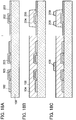
- Steps of manufacturing the semiconductor device illustrated in FIGS. 1A and 1B are described with reference to FIGS. 2A to 2E .
- the conductive layer 102 is formed over the substrate 100 (see FIG 2A ).
- the section ⁇ Substrate> can be referred to for details of the substrate 100.
- the conductive layer 102 is formed in such a manner that a conductive layer containing the conductive material illustrated in the section ⁇ Conductive Layer> is deposited over the substrate 100 by a method such as sputtering or vacuum evaporation, and then, an unnecessary portion is removed by etching with the use of a resist mask formed by photolithography.
- the etching may be either wet etching or dry etching. Note that in order to improve coverage with each component formed over the conductive layer 102, the etching is preferably performed in such a manner that an angle between a side surface of the conductive layer 102 and a bottom surface of the conductive layer 102 is an acute angle.
- the conductive layer 102 has a layered structure of a layer formed using a low-resistant conductive material such as aluminum or copper and a layer formed using a high-melting-point conductive material such as molybdenum, titanium, chromium, tantalum, tungsten, neodymium, or scandium, high conductivity and high heat resistance can be realized, which is preferable.
- a two-layer structure of aluminum and molybdenum, a two-layer structure of copper and molybdenum, a two-layer structure of copper and titanium nitride, a two-layer structure of copper and tantalum nitride, or the like can be used.
- a two-layer structure of titanium nitride and molybdenum may be used.
- a three-layer structure can be used in which aluminum, an alloy of aluminum and silicon, an alloy of aluminum and titanium, an alloy of aluminum and neodymium, or the like is sandwiched between layers of tungsten, tungsten nitride, titanium nitride, titanium, or the like.
- the oxide semiconductor layer 104 including the crystal region 106 is formed so as to cover the conductive layer 102 (see FIG 2B ). Note that the oxide semiconductor layer 104 without the crystal region 106 may be formed.
- the oxide semiconductor layer 104 is formed using any of the oxide semiconductor materials in the section ⁇ Oxide Semiconductor Layer>.
- the oxide semiconductor layer 104 can be deposited by sputtering or the like in a rare gas atmosphere which includes, for example, argon, an oxygen atmosphere, or a mixed gas atmosphere in which a rare gas and oxygen are mixed.
- a rare gas atmosphere which includes, for example, argon, an oxygen atmosphere, or a mixed gas atmosphere in which a rare gas and oxygen are mixed.
- SiO x (x > 0) is contained in the oxide semiconductor layer 104, so that crystallization of the oxide semiconductor layer 104 can be suppressed. This method is effective in obtaining the oxide semiconductor layer 104 with an amorphous structure.
- a distance between the substrate and the target is 100 mm; pressure is 0.6 Pa; DC power is 0.5 kW; and the atmosphere is an oxygen (an oxygen flow rate ratio is 100 %) atmosphere.
- an In-Ga-Zn-O-based amorphous oxide semiconductor layer can be obtained as the oxide semiconductor layer 104.
- a pulse DC power source is used as a power source, a powdered substance (also referred to as a particle or dust) in deposition can be reduced and thickness distribution can be made uniform, which is preferable.
- the thickness of the oxide semiconductor layer 104 can be set as appropriate depending on a characteristic such as desired breakdown voltage.
- the thickness of the oxide semiconductor layer 104 may be approximately 100 nm to 10 ⁇ m.
- the crystal region 106 is formed through heat treatment performed after the formation of the oxide semiconductor layer 104. Note that H 2 , H, OH, or the like contained in the oxide semiconductor layer 104 is eliminated through the heat treatment, so that the heat treatment may be referred to as dehydration treatment or dehydrogenation treatment.
- RTA rapid thermal annealing
- a high-temperature inert gas e.g., nitrogen or a rare gas
- the temperature of the heat treatment is preferably 500 °C or higher.
- the upper limit of the heat treatment temperature is not particularly limited to a certain temperature, it is necessary to set the upper limit within the heat resistance of the substrate 100.
- time for the heat treatment is preferably 1 to 10 minutes.
- RTA treatment is preferably performed at 650 °C for about 3 to 6 minutes. With the RTA treatment, heat treatment can be performed in a short time; thus, the adverse effect of heat on the substrate 100 can be reduced.
- timing of the heat treatment is not limited to the above timing, and the heat treatment can be performed before or after a different step. Further, the number of the heat treatments is not limited to one, and the heat treatment may be performed more than once.
- the purity of an inert gas introduced into a heat treatment apparatus is 6N (99.9999 %, that is, the impurity concentration is 1 ppm or less) or more, preferably 7N (99.99999 %, that is, the impurity concentration is 0.1 ppm or less) or more.
- the surface part in the oxide semiconductor layer 104 is crystallized, so that the crystal region 106 where micro crystals are arranged is formed.
- the other regions of the oxide semiconductor layer 104 have an amorphous structure, a structure where an amorphous structure and a microcrystalline structure are mixed with each other, or a microcrystalline structure.
- the crystal region 106 is part of the oxide semiconductor layer 104, and the oxide semiconductor layer 104 includes the crystal region 106.
- the thickness of the crystal region 106 is preferably 20 nm or less. This is because the properties of the semiconductor device depend on only the crystal region 106 when the crystal region is thick.
- the atmosphere of the cooling process can be, for example, an atmosphere of an oxygen gas, an N 2 O gas, or ultra-dry air (having a dew point of -40 °C or lower, preferably -60 °C or lower).
- the conductive layer 108 is formed in a region over the oxide semiconductor layer 104 that does not overlap with the conductive layer 102 (see FIG 2C ).
- the conductive layer 108 can be formed in a manner similar to that of the conductive layer 102.
- the conductive layer 108 is formed in such a manner that a conductive layer is deposited by a method such as sputtering or vacuum evaporation, and then, an unnecessary portion is removed by etching with the use of a resist mask.
- the etching may be either wet etching or dry etching. In the case where the crystal region 106 is formed in the surface part of the oxide semiconductor layer 104, it is necessary that the crystal region 106 be not removed by the etching.
- etching in which a hydrogen peroxide solution or heated hydrochloric acid is used as an etchant is preferably used.
- etching is performed under a condition that etching selectivity between the conductive material of the conductive layer 108 and the oxide semiconductor material is sufficiently high in this manner, the crystal region 106 in the surface part can remain.
- the insulating layer 110 is formed so as to cover the oxide semiconductor layer 104 and the conductive layer 108 (see FIG 2D ).
- the insulating layer 110 can be formed using the insulating material described in the section ⁇ Insulating Layer>, for example. As a deposition method, CVD, (including plasma-enhanced CVD), sputtering, or the like can be used. Note that the thickness of the insulating layer 110 can be set as appropriate depending on the properties of the semiconductor device; however, the thickness of the insulating layer 110 is preferably 10 nm to 1 ⁇ m.
- openings which reach the conductive layer 102 and the conductive layer 108 are formed by selective removal of the insulating layer 110 or the like, and then, the conductive layer 112 which is electrically connected to the conductive layer 108, the conductive layer 114 which is electrically connected to the conductive layer 102, and the conductive layer 116 are formed (see FIG. 2E ).
- Removal of the insulating layer 110 or the like can be performed by etching with the use of a resist mask.
- the etching may be either wet etching or dry etching.
- the conductive layers 112, 114, and 116 can be formed in a manner similar to those of the other conductive layers.
- each of the conductive layers 112, 114, and 116 is formed in such a manner that a conductive layer is deposited by a method such as sputtering or vacuum evaporation, and then, an unnecessary portion is removed by etching with the use of a resist mask.
- the etching may be either wet etching or dry etching.
- a semiconductor device called a power MOSFET can be manufactured.
- the breakdown voltage of the semiconductor device is improved.
- the breakdown voltage of the semiconductor device can be further improved.
- the productivity of the semiconductor device can be increased and manufacturing cost can be reduced.
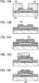
- FIGS. 3A and 3B and FIGS. 4A to 4E different examples of a semiconductor device and a manufacturing method thereof are described with reference to FIGS. 3A and 3B and FIGS. 4A to 4E .
- a semiconductor device described in this example and the semiconductor device in the aforementioned example have a lot in common. Therefore, description of common portions is omitted, and differences are mainly described.
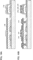
- FIGS. 3A and 3B illustrate a different example of the structure of a semiconductor device.
- FIG 3A corresponds to a cross-sectional view
- FIG 3B corresponds to a plan view.
- FIG 3A corresponds to a cross section taken along line A-B in FIG 3B .
- the semiconductor device illustrated in FIGS. 3A and 3B includes the substrate 100, the conductive layer 102 functioning as one of the source electrode and the drain electrode, the oxide semiconductor layer 104, the crystal region 106 in the oxide semiconductor layer 104, the conductive layer 108 functioning as the other of the source electrode and the drain electrode, the insulating layer 110 functioning as a gate insulating layer, the conductive layer 112 electrically connected to the conductive layer 108, the conductive layer 114 electrically connected to the conductive layer 102, the conductive layer 116 functioning as a gate electrode, and the like.
- the semiconductor device illustrated in FIGS. 3A and 3B differs from the semiconductor device illustrated in FIGS. 1A and 1B in that the oxide semiconductor layer 104 is patterned. Even in the case where the structure in FIGS. 3A and 3B is employed, the semiconductor device illustrated in FIGS. 3A and 3B operates in a manner similar to that of the semiconductor device illustrated in FIGS. 1A and 1B and advantageous effects similar to those of the semiconductor device illustrated in FIGS. 1A and 1B can be obtained.
- Steps of manufacturing the semiconductor device are basically similar to those in FIGS. 2A to 2E .
- the steps of manufacturing the semiconductor device are briefly described below with reference to FIGS. 4A to 4E .
- the conductive layer 102 is formed over the substrate 100 (see FIG 4A ).
- the aforementioned example can be referred to for details.
- the oxide semiconductor layer 104 including the crystal region 106 is formed so as to cover the conductive layer 102 (see FIG. 4B ).
- the formation method of the oxide semiconductor layer 104 is similar to that in the aforementioned example however, the oxide semiconductor layer 104 in this example differs from the oxide semiconductor layer 104 in the aforementioned example in that it is formed so as to cover part of the conductive layer 102.
- the oxide semiconductor layer 104 can be obtained in such a manner that an oxide semiconductor layer (including a crystal region) is deposited by the method illustrated in the aforementioned example for example, and then, the oxide semiconductor layer is patterned. Patterning can be performed by etching with the use of a resist mask. The etching may be either wet etching or dry etching; however, it is preferable to perform the etching so that the crystal region remains.
- the conductive layer 108 is formed in a region over the oxide semiconductor layer 104 that does not overlap with the conductive layer 102 (see FIG 4C ).
- the aforementioned example can be referred to for details.
- the insulating layer 110 is formed so as to cover the oxide semiconductor layer 104 and the conductive layer 108 (see FIG 4D ).
- the aforementioned example can be referred to for details of the insulating layer 110.
- openings which reach the conductive layer 102 and the conductive layer 108 are formed by selective removal of the insulating layer 110 or the like, and then, the conductive layer 112 which is electrically connected to the conductive layer 108, the conductive layer 114 which is electrically connected to the conductive layer 102, and the conductive layer 116 are formed (see FIG 4E ).
- the aforementioned example can be referred to for details.
- a semiconductor device called a power MOSFET can be manufactured.
- the structures, methods, and the like described in this example can be combined with any of the other examples as appropriate.
- FIGS. 5A and 5B and FIGS. 6A to 6D Different examples of a semiconductor device and a manufacturing method thereof are described with reference to FIGS. 5A and 5B and FIGS. 6A to 6D .
- a semiconductor device described in this example and the semiconductor device in the aforementioned example have a lot in common. Therefore, description of common portions is omitted, and differences are mainly described.
- FIGS. 5A and 5B illustrate a different example of the structure of a semiconductor device.
- FIG 5A corresponds to a cross-sectional view
- FIG 5B corresponds to a plan view
- FIG 5A corresponds to a cross section taken along line A-B in FIG 5B .
- the semiconductor device illustrated in FIGS. 5A and 5B corresponds to a semiconductor device where the conductive layer 102 in the semiconductor device described in the aforementioned example is replaced with a conductive layer 109.
- the semiconductor device illustrated in FIGS. 5A and 5B includes the substrate 100, the conductive layer 109 functioning as one of a source electrode and a drain electrode, the oxide semiconductor layer 104, the crystal region 106 in the oxide semiconductor layer 104, the conductive layer 108 functioning as the other of the source electrode and the drain electrode, the insulating layer 110 functioning as a gate insulating layer, the conductive layer 112 electrically connected to the conductive layer 108, the conductive layer 114 electrically connected to the conductive layer 109, the conductive layer 116 functioning as a gate electrode, and the like.
- the conductive layer 109 is formed using the same layer as the conductive layer 108. By replacement of the conductive layer 102 with the conductive layer 109, all the conductive layers are provided over the oxide semiconductor layer 104. Thus, flatness of a surface of the oxide semiconductor layer 104 is improved.
- Steps of manufacturing the semiconductor device are similar to those in FIGS. 2A to 2E and FIGS. 4A to 4E except that the conductive layer 102 is not formed and that the conductive layer 109 is formed at the same time as the conductive layer 108.
- the steps of manufacturing the semiconductor device are briefly described below with reference to FIGS. 6A to 6D .
- the oxide semiconductor layer 104 is formed over the substrate 100 (see FIG 6A ).
- the aforementioned example can be referred to for details of the formation and the like of the oxide semiconductor layer 104.
- the conductive layer 108 and the conductive layer 109 are formed over the oxide semiconductor layer 104 (see FIG 6B ).
- the conductive layer 109 can be formed in a manner similar to that of the conductive layer 108. It should be noted that the conductive layer 108 and the conductive layer 109 are separated from each other. The aforementioned example can be referred to for details of the formation and the like of the conductive layer 108.
- the insulating layer 110 is formed so as to cover the oxide semiconductor layer 104, the conductive layer 108, and the conductive layer 109 (see FIG 6C ).
- the aforementioned example can be referred to for details of the insulating layer 110.
- openings which reach the conductive layer 108 and the conductive layer 109 are formed by selective removal of the insulating layer 110 or the like, and then, the conductive layer 112 which is electrically connected to the conductive layer 108, the conductive layer 114 which is electrically connected to the conductive layer 109, and the conductive layer 116 are formed (see FIG 6D ).
- the aforementioned example can be referred to for details.
- a semiconductor device called a power MOSFET can be manufactured.
- the structures, methods, and the like described in this example can be combined with any of the other examples as appropriate.
- FIGS. 7A to 7C and FIGS. 8A and 8B An example of a method for manufacturing a so-called power MOSFET and a thin film transistor over the same substrate and in similar steps is described with reference to FIGS. 7A to 7C and FIGS. 8A and 8B . Note that an example is described below in which the semiconductor device illustrated in FIGS. 1A and 1B is formed as a power MOSFET.
- Steps of manufacturing the semiconductor device illustrated in this example correspond to steps obtained by addition of a step of manufacturing a thin film transistor to the steps in FIGS. 2A to 2E . That is, basic manufacturing steps are similar to those illustrated in FIGS. 2A to 2E .
- the power MOSFET and the thin film transistor generally have different required properties.
- the size or the like of the power MOSFET and the thin film transistor is preferably set as appropriate depending on the required properties.
- the power MOSFET and the thin film transistor are illustrated on approximately the same scale in FIGS. 7A to 7C and FIGS. 8A and 8B , such a scale is used to facilitate understanding and does not define the relationship of the real size.
- the conductive layer 102 is formed over the substrate 100 (see FIG 7A ).
- the aforementioned example can be referred to for details.
- the oxide semiconductor layer 104 including the crystal region 106 is formed so as to cover the conductive layer 102, and an oxide semiconductor layer 204 including a crystal region 206 that is a component of the thin film transistor is formed (see FIG 7B ).
- Each of the oxide semiconductor layers 104 and 204 can be obtained in such a manner that an oxide semiconductor layer (including a crystal region) is deposited by the method illustrated in the aforementioned example, for example, and then, the oxide semiconductor layer is patterned. Patterning can be performed by etching with the use of a resist mask. The etching may be either wet etching or dry etching; however, it is preferable to perform the etching so that the crystal region in the oxide semiconductor layer remains.
- the conductive layer 108 is formed in a region over the oxide semiconductor layer 104 that does not overlap with the conductive layer 102, and conductive layers 208 and 209 are formed over the oxide semiconductor layer 204 (see FIG 7C ).
- the conductive layer 208 functions as one of a source electrode and a drain electrode of the thin film transistor
- the conductive layer 209 functions as the other of the source electrode and the drain electrode of the thin film transistor. Steps of manufacturing the conductive layers 208 and 209 are similar to those of the conductive layer 108. The aforementioned example can be referred to for details of the steps of manufacturing the conductive layer 108.
- the insulating layer 110 is formed so as to cover the oxide semiconductor layer 104, the conductive layer 108, the oxide semiconductor layer 204, the conductive layer 208, and the conductive layer 209 (see FIG 8A ).
- the insulating layer 110 functions also as a gate insulating layer of the thin film transistor.
- the aforementioned example can be referred to for details of the steps of manufacturing the insulating layer 110.
- openings which reach the conductive layer 102, the conductive layer 108, the conductive layer 208, and the conductive layer 209 are formed by selective removal of the insulating layer 110 or the like, and then, the conductive layer 112 which is electrically connected to the conductive layer 108, the conductive layer 114 which is electrically connected to the conductive layer 102, the conductive layer 116, a conductive layer 212 which is electrically connected to the conductive layer 208, a conductive layer 214 which is electrically connected to the conductive layer 209, and a conductive layer 216 are formed (see FIG 8B ). Steps of manufacturing the conductive layers 212, 214, and 216 are similar to those of the conductive layers 112, 114, and 116. The aforementioned example can be referred to for details.
- the power MOSFET and the thin film transistor can be formed over the same substrate and in similar steps.
- the power MOSFET and the thin film transistor can be formed over the same substrate and in similar steps. Therefore, a variety of integrated circuits and a power circuit can be formed over the same substrate.
- the oxide semiconductor layer 104 of the power MOSFET and the oxide semiconductor layer 204 of the thin film transistor are formed in the same steps; however, the required thickness of the oxide semiconductor layer is different between the power MOSFET and the thin film transistor in some cases. Therefore, the oxide semiconductor layer 104 and the oxide semiconductor layer 204 may be formed in different steps. Specifically, the oxide semiconductor layer 104 and the oxide semiconductor layer 204 may be formed as follows. Steps of manufacturing the oxide semiconductor layers are divided into two stages; one of the oxide semiconductor layer 104 and the oxide semiconductor layer 204 is manufactured in a first stage; and the other of the oxide semiconductor layer 104 and the oxide semiconductor layer 204 is manufactured in a second stage. Alternatively, a thick oxide semiconductor layer is selectively made thin by etching or the like so that the oxide semiconductor layer 104 and the oxide semiconductor layer 204 are manufactured.
- the insulating layers 110 of the power MOSFET and the thin film transistor are separately formed so as to have different thicknesses.
- the insulating layers 110 are formed as follows. Steps of manufacturing the insulating layers are divided into two stages; one of an insulating layer formed over the oxide semiconductor layer 104 and an insulating layer formed over the oxide semiconductor layer 204 is manufactured in a first stage; and the other of the insulating layer formed over the oxide semiconductor layer 104 and the insulating layer formed over the oxide semiconductor layer 204 is manufactured in a second stage.
- a thick insulating layer is selectively made thin by etching or the like so that the insulating layer formed over the oxide semiconductor layer 104 and the insulating layer formed over the oxide semiconductor layer 204 are manufactured.
- FIG 9 An example of a circuit including a semiconductor device of the disclosed invention is described with reference to FIG 9 and FIGS. 10A to 10C .
- a DC-DC converter which is an example of a power circuit (e.g., a power conversion circuit), is described below.
- the DC-DC converter is a circuit for converting DC voltage into different DC voltage.
- Typical conversion methods of the DC-DC converter are a linear method and a switching method. Since a switching-type DC-DC converter has high conversion efficiency, such a DC-DC converter is preferable when power saving of an electronic device is to be achieved.
- a switching-type DC-DC converter especially a chopper DC-DC converter is described.
- a DC-DC converter illustrated in FIG 9 includes a power source 300, a reference voltage generation circuit 302, a reference current generation circuit 304, an error amplifier 306, a PWM buffer 308, a triangle wave generation circuit 310, a coil 312, a power MOSFET 314, a diode 316, a capacitor 318, a resistor 320, a resistor 322, and the like. Note that here, an n-channel power MOSFET is used as the power MOSFET 314.
- the reference voltage generation circuit 302 generates a variety of reference voltages ( V ref ) ⁇
- the reference current generation circuit 304 generates reference current ( I ref ) or bias current with the use of reference voltage ( V ref ) generated in the reference voltage generation circuit 302.
- the error amplifier 306 integrates a difference between the reference voltage ( V ref ) generated in the reference voltage generation circuit 302 and feedback voltage ( V FB ) and outputs the value of integral to the PWM buffer 308.
- the triangle wave generation circuit 310 generates a triangle wave from the reference voltage ( V ref ) and the reference current ( I ref ) and outputs the triangle wave to the PWM buffer 308.
- the PWM buffer 308 compares an output from the error amplifier 306 and the triangle wave from the triangle wave generation circuit 310 and outputs a pulse signal to the power MOSFET 314.
- the n-channel power MOSFET 314 is turned off, and the potential of the input side of the diode 316 rises. Therefore, in a period during which the pulse signal has a low potential, the output voltage ( V OUT ) is gradually increased.
- the coil 312 is provided for reducing changes in current due to switching of the power MOSFET 314. Further, the capacitor 318 is provided for suppressing drastic fluctuation in the output voltage ( V OUT ) . Furthermore, the resistors 320 and 322 are provided for generating the feedback voltage ( V FB ) from the output voltage ( V OUT ) .
- FIGS. 10A to 10C illustrate examples of output waveforms of circuits included in the DC-DC converter.
- FIG 10A illustrates a triangle wave 350 output from the triangle wave generation circuit 310.
- FIG 10B illustrates an output waveform 352 from the error amplifier 306.
- FIG. 10C illustrates a pulse signal 354 generated in the PWM buffer 308.
- the PWM buffer 308 compares these waves with each other and generates the pulse signal 354. Then, the pulse signal 354 is output to the power MOSFET 314 and the level of the output voltage ( V OUT ) is determined.
- a power MOSFET of the disclosed invention can be applied to a DC-DC converter.
- the power MOSFET of the disclosed invention has high breakdown voltage, and the reliability of a DC-DC converter including the power MOSFET can be improved. Further, the manufacturing cost of the power MOSFET of the disclosed invention is suppressed, so that the manufacturing cost of the DC-DC converter including the power MOSFET is suppressed.
- the DC-DC converter illustrated in this example is just an example of a power circuit including the semiconductor device of the disclosed invention. Needless to say, the semiconductor device of the disclosed invention can be used in a different circuit. The structures, methods, and the like described in this can be combined with any of the other examples as appropriate.
- FIG 11 An example of a solar photovoltaic system provided with an inverter formed using a semiconductor device of the disclosed invention is described with reference to FIG 11 . Note that here, an example of the structure of a household solar photovoltaic system is described.
- the household solar photovoltaic system illustrated in FIG. 11 is a system where a method for supplying power is changed depending on the condition of photovoltaic power generation. For example, when photovoltaic power generation is performed (e.g., in the case of a clear sky), power generated by photovoltaic power generation is consumed at home, and surplus power is supplied to a distribution line 414 from a power company. In contrast, when the amount of power generated by photovoltaic power generation is insufficient (e.g., in the case of night or rain), electricity is supplied from the distribution line 414 and is consumed at home.
- the household solar photovoltaic system illustrated in FIG 11 includes a solar cell panel 400 for converting sunlight into power (DC power), an inverter 404 for converting the DC power into AC power, and the like.
- AC power output from the inverter 404 is used as power for operating a variety of electric appliances 410.
- a DC switch 402 is provided for selecting whether the solar cell panel 400 and the inverter 404 are connected or disconnected to each other.
- An AC switch 408 is provided for selecting whether a transformer 412 which is connected to the distribution line 414 and a distribution board 406 are connected or disconnected to each other.
- examples of a transistor especially, a thin film transistor as a semiconductor device and a manufacturing method thereof are described with reference to FIGS. 12A to 12F and FIGS. 13A to 13E .
- a semiconductor device described below is a semiconductor device with a novel structure. An oxide semiconductor layer having a crystal region in a surface part is used in the semiconductor device. The semiconductor device controls current with two conductive layers.
- a conductive layer 502 is deposited over a substrate 500 (see FIG 12A ), and a resist mask 504 is selectively formed over the conductive layer 502. Then, the conductive layer 502 is selectively etched using the resist mask 504, so that a conductive layer 506 is formed (see FIG 12B ). After the resist mask 504 is removed, an insulating layer 508 is formed so as to cover the conductive layer 506 (see FIG 12C ).
- the conductive layer 506 has a function of controlling an electric field in an oxide semiconductor layer. Further, the conductive layer 506 has a function of blocking an external electric field which adversely affects the operation of a transistor.
- the aforementioned examples can be referred to for materials, manufacturing methods, and the like of the components.
- the conductive layer 506 may be formed over the entire upper surface of the substrate. Alternatively, the conductive layer 506 may be formed below the entire lower surface of the oxide semiconductor layer.
- an oxide semiconductor layer 510 is deposited over the insulating layer 508 (see FIG 12D ), and a resist mask 512 is selectively formed over the oxide semiconductor layer 510. Then, the oxide semiconductor layer 510 is selectively etched using the resist mask 512, so that an oxide semiconductor layer 514 is formed (see FIG. 12E ). Note that after the oxide semiconductor layer 514 is formed, the resist mask 512 is removed.
- the aforementioned embodiment can be referred to for details of the oxide semiconductor layer. Further, the aforementioned embodiment can be referred to for details of the other components.
- the thickness of the oxide semiconductor layer 510 can be set as appropriate depending on a desired property. In the case where the oxide semiconductor layer 510 is used for a thin film transistor, for example, the thickness of the oxide semiconductor layer 510 is preferably about 20 nm to 2 ⁇ m.
- a conductive layer 516 is deposited so as to cover the oxide semiconductor layer 514 (see FIG. 12F ), and a resist mask 518 and a resist mask 520 are selectively formed over the conductive layer 516. Then, the conductive layer 516 is selectively etched using the resist masks, so that a conductive layer 522 which functions as one of a source electrode and a drain electrode and a conductive layer 524 which functions as the other of the source electrode and the drain electrode are formed (see FIG 13A ). Note that after the conductive layer 522 and the conductive layer 524 are formed, the resist mask 518 and the resist mask 520 are removed.
- the aforementioned embodiment can be referred to for details of the above components.
- an insulating layer 526 which functions as a gate insulating layer is formed so as to cover the oxide semiconductor layer 514, the conductive layer 522, and the conductive layer 524 (see FIG 13B ).
- a conductive layer 528 is deposited over the insulating layer 526 (see FIG 13C ), and a resist mask 530 is selectively formed over the conductive layer 528.
- the conductive layer 528 is selectively etched using the resist mask 530, so that a conductive layer 532 which functions as a gate electrode is formed (see FIG 13D ).
- the resist mask 530 is removed.
- a transistor 550 which includes the conductive layer 506 formed over the substrate 500, the insulating layer 508 which covers the conductive layer 506, the oxide semiconductor layer 514 formed over the insulating layer 508 that overlaps with part of the conductive layer 506 and has a crystal region in a surface part, the conductive layers 522 and 524 formed in contact with the oxide semiconductor layer 514, the insulating layer 526 which covers the oxide semiconductor layer 514 and the conductive layers 522 and 524, and the conductive layer 532 formed over the insulating layer 526 that overlaps with part of the oxide semiconductor layer 514, is provided (see FIG 13E ). Note that it can be said that the transistor 550 is a novel semiconductor device because an oxide semiconductor layer having a crystal region in a surface part is used and current is controlled with two conductive layers.
- an impurity e.g., hydrogen (including water)
- hydrogen including water
- a conductive layer is formed below an oxide semiconductor layer in addition to a conductive layer functioning as a so-called gate electrode, an external electric field can be blocked, so that the adverse effect of the external electric field on the semiconductor device can be reduced. Therefore, generation of parasitic channels due to accumulation of electric charge on the substrate side of the oxide semiconductor layer and fluctuation in the threshold voltage can be prevented.
- examples of a transistor as a semiconductor device and a manufacturing method thereof are described with reference to FIGS. 14A to 14F and FIGS. 15A to 15E .
- a conductive layer 602 is deposited over a substrate 600 (see FIG 14A ), and a resist mask 604 is selectively formed over the conductive layer 602. Then, the conductive layer 602 is selectively etched using the resist mask 604, so that a conductive layer 606 is formed (see FIG 14B ). After the resist mask 604 is removed, an insulating layer 608 is formed so as to cover the conductive layer 606 (see FIG 14C ).
- the conductive layer 606 has a function of controlling an electric field in an oxide semiconductor layer. Further, the conductive layer 606 has a function of blocking an external electric field which adversely affects the operation of a transistor.
- the aforementioned examples can be referred to for materials, manufacturing methods, and the like of the components.
- the conductive layer 606 may be formed over the entire upper surface of the substrate. Alternatively, the conductive layer 606 may be formed below the entire lower surface of the oxide semiconductor layer.
- a conductive layer 610 is deposited over the insulating layer 608 (see FIG 14D ), and a resist mask 612 and a resist mask 614 are selectively formed over the conductive layer 610. Then, the conductive layer 610 is selectively etched using the resist masks, so that a conductive layer 616 which functions as one of a source electrode and a drain electrode and a conductive layer 618 which functions as the other of the source electrode and the drain electrode are formed (see FIG. 14E ). Note that after the 5 conductive layer 616 and the conductive layer 618 are formed, the resist mask 612 and the resist mask 614 are removed.
- the aforementioned embodiment can be referred to for details of the above components.
- an oxide semiconductor layer 620 is deposited so as to cover the 10 conductive layer 616 and the conductive layer 618 (see FIG. 14F ), and a resist mask 622 is selectively formed over the oxide semiconductor layer 620. Then, the oxide semiconductor layer 620 is selectively etched using the resist mask 622, so that an oxide semiconductor layer 624 is formed (see FIG. 15A ). Note that after the oxide semiconductor layer 624 is formed, the resist mask 622 is removed.
- the 15 aforementioned embodiment can be referred to for details of the oxide semiconductor layer. Further, the aforementioned embodiment can be referred to for details of the other components.
- the thickness of the oxide semiconductor layer 620 can be set as appropriate depending on a desired property. In the case where the oxide semiconductor layer 620 is used for a thin film transistor, for example, the thickness of 20 the oxide semiconductor layer 620 is preferably about 20 nm to 2 ⁇ m.
- an insulating layer 626 which functions as a gate insulating layer is formed so as to cover the conductive layer 616, the conductive layer 618, and the oxide semiconductor layer 624 (see FIG. 15B ).
- a conductive layer 628 is deposited 25 over the insulating layer 626 (see FIG. 15C ), and a resist mask 630 is selectively formed over the conductive layer 628.
- the conductive layer 628 is selectively etched using the resist mask 630, so that a conductive layer 632 which functions as a gate electrode is formed (see FIG. 15D ).
- the resist mask 630 is removed.
- the aforementioned embodiment can be referred to for 30 details of the above components.
- a transistor 650 which includes the conductive layer 606 formed over the substrate 600, the insulating layer 608 which covers the conductive layer 606, the oxide semiconductor layer 624 formed over the insulating layer 608 that overlaps with part of the conductive layer 606 and has a crystal region in a surface part, the conductive layers 616 and 618 formed in contact with the oxide semiconductor layer 624, the insulating layer 626 which covers the oxide semiconductor layer 624 and the conductive layers 616 and 618, and the conductive layer 632 formed over the insulating layer 626 that overlaps with part of the oxide semiconductor layer 624, is provided (see FIG 15E ). Note that it can be said that the transistor 650 is a novel semiconductor device because an oxide semiconductor layer having a crystal region in a surface part is used and current is controlled with two conductive layers.
- an impurity e.g., hydrogen (including water)
- hydrogen including water
- a conductive layer is formed below an oxide semiconductor layer in addition to a conductive layer functioning as a so-called gate electrode, an external electric field can be blocked, so that the adverse effect of the external electric field on the semiconductor device can be reduced. Therefore, generation of parasitic channels due to accumulation of electric charge on the substrate side of the oxide semiconductor layer and fluctuation in the threshold voltage can be prevented.
- FIGS. 16A to 16C and FIGS. 17A and 17B An example of a method for manufacturing a so-called power MOSFET and a thin film transistor over the same substrate and in similar steps is described with reference to FIGS. 16A to 16C and FIGS. 17A and 17B . Note that steps of manufacturing a semiconductor device in this example and the steps in the aforementioned embodiment have a lot in common, so that description of common portions is omitted.
- steps of manufacturing the semiconductor device in this example differs from the steps of manufacturing the semiconductor device in the aforementioned embodiment in that a conductive layer for controlling an electric field in an oxide semiconductor layer is formed below the oxide semiconductor layer.
- the conductive layer 102 is formed over the substrate 100, and a conductive layer 202 which is a component of a thin film transistor is formed. Then, an insulating layer 203 which covers the conductive layer 202 is formed (see FIG 16A ).
- the aforementioned embodiment can be referred to for details.
- the conductive layer 202 is formed in steps similar to those of the conductive layer 102 and has a function of controlling an electric field in an oxide semiconductor layer. It is preferable that the conductive layer 102 be not covered with the insulating layer 203.
- the insulating layer 203 can be formed in such a manner that an insulating layer is formed over the substrate 100 and is patterned, for example.
- the oxide semiconductor layer 104 including the crystal region 106 is formed so as to cover the conductive layer 102, and the oxide semiconductor layer 204 including the crystal region 206 is formed over the insulating layer 203 (see FIG 16B ).
- the conductive layer 108 is formed in a region over the oxide semiconductor layer 104 that does not overlap with the conductive layer 102, and the conductive layers 208 and 209 are formed over the oxide semiconductor layer 204 (see FIG. 16C ).
- the aforementioned example can be referred to for details.
- the insulating layer 110 is formed so as to cover the oxide semiconductor layer 104, the conductive layer 108, the oxide semiconductor layer 204, the conductive layer 208, and the conductive layer 209 (see FIG 17A ); openings which reach the conductive layers 102, 108, 202, 208, and 209 are formed by selective removal of the insulating layer 110 or the like; then, the conductive layer 112 electrically connected to the conductive layer 108, the conductive layer 114 electrically connected to the conductive layer 102, the conductive layer 116, a conductive layer (not illustrated) electrically connected to the conductive layer 202, the conductive layer 212 electrically connected to the conductive layer 208, the conductive layer 214 electrically connected to the conductive layer 209, the conductive layer 216, and the like are formed (see FIG 17B ).
- the conductive layer 202 and the conductive layer 216 may be electrically connected to each other; however, in order to control an electric field, the conductive layer 202 and the conductive layer 216 are not necessarily electrically connected to each other.
- the potential of the conductive layer 202 any of a floating potential, a fixed potential, and a potential which fluctuates differently from the potential of the conductive layer 216 can be used.
- the power MOSFET and the thin film transistor can be formed over the same substrate and in similar steps.
- a conductive layer is formed below an oxide semiconductor layer in addition to a conductive layer functioning as a so-called gate electrode, an external electric field can be blocked, so that the adverse effect of the external electric field on the semiconductor device can be reduced. Therefore, generation of parasitic channels due to accumulation of electric charge on the substrate side of the oxide semiconductor layer and fluctuation in the threshold voltage can be prevented.
- FIGS. 18A to 18C and FIGS. 19A and 19B a different example of a method for manufacturing a so-called power MOSFET and a thin film transistor over the same substrate and in similar steps is described with reference to FIGS. 18A to 18C and FIGS. 19A and 19B .
- steps of manufacturing a semiconductor device in this example and the steps in the aforementioned example have a lot in common, so that description of common portions is omitted.
- steps of manufacturing the semiconductor device in this example differs from the steps of manufacturing the semiconductor device in the aforementioned example in that a conductive layer for controlling an electric field is formed below an oxide semiconductor layer of a power MOSFET.
- the conductive layer 102 and a conductive layer 103 are formed over the substrate 100, and the conductive layer 202 which is a component of a thin film transistor is formed. Then, the insulating layer 203 which covers the conductive layers 103 and 202 is formed (see FIG. 18A ).
- the aforementioned example can be referred to for details. Note that each of the conductive layers 103 and 202 is formed in steps similar to those of the conductive layer 102 and has a function of controlling an electric field in an oxide semiconductor layer. It is preferable that the conductive layer 102 be not covered with the insulating layer 203.
- the insulating layer 203 can be formed in such a manner that an insulating layer is formed over the substrate 100 and is patterned, for example.
- the oxide semiconductor layer 104 including the crystal region 106 is formed so as to cover the conductive layer 102 and the insulating layer 203, and the oxide semiconductor layer 204 including the crystal region 206 is formed over the insulating layer 203 (see FIG. 18B ).
- the conductive layer 108 is formed in a region over the oxide semiconductor layer 104 that does not overlap with the conductive layer 102, and the conductive layers 208 and 209 are formed over the oxide semiconductor layer 204 (see FIG 18C ).
- the aforementioned example can be referred to for details.
- the insulating layer 110 is formed so as to cover the oxide semiconductor layer 104, the conductive layer 108, the oxide semiconductor layer 204, the conductive layer 208, and the conductive layer 209 (see FIG 19A ); openings which reach the conductive layers 102, 103, 108, 202, 208, and 209 are formed by selective removal of the insulating layer 110 or the like; then, the conductive layer 112 electrically connected to the conductive layer 108, the conductive layer 114 electrically connected to the conductive layer 102, a conductive layer (not illustrated) electrically connected to the conductive layer 103, the conductive layer 116, a conductive layer (not illustrated) electrically connected to the conductive layer 202, the conductive layer 212 electrically connected to the conductive layer 208, the conductive layer 214 electrically connected to the conductive layer 209, the conductive layer 216, and the like are formed (see FIG.
- the conductive layers 103 and 116 or the conductive layers 202 and 216 may be electrically connected to each other; however, in order to control an electric field, the conductive layers 103 and 116 or the conductive layers 202 and 216 are not necessarily electrically connected to each other.
- a potential of the conductive layer 103 or the potential of the conductive layer 202 any of a floating potential, a fixed potential, and a potential which fluctuates differently from a potential of the conductive layer 116 or the potential of the conductive layer 216 can be used.
- the power MOSFET and the thin film transistor can be formed over the same substrate and in similar steps.
- a conductive layer is formed below an oxide semiconductor layer in addition to a conductive layer functioning as a so-called gate electrode, an external electric field can be blocked, so that the adverse effect of the external electric field on the semiconductor device can be reduced. Therefore, generation of parasitic channels due to accumulation of electric charge on the substrate side of the oxide semiconductor layer and fluctuation in the threshold voltage can be prevented.
Claims (10)
- Dispositif à semi-conducteur comprenant:une première couche conductrice (502) au-dessus d'un substrat (500);une première couche isolante (508) au-dessus de la première couche conductrice (502);une couche d'oxyde semi-conducteur (514) au-dessus de la première couche isolante, la couche d'oxyde semi-conducteur (514) se superposant à la première couche conductrice;une seconde couche conductrice (522) en contact avec la couche d'oxyde semi-conducteur (514);une troisième couche conductrice (524) en contact avec la couche d'oxyde semi-conducteur;une seconde couche isolante (526) au-dessus de la couche d'oxyde semi-conducteur (514), de la seconde couche conductrice (522) et de la troisième couche conductrice (524); etune quatrième couche conductrice (528) au-dessus de la seconde couche isolante (526), la quatrième couche conductrice (528) se superposant à une partie de la couche d'oxyde semi-conducteur; etdans lequel la première couche conductrice (502) a une fonction de commander un champ électrique dans la couche d'oxyde semi-conducteur,dans lequel la seconde couche conductrice (522) sert de l'un d'une électrode de source et d'une électrode de drain,dans lequel la troisième couche conductrice (524) sert de l'autre de l'électrode de source et de l'électrode de drain,dans lequel la quatrième couche conductrice sert d'électrode de grille,dans lequel la couche d'oxyde semi-conducteur comprend une première région et une seconde région, la première région étant située au-dessus de la seconde région,dans lequel la première région de la couche d'oxyde semi-conducteur et la seconde région de la couche d'oxyde semi-conducteur contiennent de l'indium, du gallium et du zinc,dans lequel la première région comprend un cristal, et l'axe c du cristal est substantiellement perpendiculaire à un plan du substrat ou à une surface de la couche d'oxyde semi-conducteur,dans lequel la seconde région a une cristallinité inférieure à celle de la première région, etdans lequel le cristal dans la première région dans la couche d'oxyde semi-conducteur (514) est un cristal d'In2Ga2ZnO7.
- Dispositif à semi-conducteur selon la revendication 1, dans lequel une région excepté une région comprenant le cristal dans la couche d'oxyde semi-conducteur comporte une structure amorphe.
- Dispositif à semi-conducteur selon la revendication 1, dans lequel l'une de la seconde couche conductrice (522) et de la troisième couche conductrice (524) est connectée électriquement à la couche d'oxyde semi-conducteur (514) sur une surface supérieure ou une surface inférieure de la couche d'oxyde semi-conducteur (514).
- Dispositif à semi-conducteur selon la revendication 1, dans lequel la couche d'oxyde semi-conducteur contient un matériau d'oxyde semi-conducteur basé d'In-Ga-Zn-O.
- Procédé de fabrication d'un dispositif à semi-conducteur, le procédé comprenant les étapes de:former une première couche conductrice (502) au-dessus d'un substrat (500);former une première couche isolante (508) couvrant la première couche conductrice (502);former une couche d'oxyde semi-conducteur (514) au-dessus de la première couche isolante (508), la couche d'oxyde semi-conducteur (514) se superposant à la première couche conductrice (502);former une région cristalline dans une surface supérieure de la couche d'oxyde semi-conducteur (514) par un traitement thermique de la couche d'oxyde semi-conducteur (514);former une seconde couche conductrice (522) et une troisième couche conductrice (524) qui sont en contact avec la couche d'oxyde semi-conducteur (514);former une seconde couche isolante (526) au-dessus de la couche d'oxyde semi-conducteur (514), de la seconde couche conductrice (522) et de la troisième couche conductrice (524); etformer une quatrième couche conductrice (528) au-dessus de la seconde couche isolante (526), la quatrième couche conductrice (528) se superposant à une partie de la couche d'oxyde semi-conducteur,dans lequel la première couche conductrice (502) a une fonction de commander un champ électrique dans la couche d'oxyde semi-conducteur,dans lequel la seconde couche conductrice (522) sert de l'un d'une électrode de source et d'une électrode de drain,dans lequel la troisième couche conductrice (524) sert de l'autre de l'électrode de source et de l'électrode de drain,dans lequel la quatrième couche conductrice sert d'électrode de grille,dans lequel la couche d'oxyde semi-conducteur comprend une première région et une seconde région, la première région étant située au-dessus de la seconde région,dans lequel la première région de la couche d'oxyde semi-conducteur et la seconde région de la couche d'oxyde semi-conducteur contiennent de l'indium, du gallium et du zinc,dans lequel la première région comprend un cristal, et l'axe c du cristal est substantiellement perpendiculaire à un plan du substrat ou à une surface de la couche d'oxyde semi-conducteur,dans lequel la seconde région a une cristallinité inférieure à celle de la première région, etdans lequel le cristal dans la première région dans la couche d'oxyde semi-conducteur (514) est un cristal d'In2Ga2ZnO7.
- Procédé de fabrication d'un dispositif à semi-conducteur, selon la revendication 5, dans lequel la région cristalline est formée par un traitement thermique afin que la température de la couche d'oxyde semi-conducteur soit 500 °C ou plus.
- Procédé de fabrication d'un dispositif à semi-conducteur, selon la revendication 5, dans lequel la couche d'oxyde semi-conducteur (514) est formée par pulvérisation cathodique utilisant une cible basée d'In-Ga-Zn-O.
- Dispositif à semi-conducteur selon la revendication 1, dans lequel une surface supérieure de la couche d'oxyde semi-conducteur a une région cristalline.
- Dispositif à semi-conducteur selon la revendication 1, dans lequel la seconde région comporte une structure amorphe.
- Dispositif à semi-conducteur selon la revendication 1, dans lequel le cristal a une taille de 20 nm ou moins.
Applications Claiming Priority (2)
| Application Number | Priority Date | Filing Date | Title |
|---|---|---|---|
| JP2009235604 | 2009-10-09 | ||
| PCT/JP2010/065990 WO2011043170A1 (fr) | 2009-10-09 | 2010-09-09 | Dispositif à semi-conducteur et procédé de fabrication associé |
Publications (3)
| Publication Number | Publication Date |
|---|---|
| EP2486593A1 EP2486593A1 (fr) | 2012-08-15 |
| EP2486593A4 EP2486593A4 (fr) | 2014-04-23 |
| EP2486593B1 true EP2486593B1 (fr) | 2017-02-01 |
Family
ID=43854111
Family Applications (1)
| Application Number | Title | Priority Date | Filing Date |
|---|---|---|---|
| EP10821841.3A Not-in-force EP2486593B1 (fr) | 2009-10-09 | 2010-09-09 | Dispositif à semi-conducteur et procédé de fabrication associé |
Country Status (7)
| Country | Link |
|---|---|
| US (4) | US9006728B2 (fr) |
| EP (1) | EP2486593B1 (fr) |
| JP (3) | JP5697396B2 (fr) |
| KR (3) | KR101959693B1 (fr) |
| CN (1) | CN102576737B (fr) |
| TW (2) | TWI508185B (fr) |
| WO (1) | WO2011043170A1 (fr) |
Families Citing this family (19)
| Publication number | Priority date | Publication date | Assignee | Title |
|---|---|---|---|---|
| EP2486593B1 (fr) | 2009-10-09 | 2017-02-01 | Semiconductor Energy Laboratory Co., Ltd. | Dispositif à semi-conducteur et procédé de fabrication associé |
| KR102065330B1 (ko) | 2009-10-16 | 2020-01-13 | 가부시키가이샤 한도오따이 에네루기 켄큐쇼 | 액정 표시 장치의 제작 방법 |
| KR101959370B1 (ko) | 2009-11-06 | 2019-03-19 | 가부시키가이샤 한도오따이 에네루기 켄큐쇼 | 반도체 장치 및 반도체 장치의 제작 방법 |
| CN103746001B (zh) | 2009-12-04 | 2017-05-03 | 株式会社半导体能源研究所 | 显示装置 |
| WO2011081009A1 (fr) | 2009-12-28 | 2011-07-07 | Semiconductor Energy Laboratory Co., Ltd. | Procédé de fabrication d'un dispositif semi-conducteur |
| US8803143B2 (en) * | 2010-10-20 | 2014-08-12 | Semiconductor Energy Laboratory Co., Ltd. | Thin film transistor including buffer layers with high resistivity |
| JP5975635B2 (ja) | 2010-12-28 | 2016-08-23 | 株式会社半導体エネルギー研究所 | 半導体装置 |
| US8709889B2 (en) * | 2011-05-19 | 2014-04-29 | Semiconductor Energy Laboratory Co., Ltd. | Semiconductor memory device and manufacturing method thereof |
| SG10201505586UA (en) * | 2011-06-17 | 2015-08-28 | Semiconductor Energy Lab | Semiconductor device and method for manufacturing the same |
| JP6116149B2 (ja) | 2011-08-24 | 2017-04-19 | 株式会社半導体エネルギー研究所 | 半導体装置 |
| US8698137B2 (en) | 2011-09-14 | 2014-04-15 | Semiconductor Energy Laboratory Co., Ltd. | Semiconductor device |
| US9112037B2 (en) * | 2012-02-09 | 2015-08-18 | Semiconductor Energy Laboratory Co., Ltd. | Semiconductor device |
| US9312390B2 (en) | 2012-07-05 | 2016-04-12 | Semiconductor Energy Laboratory Co., Ltd. | Remote control system |
| JP2014045175A (ja) | 2012-08-02 | 2014-03-13 | Semiconductor Energy Lab Co Ltd | 半導体装置 |
| US10529740B2 (en) * | 2013-07-25 | 2020-01-07 | Semiconductor Energy Laboratory Co., Ltd. | Semiconductor device including semiconductor layer and conductive layer |
| US20150177311A1 (en) * | 2013-12-19 | 2015-06-25 | Intermolecular, Inc. | Methods and Systems for Evaluating IGZO with Respect to NBIS |
| TWI535034B (zh) * | 2014-01-29 | 2016-05-21 | 友達光電股份有限公司 | 畫素結構及其製作方法 |
| US9722090B2 (en) * | 2014-06-23 | 2017-08-01 | Semiconductor Energy Laboratory Co., Ltd. | Semiconductor device including first gate oxide semiconductor film, and second gate |
| JP6448311B2 (ja) * | 2014-10-30 | 2019-01-09 | 株式会社ジャパンディスプレイ | 半導体装置 |
Family Cites Families (204)
| Publication number | Priority date | Publication date | Assignee | Title |
|---|---|---|---|---|
| JPS60198861A (ja) | 1984-03-23 | 1985-10-08 | Fujitsu Ltd | 薄膜トランジスタ |
| JPH0244256B2 (ja) | 1987-01-28 | 1990-10-03 | Kagaku Gijutsucho Mukizaishitsu Kenkyushocho | Ingazn2o5deshimesarerurotsuhoshokeinosojokozoojusurukagobutsuoyobisonoseizoho |
| JPH0244258B2 (ja) | 1987-02-24 | 1990-10-03 | Kagaku Gijutsucho Mukizaishitsu Kenkyushocho | Ingazn3o6deshimesarerurotsuhoshokeinosojokozoojusurukagobutsuoyobisonoseizoho |
| JPS63210023A (ja) | 1987-02-24 | 1988-08-31 | Natl Inst For Res In Inorg Mater | InGaZn↓4O↓7で示される六方晶系の層状構造を有する化合物およびその製造法 |
| JPH0244260B2 (ja) | 1987-02-24 | 1990-10-03 | Kagaku Gijutsucho Mukizaishitsu Kenkyushocho | Ingazn5o8deshimesarerurotsuhoshokeinosojokozoojusurukagobutsuoyobisonoseizoho |
| JPH0244262B2 (ja) | 1987-02-27 | 1990-10-03 | Kagaku Gijutsucho Mukizaishitsu Kenkyushocho | Ingazn6o9deshimesarerurotsuhoshokeinosojokozoojusurukagobutsuoyobisonoseizoho |
| JPH0244263B2 (ja) | 1987-04-22 | 1990-10-03 | Kagaku Gijutsucho Mukizaishitsu Kenkyushocho | Ingazn7o10deshimesarerurotsuhoshokeinosojokozoojusurukagobutsuoyobisonoseizoho |
| JP2653092B2 (ja) * | 1988-03-25 | 1997-09-10 | セイコーエプソン株式会社 | 相補型薄膜トランジスタ及びその製造方法 |
| JP2963529B2 (ja) | 1990-10-29 | 1999-10-18 | シャープ株式会社 | アクティブマトリクス表示装置 |
| JPH05251705A (ja) | 1992-03-04 | 1993-09-28 | Fuji Xerox Co Ltd | 薄膜トランジスタ |
| JPH07176749A (ja) * | 1993-12-20 | 1995-07-14 | Sharp Corp | 薄膜トランジスタ |
| JP3947575B2 (ja) * | 1994-06-10 | 2007-07-25 | Hoya株式会社 | 導電性酸化物およびそれを用いた電極 |
| JP3479375B2 (ja) | 1995-03-27 | 2003-12-15 | 科学技術振興事業団 | 亜酸化銅等の金属酸化物半導体による薄膜トランジスタとpn接合を形成した金属酸化物半導体装置およびそれらの製造方法 |
| EP0820644B1 (fr) * | 1995-08-03 | 2005-08-24 | Koninklijke Philips Electronics N.V. | Dispositif a semi-conducteur pourvu d'un element de commutation transparent |
| JPH0996836A (ja) | 1995-09-29 | 1997-04-08 | Toshiba Corp | 液晶表示装置 |
| JP3625598B2 (ja) * | 1995-12-30 | 2005-03-02 | 三星電子株式会社 | 液晶表示装置の製造方法 |
| US6211928B1 (en) * | 1996-03-26 | 2001-04-03 | Lg Electronics Inc. | Liquid crystal display and method for manufacturing the same |
| DE19712233C2 (de) | 1996-03-26 | 2003-12-11 | Lg Philips Lcd Co | Flüssigkristallanzeige und Herstellungsverfahren dafür |
| US6001539A (en) | 1996-04-08 | 1999-12-14 | Lg Electronics, Inc. | Method for manufacturing liquid crystal display |
| US6188452B1 (en) * | 1996-07-09 | 2001-02-13 | Lg Electronics, Inc | Active matrix liquid crystal display and method of manufacturing same |
| JP4170454B2 (ja) | 1998-07-24 | 2008-10-22 | Hoya株式会社 | 透明導電性酸化物薄膜を有する物品及びその製造方法 |
| JP2000150861A (ja) | 1998-11-16 | 2000-05-30 | Tdk Corp | 酸化物薄膜 |
| JP3276930B2 (ja) * | 1998-11-17 | 2002-04-22 | 科学技術振興事業団 | トランジスタ及び半導体装置 |
| TW460731B (en) | 1999-09-03 | 2001-10-21 | Ind Tech Res Inst | Electrode structure and production method of wide viewing angle LCD |
| JP4089858B2 (ja) | 2000-09-01 | 2008-05-28 | 国立大学法人東北大学 | 半導体デバイス |
| KR20020038482A (ko) * | 2000-11-15 | 2002-05-23 | 모리시타 요이찌 | 박막 트랜지스터 어레이, 그 제조방법 및 그것을 이용한표시패널 |
| JP3997731B2 (ja) | 2001-03-19 | 2007-10-24 | 富士ゼロックス株式会社 | 基材上に結晶性半導体薄膜を形成する方法 |
| JP2002289859A (ja) | 2001-03-23 | 2002-10-04 | Minolta Co Ltd | 薄膜トランジスタ |
| JP3716755B2 (ja) | 2001-04-05 | 2005-11-16 | 株式会社日立製作所 | アクティブマトリクス型表示装置 |
| JP3694737B2 (ja) | 2001-07-27 | 2005-09-14 | 独立行政法人物質・材料研究機構 | 酸化亜鉛基ホモロガス化合物薄膜の製造法 |
| JP3925839B2 (ja) | 2001-09-10 | 2007-06-06 | シャープ株式会社 | 半導体記憶装置およびその試験方法 |
| JP4090716B2 (ja) | 2001-09-10 | 2008-05-28 | 雅司 川崎 | 薄膜トランジスタおよびマトリクス表示装置 |
| EP1443130B1 (fr) * | 2001-11-05 | 2011-09-28 | Japan Science and Technology Agency | Film mince monocristallin homologue a super-reseau naturel, procede de preparation et dispositif dans lequel est utilise ledit film mince monocristallin |
| JP4164562B2 (ja) | 2002-09-11 | 2008-10-15 | 独立行政法人科学技術振興機構 | ホモロガス薄膜を活性層として用いる透明薄膜電界効果型トランジスタ |
| JP4083486B2 (ja) * | 2002-02-21 | 2008-04-30 | 独立行政法人科学技術振興機構 | LnCuO(S,Se,Te)単結晶薄膜の製造方法 |
| US6885146B2 (en) * | 2002-03-14 | 2005-04-26 | Semiconductor Energy Laboratory Co., Ltd. | Display device comprising substrates, contrast medium and barrier layers between contrast medium and each of substrates |
| JP4515035B2 (ja) | 2002-03-14 | 2010-07-28 | 株式会社半導体エネルギー研究所 | 表示装置及びその作製方法 |
| US7049190B2 (en) * | 2002-03-15 | 2006-05-23 | Sanyo Electric Co., Ltd. | Method for forming ZnO film, method for forming ZnO semiconductor layer, method for fabricating semiconductor device, and semiconductor device |
| JP3933591B2 (ja) | 2002-03-26 | 2007-06-20 | 淳二 城戸 | 有機エレクトロルミネッセント素子 |
| US7339187B2 (en) * | 2002-05-21 | 2008-03-04 | State Of Oregon Acting By And Through The Oregon State Board Of Higher Education On Behalf Of Oregon State University | Transistor structures |
| JP2004022625A (ja) * | 2002-06-13 | 2004-01-22 | Murata Mfg Co Ltd | 半導体デバイス及び該半導体デバイスの製造方法 |
| US7105868B2 (en) | 2002-06-24 | 2006-09-12 | Cermet, Inc. | High-electron mobility transistor with zinc oxide |
| US7067843B2 (en) | 2002-10-11 | 2006-06-27 | E. I. Du Pont De Nemours And Company | Transparent oxide semiconductor thin film transistors |
| JP5072184B2 (ja) | 2002-12-12 | 2012-11-14 | 株式会社半導体エネルギー研究所 | 成膜方法 |
| JP4166105B2 (ja) | 2003-03-06 | 2008-10-15 | シャープ株式会社 | 半導体装置およびその製造方法 |
| JP2004273732A (ja) | 2003-03-07 | 2004-09-30 | Sharp Corp | アクティブマトリクス基板およびその製造方法 |
| JP4108633B2 (ja) | 2003-06-20 | 2008-06-25 | シャープ株式会社 | 薄膜トランジスタおよびその製造方法ならびに電子デバイス |
| US20050031799A1 (en) | 2003-06-25 | 2005-02-10 | Fuji Photo Film Co., Ltd. | Process for preparing radiation image storage panel |
| US7262463B2 (en) * | 2003-07-25 | 2007-08-28 | Hewlett-Packard Development Company, L.P. | Transistor including a deposited channel region having a doped portion |
| US7297977B2 (en) * | 2004-03-12 | 2007-11-20 | Hewlett-Packard Development Company, L.P. | Semiconductor device |
| EP2246894B2 (fr) | 2004-03-12 | 2018-10-10 | Japan Science and Technology Agency | Oxyde amorphe et transistor à couche mince |
| US7145174B2 (en) | 2004-03-12 | 2006-12-05 | Hewlett-Packard Development Company, Lp. | Semiconductor device |
| US7282782B2 (en) * | 2004-03-12 | 2007-10-16 | Hewlett-Packard Development Company, L.P. | Combined binary oxide semiconductor device |
| US7211825B2 (en) * | 2004-06-14 | 2007-05-01 | Yi-Chi Shih | Indium oxide-based thin film transistors and circuits |
| JP2006100760A (ja) * | 2004-09-02 | 2006-04-13 | Casio Comput Co Ltd | 薄膜トランジスタおよびその製造方法 |
| US7285501B2 (en) * | 2004-09-17 | 2007-10-23 | Hewlett-Packard Development Company, L.P. | Method of forming a solution processed device |
| US7298084B2 (en) * | 2004-11-02 | 2007-11-20 | 3M Innovative Properties Company | Methods and displays utilizing integrated zinc oxide row and column drivers in conjunction with organic light emitting diodes |
| KR101074389B1 (ko) * | 2004-11-05 | 2011-10-17 | 엘지디스플레이 주식회사 | 박막 식각 방법 및 이를 이용한 액정표시장치의 제조방법 |
| US7863611B2 (en) * | 2004-11-10 | 2011-01-04 | Canon Kabushiki Kaisha | Integrated circuits utilizing amorphous oxides |
| KR100669752B1 (ko) * | 2004-11-10 | 2007-01-16 | 삼성에스디아이 주식회사 | 유기 박막 트랜지스터, 이의 제조 방법 및 이를 구비한평판표시장치 |
| US7868326B2 (en) * | 2004-11-10 | 2011-01-11 | Canon Kabushiki Kaisha | Field effect transistor |
| US7791072B2 (en) * | 2004-11-10 | 2010-09-07 | Canon Kabushiki Kaisha | Display |
| RU2402106C2 (ru) * | 2004-11-10 | 2010-10-20 | Кэнон Кабусики Кайся | Аморфный оксид и полевой транзистор с его использованием |
| US7453065B2 (en) * | 2004-11-10 | 2008-11-18 | Canon Kabushiki Kaisha | Sensor and image pickup device |
| KR20070085879A (ko) * | 2004-11-10 | 2007-08-27 | 캐논 가부시끼가이샤 | 발광 장치 |
| US7829444B2 (en) * | 2004-11-10 | 2010-11-09 | Canon Kabushiki Kaisha | Field effect transistor manufacturing method |
| EP1670079B1 (fr) * | 2004-12-08 | 2010-12-01 | Samsung Mobile Display Co., Ltd. | Méthode de fabrication d'un motif conductif d'une structure conductrice d'un transistor à couche mince |
| KR100662790B1 (ko) * | 2004-12-28 | 2007-01-02 | 엘지.필립스 엘시디 주식회사 | 액정표시장치 및 그 제조방법 |
| US7579224B2 (en) * | 2005-01-21 | 2009-08-25 | Semiconductor Energy Laboratory Co., Ltd. | Method for manufacturing a thin film semiconductor device |
| TWI412138B (zh) | 2005-01-28 | 2013-10-11 | Semiconductor Energy Lab | 半導體裝置,電子裝置,和半導體裝置的製造方法 |
| JP4761981B2 (ja) * | 2005-01-28 | 2011-08-31 | 株式会社半導体エネルギー研究所 | 半導体装置の作製方法 |
| TWI445178B (zh) | 2005-01-28 | 2014-07-11 | Semiconductor Energy Lab | 半導體裝置,電子裝置,和半導體裝置的製造方法 |
| US7858451B2 (en) * | 2005-02-03 | 2010-12-28 | Semiconductor Energy Laboratory Co., Ltd. | Electronic device, semiconductor device and manufacturing method thereof |
| US7948171B2 (en) * | 2005-02-18 | 2011-05-24 | Semiconductor Energy Laboratory Co., Ltd. | Light emitting device |
| US20060197092A1 (en) | 2005-03-03 | 2006-09-07 | Randy Hoffman | System and method for forming conductive material on a substrate |
| US8681077B2 (en) | 2005-03-18 | 2014-03-25 | Semiconductor Energy Laboratory Co., Ltd. | Semiconductor device, and display device, driving method and electronic apparatus thereof |
| WO2006105077A2 (fr) | 2005-03-28 | 2006-10-05 | Massachusetts Institute Of Technology | Transistor organique/transparent souple a basse tension pour la detection de gaz selective, la photodetection et des applications de dispositifs cmos |
| US7645478B2 (en) | 2005-03-31 | 2010-01-12 | 3M Innovative Properties Company | Methods of making displays |
| US8300031B2 (en) | 2005-04-20 | 2012-10-30 | Semiconductor Energy Laboratory Co., Ltd. | Semiconductor device comprising transistor having gate and drain connected through a current-voltage conversion element |
| JP2006344849A (ja) | 2005-06-10 | 2006-12-21 | Casio Comput Co Ltd | 薄膜トランジスタ |
| US7402506B2 (en) | 2005-06-16 | 2008-07-22 | Eastman Kodak Company | Methods of making thin film transistors comprising zinc-oxide-based semiconductor materials and transistors made thereby |
| US7691666B2 (en) | 2005-06-16 | 2010-04-06 | Eastman Kodak Company | Methods of making thin film transistors comprising zinc-oxide-based semiconductor materials and transistors made thereby |
| US7507618B2 (en) | 2005-06-27 | 2009-03-24 | 3M Innovative Properties Company | Method for making electronic devices using metal oxide nanoparticles |
| US7655566B2 (en) * | 2005-07-27 | 2010-02-02 | Semiconductor Energy Laboratory Co., Ltd. | Method for manufacturing semiconductor device |
| JP5036241B2 (ja) * | 2005-07-27 | 2012-09-26 | 株式会社半導体エネルギー研究所 | 半導体装置の作製方法 |
| KR100711890B1 (ko) * | 2005-07-28 | 2007-04-25 | 삼성에스디아이 주식회사 | 유기 발광표시장치 및 그의 제조방법 |
| JP2007059128A (ja) * | 2005-08-23 | 2007-03-08 | Canon Inc | 有機el表示装置およびその製造方法 |
| JP2007073705A (ja) * | 2005-09-06 | 2007-03-22 | Canon Inc | 酸化物半導体チャネル薄膜トランジスタおよびその製造方法 |
| JP4280736B2 (ja) * | 2005-09-06 | 2009-06-17 | キヤノン株式会社 | 半導体素子 |
| JP5116225B2 (ja) * | 2005-09-06 | 2013-01-09 | キヤノン株式会社 | 酸化物半導体デバイスの製造方法 |
| JP4560502B2 (ja) * | 2005-09-06 | 2010-10-13 | キヤノン株式会社 | 電界効果型トランジスタ |
| JP4850457B2 (ja) | 2005-09-06 | 2012-01-11 | キヤノン株式会社 | 薄膜トランジスタ及び薄膜ダイオード |
| JP5078246B2 (ja) | 2005-09-29 | 2012-11-21 | 株式会社半導体エネルギー研究所 | 半導体装置、及び半導体装置の作製方法 |
| EP1998375A3 (fr) * | 2005-09-29 | 2012-01-18 | Semiconductor Energy Laboratory Co, Ltd. | Dispositif de semi-conducteur disposant d'une couche de semi-conducteur d'oxyde et son procédé de fabrication |
| JP5064747B2 (ja) * | 2005-09-29 | 2012-10-31 | 株式会社半導体エネルギー研究所 | 半導体装置、電気泳動表示装置、表示モジュール、電子機器、及び半導体装置の作製方法 |
| JP5037808B2 (ja) * | 2005-10-20 | 2012-10-03 | キヤノン株式会社 | アモルファス酸化物を用いた電界効果型トランジスタ、及び該トランジスタを用いた表示装置 |
| JP4560505B2 (ja) | 2005-11-08 | 2010-10-13 | キヤノン株式会社 | 電界効果型トランジスタ |
| KR20090115222A (ko) * | 2005-11-15 | 2009-11-04 | 가부시키가이샤 한도오따이 에네루기 켄큐쇼 | 반도체장치 제조방법 |
| US7998372B2 (en) | 2005-11-18 | 2011-08-16 | Idemitsu Kosan Co., Ltd. | Semiconductor thin film, method for manufacturing the same, thin film transistor, and active-matrix-driven display panel |
| JP5376750B2 (ja) | 2005-11-18 | 2013-12-25 | 出光興産株式会社 | 半導体薄膜、及びその製造方法、並びに薄膜トランジスタ、アクティブマトリックス駆動表示パネル |
| TWI292281B (en) | 2005-12-29 | 2008-01-01 | Ind Tech Res Inst | Pixel structure of active organic light emitting diode and method of fabricating the same |
| US7867636B2 (en) * | 2006-01-11 | 2011-01-11 | Murata Manufacturing Co., Ltd. | Transparent conductive film and method for manufacturing the same |
| JP4977478B2 (ja) | 2006-01-21 | 2012-07-18 | 三星電子株式会社 | ZnOフィルム及びこれを用いたTFTの製造方法 |
| US7576394B2 (en) | 2006-02-02 | 2009-08-18 | Kochi Industrial Promotion Center | Thin film transistor including low resistance conductive thin films and manufacturing method thereof |
| US7977169B2 (en) | 2006-02-15 | 2011-07-12 | Kochi Industrial Promotion Center | Semiconductor device including active layer made of zinc oxide with controlled orientations and manufacturing method thereof |
| JP5015473B2 (ja) | 2006-02-15 | 2012-08-29 | 財団法人高知県産業振興センター | 薄膜トランジスタアレイ及びその製法 |
| JP2007250982A (ja) * | 2006-03-17 | 2007-09-27 | Canon Inc | 酸化物半導体を用いた薄膜トランジスタ及び表示装置 |
| KR20070101595A (ko) | 2006-04-11 | 2007-10-17 | 삼성전자주식회사 | ZnO TFT |
| US20070252928A1 (en) | 2006-04-28 | 2007-11-01 | Toppan Printing Co., Ltd. | Structure, transmission type liquid crystal display, reflection type display and manufacturing method thereof |
| JP5060738B2 (ja) | 2006-04-28 | 2012-10-31 | 株式会社ジャパンディスプレイイースト | 画像表示装置 |
| WO2007142167A1 (fr) | 2006-06-02 | 2007-12-13 | Kochi Industrial Promotion Center | Dispositif à semi-conducteurs comprenant une couche mince semi-conductrice d'oxyde de zinc, et son procédé de production |
| US20070287221A1 (en) * | 2006-06-12 | 2007-12-13 | Xerox Corporation | Fabrication process for crystalline zinc oxide semiconductor layer |
| JP5028033B2 (ja) | 2006-06-13 | 2012-09-19 | キヤノン株式会社 | 酸化物半導体膜のドライエッチング方法 |
| KR101183361B1 (ko) * | 2006-06-29 | 2012-09-14 | 엘지디스플레이 주식회사 | 액정 표시 장치용 어레이 기판 및 그 제조 방법 |
| JP5328083B2 (ja) * | 2006-08-01 | 2013-10-30 | キヤノン株式会社 | 酸化物のエッチング方法 |
| JP4609797B2 (ja) * | 2006-08-09 | 2011-01-12 | Nec液晶テクノロジー株式会社 | 薄膜デバイス及びその製造方法 |
| JP4999400B2 (ja) * | 2006-08-09 | 2012-08-15 | キヤノン株式会社 | 酸化物半導体膜のドライエッチング方法 |
| JP4919738B2 (ja) * | 2006-08-31 | 2012-04-18 | 株式会社半導体エネルギー研究所 | 半導体装置の作製方法 |
| JP5128792B2 (ja) * | 2006-08-31 | 2013-01-23 | 財団法人高知県産業振興センター | 薄膜トランジスタの製法 |
| JP4332545B2 (ja) | 2006-09-15 | 2009-09-16 | キヤノン株式会社 | 電界効果型トランジスタ及びその製造方法 |
| JP4274219B2 (ja) * | 2006-09-27 | 2009-06-03 | セイコーエプソン株式会社 | 電子デバイス、有機エレクトロルミネッセンス装置、有機薄膜半導体装置 |
| JP5164357B2 (ja) * | 2006-09-27 | 2013-03-21 | キヤノン株式会社 | 半導体装置及び半導体装置の製造方法 |
| US7622371B2 (en) * | 2006-10-10 | 2009-11-24 | Hewlett-Packard Development Company, L.P. | Fused nanocrystal thin film semiconductor and method |
| JP5227563B2 (ja) | 2006-10-26 | 2013-07-03 | 株式会社半導体エネルギー研究所 | 半導体装置の作製方法 |
| US7767595B2 (en) * | 2006-10-26 | 2010-08-03 | Semiconductor Energy Laboratory Co., Ltd. | Manufacturing method of semiconductor device |
| US7772021B2 (en) * | 2006-11-29 | 2010-08-10 | Samsung Electronics Co., Ltd. | Flat panel displays comprising a thin-film transistor having a semiconductive oxide in its channel and methods of fabricating the same for use in flat panel displays |
| JP2008140684A (ja) * | 2006-12-04 | 2008-06-19 | Toppan Printing Co Ltd | カラーelディスプレイおよびその製造方法 |
| KR101303578B1 (ko) | 2007-01-05 | 2013-09-09 | 삼성전자주식회사 | 박막 식각 방법 |
| US8207063B2 (en) | 2007-01-26 | 2012-06-26 | Eastman Kodak Company | Process for atomic layer deposition |
| US8436349B2 (en) | 2007-02-20 | 2013-05-07 | Canon Kabushiki Kaisha | Thin-film transistor fabrication process and display device |
| JP4910779B2 (ja) * | 2007-03-02 | 2012-04-04 | 凸版印刷株式会社 | 有機elディスプレイおよびその製造方法 |
| KR100851215B1 (ko) | 2007-03-14 | 2008-08-07 | 삼성에스디아이 주식회사 | 박막 트랜지스터 및 이를 이용한 유기 전계 발광표시장치 |
| JP5244331B2 (ja) * | 2007-03-26 | 2013-07-24 | 出光興産株式会社 | 非晶質酸化物半導体薄膜、その製造方法、薄膜トランジスタの製造方法、電界効果型トランジスタ、発光装置、表示装置及びスパッタリングターゲット |
| JP5465825B2 (ja) * | 2007-03-26 | 2014-04-09 | 出光興産株式会社 | 半導体装置、半導体装置の製造方法及び表示装置 |
| JP2008276212A (ja) * | 2007-04-05 | 2008-11-13 | Fujifilm Corp | 有機電界発光表示装置 |
| JP5197058B2 (ja) * | 2007-04-09 | 2013-05-15 | キヤノン株式会社 | 発光装置とその作製方法 |
| WO2008126879A1 (fr) * | 2007-04-09 | 2008-10-23 | Canon Kabushiki Kaisha | Appareil électroluminescent et son procédé de production |
| US7795613B2 (en) | 2007-04-17 | 2010-09-14 | Toppan Printing Co., Ltd. | Structure with transistor |
| KR101325053B1 (ko) | 2007-04-18 | 2013-11-05 | 삼성디스플레이 주식회사 | 박막 트랜지스터 기판 및 이의 제조 방법 |
| KR20080094300A (ko) | 2007-04-19 | 2008-10-23 | 삼성전자주식회사 | 박막 트랜지스터 및 그 제조 방법과 박막 트랜지스터를포함하는 평판 디스플레이 |
| KR101334181B1 (ko) * | 2007-04-20 | 2013-11-28 | 삼성전자주식회사 | 선택적으로 결정화된 채널층을 갖는 박막 트랜지스터 및 그제조 방법 |
| CN101663762B (zh) * | 2007-04-25 | 2011-09-21 | 佳能株式会社 | 氧氮化物半导体 |
| KR101345376B1 (ko) | 2007-05-29 | 2013-12-24 | 삼성전자주식회사 | ZnO 계 박막 트랜지스터 및 그 제조방법 |
| JP5241143B2 (ja) | 2007-05-30 | 2013-07-17 | キヤノン株式会社 | 電界効果型トランジスタ |
| US7935964B2 (en) * | 2007-06-19 | 2011-05-03 | Samsung Electronics Co., Ltd. | Oxide semiconductors and thin film transistors comprising the same |
| US8354674B2 (en) * | 2007-06-29 | 2013-01-15 | Semiconductor Energy Laboratory Co., Ltd. | Semiconductor device wherein a property of a first semiconductor layer is different from a property of a second semiconductor layer |
| KR20090002841A (ko) * | 2007-07-04 | 2009-01-09 | 삼성전자주식회사 | 산화물 반도체, 이를 포함하는 박막 트랜지스터 및 그 제조방법 |
| KR100889688B1 (ko) | 2007-07-16 | 2009-03-19 | 삼성모바일디스플레이주식회사 | 반도체 활성층 제조 방법, 그를 이용한 박막 트랜지스터의제조 방법 및 반도체 활성층을 구비하는 박막 트랜지스터 |
| JP4759598B2 (ja) | 2007-09-28 | 2011-08-31 | キヤノン株式会社 | 薄膜トランジスタ、その製造方法及びそれを用いた表示装置 |
| JP2009099847A (ja) * | 2007-10-18 | 2009-05-07 | Canon Inc | 薄膜トランジスタとその製造方法及び表示装置 |
| TW200921226A (en) * | 2007-11-06 | 2009-05-16 | Wintek Corp | Panel structure and manufacture method thereof |
| KR101594335B1 (ko) * | 2007-12-03 | 2016-02-16 | 가부시키가이샤 한도오따이 에네루기 켄큐쇼 | 반도체 장치 및 그 제조 방법 |
| US8202365B2 (en) * | 2007-12-17 | 2012-06-19 | Fujifilm Corporation | Process for producing oriented inorganic crystalline film, and semiconductor device using the oriented inorganic crystalline film |
| JP5264197B2 (ja) | 2008-01-23 | 2013-08-14 | キヤノン株式会社 | 薄膜トランジスタ |
| US8586979B2 (en) | 2008-02-01 | 2013-11-19 | Samsung Electronics Co., Ltd. | Oxide semiconductor transistor and method of manufacturing the same |
| KR100870838B1 (ko) | 2008-03-04 | 2008-11-28 | 한국철강 주식회사 | 투명전극이 코팅된 기판의 수분 제거방법 |
| JP5467728B2 (ja) * | 2008-03-14 | 2014-04-09 | 富士フイルム株式会社 | 薄膜電界効果型トランジスタおよびその製造方法 |
| KR101461127B1 (ko) * | 2008-05-13 | 2014-11-14 | 삼성디스플레이 주식회사 | 반도체 장치 및 이의 제조 방법 |
| KR101497425B1 (ko) * | 2008-08-28 | 2015-03-03 | 삼성디스플레이 주식회사 | 액정 표시 장치 및 그 제조 방법 |
| US9082857B2 (en) * | 2008-09-01 | 2015-07-14 | Semiconductor Energy Laboratory Co., Ltd. | Semiconductor device comprising an oxide semiconductor layer |
| KR101783193B1 (ko) * | 2008-09-12 | 2017-09-29 | 가부시키가이샤 한도오따이 에네루기 켄큐쇼 | 표시 장치 |
| WO2010029865A1 (fr) * | 2008-09-12 | 2010-03-18 | Semiconductor Energy Laboratory Co., Ltd. | Dispositif d'affichage |
| JP4623179B2 (ja) * | 2008-09-18 | 2011-02-02 | ソニー株式会社 | 薄膜トランジスタおよびその製造方法 |
| KR102413263B1 (ko) * | 2008-09-19 | 2022-06-27 | 가부시키가이샤 한도오따이 에네루기 켄큐쇼 | 반도체장치 |
| KR101313126B1 (ko) | 2008-09-19 | 2013-10-01 | 가부시키가이샤 한도오따이 에네루기 켄큐쇼 | 표시장치 |
| KR20230106737A (ko) | 2008-10-03 | 2023-07-13 | 가부시키가이샤 한도오따이 에네루기 켄큐쇼 | 표시장치 및 표시장치를 구비한 전자기기 |
| EP2172977A1 (fr) * | 2008-10-03 | 2010-04-07 | Semiconductor Energy Laboratory Co., Ltd. | Dispositif d'affichage |
| JP5451280B2 (ja) * | 2008-10-09 | 2014-03-26 | キヤノン株式会社 | ウルツ鉱型結晶成長用基板およびその製造方法ならびに半導体装置 |
| JP5361651B2 (ja) * | 2008-10-22 | 2013-12-04 | 株式会社半導体エネルギー研究所 | 半導体装置の作製方法 |
| US8741702B2 (en) * | 2008-10-24 | 2014-06-03 | Semiconductor Energy Laboratory Co., Ltd. | Method for manufacturing semiconductor device |
| WO2010047288A1 (fr) * | 2008-10-24 | 2010-04-29 | Semiconductor Energy Laboratory Co., Ltd. | Procédé de fabrication d’un dispositif semi-conducteur |
| JP5616012B2 (ja) * | 2008-10-24 | 2014-10-29 | 株式会社半導体エネルギー研究所 | 半導体装置の作製方法 |
| EP2180518B1 (fr) | 2008-10-24 | 2018-04-25 | Semiconductor Energy Laboratory Co, Ltd. | Procédé de fabrication d'un dispositif semi-conducteur |
| KR101667909B1 (ko) | 2008-10-24 | 2016-10-28 | 가부시키가이샤 한도오따이 에네루기 켄큐쇼 | 반도체장치의 제조방법 |
| KR20180137606A (ko) * | 2008-10-24 | 2018-12-27 | 가부시키가이샤 한도오따이 에네루기 켄큐쇼 | 반도체 장치 및 그 제조 방법 |
| KR20110084523A (ko) * | 2008-11-07 | 2011-07-25 | 가부시키가이샤 한도오따이 에네루기 켄큐쇼 | 반도체 장치 |
| KR101291384B1 (ko) | 2008-11-21 | 2013-07-30 | 가부시키가이샤 한도오따이 에네루기 켄큐쇼 | 반도체 장치 |
| JP5564331B2 (ja) | 2009-05-29 | 2014-07-30 | 株式会社半導体エネルギー研究所 | 半導体装置の作製方法 |
| JP2011071476A (ja) * | 2009-08-25 | 2011-04-07 | Canon Inc | 薄膜トランジスタ、薄膜トランジスタを用いた表示装置及び薄膜トランジスタの製造方法 |
| KR101851926B1 (ko) | 2009-09-04 | 2018-04-25 | 가부시키가이샤 한도오따이 에네루기 켄큐쇼 | 발광 장치 및 발광 장치를 제작하기 위한 방법 |
| KR20170046186A (ko) * | 2009-09-16 | 2017-04-28 | 가부시키가이샤 한도오따이 에네루기 켄큐쇼 | 반도체 장치 및 전자 기기 |
| CN105448937A (zh) | 2009-09-16 | 2016-03-30 | 株式会社半导体能源研究所 | 晶体管及显示设备 |
| KR101914026B1 (ko) | 2009-09-24 | 2018-11-01 | 가부시키가이샤 한도오따이 에네루기 켄큐쇼 | 산화물 반도체막 및 반도체 장치 |
| KR102108943B1 (ko) * | 2009-10-08 | 2020-05-12 | 가부시키가이샤 한도오따이 에네루기 켄큐쇼 | 반도체 장치 |
| KR101877149B1 (ko) * | 2009-10-08 | 2018-07-10 | 가부시키가이샤 한도오따이 에네루기 켄큐쇼 | 산화물 반도체층, 반도체 장치 및 그 제조 방법 |
| EP2486593B1 (fr) * | 2009-10-09 | 2017-02-01 | Semiconductor Energy Laboratory Co., Ltd. | Dispositif à semi-conducteur et procédé de fabrication associé |
| WO2011046003A1 (fr) | 2009-10-14 | 2011-04-21 | Semiconductor Energy Laboratory Co., Ltd. | Dispositif semi-conducteur, et procédé de fabrication correspondant |
| KR101499494B1 (ko) | 2009-10-30 | 2015-03-06 | 가부시키가이샤 한도오따이 에네루기 켄큐쇼 | 논리 회로 및 반도체 장치 |
| KR101959370B1 (ko) * | 2009-11-06 | 2019-03-19 | 가부시키가이샤 한도오따이 에네루기 켄큐쇼 | 반도체 장치 및 반도체 장치의 제작 방법 |
| KR101932407B1 (ko) * | 2009-11-06 | 2018-12-27 | 가부시키가이샤 한도오따이 에네루기 켄큐쇼 | 반도체 장치 및 그 제작 방법 |
| WO2011065210A1 (fr) * | 2009-11-28 | 2011-06-03 | Semiconductor Energy Laboratory Co., Ltd. | Matériau d'oxyde empilé, dispositif à semi-conducteurs et procédé pour fabriquer le dispositif à semi-conducteurs |
| KR101329849B1 (ko) * | 2009-11-28 | 2013-11-14 | 가부시키가이샤 한도오따이 에네루기 켄큐쇼 | 반도체 장치 및 그 제조 방법 |
| CN105206514B (zh) * | 2009-11-28 | 2018-04-10 | 株式会社半导体能源研究所 | 层叠的氧化物材料、半导体器件、以及用于制造该半导体器件的方法 |
| KR101520024B1 (ko) * | 2009-11-28 | 2015-05-14 | 가부시키가이샤 한도오따이 에네루기 켄큐쇼 | 반도체 장치 및 그 제작 방법 |
| KR102462239B1 (ko) | 2009-12-04 | 2022-11-03 | 가부시키가이샤 한도오따이 에네루기 켄큐쇼 | 반도체 장치 |
| CN103746001B (zh) | 2009-12-04 | 2017-05-03 | 株式会社半导体能源研究所 | 显示装置 |
| KR20180077332A (ko) * | 2009-12-04 | 2018-07-06 | 가부시키가이샤 한도오따이 에네루기 켄큐쇼 | 반도체 장치 및 그 제작 방법 |
| KR101945171B1 (ko) | 2009-12-08 | 2019-02-07 | 가부시키가이샤 한도오따이 에네루기 켄큐쇼 | 반도체 장치 |
| WO2012090974A1 (fr) | 2010-12-28 | 2012-07-05 | Semiconductor Energy Laboratory Co., Ltd. | Dispositif à semi-conducteurs et son procédé de fabrication |
| JP5975635B2 (ja) | 2010-12-28 | 2016-08-23 | 株式会社半導体エネルギー研究所 | 半導体装置 |
| TWI642193B (zh) * | 2012-01-26 | 2018-11-21 | 半導體能源研究所股份有限公司 | 半導體裝置及半導體裝置的製造方法 |
| US9362417B2 (en) * | 2012-02-03 | 2016-06-07 | Semiconductor Energy Laboratory Co., Ltd. | Semiconductor device |
| US9859114B2 (en) * | 2012-02-08 | 2018-01-02 | Semiconductor Energy Laboratory Co., Ltd. | Oxide semiconductor device with an oxygen-controlling insulating layer |
| US20130221345A1 (en) * | 2012-02-28 | 2013-08-29 | Semiconductor Energy Laboratory Co., Ltd. | Semiconductor device and method for manufacturing the same |
-
2010
- 2010-09-09 EP EP10821841.3A patent/EP2486593B1/fr not_active Not-in-force
- 2010-09-09 CN CN201080046496.6A patent/CN102576737B/zh active Active
- 2010-09-09 KR KR1020187001272A patent/KR101959693B1/ko active IP Right Grant
- 2010-09-09 KR KR1020127009196A patent/KR101820972B1/ko active IP Right Grant
- 2010-09-09 WO PCT/JP2010/065990 patent/WO2011043170A1/fr active Application Filing
- 2010-09-09 KR KR1020127018502A patent/KR101396096B1/ko active IP Right Grant
- 2010-09-27 TW TW099132603A patent/TWI508185B/zh not_active IP Right Cessation
- 2010-09-27 TW TW104127323A patent/TWI595648B/zh active
- 2010-09-30 US US12/894,911 patent/US9006728B2/en active Active
- 2010-10-06 JP JP2010226397A patent/JP5697396B2/ja active Active
-
2014
- 2014-02-18 US US14/182,726 patent/US8999751B2/en active Active
-
2015
- 2015-02-10 JP JP2015024433A patent/JP5893182B2/ja active Active
- 2015-04-02 US US14/677,180 patent/US9349791B2/en active Active
-
2016
- 2016-02-23 JP JP2016032047A patent/JP6126713B2/ja active Active
- 2016-05-12 US US15/153,119 patent/US9941413B2/en not_active Expired - Fee Related
Non-Patent Citations (1)
| Title |
|---|
| None * |
Also Published As
| Publication number | Publication date |
|---|---|
| CN102576737A (zh) | 2012-07-11 |
| TW201130057A (en) | 2011-09-01 |
| KR101959693B1 (ko) | 2019-03-18 |
| JP5697396B2 (ja) | 2015-04-08 |
| JP2015122531A (ja) | 2015-07-02 |
| KR20120093871A (ko) | 2012-08-23 |
| US20110084263A1 (en) | 2011-04-14 |
| KR20120099491A (ko) | 2012-09-10 |
| KR101396096B1 (ko) | 2014-05-15 |
| US20140162402A1 (en) | 2014-06-12 |
| JP6126713B2 (ja) | 2017-05-10 |
| JP5893182B2 (ja) | 2016-03-23 |
| US9006728B2 (en) | 2015-04-14 |
| US20150279929A1 (en) | 2015-10-01 |
| TWI508185B (zh) | 2015-11-11 |
| US9349791B2 (en) | 2016-05-24 |
| JP2016122857A (ja) | 2016-07-07 |
| TWI595648B (zh) | 2017-08-11 |
| CN102576737B (zh) | 2015-10-21 |
| KR101820972B1 (ko) | 2018-01-22 |
| US9941413B2 (en) | 2018-04-10 |
| EP2486593A4 (fr) | 2014-04-23 |
| US8999751B2 (en) | 2015-04-07 |
| US20160260839A1 (en) | 2016-09-08 |
| WO2011043170A1 (fr) | 2011-04-14 |
| EP2486593A1 (fr) | 2012-08-15 |
| TW201601309A (zh) | 2016-01-01 |
| JP2011100992A (ja) | 2011-05-19 |
| KR20180009385A (ko) | 2018-01-26 |
Similar Documents
| Publication | Publication Date | Title |
|---|---|---|
| EP2486593B1 (fr) | Dispositif à semi-conducteur et procédé de fabrication associé | |
| US9647131B2 (en) | Semiconductor device, power circuit, and manufacturing method of semiconductor device | |
| JP6636582B2 (ja) | 表示装置 |
Legal Events
| Date | Code | Title | Description |
|---|---|---|---|
| PUAI | Public reference made under article 153(3) epc to a published international application that has entered the european phase |
Free format text: ORIGINAL CODE: 0009012 |
|
| 17P | Request for examination filed |
Effective date: 20120508 |
|
| AK | Designated contracting states |
Kind code of ref document: A1 Designated state(s): AL AT BE BG CH CY CZ DE DK EE ES FI FR GB GR HR HU IE IS IT LI LT LU LV MC MK MT NL NO PL PT RO SE SI SK SM TR |
|
| DAX | Request for extension of the european patent (deleted) | ||
| A4 | Supplementary search report drawn up and despatched |
Effective date: 20140325 |
|
| RIC1 | Information provided on ipc code assigned before grant |
Ipc: H01L 29/423 20060101ALI20140319BHEP Ipc: H01L 29/417 20060101ALI20140319BHEP Ipc: H01L 21/20 20060101ALI20140319BHEP Ipc: H01L 21/336 20060101ALI20140319BHEP Ipc: H01L 29/786 20060101AFI20140319BHEP |
|
| 17Q | First examination report despatched |
Effective date: 20150423 |
|
| GRAJ | Information related to disapproval of communication of intention to grant by the applicant or resumption of examination proceedings by the epo deleted |
Free format text: ORIGINAL CODE: EPIDOSDIGR1 |
|
| GRAP | Despatch of communication of intention to grant a patent |
Free format text: ORIGINAL CODE: EPIDOSNIGR1 |
|
| GRAP | Despatch of communication of intention to grant a patent |
Free format text: ORIGINAL CODE: EPIDOSNIGR1 |
|
| RIC1 | Information provided on ipc code assigned before grant |
Ipc: H01L 29/423 20060101ALI20160819BHEP Ipc: H01L 29/786 20060101AFI20160819BHEP Ipc: H01L 29/66 20060101ALI20160819BHEP Ipc: H01L 29/24 20060101ALI20160819BHEP Ipc: H01L 29/04 20060101ALI20160819BHEP Ipc: H01L 29/417 20060101ALI20160819BHEP Ipc: H01L 29/06 20060101ALI20160819BHEP |
|
| INTG | Intention to grant announced |
Effective date: 20160915 |
|
| RIN1 | Information on inventor provided before grant (corrected) |
Inventor name: ITO, YOSHIAKI Inventor name: YAMAZAKI, SHUNPEI Inventor name: TAKAHASHI, KEI |
|
| GRAS | Grant fee paid |
Free format text: ORIGINAL CODE: EPIDOSNIGR3 |
|
| GRAA | (expected) grant |
Free format text: ORIGINAL CODE: 0009210 |
|
| AK | Designated contracting states |
Kind code of ref document: B1 Designated state(s): AL AT BE BG CH CY CZ DE DK EE ES FI FR GB GR HR HU IE IS IT LI LT LU LV MC MK MT NL NO PL PT RO SE SI SK SM TR |
|
| REG | Reference to a national code |
Ref country code: GB Ref legal event code: FG4D |
|
| REG | Reference to a national code |
Ref country code: CH Ref legal event code: EP Ref country code: AT Ref legal event code: REF Ref document number: 866211 Country of ref document: AT Kind code of ref document: T Effective date: 20170215 |
|
| REG | Reference to a national code |
Ref country code: IE Ref legal event code: FG4D |
|
| REG | Reference to a national code |
Ref country code: DE Ref legal event code: R096 Ref document number: 602010039943 Country of ref document: DE |
|
| REG | Reference to a national code |
Ref country code: NL Ref legal event code: MP Effective date: 20170201 |
|
| REG | Reference to a national code |
Ref country code: LT Ref legal event code: MG4D |
|
| REG | Reference to a national code |
Ref country code: AT Ref legal event code: MK05 Ref document number: 866211 Country of ref document: AT Kind code of ref document: T Effective date: 20170201 |
|
| PG25 | Lapsed in a contracting state [announced via postgrant information from national office to epo] |
Ref country code: IS Free format text: LAPSE BECAUSE OF FAILURE TO SUBMIT A TRANSLATION OF THE DESCRIPTION OR TO PAY THE FEE WITHIN THE PRESCRIBED TIME-LIMIT Effective date: 20170601 Ref country code: NO Free format text: LAPSE BECAUSE OF FAILURE TO SUBMIT A TRANSLATION OF THE DESCRIPTION OR TO PAY THE FEE WITHIN THE PRESCRIBED TIME-LIMIT Effective date: 20170501 Ref country code: LT Free format text: LAPSE BECAUSE OF FAILURE TO SUBMIT A TRANSLATION OF THE DESCRIPTION OR TO PAY THE FEE WITHIN THE PRESCRIBED TIME-LIMIT Effective date: 20170201 Ref country code: FI Free format text: LAPSE BECAUSE OF FAILURE TO SUBMIT A TRANSLATION OF THE DESCRIPTION OR TO PAY THE FEE WITHIN THE PRESCRIBED TIME-LIMIT Effective date: 20170201 Ref country code: HR Free format text: LAPSE BECAUSE OF FAILURE TO SUBMIT A TRANSLATION OF THE DESCRIPTION OR TO PAY THE FEE WITHIN THE PRESCRIBED TIME-LIMIT Effective date: 20170201 Ref country code: GR Free format text: LAPSE BECAUSE OF FAILURE TO SUBMIT A TRANSLATION OF THE DESCRIPTION OR TO PAY THE FEE WITHIN THE PRESCRIBED TIME-LIMIT Effective date: 20170502 |
|
| PG25 | Lapsed in a contracting state [announced via postgrant information from national office to epo] |
Ref country code: ES Free format text: LAPSE BECAUSE OF FAILURE TO SUBMIT A TRANSLATION OF THE DESCRIPTION OR TO PAY THE FEE WITHIN THE PRESCRIBED TIME-LIMIT Effective date: 20170201 Ref country code: BG Free format text: LAPSE BECAUSE OF FAILURE TO SUBMIT A TRANSLATION OF THE DESCRIPTION OR TO PAY THE FEE WITHIN THE PRESCRIBED TIME-LIMIT Effective date: 20170501 Ref country code: AT Free format text: LAPSE BECAUSE OF FAILURE TO SUBMIT A TRANSLATION OF THE DESCRIPTION OR TO PAY THE FEE WITHIN THE PRESCRIBED TIME-LIMIT Effective date: 20170201 Ref country code: PL Free format text: LAPSE BECAUSE OF FAILURE TO SUBMIT A TRANSLATION OF THE DESCRIPTION OR TO PAY THE FEE WITHIN THE PRESCRIBED TIME-LIMIT Effective date: 20170201 Ref country code: NL Free format text: LAPSE BECAUSE OF FAILURE TO SUBMIT A TRANSLATION OF THE DESCRIPTION OR TO PAY THE FEE WITHIN THE PRESCRIBED TIME-LIMIT Effective date: 20170201 Ref country code: PT Free format text: LAPSE BECAUSE OF FAILURE TO SUBMIT A TRANSLATION OF THE DESCRIPTION OR TO PAY THE FEE WITHIN THE PRESCRIBED TIME-LIMIT Effective date: 20170601 Ref country code: SE Free format text: LAPSE BECAUSE OF FAILURE TO SUBMIT A TRANSLATION OF THE DESCRIPTION OR TO PAY THE FEE WITHIN THE PRESCRIBED TIME-LIMIT Effective date: 20170201 Ref country code: LV Free format text: LAPSE BECAUSE OF FAILURE TO SUBMIT A TRANSLATION OF THE DESCRIPTION OR TO PAY THE FEE WITHIN THE PRESCRIBED TIME-LIMIT Effective date: 20170201 |
|
| PG25 | Lapsed in a contracting state [announced via postgrant information from national office to epo] |
Ref country code: IT Free format text: LAPSE BECAUSE OF FAILURE TO SUBMIT A TRANSLATION OF THE DESCRIPTION OR TO PAY THE FEE WITHIN THE PRESCRIBED TIME-LIMIT Effective date: 20170201 Ref country code: CZ Free format text: LAPSE BECAUSE OF FAILURE TO SUBMIT A TRANSLATION OF THE DESCRIPTION OR TO PAY THE FEE WITHIN THE PRESCRIBED TIME-LIMIT Effective date: 20170201 Ref country code: SK Free format text: LAPSE BECAUSE OF FAILURE TO SUBMIT A TRANSLATION OF THE DESCRIPTION OR TO PAY THE FEE WITHIN THE PRESCRIBED TIME-LIMIT Effective date: 20170201 Ref country code: RO Free format text: LAPSE BECAUSE OF FAILURE TO SUBMIT A TRANSLATION OF THE DESCRIPTION OR TO PAY THE FEE WITHIN THE PRESCRIBED TIME-LIMIT Effective date: 20170201 Ref country code: EE Free format text: LAPSE BECAUSE OF FAILURE TO SUBMIT A TRANSLATION OF THE DESCRIPTION OR TO PAY THE FEE WITHIN THE PRESCRIBED TIME-LIMIT Effective date: 20170201 |
|
| REG | Reference to a national code |
Ref country code: DE Ref legal event code: R097 Ref document number: 602010039943 Country of ref document: DE |
|
| PG25 | Lapsed in a contracting state [announced via postgrant information from national office to epo] |
Ref country code: DK Free format text: LAPSE BECAUSE OF FAILURE TO SUBMIT A TRANSLATION OF THE DESCRIPTION OR TO PAY THE FEE WITHIN THE PRESCRIBED TIME-LIMIT Effective date: 20170201 Ref country code: SM Free format text: LAPSE BECAUSE OF FAILURE TO SUBMIT A TRANSLATION OF THE DESCRIPTION OR TO PAY THE FEE WITHIN THE PRESCRIBED TIME-LIMIT Effective date: 20170201 |
|
| PLBE | No opposition filed within time limit |
Free format text: ORIGINAL CODE: 0009261 |
|
| STAA | Information on the status of an ep patent application or granted ep patent |
Free format text: STATUS: NO OPPOSITION FILED WITHIN TIME LIMIT |
|
| 26N | No opposition filed |
Effective date: 20171103 |
|
| PG25 | Lapsed in a contracting state [announced via postgrant information from national office to epo] |
Ref country code: SI Free format text: LAPSE BECAUSE OF FAILURE TO SUBMIT A TRANSLATION OF THE DESCRIPTION OR TO PAY THE FEE WITHIN THE PRESCRIBED TIME-LIMIT Effective date: 20170201 |
|
| REG | Reference to a national code |
Ref country code: CH Ref legal event code: PL |
|
| GBPC | Gb: european patent ceased through non-payment of renewal fee |
Effective date: 20170909 |
|
| PG25 | Lapsed in a contracting state [announced via postgrant information from national office to epo] |
Ref country code: MC Free format text: LAPSE BECAUSE OF FAILURE TO SUBMIT A TRANSLATION OF THE DESCRIPTION OR TO PAY THE FEE WITHIN THE PRESCRIBED TIME-LIMIT Effective date: 20170201 |
|
| REG | Reference to a national code |
Ref country code: IE Ref legal event code: MM4A |
|
| REG | Reference to a national code |
Ref country code: BE Ref legal event code: MM Effective date: 20170930 |
|
| PG25 | Lapsed in a contracting state [announced via postgrant information from national office to epo] |
Ref country code: LU Free format text: LAPSE BECAUSE OF NON-PAYMENT OF DUE FEES Effective date: 20170909 |
|
| REG | Reference to a national code |
Ref country code: FR Ref legal event code: ST Effective date: 20180531 |
|
| PG25 | Lapsed in a contracting state [announced via postgrant information from national office to epo] |
Ref country code: LI Free format text: LAPSE BECAUSE OF NON-PAYMENT OF DUE FEES Effective date: 20170930 Ref country code: GB Free format text: LAPSE BECAUSE OF NON-PAYMENT OF DUE FEES Effective date: 20170909 Ref country code: IE Free format text: LAPSE BECAUSE OF NON-PAYMENT OF DUE FEES Effective date: 20170909 Ref country code: CH Free format text: LAPSE BECAUSE OF NON-PAYMENT OF DUE FEES Effective date: 20170930 |
|
| PG25 | Lapsed in a contracting state [announced via postgrant information from national office to epo] |
Ref country code: BE Free format text: LAPSE BECAUSE OF NON-PAYMENT OF DUE FEES Effective date: 20170930 Ref country code: FR Free format text: LAPSE BECAUSE OF NON-PAYMENT OF DUE FEES Effective date: 20171002 |
|
| PG25 | Lapsed in a contracting state [announced via postgrant information from national office to epo] |
Ref country code: MT Free format text: LAPSE BECAUSE OF NON-PAYMENT OF DUE FEES Effective date: 20170909 |
|
| PG25 | Lapsed in a contracting state [announced via postgrant information from national office to epo] |
Ref country code: HU Free format text: LAPSE BECAUSE OF FAILURE TO SUBMIT A TRANSLATION OF THE DESCRIPTION OR TO PAY THE FEE WITHIN THE PRESCRIBED TIME-LIMIT; INVALID AB INITIO Effective date: 20100909 |
|
| PG25 | Lapsed in a contracting state [announced via postgrant information from national office to epo] |
Ref country code: CY Free format text: LAPSE BECAUSE OF NON-PAYMENT OF DUE FEES Effective date: 20170201 |
|
| PG25 | Lapsed in a contracting state [announced via postgrant information from national office to epo] |
Ref country code: MK Free format text: LAPSE BECAUSE OF FAILURE TO SUBMIT A TRANSLATION OF THE DESCRIPTION OR TO PAY THE FEE WITHIN THE PRESCRIBED TIME-LIMIT Effective date: 20170201 |
|
| PG25 | Lapsed in a contracting state [announced via postgrant information from national office to epo] |
Ref country code: TR Free format text: LAPSE BECAUSE OF FAILURE TO SUBMIT A TRANSLATION OF THE DESCRIPTION OR TO PAY THE FEE WITHIN THE PRESCRIBED TIME-LIMIT Effective date: 20170201 |
|
| PG25 | Lapsed in a contracting state [announced via postgrant information from national office to epo] |
Ref country code: AL Free format text: LAPSE BECAUSE OF FAILURE TO SUBMIT A TRANSLATION OF THE DESCRIPTION OR TO PAY THE FEE WITHIN THE PRESCRIBED TIME-LIMIT Effective date: 20170201 |
|
| PGFP | Annual fee paid to national office [announced via postgrant information from national office to epo] |
Ref country code: DE Payment date: 20200826 Year of fee payment: 11 |
|
| REG | Reference to a national code |
Ref country code: DE Ref legal event code: R119 Ref document number: 602010039943 Country of ref document: DE |
|
| PG25 | Lapsed in a contracting state [announced via postgrant information from national office to epo] |
Ref country code: DE Free format text: LAPSE BECAUSE OF NON-PAYMENT OF DUE FEES Effective date: 20220401 |