EP2485400B1 - Échantillonnage - Google Patents
Échantillonnage Download PDFInfo
- Publication number
- EP2485400B1 EP2485400B1 EP20120164831 EP12164831A EP2485400B1 EP 2485400 B1 EP2485400 B1 EP 2485400B1 EP 20120164831 EP20120164831 EP 20120164831 EP 12164831 A EP12164831 A EP 12164831A EP 2485400 B1 EP2485400 B1 EP 2485400B1
- Authority
- EP
- European Patent Office
- Prior art keywords
- circuitry
- node
- current
- nodes
- signal
- Prior art date
- Legal status (The legal status is an assumption and is not a legal conclusion. Google has not performed a legal analysis and makes no representation as to the accuracy of the status listed.)
- Active
Links
- 238000005070 sampling Methods 0.000 title claims abstract description 104
- 238000000034 method Methods 0.000 claims description 43
- 238000006243 chemical reaction Methods 0.000 claims description 25
- 230000004044 response Effects 0.000 claims description 12
- 230000000295 complement effect Effects 0.000 description 59
- 238000010586 diagram Methods 0.000 description 35
- 230000000694 effects Effects 0.000 description 24
- 239000003990 capacitor Substances 0.000 description 21
- 230000001419 dependent effect Effects 0.000 description 18
- 230000008901 benefit Effects 0.000 description 17
- 230000008859 change Effects 0.000 description 12
- 230000003071 parasitic effect Effects 0.000 description 12
- 238000004088 simulation Methods 0.000 description 10
- 238000004458 analytical method Methods 0.000 description 9
- 239000000872 buffer Substances 0.000 description 9
- 230000035945 sensitivity Effects 0.000 description 8
- 238000013461 design Methods 0.000 description 7
- 229910052710 silicon Inorganic materials 0.000 description 7
- 239000010703 silicon Substances 0.000 description 7
- XUIMIQQOPSSXEZ-UHFFFAOYSA-N Silicon Chemical compound [Si] XUIMIQQOPSSXEZ-UHFFFAOYSA-N 0.000 description 6
- 238000012937 correction Methods 0.000 description 6
- 230000007423 decrease Effects 0.000 description 6
- 230000008569 process Effects 0.000 description 6
- 238000012935 Averaging Methods 0.000 description 4
- 230000001934 delay Effects 0.000 description 4
- 238000012545 processing Methods 0.000 description 4
- 230000009467 reduction Effects 0.000 description 4
- 101710096655 Probable acetoacetate decarboxylase 1 Proteins 0.000 description 3
- 230000006870 function Effects 0.000 description 3
- 238000012360 testing method Methods 0.000 description 3
- 238000005516 engineering process Methods 0.000 description 2
- 238000011835 investigation Methods 0.000 description 2
- 230000000630 rising effect Effects 0.000 description 2
- 230000011664 signaling Effects 0.000 description 2
- 238000001228 spectrum Methods 0.000 description 2
- 229910001218 Gallium arsenide Inorganic materials 0.000 description 1
- 238000013459 approach Methods 0.000 description 1
- 238000003491 array Methods 0.000 description 1
- 238000004891 communication Methods 0.000 description 1
- 150000001875 compounds Chemical class 0.000 description 1
- 230000008878 coupling Effects 0.000 description 1
- 238000010168 coupling process Methods 0.000 description 1
- 238000005859 coupling reaction Methods 0.000 description 1
- 230000003247 decreasing effect Effects 0.000 description 1
- 230000003111 delayed effect Effects 0.000 description 1
- 238000001514 detection method Methods 0.000 description 1
- 235000019800 disodium phosphate Nutrition 0.000 description 1
- 230000036039 immunity Effects 0.000 description 1
- 238000005259 measurement Methods 0.000 description 1
- 230000000737 periodic effect Effects 0.000 description 1
- 238000009877 rendering Methods 0.000 description 1
- 229920006395 saturated elastomer Polymers 0.000 description 1
- 239000007787 solid Substances 0.000 description 1
- 238000010183 spectrum analysis Methods 0.000 description 1
- 230000003068 static effect Effects 0.000 description 1
- 238000009966 trimming Methods 0.000 description 1
Images


Classifications
-
- H—ELECTRICITY
- H03—ELECTRONIC CIRCUITRY
- H03M—CODING; DECODING; CODE CONVERSION IN GENERAL
- H03M1/00—Analogue/digital conversion; Digital/analogue conversion
- H03M1/06—Continuously compensating for, or preventing, undesired influence of physical parameters
- H03M1/0614—Continuously compensating for, or preventing, undesired influence of physical parameters of harmonic distortion
-
- G—PHYSICS
- G11—INFORMATION STORAGE
- G11C—STATIC STORES
- G11C27/00—Electric analogue stores, e.g. for storing instantaneous values
- G11C27/02—Sample-and-hold arrangements
-
- H—ELECTRICITY
- H01—ELECTRIC ELEMENTS
- H01H—ELECTRIC SWITCHES; RELAYS; SELECTORS; EMERGENCY PROTECTIVE DEVICES
- H01H9/00—Details of switching devices, not covered by groups H01H1/00 - H01H7/00
- H01H9/54—Circuit arrangements not adapted to a particular application of the switching device and for which no provision exists elsewhere
-
- H—ELECTRICITY
- H03—ELECTRONIC CIRCUITRY
- H03K—PULSE TECHNIQUE
- H03K17/00—Electronic switching or gating, i.e. not by contact-making and –breaking
-
- H—ELECTRICITY
- H03—ELECTRONIC CIRCUITRY
- H03L—AUTOMATIC CONTROL, STARTING, SYNCHRONISATION, OR STABILISATION OF GENERATORS OF ELECTRONIC OSCILLATIONS OR PULSES
- H03L7/00—Automatic control of frequency or phase; Synchronisation
-
- H—ELECTRICITY
- H03—ELECTRONIC CIRCUITRY
- H03L—AUTOMATIC CONTROL, STARTING, SYNCHRONISATION, OR STABILISATION OF GENERATORS OF ELECTRONIC OSCILLATIONS OR PULSES
- H03L7/00—Automatic control of frequency or phase; Synchronisation
- H03L7/06—Automatic control of frequency or phase; Synchronisation using a reference signal applied to a frequency- or phase-locked loop
- H03L7/08—Details of the phase-locked loop
- H03L7/085—Details of the phase-locked loop concerning mainly the frequency- or phase-detection arrangement including the filtering or amplification of its output signal
- H03L7/091—Details of the phase-locked loop concerning mainly the frequency- or phase-detection arrangement including the filtering or amplification of its output signal the phase or frequency detector using a sampling device
-
- H—ELECTRICITY
- H03—ELECTRONIC CIRCUITRY
- H03M—CODING; DECODING; CODE CONVERSION IN GENERAL
- H03M1/00—Analogue/digital conversion; Digital/analogue conversion
- H03M1/002—Provisions or arrangements for saving power, e.g. by allowing a sleep mode, using lower supply voltage for downstream stages, using multiple clock domains or by selectively turning on stages when needed
-
- H—ELECTRICITY
- H03—ELECTRONIC CIRCUITRY
- H03M—CODING; DECODING; CODE CONVERSION IN GENERAL
- H03M1/00—Analogue/digital conversion; Digital/analogue conversion
- H03M1/06—Continuously compensating for, or preventing, undesired influence of physical parameters
- H03M1/08—Continuously compensating for, or preventing, undesired influence of physical parameters of noise
- H03M1/0863—Continuously compensating for, or preventing, undesired influence of physical parameters of noise of switching transients, e.g. glitches
- H03M1/0881—Continuously compensating for, or preventing, undesired influence of physical parameters of noise of switching transients, e.g. glitches by forcing a gradual change from one output level to the next, e.g. soft-start
-
- H—ELECTRICITY
- H03—ELECTRONIC CIRCUITRY
- H03M—CODING; DECODING; CODE CONVERSION IN GENERAL
- H03M1/00—Analogue/digital conversion; Digital/analogue conversion
- H03M1/10—Calibration or testing
- H03M1/1009—Calibration
-
- H—ELECTRICITY
- H03—ELECTRONIC CIRCUITRY
- H03M—CODING; DECODING; CODE CONVERSION IN GENERAL
- H03M1/00—Analogue/digital conversion; Digital/analogue conversion
- H03M1/12—Analogue/digital converters
-
- H—ELECTRICITY
- H03—ELECTRONIC CIRCUITRY
- H03M—CODING; DECODING; CODE CONVERSION IN GENERAL
- H03M1/00—Analogue/digital conversion; Digital/analogue conversion
- H03M1/12—Analogue/digital converters
- H03M1/1205—Multiplexed conversion systems
- H03M1/121—Interleaved, i.e. using multiple converters or converter parts for one channel
- H03M1/1215—Interleaved, i.e. using multiple converters or converter parts for one channel using time-division multiplexing
-
- H—ELECTRICITY
- H03—ELECTRONIC CIRCUITRY
- H03M—CODING; DECODING; CODE CONVERSION IN GENERAL
- H03M1/00—Analogue/digital conversion; Digital/analogue conversion
- H03M1/12—Analogue/digital converters
- H03M1/124—Sampling or signal conditioning arrangements specially adapted for A/D converters
- H03M1/1245—Details of sampling arrangements or methods
- H03M1/126—Multi-rate systems, i.e. adaptive to different fixed sampling rates
Definitions
- the present invention relates to circuitry and methods for sampling an input signal, for example for sampling an input analogue signal.
- the present invention relates to analogue-to-digital circuitry and methods.
- ADCs analogue-to-digital converters
- low-to-medium speed e.g. integrating and oversampling ADCs
- medium speed e.g. algorithmic ADCs
- high speed e.g. time-interleaved ADCs
- time-interleaved ADCs The main idea behind time-interleaved ADCs is to obtain very-high-speed analogue-to-digital conversion by operating many sub-ADCs in parallel. Examples of known time-interleaved ADCs are disclosed in " Time-Interleaved Converter Arrays" by W. C. Black, Jr. and D. A. Hodges, IEEE Journal of Solid-State Circuits, Volume 15, pages 1022 to 1029, December 1980 , and in " A 1-GHz 6-bit ADC System", by K. Poulton, J. J. Corcoran, and T. Hornak, IEEE Journal of Solid-State Circuits, Volume 22, pages 962 to 970, December 1987 .
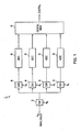
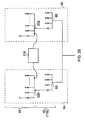
- FIG. 1 is a schematic diagram of a time-interleaved ADC 1 which may be considered generally equivalent to the known examples cited above.
- ADC 1 comprises a first sample-and-hold (S/H) circuit 2, four second S/H circuits 4, four N-bit ADCs 6 and a digital multiplexer 8.
- the first S/H circuit 2 is controlled by clock ⁇ 0 and the second S/H circuits 4 are controlled by clocks ⁇ 1 to ⁇ 4 .
- Clock ⁇ 0 is four times as fast as clocks ⁇ 1 to ⁇ 4 and clocks ⁇ 1 to ⁇ 4 are delayed relative to one another by the period of clock ⁇ 0 .
- the ADCs 6 receive samples of the input signal V IN sampled at the rate of clock ⁇ 0 in turn, so that the samples received by one ADC 6 are time-interleaved with samples received by the other ADCs 6.
- the benefit of this approach is that the four ADCs 6 can operate at a quarter of the rate of the input sampling frequency.
- the digital outputs of the ADCs 6 are multiplexed together in the digital multiplexer 8 and output as a digital signal representative of the original analogue input signal V N input to the first S/H circuit 2.
- the first S/H circuit 2 is critical (because of the frequency at which it must operate), whereas it is possible to tolerate considerable jitter (phase noise) in the four second S/H circuits 4 because the samples have already been taken at that point.
- the first S/H circuit 2 is sometimes realised off-silicon for improved performance, for example using GaAs technology.
- FIG. 1 is a schematic diagram of a time-interleaved ADC 10, which may be considered generally equivalent to the ADC disclosed in this ISSCC paper.
- the ADC 10 comprises four track-and-hold (T/H) circuits, four ADC banks 14, four demultiplexers 16, and a digital multiplexer 18.
- the overall architecture of the ADC 10 is comparable to that of ADC 1. In this way, the T/H circuits 12 operate in a time-interleaved fashion and at a quarter of the overall sampling frequency.
- ADC banks 14 are employed to convert the received samples into digital signals.
- ADC banks 14 may each comprise a plurality of time-interleaved sub-ADC circuits so as to enable those ADC circuits to operate at a yet slower rate than the T/H circuits 12, thereby demultiplexing each of the incoming signals into a plurality of output signals. Further demultiplexing may be carried out by demultiplexers 16. The digital outputs of the demultiplexers 16 are finally multiplexed together in the digital multiplexer 18 and output as a digital signal representative of the original analogue input signal V IN input to the T/H circuits 12.
- the existing architecture for an ultra-high-speed ADC such as ADC 10 of Figure 2 is an array of interleaved T/H circuits to take initial samples, followed by demultiplexing/sample-and-hold circuits which drive an array of low-speed sub-ADCs.
- This existing ADC circuitry is voltage-mode circuitry.
- a further problem is in achieving enough speed and linearity out of the front end T/H circuits, because these need to have very high bandwidth and low distortion.
- the issue is not just static linearity but also dynamic linearity in the sampling switches, because any signal-dependent switching delay introduces distortion on high-frequency input signals.
- the T/H sampling times need to be interleaved to within 0.1 ps accuracy of the ideal sample instance. This is impossible to do by design, so calibration is needed. However, the times cannot be measured directly with enough accuracy, e.g. by measuring clock-delay differences, so a calibration signal generally needs to be applied to enable the timing to be tuned (in very small steps) by minimizing FFT spurs. Even if this can be done, generating and distributing the multiple high-speed sampling clocks and providing fine-delay time adjustments is also difficult and consumes a lot of power.
- ENOB Effective Number of Bits
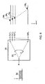
- FIG. 3 is a schematic diagram of circuitry 20 which may be employed in T/H circuits 12 of ADC 10.
- Circuitry 20 comprises a resistance 21, a transistor 22, a clock buffer 24, a signal buffer 26, and a capacitor 28.
- an analogue input voltage V IN is sampled by being gated through the transistor 22 under control of a clock signal CLK, and this sampled voltage is temporarily stored on capacitor 28 before being employed by the rest of the circuitry via buffer 26.
- a desire to operate such circuitry at a high sample rate places considerable pressure on its operation.
- the width of the clock pulses may need to be in the order of 17 ps (as indicated in Figure 3 ).
- Such fast operation also necessitates a small transistor 22 (e.g. having a gate area of less than 1 square micron), and a small capacitor 28 (e.g. having a capacitance C in the order of a few fF).
- a small transistor 22 e.g. having a gate area of less than 1 square micron
- a small capacitor 28 e.g. having a capacitance C in the order of a few fF.
- resistance 21 is generally provided to give a desired input impedance (e.g. 50 ⁇ ), and to maintain good input matching the impedance of the capacitor 28 must be much higher (e.g. 10 times) than that of the resistance 21 at the frequency of interest.
- the capacitor 28 may need to have a capacitance in the region of 16fF. At this tiny size, mismatches between the capacitors 28 of the T/H circuits can become very significant.
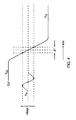
- FIG 4 is an enlarged diagram of a clock signal as it falls from its high level V DD (digital "1") to its low level V SS (digital "0"). Also shown in Figure 4 is an example input signal V IN fluctuating between maximum and minimum signal values. Although the signals in Figure 4 are not shown to scale, it will be appreciated that over the range of possible input values of the signal V IN (the maximum, middle-point and minimum values are indicated by black dots), there will be a corresponding range in values of the clock signal CLK at which the transistor 22 will switch (again, the corresponding maximum, middle and minimum such values are indicated by black dots).
- FIG. 5 is a diagram useful for further understanding the effect of such slew-rate-related and input-dependent timing errors.
- the clock signal CLK is shown as a perfect sinewave, together with a schematic indication of the clock skew on the falling edges thereof (the falling edge is assumed to be critical and, for simplicity, slew on the rising edge is not indicated).
- Figure 6 is a frequency-response diagram indicating the effects of gain mismatch G and roll-off mismatch R. Such mismatches can mean that the overall frequency response of the ADC is unpredictable.
- Figure 7 shows, in its upper half, an example ideal output FFT trace given an overall ADC sampling frequency of 56 GHz and therefore an overall ADC Nyquist frequency of 28 GHz.
- four-way sampler interleaving is assumed, with each sampler operating at a sampling frequency of 14 GHz, i.e. one quarter of 56 GHz.
- a test signal at 1 GHz is assumed to be applied to the input of the ADC in the absence of any other signal. Accordingly, a trace at 1 GHz is seen in the upper graph of Figure 7 , together with images thereof about the 14, 28, 42 and 56 GHz frequencies, as would be expected.
- Calibration can thus theoretically be performed by applying the test signal and carrying out calibration to achieve the desired frequency response.
- FFT processing is costly in terms of processing time, power consumption and complexity.
- the sample circuits do not receive signals with a simple frequency response as in the upper graph for Figure 7 . Instead, an input signal during operation will have a frequency spectrum as shown in the lower graph of Figure 7 . Performing calibration during operation could thus be prohibitively complex, forcing calibration to be carried out whilst the ADC is off-line. It is undesirable to need to take an ADC (for example in use in an Ethernet connection) off-line to perform calibration.
- EP-A1-1729420 discloses a time-interleaved analog-to-digital converter which stores in a correction information memory correction information required to correct an error between signals output by a plurality of N analog-to-digital converters in advance.
- a correction information calculating unit carries out a spectrum analysis relevant to analog-to-digital converted signals output by the plurality of N analog-to-digital converters in response to the calibration signal, thereby obtaining an amplitude and a phase of a plurality of signal components, newly obtaining the correction information, based on the amplitude and phase, and updating contents of the correction information memory in accordance with newly obtained correction information.
- US-A1-2005/0285770 discloses a high-speed current mode Analog to Digital Converter.
- the device processes an analog signal through a plurality of successive approximation ADC sub circuits cooperatively arranged to operate in parallel, time-interleaved fashion.
- the ADC sub circuits operate in current mode rather than voltage mode.
- US-A-5121121 discloses a high speed analog to digital converter system which employs a set of ACT/HACT (acoustic charge transport/hetero-junction acoustic charge transport) devices in parallel to buffer a high speed data sampling rate to the processing rate of the analog to digital converters employed. Calibration is maintained by periodic comparison of the results of the same input data.
- ACT/HACT acoustic charge transport/hetero-junction acoustic charge transport
- EP-A2-0540160 discloses a high-speed switching tree with input sampling pluses of constant frequency and means for varying the effective sampling rate.
- sampling and analogue-to-digital conversion circuits are desirable to solve one or more of the above-mentioned problems. It is desirable to provide sampling and analogue-to-digital conversion circuits, methods and techniques which enable one or more of improved distortion performance, reduced power consumption, reduced circuit size, and increased sampling rate.
- Embodiments of the present invention carry out sampling based upon currents, i.e. in the current domain. That is, in embodiments of the present invention, any information content stored in the signals is represented by the current level of those signals.
- current is the independent variable and voltage is dependent on the current; current is the cause and voltage is the effect.
- Such embodiments may be incorporated into, or employed in conjunction with, voltage-mode circuitry.
- current-mode circuitry as an arrangement for sampling a current signal, the circuitry comprising: a first node configured to have the current signal applied thereto; X second nodes conductively connectable to said first node along respective paths; and steering means for controlling such connections between the first node and the second nodes so that different packets of charge making up said current signal are steered along different said paths over time, wherein: X is an integer greater than or equal to 3; and the steering means comprises: control-signal generating means configured to generate X time-interleaved sinusoidal control signals; and switching means distributed along said paths and configured to carry out such control in dependence upon the X sinusoidal control signals.
- the use of such control signals may mean that the circuitry is difficult if not impossible to use at high frequency (e.g. at 10 GHz+).
- the X time-interleaved control signals are sinusoidal control signals.
- each control signal itself having a shape typical of a 50 % duty cycle (as is naturally true of sinusoidal signals).
- X 4 it becomes possible to employ 4 time-interleaved sinusoidal control signals, each having a 50 % duty cycle, to form 25 % duty-cycle pulses to control the four paths.
- the sinusoidal control signals the pressures on control-signal generation are relaxed, which is particularly advantageous when considering high-frequency operation. At a particular frequency of operation (e.g.
- a square-wave-type switched logic-level clock signal requires much higher frequency components than the sinusoidal control signals of the present aspect.
- a sinusoidal signal e.g. a raised cosine signal
- the control signals may be raised generally cosine signals.
- the shape of the signals may only need to be close to that of a perfect raised cosine signal in the upper part of the signals.
- the control signals may be substantially evenly time-interleaved relative to one another.
- X may equal 4. This may, for example, enable ease of compatibility with a quadrature VCO (a convenient generator of the control signals).
- the steering means may be configured such that each of the X paths is controlled by a different one of said X control signals.
- the steering means may be configured such that each of the X paths is substantially conductive when its control signal is at or around its maximum value, and is substantially non-conductive when its control signal is at or around its minimum value.
- the steering means may be configured such that when two of said control signals have the same value their corresponding paths have substantially the same level of conductivity.
- the switching means may comprise a transistor per path, and, for each path, the transistor concerned may be connected such that its channel forms part of that path and such that it is controlled by the control signal for that path. This may provide a convenient way to control the conductivity of the paths.
- the transistors may be MOSFETs having gate terminals, and, for each path, the gate terminal of the transistor concerned may be connected to receive the control signal for that path.
- the circuitry may further comprise an input node operable to receive an input voltage signal, and conversion means connected between the input node and the first node for converting the input voltage signal into the current signal, the conversion means being configured as passive circuitry comprising a resistance for performing the conversion. This may advantageously enable the circuitry to be supplied a voltage signal (which is a more convenient input signal), despite it operating in current mode.
- transconductance stage i.e. an active V-I conversion circuit
- a transconductance stage can be useful for providing a true V-I conversion, for example even if there is voltage ripple at the node to which the current signal is to be applied.
- the input impedance of such a transconductance stage tends to be capacitive (transconductor gate), and thus has a bandwidth limit in its operation.
- the use of such a transconductance can thus be highly problematic at high frequency (e.g. at 10 GHz+). At high frequency, a transconductance stage can become a significant noise and distortion contributor, and it can become very difficult to achieve satisfactory input matching.
- a resistance is provided between the input node and the first node as part of passive conversion means, to convert the input voltage signal to the current signal.
- passive conversion means may be configured to have a resistive input impedance, and thus the passive V-I conversion stage of the present aspect may be employed at very high frequencies without contributing significant noise or distortion, as constant input impedance can be achieved.
- voltage ripple at the first node is small enough to still enable a sufficiently high degree of linearity to be achieved.
- the conversion means may comprise a resistor network having the resistance and configured such that the input node has substantially constant input impedance over frequency.
- the first node may have a capacitive input impedance, for example due to parasitic capacitance on that node, and the network may comprise an inductance configured to compensate for the capacitive input impedance at the first node.
- the network may be configured such that an effect of a voltage fluctuation at said first node on conversion of the input voltage signal into the current signal is scaled down.
- the network may have a potential-divider configuration to perform such scaling down.
- the circuitry may comprise means for generating sample values based upon a characteristic of respective such charge packets passing through said second nodes, the sample values being indicative of values of said current signal corresponding to the charge packets concerned.
- a characteristic may, for example, be a peak value of the packets or an area of (i.e. an amount of charge making up) the packets.
- sample values may, for example, be digital sample values, which may be output to a digital signal processor (DSP), or other computing device.
- DSP digital signal processor
- the circuitry may comprise calibrating means operable to combine sample values from one or more of said second nodes to provide one or more combined sample values, and to calibrate operation of the circuitry in dependence upon said combined sample value(s).
- a combination e.g. an average
- the current signal is carrying an information signal such as a typical data signal whose value is changing (pseudo-randomly) over time. This also assumes that the circuitry is operating correctly.
- any differences between the combinations of sample values as mentioned above, or between a combination and a reference value may be symptomatic of errors in the operation of the circuitry, and such differences may advantageously be employed to control operation of the circuitry to reduce or eliminate such errors (i.e. to calibrate operation of the circuitry).
- the calibration may be performed whilst the circuitry is in active use, i.e. without taking it "off-stream” or “off-line” to perform the calibration.
- the calibration means may be operable to combine sample values for a said second node over time to create a combined sample value for that node, and to calibrate operation of the circuitry in dependence upon a comparison between that combined sample value and a reference value.
- Such combination may, for example, be a summation or an averaging combination.
- the calibration means may be operable to combine sample values for one said second node over time to create a combined sample value for that node, to combine sample values for another said second node over time to create a combined sample value for that other node, and to calibrate operation of the circuitry in dependence upon a comparison between those combined sample values.
- the calibration means may be operable, for each said second node, to combine sample values for that second node over time to create a combined sample value, and to calibrate operation of the circuitry in dependence upon a comparison between those combined sample values.
- Such comparisons may, for example, comprise looking for differences between said combined sample values, and looking at the relationships between those differences for different combinations of said second nodes.
- the calibration means may be operable to influence operation of the control-signal generating means and/or the switching means so as to perform such calibration.
- the calibration means may be operable to control the phase and/or magnitude of the control signals so as to perform said calibration.
- the steering means is configured such that the conductive connection of each said second node to the first node is controlled by its said control signal; the calibration means is operable to combine sample values for one candidate said second node over time to provide a combined sample value for that node, and to combine sample values for another candidate said second node over time to provide a combined sample value for that other node; and the calibration means is operable to control the phase and/or magnitude of the control signal for one or both of those candidate nodes to compensate for any difference between the combined sample values for those candidate nodes.
- the calibration means may be operable to control a dependency of said switching means on said control signals so as to perform said calibration.
- the switching means comprises a transistor per path; for each path, the transistor concerned is connected such that its channel forms part of that path and such that it is controlled by the control signal for the second node of that path; the calibration means is operable to combine sample values for one candidate said second node over time to provide a combined sample value for that node, and to combine sample values for another candidate said second node over time to provide a combined sample value for that other node; and the calibration means is operable to control a gate and/or bulk voltage for the transistor along the path for one or both of those candidate nodes to compensate for any difference between the combined sample values for those candidate nodes.
- the circuitry may comprise calibrating means operable analyse the or some of the sample values and to calibrate operation of the circuitry in dependence upon such analysis.
- control signals for use by switching means tend to be clock signals with fast clock edges, for example switched logic-level clock signals such as square waves.
- switching operations of the switching means are desensitised or shielded from the effects of mismatches between different switches of the switching means and to mismatches between different control signals used to control the switching means.
- a sinusoidal signal changes very slowly over time from its maximum to its minimum. That is, for a control signal having a particular fundamental frequency, a sinusoidal signal has a low slew rate and is the only signal that only has content at the fundamental frequency.
- sinusoidal signals it may be possible to maximise the gain from a change in mismatch to a change in the output sample value.
- This sensitivity may advantageously be employed to calibrate,operation of the circuitry to compensate for the mismatches. That is, it may be possible to analyse the sample values and calibrate operation based on the analysis.
- the circuitry may be configured to have a tree structure, wherein: the first node is a root node of the tree structure; the second nodes are first-tier nodes of the tree structure each of which is conductively connectable directly to the root node; the circuitry further comprises a plurality of subsequent-tier nodes of the tree structure per first-tier node, each of which is conductively connectable indirectly to the root node along a respective path via its said first-tier node; and the steering means is operable to control such connections between the root node and the subsequent-tier nodes so that different packets of charge making up said current signal are steered along different said paths over time.
- nodes in a tree structure having a root node, first-tier nodes, and subsequent-tier-nodes per first-tier-node, with switches making up the switching means distributed between the nodes along the paths
- the specifications for the switching performed it is possible to allow the specifications for the switching performed to become successively more relaxed from tier to subsequent tier. For example, assuming that the paths from the root node to the first-tier nodes are cycled through (for carrying packets) in an order or sequence, and assuming that there are X first tier-nodes, then the rate at which packets pass through a first-tier node is 1/X the rate at which packets pass through the root node.
- the rate at which packets pass through a second-tier node is 1/N the rate which packets pass through its first-tier node, and 1/(X.N) the rate at which packets through the root node.
- the steering means is operable to employ said sinusoidal control signals to control connections between the root node and the first-tier nodes;
- the control-signal generating means is operable to generate a plurality of time-interleaved switched-logic control signals; and the steering means is operable to employ the switched-logic control signals to control connections between the first-tier nodes and the subsequent-tier nodes.
- the control signals used to control connections between the first-tier of nodes and the subsequent-tier of nodes may have larger peak-to-peak voltages and/or longer on-times than that of the control signals used to control connections between the root node and the first-tier of nodes.
- the generating means may be operable to generate sample values based upon a characteristic of respective such charge packets passing through said subsequent-tier nodes, the sample values being indicative of values of said current signal corresponding to the charge packets concerned.
- the circuitry may comprise reset means connected to a said node other than the first node, and operable, during a period between packets for that node, to tend to bring a voltage potential of that node to a predetermined value.
- the reset means may be operable to cause the voltage potential of that node to return to the same value between successive packets for that node.
- the circuitry may comprise a plurality of said reset means each for a different such node other than the first node.
- The may be a said reset means per each such node other than the first node.
- the value that the voltage potential of each such node is caused to return to may be different for each node, or substantially the same for each node.
- the circuitry may be configured for sampling first and second complementary said current signals.
- the circuitry comprises first and second complementary circuit portions, the first portion for sampling the first current signal and the second portion for sampling the second current signal.
- Each such portion may comprise such a first node, second nodes and steering means, and the circuitry may further comprise reset means connected to at least one of a said second node of the first portion and the complementary node of the second portion, and operable, during a period between packets for that pair of complementary nodes, to tend to bring a difference in voltage potential between those two nodes to a predetermined value.
- the reset means may be connected to both nodes of the pair of complementary nodes.
- the reset means may be operable to connect the or both of the nodes of the pair of complementary nodes to (for example, via a capacitor) a reference potential, e.g. a ground supply, so as to tend to bring the difference in potential to a predetermined value.
- the reset means may be operable to bring the nodes of the pair of complementary nodes to the same potential as one another.
- the reset means may be connected between the pair of complementary nodes, and may be operable to connect those nodes together so as to bring those nodes to the same potential as one another.
- the reset means may be operable to cause a voltage potential of the or both (each) of the nodes of the pair of complementary nodes to return to the same value between successive packets. There may be provided a plurality of such reset means each for a different such pair of complementary nodes.
- Each portion may comprise generating means for generating sample values based upon a characteristic of respective such charge packets passing through the second nodes of that portion, the sample values being indicative of values of the current signal of that portion corresponding to the charge packets concerned.
- the circuitry may be configured for sampling first and second complementary said current signals.
- the circuitry may comprise first and second complementary circuit portions, the first portion for sampling the first current signal and the second portion for sampling the second current signal.
- each said portion comprises such a first node, second nodes and steering means, each said portion is configured in a tree structure, and, for each said portion, the first node is a root node of the tree structure, the second nodes are first-tier nodes of the tree structure each of which is conductively connectable directly to the root node of that portion, and that portion further comprises a plurality of subsequent-tier nodes of its tree structure per first-tier node, each of which is conductively connectable indirectly to the root node of that portion along a respective path via its said first-tier node.
- the steering means may be operable to control such connections between the root node and the subsequent-tier nodes so that different packets of charge making up said current signal are steered along different said paths over time.
- the circuitry may further comprise reset means connected to at least one of a said first or subsequent-tier node of the first portion and the complementary node of the second portion, and operable, during a period between packets for that pair of complementary nodes, to tend to bring a difference in potential between those two nodes to a predetermined value.
- the reset means may be connected to both nodes of the pair of complementary nodes.
- the reset means may be operable to connect the or both of the nodes of the pair of complementary nodes to (for example, via a capacitor) a reference potential, e.g. a ground supply, so as to tend to bring the difference in potential to a predetermined value.
- the reset means may be operable to bring the nodes of the pair of complementary nodes to the same potential as one another.
- the reset means may be connected between the pair of complementary nodes, and may be operable to connect those nodes together so as to bring those nodes to the same potential as one another.
- the reset means may be operable to cause a voltage potential of the or both (each) of the nodes of the pair of complementary nodes to return to the same value between successive packets. There may be provided a plurality of such reset means each for a different such pair of complementary nodes.
- the circuitry may comprise generating means for generating sample values based upon a characteristic of respective such charge packets passing through the subsequent-tier nodes of that portion, the sample values being indicative of values of the current signal of that portion corresponding to the charge packets concerned.
- current-mode circuitry as another arrangement for sampling a current signal, the circuitry comprising: a first node configured to have the current signal applied thereto; a plurality of second nodes conductively connectable to said first node along respective paths; steering means for controlling such connections between the first node and the second nodes so that different packets of charge making up said current signal are steered along different said paths over time; generating means for generating sample values based upon a characteristic of respective such charge packets passing through said second nodes, the sample values being indicative of values of said current signal corresponding to the charge packets concerned; and calibrating means operable to combine sample values from one or more of said second nodes to provide one or more combined sample values, and to calibrate operation of the circuitry in dependence upon said combined sample value(s).
- Such combination may be, for example, through summation or averaging.
- a combination e.g. an average
- the current signal is carrying an information signal such as a typical data signal whose value is changing (pseudo-randomly) over time. This also assumes that the circuitry is operating correctly.
- any differences between the combinations of sample values as mentioned above, or between a combination and a reference value may be symptomatic of errors in the operation of the circuitry, and such differences may advantageously be employed to control operation of the circuitry to reduce or eliminate such errors (i.e. to calibrate operation of the circuitry).
- the calibration may be performed whilst the circuitry is in active use, i.e. without taking it "off-stream" to perform the calibration.
- the calibration means may be operable to combine sample values for a said second node over time to create a combined sample value for that node, and to calibrate operation of the circuitry in dependence upon a comparison between that combined sample value and a reference value.
- the calibration means may be operable to combine sample values for one said second node over time to create a combined sample value for that node, and to combine sample values for another said second node over time to create a combined sample value for that other node, and to calibrate operation of the circuitry in dependence upon a comparison between those combined sample values.
- the calibration means may be operable, for each said second node, to combine sample values for that second node over time to create a combined sample value, and to calibrate operation of the circuitry in dependence upon a comparison between those combined sample values.
- Such comparisons may, for example, comprise looking for differences between said combined sample values, and looking at the relationships between those differences for different combinations of said second nodes.
- the steering means may comprise: control-signal generating means configured to generate a set of time-interleaved control signals, one for each said second node; and switching means distributed along said paths and configured to carry out such control of the connections in dependence upon the control signals.
- the calibration means may be operable to influence operation of the control-signal generating means and/or the switching means so as to perform such calibration.
- the calibration means may be operable to control the phase and/or magnitude of the control signals so as to perform said calibration.
- the steering means is configured such that the conductive connection of each said second node to the first node is controlled by its said control signal;
- the calibration means is operable to combine sample values for one candidate said second node over time to provide a combined sample value for that node, and to combine sample values for another candidate said second node over time to provide a combined sample value for that other node;
- the calibration means is operable to control the phase and/or magnitude of the control signal for one or both of those candidate nodes to compensate for any difference between the combined sample values for those candidate nodes.
- the calibration means may be operable to control a dependency of said switching means on said control signals so as to perform said calibration.
- the switching means comprises a transistor per path; for each path, the transistor concerned is connected such that its channel forms part of that path and such that it is controlled by the control signal for the second node of that path;
- the calibration means is operable to combine sample values for one candidate said second node over time to provide a combined sample value for that node, and to combine sample values for another candidate said second node over time to provide a combined sample value for that other node;
- the calibration means is operable to control a gate and/or bulk voltage for the transistor along the path for one or both of those candidate nodes to compensate for any difference between the combined sample values for those candidate nodes.
- current-mode circuitry as another arrangement for sampling a current signal, the circuitry comprising: a first node configured to have the current signal applied thereto; a plurality of second nodes conductively connectable to said first node along respective paths; steering means for controlling such connections between the first node and the second nodes so that different packets of charge making up said current signal are steered along different said paths over time; and generating means for generating sample values based upon a characteristic of respective such charge packets passing through said second nodes, the sample values being indicative of values of said current signal corresponding to the charge packets concerned, wherein: the steering means comprises control-signal generating means configured to generate substantially sinusoidal control signals, and switching means distributed along said paths and configured to carry out such control in dependence upon the sinusoidal control signals; and the circuitry further comprises calibrating means operable analyse the or some of the sample values and to calibrate operation of the circuitry in dependence upon such analysis.
- control signals for use by switching means tend to be clock signals with fast clock edges, for example switched logic-level clock signals such as square waves.
- switching operations of the switching means are desensitised or shielded from the effects of mismatches between different switches of the switching means and to mismatches between different control signals used to control the switching means.
- arrangements disclosed herein employ sinusoidal control signals.
- the magnitude of a sinusoidal signal changes very slowly over time from its maximum to its minimum. That is, for a control signal having a particular fundamental frequency, a sinusoidal signal has a low slew rate and is the only signal that only has content at the fundamental frequency.
- sinusoidal signals it is possible to maximise the sensitivity of the switching operations of the switching means to mismatches between different switches of the switching means and to mismatches between different control signals used to control the switching means.
- This sensitivity may advantageously be employed to calibrate operation of the circuitry to compensate for the mismatches. That is, it is possible to analyse the sample values and calibrate operation based on the analysis.
- the calibration means may be operable to influence operation of the control-signal generating means and/or the switching means so as to perform such calibration, as mentioned above.
- current-mode circuitry as another arrangement for sampling a current signal, the circuitry comprising: a root node configured to have the current signal applied thereto; a plurality of first-tier nodes each of which is conductively connectable directly to the root node; a plurality of subsequent-tier nodes per first-tier node, each of which is conductively connectable indirectly to the root node along a respective path via its said first-tier node; and steering means for controlling such connections between the root node and the subsequent-tier nodes so that different packets of charge making up said current signal are steered along different said paths over time.
- nodes in a tree structure having a root node, first-tier nodes, and subsequent-tier-nodes per first-tier-node, with switches making up the switching means distributed between the nodes along the paths
- the specifications for the switching performed may become successively more relaxed from tier to subsequent tier. For example, assuming that the paths from the root node to the first-tier nodes are cycled through (for carrying packets) in an order or sequence, and assuming that there are X first tier-nodes, then the rate at which packets pass through a first-tier node is 1/X the rate at which packets pass through the root node.
- the rate at which packets pass through a second-tier node is 1/N the rate which packets pass through its first-tier node, and 1/(X.N) the rate at which packets through the root node.
- the steering means may be operable to employ sinusoidal control signals to control connections between the root node and the first-tier nodes, and switched-logic control signals to control connections between the first-tier nodes and the subsequent-tier nodes.
- the control signals used to control connections between the first-tier of nodes and the subsequent-tier of nodes may have larger peak-to-peak voltages and/or longer on-times than that of the control signals used to control connections between the root node and the first-tier of nodes.
- Such circuitry may further comprise generating means operable to generate sample values based upon a characteristic of respective such charge packets passing through said subsequent-tier nodes, the sample values being indicative of values of said current signal corresponding to the charge packets concerned.
- current-mode circuitry as another arrangement for sampling a current signal, the circuitry comprising: a first node configured to have the current signal applied thereto; a plurality of second nodes conductively connectable to said first node along respective paths; steering means for controlling such connections between the first node and the second nodes so that different packets of charge making up said current signal are steered along different said paths over time; and reset means connected to a said second node, and operable, during a period between packets for that node, to tend to bring a voltage potential of that node to a predetermined value.
- the reset means may be operable to cause the voltage potential of that second node to return to the same value between successive packets for that node.
- the circuitry may comprise a plurality of such reset means each for a different such second node. There may be provided such a reset means per second node.
- current-mode circuitry as another arrangement for sampling first and second complementary current signals, the circuitry comprising: first and second complementary circuitry portions, the first portion for sampling the first current signal and the second portion for sampling the second current signal, wherein each said portion comprises: a first node configured to have the current signal for that portion applied thereto; a plurality of second nodes conductively connectable to the first node of that portion along respective paths; and steering means for controlling such connections between the first node and the second nodes of that portion so that different packets of charge making up the current signal of that portion are steered along different said paths of that portion over time; and reset means connected to at least one of a said second node of the first portion and the complementary node of the second portion, and operable, during a period between packets for that pair of complementary nodes, to tend to bring a difference in voltage potential between those two nodes to a predetermined value.
- the reset means may be connected to both nodes of the pair of complementary nodes.
- the reset means may be operable to connect the or both of the nodes of the pair of complementary nodes to a reference potential so as to tend to bring the difference in potential to a predetermined value.
- the reset means may be operable to bring the nodes of the pair of complementary nodes to the same potential as one another.
- the reset means may be connected between the pair of complementary nodes, and may be operable to connect those nodes together so as to bring those nodes to the same potential as one another.
- the reset means may be operable to cause a voltage potential of the or both of the nodes of the pair of complementary nodes to return to the same value between successive packets.
- There may be provided plurality of such reset means each for a different such pair of complementary nodes.
- each said portion may comprises generating means for generating sample values based upon a characteristic of respective such charge packets passing through the second nodes of that portion, the sample values being indicative of values of the current signal of that portion corresponding to the charge packets concerned.
- current-mode circuitry as another arrangement for sampling first and second complementary current signals, the circuitry comprising: first and second complementary circuitry portions, the first portion for sampling the first current signal and the second portion for sampling the second current signal, wherein each said portion comprises: a root node configured to have the current signal for that portion applied thereto; a plurality of first-tier nodes each of which is conductively connectable directly to the root node of that portion; a plurality of subsequent-tier nodes per first-tier node of that portion, each of which is conductively connectable indirectly to the root node of that portion along a respective path via its said first-tier node; and steering means for controlling such connections between the root node and the subsequent-tier nodes of that portion so that different packets of charge making up the current signal of that portion are steered along different said paths of that portion over time; and reset means connected to at least one of a said first or subsequent-tier node of the first portion and the complementary node of the second portion, and operable, during a period between
- the reset means may be connected to both nodes of the pair of complementary nodes.
- the reset means may be operable to connect the or both of the nodes of the pair of complementary nodes to a reference potential so as to tend to bring the difference in potential to a predetermined value.
- the reset means may be operable to bring the nodes of the pair of complementary nodes to the same potential as one another.
- the reset means may be connected between said pair of complementary nodes, and may be operable to connect those nodes together so as to bring those nodes to the same potential as one another.
- the reset means may be operable to cause a voltage potential of the or both of the nodes of the pair of complementary nodes to return to the same value between successive packets.
- There may be provided a plurality of such reset means each for a different such pair of complementary nodes.
- each said portion may comprise: generating means for generating sample values based upon a characteristic of respective such charge packets passing through the subsequent-tier nodes of that portion, the sample values being indicative of values of the current signal of that portion corresponding to the charge packets concerned.
- a method of sampling a current signal in current-mode circuitry comprising: controlling such connections between the first node and the second nodes in dependence upon X time-interleaved sinusoidal control signals so that different packets of charge making up said current signal are steered along different said paths over time, wherein: X is an integer greater than or equal to 3.
- a method of sampling a current signal in current-mode circuitry comprising: controlling such connections between the first node and the second nodes so that different packets of charge making up said current signal are steered along different said paths over time; generating sample values based upon a characteristic of respective such charge packets passing through said second nodes, the sample values being indicative of values of said current signal corresponding to the charge packets concerned; combining sample values from one or more of said second nodes to provide one or more combined sample values; and calibrating operation of the circuitry in dependence upon said combined sample value(s).
- a method of sampling a current signal in current-mode circuitry comprising: generating substantially sinusoidal control signals; controlling such connections between the first node and the second nodes in dependence upon the sinusoidal control signals so that different packets of charge making up said current signal are steered along different said paths over time; generating sample values based upon a characteristic of respective such charge packets passing through said second nodes, the sample values being indicative of values of said current signal corresponding to the charge packets concerned; analysing the or some of the sample values; and calibrating operation of the circuitry in dependence upon such analysis.
- a method of sampling a current signal in current-mode circuitry the circuitry having a root node configured to have the current signal applied thereto, a plurality of first-tier nodes each of which is conductively connectable directly to the root node, and a plurality of subsequent-tier nodes per first-tier node, each of which is conductively connectable indirectly to the root node along a respective path via its said first-tier node, the method comprising: controlling such connections between the root node and the subsequent-tier nodes so that different packets of charge making up said current signal are steered along different said paths over time.
- a method of sampling first and second complementary current signals in current-mode circuitry the circuitry having first and second complementary circuitry portions, the first portion for sampling the first current signal and the second portion for sampling the second current signal, wherein each said portion comprises a first node configured to have the current signal for that portion applied thereto and a plurality of second nodes conductively connectable to the first node of that portion along respective paths, the method comprising: for each said portion, controlling such connections between the first node and the second nodes of that portion so that different packets of charge making up the current signal of that portion are steered along different said paths of that portion over time; and for at least one of a said second node of the first portion and the complementary node of the second portion, and during a period between packets for that pair of complementary nodes, tending to bring a difference in voltage potential between those two nodes to a predetermined value.
- each said portion comprises a root node configured to have the current signal for that portion applied thereto, a plurality of first-tier nodes each of which is conductively connectable directly to the root node of that portion, and a plurality of subsequent-tier nodes per first-tier node of that portion, each of which is conductively connectable indirectly to the root node of that portion along a respective path via its said first-tier node, the method comprising: for each said portion, controlling such connections between the root node and the subsequent-tier nodes of that portion so that different packets of charge making up the current signal of that portion are steered along different said paths of that portion over time; and for at least one of a said first or subsequent-tier node of the first portion and the complementary node of the second portion, and during a period between packet
- a method of sampling a current signal in current-mode circuitry comprising: controlling such connections between the first node and the second nodes so that different packets of charge making up said current signal are steered along different said paths over time; and for a said second node, and during a period between packets for that node, tending to bring a voltage potential of that node to a predetermined value.
- circuitry aspects/arrangements apply equally to methods disclosed herein, and vice versa.
- Features of one circuitry aspect/arrangement such as those features specified as optional features, may be provided in combination with features of the other circuitry aspects/arrangements.
- the present invention extends to IC chips as mentioned above, circuit boards comprising such IC chips, and communication networks (for example, internet fiber-optic networks and wireless networks) and network equipment of such networks, comprising such circuit boards.
- communication networks for example, internet fiber-optic networks and wireless networks
- ADC circuitry Much of the previously-considered ADC architectures, as described with reference to Figures 1 to 7 above, carry out sampling and demultiplexing based upon voltages, i.e. in the voltage domain. That is, in such architectures, any information content stored in the signals is represented by the voltage level of those signals. In the operation of such circuitry, voltage is the independent variable and current is dependent on the voltage. Put another way, voltage is the cause and current is the effect. Such ADC circuitry is thus considered voltage-mode circuitry. In contrast, embodiments of the present invention carry out sampling and demultiplexing based upon currents, i.e. in the current domain. That is, in embodiments of the present invention, any information content stored in the signals is represented by the current level of those signals.
- ADC circuitry embodying the present invention may thus be considered to be current-mode circuitry, although it may of course be incorporated into, or employed in conjunction with, voltage-mode circuitry. Circuitry embodying the present invention may be provided as part or all of integrated circuitry, for example as an IC chip. The present invention may also extend to circuit boards comprising such IC chips.
- an embodiment of the present invention takes a current as the input signal (i.e. a signal whose current magnitude carries information content), and splits that current into n time-interleaved pulse streams, each at 1/n the overall sampling rate, using an n-phase sinewave clock.
- FIG. 8 is a schematic diagram of sampling circuitry 30.
- Circuitry 30 has an input node IN and a plurality of associated output nodes OUT 1 to OUT n .
- the input node is adapted to receive an input signal as a current 32, the magnitude of the current 32 representing the information carried by the input signal. Accordingly, although the magnitude of the current 32 is steady in Figure 8 for simplicity, it will be understood that the magnitude could fluctuate, for example to carry a data signal.
- the circuitry 30 comprises routing (or steering) means 33 for routing the received current 32 to different said output nodes (OUT 1 to OUT n ) over time.
- routing means 33 is operable to route the current 32 to different output nodes OUT 1 to OUT n in a step-wise ordered fashion and in synchronization with a clock signal (not shown).
- the routing means 33 is operable to connect the input node IN to output node OUT 1 and then to output node OUT 2 , and so on and so forth through to output node OUT n , before returning to output node OUT 1 .
- the routing means 33 cycles through the output nodes such that the current 32 is effectively divided up on a time-wise basis into samples (or parts) 34 1 to 34 n received at the output nodes OUT 1 to OUT n , respectively.
- the routing means 33 may change its connection from one output node to the next such that no two output nodes are ever connected to the input node at the same time. Alternatively, as is true of embodiments of the present invention disclosed herein, the routing means 33 may gradually change its connection from one output node to the next such that there are periods of time when more than one output node is connected to the input node.
- Circuitry 30 may further comprise generating means (not shown) for generating output values based upon the samples or pulses 34 1 to 34 n received at the output nodes OUT 1 to OUT N , the output values being indicative of input values of parts of the input signal (current 32) corresponding to said current samples 34 1 to 34 n .
- the circuitry 30 may thus be configured to perform analogue-to-digital conversion, for example if the generating means is operable to output digital output values.
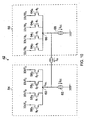
- FIG. 9 is a schematic diagram of analogue-to-digital circuitry 40 embodying the present invention.
- Circuitry 40 comprises sampler 42, voltage-controlled oscillator (VCO) 44, demultiplexers 46, ADC banks 48, digital unit 50 and calibration unit 52.
- VCO voltage-controlled oscillator
- the sampler 42 is configured to perform four-way or four-phase time-interleaving so as to split the input current I IN into four time-interleaved sample streams A to D.
- VCO 44 is a quadrature VCO operable to output four clock signals 90° out of phase with one another, for example as four raised cosine signals.
- VCO 44 may for example be a shared 14 GHz quadrature VCO to enable circuitry 40 to have an overall sample rate of 56 GS/s.
- Each of streams A to D comprises a demultiplexer 46 and an ADC bank 48 connected together in series as shown in Figure 9 .
- the sampler operates in the current mode as in previous embodiments, and, accordingly, streams A to D are effectively four time-interleaved streams of current pulses originating from (and together making up) input current I IN , each stream having a sample rate one quarter of the overall sample rate.
- each of the streams A to D may have a 14 GS/s sample rate.
- the stream of current pulses is first demultiplexed by an n-way demultiplexer 46.
- Demultiplexer 46 is a current-steering demultiplexer and this performs a similar function to sampler 42, splitting stream A into n time-interleaved streams each having a sample rate equal to 1/4n of the overall sample rate.
- the n output streams from demultiplexer 46 may each have a 14/n GS/s sample rate. If n were to be 80 or 160 for example, the output streams of demultiplexer 46 may have a 175 MS/s or 87.5 MS/s sample rate, respectively.
- circuitry 40 may be considered to comprise 320 ADC sub-units split between the four ADC banks 48.
- the four sets of n digital streams are thus input to the digital unit 50 which multiplexes those streams to produce a single digital output signal representative of the analogue input signal, current I IN .
- This notion of producing a single digital output may be true schematically, however in a practical implementation it may be preferable to output the digital output signals from the ADC banks in parallel.
- Calibration unit 52 is connected to receive a signal or signals from the digital unit 50 and, based on that signal, to determine control signals to be applied to one or more of the sampler 42, VCO 44, demultiplexers 46 and ADC banks 48. As will become apparent later, it is preferable to carry out calibration on the sampler 42, which is why the output from calibration unit 52 to the sampler 42 is shown as a solid arrow in Figure 9 , rather than as a dashed arrow.
- circuitry 40 will become apparent through consideration of Figures 10 to 27 .
- Figure 10 is a schematic circuit diagram of four-phase (i.e. multiphase) current-mode (current-steering) sampler 42.
- a single-ended input signal, current I IN is shown, it will be appreciated that a differential input signal could be employed, for example to take advantage of common-mode interference rejection. Accordingly, the sampler 42 and demultiplexers 46 and ADC banks 48 could be effectively duplicated in circuitry 40 to support such differential signaling, however such duplication is omitted from Figure 9 for simplicity.
- sampler 42 is configured to receive such a differential input current signal, modeled here as a current source I IN whose magnitude varies with the input signal.
- sampler 42 effectively has two matching (or corresponding or complementary) sections 54 and 56 for the two differential inputs. Accordingly, there is a first set of output streams IOUT A to IOUT D in section 54 and a second set of matching output streams IOUTB A to IOUTB D , where IOUTB means IOUT , and wherein IOUT A is paired with IOUTB A , IOUT B is paired with IOUTB B , and so on and so forth.
- n-channel MOSFETs 58 A to 58 D i.e. one per stream or path
- source terminals connected together at a common tail node 60.
- the aforementioned current source I IN is connected between common tail node 60 and an equivalent common tail node 66 of section 56.
- a further current source I DC 62 is connected between the common tail node 60 and ground supply, and carries a constant DC current I DC .
- the gate terminals of the four transistors 58 A to 58 D are driven by the four clock signals ⁇ 0 to ⁇ 3 , respectively, provided from the VCO 54.
- section 56 is structurally similar to section 54 and thus comprises transistors 64 A to 64 D , common tail node 66 and current source I DC 68.
- Figure 11 shows schematic waveforms for the clock signals ⁇ 0 to ⁇ 3 in the upper graph, and schematic waveforms for the corresponding output currents IOUT A to IOUT D in the lower graph.
- the clock signals ⁇ 0 to ⁇ 3 are time-interleaved raised cosine waveforms provided as four voltage waveforms from the VCO 44.
- the use of four clock signals in the present case is due to the four-way-interleaving design of ADC circuitry 40, but it will be appreciated that, in another embodiment, three or more time-interleaved clock signals could be used, for a three-or-more-way split of the input current signal.
- Clock signals ⁇ 0 to ⁇ 3 are 90° out of phase with one another, such that ⁇ 0 is at 0° phase, ⁇ 1 is at 90° phase, ⁇ 2 is at 180° phase, and ⁇ 3 is at 270° phase.
- sampling circuitry 42 under control of clock signals ⁇ 0 to ⁇ 3 , is that the output currents IOUT A to IOUT D are four trains (or streams) of current pulses, the series of pulses in each train having the same period as one of the clock signals ⁇ 0 to ⁇ 3 , and the pulses of all four trains together being time-interleaved with one another as an effective overall train of pulses at a quarter of the period of one of the clock signals (or at four times the sampling frequency of one of the clock signals).
- Figure 12 shows more waveforms for the clock signals ⁇ 0 to ⁇ 3 in the upper graph, and partial waveforms for the currents IOUT A , IOUT B and IOUT D (current IOUTc is not shown) in the lower graph, for use in better understanding the operation of sampling circuitry 42.
- clock signals ⁇ 0 to ⁇ 3 are time-interleaved raised (substantially) cosine waveforms and are 90° out of phase with one another.
- the clock signals shown are sinusoidal, but need not be strictly-perfect sinusoids. As will become apparent, in the present embodiment the shape of the waveforms is more important in the uppermost part than towards the bottom.
- clock signal ⁇ 0 is highlighted in bold in Figure 12 .
- Clock signals ⁇ 0 to ⁇ 3 control the gates of transistors 58 A to 58 D , respectively, in sampler 42. Accordingly, transistors 58 A to 58 D are turned on and then off in sequence, such that as one of them is turning off the next in sequence is turning on, and such that when one of them is turned fully on the others are substantially turned off.
- waveform ⁇ 0 is at its peak value, i.e. at V DD , and the other clock signals ⁇ 1 to ⁇ 3 are significantly below their peak value. Accordingly, transistor 58 A is fully on and transistors 58 B to 58 D are substantially off. Therefore, at the corresponding point 80, current IOUT A is equal to I TAIL and the other currents IOUT B and IOUT D (and current IOUT C not shown) are substantially equal to zero.
- waveform ⁇ 0 is rising towards its peak value but has not yet reached its peak value.
- waveform ⁇ 3 is falling from its peak value.
- clock signals ⁇ 3 and ⁇ 0 have equal values. Therefore transistors 58 D and 58 A are on to the same extent as one another, because their source terminals are connected together.
- clock signals ⁇ 1 and ⁇ 2 are also equal to one another and are sufficiently low to ensure that transistors 58 D and 58 C are off.
- each current waveform e.g. points 80, 82 and 84 for current waveform IOUT A
- the three points for each current waveform are fixed in time relative to the clock waveforms and in magnitude relative to the current I TAIL . That is, taking current IOUT A as an example, at point 80 the current is equal to I TAIL and at points 82 and 84 the current is equal to half I TAIL .
- the location of points 80, 82 and 84 is fixed relative to the clock signals ⁇ 0 to ⁇ 3 .
- currents IOUT B to IOUT D The focus on points 70, 72 and 74 demonstrates that for the present embodiment the upper part of the clock signals is important, and that the lower parts are less important (such that, for example, the precise shape of the lower parts is not strictly critical).
- the current pulses of waveforms IOUT A to IOUT D are all of the same shape, and that shape is defined by the raised cosine shape of the clock signals.
- the pulses are simply scaled up or down accordingly. This can be seen from Figure 13 , which shows waveforms for IOUT A to IOUT D as I TAIL increases and then decreases again. The peaks of the pulses follow I TAIL , and the points where two adjacent pulses have equal value (i.e. the crossing points) follow half I TAIL .
- the frequency response/roll-off is thereby defined mathematically by the cosine curve and as a result the analogue bandwidth from the input I IN to the output I OUT is very high, typically greater than 100 GHz.
- the voltage level at the tail nodes in the circuitry e.g. nodes 60 and 66 in Figure 10 ) does not fluctuate much during operation.
- the switches are nMOS switches, operated in the saturated region, with their source terminals tied together to form the tail node concerned. Thus, those switches operate as cascodes with a low input impedance and a high output impedance.
- the transistor 22 has to drive capacitor 28. There is thus a high resistance and relatively high capacitance giving a relatively low bandwidth, and the bandwidth is unpredictable because of the significant mismatch in capacitor 28.
- the nMOS switches do not have to drive a capacitor 28; they have a low on resistance and the tail nodes have a tiny parasitic capacitance (to which the tail node is insensitive as mentioned above). This gives a high bandwidth that is accurate and repeatable.
- the circuitry of the present embodiment is a fast analogue circuit carrying current pulses of a defined shape.
- the circuitry thus has a high bandwidth that is known, repeatable, accurate and constant. This known bandwidth may thus be compensated for with a filter (as mentioned below), for example digitally.
- the demultiplexers 46 operate in a similar way to the sampler 42, leading to this high-bandwidth accurate operation over the sampling and demultiplexing circuitry.
- the sampling circuitry 42 operates by genuinely steering the current I TAIL whose magnitude is dependent upon input signal I IN via the different outputs IOUT A to IOUT D .
- the input current I TAIL is not copied (in the way that voltages are copied in voltage-mode ADCs) from stage to stage (the demultiplexers 46 having a similar structure and method of operation to the sampling circuitry 42 and thus forming subsequent such stages). Instead, it is the actual current I TAIL that is steered or routed through the circuitry. All of the current I TAIL passes through to the outputs.
- the operation does not suffer from significant input-signal-dependent sampling delays.
- the voltage at common tail nodes 60 and 66 can be configured to be very stable during operation, such that it is only susceptible to around 50-70 mV ripple.
- the sampling timing is purely governed by the clock signals ⁇ 0 to ⁇ 3 as explained above (because the source terminals of the switching transistors are all tied together). Therefore, a change in I IN does not cause any signal-dependent delay, in contrast to the signal-dependent delay as explained earlier with reference to Figures 3 to 5 . Accordingly, related distortion is also obviated.
- any errors are mainly (i.e. ignoring insignificant signal-dependent errors) due to mismatches between the switching transistors (and such mismatches are dealt with later).
- sampler circuitry 42 may be driven directly without requiring an intermediate buffer such as buffer 24 in Figure 3 .
- VCO outputs tend to be sinusoidal and the present circuitry is configured to accept sinusoidal clock signals.
- Such direct driving may include intermediate AC coupling, e.g. via a capacitor.
- the gate capacitances of the transistors of the sampler circuitry 42 can be included in the VCO 44 design as being part of necessary capacitance within the VCO.
- the gate capacitances are effectively absorbed within the VCO, such that the sampler circuitry 42 operates as if there were zero gate capacitance.
- switching delays due to gate capacitances are effectively removed.
- buffers such as buffer 24 to generate square (i.e. pulsed or switched-logic) waves allows associated noise and delay mismatch to be avoided. For example, if quadature square waves were required, then four buffers with associated mismatch would be required.
- Figure 14 shows simulation results for sampler circuitry 42.
- the circuitry 42 has been configured to operate at 56 GS/s and is supplied with an input current signal I IN having the form of a 1 GHz sinewave.
- the uppermost of the four graphs shows the four clock signals ⁇ 0 to ⁇ 3 , each being a 14 GHz raised cosine signal, thereby enabling the overall desired 56 GS/s sampling rate.
- the second of the four graphs from the top shows the four output signals IOUT A to IOUT D of section 54 and the third of the four graphs shows the equivalent traces for output signals IOUTB A to IOUTB D of section 56.
- the lowermost graph shows the difference between the two components of the differential output signal, i.e. generically IOUT-IOUTB. In such differential circuitry, it is the "difference" signal that is the desired output.
- Figure 15 shows an enlarged portion of the simulation results of Figure 14 , in which the pulse shapes and clock signals are more clearly shown.
- the resulting fixed pulse shape can be clearly seen.
- the peaks of the pulses in the middle two graphs follow I TAIL and thus fluctuate around a DC level defined by the DC current sources 62 and 68.
- the circuitry component values used for the simulation were similar to those employed in the Figure 16 circuitry (described below), except that the impedances were halved, the current sources were doubled, and 25 ⁇ resistors were provided in series at the inputs VINP and VINM. This enabled the input impedance to remain on target, the voltage swings to remain the same, and the current signals to be doubled.
- the overall input 1 GHz signal can be seen as the envelope of the lower graph.
- the input signal is represented both by the peak values of the successive pulses, and by the areas under the successive pulses; because of the defined shape of the pulses, the peak values double as the areas double, and vice versa.
- ADC circuitry 40 operates in the current domain, i.e. effectively as a current-mode ADC.
- the input signal required is a current signal.
- typical signals that require use of an ADC or sampler are voltage-domain signals, in which the variable under examination is a voltage rather than a current.
- Figure 16 is a schematic circuit diagram of an example implementation 102 of sampling circuitry 42, to which it is possible to apply an input differential voltage signal.
- Implementation 102 similarly to circuitry 42, comprises two sections 54 and 56 for the so-called “plus” and “minus” components of the differential signals.
- Section 54 comprises switching transistors 58 A to 58 D connected to common tail node 60
- section 56 comprises switching transistors 64 A to 64 D connected to common tail node 66, as before.
- Implementation 102 basically works by receiving the input voltage signal and by employing resistances to passively convert the received input voltage signal into an equivalent input current signal.
- Implementation 102 therefore comprises input terminals 104 (VINP) and 106 (VINM) to receive the "plus” and “minus” components of the input voltage signal, respectively.
- Input terminals 104 and 106 are each connected to a shared terminal 108 via a resistor 110 and an inductor 112. Input terminals 104 and 106 are further each connected to their corresponding common tail nodes 60 and 66 via a resistor 114.
- Shared terminal 108 is connected via shared DC current source 116 to a reference potential whose voltage level is below that of VINO and VINM, and may indeed be negative.
- FIG. 16 An example set of resistance values are shown in Figure 16 . These values have been chosen assuming an example design objective that the input impedance looking into each of the common tail nodes 60 and 66 towards the switching transistors (sampler switches) is 50 ⁇ , and that the input impedance looking into each of the input terminals 104 and 106 is also 50 ⁇ as shown in Figure 16 . A further example aim is for the circuitry to have an analog bandwidth from VIN to IOUT of more than 100 GHz when implemented in 65 nm silicon technology.
- resistor 110 By setting resistor 110 as 100 ⁇ and resistor 114 as 50 ⁇ , it is possible to obtain an impedance Z 1 looking into the input terminals 104 and 106 towards the respective common tail nodes 60 and 66 of 100 ⁇ at DC and 50 ⁇ at high frequency (e.g. at 100 GHz), an impedance Z 2 looking into the input terminals 104 and 106 towards the shared terminal 108 of 100 ⁇ at DC and infinity at high frequency, and therefore a total input impedance Z IN at each input terminal 104, 106 of 50 ⁇ over the full bandwidth.
- the sampler switches look capacitive at around 100 GHz and are compensated by the series inductors 112 (around 100 pH) in the tail.
- An advantage of the infinite impendance Z 2 at high frequency is that shared node 108 effectively serves as an AC ground such that the operation of the circuitry is shielded from any capacitance in the shared current source 116. Put simply, the inductance 112 isolates any capacitance in the current source 116 because they compensate for one another. Put another way, because the circuit is differential and balanced, the voltage at node 108 doesn't move much, so there is no signal on node 108 and that node is insensitive to capacitance.
- a transconductance stage i.e. an active V-I conversion circuit
- a transconductance stage can, for example, be useful for providing a true V-I conversion even if there is expected voltage ripple at the node (e.g. node 60 in Figure 16 ) to which the current signal is to be applied.
- the input impedance of such an active transconductance stage has a relatively low bandwidth limit (e.g.
- the present example implementation 102 provides passive conversion means with substantially constant (i.e. resistive) input impedance over frequency (in the example above, there is provided 50 ⁇ input impedance at DC to over 100 GHz).
- the example implementation 102 enables good input matching and can be used at high frequency without being a significant noise or distortion contributor.
- the ripple at the tail nodes e.g. nodes 60 and 66 in Figure 16
- a sufficient degree of linearity may still be achieved (e.g. an ENOB of 8).
- Figure 17 is a schematic circuit diagram of parts of ADC circuitry 40 useful for understanding the structure and operation of the demultiplexers 46.
- demultiplexers 46 only the demultiplexing circuitry 46 for output IOUT A is shown. Similar circuitry may also be provided for the other seven outputs IOUT B to IOUT D , and IOUTB A to IOUTB D .
- demultiplexers 46 in the present embodiment are formed of two stages, namely stages 46A and 46B.
- the first stage 46A performs 1:N demultiplexing
- the second stage 46B performs 1:M demultiplexing.
- Stages 46A and 46B generally have the same structure as the array of sampling switches 110 of the sampling circuitry 42. That is, each stage comprises a plurality of transistors (in this case, n-channel MOSFETs) whose source terminals are connected together at a common tail node.
- transistors in this case, n-channel MOSFETs
- those pulse trains are provided at outputs IOUT A to IOUT D .
- Sampling circuitry 42 can thus be thought of as performing a 1:X demultiplexing function.
- each output from sampler 42 can be further 1:N demultiplexed by a stage 46A, and each output of a stage 46A can be further 1:M demultiplexed by a stage 46B.
- Z X x N x M.
- the present embodiment performs 1:320 demultiplexing, which leads to 320 outputs on the "plus” side 54 and a corresponding 320 outputs on the "minus" side 56.
- Figure 18 is a schematic diagram useful for understanding further the operation of demultiplexers 46.
- the uppermost trace shows a pulse train at output IOUT A of the sampling circuitry 42, and the traces below represent corresponding pulse trains of outputs IOUT A10 to IOUT A1(N-1) (only IOUT A10 to IOUT A13 are shown) of a stage 46A.
- pulse train IOUT A is effectively split up into N pulse trains each at 1/N the sample rate of pulse train IOUT A .
- the clock signals ⁇ 0 and ⁇ 3 supplied to sampling circuitry 42 are, in this embodiment, low-voltage (e.g. having 0 V to 0.8 V clock levels) raised cosine waveforms (which lead to the related advantages discussed earlier), the specifications for the clock signals applied to stages 46A and 46B of the multiplexers 46 can be somewhat relaxed in comparison. This is because by that stage the samples have already been taken, and because at successive stages the sample rate becomes much reduced. The clock performance at successive stages therefore becomes less critical. As a result, for example, the clock signals applied to stages 46A and 46B could be digital clock signals (i.e.
- the sampling and demultiplexing circuitry of the present embodiment forms a series of nodes connected together in a tree structure. This is true for both complementary parts of the circuitry, looking at, for example, Figure 16 .
- node 60 may be considered a root node of its tree structure, with the next tier of nodes having outputs IOUT A to IOUT D , and (moving to Figure 17 ) the next tier of nodes having (amongst others not shown) outputs IOUT A1020 to IOUT A102(M-1).
- the sample-rate reduction from tier to subsequent tier enables the clock specifications to be relaxed from tier to subsequent tier. Despite this relaxtion from tier to tier, because the samples are taken in the sampler circuitry (between the root and first-tier nodes), the samples can then pass through the subsequent tiers largely unaffected.
- ADC banks 48 are used to produce digital values corresponding to the areas of the respective current pulses input thereto. It is of course not essential for digital values to be output; instead, analog values could be output. Digital output values are simply a useful output format for compatibility with external digital systems, such as processors (e.g. digital signal processors, DSPs) and other computing devices.
- processors e.g. digital signal processors, DSPs
- FIG 19 is a schematic diagram useful for understanding the principle of operation of ADC banks 48. For simplicity, only one output, lOUT A1020, of demultiplexers 46 is shown, and consequently the ADC circuitry 48 shown represents only the ADC circuitry required for that particular output. Similar ADC circuitry 48 may be provided for all the outputs of the demultiplexers 46.
- ADC circuitry 48 generally takes the form of a capacitance 150.
- capacitance 150 may be variable in value, such that its value can be trimmed during calibration or during an initial setup phase.
- the voltage V OUT for a particular pulse is held across capacitance 150 until the circuitry 48 is reset by reset switch 152. Whilst the voltage V OUT for a particular pulse is held, this analog output value can be converted into a digital output value, for example using an ADC circuit employing a successive-approximation register (SAR).
- SAR successive-approximation register
- each V OUT will have its complementary V OUT , and the pair may be applied together to a differential comparator so that a single digital output for that pair is output.
- An advantage of this mode of operation is that even if delays are experienced within the demultiplexers 46, the charge in each pulse will still make it to the relevant outputs, albeit over a slightly longer period. In that case, the voltage V OUT produced from the pulse remains unaffected.
- the first pulse 154 represents a case in which minimal delay is experienced.
- the second pulse 156 represents a case in which some delay is experienced, for example due to track capacitance in the circuitry. Consequently, pulse 156 is stretched in time as compared to pulse 154.
- the area of the two pulses 154 and 156 is substantially the same, and thus the output voltage V OUT would be the same for both.
- mismatches in the capacitances 150 have less of an effect than mismatches in capacitances 28. This is because errors due to mismatches in capacitances 28 are caused at the initial sampling stage in circuitry 20 (where the number of such capacitances 28 is small), however errors due to mismatches in capacitances 150 in the present embodiment are caused at the final ADC stage (where the number of such capacitances 150 is large).
- the capacitors 28 in the Figure 3 circuitry need to be small to achieve the desired input impedance, and at such a small size the mismatch can be large.
- the example size of capacitor 28 given above was 16fF.
- the capacitances 150 may be relatively large, since they are not attached at the inputs.
- the capacitances 150 may, for example, be ten times (10X) larger than the capacitors 28.
- capacitances 150 may have a capacitance of 160fF.
- the reduction in mismatch is found to be approximately proportioned to the square root of the factor increase in area taken up in silicon (assuming silicon implementation), i.e. approximately proportional to the square root of the factor increase in size of the capacitance value. In the present embodiment, it could be expected that, for this reason, errors due to capacitance mismatches are reduced by a factor of 10 .
- FIG 20 is a schematic diagram useful for understanding a possible application of SAR - ADC (Successive Approximation Register - Analogue-to-Digital Conversion) circuitry to circuitry 48 in Figure 19 .
- Such circuitry could have a cycle of phases of the form: Reset (R); Sample (S); 1; 2; 3; 4; 5; 6; 7 and 8, as shown in Figure 20 .
- Reset R
- Sample S
- 1; 2; 3; 4; 5; 6; 7 and 8 shown in Figure 20 .
- a current pulse concerned may be converted into an output voltage V OUT , and subsequently that voltage V OUT may be turned into an 8-bit digital value over the following 8 SAR stages.
- the next Reset stage then prepares the circuitry for the next current pulse.
- calibration unit 52 is provided in ADC circuitry 40 to calibrate its operation.
- calibration unit 52 is capable of performing such calibration of the ADC circuitry 40 in use, i.e. without the need to take it "off-line".
- the operation of the calibration unit 52 relies on the principle that the sampling circuitry 42 divides up the input current into streams of current pulses, i.e. that all of the current that is sampled appears in the pulses at the output.
- the general idea is that timing errors in the VCO/sampler clocks or switches affect the areas of the current pulses, and therefore the ADC output value. More particularly, as illustrated in Figure 22 , because all the current is divided up into pulses, if one pulse is increased in area (from its expected area in an error-free environment) due to such an error, then another pulse or set of pulses must see a corresponding decrease in area because the input current is divided up into the output currents (without current being added or removed). Similarly, if one pulse is decreased in area due to an error, then another pulse or set of pulses must see a corresponding increase in area.
- the clock signals are sinusoidal (which are slow signals, in the sense of rise and fall times, in contrast to fast conventional digital switched-logic or square-wave signals), the sensitivity of the areas of the current pulses to phase or magnitude errors in the clock signals, and/or to mismatches between the sampling switches, is maximized.
- the use of sinusoidal clock signals enables the gain from ⁇ V TH (the change in threshold voltage of a sampling switch, representative of a mismatch) to ⁇ I (the change in area of a resultant current pulse caused by the change in threshold voltage) is maximized.
- ⁇ V TH the change in threshold voltage of a sampling switch, representative of a mismatch
- ⁇ I the change in area of a resultant current pulse caused by the change in threshold voltage
- Figure 23 is a partial duplication of the waveforms shown in Figure 12 .
- the lower graph shows three pulse shapes, labeled P 3 , P 0 , and P 1 which are intended to schematically represent the averaged digital output powers corresponding to the outputs of sampler circuitry 42 generated by clocks ⁇ 3 , ⁇ 0 and ⁇ 1 , respectively.
- Waveforms ⁇ 3 , ⁇ 0 and ⁇ 1 in Figure 23 represent the effective gate drives for sampler circuitry 42 which would produce equally-sized averaged digital output powers P 3 , P 0 , and P 1 .
- Effective gate drive ⁇ 0-P which could for example result from a timing error in the VCO 44.
- Effective gate drive ⁇ 0-P is intended to be a phase-shifted version of the effective gate drive ⁇ 0 resulting from such a timing error.
- the power P 3 would increase, for example by 10%
- the power P 0 would stay the same
- the power P 1 would decrease in line with the increase in P 3 , again for example by 10%. Detecting this pattern of changes in the averaged digital output powers P 3 , P 0 and P 1 could therefore indicate the presence of a timing error in VCO 44 in relation to clock ⁇ 0 .
- Figure 24 is a partial duplication of the waveforms shown in Figure 12 , as in Figure 23 . Accordingly, waveforms ⁇ 3 , ⁇ 0 , ⁇ 1 , P 3 , P 0 and P 1 in Figure 24 are identical to those in Figure 23 .
- an effective gate drive ⁇ 0-M which could for example result from a threshold voltage (V TH ) error (mismatch) in one of the sampling switches 58 A to 58 D (or 64 A to 64 D ) in sampling circuitry 42.
- Effective gate drive ⁇ 0-M is therefore intended to be a magnitude-reduced version of effective gate drive ⁇ 0 resulting from such a V TH error.
- the power P 0 would decrease, for example by 20%, and that the neighbouring powers P 3 and P 1 would increase equally in line with that decrease, for example by 10% each. Detecting this pattern of changes in the average digital output powers P 3 , P 0 and P 1 could therefore indicate the presence of such a V TH error.
- switches S 0 and S 1 are corresponding switches of a differential pair.
- the calibration may then be performed taking into account the results of this methodology.
- the bulk and/or gate voltage applied to one or both of sampling switches S 0 and S 1 could be controlled to reduce or eliminate the mismatches.
- Demultiplexers 46 are similar in structure to sampling circuitry 42 as discussed above, and therefore they are similarly susceptible to V TH mismatches. In the same way as a V TH error in a particular sampler switch (e.g. switch 58 A ) can be detected, so an error in a particular demultiplexer switch (e.g. the switch outputting signal IOUT A10 in Figure 17 ) may be detected by selecting appropriate digital outputs to average and to compare with one another. For example, an averaged digital output power could be obtained for a particular switch under investigation by combining all outputs stemming from that switch, and a corresponding output power could similarly be obtained for another switch in the same tier, and these powers (and other similar powers) could be compared as above, to calibrate the switch under investigation.
- V TH error in a particular sampler switch e.g. switch 58 A
- an error in a particular demultiplexer switch e.g. the switch outputting signal IOUT A10 in Figure 17
- an averaged digital output power could be obtained
- the calibration circuitry 52 may be used to adjust operation of the ADC circuitry 40 to compensate for those errors. Because the errors are detected by averaging real output signals, the calibration can be carried out "on-line".
- one possible technique is to directly control operation of the VCO 44 as indicated in Figure 9 , for example to adjust the phase offset between the clock signals ⁇ 0 to ⁇ 3 until a phase-error effect as in Figure 23 is eliminated.
- Another technique is to directly control operation of the switches, primarily focusing on the sampling switches in sampling circuitry 42 (since they are responsible for taking the samples), and, as a secondary measure, focusing on the switches in demultiplexers 46.
- One way to directly control operation of the switches is to control the bulk voltage applied to those switches.
- Another way is to adjust the gate voltages applied to those switches.
- the clock signals output from the VCO44 may be AC coupled (e.g. via a series capacitor) to the sampler switches, and thus the DC bias may be adjusted.
- FIG 25 is a schematic diagram of such a switch, in which a trim voltage V TRIM is applied to the body terminal.
- V TH threshold voltage
- the effect of changing the bulk voltage of a particular switch (transistor) is to change the gate-source voltage at which the transistor changes state.
- trim voltages V TRIM By applying appropriate trim voltages V TRIM to the body terminals of switches identified to be causing errors, their bulk voltages may be varied to compensate for the effects of random threshold voltage variations on their switching points.
- This technique may also be used to compensate for other mismatches, i.e. by varying operation of the transistors until the effects of those other mismatches are eliminated.
- a technique of bulk-voltage variation is disclosed in EP07113379.7 (the entire contents of which, in particular in relation to Figure 13 thereof, are incorporated herein by reference) and this technique may be applied by analogy in embodiments of the present invention.
- Calibration can accordingly be carried out "on-line” until the chosen averaged digital output powers are equal to one another.
- the pulses on average have the same area, in which case they have the same width and are thus equally spaced apart. In this way, sampling skew is removed to a first order approximation.
- Figures 26 and 27 present simulation results for a full implementation of ADC circuitry 40 configured for the sampling circuitry 42 to perform 1:4 demultiplexing and for the demultiplexers 46 to be single-stage 1:4 demultiplexers, so that the overall circuitry performs 1:16 demultiplexing.
- the output current pulses are integrated onto ADC input capacitors, and the outputs of the demultiplexers 46 are recombined to create an equivalent single ADC output signal. That single output signal is then subject to FFT processing to produce the frequency-domain results in Figure 26 .
- the uppermost trace represents a fast silicon process
- the middle trace represents a typical silicon process
- the lower trace represents a slow silicon process.
- Those three processes are also represented in the other two charts.
- the results in Figure 27 are actual time-domain signal traces from the simulation.
- the output has an ENOB (effective number of bits) of greater than 8 bits for an input signal frequency of up to 20 GHz. This was measured with a full-scale sinewave. Sampler distortion will fall with signal level.
- Figure 28 is a schematic diagram of parts of ADC circuitry 40 according to one embodiment of the present invention, incorporating a refinement.
- the circuitry in Figure 28 is presented schematically in a similar format to that in Figure 17 , except that the resistances are omitted and the switches are represented as crosses.
- only parts of the sampler circuitry 42 and demultiplexer circuitry 46 are shown, as in Figure 17 . However, both the "plus” and "minus" complementary sections 54 and 56 are shown.
- a tail node in the demultiplexer circuitry 46 of section 54 is marked with numeral 200 and the corresponding tail node in section 56 is marked with numeral 202.
- such nodes (like root tail nodes 60 and 66 in the samler circuitry 42) generally have a parasitic capacitance, and therefore a tiny (but nonetheless existent) amount of charge can be stored over those parasitic capacitances as packets or pulses of charge pass through those nodes during use.
- circuitry in Figure 28 is differential circuitry, it is not specifically the size of the individual packets of charge that is important, but more so the difference between the size of a packet of charge passing through section 54 and its corresponding complementary packet of charge passing through section 56.
- An amount of charge may be left behind over the parasitic capacitance of, for example, node 200 as a packet/pulse of charge passes through, and a different amount of charge may be similarly left behind at node 202.
- these amounts of residual charge may affect the sizes of the next pair of pulses that pass through, and thus be the cause of errors.
- the circuitry of Figure 28 comprises reset circuitry 210.
- Reset circuitry 210 takes advantage of the so-called "down time" that node pair 200 and 202 have between packets of charge.
- the equalization circuitry acts to bring each of nodes 200 and 202 to the same potential that it was at prior to the previous packet it carried. In this way, each of those nodes is returned to the same starting voltage each time before a packet passes through, so that the effect of any residual charge is the same for each packet. This is one way of aiming to keep the difference in potential between the two nodes of the pair the same from cycle to cycle.
- reset circuitry 210 may, for example, be implemented as a pair of switches (not shown), connecting their respective nodes 200 and 202 to ground via a large capacitance. Those switches may make use of an existing clock signal that is active for another node at a time when nodes 200 and 202 are intended to be inactive. In that way, nodes 200 and 202 may both be connected to ground together to return the residual charge on each of them to a starting value during the down time. By returning the residual charge on the two complimentary nodes 200 and 202 to a starting value (which may be different for each node), an error that might otherwise have impacted on the next set of pulses may be substantially prevented.
- Reset circuitry 210 may be implemented in many other ways, for example it may even be employed to connect nodes 200 and 202 together each time, to equalize the charge on those nodes.
- reset circuitry 210 may be provided for any or all pairs of complementary nodes in the tree structures of Sections 54 and 56, to reset the residual charge on them during their "down time". This includes all nodes in the tree structure right through the demultiplexer circuitry 46A through to the sub-ADC circuitry 46B & 48 (see Figure 21 ), in each case using an appropriate existing (or possibly dedicated) clock signal to activate the switches concerned during the down time for the pair of nodes concerned. This technique is unpractical between nodes 60 and 66, since they do not have "down time” in the way that the other nodes do (which can be appreciated from a comparison of Figure 13 with Figure 18 ).
Landscapes
- Engineering & Computer Science (AREA)
- Theoretical Computer Science (AREA)
- Analogue/Digital Conversion (AREA)
- Electronic Switches (AREA)
- Measurement Of Current Or Voltage (AREA)
- Semiconductor Integrated Circuits (AREA)
Claims (10)
- Circuits à mode de courant, comprenant :un premier noeud (60, 66) dans lequel un courant circulant change en réponse à une entrée ;une pluralité de commutateurs (58A à 58D ; 64A à 64D), où une première borne de chacun des commutateurs est couplée au premier noeud (60, 66) ; etune pluralité de deuxièmes noeuds dont chacun est couplé à une seconde borne d'un commutateur correspondant de la pluralité de commutateurs (58A à 58D ; 64A à 64D) ;caractérisés en ce que :les circuits comportent en outre un moyen de génération de signaux de commande (44) configuré de manière à commander lesdits commutateurs (58A à 58D ; 64A à 64D) en utilisant des signaux de commande respectifs d'un ensemble de signaux de commande sinusoïdaux entrelacés dans le temps, en vue de mettre les commutateurs sous tension et ensuite hors tension en séquence, de sorte que, dès lors que l'un d'eux est mis hors tension, le commutateur suivant dans la séquence est mis sous tension.
- Circuits à mode de courant selon la revendication 1, comprenant :une source de courant (62, 68) couplée entre le premier noeud (60, 66) et un noeud de référence ; etun troisième noeud apte à recevoir l'entrée, et couplé au premier noeud (60, 66),dans lequel l'entrée est un courant.
- Circuits à mode de courant selon la revendication 2,
dans lequel la source de courant (62, 68) est une source de courant constant. - Circuits à mode de courant selon l'une quelconque des revendications précédentes, comprenant :un circuit de calibrage (48, 50, 52) apte à échantillonner des courants circulant à travers chaque noeud de la pluralité de deuxièmes noeuds au fil du temps, en vue de générer des valeurs d'échantillonnage, et en outre apte à commander une dépendance de la pluralité de commutateurs par rapport aux signaux de commande, sur la base des valeurs d'échantillonnage.
- Circuits de conversion analogique à numérique, comprenant les circuits à mode de courant selon l'une quelconque des revendications précédentes.
- Circuit intégré, comprenant les circuits à mode de courant selon l'une quelconque des revendications 1 à 4, ou les circuits de conversion analogique à numérique selon la revendication 5.
- Puce de circuit IC, comprenant les circuits à mode de courant selon l'une quelconque des revendications 1 à 4, ou les circuits de conversion analogique à numérique selon la revendication 5, ou les circuits intégrés selon la revendication 6.
- Procédé d'échantillonnage utilisant des circuits, comprenant : un premier noeud (60, 66) dans lequel un courant circulant change en réponse à une entrée ; une pluralité de commutateurs (58A à 58D ; 64A à 64D), où une première borne de chacun des commutateurs est couplée au premier noeud (60, 66) ; et une pluralité de deuxièmes noeuds dont chacun est couplé à une seconde borne d'un commutateur correspondant de la pluralité de commutateurs (58A à 58D ; 64A à 64D) ; le procédé étant caractérisé en ce qu'il consiste à commander lesdits commutateurs (58A à 58D ; 64A à 64D) en utilisant des signaux de commande respectifs d'un ensemble de signaux de commande sinusoïdaux entrelacés dans le temps, de manière à distribuer séquentiellement le courant circulant à la pluralité de deuxièmes noeuds, en mettant les commutateurs sous tension et ensuite hors tension en séquence, de sorte que, dès lors que l'un d'eux est mis hors tension, le commutateur suivant dans la séquence est mis sous tension.
- Procédé d'échantillonnage selon la revendication 8, consistant à :générer le courant circulant sur la base d'une différence entre un courant d'entrée et un courant de référence.
- Procédé d'échantillonnage selon la revendication 9,
dans lequel le courant de référence est un courant constant.
Priority Applications (1)
| Application Number | Priority Date | Filing Date | Title |
|---|---|---|---|
| EP20120164831 EP2485400B1 (fr) | 2009-01-26 | 2009-01-26 | Échantillonnage |
Applications Claiming Priority (3)
| Application Number | Priority Date | Filing Date | Title |
|---|---|---|---|
| EP20090250202 EP2211468B1 (fr) | 2009-01-26 | 2009-01-26 | Échantillonnage |
| EP20120164831 EP2485400B1 (fr) | 2009-01-26 | 2009-01-26 | Échantillonnage |
| EP20100180216 EP2267902B1 (fr) | 2009-01-26 | 2009-01-26 | Échantillonnage |
Related Parent Applications (4)
| Application Number | Title | Priority Date | Filing Date |
|---|---|---|---|
| EP20100180216 Division EP2267902B1 (fr) | 2009-01-26 | 2009-01-26 | Échantillonnage |
| EP20090250202 Division EP2211468B1 (fr) | 2009-01-26 | 2009-01-26 | Échantillonnage |
| EP09250202.0 Division | 2009-01-26 | ||
| EP10180216.3 Division | 2010-09-27 |
Publications (2)
| Publication Number | Publication Date |
|---|---|
| EP2485400A1 EP2485400A1 (fr) | 2012-08-08 |
| EP2485400B1 true EP2485400B1 (fr) | 2014-06-25 |
Family
ID=40718801
Family Applications (6)
| Application Number | Title | Priority Date | Filing Date |
|---|---|---|---|
| EP20120164831 Active EP2485400B1 (fr) | 2009-01-26 | 2009-01-26 | Échantillonnage |
| EP20100180216 Active EP2267902B1 (fr) | 2009-01-26 | 2009-01-26 | Échantillonnage |
| EP20100180315 Active EP2270985B1 (fr) | 2009-01-26 | 2009-01-26 | Échantillonnage |
| EP20100180332 Active EP2270986B1 (fr) | 2009-01-26 | 2009-01-26 | Échantillonnage |
| EP20090250202 Active EP2211468B1 (fr) | 2009-01-26 | 2009-01-26 | Échantillonnage |
| EP20120164821 Active EP2485399B1 (fr) | 2009-01-26 | 2009-01-26 | Échantillonnage |
Family Applications After (5)
| Application Number | Title | Priority Date | Filing Date |
|---|---|---|---|
| EP20100180216 Active EP2267902B1 (fr) | 2009-01-26 | 2009-01-26 | Échantillonnage |
| EP20100180315 Active EP2270985B1 (fr) | 2009-01-26 | 2009-01-26 | Échantillonnage |
| EP20100180332 Active EP2270986B1 (fr) | 2009-01-26 | 2009-01-26 | Échantillonnage |
| EP20090250202 Active EP2211468B1 (fr) | 2009-01-26 | 2009-01-26 | Échantillonnage |
| EP20120164821 Active EP2485399B1 (fr) | 2009-01-26 | 2009-01-26 | Échantillonnage |
Country Status (5)
| Country | Link |
|---|---|
| US (7) | US8643428B2 (fr) |
| EP (6) | EP2485400B1 (fr) |
| JP (4) | JP5482228B2 (fr) |
| CN (6) | CN103001640B (fr) |
| AT (1) | ATE543259T1 (fr) |
Families Citing this family (66)
| Publication number | Priority date | Publication date | Assignee | Title |
|---|---|---|---|---|
| US7916050B1 (en) * | 2009-10-15 | 2011-03-29 | Texas Instruments Incorporated | Time-interleaved-dual channel ADC with mismatch compensation |
| US8248282B2 (en) * | 2010-08-17 | 2012-08-21 | Texas Instruments Incorporated | Track and hold architecture with tunable bandwidth |
| US8593325B2 (en) | 2011-11-02 | 2013-11-26 | Semtech Corporation | Successive approximation analog-to-digital conversion |
| FR2982100A1 (fr) | 2011-11-02 | 2013-05-03 | St Microelectronics Grenoble 2 | Etalonnage d'un adc entrelace |
| US9118316B2 (en) | 2012-03-26 | 2015-08-25 | Semtech Corporation | Low voltage multi-stage interleaver systems, apparatus and methods |
| US8890739B2 (en) * | 2012-12-05 | 2014-11-18 | Crest Semiconductors, Inc. | Time interleaving analog-to-digital converter |
| US8890729B2 (en) * | 2012-12-05 | 2014-11-18 | Crest Semiconductors, Inc. | Randomized time-interleaved sample-and-hold system |
| US8866652B2 (en) | 2013-03-07 | 2014-10-21 | Analog Devices, Inc. | Apparatus and method for reducing sampling circuit timing mismatch |
| TWI605688B (zh) * | 2013-03-08 | 2017-11-11 | 安娜卡敦設計公司 | 有效率的時間交錯類比至數位轉換器 |
| TWI611662B (zh) | 2013-03-08 | 2018-01-11 | 安娜卡敦設計公司 | 可組態的時間交錯類比至數位轉換器 |
| TWI605687B (zh) | 2013-03-08 | 2017-11-11 | 安娜卡敦設計公司 | 時間交錯類比至數位轉換器之缺陷的估計 |
| US8711982B1 (en) * | 2013-03-08 | 2014-04-29 | Hong Kong Applied Science & Technology Research Institute Company, Ltd. | Amplitude-shift-keying (ASK) envelope detector and demodulation circuits |
| GB201305473D0 (en) | 2013-03-26 | 2013-05-08 | Ibm | Sampling device with buffer circuit for high-speed adcs |
| FR3006832A1 (fr) | 2013-06-07 | 2014-12-12 | St Microelectronics Sa | Circuit et procede de correction de decalage temporel |
| EP2849022B1 (fr) | 2013-09-12 | 2016-05-25 | Socionext Inc. | Circuit utile pour la génération et la distribution d'horloge |
| EP2849543B1 (fr) | 2013-09-12 | 2021-02-24 | Socionext Inc. | Composants et circuits de terminaison de sortie |
| US8976050B1 (en) | 2013-09-12 | 2015-03-10 | Fujitsu Semiconductor Limited | Circuitry and methods for use in mixed-signal circuitry |
| US9201813B2 (en) | 2013-09-12 | 2015-12-01 | Socionext Inc. | Signal distribution circuitry |
| EP2849021B1 (fr) | 2013-09-12 | 2020-01-01 | Socionext Inc. | Circuits et procédés d'alignement de signaux |
| EP2849346B1 (fr) | 2013-09-12 | 2019-08-21 | Socionext Inc. | Circuits à signaux mixtes |
| EP2849345B1 (fr) | 2013-09-12 | 2020-11-04 | Socionext Inc. | Circuits et procédés à utiliser dans des circuits à signaux mixtes |
| US9054722B2 (en) | 2013-09-12 | 2015-06-09 | Fujitsu Semiconductor Limited | Circuitry and methods for use in mixed-signal circuitry |
| EP2849344B1 (fr) | 2013-09-12 | 2019-11-06 | Socionext Inc. | Circuits et procédés à utiliser dans des circuits à signaux mixtes |
| EP2849338A1 (fr) | 2013-09-12 | 2015-03-18 | Fujitsu Semiconductor Limited | Circuit utile pour la génération et la distribution d'horloge |
| US9300316B2 (en) | 2014-02-28 | 2016-03-29 | Qualcomm Incorporated | Voltage doubling circuit for an analog to digital converter (ADC) |
| US9600189B2 (en) | 2014-06-11 | 2017-03-21 | International Business Machines Corporation | Bank-level fault management in a memory system |
| US11754232B2 (en) | 2015-03-10 | 2023-09-12 | Jiaxing Super Lighting Electric Appliance Co., Ltd. | LED lamp and power source module thereof related applications |
| WO2016160032A1 (fr) * | 2015-04-03 | 2016-10-06 | Entropic Communications, Inc. | Convertisseur analogique-numérique de faible puissance à polarisation pulsée |
| US9703630B2 (en) | 2015-06-08 | 2017-07-11 | International Business Machines Corporation | Selective error coding |
| EP3314832A4 (fr) * | 2015-06-25 | 2019-01-30 | Applied Micro Circuits Corporation | Étalonnage de réseaux entrelacés à vitesse élevée |
| US10992302B2 (en) | 2016-01-29 | 2021-04-27 | University College Dublin, National University Of Ireland | Detector circuit |
| EP3217291B1 (fr) | 2016-03-11 | 2020-06-17 | Socionext Inc. | Systèmes de circuits intégrés |
| EP3217560A1 (fr) | 2016-03-11 | 2017-09-13 | Socionext Inc. | Conversion analogique-numérique |
| EP3217548B1 (fr) | 2016-03-11 | 2021-05-05 | Socionext Inc. | Multiplexeurs |
| EP3217543B1 (fr) | 2016-03-11 | 2018-05-09 | Socionext Inc. | Circuit de génération d'horloge |
| EP3217558B1 (fr) | 2016-03-11 | 2020-05-13 | Socionext Inc. | Mesure de différence de temps |
| EP3217550B1 (fr) | 2016-03-11 | 2024-01-10 | Socionext Inc. | Circuits destinés à être utilisés dans des comparateurs |
| EP3621201B1 (fr) | 2016-03-11 | 2023-03-08 | Socionext Inc. | Circuit intégré |
| EP3217553B1 (fr) | 2016-03-11 | 2019-10-23 | Socionext Inc. | Circuit intégré |
| US10037815B2 (en) * | 2016-05-20 | 2018-07-31 | Finisar Corporation | Analog-to-digital converters |
| CN106921391B (zh) * | 2017-03-02 | 2021-01-22 | 中国电子科技集团公司第二十四研究所 | 系统级误差校正sar模拟数字转换器 |
| JP6899287B2 (ja) * | 2017-09-01 | 2021-07-07 | 株式会社日立製作所 | 逐次比較型アナログデジタル変換器 |
| US10855302B2 (en) | 2017-10-27 | 2020-12-01 | Analog Devices, Inc. | Track and hold circuits for high speed and interleaved ADCs |
| US10873336B2 (en) | 2017-10-27 | 2020-12-22 | Analog Devices, Inc. | Track and hold circuits for high speed and interleaved ADCs |
| US10410721B2 (en) * | 2017-11-22 | 2019-09-10 | Micron Technology, Inc. | Pulsed integrator and memory techniques |
| US10840933B2 (en) * | 2017-12-06 | 2020-11-17 | Analog Devices, Inc. | Multi-input data converters using code modulation |
| DE102018131039B4 (de) | 2017-12-06 | 2021-09-16 | Analog Devices, Inc. | Mehreingangs-datenwandler unter verwendung von codemodulation |
| EP3514952B1 (fr) | 2018-01-19 | 2022-03-30 | Socionext Inc. | Circuit comparateur |
| EP3514962B1 (fr) | 2018-01-19 | 2021-09-08 | Socionext Inc. | Conversion analogique-numérique |
| EP3514965B1 (fr) | 2018-01-19 | 2021-09-22 | Socionext Inc. | Circuit de convertisseur analogique-numérique |
| EP3514953B1 (fr) | 2018-01-19 | 2021-03-03 | Socionext Inc. | Conversion tension-courant |
| EP3672080B1 (fr) | 2018-12-19 | 2022-09-07 | Socionext Inc. | Production de signal de tension |
| EP3672077B1 (fr) | 2018-12-19 | 2022-07-27 | Socionext Inc. | Circuit comparateur |
| EP3672081A1 (fr) | 2018-12-21 | 2020-06-24 | Socionext Inc. | Étalonnage d'un circuit commandé par horloge |
| US11476947B2 (en) * | 2019-05-24 | 2022-10-18 | Google Llc | Low power coherent receiver for short-reach optical communication |
| EP3754852B1 (fr) | 2019-06-17 | 2022-12-14 | Socionext Inc. | Génération de signal de courant utile pour l'échantillonnage |
| EP3754853B1 (fr) | 2019-06-17 | 2022-12-28 | Socionext Inc. | Production de signaux de courant utiles pour l'échantillonnage |
| EP3840220A1 (fr) | 2019-12-20 | 2021-06-23 | Socionext Inc. | Circuit de mélangeur |
| US11824551B2 (en) * | 2020-04-07 | 2023-11-21 | Nippon Telegraph And Telephone Corporation | Track-and-hold circuit |
| TWI745945B (zh) * | 2020-04-29 | 2021-11-11 | 創意電子股份有限公司 | 類比數位轉換系統、時脈偏斜校準方法與相關的電腦程式產品 |
| US11218160B1 (en) * | 2020-09-29 | 2022-01-04 | Xilinx, Inc. | Pipelined analog-to-digital converter |
| CN113078904B (zh) * | 2021-03-26 | 2023-05-02 | 青岛鼎信通讯股份有限公司 | 一种信号采样及处理装置及系统 |
| EP4125219A1 (fr) | 2021-07-27 | 2023-02-01 | Socionext Inc. | Circuits en mode courant et leur étalonnage |
| EP4125220A1 (fr) | 2021-07-28 | 2023-02-01 | Socionext Inc. | Linéarité et/ou gain dans des circuits à signaux mixtes |
| US11646747B1 (en) | 2021-11-18 | 2023-05-09 | Caelus Technologies Limited | Multi-channel interleaved analog-to-digital converter (ADC) using overlapping multi-phase clocks with SAR-searched input-clock delay adjustments and background offset and gain correction |
| CN114434805B (zh) * | 2021-12-30 | 2023-11-21 | 广州河东科技有限公司 | 一种单x轴双步进电机的打印设备及其控制方法 |
Family Cites Families (42)
| Publication number | Priority date | Publication date | Assignee | Title |
|---|---|---|---|---|
| US2121121A (en) * | 1937-01-16 | 1938-06-21 | George R Dempster | Transporting and dumping vehicle |
| US3761826A (en) * | 1972-10-13 | 1973-09-25 | Electronic Associates | Multichannel programmer |
| JPS56115026A (en) * | 1980-02-18 | 1981-09-10 | Sony Tektronix Corp | Analog-digital converter |
| US5218363A (en) | 1982-04-12 | 1993-06-08 | Lecroy Corporation | High-speed switching tree with input sampling pulses of constant frequency and means for varying the effective sampling rate |
| JPH0628340B2 (ja) | 1985-12-24 | 1994-04-13 | ソニ−・テクトロニクス株式会社 | アナログ・デジタル変換装置用校正方法 |
| US5121121A (en) * | 1991-05-15 | 1992-06-09 | United Technologies Corporation | Fast A/D converter |
| NL9301339A (nl) | 1993-07-30 | 1995-02-16 | Tno Instituut Voor Reinigingst | Peroxyzuren of voorlopers daarvan voor de toepassing in het reinigen van textiel, alsmede werkwijzen en inrichtingen voor het reinigen van textiel met behulp van dergelijke peroxyzuren of voorlopers. |
| US5579006A (en) * | 1993-12-28 | 1996-11-26 | Nec Corporation | A/D converter |
| JP2814928B2 (ja) * | 1994-09-07 | 1998-10-27 | 日本電気株式会社 | A/d変換器 |
| US5675341A (en) * | 1995-06-02 | 1997-10-07 | Lucent Technologies Inc. | Current-mode parallel analog-to-digital converter |
| US5579008A (en) * | 1995-07-14 | 1996-11-26 | Hughes Missile Systems Company | Electronic license plate apparatus and method |
| SE516675C2 (sv) * | 1996-05-07 | 2002-02-12 | Ericsson Telefon Ab L M | Förfarande och anordning för att omvandla en analog ström till en digital signal |
| US5917363A (en) * | 1996-06-21 | 1999-06-29 | Motorola, Inc. | Multiplexed driver system requiring a reduced number of amplifier circuits |
| US5886562A (en) * | 1996-12-26 | 1999-03-23 | Motorola, Inc. | Method and apparatus for synchronizing a plurality of output clock signals generated from a clock input signal |
| JP3331941B2 (ja) * | 1998-01-06 | 2002-10-07 | 横河電機株式会社 | タイム・インターリーブa/d変換装置 |
| JP4547064B2 (ja) | 1999-03-24 | 2010-09-22 | 株式会社アドバンテスト | A/d変換装置およびキャリブレーション装置 |
| SE516156C2 (sv) * | 1999-06-23 | 2001-11-26 | Ericsson Telefon Ab L M | En parallell analog-till-digitalomvandlare och ett förfarande för att omvandla analoga värden till digitala i parallella, oberoende av varandra utförda processer |
| JP3520233B2 (ja) * | 2000-01-21 | 2004-04-19 | 春夫 小林 | Ad変換回路 |
| US6407687B2 (en) | 2000-06-28 | 2002-06-18 | Texas Instruments Incorporated | System and method for reducing timing mismatch in sample and hold circuits using an FFT and subcircuit reassignment |
| US7519135B2 (en) * | 2001-08-15 | 2009-04-14 | Texas Instruments Incorporated | Direct radio frequency (RF) sampling with recursive filtering method |
| JP2003133954A (ja) | 2001-10-26 | 2003-05-09 | Agilent Technologies Japan Ltd | インターリーブa/d変換器の校正方法 |
| US6771198B2 (en) * | 2002-01-11 | 2004-08-03 | Agere Systems Inc. | Method and apparatus for converting between analog and digital domains using frequency interleaving |
| WO2004034404A2 (fr) * | 2002-10-08 | 2004-04-22 | Impinj, Inc. | Utilisation de transistors a portillon flottant de valeur analogique afin de correspondre aux caracteristiques electriques de circuits entrelaces et en pipeline |
| US7015729B1 (en) | 2004-02-20 | 2006-03-21 | National Semiconductor Corporation | Apparatus and method for sample-and-hold with boosted holding switch |
| KR100615597B1 (ko) * | 2004-05-27 | 2006-08-25 | 삼성전자주식회사 | 데이터 입력회로 및 방법 |
| US7170436B2 (en) * | 2004-06-24 | 2007-01-30 | Symwave, Inc. | Current mode analog-to-digital converter using parallel, time-interleaved successive approximation subcircuits |
| JP2006115003A (ja) * | 2004-10-12 | 2006-04-27 | Sony Corp | サンプルホールド回路およびそれを用いたパイプラインad変換器 |
| US6982664B1 (en) * | 2004-11-04 | 2006-01-03 | Analog Devices, Inc. | Timing enhancement methods and networks for time-interleaved analog-to-digital systems |
| WO2006075505A1 (fr) * | 2005-01-11 | 2006-07-20 | Anritsu Corporation | Dispositif convertisseur analogique/numérique de type à entrelacement temporel amélioré et système de traitement haute vitesse de signal utilisant ce dispositif |
| US7233270B2 (en) * | 2005-01-28 | 2007-06-19 | Realtek Semiconductor Corp. | Receiver capable of correcting mismatch of time-interleaved parallel ADC and method thereof |
| US7477176B2 (en) * | 2005-07-28 | 2009-01-13 | International Business Machines Corporation | Method and apparatus for generating multiple analog signals using a single microcontroller output pin |
| US7212144B1 (en) * | 2006-01-18 | 2007-05-01 | Marvell World Trade Ltd. | Flash ADC |
| JP2008011189A (ja) * | 2006-06-29 | 2008-01-17 | Nec Electronics Corp | タイム・インターリーブa/d変換装置 |
| JP2008090422A (ja) | 2006-09-29 | 2008-04-17 | Yokogawa Electric Corp | 電源供給回路 |
| JP4566977B2 (ja) * | 2006-12-11 | 2010-10-20 | アンリツ株式会社 | A/d変換装置 |
| US7541958B2 (en) * | 2006-12-30 | 2009-06-02 | Teradyne, Inc. | Error reduction for parallel, time-interleaved analog-to-digital converter |
| CN101295983B (zh) * | 2007-04-25 | 2010-06-09 | 中国科学院微电子研究所 | 一种双采样全差分采样保持电路 |
| CN101294983A (zh) | 2007-04-29 | 2008-10-29 | 财团法人工业技术研究院 | 多层式电探针的结构以及制造方法 |
| DE602007009217D1 (de) | 2007-07-27 | 2010-10-28 | Fujitsu Semiconductor Ltd | Schaltung |
| US7649485B1 (en) * | 2008-05-28 | 2010-01-19 | Hrl Laboratories, Llc | Multi-rate analog to digital converter with proportional filter bank |
| WO2009149086A2 (fr) * | 2008-06-03 | 2009-12-10 | D-Wave Systems Inc. | Systèmes, procédés et appareil pour circuits démultiplexeurs supraconducteurs |
| US7772904B1 (en) * | 2009-02-16 | 2010-08-10 | Infineon Technologies Ag | Voltage level converter with mixed signal controller |
-
2009
- 2009-01-26 AT AT10180332T patent/ATE543259T1/de active
- 2009-01-26 EP EP20120164831 patent/EP2485400B1/fr active Active
- 2009-01-26 EP EP20100180216 patent/EP2267902B1/fr active Active
- 2009-01-26 EP EP20100180315 patent/EP2270985B1/fr active Active
- 2009-01-26 EP EP20100180332 patent/EP2270986B1/fr active Active
- 2009-01-26 EP EP20090250202 patent/EP2211468B1/fr active Active
- 2009-01-26 EP EP20120164821 patent/EP2485399B1/fr active Active
-
2010
- 2010-01-13 US US12/686,757 patent/US8643428B2/en active Active
- 2010-01-25 CN CN201210470035.2A patent/CN103001640B/zh active Active
- 2010-01-25 CN CN201210469757.6A patent/CN103067011B/zh active Active
- 2010-01-25 CN CN201210468333.8A patent/CN103067010B/zh active Active
- 2010-01-25 CN CN201010105439.2A patent/CN101800553B/zh active Active
- 2010-01-25 CN CN201210469779.2A patent/CN103001639B/zh active Active
- 2010-01-25 CN CN201210469760.8A patent/CN103067012B/zh active Active
- 2010-01-25 JP JP2010013190A patent/JP5482228B2/ja active Active
-
2012
- 2012-12-12 US US13/712,494 patent/US8643403B2/en active Active
- 2012-12-12 US US13/712,735 patent/US8643429B2/en active Active
- 2012-12-12 US US13/712,522 patent/US8547160B2/en active Active
- 2012-12-12 US US13/712,798 patent/US8907715B2/en active Active
- 2012-12-12 US US13/712,740 patent/US8928358B2/en active Active
-
2013
- 2013-12-27 JP JP2013273509A patent/JP5660196B2/ja active Active
- 2013-12-27 JP JP2013273042A patent/JP5660194B2/ja active Active
- 2013-12-27 JP JP2013273190A patent/JP5660195B2/ja active Active
-
2014
- 2014-11-25 US US14/553,598 patent/US9444479B2/en active Active
Also Published As
Similar Documents
| Publication | Publication Date | Title |
|---|---|---|
| EP2485400B1 (fr) | Échantillonnage | |
| US20190229716A1 (en) | Comparator circuitry | |
| Gustavsson et al. | A global passive sampling technique for high-speed switched-capacitor time-interleaved ADCs | |
| US9906233B2 (en) | Analogue-to-digital conversion |
Legal Events
| Date | Code | Title | Description |
|---|---|---|---|
| PUAI | Public reference made under article 153(3) epc to a published international application that has entered the european phase |
Free format text: ORIGINAL CODE: 0009012 |
|
| AC | Divisional application: reference to earlier application |
Ref document number: 2211468 Country of ref document: EP Kind code of ref document: P Ref document number: 2267902 Country of ref document: EP Kind code of ref document: P |
|
| AK | Designated contracting states |
Kind code of ref document: A1 Designated state(s): AT BE BG CH CY CZ DE DK EE ES FI FR GB GR HR HU IE IS IT LI LT LU LV MC MK MT NL NO PL PT RO SE SI SK TR |
|
| 17P | Request for examination filed |
Effective date: 20130204 |
|
| 17Q | First examination report despatched |
Effective date: 20130328 |
|
| GRAP | Despatch of communication of intention to grant a patent |
Free format text: ORIGINAL CODE: EPIDOSNIGR1 |
|
| RIC1 | Information provided on ipc code assigned before grant |
Ipc: H03K 17/00 20060101ALI20130925BHEP Ipc: H03M 1/08 20060101ALI20130925BHEP Ipc: G11C 27/02 20060101AFI20130925BHEP Ipc: H03M 1/12 20060101ALI20130925BHEP Ipc: H03M 1/10 20060101ALI20130925BHEP Ipc: H01H 9/54 20060101ALI20130925BHEP Ipc: H03L 7/00 20060101ALI20130925BHEP Ipc: H03M 1/06 20060101ALI20130925BHEP |
|
| INTG | Intention to grant announced |
Effective date: 20131029 |
|
| GRAS | Grant fee paid |
Free format text: ORIGINAL CODE: EPIDOSNIGR3 |
|
| REG | Reference to a national code |
Ref country code: DE Ref legal event code: R079 Ref document number: 602009025018 Country of ref document: DE Free format text: PREVIOUS MAIN CLASS: H03M0001120000 Ipc: H03L0007091000 |
|
| GRAP | Despatch of communication of intention to grant a patent |
Free format text: ORIGINAL CODE: EPIDOSNIGR1 |
|
| RIC1 | Information provided on ipc code assigned before grant |
Ipc: G11C 27/02 20060101ALI20140306BHEP Ipc: H03L 7/091 20060101AFI20140306BHEP Ipc: H01H 9/54 20060101ALI20140306BHEP Ipc: H03M 1/12 20060101ALI20140306BHEP Ipc: H03K 17/00 20060101ALI20140306BHEP Ipc: H03M 1/10 20060101ALI20140306BHEP Ipc: H03L 7/00 20060101ALI20140306BHEP Ipc: H03M 1/08 20060101ALI20140306BHEP Ipc: H03M 1/06 20060101ALI20140306BHEP |
|
| INTG | Intention to grant announced |
Effective date: 20140318 |
|
| GRAA | (expected) grant |
Free format text: ORIGINAL CODE: 0009210 |
|
| AC | Divisional application: reference to earlier application |
Ref document number: 2267902 Country of ref document: EP Kind code of ref document: P Ref document number: 2211468 Country of ref document: EP Kind code of ref document: P |
|
| AK | Designated contracting states |
Kind code of ref document: B1 Designated state(s): AT BE BG CH CY CZ DE DK EE ES FI FR GB GR HR HU IE IS IT LI LT LU LV MC MK MT NL NO PL PT RO SE SI SK TR |
|
| REG | Reference to a national code |
Ref country code: GB Ref legal event code: FG4D |
|
| REG | Reference to a national code |
Ref country code: CH Ref legal event code: EP |
|
| REG | Reference to a national code |
Ref country code: AT Ref legal event code: REF Ref document number: 675227 Country of ref document: AT Kind code of ref document: T Effective date: 20140715 |
|
| REG | Reference to a national code |
Ref country code: IE Ref legal event code: FG4D |
|
| REG | Reference to a national code |
Ref country code: DE Ref legal event code: R096 Ref document number: 602009025018 Country of ref document: DE Effective date: 20140807 |
|
| PG25 | Lapsed in a contracting state [announced via postgrant information from national office to epo] |
Ref country code: LT Free format text: LAPSE BECAUSE OF FAILURE TO SUBMIT A TRANSLATION OF THE DESCRIPTION OR TO PAY THE FEE WITHIN THE PRESCRIBED TIME-LIMIT Effective date: 20140625 Ref country code: CY Free format text: LAPSE BECAUSE OF FAILURE TO SUBMIT A TRANSLATION OF THE DESCRIPTION OR TO PAY THE FEE WITHIN THE PRESCRIBED TIME-LIMIT Effective date: 20140625 Ref country code: FI Free format text: LAPSE BECAUSE OF FAILURE TO SUBMIT A TRANSLATION OF THE DESCRIPTION OR TO PAY THE FEE WITHIN THE PRESCRIBED TIME-LIMIT Effective date: 20140625 Ref country code: NO Free format text: LAPSE BECAUSE OF FAILURE TO SUBMIT A TRANSLATION OF THE DESCRIPTION OR TO PAY THE FEE WITHIN THE PRESCRIBED TIME-LIMIT Effective date: 20140925 Ref country code: GR Free format text: LAPSE BECAUSE OF FAILURE TO SUBMIT A TRANSLATION OF THE DESCRIPTION OR TO PAY THE FEE WITHIN THE PRESCRIBED TIME-LIMIT Effective date: 20140926 |
|
| REG | Reference to a national code |
Ref country code: AT Ref legal event code: MK05 Ref document number: 675227 Country of ref document: AT Kind code of ref document: T Effective date: 20140625 |
|
| REG | Reference to a national code |
Ref country code: NL Ref legal event code: VDEP Effective date: 20140625 |
|
| REG | Reference to a national code |
Ref country code: LT Ref legal event code: MG4D |
|
| PG25 | Lapsed in a contracting state [announced via postgrant information from national office to epo] |
Ref country code: HR Free format text: LAPSE BECAUSE OF FAILURE TO SUBMIT A TRANSLATION OF THE DESCRIPTION OR TO PAY THE FEE WITHIN THE PRESCRIBED TIME-LIMIT Effective date: 20140625 Ref country code: LV Free format text: LAPSE BECAUSE OF FAILURE TO SUBMIT A TRANSLATION OF THE DESCRIPTION OR TO PAY THE FEE WITHIN THE PRESCRIBED TIME-LIMIT Effective date: 20140625 Ref country code: SE Free format text: LAPSE BECAUSE OF FAILURE TO SUBMIT A TRANSLATION OF THE DESCRIPTION OR TO PAY THE FEE WITHIN THE PRESCRIBED TIME-LIMIT Effective date: 20140625 |
|
| PG25 | Lapsed in a contracting state [announced via postgrant information from national office to epo] |
Ref country code: PT Free format text: LAPSE BECAUSE OF FAILURE TO SUBMIT A TRANSLATION OF THE DESCRIPTION OR TO PAY THE FEE WITHIN THE PRESCRIBED TIME-LIMIT Effective date: 20141027 Ref country code: CZ Free format text: LAPSE BECAUSE OF FAILURE TO SUBMIT A TRANSLATION OF THE DESCRIPTION OR TO PAY THE FEE WITHIN THE PRESCRIBED TIME-LIMIT Effective date: 20140625 Ref country code: RO Free format text: LAPSE BECAUSE OF FAILURE TO SUBMIT A TRANSLATION OF THE DESCRIPTION OR TO PAY THE FEE WITHIN THE PRESCRIBED TIME-LIMIT Effective date: 20140625 Ref country code: ES Free format text: LAPSE BECAUSE OF FAILURE TO SUBMIT A TRANSLATION OF THE DESCRIPTION OR TO PAY THE FEE WITHIN THE PRESCRIBED TIME-LIMIT Effective date: 20140625 Ref country code: SK Free format text: LAPSE BECAUSE OF FAILURE TO SUBMIT A TRANSLATION OF THE DESCRIPTION OR TO PAY THE FEE WITHIN THE PRESCRIBED TIME-LIMIT Effective date: 20140625 Ref country code: EE Free format text: LAPSE BECAUSE OF FAILURE TO SUBMIT A TRANSLATION OF THE DESCRIPTION OR TO PAY THE FEE WITHIN THE PRESCRIBED TIME-LIMIT Effective date: 20140625 |
|
| PG25 | Lapsed in a contracting state [announced via postgrant information from national office to epo] |
Ref country code: AT Free format text: LAPSE BECAUSE OF FAILURE TO SUBMIT A TRANSLATION OF THE DESCRIPTION OR TO PAY THE FEE WITHIN THE PRESCRIBED TIME-LIMIT Effective date: 20140625 Ref country code: IS Free format text: LAPSE BECAUSE OF FAILURE TO SUBMIT A TRANSLATION OF THE DESCRIPTION OR TO PAY THE FEE WITHIN THE PRESCRIBED TIME-LIMIT Effective date: 20141025 Ref country code: NL Free format text: LAPSE BECAUSE OF FAILURE TO SUBMIT A TRANSLATION OF THE DESCRIPTION OR TO PAY THE FEE WITHIN THE PRESCRIBED TIME-LIMIT Effective date: 20140625 Ref country code: PL Free format text: LAPSE BECAUSE OF FAILURE TO SUBMIT A TRANSLATION OF THE DESCRIPTION OR TO PAY THE FEE WITHIN THE PRESCRIBED TIME-LIMIT Effective date: 20140625 |
|
| REG | Reference to a national code |
Ref country code: DE Ref legal event code: R097 Ref document number: 602009025018 Country of ref document: DE |
|
| PG25 | Lapsed in a contracting state [announced via postgrant information from national office to epo] |
Ref country code: IT Free format text: LAPSE BECAUSE OF FAILURE TO SUBMIT A TRANSLATION OF THE DESCRIPTION OR TO PAY THE FEE WITHIN THE PRESCRIBED TIME-LIMIT Effective date: 20140625 Ref country code: DK Free format text: LAPSE BECAUSE OF FAILURE TO SUBMIT A TRANSLATION OF THE DESCRIPTION OR TO PAY THE FEE WITHIN THE PRESCRIBED TIME-LIMIT Effective date: 20140625 |
|
| PLBE | No opposition filed within time limit |
Free format text: ORIGINAL CODE: 0009261 |
|
| STAA | Information on the status of an ep patent application or granted ep patent |
Free format text: STATUS: NO OPPOSITION FILED WITHIN TIME LIMIT |
|
| REG | Reference to a national code |
Ref country code: DE Ref legal event code: R082 Ref document number: 602009025018 Country of ref document: DE Representative=s name: HOFFMANN - EITLE PATENT- UND RECHTSANWAELTE PA, DE |
|
| REG | Reference to a national code |
Ref country code: GB Ref legal event code: 732E Free format text: REGISTERED BETWEEN 20150501 AND 20150506 |
|
| 26N | No opposition filed |
Effective date: 20150326 |
|
| REG | Reference to a national code |
Ref country code: DE Ref legal event code: R081 Ref document number: 602009025018 Country of ref document: DE Owner name: SOCIONEXT INC., YOKOHAMA-SHI, JP Free format text: FORMER OWNER: FUJITSU SEMICONDUCTOR LTD., YOKOHAMA-SHI, KANAGAWA, JP Effective date: 20150512 Ref country code: DE Ref legal event code: R082 Ref document number: 602009025018 Country of ref document: DE Representative=s name: HOFFMANN - EITLE PATENT- UND RECHTSANWAELTE PA, DE Effective date: 20150512 |
|
| PG25 | Lapsed in a contracting state [announced via postgrant information from national office to epo] |
Ref country code: BE Free format text: LAPSE BECAUSE OF FAILURE TO SUBMIT A TRANSLATION OF THE DESCRIPTION OR TO PAY THE FEE WITHIN THE PRESCRIBED TIME-LIMIT Effective date: 20140625 |
|
| REG | Reference to a national code |
Ref country code: DE Ref legal event code: R097 Ref document number: 602009025018 Country of ref document: DE Effective date: 20150326 |
|
| REG | Reference to a national code |
Ref country code: FR Ref legal event code: TP Owner name: SOCIONEXT INC., JP Effective date: 20150710 |
|
| REG | Reference to a national code |
Ref country code: CH Ref legal event code: PL |
|
| PG25 | Lapsed in a contracting state [announced via postgrant information from national office to epo] |
Ref country code: LU Free format text: LAPSE BECAUSE OF FAILURE TO SUBMIT A TRANSLATION OF THE DESCRIPTION OR TO PAY THE FEE WITHIN THE PRESCRIBED TIME-LIMIT Effective date: 20150126 |
|
| PG25 | Lapsed in a contracting state [announced via postgrant information from national office to epo] |
Ref country code: MC Free format text: LAPSE BECAUSE OF FAILURE TO SUBMIT A TRANSLATION OF THE DESCRIPTION OR TO PAY THE FEE WITHIN THE PRESCRIBED TIME-LIMIT Effective date: 20140625 |
|
| PG25 | Lapsed in a contracting state [announced via postgrant information from national office to epo] |
Ref country code: LI Free format text: LAPSE BECAUSE OF NON-PAYMENT OF DUE FEES Effective date: 20150131 Ref country code: CH Free format text: LAPSE BECAUSE OF NON-PAYMENT OF DUE FEES Effective date: 20150131 |
|
| REG | Reference to a national code |
Ref country code: IE Ref legal event code: MM4A |
|
| PG25 | Lapsed in a contracting state [announced via postgrant information from national office to epo] |
Ref country code: SI Free format text: LAPSE BECAUSE OF FAILURE TO SUBMIT A TRANSLATION OF THE DESCRIPTION OR TO PAY THE FEE WITHIN THE PRESCRIBED TIME-LIMIT Effective date: 20140625 |
|
| REG | Reference to a national code |
Ref country code: FR Ref legal event code: PLFP Year of fee payment: 8 |
|
| PG25 | Lapsed in a contracting state [announced via postgrant information from national office to epo] |
Ref country code: IE Free format text: LAPSE BECAUSE OF NON-PAYMENT OF DUE FEES Effective date: 20150126 |
|
| REG | Reference to a national code |
Ref country code: FR Ref legal event code: PLFP Year of fee payment: 9 |
|
| PG25 | Lapsed in a contracting state [announced via postgrant information from national office to epo] |
Ref country code: MT Free format text: LAPSE BECAUSE OF FAILURE TO SUBMIT A TRANSLATION OF THE DESCRIPTION OR TO PAY THE FEE WITHIN THE PRESCRIBED TIME-LIMIT Effective date: 20140625 |
|
| PG25 | Lapsed in a contracting state [announced via postgrant information from national office to epo] |
Ref country code: BG Free format text: LAPSE BECAUSE OF FAILURE TO SUBMIT A TRANSLATION OF THE DESCRIPTION OR TO PAY THE FEE WITHIN THE PRESCRIBED TIME-LIMIT Effective date: 20140625 Ref country code: HU Free format text: LAPSE BECAUSE OF FAILURE TO SUBMIT A TRANSLATION OF THE DESCRIPTION OR TO PAY THE FEE WITHIN THE PRESCRIBED TIME-LIMIT; INVALID AB INITIO Effective date: 20090126 |
|
| PG25 | Lapsed in a contracting state [announced via postgrant information from national office to epo] |
Ref country code: TR Free format text: LAPSE BECAUSE OF FAILURE TO SUBMIT A TRANSLATION OF THE DESCRIPTION OR TO PAY THE FEE WITHIN THE PRESCRIBED TIME-LIMIT Effective date: 20140625 |
|
| REG | Reference to a national code |
Ref country code: FR Ref legal event code: PLFP Year of fee payment: 10 |
|
| PG25 | Lapsed in a contracting state [announced via postgrant information from national office to epo] |
Ref country code: MK Free format text: LAPSE BECAUSE OF FAILURE TO SUBMIT A TRANSLATION OF THE DESCRIPTION OR TO PAY THE FEE WITHIN THE PRESCRIBED TIME-LIMIT Effective date: 20140625 |
|
| PGFP | Annual fee paid to national office [announced via postgrant information from national office to epo] |
Ref country code: FR Payment date: 20230124 Year of fee payment: 15 |
|
| PGFP | Annual fee paid to national office [announced via postgrant information from national office to epo] |
Ref country code: DE Payment date: 20240119 Year of fee payment: 16 Ref country code: GB Payment date: 20240119 Year of fee payment: 16 |