EP2444531A2 - Verfahren und Vorrichtung zum Züchten von Halbleiterkristallen mit einem starren Träger und mit Kohlenstoffdotierung - Google Patents
Verfahren und Vorrichtung zum Züchten von Halbleiterkristallen mit einem starren Träger und mit Kohlenstoffdotierung Download PDFInfo
- Publication number
- EP2444531A2 EP2444531A2 EP11186406A EP11186406A EP2444531A2 EP 2444531 A2 EP2444531 A2 EP 2444531A2 EP 11186406 A EP11186406 A EP 11186406A EP 11186406 A EP11186406 A EP 11186406A EP 2444531 A2 EP2444531 A2 EP 2444531A2
- Authority
- EP
- European Patent Office
- Prior art keywords
- crucible
- ampoule
- crystal
- seed
- solid
- Prior art date
- Legal status (The legal status is an assumption and is not a legal conclusion. Google has not performed a legal analysis and makes no representation as to the accuracy of the status listed.)
- Withdrawn
Links
- OKTJSMMVPCPJKN-UHFFFAOYSA-N Carbon Chemical compound [C] OKTJSMMVPCPJKN-UHFFFAOYSA-N 0.000 title claims abstract description 105
- 239000013078 crystal Substances 0.000 title claims abstract description 100
- 229910052799 carbon Inorganic materials 0.000 title claims abstract description 74
- 238000000034 method Methods 0.000 title claims description 48
- 239000004065 semiconductor Substances 0.000 title description 6
- 239000003708 ampul Substances 0.000 claims abstract description 92
- 230000012010 growth Effects 0.000 claims abstract description 66
- 239000000463 material Substances 0.000 claims abstract description 35
- 239000011810 insulating material Substances 0.000 claims abstract description 30
- 230000005855 radiation Effects 0.000 claims abstract description 25
- 238000010438 heat treatment Methods 0.000 claims abstract description 22
- 150000001875 compounds Chemical class 0.000 claims abstract description 8
- 238000001816 cooling Methods 0.000 claims abstract description 7
- 239000007787 solid Substances 0.000 claims description 68
- JBRZTFJDHDCESZ-UHFFFAOYSA-N AsGa Chemical compound [As]#[Ga] JBRZTFJDHDCESZ-UHFFFAOYSA-N 0.000 claims description 43
- 229910001218 Gallium arsenide Inorganic materials 0.000 claims description 36
- 239000000126 substance Substances 0.000 claims description 34
- 239000002994 raw material Substances 0.000 claims description 25
- 229910011255 B2O3 Inorganic materials 0.000 claims description 23
- 229910002804 graphite Inorganic materials 0.000 claims description 21
- 239000010439 graphite Substances 0.000 claims description 21
- 239000002019 doping agent Substances 0.000 claims description 20
- VYPSYNLAJGMNEJ-UHFFFAOYSA-N silicon dioxide Inorganic materials O=[Si]=O VYPSYNLAJGMNEJ-UHFFFAOYSA-N 0.000 claims description 18
- 230000008569 process Effects 0.000 claims description 15
- 239000010453 quartz Substances 0.000 claims description 14
- 239000000835 fiber Substances 0.000 claims description 12
- 238000010348 incorporation Methods 0.000 claims description 12
- 239000000919 ceramic Substances 0.000 claims description 10
- JKWMSGQKBLHBQQ-UHFFFAOYSA-N diboron trioxide Chemical compound O=BOB=O JKWMSGQKBLHBQQ-UHFFFAOYSA-N 0.000 claims description 7
- MCMNRKCIXSYSNV-UHFFFAOYSA-N Zirconium dioxide Chemical compound O=[Zr]=O MCMNRKCIXSYSNV-UHFFFAOYSA-N 0.000 claims description 6
- 238000007789 sealing Methods 0.000 claims description 4
- PNEYBMLMFCGWSK-UHFFFAOYSA-N aluminium oxide Inorganic materials [O-2].[O-2].[O-2].[Al+3].[Al+3] PNEYBMLMFCGWSK-UHFFFAOYSA-N 0.000 claims description 3
- 238000003780 insertion Methods 0.000 claims description 3
- 230000037431 insertion Effects 0.000 claims description 3
- HBMJWWWQQXIZIP-UHFFFAOYSA-N silicon carbide Chemical compound [Si+]#[C-] HBMJWWWQQXIZIP-UHFFFAOYSA-N 0.000 claims description 3
- 229910010271 silicon carbide Inorganic materials 0.000 claims description 3
- 239000000377 silicon dioxide Substances 0.000 claims description 3
- 239000003575 carbonaceous material Substances 0.000 claims 1
- 238000002156 mixing Methods 0.000 claims 1
- 230000007704 transition Effects 0.000 abstract description 9
- 239000012774 insulation material Substances 0.000 abstract description 2
- 230000000149 penetrating effect Effects 0.000 abstract description 2
- 235000012431 wafers Nutrition 0.000 abstract description 2
- 230000037361 pathway Effects 0.000 abstract 1
- 238000012546 transfer Methods 0.000 description 9
- PZNSFCLAULLKQX-UHFFFAOYSA-N Boron nitride Chemical compound N#B PZNSFCLAULLKQX-UHFFFAOYSA-N 0.000 description 6
- 239000007789 gas Substances 0.000 description 6
- 230000007547 defect Effects 0.000 description 4
- 238000005516 engineering process Methods 0.000 description 4
- 238000004519 manufacturing process Methods 0.000 description 4
- UGFAIRIUMAVXCW-UHFFFAOYSA-N Carbon monoxide Chemical compound [O+]#[C-] UGFAIRIUMAVXCW-UHFFFAOYSA-N 0.000 description 3
- 239000000155 melt Substances 0.000 description 3
- 239000000758 substrate Substances 0.000 description 3
- 230000004888 barrier function Effects 0.000 description 2
- 230000015572 biosynthetic process Effects 0.000 description 2
- 230000000903 blocking effect Effects 0.000 description 2
- 229910002090 carbon oxide Inorganic materials 0.000 description 2
- 238000010276 construction Methods 0.000 description 2
- 238000007796 conventional method Methods 0.000 description 2
- 238000002425 crystallisation Methods 0.000 description 2
- 230000008025 crystallization Effects 0.000 description 2
- 238000002844 melting Methods 0.000 description 2
- 230000008018 melting Effects 0.000 description 2
- 238000012986 modification Methods 0.000 description 2
- 230000004048 modification Effects 0.000 description 2
- 238000013459 approach Methods 0.000 description 1
- QVGXLLKOCUKJST-UHFFFAOYSA-N atomic oxygen Chemical compound [O] QVGXLLKOCUKJST-UHFFFAOYSA-N 0.000 description 1
- 230000008901 benefit Effects 0.000 description 1
- 229910052810 boron oxide Inorganic materials 0.000 description 1
- 229910002091 carbon monoxide Inorganic materials 0.000 description 1
- 239000004020 conductor Substances 0.000 description 1
- 230000001186 cumulative effect Effects 0.000 description 1
- 238000013461 design Methods 0.000 description 1
- 230000002349 favourable effect Effects 0.000 description 1
- 239000012530 fluid Substances 0.000 description 1
- 238000009413 insulation Methods 0.000 description 1
- 239000012212 insulator Substances 0.000 description 1
- 239000007788 liquid Substances 0.000 description 1
- 238000004377 microelectronic Methods 0.000 description 1
- 210000003739 neck Anatomy 0.000 description 1
- 230000006911 nucleation Effects 0.000 description 1
- 238000010899 nucleation Methods 0.000 description 1
- 230000005693 optoelectronics Effects 0.000 description 1
- 229910052760 oxygen Inorganic materials 0.000 description 1
- 239000001301 oxygen Substances 0.000 description 1
- 230000000704 physical effect Effects 0.000 description 1
- 230000009467 reduction Effects 0.000 description 1
- 230000035040 seed growth Effects 0.000 description 1
- 125000006850 spacer group Chemical group 0.000 description 1
Images


Classifications
-
- C—CHEMISTRY; METALLURGY
- C30—CRYSTAL GROWTH
- C30B—SINGLE-CRYSTAL GROWTH; UNIDIRECTIONAL SOLIDIFICATION OF EUTECTIC MATERIAL OR UNIDIRECTIONAL DEMIXING OF EUTECTOID MATERIAL; REFINING BY ZONE-MELTING OF MATERIAL; PRODUCTION OF A HOMOGENEOUS POLYCRYSTALLINE MATERIAL WITH DEFINED STRUCTURE; SINGLE CRYSTALS OR HOMOGENEOUS POLYCRYSTALLINE MATERIAL WITH DEFINED STRUCTURE; AFTER-TREATMENT OF SINGLE CRYSTALS OR A HOMOGENEOUS POLYCRYSTALLINE MATERIAL WITH DEFINED STRUCTURE; APPARATUS THEREFOR
- C30B15/00—Single-crystal growth by pulling from a melt, e.g. Czochralski method
- C30B15/20—Controlling or regulating
-
- C—CHEMISTRY; METALLURGY
- C30—CRYSTAL GROWTH
- C30B—SINGLE-CRYSTAL GROWTH; UNIDIRECTIONAL SOLIDIFICATION OF EUTECTIC MATERIAL OR UNIDIRECTIONAL DEMIXING OF EUTECTOID MATERIAL; REFINING BY ZONE-MELTING OF MATERIAL; PRODUCTION OF A HOMOGENEOUS POLYCRYSTALLINE MATERIAL WITH DEFINED STRUCTURE; SINGLE CRYSTALS OR HOMOGENEOUS POLYCRYSTALLINE MATERIAL WITH DEFINED STRUCTURE; AFTER-TREATMENT OF SINGLE CRYSTALS OR A HOMOGENEOUS POLYCRYSTALLINE MATERIAL WITH DEFINED STRUCTURE; APPARATUS THEREFOR
- C30B27/00—Single-crystal growth under a protective fluid
-
- C—CHEMISTRY; METALLURGY
- C30—CRYSTAL GROWTH
- C30B—SINGLE-CRYSTAL GROWTH; UNIDIRECTIONAL SOLIDIFICATION OF EUTECTIC MATERIAL OR UNIDIRECTIONAL DEMIXING OF EUTECTOID MATERIAL; REFINING BY ZONE-MELTING OF MATERIAL; PRODUCTION OF A HOMOGENEOUS POLYCRYSTALLINE MATERIAL WITH DEFINED STRUCTURE; SINGLE CRYSTALS OR HOMOGENEOUS POLYCRYSTALLINE MATERIAL WITH DEFINED STRUCTURE; AFTER-TREATMENT OF SINGLE CRYSTALS OR A HOMOGENEOUS POLYCRYSTALLINE MATERIAL WITH DEFINED STRUCTURE; APPARATUS THEREFOR
- C30B11/00—Single-crystal growth by normal freezing or freezing under temperature gradient, e.g. Bridgman-Stockbarger method
- C30B11/002—Crucibles or containers for supporting the melt
-
- C—CHEMISTRY; METALLURGY
- C30—CRYSTAL GROWTH
- C30B—SINGLE-CRYSTAL GROWTH; UNIDIRECTIONAL SOLIDIFICATION OF EUTECTIC MATERIAL OR UNIDIRECTIONAL DEMIXING OF EUTECTOID MATERIAL; REFINING BY ZONE-MELTING OF MATERIAL; PRODUCTION OF A HOMOGENEOUS POLYCRYSTALLINE MATERIAL WITH DEFINED STRUCTURE; SINGLE CRYSTALS OR HOMOGENEOUS POLYCRYSTALLINE MATERIAL WITH DEFINED STRUCTURE; AFTER-TREATMENT OF SINGLE CRYSTALS OR A HOMOGENEOUS POLYCRYSTALLINE MATERIAL WITH DEFINED STRUCTURE; APPARATUS THEREFOR
- C30B11/00—Single-crystal growth by normal freezing or freezing under temperature gradient, e.g. Bridgman-Stockbarger method
- C30B11/04—Single-crystal growth by normal freezing or freezing under temperature gradient, e.g. Bridgman-Stockbarger method adding crystallising materials or reactants forming it in situ to the melt
- C30B11/08—Single-crystal growth by normal freezing or freezing under temperature gradient, e.g. Bridgman-Stockbarger method adding crystallising materials or reactants forming it in situ to the melt every component of the crystal composition being added during the crystallisation
- C30B11/12—Vaporous components, e.g. vapour-liquid-solid-growth
-
- C—CHEMISTRY; METALLURGY
- C30—CRYSTAL GROWTH
- C30B—SINGLE-CRYSTAL GROWTH; UNIDIRECTIONAL SOLIDIFICATION OF EUTECTIC MATERIAL OR UNIDIRECTIONAL DEMIXING OF EUTECTOID MATERIAL; REFINING BY ZONE-MELTING OF MATERIAL; PRODUCTION OF A HOMOGENEOUS POLYCRYSTALLINE MATERIAL WITH DEFINED STRUCTURE; SINGLE CRYSTALS OR HOMOGENEOUS POLYCRYSTALLINE MATERIAL WITH DEFINED STRUCTURE; AFTER-TREATMENT OF SINGLE CRYSTALS OR A HOMOGENEOUS POLYCRYSTALLINE MATERIAL WITH DEFINED STRUCTURE; APPARATUS THEREFOR
- C30B29/00—Single crystals or homogeneous polycrystalline material with defined structure characterised by the material or by their shape
- C30B29/10—Inorganic compounds or compositions
- C30B29/40—AIIIBV compounds wherein A is B, Al, Ga, In or Tl and B is N, P, As, Sb or Bi
- C30B29/42—Gallium arsenide
-
- C—CHEMISTRY; METALLURGY
- C30—CRYSTAL GROWTH
- C30B—SINGLE-CRYSTAL GROWTH; UNIDIRECTIONAL SOLIDIFICATION OF EUTECTIC MATERIAL OR UNIDIRECTIONAL DEMIXING OF EUTECTOID MATERIAL; REFINING BY ZONE-MELTING OF MATERIAL; PRODUCTION OF A HOMOGENEOUS POLYCRYSTALLINE MATERIAL WITH DEFINED STRUCTURE; SINGLE CRYSTALS OR HOMOGENEOUS POLYCRYSTALLINE MATERIAL WITH DEFINED STRUCTURE; AFTER-TREATMENT OF SINGLE CRYSTALS OR A HOMOGENEOUS POLYCRYSTALLINE MATERIAL WITH DEFINED STRUCTURE; APPARATUS THEREFOR
- C30B35/00—Apparatus not otherwise provided for, specially adapted for the growth, production or after-treatment of single crystals or of a homogeneous polycrystalline material with defined structure
- C30B35/002—Crucibles or containers
-
- Y—GENERAL TAGGING OF NEW TECHNOLOGICAL DEVELOPMENTS; GENERAL TAGGING OF CROSS-SECTIONAL TECHNOLOGIES SPANNING OVER SEVERAL SECTIONS OF THE IPC; TECHNICAL SUBJECTS COVERED BY FORMER USPC CROSS-REFERENCE ART COLLECTIONS [XRACs] AND DIGESTS
- Y10—TECHNICAL SUBJECTS COVERED BY FORMER USPC
- Y10T—TECHNICAL SUBJECTS COVERED BY FORMER US CLASSIFICATION
- Y10T117/00—Single-crystal, oriented-crystal, and epitaxy growth processes; non-coating apparatus therefor
- Y10T117/10—Apparatus
- Y10T117/1024—Apparatus for crystallization from liquid or supercritical state
- Y10T117/1092—Shape defined by a solid member other than seed or product [e.g., Bridgman-Stockbarger]
Definitions
- the present invention relates generally to the growth of Group III-V, II-VI and related monocrystalline compounds. More particularly, it relates to a method and apparatus for growing such compounds with a rigid support, carbon doping and resistivity control, and a thermal gradient control.
- the growth of a semiconductor crystal involves heating polycrystalline raw material to its melting point (in excess of 1,200°C), bringing the melt into contact with a high quality seed crystal, and allowing the crystallization of the melt. This allows the formation of an essentially cylindrical crystal along a vertical axis with the seed crystal below the polycrystalline raw materials.
- the equipment necessary to form the semiconductor crystal includes a crystal growth furnace, an ampoule, a crucible, and a crucible support.
- the crucible has a lower, narrow portion, called a seed well.
- crystal growth equipment must be able to withstand extreme temperatures.
- the components of the apparatus need to have the rigidity and strength to hold the crucible and growing crystal still in spite of extreme turbulence and convection conditions that often exist within the system at times during crystal growth. Any shift, crack, or movement of a component of the crystal growth apparatus could result in a partial or total loss of the charge.
- the crucible support cannot substantially block heat transfer to the crucible. In fact, precise control of a temperature gradient within the crucible, is fundamental to many crystal growth technologies, and the crucible support should not obstruct or impede the heating of the crucible charge.
- the temperature gradient control is important in producing a crystal that will yield substrates with uniform electrical properties, as it affects the flatness of the solid-melt interface in the growth process.
- the solid-melt interface In order to yield substrates with uniform electrical properties, the solid-melt interface should be as flat as possible. Maintaining the flat interface is difficult because the outer portions of the charge, and apparatus tend to cool more readily than the center. For example, at high temperatures, the lower thermal conductivity of solid GaAs (0.7W/cm.K) makes it more difficult to preserve the planarity of the liquid-solid interface, and slower growth rates are required.
- a solid crucible support would be required to transfer heat from the furnace heating elements to the ampoule and its contents by conduction.
- conduction heating is difficult to control at high temperatures, and, in practice, is counterproductive to the creation of a precise, planar temperature gradient as required by many crystal growth technologies.
- VFG Vertical Gradient Freeze
- aspects of the present invention relate to the growth of Group III-V, II-VI and related monocrystalline compounds with a rigid support, carbon doping and resistivity control, and a thermal gradient control.
- a semi-insulating gallium arsenide (GaAs) material is grown with controlled incorporation of carbon as a dopant.
- a crucible having a seed region/well and an ampoule having a lower region and an upper region are provided.
- a seed crystal is placed in the seed region/well inside the crucible.
- a GaAs raw material and a boric oxide (B203) material are loaded into the crucible.
- the crucible containing the seed crystal, GaAs raw material, and B203 material is then inserted into the ampoule, with a solid carbon substance provided in the lower region of the ampoule outside the crucible.
- the ampoule containing the solid carbon substance and the crucible is sealed under vacuum.
- the sealed ampoule is heated in a controlled manner causing the GaAs raw material to melt.
- the heat interacts with the solid carbon substance to produce a carbon gas, which interacts with the GaAs melt through the B203 material.
- the sealed ampoule is further cooled in a controlled manner.
- a crucible support for crystal growth that offers ample strength and stability to hold the ampoule, crucible, and its contents in a furnace throughout the intense heating cycle.
- Such enables precise temperature control of the seed well.
- stable support to a sealed quartz ampoule in a VGF system is achieved while enabling precise control of the seed well temperature through heat radiation.
- the method of providing crucible support comprises providing a solid, thin-walled cylinder on the floor of a VGF crystal growth furnace, filling the interior of the cylinder with a low density insulating material, providing an axial hollow core in the center of the low density insulating material, setting a sealed ampoule within a crucible therein on top of the cylinder such that the hollow axial core receives the ampoule seed well and the ampoule is supported by the cylinder.
- a method of growing a semi-insulating gallium arsenide (GaAs) material by controlled incorporation of carbon gas as a dopant comprising the steps of:
- the method of claim 1 further comprises the step of:
- the solid carbon substance includes a graphite chunk.
- the solid carbon substance includes a graphite powder.
- the solid carbon substance includes a graphite cap.
- the solid carbon substance includes a graphite bar.
- the solid carbon substance includes a piece of graphite.
- an apparatus for growing a semi-insulating gallium arsenide (GaAs) material by controlled incorporation of carbon gas as a dopant comprising:
- the solid carbon substance includes a graphite powder.
- the solid carbon substance includes a piece of graphite.
- a system for growing a semi-insulating gallium arsenide (GaAs) material by controlled incorporation of carbon gas as a dopant comprising:
- the solid carbon substance includes a graphite powder.
- the solid carbon substance includes a piece of graphite.
- a method of crucible support comprising the steps of:
- the low density insulating material is penetrated with a plurality of horizontal radial heat radiation channels before insertion in the solid crystal.
- the solid vertical cylinder is composed of quartz.
- the solid vertical cylinder is composed of silicon carbide.
- the solid vertical cylinder is ceramic.
- the low-density insulating material is ceramic fiber.
- the low-density insulating material is alumina fiber (1,800 °C)
- the low-density insulating material is alumina-silica fiber (1,426 °C).
- the low-density insulating material is zirconia fiber (2,200 °C).
- the horizontal radial heat radiation channels have a cross sectional area equal to 1 square inch.
- a crucible support apparatus comprising solid cylinder on the floor of a VGF crystal growth furnace, the solid cylinder filled with a low density material, an axial hollow core formed in the center of the low density insulating material, the hollow axial core receiving an ampoule seed well.
- Fig. 1 shows a system 100 for providing non-contact carbon doping by graphite chunk and resistivity control in Vertical Gradient Freeze (“VGF”) growth of GaAs, according to an exemplary embodiment of the present invention
- Fig. 2 shows a system 200 for providing non-contact carbon doping by graphite powder and resistivity control in Vertical Gradient Freeze (“VGF”) growth of GaAs, according to an exemplary embodiment of the present invention
- Fig. 3 shows a system 300 for providing non-contact carbon doping by graphite powder and graphite chunk and resistivity control in Vertical Gradient Freeze (“VGF”) growth of GaAs, according to an exemplary embodiment of the present invention
- Fig. 4 shows a system 400 for providing non-contact carbon doping by graphite cap and resistivity control in Vertical Gradient Freeze (“VGF”) growth of GaAs, according to an exemplary embodiment of the present invention
- Fig. 5 shows a system 500 for providing non-contact carbon doping by graphite bar and resistivity control in Vertical Gradient Freeze (“VGF”) growth of GaAs, according to an exemplary embodiment of the present invention
- FIG. 6 illustrates a cross-sectional view of a Vertical Gradient Freeze (“VGF”) growth system with a crucible support constructed according to an exemplary embodiment of the present invention
- FIG. 7 illustrates a perspective view of a crucible support constructed according to an exemplary embodiment of the present invention.
- Exemplary embodiments of the present invention generally relate to the growth of Group III-V, II-VI and related monocrystalline compounds in an environment with a rigid support, doping and resistivity control, and thermal gradient control.
- VGF growth of GaAs is used as an illustrative example, and embodiments of a method of carbon doping and resistivity control in a VGF growth process and a method of providing crucible support for use in a VGF growth furnace are described below.
- VGF encompasses a crystal growth technology, apparatus, and process whereby large single crystal ingots are grown with a very high level of structural uniformity and low defect density.
- the crystal ingots are essentially cylindrical with diameters greater than 4 inches and lengths greater than 6 inches. This essentially cylindrical crystal is grown along a vertical axis with the seed crystal below the polycrystalline raw materials.
- control of the carbon level and resistivity in semi-insulating GaAs is achieved by placing a dopant material outside a growth crucible, not in contact with the molten charge. Since the dopant materials are separated from the melt or the internal wall of the crucible, the process is favorable for achieving a high single crystal growth yield.
- FIGS. 1-5 A process for achieving controlled incorporation of carbon in the growth of semi-insulating GaAs material, performed in accordance with exemplary embodiments of the present invention, is described with reference to FIGS. 1-5 , and is as follows:
- Carbon doping sources are provided. These dopants include, for instance, graphite chunk 105 in FIG. 1 , graphite powder 205 in FIG. 2 , a combination of graphite chunk 105 and graphite powder 205 in FIG. 3 , graphite cap 405 in FIG. 4 , graphite bar 505 in FIG. 5 , and/or other small pieces of high purity bulk graphite.
- FIGS. 1-5 as in normal VGF growth, the initial charges of synthesized GaAs raw materials 110 are loaded into a pyrolytic boron nitride (PBN) crucible 115. Some boron oxide (“B203") 120 is also placed in the crucible 115.
- PBN pyrolytic boron nitride
- the various carbon doping sources described above are placed at various locations generally at a low end 125 of a quartz ampoule 130, as shown in FIGS. 1-5 .
- the PBN crucible 115 with the GaAs charges 110 is then loaded into the quartz ampoule 130.
- the quartz ampoule 130 containing the dopant, the PBN crucible 115, the GaAs charges 110, and the B203 120, is then evacuated and sealed under a vacuum.
- a crystal is grown by melting the charge 110, and then controlling the liquid-solid interface to travel from the seed at a low end of the PBN crucible 115 to the tail of the charge.
- the resistivity and carbon level in the semi-insulating GaAs can be controlled by the amount of the dopant 105 used and the temperature of the dopant.
- the carbon doping source reacts with oxygen in quartz material (Si02) .
- This reaction produces Carbon Monoxide ("CO") and other carbon oxides which are effectively sealed in the quartz ampoule 130.
- CO Carbon Monoxide
- the carbon oxides can then interact through the B203 120, resulting in the incorporation of carbon into GaAs melt 110.
- This contactless carbon doping can be used to reproducibly achieve semi-insulating properties of GaAs, resulting in resistivity ranging from low 1 E6 to low 1 E8 ⁇ -cm, with mobility higher than 6000cm2/V.s.
- the technique also applies to other growth techniques in a sealed environment, such as Vertical Bridgeman ("VB").
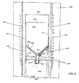
- FIG. 6 illustrates a cross-sectional view of a VGF growth system with a crucible support 2000 constructed according to an embodiment of the present invention.
- Any of the crucible-ampoule combination shown in FiGs. 1-5 or other kind of crucible-ampoule combination may rest on the crucible support 2000.
- the crucible support 2000 is depicted in a VGF furnace 1000.
- the crucible support 2000 provides physical support for and allows for thermal gradient control to the ampoule 4000 and its contents, including the raw material (not shown), seed crystal (not shown), and a crucible 3000.
- the crucible 3000 in which the raw materials melt and the crystal grows is a PBN structure with a cylindrical crystal growth zone 3010, a smaller diameter seed well cylinder 3030, and a tapered transition zone 3020.
- the crystal growth zone 3010 is open at the top of the crucible 3000 and has a diameter equal to the desired diameter of the crystal product.
- the current industry standard diameters are 4 and 6 inch wafers.
- the seed well cylinder 3030 has a closed bottom and a diameter slightly larger than that of the high quality seed crystal, e. g., about 6 - 25 mm, and a length on the order of 30 - 100 mm. Other dimensions may also be utilized.
- the major growth zone 3010 and the seed well cylinder 3030 may have straight walls or may taper outwardly on the order of one to a few degree to facilitate the removal of the crystal from the crucible 3000.
- the tapered transition zone 3020 between the growth zone 3010 and the seed well cylinder 3030 has an angled side wall pitched at approximately 45 degrees with a larger diameter equal to and connected to the growth zone wall and a narrower diameter equal to and connected to the seed well wall.
- the angled side wall may also be more steep or less steep than 45 degrees.
- the crucible 3000 Before insertion in the VGF crystal growth furnace 1000, the crucible 3000 is loaded with raw materials, capped with a crucible cap 3040, and inserted in the ampoule 4000.
- the ampoule 4000 may, for example, be made of quartz.
- the ampoule 4000 has a shape similar to that of the crucible 3000. It is cylindrical in a seed growth region 4010, cylindrical with a narrower diameter in its seed well region 4030, and has a tapered transition region 402 between the two regions.
- the crucible 3000 fits inside the ampoule 4000 with a narrow margin between them.
- the ampoule 4000 is closed at the bottom of its seed well region 403, like the crucible, and sealed on top after the crucible and raw materials are loaded.
- the bottom of the ampoule has the same funnel shape as the crucible.
- the crucible support 2000 is required to accommodate this funnel shape and hold the ampoule 4000 stable and upright inside the VGF furnace 1000.
- the ampoule-crucible combination may retain a different shape, and the basic structure of the crucible support 2000 would be changed accordingly to fit the different shape.
- stability and strength to the ampoule and its contents are provided through a solid, thin-walled cylinder 2050 of the crucible support 2000.
- the solid, thin-walled cylinder 2050 accommodates the funnel end of the ampoule structure 4000.
- the crucible support cylinder 2050 is made of a heat conducting material, preferably quartz.
- silicon carbide and ceramic may also be utilized to form the crucible support cylinder 2050.
- the cylinder 2050 makes a circle of contact with ampoule 4000, where the upper rim of the cylinder 2050 meets the shoulder of the ampoule's tapered region 4020.
- Such configuration leads to minimal solid-to-solid contact, which ensures that little or no undesirable, relatively uncontrollable heat conduction will transpire. As a result, heating is able to be generated by other, more controllable processes.
- Low density insulating material 2060 such as ceramic fiber, fills the majority of the inside of the support cylinder 2050, with only a hollow axial core 2030 in approximately the center of the insulating material 2060 left empty to receive the seed well 4030 of the ampoule 4000.
- the low-density insulating material may also comprise alumina fiber (1,800 °C), alumina-silica fiber (1,426 °C), and/or zirconia fiber (2,200 °C).
- the insulating material 2060 is carefully placed in the crucible support 2000. The weight of the ampoule 4000, as it sits on top of the cylinder 2050, pushes the insulating material 2060 down and forms the slanted insulating material edge 2020.
- the hollow core 2030 extends downward to a small distance below the bottom of the ampoule seed well 4030.
- the hollow core 2030 extends through the crucible support from the bottom of the seed well to the bottom of the furnace apparatus 1000.
- the hollow core 2030 provides a cooling path from the center of the crystal. It contributes to cooling in the seed well and in the center of the growing crystal. With this construction, heat energy can escape down through the center of the solid crystal and seed, down through this hollow core 2030 in the insulating material 2060 within the crystal support 2000.
- the temperature of the center of the cooling ingot would naturally be higher than the crystal material nearer to the outer surface. In this case, the center of the ingot in any horizontal cross section would crystallize later after its perimeter had solidified. Crystals with uniform electrical properties cannot be made under these conditions.
- heat energy is conducted down through the bottom of the ampoule 4000 and the hollow core 2030 from where it radiates back out of radiation channels 2070. It is important to reduce heat energy from the center of the growing crystal so that the isothermal layers are kept flat across the crystal diameter. Maintaining a flat crystal-melt interface allows the production of crystals with uniform electrical and physical properties.
- the low-density insulating material 2060 within the cylinder 2050 obstructs the flow of heat radiation from the furnace heat elements 1010 to the ampoule 4000 in the seed well region 4030, so this method requires the creation of a plurality of horizontal radiation channels/openings/tunnels 2070 through the insulation material 2060.
- the radiation channels 2070 penetrate the insulating material 2060 to provide heat radiation outlets to controllably transfer heat from the furnace heating elements 1010 to the ampoule seed well 4030.
- the number, shape and diameter of the radiation channels 2070 varies depending on specific conditions.
- the radiation channels may also be slanted, bent or wave-like.
- the radiation channels also do not necessary have to be continuous, as they may extend only partially through the insulating material 2060. This helps minimize convection currents.
- the diameter of these channels is small, on the order of a pencil width, so that convection airflow is insignificant. Larger holes with cross-sectional area on the order of a square inch or more can also be used according to other embodiments of the invention.
- the radiation channels 2070 through the insulating material 2060 also work in conjunction with the hollow core 2030 in the center of the insulating material 2060 to radiate heat energy drawn from the center of the crystal, and cool the crystal with planar isothermal temperature gradient layers.
- the radiation channels 2070 enable temperature control and directly relate to crystal growth yield.
- FIG. 7 illustrates a perspective view of a crucible support 2000 constructed according to the present invention.
- the exterior view of the crucible support 2000 shows a support cylinder 2050, an upper rim 2100 of the support cylinder 2050, windows 2080, insulating material 2060 and hollow core 2030.
- the support cylinder 2050 provides support to an ampoule structure (not shown) with only minimal contact to the ampoule.
- the upper rim 2100 of the support cylinder 2050 contacts the ampoule in a circle, so conduction heating is minimal.
- the cylinder also forms a barrier to airflow, blocking convection currents that might otherwise develop in the radiation channels (not shown) that leads to windows 2080, while not blocking radiated heat.
- the windows 2080 may also be the ends of the radiation channels.
- the small diameter of the radiation channels is another deterrent to convection airflow within the crucible support 2000.
- the job of conveying heat energy from the furnace heating elements to the seed well in VGF under this method is left primarily to heat radiation.
- Heat radiation is the most effective method of heat transfer in the temperature range of crystal growth furnaces, about several hundred to more than 1,200 °C, and heat radiation is the most desirable means of heating the ampoule and charge as it can be more carefully controlled than either convection or conduction.
- a support cylinder employed in this construction is transparent to heat radiation, so the support cylinder does not interfere with radiated heat transfer even while it contributes to the reduction of convection airflow as a solid barrier.
- embodiments of the present invention comprise crucible support techniques that contribute high stability to the VGF ampoule, crucible, and charge, while enabling efficient, precise temperature control of the ampoule seed well.
Landscapes
- Chemical & Material Sciences (AREA)
- Engineering & Computer Science (AREA)
- Crystallography & Structural Chemistry (AREA)
- Materials Engineering (AREA)
- Metallurgy (AREA)
- Organic Chemistry (AREA)
- Inorganic Chemistry (AREA)
- Crystals, And After-Treatments Of Crystals (AREA)
- Liquid Deposition Of Substances Of Which Semiconductor Devices Are Composed (AREA)
Applications Claiming Priority (2)
| Application Number | Priority Date | Filing Date | Title |
|---|---|---|---|
| US30318901P | 2001-07-05 | 2001-07-05 | |
| EP02749787A EP1456866B1 (de) | 2001-07-05 | 2002-07-03 | Vorrichtung zum züchten von halbleiterkristallen mit einer starren halterung mit steuerung der kohlenstoffdotierung und des spezifischen widerstands und des thermischen gradienten |
Related Parent Applications (1)
| Application Number | Title | Priority Date | Filing Date |
|---|---|---|---|
| EP02749787.4 Division | 2002-07-03 |
Publications (2)
| Publication Number | Publication Date |
|---|---|
| EP2444531A2 true EP2444531A2 (de) | 2012-04-25 |
| EP2444531A3 EP2444531A3 (de) | 2012-10-31 |
Family
ID=23170913
Family Applications (2)
| Application Number | Title | Priority Date | Filing Date |
|---|---|---|---|
| EP11186406A Withdrawn EP2444531A3 (de) | 2001-07-05 | 2002-07-03 | Verfahren und Vorrichtung zum Züchten von Halbleiterkristallen mit einem starren Träger und mit Kohlenstoffdotierung |
| EP02749787A Expired - Lifetime EP1456866B1 (de) | 2001-07-05 | 2002-07-03 | Vorrichtung zum züchten von halbleiterkristallen mit einer starren halterung mit steuerung der kohlenstoffdotierung und des spezifischen widerstands und des thermischen gradienten |
Family Applications After (1)
| Application Number | Title | Priority Date | Filing Date |
|---|---|---|---|
| EP02749787A Expired - Lifetime EP1456866B1 (de) | 2001-07-05 | 2002-07-03 | Vorrichtung zum züchten von halbleiterkristallen mit einer starren halterung mit steuerung der kohlenstoffdotierung und des spezifischen widerstands und des thermischen gradienten |
Country Status (8)
| Country | Link |
|---|---|
| US (1) | US6896729B2 (de) |
| EP (2) | EP2444531A3 (de) |
| JP (3) | JP4324467B2 (de) |
| KR (1) | KR100966182B1 (de) |
| CN (4) | CN102797032A (de) |
| AU (1) | AU2002320277A1 (de) |
| CA (1) | CA2452542C (de) |
| WO (1) | WO2003005417A2 (de) |
Cited By (1)
| Publication number | Priority date | Publication date | Assignee | Title |
|---|---|---|---|---|
| CN102828229A (zh) * | 2012-08-30 | 2012-12-19 | 天威新能源控股有限公司 | 一种铸锭用坩埚的底座 |
Families Citing this family (24)
| Publication number | Priority date | Publication date | Assignee | Title |
|---|---|---|---|---|
| US8361225B2 (en) | 2007-05-09 | 2013-01-29 | Axt, Inc. | Low etch pit density (EPD) semi-insulating III-V wafers |
| US7566641B2 (en) * | 2007-05-09 | 2009-07-28 | Axt, Inc. | Low etch pit density (EPD) semi-insulating GaAs wafers |
| JP5061728B2 (ja) * | 2007-05-30 | 2012-10-31 | 信越半導体株式会社 | シリコン単結晶の育成方法 |
| KR20090001402A (ko) * | 2007-06-29 | 2009-01-08 | 엘지전자 주식회사 | 방송 수신이 가능한 텔레매틱스 단말기 및 방송 신호 처리방법 |
| CN101555620A (zh) | 2008-04-07 | 2009-10-14 | Axt公司 | 晶体生长装置及方法 |
| KR100945668B1 (ko) * | 2008-12-11 | 2010-03-05 | (주)포티조 | Vgf법에 의한 갈륨비소 단결정 성장방법 |
| CN104109906A (zh) * | 2009-01-09 | 2014-10-22 | 住友电气工业株式会社 | 单晶制造装置、单晶的制造方法及单晶 |
| EP2501844A4 (de) * | 2009-10-08 | 2013-08-07 | Axt Inc | Kristallzüchtungsvorrichtung und -verfahren |
| JP5433632B2 (ja) * | 2011-05-25 | 2014-03-05 | Dowaエレクトロニクス株式会社 | GaAs単結晶の製造方法およびGaAs単結晶ウェハ |
| JP2013026540A (ja) * | 2011-07-25 | 2013-02-04 | Renesas Electronics Corp | 半導体集積回路装置 |
| US9206525B2 (en) | 2011-11-30 | 2015-12-08 | General Electric Company | Method for configuring a system to grow a crystal by coupling a heat transfer device comprising at least one elongate member beneath a crucible |
| CN104911690B (zh) * | 2015-07-01 | 2017-09-19 | 清远先导材料有限公司 | 一种磷化铟单晶的生长方法及生长装置 |
| CN105543953B (zh) * | 2015-12-28 | 2017-10-20 | 中国工程物理研究院化工材料研究所 | 多元化合物多晶成核控制装置及方法 |
| CN107794562B (zh) * | 2017-11-17 | 2020-05-08 | 中国工程物理研究院材料研究所 | 一种充气保护的晶体生长装置及方法 |
| CN109252220A (zh) * | 2018-12-04 | 2019-01-22 | 中国电子科技集团公司第四十六研究所 | 一种vgf/vb砷化镓单晶炉结构及生长方法 |
| CN109881253B (zh) * | 2019-01-30 | 2021-04-16 | 广东先导先进材料股份有限公司 | 半导体晶体的生长装置及方法 |
| DE102019208389A1 (de) * | 2019-06-07 | 2020-12-10 | Freiberger Compound Materials Gmbh | Verfahren zur Herstellung von Restspannungs- und versetzungsfreien AIII-BV-Substratwafern |
| CN110512275A (zh) * | 2019-09-30 | 2019-11-29 | 山西中科晶电信息材料有限公司 | 一种大尺寸晶体生长单晶炉 |
| CN111020689A (zh) * | 2019-12-13 | 2020-04-17 | 广东先导先进材料股份有限公司 | 晶体生长装置及方法 |
| CN112458535B (zh) * | 2020-11-12 | 2022-07-12 | 西北工业大学 | 一种合成锑化铝多晶材料工艺的装置及合成方法 |
| CN113136616B (zh) * | 2021-03-29 | 2022-02-08 | 大庆溢泰半导体材料有限公司 | 一种生长半绝缘砷化镓单晶的掺碳装置及掺碳方法 |
| CN114635180B (zh) * | 2022-05-19 | 2022-08-09 | 山西中科晶电信息材料有限公司 | 一种半绝缘砷化镓单晶体及其制备方法和生长装置 |
| CN117822089A (zh) * | 2023-12-04 | 2024-04-05 | 中国科学院上海硅酸盐研究所 | 一种含有异形隔板的晶体生长装置和异形隔板 |
| CN118600557B (zh) * | 2024-08-09 | 2024-12-31 | 苏州优晶半导体科技股份有限公司 | 降低发热体打火的碳化硅单晶生长装置和碳化硅单晶的生长方法 |
Family Cites Families (19)
| Publication number | Priority date | Publication date | Assignee | Title |
|---|---|---|---|---|
| JPS58500020A (ja) * | 1981-01-05 | 1983-01-06 | ウエスタ−ン エレクトリツク カムパニ−,インコ−ポレ−テツド | 半導体化合物単結晶の形成と生長を行うための方法と装置 |
| JPS6437833A (en) | 1987-08-03 | 1989-02-08 | Nippon Mining Co | Semi-insulating gaas single crystal |
| JPH01239089A (ja) * | 1987-11-30 | 1989-09-25 | Toshiba Corp | 化合物半導体単結晶の製造方法及び製造装置 |
| JPH0234597A (ja) * | 1988-07-26 | 1990-02-05 | Sumitomo Electric Ind Ltd | 水平ブリッジマン法によるGaAs単結晶の成長方法 |
| JPH0380180A (ja) * | 1989-08-23 | 1991-04-04 | Mitsubishi Monsanto Chem Co | 単結晶製造装置 |
| US4999082A (en) * | 1989-09-14 | 1991-03-12 | Akzo America Inc. | Process for producing monocrystalline group II-IV or group III-V compounds and products thereof |
| JPH04265297A (ja) * | 1990-03-30 | 1992-09-21 | Mitsubishi Materials Corp | 高解離圧化合物半導体結晶処理装置におけるシール方法、およびシール構造 |
| JPH05238870A (ja) * | 1992-02-28 | 1993-09-17 | Furukawa Electric Co Ltd:The | 化合物半導体単結晶の製造方法およびその製造装置 |
| TW230822B (de) | 1993-03-02 | 1994-09-21 | Sumitomo Electric Industries | |
| JP3391598B2 (ja) * | 1995-03-29 | 2003-03-31 | 株式会社神戸製鋼所 | 化合物半導体の単結晶製造装置及びその装置を用いた製造方法 |
| JPH09110595A (ja) * | 1995-10-16 | 1997-04-28 | Hitachi Cable Ltd | GaAs単結晶インゴットの熱処理方法 |
| JP3201305B2 (ja) * | 1996-04-26 | 2001-08-20 | 住友電気工業株式会社 | Iii−v族化合物半導体結晶の製造方法 |
| JP4120016B2 (ja) * | 1996-12-12 | 2008-07-16 | 住友電気工業株式会社 | 半絶縁性GaAs単結晶の製造方法 |
| JPH10212200A (ja) * | 1997-01-27 | 1998-08-11 | Japan Energy Corp | 半絶縁性GaAs単結晶の製造方法 |
| US6045767A (en) | 1997-11-21 | 2000-04-04 | American Xtal Technology | Charge for vertical boat growth process and use thereof |
| JP3596337B2 (ja) * | 1998-03-25 | 2004-12-02 | 住友電気工業株式会社 | 化合物半導体結晶の製造方法 |
| JPH11310499A (ja) * | 1998-04-30 | 1999-11-09 | Kobe Steel Ltd | 化合物半導体単結晶の熱処理方法およびその装置 |
| JP4067234B2 (ja) * | 1999-05-12 | 2008-03-26 | Dowaホールディングス株式会社 | アニール炉 |
| JP3656734B2 (ja) * | 2000-03-17 | 2005-06-08 | シャープ株式会社 | 液晶表示装置 |
-
2002
- 2002-07-03 JP JP2003511286A patent/JP4324467B2/ja not_active Expired - Fee Related
- 2002-07-03 US US10/190,001 patent/US6896729B2/en not_active Expired - Lifetime
- 2002-07-03 CN CN2012102571592A patent/CN102797032A/zh active Pending
- 2002-07-03 AU AU2002320277A patent/AU2002320277A1/en not_active Abandoned
- 2002-07-03 WO PCT/US2002/021195 patent/WO2003005417A2/en not_active Ceased
- 2002-07-03 KR KR1020047000105A patent/KR100966182B1/ko not_active Expired - Fee Related
- 2002-07-03 EP EP11186406A patent/EP2444531A3/de not_active Withdrawn
- 2002-07-03 CN CNA2008101475197A patent/CN101407936A/zh active Pending
- 2002-07-03 CN CNA028158652A patent/CN1543518A/zh active Pending
- 2002-07-03 CN CN2011101443037A patent/CN102220628A/zh not_active Withdrawn
- 2002-07-03 EP EP02749787A patent/EP1456866B1/de not_active Expired - Lifetime
- 2002-07-03 CA CA2452542A patent/CA2452542C/en not_active Expired - Lifetime
-
2008
- 2008-10-14 JP JP2008265616A patent/JP5005651B2/ja not_active Expired - Fee Related
-
2012
- 2012-03-30 JP JP2012078848A patent/JP2012126644A/ja active Pending
Cited By (2)
| Publication number | Priority date | Publication date | Assignee | Title |
|---|---|---|---|---|
| CN102828229A (zh) * | 2012-08-30 | 2012-12-19 | 天威新能源控股有限公司 | 一种铸锭用坩埚的底座 |
| CN102828229B (zh) * | 2012-08-30 | 2015-01-21 | 天威新能源控股有限公司 | 一种铸锭用坩埚的底座 |
Also Published As
| Publication number | Publication date |
|---|---|
| AU2002320277A1 (en) | 2003-01-21 |
| EP1456866A2 (de) | 2004-09-15 |
| CN1543518A (zh) | 2004-11-03 |
| CA2452542A1 (en) | 2003-01-16 |
| EP1456866B1 (de) | 2012-06-13 |
| US20030037721A1 (en) | 2003-02-27 |
| EP1456866A4 (de) | 2008-08-20 |
| JP2009051728A (ja) | 2009-03-12 |
| EP2444531A3 (de) | 2012-10-31 |
| CN102220628A (zh) | 2011-10-19 |
| US6896729B2 (en) | 2005-05-24 |
| KR100966182B1 (ko) | 2010-06-25 |
| JP5005651B2 (ja) | 2012-08-22 |
| WO2003005417A2 (en) | 2003-01-16 |
| KR20040018426A (ko) | 2004-03-03 |
| JP4324467B2 (ja) | 2009-09-02 |
| CN101407936A (zh) | 2009-04-15 |
| CN102797032A (zh) | 2012-11-28 |
| JP2012126644A (ja) | 2012-07-05 |
| WO2003005417A3 (en) | 2004-06-17 |
| CA2452542C (en) | 2011-04-26 |
| JP2004534710A (ja) | 2004-11-18 |
Similar Documents
| Publication | Publication Date | Title |
|---|---|---|
| CA2452542C (en) | Method and apparatus for growing semiconductor crystals with a rigid support with carbon doping and resistivity control and thermal gradient control | |
| US8231727B2 (en) | Crystal growth apparatus and method | |
| US8506706B2 (en) | Systems, methods and substrates of monocrystalline germanium crystal growth | |
| EP0140509B1 (de) | LEC-Verfahren und Vorrichtung zur Züchtung eines Einkristalls von Halbleiterverbindung | |
| EP2510138B1 (de) | Herstellungsverfahren von monokristallinen germaniumingots/-wafern mit niedriger mikrovertiefungsdichte (mpd) | |
| US20030172870A1 (en) | Apparatus for growing monocrystalline group II-VI and III-V compounds | |
| CN102272361A (zh) | 单晶锗晶体生长的系统、方法和衬底 | |
| EP2501844A1 (de) | Kristallzüchtungsvorrichtung und -verfahren | |
| WO2010053586A2 (en) | Systems, methods and substrates of monocrystalline germanium crystal growth | |
| KR102921125B1 (ko) | 실리콘 충전물을 덮기 위한 커버 부재를 갖는 결정 인상 시스템 및 도가니 조립체 내에서 실리콘의 용융물을 성장시키는 방법 | |
| JP2005132717A (ja) | 化合物半導体単結晶およびその製造方法 | |
| JP2006169031A (ja) | 化合物半導体単結晶の製造方法 | |
| JPH061692A (ja) | 化合物半導体単結晶の製造装置 | |
| JP2006327918A (ja) | GaAs単結晶の製造方法 | |
| JP2010120828A (ja) | 半導体結晶の製造方法 |
Legal Events
| Date | Code | Title | Description |
|---|---|---|---|
| AC | Divisional application: reference to earlier application |
Ref document number: 1456866 Country of ref document: EP Kind code of ref document: P |
|
| AK | Designated contracting states |
Kind code of ref document: A2 Designated state(s): DE FR GB |
|
| PUAI | Public reference made under article 153(3) epc to a published international application that has entered the european phase |
Free format text: ORIGINAL CODE: 0009012 |
|
| RIN1 | Information on inventor provided before grant (corrected) |
Inventor name: LIU, WEI GUO Inventor name: LIU, XIAO GORDON |
|
| PUAL | Search report despatched |
Free format text: ORIGINAL CODE: 0009013 |
|
| RIC1 | Information provided on ipc code assigned before grant |
Ipc: C30B 11/06 20060101AFI20120918BHEP Ipc: C30B 27/00 20060101ALI20120918BHEP Ipc: C30B 35/00 20060101ALI20120918BHEP Ipc: C30B 11/04 20060101ALI20120918BHEP Ipc: C30B 11/12 20060101ALI20120918BHEP Ipc: C30B 29/42 20060101ALI20120918BHEP |
|
| AK | Designated contracting states |
Kind code of ref document: A3 Designated state(s): DE FR GB |
|
| 17P | Request for examination filed |
Effective date: 20130429 |
|
| STAA | Information on the status of an ep patent application or granted ep patent |
Free format text: STATUS: THE APPLICATION HAS BEEN WITHDRAWN |
|
| 18W | Application withdrawn |
Effective date: 20150108 |