EP2390897B1 - Plasmaverarbeitungsvorrichtung - Google Patents
Plasmaverarbeitungsvorrichtung Download PDFInfo
- Publication number
- EP2390897B1 EP2390897B1 EP11004262.9A EP11004262A EP2390897B1 EP 2390897 B1 EP2390897 B1 EP 2390897B1 EP 11004262 A EP11004262 A EP 11004262A EP 2390897 B1 EP2390897 B1 EP 2390897B1
- Authority
- EP
- European Patent Office
- Prior art keywords
- processing
- upper electrode
- space
- processing chamber
- gas exhaust
- Prior art date
- Legal status (The legal status is an assumption and is not a legal conclusion. Google has not performed a legal analysis and makes no representation as to the accuracy of the status listed.)
- Active
Links
Images


Classifications
-
- H—ELECTRICITY
- H01—ELECTRIC ELEMENTS
- H01J—ELECTRIC DISCHARGE TUBES OR DISCHARGE LAMPS
- H01J37/00—Discharge tubes with provision for introducing objects or material to be exposed to the discharge, e.g. for the purpose of examination or processing thereof
- H01J37/32—Gas-filled discharge tubes
- H01J37/32431—Constructional details of the reactor
- H01J37/32623—Mechanical discharge control means
- H01J37/32633—Baffles
-
- C—CHEMISTRY; METALLURGY
- C23—COATING METALLIC MATERIAL; COATING MATERIAL WITH METALLIC MATERIAL; CHEMICAL SURFACE TREATMENT; DIFFUSION TREATMENT OF METALLIC MATERIAL; COATING BY VACUUM EVAPORATION, BY SPUTTERING, BY ION IMPLANTATION OR BY CHEMICAL VAPOUR DEPOSITION, IN GENERAL; INHIBITING CORROSION OF METALLIC MATERIAL OR INCRUSTATION IN GENERAL
- C23C—COATING METALLIC MATERIAL; COATING MATERIAL WITH METALLIC MATERIAL; SURFACE TREATMENT OF METALLIC MATERIAL BY DIFFUSION INTO THE SURFACE, BY CHEMICAL CONVERSION OR SUBSTITUTION; COATING BY VACUUM EVAPORATION, BY SPUTTERING, BY ION IMPLANTATION OR BY CHEMICAL VAPOUR DEPOSITION, IN GENERAL
- C23C16/00—Chemical coating by decomposition of gaseous compounds, without leaving reaction products of surface material in the coating, i.e. chemical vapour deposition [CVD] processes
- C23C16/44—Chemical coating by decomposition of gaseous compounds, without leaving reaction products of surface material in the coating, i.e. chemical vapour deposition [CVD] processes characterised by the method of coating
- C23C16/455—Chemical coating by decomposition of gaseous compounds, without leaving reaction products of surface material in the coating, i.e. chemical vapour deposition [CVD] processes characterised by the method of coating characterised by the method used for introducing gases into reaction chamber or for modifying gas flows in reaction chamber
- C23C16/45563—Gas nozzles
- C23C16/45565—Shower nozzles
-
- H—ELECTRICITY
- H01—ELECTRIC ELEMENTS
- H01J—ELECTRIC DISCHARGE TUBES OR DISCHARGE LAMPS
- H01J37/00—Discharge tubes with provision for introducing objects or material to be exposed to the discharge, e.g. for the purpose of examination or processing thereof
- H01J37/32—Gas-filled discharge tubes
- H01J37/32431—Constructional details of the reactor
- H01J37/3244—Gas supply means
- H01J37/32449—Gas control, e.g. control of the gas flow
-
- H—ELECTRICITY
- H01—ELECTRIC ELEMENTS
- H01J—ELECTRIC DISCHARGE TUBES OR DISCHARGE LAMPS
- H01J37/00—Discharge tubes with provision for introducing objects or material to be exposed to the discharge, e.g. for the purpose of examination or processing thereof
- H01J37/32—Gas-filled discharge tubes
- H01J37/32431—Constructional details of the reactor
- H01J37/32458—Vessel
- H01J37/32477—Vessel characterised by the means for protecting vessels or internal parts, e.g. coatings
-
- H—ELECTRICITY
- H01—ELECTRIC ELEMENTS
- H01J—ELECTRIC DISCHARGE TUBES OR DISCHARGE LAMPS
- H01J37/00—Discharge tubes with provision for introducing objects or material to be exposed to the discharge, e.g. for the purpose of examination or processing thereof
- H01J37/32—Gas-filled discharge tubes
- H01J37/32431—Constructional details of the reactor
- H01J37/32532—Electrodes
- H01J37/32568—Relative arrangement or disposition of electrodes; moving means
-
- H—ELECTRICITY
- H01—ELECTRIC ELEMENTS
- H01J—ELECTRIC DISCHARGE TUBES OR DISCHARGE LAMPS
- H01J37/00—Discharge tubes with provision for introducing objects or material to be exposed to the discharge, e.g. for the purpose of examination or processing thereof
- H01J37/32—Gas-filled discharge tubes
- H01J37/32431—Constructional details of the reactor
- H01J37/32623—Mechanical discharge control means
- H01J37/32651—Shields, e.g. dark space shields, Faraday shields
-
- H—ELECTRICITY
- H01—ELECTRIC ELEMENTS
- H01J—ELECTRIC DISCHARGE TUBES OR DISCHARGE LAMPS
- H01J37/00—Discharge tubes with provision for introducing objects or material to be exposed to the discharge, e.g. for the purpose of examination or processing thereof
- H01J37/32—Gas-filled discharge tubes
- H01J37/32431—Constructional details of the reactor
- H01J37/32798—Further details of plasma apparatus not provided for in groups H01J37/3244 - H01J37/32788; special provisions for cleaning or maintenance of the apparatus
- H01J37/32816—Pressure
- H01J37/32834—Exhausting
Definitions
- the present disclosure relates to a plasma processing apparatus including an upper electrode capable of vertically moving within a processing chamber.
- a plasma processing apparatus for manufacturing a semiconductor device there is widely used a so-called parallel plate type plasma processing apparatus which includes a lower electrode for mounting thereon a substrate such as a semiconductor wafer, a liquid crystal substrate or the like; and an upper electrode disposed to face the lower electrode in a processing chamber.
- the substrate is mounted on the lower electrode, a processing gas is introduced toward the lower electrode through a multiple number of discharge holes formed in the upper electrode, and then plasma of the processing gas is generated by applying a high frequency power between the electrodes. Accordingly, a plasma process such as an etching process or a film formation process is performed on the substrate.
- a distance between the upper electrode and the lower electrode may affect plasma processing characteristics on the substrate. Therefore, the distance needs to be accurately adjusted depending on processing conditions or types of plasma processes. Especially, when different types of plasma processes or plasma processes having different processing conditions are continuously performed in the same processing chamber, the distance needs to be adjusted to an optimal distance for each of the plasma processes. For this reason, conventionally, there has been developed a plasma processing apparatus capable of optimally adjusting a distance between an upper electrode and a lower electrode by vertically moving the upper electrode (see, e.g., Patent Document 1).
- the plasma processing apparatus described in Patent Document 1 is configured to vertically move the upper electrode between a ceiling wall of a processing chamber and the lower electrode by installing the upper electrode at the ceiling wall of the processing chamber via a bellows. With this configuration, the distance between the upper electrode and the lower electrode (distance between electrodes) can be adjusted by vertically moving the upper electrode.
- Patent Document 1 Japanese Patent Laid-open Publication No. 2005-93843
- the processing gas introduced in this space may be hardly exhausted even by driving a vacuum pump.
- the processing gas remaining in this space may flow downward toward a processing space below the upper electrode. This may affect plasma processing characteristics.
- a pressure may be increased. Hence, abnormal electric discharge may occur in the space when a high frequency power is applied between the electrodes.
- Document JP H03 145124 A discloses a plasma processing apparatus for performing a plasma process on a substrate comprising a lower electrode, an upper electrode, a power supply unit, a shield sidewall surrounding the electrodes and a processing space between the electrode, an inner gas exhaust path formed at the inside of the shield sidewall and configured to exhaust an atmosphere in the processing space, and an outer gas exhaust path formed at the outside of the shield sidewall and configured to exhaust the processing gas introduced into a space between the upper electrode and a ceiling wall of the processing chamber.
- Further plasma processing apparatuses are disclosed in documents JP H10 302998 A , JP H08 199364 A and US 2007/221130 A1 .
- the present disclosure provides a plasma processing apparatus capable of easily exhausting a processing gas introduced in a space above a vertically movable upper electrode, thereby preventing abnormal electrical discharge from occurring in the space above the upper electrode.
- a plasma processing apparatus for performing a plasma process on a substrate in a processing chamber.
- the plasma processing apparatus includes a lower electrode installed at a bottom wall of the processing chamber and configured to mount thereon the substrate; an upper electrode installed so as to face the lower electrode and having a plurality of discharge holes for introducing a processing gas toward the substrate; a power supply unit configured to supply a high frequency power for generating plasma of the processing gas between the electrodes; an elevation unit installed at a ceiling wall of the processing chamber and configured to elevate the upper electrode between the ceiling wall and the lower electrode; a cylindrical wall configured to surround the electrodes and a processing space between the electrodes; an inner gas exhaust path formed at the inside of the cylindrical wall and configured to exhaust an atmosphere in the processing space; and an outer gas exhaust path formed at the outside of the cylindrical wall and configured to exhaust the processing gas introduced into a space between the upper electrode and the ceiling wall.
- the processing gas supplied into the processing space inside the cylindrical wall is introduced in the space (space above the upper electrode) between the ceiling wall and the upper electrode from the gap between the upper electrode and the cylindrical wall, the processing can be easily exhausted through a gas exhaust port via the outer gas exhaust path. Further, a pressure in the space above the upper electrode can be maintained at a low level, so that abnormal electrical discharge can be prevented from occurring in the space.
- the cylindrical wall is a shield sidewall provided at the inside of a sidewall of the processing chamber
- the outer gas exhaust path may include a gas exhaust space formed between the sidewall of the processing chamber and the shield sidewall.
- a flange protruded so as to block the outer gas exhaust path is secured to an upper portion of the shield sidewall, and the flange is provided with a plurality of communicating holes that allows the outer gas exhaust path to communicate with the space between the upper electrode and the ceiling wall.
- a conductance of the outer gas exhaust path may be adjusted by changing the number or the shape of the communication holes.
- a groove is formed in the flange along a periphery of the shield sidewall, and the communication holes are formed in a bottom of the groove. Moreover, a plurality of communication holes is formed in the shield sidewall so as to allow a space in the groove to communicate with a gap between the upper electrode and the shield sidewall.
- the cylindrical wall may be the sidewall of the processing chamber
- the outer gas exhaust path may be a bypass line that allows the space between the upper electrode and the ceiling wall to communicate with a gas exhaust line connected to a gas exhaust port of the processing chamber. Accordingly, the present disclosure is applicable to a plasma processing apparatus in which the shield sidewall is not installed.
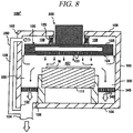
- a lower electrode (susceptor) 111 serving as a part of a mounting table 110 for mounting thereon a wafer W and an upper electrode 120 installed so as to face the lower electrode 111 and serving as a shower head for introducing a processing gas, a purge gas or the like.
- the lower electrode 111 is made of, e.g., aluminum and is installed at the bottom wall 104 of the processing chamber 102 via a cylindrical insulating support 106. Further, the lower electrode 111 is formed in a columnar shape so as to correspond to an outer diameter of the wafer W.
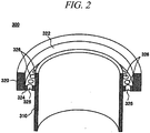
- the upper electrode 120 is supported at the ceiling wall 105 of the processing chamber 102 so as to be elevatable by an upper electrode elevation unit 200. Accordingly, a distance between the lower electrode 111 and the upper electrode 120 can be adjusted.
- the upper electrode elevation unit 200 will be described in detail later.
- the upper electrode 120 may include an electrode plate 124 serving as a facing surface to the lower electrode 111 and having a multiple number of discharge holes 123; and an electrode support 125 for supporting the electrode plate 124.
- the electrode plate 124 is made of, e.g., quartz and the electrode support 125 is made of, e.g., a conductive material such as aluminum whose surface is alumite treated.
- the upper electrode elevation unit 200 of Fig. 1 may include a substantially cylindrical sliding support member 204 for supporting and slidably moving the upper electrode 120 within the processing chamber 102.
- the sliding support member 204 is installed substantially at a center of the upper portion of the upper electrode 120 by bolts or the like.
- the slide unit 210 may include a guide member 216 fixed to a vertical portion of a fixing member 214 installed at an upper portion of the processing chamber 102 and having an L-shaped cross section; and a rail member 212 slidably supported by the guide member 216 and formed in one direction (vertical direction in the present embodiment) on the outer peripheral surface of the sliding support member 204.
- a horizontal portion of the fixing member 214 for fixing the guide member 216 of the slide unit 210 is fixed to the upper portion of the processing chamber 102 via an annular horizontality adjustment plate 218.
- the horizontality adjustment plate 218 is configured to adjust a horizontal position of the upper electrode 120.
- the horizontality adjustment plate 218 may be fixed to the processing chamber 102 by a multiple number of bolts spaced apart from each other at a regular interval along a periphery of the horizontality adjustment plate 218, and an inclination of the horizontality adjustment plate 218 with respect to a horizontal plane can be varied by adjusting a protruding degree of the bolts.
- the air pressure cylinder 220 has a rod 202 capable of moving in one direction, and a lower end of the rod 202 is connected to a substantially upper central portion of the sliding support member 204 by bolts or the like. With this configuration, by moving the rod 202 of the air pressure cylinder 220, the upper electrode 120 is moved in one direction along the slide unit by the sliding support member 204.
- the rod 202 is formed in a cylindrical shape, and an inner space of the rod 202 communicates with a central hole formed substantially at a center of the sliding support member 204 and opens to the atmosphere. Accordingly, wiring such as a grounding wire (not shown in Fig. 1 ) can be connected to the upper electrode 120 through the inner space of the rod 202 and the central hole of the sliding support member 204.
- the second high frequency power supply unit 152 may include a second filter 154, a second matching unit 156 and a second power supply 158 connected in sequence from the lower electrode 111.
- the second filter 154 prevents a power component of the first frequency from entering the second matching unit 156.
- the second matching unit 156 matches a component of the second high frequency power.
- a controller (overall control unit) 160 is connected to the plasma processing apparatus 100. Each part of the plasma processing apparatus 100 is controlled by the controller 160. Further, the controller 160 is connected to a manipulation unit 162 including a keyboard through which an operator inputs commands to manage the plasma processing apparatus 100 or a display which visually displays an operation status of the plasma processing apparatus 100.
- controller 160 is connected to a storage unit 164 that stores therein: programs for implementing various processes (e.g., etching, ashing, or film formation) performed in the plasma processing apparatus 100 under the control of the controller 160; and processing conditions (recipes) required for executing the programs.
- programs for implementing various processes e.g., etching, ashing, or film formation
- processing conditions e.g., etching, ashing, or film formation
- the controller 160 reads out a program and processing condition from the storage unit 164 in response to an instruction from the manipulation unit 162 and controls each part, thereby carrying out a desired process in the plasma processing apparatus 100. Further, the processing condition can be edited by the manipulation unit 162.
- a distance between electrodes is adjusted by vertically moving the upper electrode 120. Further, the processing gas is introduced toward a processing space 107 above the lower electrode via the upper electrode 120 from the processing gas supply unit 130, and the first and the second high frequency powers are applied to the lower electrode 111. Accordingly, plasma of the processing gas is generated and a plasma process such as etching or film formation is performed on the wafer W mounted on the mounting table 110.
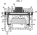
- a cylindrical wall surrounding the electrodes 111 and 120 and the processing space 107 is formed, and an outer gas exhaust path 138 for directly exhausting the processing gas introduced into the space 108 between the upper electrode 120 and the ceiling wall 105 is formed at the outside of the cylindrical wall.
- Fig. 1 shows a shield sidewall 310 of a shield member 300 serving as the cylindrical wall surrounding the electrodes 111 and 120 and the processing space 107.
- the outer gas exhaust path 138 is formed between the shield sidewall 310 and the sidewall 103 of the processing chamber 102 and serves as a gas exhaust space communicating with the gas exhaust port 132.
- the shield member 300 may be configured as shown in Fig. 2 , for example.
- the shield member 300 may include the shield sidewall 310 and a flange 320 attached to an upper portion of the shield sidewall 310.
- the shield sidewall 310 and the flange 320 may be formed as a single part or as separate parts.
- a groove 322 is formed at the flange 320 along the circumference of the shield sidewall 310.
- a multiple number of communication holes 326 are formed so as to allow the space 108 above the upper electrode 120 to communicate with the outer gas exhaust path 138.
- a conductance of the outer gas exhaust path 138 can be adjusted by changing the number or the shape of the communication holes 326.
- the conductance of the outer gas exhaust path 138 may be set to be greater than a conductance of a gap between the upper electrode 120 and the shield sidewall 310.
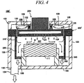
- the outer gas exhaust path 138 is not provided as shown in Fig. 4 , it may be extremely difficult to exhaust the processing gas that has been introduced into the space 108 above the upper electrode 120, and the processing gas is highly likely to remain in the space 108.
- the outer gas exhaust path 138 is provided as shown in Fig. 3 , the processing gas that has been introduced into the space 108 above the upper electrode 120 can be easily exhausted directly from the gas exhaust port 132 through the outer gas exhaust path 138. As a consequence, it is possible to prevent the processing gas from remaining in the space 108 above the upper electrode 120.
- a pressure in the space 108 above the upper electrode 120 can be maintained at a low level, so that abnormal electrical discharge can be prevented from occurring in the space 108.
- the conductance of the outer gas exhaust path 138 can be set to be greater than the conductance of the gap (gap into which the processing gas is introduced) formed around the upper electrode 120. Accordingly, the processing gas that has been introduced into the space 108 above the upper electrode 120 can be more easily exhausted from the gas exhaust port 132.
- the configuration of the shield member 300 is not limited to the example shown in Fig. 2 .
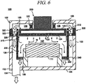
- communication holes 312 may be formed at the shield sidewall 310 so as to allow a space of the groove 322 of the flange 320 to communicate with the gap between the upper electrode 120 and the shield sidewall 310.
- the processing gas introduced into the gap formed around the upper electrode 120 can also be flown to the outer gas exhaust path 138 through the communication holes 312 and 326, as can be seen from Fig. 6 . Accordingly, the processing gas inside the shield sidewall 310 can be prevented from entering the space 108 above the upper electrode 120.
- the bypass line 350 serving as the outer exhaust path 138 in a plasma processing apparatus 100" in which the shield sidewall 310 is not installed.
- the sidewall 103 of the processing chamber 102 may serve as a cylindrical wall surrounding the electrodes 120 and 111 and the processing space 107. With this configuration, it is possible to prevent the processing gas from remaining in the space 108 above the upper electrode 120.
Landscapes
- Chemical & Material Sciences (AREA)
- Engineering & Computer Science (AREA)
- Physics & Mathematics (AREA)
- Plasma & Fusion (AREA)
- Analytical Chemistry (AREA)
- Power Engineering (AREA)
- General Chemical & Material Sciences (AREA)
- Chemical Kinetics & Catalysis (AREA)
- Materials Engineering (AREA)
- Mechanical Engineering (AREA)
- Metallurgy (AREA)
- Organic Chemistry (AREA)
- Drying Of Semiconductors (AREA)
- Plasma Technology (AREA)
- Chemical Vapour Deposition (AREA)
Claims (3)
- Plasmaprozessvorrichtung (100) zum Ausführen eines Plasmaprozesses an einem Substrat (W) in einer Prozesskammer (102), wobei die Vorrichtung (100) umfasst:die Prozesskammer (102);eine untere Elektrode (111), die an einer Bodenwand (104) der Prozesskammer (102) installiert und derart konfiguriert ist, daran das Substrat (W) zu montieren;eine obere Elektrode (120), die so installiert ist, dass sie der unteren Elektrode (111) zugewandt ist und eine Mehrzahl von Austragslöchern (123) zum Einführen eines Prozessgases im Gebrauch in Richtung des Substrats (W) aufweist;eine Energieversorgungseinheit (140), die derart konfiguriert ist, eine Hochfrequenzleistung zu liefern, so dass im Gebrauch ein Plasma des Prozessgases zwischen den Elektroden (111, 120) erzeugt wird;eine Abschirmseitenwand (310), die an der Innenseite der Seitenwand der Prozesskammer (102) vorgesehen und derart konfiguriert ist, die Elektroden (111, 120) sowie einen Prozessraum (107) zwischen den Elektroden (111, 120) zu umgeben;einen inneren Abgaspfad (330), der an der Innenseite der Abschirmseitenwand (310) geformt und derart konfiguriert ist, im Gebrauch eine Atmosphäre in dem Prozessraum (107) auszutragen; undeinen äußeren Abgaspfad (138), der an der Außenseite der Abschirmseitenwand (310) gebildet ist, derart konfiguriert ist, im Gebrauch das Prozessgas auszutragen, das in einen Raum zwischen der oberen Elektrode (120) und einer Deckenwand (105) der Prozesskammer (102) eingeführt wird, und einen Abgasraum aufweist, der zwischen der Seitenwand der Prozesskammer (102) und der Abschirmseitenwand (310) gebildet ist, gekennzeichnet durcheine Anhebeinheit (200), die an der Deckenwand (105) der Prozesskammer (102) montiert und derart konfiguriert ist, die obere Elektrode (120) zwischen der Deckenwand (105) und der unteren Elektrode (111) anzuheben,wobei ein Flansch (320), der so vorragt, dass er den äußeren Abgaspfad (138) blockiert, an einem oberen Abschnitt der Abschirmseitenwand (310) angebracht ist, wobei eine Nut (322) in dem Flansch (320) entlang eines Umfangs der Abschirmseitenwand (310) gebildet ist, wobei eine Mehrzahl erster Kommunikationslöcher (326) in einem Boden der Nut (322) gebildet ist, um so eine Kommunikation des äußeren Abgaspfades (138) mit dem Raum zwischen der oberen Elektrode (120) und der Deckenwand (105) zu ermöglichen, undwobei eine Mehrzahl zweiter Kommunikationslöcher (312) in der Abschirmseitenwand (310) geformt ist, um so eine Kommunikation eines Raumes in der Nut (322) mit einem Spalt zwischen der oberen Elektrode (120) und der Abschirmseitenwand (310) zu ermöglichen.
- Plasmaprozessvorrichtung (100) zum Ausführen eines Plasmaprozesses an einem Substrat (W) in einer Prozesskammer (102), wobei die Vorrichtung (100) umfasst:die Prozesskammer (102);eine untere Elektrode (111), die an einer Bodenwand (104) der Prozesskammer (102) installiert und derart konfiguriert ist, daran das Substrat (W) zu montieren;eine obere Elektrode (120), die so installiert ist, dass sie zu der unteren Elektrode (111) weist und eine Mehrzahl von Austragslöchern (123) zum Einführen eines Prozessgases im Gebrauch in Richtung des Substrats (W) aufweist;eine Energieversorgungseinheit (140), die derart konfiguriert ist, eine Hochfrequenzleistung so zu liefern, dass im Gebrauch ein Plasma des Prozessgases zwischen den Elektroden (111, 120) erzeugt wird;eine Abschirmseitenwand (310), die an der Innenseite der Seitenwand der Prozesskammer (102) vorgesehen und derart konfiguriert ist, die Elektroden (111, 120) und einen Prozessraum (107) zwischen den Elektroden (111, 120) zu umgeben;einen inneren Abgaspfad (330), der an der Innenseite der Abschirmseitenwand (310) gebildet und derart konfiguriert ist, im Gebrauch eine Atmosphäre in dem Prozessraum (107) auszutragen; undeinen äußeren Abgaspfad (138), der an der Außenseite der Abschirmseitenwand (310) gebildet ist, derart konfiguriert ist, im Gebrauch das Prozessgas auszutragen, das in einen Raum zwischen der oberen Elektrode (120) und einer Deckenwand (105) der Prozesskammer (102) eingeführt ist, und einen Abgasraum aufweist, der zwischen der Seitenwand der Prozesskammer (102) und der Abschirmseitenwand (310) gebildet ist, gekennzeichnet durcheine Anhebeinheit (200), die an der Deckenwand (105) der Prozesskammer (102) installiert und derart konfiguriert ist, die obere Elektrode (120) zwischen der Deckenwand (105) und der unteren Elektrode (111) anzuheben,wobei ein Flansch (320), der so vorragt, um den äußeren Abgaspfad (138) zu blockieren, an einem oberen Abschnitt der Abschirmseitenwand (310) befestigt ist,der Flansch (320) mit einer Mehrzahl von Kommunikationslöchern (326) versehen ist, die so angeordnet sind, dass sie eine Kommunikation des äußeren Abgaspfades (138) mit dem Raum zwischen der oberen Elektrode (120) und der Deckenwand (105) ermöglichen, undwobei die Kommunikationslöcher (326) so angeordnet sind, dass ihre Anzahl oder ihre Form so geändert werden kann, um eine Leitfähigkeit des äußeren Abgaspfades (138) einzustellen.
- Plasmaprozessvorrichtung (100) zum Ausführen eines Plasmaprozesses an einem Substrat (W) in einer Prozesskammer (102), wobei die Vorrichtung (100) umfasst:die Prozesskammer (102);eine untere Elektrode (111), die an einer Bodenwand (104) der Prozesskammer (102) installiert und derart konfiguriert ist, daran das Substrat (W) zu montieren;eine obere Elektrode (120), die so installiert ist, dass sie der unteren Elektrode (111) zugewandt ist und eine Mehrzahl von Austragslöchern (123) zum Einführen eines Prozessgases im Gebrauch in Richtung des Substrats (W) aufweist;eine Energieversorgungseinheit (140), die derart konfiguriert ist, eine Hochfrequenzleistung so zu liefern, dass im Gebrauch ein Plasma des Prozessgases zwischen den Elektroden (111, 120) erzeugt wird;eine zylindrische Wand (310), die derart konfiguriert ist, die Elektroden (111, 120) sowie einen Prozessraum (107) zwischen den Elektroden (111, 120) zu umgeben;einen inneren Abgaspfad (330), der an der Innenseite der zylindrischen Wand (310) geformt und derart konfiguriert ist, im Gebrauch eine Atmosphäre in dem Prozessraum (107) auszutragen; undeinen äußeren Abgaspfad (138), der an der Außenseite der zylindrischen Wand (310) geformt und derart konfiguriert ist, im Gebrauch das Prozessgas auszutragen, das in einen Raum zwischen der oberen Elektrode (120) und einer Deckenwand (105) der Prozesskammer (102) eingeführt ist,gekennzeichnet durcheine Anhebeinheit (200), die an der Deckenwand (105) der Prozesskammer (102) installiert und derart konfiguriert ist, die obere Elektrode (120) zwischen der Deckenwand (105) und der unteren Elektrode (111) anzuheben,wobei die zylindrische Wand (310) die Seitenwand der Prozesskammer (102) ist, undder äußere Abgaspfad (138) eine Bypassleitung ist, die so angeordnet ist, um eine Kommunikation des Raumes zwischen der oberen Elektrode (120) und der Deckenwand (105) mit einer Abgasleitung (134) zu ermöglichen, die mit einem Abgasdurchlass (132) der Prozesskammer (102) verbunden ist.
Applications Claiming Priority (1)
| Application Number | Priority Date | Filing Date | Title |
|---|---|---|---|
| JP2010119547A JP5567392B2 (ja) | 2010-05-25 | 2010-05-25 | プラズマ処理装置 |
Publications (3)
| Publication Number | Publication Date |
|---|---|
| EP2390897A2 EP2390897A2 (de) | 2011-11-30 |
| EP2390897A3 EP2390897A3 (de) | 2014-04-30 |
| EP2390897B1 true EP2390897B1 (de) | 2019-08-21 |
Family
ID=44117156
Family Applications (1)
| Application Number | Title | Priority Date | Filing Date |
|---|---|---|---|
| EP11004262.9A Active EP2390897B1 (de) | 2010-05-25 | 2011-05-24 | Plasmaverarbeitungsvorrichtung |
Country Status (6)
| Country | Link |
|---|---|
| US (1) | US8858754B2 (de) |
| EP (1) | EP2390897B1 (de) |
| JP (1) | JP5567392B2 (de) |
| KR (1) | KR101737014B1 (de) |
| CN (1) | CN102262999B (de) |
| TW (1) | TWI522014B (de) |
Families Citing this family (77)
| Publication number | Priority date | Publication date | Assignee | Title |
|---|---|---|---|---|
| JP5445252B2 (ja) * | 2010-03-16 | 2014-03-19 | 東京エレクトロン株式会社 | 成膜装置 |
| JP5567392B2 (ja) * | 2010-05-25 | 2014-08-06 | 東京エレクトロン株式会社 | プラズマ処理装置 |
| US8906160B2 (en) * | 2010-12-23 | 2014-12-09 | Intermolecular, Inc. | Vapor based processing system with purge mode |
| JP5902896B2 (ja) * | 2011-07-08 | 2016-04-13 | 東京エレクトロン株式会社 | 基板処理装置 |
| TWI661746B (zh) | 2011-10-05 | 2019-06-01 | 應用材料股份有限公司 | 電漿處理設備及其蓋組件(一) |
| US9896769B2 (en) | 2012-07-20 | 2018-02-20 | Applied Materials, Inc. | Inductively coupled plasma source with multiple dielectric windows and window-supporting structure |
| US10170279B2 (en) | 2012-07-20 | 2019-01-01 | Applied Materials, Inc. | Multiple coil inductively coupled plasma source with offset frequencies and double-walled shielding |
| US9928987B2 (en) | 2012-07-20 | 2018-03-27 | Applied Materials, Inc. | Inductively coupled plasma source with symmetrical RF feed |
| US9082590B2 (en) | 2012-07-20 | 2015-07-14 | Applied Materials, Inc. | Symmetrical inductively coupled plasma source with side RF feeds and RF distribution plates |
| US10249470B2 (en) | 2012-07-20 | 2019-04-02 | Applied Materials, Inc. | Symmetrical inductively coupled plasma source with coaxial RF feed and coaxial shielding |
| US9449794B2 (en) | 2012-07-20 | 2016-09-20 | Applied Materials, Inc. | Symmetrical inductively coupled plasma source with side RF feeds and spiral coil antenna |
| US9132436B2 (en) | 2012-09-21 | 2015-09-15 | Applied Materials, Inc. | Chemical control features in wafer process equipment |
| JP2014082354A (ja) * | 2012-10-17 | 2014-05-08 | Hitachi High-Technologies Corp | プラズマ処理装置 |
| US10256079B2 (en) | 2013-02-08 | 2019-04-09 | Applied Materials, Inc. | Semiconductor processing systems having multiple plasma configurations |
| CN107221487B (zh) | 2013-03-15 | 2019-06-28 | 应用材料公司 | 具有高度对称四重式气体注入的等离子体反应器 |
| JP2015090916A (ja) * | 2013-11-06 | 2015-05-11 | 東京エレクトロン株式会社 | 基板処理装置及び基板処理方法 |
| CN103646841B (zh) * | 2013-11-22 | 2016-01-27 | 上海华力微电子有限公司 | 一种等离子体刻蚀设备 |
| KR101560623B1 (ko) * | 2014-01-03 | 2015-10-15 | 주식회사 유진테크 | 기판처리장치 및 기판처리방법 |
| US9852905B2 (en) * | 2014-01-16 | 2017-12-26 | Taiwan Semiconductor Manufacturing Company, Ltd. | Systems and methods for uniform gas flow in a deposition chamber |
| JP2015142016A (ja) * | 2014-01-29 | 2015-08-03 | 東京エレクトロン株式会社 | 基板処理装置 |
| JP6438320B2 (ja) * | 2014-06-19 | 2018-12-12 | 東京エレクトロン株式会社 | プラズマ処理装置 |
| US11637002B2 (en) | 2014-11-26 | 2023-04-25 | Applied Materials, Inc. | Methods and systems to enhance process uniformity |
| JP6423706B2 (ja) * | 2014-12-16 | 2018-11-14 | 東京エレクトロン株式会社 | プラズマ処理装置 |
| US20160225652A1 (en) | 2015-02-03 | 2016-08-04 | Applied Materials, Inc. | Low temperature chuck for plasma processing systems |
| US10167552B2 (en) * | 2015-02-05 | 2019-01-01 | Lam Research Ag | Spin chuck with rotating gas showerhead |
| US9741593B2 (en) | 2015-08-06 | 2017-08-22 | Applied Materials, Inc. | Thermal management systems and methods for wafer processing systems |
| US10504700B2 (en) | 2015-08-27 | 2019-12-10 | Applied Materials, Inc. | Plasma etching systems and methods with secondary plasma injection |
| US10157755B2 (en) * | 2015-10-01 | 2018-12-18 | Lam Research Corporation | Purge and pumping structures arranged beneath substrate plane to reduce defects |
| US10763082B2 (en) * | 2016-03-04 | 2020-09-01 | Taiwan Semiconductor Manufacturing Co., Ltd. | Chamber of plasma system, liner for plasma system and method for installing liner to plasma system |
| US10600621B2 (en) * | 2016-03-30 | 2020-03-24 | Tokyo Electron Limited | Plasma electrode and plasma processing device |
| JP6394641B2 (ja) * | 2016-04-25 | 2018-09-26 | トヨタ自動車株式会社 | プラズマ装置 |
| US10504754B2 (en) | 2016-05-19 | 2019-12-10 | Applied Materials, Inc. | Systems and methods for improved semiconductor etching and component protection |
| KR102553629B1 (ko) * | 2016-06-17 | 2023-07-11 | 삼성전자주식회사 | 플라즈마 처리 장치 |
| US9865484B1 (en) | 2016-06-29 | 2018-01-09 | Applied Materials, Inc. | Selective etch using material modification and RF pulsing |
| US10546729B2 (en) | 2016-10-04 | 2020-01-28 | Applied Materials, Inc. | Dual-channel showerhead with improved profile |
| CN106373868B (zh) * | 2016-10-10 | 2020-03-10 | 昆山龙腾光电股份有限公司 | 一种阵列基板的制造方法 |
| US10559451B2 (en) * | 2017-02-15 | 2020-02-11 | Applied Materials, Inc. | Apparatus with concentric pumping for multiple pressure regimes |
| USD838681S1 (en) * | 2017-04-28 | 2019-01-22 | Applied Materials, Inc. | Plasma chamber liner |
| USD842259S1 (en) * | 2017-04-28 | 2019-03-05 | Applied Materials, Inc. | Plasma chamber liner |
| USD837754S1 (en) * | 2017-04-28 | 2019-01-08 | Applied Materials, Inc. | Plasma chamber liner |
| JP7176860B6 (ja) | 2017-05-17 | 2022-12-16 | アプライド マテリアルズ インコーポレイテッド | 前駆体の流れを改善する半導体処理チャンバ |
| US11276590B2 (en) | 2017-05-17 | 2022-03-15 | Applied Materials, Inc. | Multi-zone semiconductor substrate supports |
| US11276559B2 (en) | 2017-05-17 | 2022-03-15 | Applied Materials, Inc. | Semiconductor processing chamber for multiple precursor flow |
| US10297458B2 (en) | 2017-08-07 | 2019-05-21 | Applied Materials, Inc. | Process window widening using coated parts in plasma etch processes |
| JP6896565B2 (ja) * | 2017-08-25 | 2021-06-30 | 東京エレクトロン株式会社 | インナーウォール及び基板処理装置 |
| US11670490B2 (en) | 2017-09-29 | 2023-06-06 | Taiwan Semiconductor Manufacturing Co., Ltd. | Integrated circuit fabrication system with adjustable gas injector |
| US11328909B2 (en) | 2017-12-22 | 2022-05-10 | Applied Materials, Inc. | Chamber conditioning and removal processes |
| WO2019146456A1 (ja) * | 2018-01-26 | 2019-08-01 | 東京エレクトロン株式会社 | 基板処理装置 |
| US10964512B2 (en) | 2018-02-15 | 2021-03-30 | Applied Materials, Inc. | Semiconductor processing chamber multistage mixing apparatus and methods |
| US10319600B1 (en) | 2018-03-12 | 2019-06-11 | Applied Materials, Inc. | Thermal silicon etch |
| CN108588818A (zh) * | 2018-04-17 | 2018-09-28 | 陕西飞米企业管理合伙企业(有限合伙) | 一种用于气相沉积设备反应室内的尾气收集环 |
| US10699879B2 (en) | 2018-04-17 | 2020-06-30 | Applied Materials, Inc. | Two piece electrode assembly with gap for plasma control |
| KR102516885B1 (ko) * | 2018-05-10 | 2023-03-30 | 삼성전자주식회사 | 증착 장비 및 이를 이용한 반도체 장치 제조 방법 |
| CN108987235B (zh) * | 2018-07-12 | 2020-06-05 | 昆山龙腾光电股份有限公司 | 一种等离子体处理装置 |
| US11049755B2 (en) | 2018-09-14 | 2021-06-29 | Applied Materials, Inc. | Semiconductor substrate supports with embedded RF shield |
| US11062887B2 (en) | 2018-09-17 | 2021-07-13 | Applied Materials, Inc. | High temperature RF heater pedestals |
| US11417534B2 (en) | 2018-09-21 | 2022-08-16 | Applied Materials, Inc. | Selective material removal |
| US11682560B2 (en) | 2018-10-11 | 2023-06-20 | Applied Materials, Inc. | Systems and methods for hafnium-containing film removal |
| CN109195297B (zh) * | 2018-10-23 | 2020-09-18 | 山东大学 | 一种可精密调节的介质阻挡放电装置及方法 |
| US11121002B2 (en) | 2018-10-24 | 2021-09-14 | Applied Materials, Inc. | Systems and methods for etching metals and metal derivatives |
| CN208835019U (zh) * | 2018-11-12 | 2019-05-07 | 江苏鲁汶仪器有限公司 | 一种反应腔内衬 |
| US11437242B2 (en) | 2018-11-27 | 2022-09-06 | Applied Materials, Inc. | Selective removal of silicon-containing materials |
| US11078568B2 (en) * | 2019-01-08 | 2021-08-03 | Applied Materials, Inc. | Pumping apparatus and method for substrate processing chambers |
| JP2020147795A (ja) * | 2019-03-13 | 2020-09-17 | 東京エレクトロン株式会社 | プラズマ処理装置 |
| CN112309807B (zh) * | 2019-08-02 | 2022-12-30 | 中微半导体设备(上海)股份有限公司 | 等离子体刻蚀设备 |
| CN112447474B (zh) * | 2019-09-04 | 2022-11-04 | 中微半导体设备(上海)股份有限公司 | 一种具有可移动环的等离子体处理器 |
| JP7378276B2 (ja) * | 2019-11-12 | 2023-11-13 | 東京エレクトロン株式会社 | プラズマ処理装置 |
| JP7422531B2 (ja) * | 2019-12-17 | 2024-01-26 | 東京エレクトロン株式会社 | プラズマ処理装置及びプラズマ処理方法 |
| JP7446145B2 (ja) * | 2020-04-07 | 2024-03-08 | 東京エレクトロン株式会社 | 基板処理装置 |
| US20220051912A1 (en) * | 2020-08-12 | 2022-02-17 | Taiwan Semiconductor Manufacturing Company Limited | Gas flow control during semiconductor fabrication |
| US20220084845A1 (en) * | 2020-09-17 | 2022-03-17 | Applied Materials, Inc. | High conductance process kit |
| US11427910B2 (en) * | 2020-10-20 | 2022-08-30 | Sky Tech Inc. | Atomic layer deposition equipment capable of reducing precursor deposition and atomic layer deposition process method using the same |
| CN114582691B (zh) * | 2020-11-18 | 2025-02-14 | 中微半导体设备(上海)股份有限公司 | 一种等离子体处理装置及其调节方法 |
| JP7600018B2 (ja) * | 2021-03-30 | 2024-12-16 | 東京エレクトロン株式会社 | 基板処理装置及び基板処理方法 |
| JP7743379B2 (ja) * | 2021-09-06 | 2025-09-24 | 東京エレクトロン株式会社 | 基板処理装置及び基板処理装置のメンテナンス方法 |
| JP7633205B2 (ja) * | 2022-04-04 | 2025-02-19 | 東京エレクトロン株式会社 | プラズマ処理装置 |
| CN115312368B (zh) * | 2022-07-22 | 2025-06-24 | 北京北方华创微电子装备有限公司 | 一种上电极组件及半导体处理设备 |
Family Cites Families (79)
| Publication number | Priority date | Publication date | Assignee | Title |
|---|---|---|---|---|
| BE628052A (de) * | 1962-03-15 | |||
| JPS6289330A (ja) * | 1985-10-16 | 1987-04-23 | Hitachi Ltd | 処理装置 |
| KR970003885B1 (ko) * | 1987-12-25 | 1997-03-22 | 도오교오 에레구토론 가부시끼 가이샤 | 에칭 방법 및 그 장치 |
| JPH0246723A (ja) * | 1988-08-09 | 1990-02-16 | Fujitsu Ltd | 薄膜形成装置 |
| DE3914065A1 (de) * | 1989-04-28 | 1990-10-31 | Leybold Ag | Vorrichtung zur durchfuehrung von plasma-aetzverfahren |
| US5084125A (en) * | 1989-09-12 | 1992-01-28 | Matsushita Electric Industrial Co., Ltd. | Apparatus and method for producing semiconductor substrate |
| JPH03145124A (ja) | 1989-10-31 | 1991-06-20 | Fujitsu Ltd | ドライエッチング装置 |
| DE4025396A1 (de) * | 1990-08-10 | 1992-02-13 | Leybold Ag | Einrichtung fuer die herstellung eines plasmas |
| JP2939355B2 (ja) * | 1991-04-22 | 1999-08-25 | 東京エレクトロン株式会社 | プラズマ処理装置 |
| FR2682047B1 (fr) * | 1991-10-07 | 1993-11-12 | Commissariat A Energie Atomique | Reacteur de traitement chimique en phase gazeuse. |
| US5238532A (en) * | 1992-02-27 | 1993-08-24 | Hughes Aircraft Company | Method and apparatus for removal of subsurface damage in semiconductor materials by plasma etching |
| US5376224A (en) * | 1992-02-27 | 1994-12-27 | Hughes Aircraft Company | Method and apparatus for non-contact plasma polishing and smoothing of uniformly thinned substrates |
| US5292400A (en) * | 1992-03-23 | 1994-03-08 | Hughes Aircraft Company | Method and apparatus for producing variable spatial frequency control in plasma assisted chemical etching |
| US5372674A (en) * | 1993-05-14 | 1994-12-13 | Hughes Aircraft Company | Electrode for use in a plasma assisted chemical etching process |
| JP3452617B2 (ja) * | 1993-12-10 | 2003-09-29 | 真空冶金株式会社 | ガスデポジション装置 |
| TW295677B (de) * | 1994-08-19 | 1997-01-11 | Tokyo Electron Co Ltd | |
| JPH08199364A (ja) | 1995-01-27 | 1996-08-06 | Kokusai Electric Co Ltd | Cvd装置及び処理方法 |
| TW434745B (en) * | 1995-06-07 | 2001-05-16 | Tokyo Electron Ltd | Plasma processing apparatus |
| JP3536585B2 (ja) | 1997-04-25 | 2004-06-14 | 松下電器産業株式会社 | ワークのプラズマ処理装置およびプラズマ処理方法 |
| JP2000349078A (ja) * | 1999-06-03 | 2000-12-15 | Mitsubishi Electric Corp | 化学気相成長装置および半導体装置の製造方法 |
| JP3662779B2 (ja) * | 1999-06-22 | 2005-06-22 | シャープ株式会社 | プラズマ処理装置 |
| JP2001057359A (ja) * | 1999-08-17 | 2001-02-27 | Tokyo Electron Ltd | プラズマ処理装置 |
| CN1327493C (zh) * | 2000-05-17 | 2007-07-18 | 东京毅力科创株式会社 | 处理装置部件的装配机构及其装配方法 |
| JP3667202B2 (ja) * | 2000-07-13 | 2005-07-06 | 株式会社荏原製作所 | 基板処理装置 |
| JP4602532B2 (ja) * | 2000-11-10 | 2010-12-22 | 東京エレクトロン株式会社 | プラズマ処理装置 |
| JP3946641B2 (ja) * | 2001-01-22 | 2007-07-18 | 東京エレクトロン株式会社 | 処理装置 |
| JP4672169B2 (ja) * | 2001-04-05 | 2011-04-20 | キヤノンアネルバ株式会社 | プラズマ処理装置 |
| US6527911B1 (en) * | 2001-06-29 | 2003-03-04 | Lam Research Corporation | Configurable plasma volume etch chamber |
| KR100431660B1 (ko) * | 2001-07-24 | 2004-05-17 | 삼성전자주식회사 | 반도체 장치의 제조를 위한 건식 식각 장치 |
| US20030024900A1 (en) * | 2001-07-24 | 2003-02-06 | Tokyo Electron Limited | Variable aspect ratio plasma source |
| US20030042227A1 (en) * | 2001-08-29 | 2003-03-06 | Tokyo Electron Limited | Apparatus and method for tailoring an etch profile |
| JP4137419B2 (ja) | 2001-09-28 | 2008-08-20 | 東京エレクトロン株式会社 | プラズマ処理装置 |
| US20030092278A1 (en) * | 2001-11-13 | 2003-05-15 | Fink Steven T. | Plasma baffle assembly |
| JP4186536B2 (ja) * | 2002-07-18 | 2008-11-26 | 松下電器産業株式会社 | プラズマ処理装置 |
| KR100426816B1 (ko) * | 2002-07-31 | 2004-04-14 | 삼성전자주식회사 | 진공압조절장치가 개선된 플라즈마 처리장치 |
| CN1249789C (zh) * | 2002-11-28 | 2006-04-05 | 东京毅力科创株式会社 | 等离子体处理容器内部件 |
| US7009281B2 (en) * | 2003-03-14 | 2006-03-07 | Lam Corporation | Small volume process chamber with hot inner surfaces |
| JP4173389B2 (ja) * | 2003-03-19 | 2008-10-29 | 東京エレクトロン株式会社 | プラズマ処理装置 |
| US20040261712A1 (en) * | 2003-04-25 | 2004-12-30 | Daisuke Hayashi | Plasma processing apparatus |
| JP4399219B2 (ja) | 2003-09-19 | 2010-01-13 | 東京エレクトロン株式会社 | プラズマ処理装置及び上部電極ユニット |
| JP4286576B2 (ja) | 2003-04-25 | 2009-07-01 | 東京エレクトロン株式会社 | プラズマ処理装置 |
| JP4399206B2 (ja) * | 2003-08-06 | 2010-01-13 | 株式会社アルバック | 薄膜製造装置 |
| JP4607517B2 (ja) * | 2003-09-03 | 2011-01-05 | 東京エレクトロン株式会社 | プラズマ処理装置 |
| JP4652327B2 (ja) | 2004-05-27 | 2011-03-16 | 東京エレクトロン株式会社 | 基板処理装置 |
| US20060000552A1 (en) * | 2004-07-05 | 2006-01-05 | Tokyo Electron Limited | Plasma processing apparatus and cleaning method thereof |
| US7708834B2 (en) * | 2004-11-02 | 2010-05-04 | Tokyo Electron Limited | Bolt and plasma processing apparatus provided with same |
| KR100790392B1 (ko) * | 2004-11-12 | 2008-01-02 | 삼성전자주식회사 | 반도체 제조장치 |
| US7820557B2 (en) * | 2005-03-31 | 2010-10-26 | Tokyo Electron Limited | Method for nitriding substrate and method for forming insulating film |
| JP4509864B2 (ja) * | 2005-05-30 | 2010-07-21 | 東京エレクトロン株式会社 | プラズマ処理方法およびプラズマ処理装置 |
| US7850778B2 (en) * | 2005-09-06 | 2010-12-14 | Lemaire Charles A | Apparatus and method for growing fullerene nanotube forests, and forming nanotube films, threads and composite structures therefrom |
| KR101172997B1 (ko) * | 2005-09-22 | 2012-08-09 | 도쿄엘렉트론가부시키가이샤 | 플라즈마 처리 장치 |
| KR100956705B1 (ko) * | 2006-02-28 | 2010-05-06 | 도쿄엘렉트론가부시키가이샤 | 플라즈마 산화 처리 방법 및 반도체 장치의 제조 방법 |
| US8006640B2 (en) * | 2006-03-27 | 2011-08-30 | Tokyo Electron Limited | Plasma processing apparatus and plasma processing method |
| JP5425361B2 (ja) * | 2006-07-28 | 2014-02-26 | 東京エレクトロン株式会社 | プラズマ表面処理方法、プラズマ処理方法およびプラズマ処理装置 |
| JP4961948B2 (ja) * | 2006-10-27 | 2012-06-27 | 東京エレクトロン株式会社 | プラズマ処理装置及びプラズマ処理方法並びに記憶媒体 |
| KR100978754B1 (ko) * | 2008-04-03 | 2010-08-30 | 주식회사 테스 | 플라즈마 처리 장치 |
| KR100823302B1 (ko) * | 2006-12-08 | 2008-04-17 | 주식회사 테스 | 플라즈마 처리 장치 |
| US20080202689A1 (en) * | 2006-12-08 | 2008-08-28 | Tes Co., Ltd. | Plasma processing apparatus |
| US7943007B2 (en) * | 2007-01-26 | 2011-05-17 | Lam Research Corporation | Configurable bevel etcher |
| JP2008270595A (ja) * | 2007-04-23 | 2008-11-06 | Texas Instr Japan Ltd | 反応生成物剥離防止構造及びその製作方法、並びに当該構造を用いる半導体装置の製造方法 |
| US7807222B2 (en) * | 2007-09-17 | 2010-10-05 | Asm International N.V. | Semiconductor processing parts having apertures with deposited coatings and methods for forming the same |
| JP5249547B2 (ja) * | 2007-09-28 | 2013-07-31 | 東京エレクトロン株式会社 | プラズマ処理装置及びそのガス排気方法 |
| JP5032269B2 (ja) * | 2007-11-02 | 2012-09-26 | 東京エレクトロン株式会社 | 被処理基板の温度調節装置及び温度調節方法、並びにこれを備えたプラズマ処理装置 |
| WO2009091189A2 (en) * | 2008-01-16 | 2009-07-23 | Sosul Co., Ltd. | Substrate holder, substrate supporting apparatus, substrate processing apparatus, and substrate processing method using the same |
| US20090188625A1 (en) * | 2008-01-28 | 2009-07-30 | Carducci James D | Etching chamber having flow equalizer and lower liner |
| JP5264231B2 (ja) * | 2008-03-21 | 2013-08-14 | 東京エレクトロン株式会社 | プラズマ処理装置 |
| JP5222598B2 (ja) * | 2008-03-25 | 2013-06-26 | 東京エレクトロン株式会社 | プラズマ処理装置及び給電棒 |
| US7987814B2 (en) * | 2008-04-07 | 2011-08-02 | Applied Materials, Inc. | Lower liner with integrated flow equalizer and improved conductance |
| JP5102706B2 (ja) * | 2008-06-23 | 2012-12-19 | 東京エレクトロン株式会社 | バッフル板及び基板処理装置 |
| JP5086192B2 (ja) * | 2008-07-01 | 2012-11-28 | 東京エレクトロン株式会社 | プラズマ処理装置 |
| JP5357487B2 (ja) * | 2008-09-30 | 2013-12-04 | 東京エレクトロン株式会社 | シリコン酸化膜の形成方法、コンピュータ読み取り可能な記憶媒体およびプラズマ酸化処理装置 |
| JP5075793B2 (ja) * | 2008-11-06 | 2012-11-21 | 東京エレクトロン株式会社 | 可動ガス導入構造物及び基板処理装置 |
| JP5643528B2 (ja) * | 2009-03-30 | 2014-12-17 | 東京エレクトロン株式会社 | 基板処理装置 |
| JP5292160B2 (ja) * | 2009-03-31 | 2013-09-18 | 東京エレクトロン株式会社 | ガス流路構造体及び基板処理装置 |
| JP5551420B2 (ja) * | 2009-12-04 | 2014-07-16 | 東京エレクトロン株式会社 | 基板処理装置及びその電極間距離の測定方法並びにプログラムを記憶する記憶媒体 |
| JP2011171450A (ja) * | 2010-02-17 | 2011-09-01 | Nuflare Technology Inc | 成膜装置および成膜方法 |
| JP2011192664A (ja) * | 2010-03-11 | 2011-09-29 | Tokyo Electron Ltd | プラズマエッチング方法及びプラズマエッチング装置 |
| JP5782226B2 (ja) * | 2010-03-24 | 2015-09-24 | 東京エレクトロン株式会社 | 基板処理装置 |
| JP5567392B2 (ja) * | 2010-05-25 | 2014-08-06 | 東京エレクトロン株式会社 | プラズマ処理装置 |
-
2010
- 2010-05-25 JP JP2010119547A patent/JP5567392B2/ja active Active
-
2011
- 2011-05-24 TW TW100118041A patent/TWI522014B/zh active
- 2011-05-24 EP EP11004262.9A patent/EP2390897B1/de active Active
- 2011-05-24 US US13/114,101 patent/US8858754B2/en active Active
- 2011-05-25 CN CN201110146665.XA patent/CN102262999B/zh active Active
- 2011-05-25 KR KR1020110049361A patent/KR101737014B1/ko active Active
Non-Patent Citations (1)
| Title |
|---|
| None * |
Also Published As
| Publication number | Publication date |
|---|---|
| KR20110129356A (ko) | 2011-12-01 |
| US8858754B2 (en) | 2014-10-14 |
| EP2390897A3 (de) | 2014-04-30 |
| EP2390897A2 (de) | 2011-11-30 |
| KR101737014B1 (ko) | 2017-05-17 |
| CN102262999A (zh) | 2011-11-30 |
| TWI522014B (zh) | 2016-02-11 |
| TW201216788A (en) | 2012-04-16 |
| US20110290419A1 (en) | 2011-12-01 |
| JP5567392B2 (ja) | 2014-08-06 |
| JP2011249470A (ja) | 2011-12-08 |
| CN102262999B (zh) | 2014-01-01 |
Similar Documents
| Publication | Publication Date | Title |
|---|---|---|
| EP2390897B1 (de) | Plasmaverarbeitungsvorrichtung | |
| US12288713B2 (en) | Mounting table and plasma processing apparatus | |
| US10103011B2 (en) | Plasma processing method and plasma processing apparatus | |
| US10340174B2 (en) | Mounting table and plasma processing apparatus | |
| JP4819411B2 (ja) | プラズマ処理装置 | |
| KR102664176B1 (ko) | 플라즈마 처리 장치 | |
| US8568554B2 (en) | Movable gas introduction structure and substrate processing apparatus having same | |
| US11495445B2 (en) | Plasma processing apparatus and plasma processing method | |
| JP2019505088A (ja) | ウェハエッジリングの持ち上げに関する解決 | |
| US20200335384A1 (en) | Stage and substrate processing apparatus | |
| JP2019153686A (ja) | 真空処理装置および排気制御方法 | |
| US10264630B2 (en) | Plasma processing apparatus and method for processing object | |
| KR20170132096A (ko) | 플라즈마 처리 방법 | |
| US11705346B2 (en) | Substrate processing apparatus | |
| KR20180125067A (ko) | 기판 처리 장치 및 기판 처리 방법 | |
| KR102767880B1 (ko) | 기판 처리 장치 및 기판 처리 방법 | |
| US12340985B2 (en) | Plasma processing apparatus and plasma processing method | |
| JP2020088282A (ja) | 基板処理装置 | |
| KR102477910B1 (ko) | 기판 처리 장치 및 기판 처리 방법 | |
| KR20250088984A (ko) | 링 제어 장치 및 이를 포함하는 기판 처리 장치 | |
| KR20250091537A (ko) | 정전 척 제어 장치 및 이를 포함하는 기판 처리 장치 | |
| CN117912923A (zh) | 基板处理装置以及基板处理方法 | |
| KR20250091540A (ko) | 샤워헤드 유닛 및 이를 포함하는 기판 처리 장치 |
Legal Events
| Date | Code | Title | Description |
|---|---|---|---|
| AK | Designated contracting states |
Kind code of ref document: A2 Designated state(s): AL AT BE BG CH CY CZ DE DK EE ES FI FR GB GR HR HU IE IS IT LI LT LU LV MC MK MT NL NO PL PT RO RS SE SI SK SM TR |
|
| AX | Request for extension of the european patent |
Extension state: BA ME |
|
| PUAI | Public reference made under article 153(3) epc to a published international application that has entered the european phase |
Free format text: ORIGINAL CODE: 0009012 |
|
| PUAL | Search report despatched |
Free format text: ORIGINAL CODE: 0009013 |
|
| AK | Designated contracting states |
Kind code of ref document: A3 Designated state(s): AL AT BE BG CH CY CZ DE DK EE ES FI FR GB GR HR HU IE IS IT LI LT LU LV MC MK MT NL NO PL PT RO RS SE SI SK SM TR |
|
| AX | Request for extension of the european patent |
Extension state: BA ME |
|
| RIC1 | Information provided on ipc code assigned before grant |
Ipc: C23C 16/455 20060101ALI20140327BHEP Ipc: H01J 37/32 20060101AFI20140327BHEP |
|
| 17P | Request for examination filed |
Effective date: 20141010 |
|
| RBV | Designated contracting states (corrected) |
Designated state(s): AL AT BE BG CH CY CZ DE DK EE ES FI FR GB GR HR HU IE IS IT LI LT LU LV MC MK MT NL NO PL PT RO RS SE SI SK SM TR |
|
| GRAP | Despatch of communication of intention to grant a patent |
Free format text: ORIGINAL CODE: EPIDOSNIGR1 |
|
| STAA | Information on the status of an ep patent application or granted ep patent |
Free format text: STATUS: GRANT OF PATENT IS INTENDED |
|
| INTG | Intention to grant announced |
Effective date: 20190227 |
|
| GRAS | Grant fee paid |
Free format text: ORIGINAL CODE: EPIDOSNIGR3 |
|
| GRAA | (expected) grant |
Free format text: ORIGINAL CODE: 0009210 |
|
| STAA | Information on the status of an ep patent application or granted ep patent |
Free format text: STATUS: THE PATENT HAS BEEN GRANTED |
|
| RIN1 | Information on inventor provided before grant (corrected) |
Inventor name: KITAZAWA, TAKASHI Inventor name: HORIGUCHI, MASATO Inventor name: TSUJIMOTO, HIROSHI |
|
| AK | Designated contracting states |
Kind code of ref document: B1 Designated state(s): AL AT BE BG CH CY CZ DE DK EE ES FI FR GB GR HR HU IE IS IT LI LT LU LV MC MK MT NL NO PL PT RO RS SE SI SK SM TR |
|
| REG | Reference to a national code |
Ref country code: GB Ref legal event code: FG4D |
|
| REG | Reference to a national code |
Ref country code: CH Ref legal event code: EP |
|
| REG | Reference to a national code |
Ref country code: DE Ref legal event code: R096 Ref document number: 602011061373 Country of ref document: DE |
|
| REG | Reference to a national code |
Ref country code: AT Ref legal event code: REF Ref document number: 1170710 Country of ref document: AT Kind code of ref document: T Effective date: 20190915 |
|
| REG | Reference to a national code |
Ref country code: IE Ref legal event code: FG4D |
|
| REG | Reference to a national code |
Ref country code: LT Ref legal event code: MG4D |
|
| REG | Reference to a national code |
Ref country code: NL Ref legal event code: MP Effective date: 20190821 |
|
| PG25 | Lapsed in a contracting state [announced via postgrant information from national office to epo] |
Ref country code: NL Free format text: LAPSE BECAUSE OF FAILURE TO SUBMIT A TRANSLATION OF THE DESCRIPTION OR TO PAY THE FEE WITHIN THE PRESCRIBED TIME-LIMIT Effective date: 20190821 Ref country code: SE Free format text: LAPSE BECAUSE OF FAILURE TO SUBMIT A TRANSLATION OF THE DESCRIPTION OR TO PAY THE FEE WITHIN THE PRESCRIBED TIME-LIMIT Effective date: 20190821 Ref country code: BG Free format text: LAPSE BECAUSE OF FAILURE TO SUBMIT A TRANSLATION OF THE DESCRIPTION OR TO PAY THE FEE WITHIN THE PRESCRIBED TIME-LIMIT Effective date: 20191121 Ref country code: LT Free format text: LAPSE BECAUSE OF FAILURE TO SUBMIT A TRANSLATION OF THE DESCRIPTION OR TO PAY THE FEE WITHIN THE PRESCRIBED TIME-LIMIT Effective date: 20190821 Ref country code: NO Free format text: LAPSE BECAUSE OF FAILURE TO SUBMIT A TRANSLATION OF THE DESCRIPTION OR TO PAY THE FEE WITHIN THE PRESCRIBED TIME-LIMIT Effective date: 20191121 Ref country code: FI Free format text: LAPSE BECAUSE OF FAILURE TO SUBMIT A TRANSLATION OF THE DESCRIPTION OR TO PAY THE FEE WITHIN THE PRESCRIBED TIME-LIMIT Effective date: 20190821 Ref country code: PT Free format text: LAPSE BECAUSE OF FAILURE TO SUBMIT A TRANSLATION OF THE DESCRIPTION OR TO PAY THE FEE WITHIN THE PRESCRIBED TIME-LIMIT Effective date: 20191223 Ref country code: HR Free format text: LAPSE BECAUSE OF FAILURE TO SUBMIT A TRANSLATION OF THE DESCRIPTION OR TO PAY THE FEE WITHIN THE PRESCRIBED TIME-LIMIT Effective date: 20190821 |
|
| PG25 | Lapsed in a contracting state [announced via postgrant information from national office to epo] |
Ref country code: LV Free format text: LAPSE BECAUSE OF FAILURE TO SUBMIT A TRANSLATION OF THE DESCRIPTION OR TO PAY THE FEE WITHIN THE PRESCRIBED TIME-LIMIT Effective date: 20190821 Ref country code: AL Free format text: LAPSE BECAUSE OF FAILURE TO SUBMIT A TRANSLATION OF THE DESCRIPTION OR TO PAY THE FEE WITHIN THE PRESCRIBED TIME-LIMIT Effective date: 20190821 Ref country code: GR Free format text: LAPSE BECAUSE OF FAILURE TO SUBMIT A TRANSLATION OF THE DESCRIPTION OR TO PAY THE FEE WITHIN THE PRESCRIBED TIME-LIMIT Effective date: 20191122 Ref country code: RS Free format text: LAPSE BECAUSE OF FAILURE TO SUBMIT A TRANSLATION OF THE DESCRIPTION OR TO PAY THE FEE WITHIN THE PRESCRIBED TIME-LIMIT Effective date: 20190821 Ref country code: IS Free format text: LAPSE BECAUSE OF FAILURE TO SUBMIT A TRANSLATION OF THE DESCRIPTION OR TO PAY THE FEE WITHIN THE PRESCRIBED TIME-LIMIT Effective date: 20191221 Ref country code: ES Free format text: LAPSE BECAUSE OF FAILURE TO SUBMIT A TRANSLATION OF THE DESCRIPTION OR TO PAY THE FEE WITHIN THE PRESCRIBED TIME-LIMIT Effective date: 20190821 |
|
| REG | Reference to a national code |
Ref country code: AT Ref legal event code: MK05 Ref document number: 1170710 Country of ref document: AT Kind code of ref document: T Effective date: 20190821 |
|
| PG25 | Lapsed in a contracting state [announced via postgrant information from national office to epo] |
Ref country code: TR Free format text: LAPSE BECAUSE OF FAILURE TO SUBMIT A TRANSLATION OF THE DESCRIPTION OR TO PAY THE FEE WITHIN THE PRESCRIBED TIME-LIMIT Effective date: 20190821 |
|
| PG25 | Lapsed in a contracting state [announced via postgrant information from national office to epo] |
Ref country code: AT Free format text: LAPSE BECAUSE OF FAILURE TO SUBMIT A TRANSLATION OF THE DESCRIPTION OR TO PAY THE FEE WITHIN THE PRESCRIBED TIME-LIMIT Effective date: 20190821 Ref country code: DK Free format text: LAPSE BECAUSE OF FAILURE TO SUBMIT A TRANSLATION OF THE DESCRIPTION OR TO PAY THE FEE WITHIN THE PRESCRIBED TIME-LIMIT Effective date: 20190821 Ref country code: IT Free format text: LAPSE BECAUSE OF FAILURE TO SUBMIT A TRANSLATION OF THE DESCRIPTION OR TO PAY THE FEE WITHIN THE PRESCRIBED TIME-LIMIT Effective date: 20190821 Ref country code: EE Free format text: LAPSE BECAUSE OF FAILURE TO SUBMIT A TRANSLATION OF THE DESCRIPTION OR TO PAY THE FEE WITHIN THE PRESCRIBED TIME-LIMIT Effective date: 20190821 Ref country code: PL Free format text: LAPSE BECAUSE OF FAILURE TO SUBMIT A TRANSLATION OF THE DESCRIPTION OR TO PAY THE FEE WITHIN THE PRESCRIBED TIME-LIMIT Effective date: 20190821 Ref country code: RO Free format text: LAPSE BECAUSE OF FAILURE TO SUBMIT A TRANSLATION OF THE DESCRIPTION OR TO PAY THE FEE WITHIN THE PRESCRIBED TIME-LIMIT Effective date: 20190821 |
|
| PG25 | Lapsed in a contracting state [announced via postgrant information from national office to epo] |
Ref country code: IS Free format text: LAPSE BECAUSE OF FAILURE TO SUBMIT A TRANSLATION OF THE DESCRIPTION OR TO PAY THE FEE WITHIN THE PRESCRIBED TIME-LIMIT Effective date: 20200224 Ref country code: CZ Free format text: LAPSE BECAUSE OF FAILURE TO SUBMIT A TRANSLATION OF THE DESCRIPTION OR TO PAY THE FEE WITHIN THE PRESCRIBED TIME-LIMIT Effective date: 20190821 Ref country code: SK Free format text: LAPSE BECAUSE OF FAILURE TO SUBMIT A TRANSLATION OF THE DESCRIPTION OR TO PAY THE FEE WITHIN THE PRESCRIBED TIME-LIMIT Effective date: 20190821 Ref country code: SM Free format text: LAPSE BECAUSE OF FAILURE TO SUBMIT A TRANSLATION OF THE DESCRIPTION OR TO PAY THE FEE WITHIN THE PRESCRIBED TIME-LIMIT Effective date: 20190821 |
|
| REG | Reference to a national code |
Ref country code: DE Ref legal event code: R097 Ref document number: 602011061373 Country of ref document: DE |
|
| PLBE | No opposition filed within time limit |
Free format text: ORIGINAL CODE: 0009261 |
|
| STAA | Information on the status of an ep patent application or granted ep patent |
Free format text: STATUS: NO OPPOSITION FILED WITHIN TIME LIMIT |
|
| PG2D | Information on lapse in contracting state deleted |
Ref country code: IS |
|
| 26N | No opposition filed |
Effective date: 20200603 |
|
| PG25 | Lapsed in a contracting state [announced via postgrant information from national office to epo] |
Ref country code: SI Free format text: LAPSE BECAUSE OF FAILURE TO SUBMIT A TRANSLATION OF THE DESCRIPTION OR TO PAY THE FEE WITHIN THE PRESCRIBED TIME-LIMIT Effective date: 20190821 |
|
| PG25 | Lapsed in a contracting state [announced via postgrant information from national office to epo] |
Ref country code: CH Free format text: LAPSE BECAUSE OF NON-PAYMENT OF DUE FEES Effective date: 20200531 Ref country code: MC Free format text: LAPSE BECAUSE OF FAILURE TO SUBMIT A TRANSLATION OF THE DESCRIPTION OR TO PAY THE FEE WITHIN THE PRESCRIBED TIME-LIMIT Effective date: 20190821 Ref country code: LI Free format text: LAPSE BECAUSE OF NON-PAYMENT OF DUE FEES Effective date: 20200531 |
|
| REG | Reference to a national code |
Ref country code: BE Ref legal event code: MM Effective date: 20200531 |
|
| GBPC | Gb: european patent ceased through non-payment of renewal fee |
Effective date: 20200524 |
|
| PG25 | Lapsed in a contracting state [announced via postgrant information from national office to epo] |
Ref country code: LU Free format text: LAPSE BECAUSE OF NON-PAYMENT OF DUE FEES Effective date: 20200524 |
|
| PG25 | Lapsed in a contracting state [announced via postgrant information from national office to epo] |
Ref country code: IE Free format text: LAPSE BECAUSE OF NON-PAYMENT OF DUE FEES Effective date: 20200524 Ref country code: GB Free format text: LAPSE BECAUSE OF NON-PAYMENT OF DUE FEES Effective date: 20200524 Ref country code: FR Free format text: LAPSE BECAUSE OF NON-PAYMENT OF DUE FEES Effective date: 20200531 |
|
| PG25 | Lapsed in a contracting state [announced via postgrant information from national office to epo] |
Ref country code: BE Free format text: LAPSE BECAUSE OF NON-PAYMENT OF DUE FEES Effective date: 20200531 |
|
| PG25 | Lapsed in a contracting state [announced via postgrant information from national office to epo] |
Ref country code: MT Free format text: LAPSE BECAUSE OF FAILURE TO SUBMIT A TRANSLATION OF THE DESCRIPTION OR TO PAY THE FEE WITHIN THE PRESCRIBED TIME-LIMIT Effective date: 20190821 Ref country code: CY Free format text: LAPSE BECAUSE OF FAILURE TO SUBMIT A TRANSLATION OF THE DESCRIPTION OR TO PAY THE FEE WITHIN THE PRESCRIBED TIME-LIMIT Effective date: 20190821 |
|
| PG25 | Lapsed in a contracting state [announced via postgrant information from national office to epo] |
Ref country code: MK Free format text: LAPSE BECAUSE OF FAILURE TO SUBMIT A TRANSLATION OF THE DESCRIPTION OR TO PAY THE FEE WITHIN THE PRESCRIBED TIME-LIMIT Effective date: 20190821 |
|
| PGFP | Annual fee paid to national office [announced via postgrant information from national office to epo] |
Ref country code: DE Payment date: 20220329 Year of fee payment: 12 |
|
| REG | Reference to a national code |
Ref country code: DE Ref legal event code: R119 Ref document number: 602011061373 Country of ref document: DE |
|
| PG25 | Lapsed in a contracting state [announced via postgrant information from national office to epo] |
Ref country code: DE Free format text: LAPSE BECAUSE OF NON-PAYMENT OF DUE FEES Effective date: 20231201 |