EP2390897B1 - Plasma processing apparatus - Google Patents
Plasma processing apparatus Download PDFInfo
- Publication number
- EP2390897B1 EP2390897B1 EP11004262.9A EP11004262A EP2390897B1 EP 2390897 B1 EP2390897 B1 EP 2390897B1 EP 11004262 A EP11004262 A EP 11004262A EP 2390897 B1 EP2390897 B1 EP 2390897B1
- Authority
- EP
- European Patent Office
- Prior art keywords
- processing
- upper electrode
- space
- processing chamber
- gas exhaust
- Prior art date
- Legal status (The legal status is an assumption and is not a legal conclusion. Google has not performed a legal analysis and makes no representation as to the accuracy of the status listed.)
- Active
Links
- 238000012545 processing Methods 0.000 title claims description 208
- 238000004891 communication Methods 0.000 claims description 24
- 238000000034 method Methods 0.000 claims description 18
- 239000000758 substrate Substances 0.000 claims description 18
- 239000007789 gas Substances 0.000 description 128
- 230000002159 abnormal effect Effects 0.000 description 5
- 238000003860 storage Methods 0.000 description 5
- 239000002826 coolant Substances 0.000 description 4
- 238000005530 etching Methods 0.000 description 4
- 238000012986 modification Methods 0.000 description 4
- 230000004048 modification Effects 0.000 description 4
- 230000002093 peripheral effect Effects 0.000 description 4
- 238000012546 transfer Methods 0.000 description 4
- XAGFODPZIPBFFR-UHFFFAOYSA-N aluminium Chemical compound [Al] XAGFODPZIPBFFR-UHFFFAOYSA-N 0.000 description 3
- 229910052782 aluminium Inorganic materials 0.000 description 3
- 230000015572 biosynthetic process Effects 0.000 description 3
- 239000004065 semiconductor Substances 0.000 description 3
- 230000000052 comparative effect Effects 0.000 description 2
- 238000001816 cooling Methods 0.000 description 2
- 238000010586 diagram Methods 0.000 description 2
- 239000002245 particle Substances 0.000 description 2
- 239000010453 quartz Substances 0.000 description 2
- VYPSYNLAJGMNEJ-UHFFFAOYSA-N silicon dioxide Inorganic materials O=[Si]=O VYPSYNLAJGMNEJ-UHFFFAOYSA-N 0.000 description 2
- XPDWGBQVDMORPB-UHFFFAOYSA-N Fluoroform Chemical compound FC(F)F XPDWGBQVDMORPB-UHFFFAOYSA-N 0.000 description 1
- 238000004380 ashing Methods 0.000 description 1
- 239000004020 conductor Substances 0.000 description 1
- 239000000498 cooling water Substances 0.000 description 1
- 238000001514 detection method Methods 0.000 description 1
- 230000009977 dual effect Effects 0.000 description 1
- 230000005284 excitation Effects 0.000 description 1
- 239000004973 liquid crystal related substance Substances 0.000 description 1
- 238000004519 manufacturing process Methods 0.000 description 1
- 238000005192 partition Methods 0.000 description 1
- 238000001020 plasma etching Methods 0.000 description 1
- 238000010926 purge Methods 0.000 description 1
- 238000007789 sealing Methods 0.000 description 1
- 229910052710 silicon Inorganic materials 0.000 description 1
- 239000010703 silicon Substances 0.000 description 1
- 238000000638 solvent extraction Methods 0.000 description 1
- XLYOFNOQVPJJNP-UHFFFAOYSA-N water Substances O XLYOFNOQVPJJNP-UHFFFAOYSA-N 0.000 description 1
Images


Classifications
-
- H—ELECTRICITY
- H01—ELECTRIC ELEMENTS
- H01J—ELECTRIC DISCHARGE TUBES OR DISCHARGE LAMPS
- H01J37/00—Discharge tubes with provision for introducing objects or material to be exposed to the discharge, e.g. for the purpose of examination or processing thereof
- H01J37/32—Gas-filled discharge tubes
- H01J37/32431—Constructional details of the reactor
- H01J37/32623—Mechanical discharge control means
- H01J37/32633—Baffles
-
- C—CHEMISTRY; METALLURGY
- C23—COATING METALLIC MATERIAL; COATING MATERIAL WITH METALLIC MATERIAL; CHEMICAL SURFACE TREATMENT; DIFFUSION TREATMENT OF METALLIC MATERIAL; COATING BY VACUUM EVAPORATION, BY SPUTTERING, BY ION IMPLANTATION OR BY CHEMICAL VAPOUR DEPOSITION, IN GENERAL; INHIBITING CORROSION OF METALLIC MATERIAL OR INCRUSTATION IN GENERAL
- C23C—COATING METALLIC MATERIAL; COATING MATERIAL WITH METALLIC MATERIAL; SURFACE TREATMENT OF METALLIC MATERIAL BY DIFFUSION INTO THE SURFACE, BY CHEMICAL CONVERSION OR SUBSTITUTION; COATING BY VACUUM EVAPORATION, BY SPUTTERING, BY ION IMPLANTATION OR BY CHEMICAL VAPOUR DEPOSITION, IN GENERAL
- C23C16/00—Chemical coating by decomposition of gaseous compounds, without leaving reaction products of surface material in the coating, i.e. chemical vapour deposition [CVD] processes
- C23C16/44—Chemical coating by decomposition of gaseous compounds, without leaving reaction products of surface material in the coating, i.e. chemical vapour deposition [CVD] processes characterised by the method of coating
- C23C16/455—Chemical coating by decomposition of gaseous compounds, without leaving reaction products of surface material in the coating, i.e. chemical vapour deposition [CVD] processes characterised by the method of coating characterised by the method used for introducing gases into reaction chamber or for modifying gas flows in reaction chamber
- C23C16/45563—Gas nozzles
- C23C16/45565—Shower nozzles
-
- H—ELECTRICITY
- H01—ELECTRIC ELEMENTS
- H01J—ELECTRIC DISCHARGE TUBES OR DISCHARGE LAMPS
- H01J37/00—Discharge tubes with provision for introducing objects or material to be exposed to the discharge, e.g. for the purpose of examination or processing thereof
- H01J37/32—Gas-filled discharge tubes
- H01J37/32431—Constructional details of the reactor
- H01J37/3244—Gas supply means
- H01J37/32449—Gas control, e.g. control of the gas flow
-
- H—ELECTRICITY
- H01—ELECTRIC ELEMENTS
- H01J—ELECTRIC DISCHARGE TUBES OR DISCHARGE LAMPS
- H01J37/00—Discharge tubes with provision for introducing objects or material to be exposed to the discharge, e.g. for the purpose of examination or processing thereof
- H01J37/32—Gas-filled discharge tubes
- H01J37/32431—Constructional details of the reactor
- H01J37/32458—Vessel
- H01J37/32477—Vessel characterised by the means for protecting vessels or internal parts, e.g. coatings
-
- H—ELECTRICITY
- H01—ELECTRIC ELEMENTS
- H01J—ELECTRIC DISCHARGE TUBES OR DISCHARGE LAMPS
- H01J37/00—Discharge tubes with provision for introducing objects or material to be exposed to the discharge, e.g. for the purpose of examination or processing thereof
- H01J37/32—Gas-filled discharge tubes
- H01J37/32431—Constructional details of the reactor
- H01J37/32532—Electrodes
- H01J37/32568—Relative arrangement or disposition of electrodes; moving means
-
- H—ELECTRICITY
- H01—ELECTRIC ELEMENTS
- H01J—ELECTRIC DISCHARGE TUBES OR DISCHARGE LAMPS
- H01J37/00—Discharge tubes with provision for introducing objects or material to be exposed to the discharge, e.g. for the purpose of examination or processing thereof
- H01J37/32—Gas-filled discharge tubes
- H01J37/32431—Constructional details of the reactor
- H01J37/32623—Mechanical discharge control means
- H01J37/32651—Shields, e.g. dark space shields, Faraday shields
-
- H—ELECTRICITY
- H01—ELECTRIC ELEMENTS
- H01J—ELECTRIC DISCHARGE TUBES OR DISCHARGE LAMPS
- H01J37/00—Discharge tubes with provision for introducing objects or material to be exposed to the discharge, e.g. for the purpose of examination or processing thereof
- H01J37/32—Gas-filled discharge tubes
- H01J37/32431—Constructional details of the reactor
- H01J37/32798—Further details of plasma apparatus not provided for in groups H01J37/3244 - H01J37/32788; special provisions for cleaning or maintenance of the apparatus
- H01J37/32816—Pressure
- H01J37/32834—Exhausting
Definitions
- the present disclosure relates to a plasma processing apparatus including an upper electrode capable of vertically moving within a processing chamber.
- a plasma processing apparatus for manufacturing a semiconductor device there is widely used a so-called parallel plate type plasma processing apparatus which includes a lower electrode for mounting thereon a substrate such as a semiconductor wafer, a liquid crystal substrate or the like; and an upper electrode disposed to face the lower electrode in a processing chamber.
- the substrate is mounted on the lower electrode, a processing gas is introduced toward the lower electrode through a multiple number of discharge holes formed in the upper electrode, and then plasma of the processing gas is generated by applying a high frequency power between the electrodes. Accordingly, a plasma process such as an etching process or a film formation process is performed on the substrate.
- a distance between the upper electrode and the lower electrode may affect plasma processing characteristics on the substrate. Therefore, the distance needs to be accurately adjusted depending on processing conditions or types of plasma processes. Especially, when different types of plasma processes or plasma processes having different processing conditions are continuously performed in the same processing chamber, the distance needs to be adjusted to an optimal distance for each of the plasma processes. For this reason, conventionally, there has been developed a plasma processing apparatus capable of optimally adjusting a distance between an upper electrode and a lower electrode by vertically moving the upper electrode (see, e.g., Patent Document 1).
- the plasma processing apparatus described in Patent Document 1 is configured to vertically move the upper electrode between a ceiling wall of a processing chamber and the lower electrode by installing the upper electrode at the ceiling wall of the processing chamber via a bellows. With this configuration, the distance between the upper electrode and the lower electrode (distance between electrodes) can be adjusted by vertically moving the upper electrode.
- Patent Document 1 Japanese Patent Laid-open Publication No. 2005-93843
- the processing gas introduced in this space may be hardly exhausted even by driving a vacuum pump.
- the processing gas remaining in this space may flow downward toward a processing space below the upper electrode. This may affect plasma processing characteristics.
- a pressure may be increased. Hence, abnormal electric discharge may occur in the space when a high frequency power is applied between the electrodes.
- Document JP H03 145124 A discloses a plasma processing apparatus for performing a plasma process on a substrate comprising a lower electrode, an upper electrode, a power supply unit, a shield sidewall surrounding the electrodes and a processing space between the electrode, an inner gas exhaust path formed at the inside of the shield sidewall and configured to exhaust an atmosphere in the processing space, and an outer gas exhaust path formed at the outside of the shield sidewall and configured to exhaust the processing gas introduced into a space between the upper electrode and a ceiling wall of the processing chamber.
- Further plasma processing apparatuses are disclosed in documents JP H10 302998 A , JP H08 199364 A and US 2007/221130 A1 .
- the present disclosure provides a plasma processing apparatus capable of easily exhausting a processing gas introduced in a space above a vertically movable upper electrode, thereby preventing abnormal electrical discharge from occurring in the space above the upper electrode.
- a plasma processing apparatus for performing a plasma process on a substrate in a processing chamber.
- the plasma processing apparatus includes a lower electrode installed at a bottom wall of the processing chamber and configured to mount thereon the substrate; an upper electrode installed so as to face the lower electrode and having a plurality of discharge holes for introducing a processing gas toward the substrate; a power supply unit configured to supply a high frequency power for generating plasma of the processing gas between the electrodes; an elevation unit installed at a ceiling wall of the processing chamber and configured to elevate the upper electrode between the ceiling wall and the lower electrode; a cylindrical wall configured to surround the electrodes and a processing space between the electrodes; an inner gas exhaust path formed at the inside of the cylindrical wall and configured to exhaust an atmosphere in the processing space; and an outer gas exhaust path formed at the outside of the cylindrical wall and configured to exhaust the processing gas introduced into a space between the upper electrode and the ceiling wall.
- the processing gas supplied into the processing space inside the cylindrical wall is introduced in the space (space above the upper electrode) between the ceiling wall and the upper electrode from the gap between the upper electrode and the cylindrical wall, the processing can be easily exhausted through a gas exhaust port via the outer gas exhaust path. Further, a pressure in the space above the upper electrode can be maintained at a low level, so that abnormal electrical discharge can be prevented from occurring in the space.
- the cylindrical wall is a shield sidewall provided at the inside of a sidewall of the processing chamber
- the outer gas exhaust path may include a gas exhaust space formed between the sidewall of the processing chamber and the shield sidewall.
- a flange protruded so as to block the outer gas exhaust path is secured to an upper portion of the shield sidewall, and the flange is provided with a plurality of communicating holes that allows the outer gas exhaust path to communicate with the space between the upper electrode and the ceiling wall.
- a conductance of the outer gas exhaust path may be adjusted by changing the number or the shape of the communication holes.
- a groove is formed in the flange along a periphery of the shield sidewall, and the communication holes are formed in a bottom of the groove. Moreover, a plurality of communication holes is formed in the shield sidewall so as to allow a space in the groove to communicate with a gap between the upper electrode and the shield sidewall.
- the cylindrical wall may be the sidewall of the processing chamber
- the outer gas exhaust path may be a bypass line that allows the space between the upper electrode and the ceiling wall to communicate with a gas exhaust line connected to a gas exhaust port of the processing chamber. Accordingly, the present disclosure is applicable to a plasma processing apparatus in which the shield sidewall is not installed.
- a lower electrode (susceptor) 111 serving as a part of a mounting table 110 for mounting thereon a wafer W and an upper electrode 120 installed so as to face the lower electrode 111 and serving as a shower head for introducing a processing gas, a purge gas or the like.
- the lower electrode 111 is made of, e.g., aluminum and is installed at the bottom wall 104 of the processing chamber 102 via a cylindrical insulating support 106. Further, the lower electrode 111 is formed in a columnar shape so as to correspond to an outer diameter of the wafer W.
- the upper electrode 120 is supported at the ceiling wall 105 of the processing chamber 102 so as to be elevatable by an upper electrode elevation unit 200. Accordingly, a distance between the lower electrode 111 and the upper electrode 120 can be adjusted.
- the upper electrode elevation unit 200 will be described in detail later.
- the upper electrode 120 may include an electrode plate 124 serving as a facing surface to the lower electrode 111 and having a multiple number of discharge holes 123; and an electrode support 125 for supporting the electrode plate 124.
- the electrode plate 124 is made of, e.g., quartz and the electrode support 125 is made of, e.g., a conductive material such as aluminum whose surface is alumite treated.
- the upper electrode elevation unit 200 of Fig. 1 may include a substantially cylindrical sliding support member 204 for supporting and slidably moving the upper electrode 120 within the processing chamber 102.
- the sliding support member 204 is installed substantially at a center of the upper portion of the upper electrode 120 by bolts or the like.
- the slide unit 210 may include a guide member 216 fixed to a vertical portion of a fixing member 214 installed at an upper portion of the processing chamber 102 and having an L-shaped cross section; and a rail member 212 slidably supported by the guide member 216 and formed in one direction (vertical direction in the present embodiment) on the outer peripheral surface of the sliding support member 204.
- a horizontal portion of the fixing member 214 for fixing the guide member 216 of the slide unit 210 is fixed to the upper portion of the processing chamber 102 via an annular horizontality adjustment plate 218.
- the horizontality adjustment plate 218 is configured to adjust a horizontal position of the upper electrode 120.
- the horizontality adjustment plate 218 may be fixed to the processing chamber 102 by a multiple number of bolts spaced apart from each other at a regular interval along a periphery of the horizontality adjustment plate 218, and an inclination of the horizontality adjustment plate 218 with respect to a horizontal plane can be varied by adjusting a protruding degree of the bolts.
- the air pressure cylinder 220 has a rod 202 capable of moving in one direction, and a lower end of the rod 202 is connected to a substantially upper central portion of the sliding support member 204 by bolts or the like. With this configuration, by moving the rod 202 of the air pressure cylinder 220, the upper electrode 120 is moved in one direction along the slide unit by the sliding support member 204.
- the rod 202 is formed in a cylindrical shape, and an inner space of the rod 202 communicates with a central hole formed substantially at a center of the sliding support member 204 and opens to the atmosphere. Accordingly, wiring such as a grounding wire (not shown in Fig. 1 ) can be connected to the upper electrode 120 through the inner space of the rod 202 and the central hole of the sliding support member 204.
- the second high frequency power supply unit 152 may include a second filter 154, a second matching unit 156 and a second power supply 158 connected in sequence from the lower electrode 111.
- the second filter 154 prevents a power component of the first frequency from entering the second matching unit 156.
- the second matching unit 156 matches a component of the second high frequency power.
- a controller (overall control unit) 160 is connected to the plasma processing apparatus 100. Each part of the plasma processing apparatus 100 is controlled by the controller 160. Further, the controller 160 is connected to a manipulation unit 162 including a keyboard through which an operator inputs commands to manage the plasma processing apparatus 100 or a display which visually displays an operation status of the plasma processing apparatus 100.
- controller 160 is connected to a storage unit 164 that stores therein: programs for implementing various processes (e.g., etching, ashing, or film formation) performed in the plasma processing apparatus 100 under the control of the controller 160; and processing conditions (recipes) required for executing the programs.
- programs for implementing various processes e.g., etching, ashing, or film formation
- processing conditions e.g., etching, ashing, or film formation
- the controller 160 reads out a program and processing condition from the storage unit 164 in response to an instruction from the manipulation unit 162 and controls each part, thereby carrying out a desired process in the plasma processing apparatus 100. Further, the processing condition can be edited by the manipulation unit 162.
- a distance between electrodes is adjusted by vertically moving the upper electrode 120. Further, the processing gas is introduced toward a processing space 107 above the lower electrode via the upper electrode 120 from the processing gas supply unit 130, and the first and the second high frequency powers are applied to the lower electrode 111. Accordingly, plasma of the processing gas is generated and a plasma process such as etching or film formation is performed on the wafer W mounted on the mounting table 110.
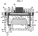
- a cylindrical wall surrounding the electrodes 111 and 120 and the processing space 107 is formed, and an outer gas exhaust path 138 for directly exhausting the processing gas introduced into the space 108 between the upper electrode 120 and the ceiling wall 105 is formed at the outside of the cylindrical wall.
- Fig. 1 shows a shield sidewall 310 of a shield member 300 serving as the cylindrical wall surrounding the electrodes 111 and 120 and the processing space 107.
- the outer gas exhaust path 138 is formed between the shield sidewall 310 and the sidewall 103 of the processing chamber 102 and serves as a gas exhaust space communicating with the gas exhaust port 132.
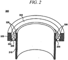
- the shield member 300 may be configured as shown in Fig. 2 , for example.
- the shield member 300 may include the shield sidewall 310 and a flange 320 attached to an upper portion of the shield sidewall 310.
- the shield sidewall 310 and the flange 320 may be formed as a single part or as separate parts.
- a groove 322 is formed at the flange 320 along the circumference of the shield sidewall 310.
- a multiple number of communication holes 326 are formed so as to allow the space 108 above the upper electrode 120 to communicate with the outer gas exhaust path 138.
- a conductance of the outer gas exhaust path 138 can be adjusted by changing the number or the shape of the communication holes 326.
- the conductance of the outer gas exhaust path 138 may be set to be greater than a conductance of a gap between the upper electrode 120 and the shield sidewall 310.
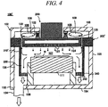
- the outer gas exhaust path 138 is not provided as shown in Fig. 4 , it may be extremely difficult to exhaust the processing gas that has been introduced into the space 108 above the upper electrode 120, and the processing gas is highly likely to remain in the space 108.
- the outer gas exhaust path 138 is provided as shown in Fig. 3 , the processing gas that has been introduced into the space 108 above the upper electrode 120 can be easily exhausted directly from the gas exhaust port 132 through the outer gas exhaust path 138. As a consequence, it is possible to prevent the processing gas from remaining in the space 108 above the upper electrode 120.
- a pressure in the space 108 above the upper electrode 120 can be maintained at a low level, so that abnormal electrical discharge can be prevented from occurring in the space 108.
- the conductance of the outer gas exhaust path 138 can be set to be greater than the conductance of the gap (gap into which the processing gas is introduced) formed around the upper electrode 120. Accordingly, the processing gas that has been introduced into the space 108 above the upper electrode 120 can be more easily exhausted from the gas exhaust port 132.
- the configuration of the shield member 300 is not limited to the example shown in Fig. 2 .
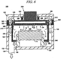
- communication holes 312 may be formed at the shield sidewall 310 so as to allow a space of the groove 322 of the flange 320 to communicate with the gap between the upper electrode 120 and the shield sidewall 310.
- the processing gas introduced into the gap formed around the upper electrode 120 can also be flown to the outer gas exhaust path 138 through the communication holes 312 and 326, as can be seen from Fig. 6 . Accordingly, the processing gas inside the shield sidewall 310 can be prevented from entering the space 108 above the upper electrode 120.
- the bypass line 350 serving as the outer exhaust path 138 in a plasma processing apparatus 100" in which the shield sidewall 310 is not installed.
- the sidewall 103 of the processing chamber 102 may serve as a cylindrical wall surrounding the electrodes 120 and 111 and the processing space 107. With this configuration, it is possible to prevent the processing gas from remaining in the space 108 above the upper electrode 120.
Description
- The present disclosure relates to a plasma processing apparatus including an upper electrode capable of vertically moving within a processing chamber.
- As for a plasma processing apparatus for manufacturing a semiconductor device, there is widely used a so-called parallel plate type plasma processing apparatus which includes a lower electrode for mounting thereon a substrate such as a semiconductor wafer, a liquid crystal substrate or the like; and an upper electrode disposed to face the lower electrode in a processing chamber. In this plasma processing apparatus, the substrate is mounted on the lower electrode, a processing gas is introduced toward the lower electrode through a multiple number of discharge holes formed in the upper electrode, and then plasma of the processing gas is generated by applying a high frequency power between the electrodes. Accordingly, a plasma process such as an etching process or a film formation process is performed on the substrate.
- In this parallel plate type plasma processing apparatus, a distance between the upper electrode and the lower electrode may affect plasma processing characteristics on the substrate. Therefore, the distance needs to be accurately adjusted depending on processing conditions or types of plasma processes. Especially, when different types of plasma processes or plasma processes having different processing conditions are continuously performed in the same processing chamber, the distance needs to be adjusted to an optimal distance for each of the plasma processes. For this reason, conventionally, there has been developed a plasma processing apparatus capable of optimally adjusting a distance between an upper electrode and a lower electrode by vertically moving the upper electrode (see, e.g., Patent Document 1).
- The plasma processing apparatus described in Patent Document 1 is configured to vertically move the upper electrode between a ceiling wall of a processing chamber and the lower electrode by installing the upper electrode at the ceiling wall of the processing chamber via a bellows. With this configuration, the distance between the upper electrode and the lower electrode (distance between electrodes) can be adjusted by vertically moving the upper electrode.
- Patent Document 1: Japanese Patent Laid-open Publication No.
2005-93843 - However, in the above-described conventional plasma processing apparatus, since the bellows is installed above the upper electrode, a gap of a certain height exists even when the bellows is contracted. Therefore, a space (space above the upper electrode) between the ceiling wall and the upper electrode is formed within the processing chamber. As a consequence, a processing gas supplied into the processing chamber may also be introduced in this space through a gap between a side surface of the upper electrode and an inner wall of the processing chamber and remain therein.
- The processing gas introduced in this space may be hardly exhausted even by driving a vacuum pump. By way of example, when the upper electrode is moved vertically or when an internal pressure of the processing chamber is controlled for a next plasma process, the processing gas remaining in this space may flow downward toward a processing space below the upper electrode. This may affect plasma processing characteristics. Further, when the processing gas is introduced into the space above the upper electrode, a pressure may be increased. Hence, abnormal electric discharge may occur in the space when a high frequency power is applied between the electrodes.
- Document
JP H03 145124 A JP H10 302998 A JP H08 199364 A US 2007/221130 A1 . - In view of the foregoing, the present disclosure provides a plasma processing apparatus capable of easily exhausting a processing gas introduced in a space above a vertically movable upper electrode, thereby preventing abnormal electrical discharge from occurring in the space above the upper electrode.
- In accordance with one aspect of the present disclosure, there is provided a plasma processing apparatus for performing a plasma process on a substrate in a processing chamber. The plasma processing apparatus includes a lower electrode installed at a bottom wall of the processing chamber and configured to mount thereon the substrate; an upper electrode installed so as to face the lower electrode and having a plurality of discharge holes for introducing a processing gas toward the substrate; a power supply unit configured to supply a high frequency power for generating plasma of the processing gas between the electrodes; an elevation unit installed at a ceiling wall of the processing chamber and configured to elevate the upper electrode between the ceiling wall and the lower electrode; a cylindrical wall configured to surround the electrodes and a processing space between the electrodes; an inner gas exhaust path formed at the inside of the cylindrical wall and configured to exhaust an atmosphere in the processing space; and an outer gas exhaust path formed at the outside of the cylindrical wall and configured to exhaust the processing gas introduced into a space between the upper electrode and the ceiling wall.
- In accordance with the present disclosure, even if the processing gas supplied into the processing space inside the cylindrical wall is introduced in the space (space above the upper electrode) between the ceiling wall and the upper electrode from the gap between the upper electrode and the cylindrical wall, the processing can be easily exhausted through a gas exhaust port via the outer gas exhaust path. Further, a pressure in the space above the upper electrode can be maintained at a low level, so that abnormal electrical discharge can be prevented from occurring in the space.
- Here, the cylindrical wall is a shield sidewall provided at the inside of a sidewall of the processing chamber, and the outer gas exhaust path may include a gas exhaust space formed between the sidewall of the processing chamber and the shield sidewall. By forming the outer gas exhaust path with the shield sidewall, the processing gas introduced into the space above the upper electrode can be effectively exhausted.
- Further, a flange protruded so as to block the outer gas exhaust path is secured to an upper portion of the shield sidewall, and the flange is provided with a plurality of communicating holes that allows the outer gas exhaust path to communicate with the space between the upper electrode and the ceiling wall. A conductance of the outer gas exhaust path may be adjusted by changing the number or the shape of the communication holes. With this configuration, a difference between the conductance of the outer gas exhaust path and a conductance of the gap between the upper electrode and the cylindrical wall can be increased. Accordingly, exhaust efficiency of the processing gas introduced into the space between the ceiling wall and the upper electrode can be improved.
- Furthermore, a groove is formed in the flange along a periphery of the shield sidewall, and the communication holes are formed in a bottom of the groove. Moreover, a plurality of communication holes is formed in the shield sidewall so as to allow a space in the groove to communicate with a gap between the upper electrode and the shield sidewall. With this configuration, the processing gas introduced into the gap between the upper electrode and the shield sidewall can flow to the gas exhaust port through the communication holes and the outer gas exhaust path. Accordingly, the processing gas can be prevented from entering the space above the upper electrode.
- Moreover, the cylindrical wall may be the sidewall of the processing chamber, and the outer gas exhaust path may be a bypass line that allows the space between the upper electrode and the ceiling wall to communicate with a gas exhaust line connected to a gas exhaust port of the processing chamber. Accordingly, the present disclosure is applicable to a plasma processing apparatus in which the shield sidewall is not installed.
- In accordance with the present disclosure, even if the processing gas is introduced into the space above the movable upper electrode, the processing gas can be easily exhausted through the outer gas exhaust path and an abnormal electrical discharge can be prevented from occurring in the space.
- Non-limiting and non-exhaustive embodiments will be described in conjunction with the accompanying drawings. Understanding that these drawings depict only several embodiments in accordance with the disclosure and are, therefore, not to be intended to limit its scope, the disclosure will be described with specificity and detail through use of the accompanying drawings, in which:
-
Fig. 1 is a cross sectional view showing a schematic configuration of a plasma processing apparatus in accordance with an embodiment of the present disclosure. -
Fig. 2 is a cross sectional perspective view showing a configuration example of a shield member shown inFig. 1 . -
Fig. 3 is a diagram for describing a gas exhaust flow within a processing chamber and is a cross sectional view showing a schematic configuration of the plasma processing apparatus in accordance with the present disclosure. -
Fig. 4 is a diagram for describing a gas exhaust flow within a processing chamber and is a cross sectional view showing a schematic configuration of a plasma processing apparatus in accordance with a comparative example. -
Fig. 5 is a cross sectional perspective view showing a modification example of the shield member in accordance with the present embodiment. -
Fig. 6 is a cross sectional view for describing a gas exhaust flow within the processing chamber of the plasma processing apparatus having the shield member shown inFig. 5 . -
Fig. 7 is a cross sectional view showing a modification example of the plasma processing apparatus in accordance with the present embodiment. -
Fig. 8 is a cross sectional view showing another modification example of the plasma processing apparatus in accordance with the present embodiment. - Hereinafter, the embodiments of the present disclosure will be described in detail with reference to the accompanying drawings. Through the present specification and drawings, parts having substantially the same function and configuration will be assigned same reference numerals, and redundant description will be omitted.
-
Fig. 1 shows a schematic configuration of a parallel plate typeplasma processing apparatus 100 as an example of a plasma processing apparatus in accordance with an embodiment of the present disclosure. Theplasma processing apparatus 100 may include acylindrical processing chamber 102 made of, e.g., aluminum whose surface is anodically oxidized (alumite treated). Theprocessing chamber 102 is electrically grounded. Theprocessing chamber 102 may have, by way of example, a processing vessel surrounded by acylindrical sidewall 103, abottom wall 104 and aceiling wall 105. Theceiling wall 105 is detachably fixed to an upper portion of thesidewall 103. - Provided within the
processing chamber 102 are a lower electrode (susceptor) 111 serving as a part of a mounting table 110 for mounting thereon a wafer W and anupper electrode 120 installed so as to face thelower electrode 111 and serving as a shower head for introducing a processing gas, a purge gas or the like. - The
lower electrode 111 is made of, e.g., aluminum and is installed at thebottom wall 104 of theprocessing chamber 102 via a cylindricalinsulating support 106. Further, thelower electrode 111 is formed in a columnar shape so as to correspond to an outer diameter of the wafer W. - Installed on a top surface of the
lower electrode 111 is anelectrostatic chuck 112 for holding the wafer W by an electrostatic attracting force. Theelectrostatic chuck 112 has anelectrostatic chuck electrode 114 made of, e.g., a conductive film embedded in an insulating film. ADC power supply 115 is electrically connected to theelectrostatic chuck electrode 114. With this configuration of theelectrostatic chuck 112, the wafer W can be attracted to and held on theelectrostatic chuck 112 by a Coulomb force generated by a DC voltage from theDC power supply 115. - A cooling unit is installed within the
lower electrode 111. By way of example, the cooling unit is configured to circulate and supply a coolant (for example, cooling water) of a predetermined temperature to acoolant path 116 extended along a circumference within thelower electrode 111 from a non-illustrated chiller unit through a coolant line. A processing temperature of the water W on theelectrostatic chuck 112 can be controlled by adjusting the temperature of the coolant. - In the lower electrode 11 and the
electrostatic chuck 112, a heat transfergas supply line 118 is provided toward a rear surface of the wafer W. A heat transfer gas (a backgas) such as a He gas is introduced through the heat transfergas supply line 118 and supplied between a top surface of theelectrostatic chuck 112 and the rear surface of the wafer W. Accordingly, a heat transfer between thelower electrode 111 and the wafer W is accelerated. Afocus ring 119 is installed so as to surround the wafer W mounted on theelectrostatic chuck 112. Thefocus ring 119 is made of, e.g., quartz or silicon and installed on the top surface of thelower electrode 111. - The
upper electrode 120 is supported at theceiling wall 105 of theprocessing chamber 102 so as to be elevatable by an upperelectrode elevation unit 200. Accordingly, a distance between thelower electrode 111 and theupper electrode 120 can be adjusted. The upperelectrode elevation unit 200 will be described in detail later. - The
upper electrode 120 is supported at theceiling wall 105 of theprocessing chamber 102 via a bellows 122. The bellows 122 is fixed to a bottom surface of an outer part of anopening 102a formed in theceiling wall 105 of theprocessing chamber 102 by a fixing member such as a bolt via aflange 122a. Further, thebellows 122 is fixed to a top surface of theupper electrode 120 by a fixing member such as a bolt via aflange 122b. - The
upper electrode 120 may include anelectrode plate 124 serving as a facing surface to thelower electrode 111 and having a multiple number of discharge holes 123; and anelectrode support 125 for supporting theelectrode plate 124. Theelectrode plate 124 is made of, e.g., quartz and theelectrode support 125 is made of, e.g., a conductive material such as aluminum whose surface is alumite treated. - The
electrode support 125 of theupper electrode 120 has agas inlet opening 126. Agas supply line 127 is connected to thegas inlet opening 126. Further, a processinggas supply unit 130 is connected to thegas supply line 127 via avalve 128 and amass flow controller 129. - By way of example, an etching gas for a plasma etching process is supplied from the processing
gas supply unit 130. Although one processing gas supply system including thegas supply line 127, thevalve 128, themass flow controller 129 and the processinggas supply unit 130 is illustrated inFig. 1 , theplasma processing apparatus 100 may have a multiple number of processing gas supply systems. By way of example, processing gases such as CHF3, Ar and He are supplied into theprocessing chamber 102 while flow rates thereof are independently controlled. - Hereinafter, a configuration example of an upper
electrode elevation unit 200 will be described with reference toFig. 1 . The configuration of the upperelectrode elevation unit 200 is not limited to that shown inFig. 1 . The upperelectrode elevation unit 200 ofFig. 1 may include a substantially cylindrical slidingsupport member 204 for supporting and slidably moving theupper electrode 120 within theprocessing chamber 102. The slidingsupport member 204 is installed substantially at a center of the upper portion of theupper electrode 120 by bolts or the like. - The sliding
support member 204 is installed such that the slidingsupport member 204 can be inserted into and retracted from theopening 102a formed substantially at a center of the ceiling wall of theprocessing chamber 102. Specifically, an outer peripheral surface of the slidingsupport member 204 is supported at a sidewall surface of theopening 102a of theprocessing chamber 102 so as to be slidable via aslide unit 210. - The
slide unit 210 may include aguide member 216 fixed to a vertical portion of a fixingmember 214 installed at an upper portion of theprocessing chamber 102 and having an L-shaped cross section; and arail member 212 slidably supported by theguide member 216 and formed in one direction (vertical direction in the present embodiment) on the outer peripheral surface of the slidingsupport member 204. - A horizontal portion of the fixing
member 214 for fixing theguide member 216 of theslide unit 210 is fixed to the upper portion of theprocessing chamber 102 via an annularhorizontality adjustment plate 218. Thehorizontality adjustment plate 218 is configured to adjust a horizontal position of theupper electrode 120. By way of example, thehorizontality adjustment plate 218 may be fixed to theprocessing chamber 102 by a multiple number of bolts spaced apart from each other at a regular interval along a periphery of thehorizontality adjustment plate 218, and an inclination of thehorizontality adjustment plate 218 with respect to a horizontal plane can be varied by adjusting a protruding degree of the bolts. By adjusting the inclination of thehorizontality adjustment plate 218 with respect to the horizontal plane, an inclination of theguide member 216 of theslide unit 210 with respect to a vertical plane can be adjusted. Since theupper electrode 120 is supported via theguide member 216, an inclination of theupper electrode 120 with respect to the horizontal plane can be adjusted resultantly. In this way, the horizontality of theupper electrode 120 can be adjusted by a simple manipulation. - An
air pressure cylinder 220 for moving theupper electrode 120 is installed above theprocessing chamber 102 via acylindrical body 201. That is, a lower end of thecylindrical body 201 is airtightly mounted so as to cover theopening 102a of theprocessing chamber 102 by bolts or the like, and an upper end of thecylindrical body 201 is airtightly secured at a lower end of theair pressure cylinder 220. - The
air pressure cylinder 220 has arod 202 capable of moving in one direction, and a lower end of therod 202 is connected to a substantially upper central portion of the slidingsupport member 204 by bolts or the like. With this configuration, by moving therod 202 of theair pressure cylinder 220, theupper electrode 120 is moved in one direction along the slide unit by the slidingsupport member 204. Therod 202 is formed in a cylindrical shape, and an inner space of therod 202 communicates with a central hole formed substantially at a center of the slidingsupport member 204 and opens to the atmosphere. Accordingly, wiring such as a grounding wire (not shown inFig. 1 ) can be connected to theupper electrode 120 through the inner space of therod 202 and the central hole of the slidingsupport member 204. - In addition, a
linear encoder 205 serving as a position detecting device for detecting a position of theupper electrode 120 is installed at a side of theair pressure cylinder 220. Meanwhile, anupper member 207 having aprotrusion 207a extending sideward from therod 202 is mounted on an upper end of therod 202 of theair pressure cylinder 220, and adetection member 205a of thelinear encoder 205 is in contact with theprotrusion 207a of theupper member 207. Since theupper member 207 is coupled with theupper electrode 120, the position of theupper electrode 120 can be detected by thelinear encoder 205. - The
air pressure cylinder 220 may include a cylindermain body 222 interposed between an upper support plate 224 and alower support plate 226. Attached to an outer peripheral surface of therod 202 is anannular partition member 208 for partitioning the inside of theair pressure cylinder 220 into afirst cylinder space 232 and asecond cylinder space 234. - Compressed air is introduced into the
first space 232 of theair pressure cylinder 220 through a non-illustrated upper port. Further, compressed air is introduced into thesecond space 234 of theair pressure cylinder 220 through a non-illustrated lower port. By controlling the amount of the air introduced into thefirst cylinder space 232 and thesecond cylinder space 234, therod 202 can be moved in one direction (here, in the vertical direction). The amount of the air introduced into theair pressure cylinder 220 is controlled by anair pressure circuit 240 installed near theair pressure cylinder 220. Although the embodiment has been described for the case of using theair pressure cylinder 220 as an actuator for vertically moving theupper electrode 120, the present disclosure is not limited thereto. - A
power supply unit 140 for supplying dual frequency powers is connected to thelower electrode 111. Thepower supply unit 140 may include a first high frequencypower supply unit 142 for supplying a first high frequency power (high frequency power for plasma excitation) of a first frequency; and a second high frequencypower supply unit 152 for supplying a second high frequency power (high frequency power for bias voltage generation) of a second frequency lower than the first frequency. - The first high frequency
power supply unit 142 may include afirst filter 144, afirst matching unit 146 and afirst power supply 148 connected in sequence from thelower electrode 111. Thefirst filter 144 prevents a power component of the second frequency from entering thefirst matching unit 146. Thefirst matching unit 146 matches a component of the first high frequency power. - The second high frequency
power supply unit 152 may include asecond filter 154, asecond matching unit 156 and asecond power supply 158 connected in sequence from thelower electrode 111. Thesecond filter 154 prevents a power component of the first frequency from entering thesecond matching unit 156. Thesecond matching unit 156 matches a component of the second high frequency power. - A controller (overall control unit) 160 is connected to the
plasma processing apparatus 100. Each part of theplasma processing apparatus 100 is controlled by thecontroller 160. Further, thecontroller 160 is connected to amanipulation unit 162 including a keyboard through which an operator inputs commands to manage theplasma processing apparatus 100 or a display which visually displays an operation status of theplasma processing apparatus 100. - Further, the
controller 160 is connected to astorage unit 164 that stores therein: programs for implementing various processes (e.g., etching, ashing, or film formation) performed in theplasma processing apparatus 100 under the control of thecontroller 160; and processing conditions (recipes) required for executing the programs. - By way of example, the
storage unit 160 stores a multiple number of processing conditions (recipes). Each processing condition includes a multiple number of parameter values such as control parameters for controlling each part of theplasma processing apparatus 100 and setting parameters. Each processing condition may include parameter values such as a flow rate ratio of the processing gases, a pressure in the processing chamber, a high frequency power, and the like. - Further, the programs or the processing conditions may be stored in a hard disk or a semiconductor memory, or may be set at a predetermined area of the
storage unit 164 in the form of a storage medium readable by a portable computer such as a CD-ROM, a DVD, or the like. - The
controller 160 reads out a program and processing condition from thestorage unit 164 in response to an instruction from themanipulation unit 162 and controls each part, thereby carrying out a desired process in theplasma processing apparatus 100. Further, the processing condition can be edited by themanipulation unit 162. - A
gas exhaust port 132 is formed at thebottom wall 104 of theprocessing chamber 102. Agas exhaust unit 136 is connected to thegas exhaust port 132 via agas exhaust line 134. Thegas exhaust unit 136 includes, e.g., a vacuum pump and is capable of depressurizing the inside of theprocessing chamber 102 to a preset vacuum degree. Further, although not shown, a loading/unloading port for the wafer W and a gate valve for opening/closing the loading/unloading port are provided at thesidewall 103 of theprocessing chamber 102. - In this
plasma processing apparatus 100, a distance between electrodes is adjusted by vertically moving theupper electrode 120. Further, the processing gas is introduced toward aprocessing space 107 above the lower electrode via theupper electrode 120 from the processinggas supply unit 130, and the first and the second high frequency powers are applied to thelower electrode 111. Accordingly, plasma of the processing gas is generated and a plasma process such as etching or film formation is performed on the wafer W mounted on the mounting table 110. - However, in this
plasma processing apparatus 100 having the vertically movableupper electrode 120, since thebellows 122 is mounted on the upper electrode 120 (on the electrode support 125), a gap of a certain height exists even when thebellows 122 is contracted. Accordingly, outside thebellows 122, aspace 108 is formed between theceiling wall 105 and the upper electrode 120 (space between theceiling wall 105 and the electrode support 125). As a consequence, the processing gas introduced into thespace 108 through a gap formed around the side portion of theupper electrode 120 may remain in thespace 108. Here, if the gap formed around theupper electrode 120 is small, it is difficult to exhaust the remaining processing gas through thegas exhaust port 132 even by driving the vacuum pump. - Hence, in the present embodiment, a cylindrical wall surrounding the
electrodes processing space 107 is formed, and an outergas exhaust path 138 for directly exhausting the processing gas introduced into thespace 108 between theupper electrode 120 and theceiling wall 105 is formed at the outside of the cylindrical wall.Fig. 1 shows ashield sidewall 310 of ashield member 300 serving as the cylindrical wall surrounding theelectrodes processing space 107. Here, the outergas exhaust path 138 is formed between theshield sidewall 310 and thesidewall 103 of theprocessing chamber 102 and serves as a gas exhaust space communicating with thegas exhaust port 132. - With this configuration, when the vacuum pump of the
gas exhaust unit 136 is driven, the processing gas introduced into thespace 108 above theupper electrode 120 is directly exhausted through thegas exhaust port 132 via the outergas exhaust path 138. By forming the outergas exhaust path 138 with theshield sidewall 310, the processing gas introduced into thespace 108 above theupper electrode 120 can be effectively exhausted. - The
shield member 300 may be configured as shown inFig. 2 , for example. Theshield member 300 may include theshield sidewall 310 and aflange 320 attached to an upper portion of theshield sidewall 310. Here, theshield sidewall 310 and theflange 320 may be formed as a single part or as separate parts. - The
shield member 300 is supported at an upper portion of thesidewall 103 of theprocessing chamber 102 by theflange 320. Specifically, theflange 320 is protruded outward from an outer peripheral surface of theshield sidewall 310 so as to block the outergas exhaust path 138. As shown inFig. 1 , theflange 320 is secured between thesidewall 103 and theceiling wall 105 by bolts or the like. A sealing member such as a non-illustrated O-ring is provided at theflange 320 in order to maintain airtightness between theflange 320 and thesidewall 103 of theprocessing chamber 102 and between theflange 320 and theceiling wall 105 of theprocessing chamber 102. - As shown in
Fig. 2 , agroove 322 is formed at theflange 320 along the circumference of theshield sidewall 310. At abottom 324 of thegroove 322, a multiple number ofcommunication holes 326 are formed so as to allow thespace 108 above theupper electrode 120 to communicate with the outergas exhaust path 138. A conductance of the outergas exhaust path 138 can be adjusted by changing the number or the shape of the communication holes 326. Here, in order to increase exhaust efficiency through the outergas exhaust path 138, desirably, the conductance of the outergas exhaust path 138 may be set to be greater than a conductance of a gap between theupper electrode 120 and theshield sidewall 310. - Although the
communication hole 326 is described to have a round shape inFig. 2 , the shape of thecommunication hole 326 is not limited thereto. Thecommunication hole 326 may have another shape such as a slit shape, an elliptical shape or the like. When thecommunication hole 326 is a slit, thecommunication hole 326 may extend in a radial direction or in a circumferential direction. In this way, simply by adjusting the number or the shape of the communication holes 326, a difference between the conductance of the outergas exhaust path 138 and the conductance of the gap between theupper electrode 120 and theshield sidewall 310 can be increased. Accordingly, the processing gas introduced into thespace 108 above theupper electrode 120 can be exhausted more effectively. - An inner
gas exhaust path 330 communicating with thegas exhaust port 132 is formed inside theshield sidewall 310, i.e., between theshield sidewall 310 and thecylindrical support 106. Abaffle plate 340 is secured between the innergas exhaust path 330 and thegas exhaust port 132. Specifically, by way of example, thebaffle plate 340 is attached to a lower end of theshield sidewall 310 so as to surround thecylindrical support 106, as can be seen fromFig. 1 . A multiple number of throughholes 342 are formed in thebaffle plate 340. Hence, when the vacuum pump of thegas exhaust unit 136 is driven, the atmosphere in theshield sidewall 310 is exhausted from thegas exhaust port 132 through the innergas exhaust path 330 and the throughholes 342 of thebaffle plate 340. - An inner surface of the
shield sidewall 310 is anodically oxidized (e.g., alumite treated) and, thus, particles hardly adhere thereto. By surrounding theprocessing space 107 with thisshield sidewall 310, thesidewall 103 of theprocessing chamber 102 can be protected from particles and the like. - Next, a gas exhaust flow in the
plasma processing apparatus 100 will be described with reference to the following drawings.Fig. 3 is a schematic cross sectional view of theplasma processing apparatus 100 in which theshield member 300 forming the outergas exhaust path 138 is installed.Fig. 4 is a schematic cross sectional view of a plasma processing apparatus 100' in accordance with a comparative example and the plasma processing apparatus 100' in which a shield member 300' without forming an outergas exhaust path 138 is installed. InFigs. 3 and4 , the illustration of the configuration of the upperelectrode elevation unit 200 and the configuration near thelower electrode 111 is simplified. - In both apparatuses shown in
Figs. 3 and4 , when the vacuum pump of thegas exhaust unit 136 ofFig. 1 is driven, the processing gas is introduced from theupper electrode 120 toward theprocessing space 107. If the first and second high frequency powers are applied to the lower electrode, plasma of the processing gas is generated and a plasma process is performed on the wafer W. - Here, most of the atmosphere in the shield sidewalls 310 and 310' is exhausted through the
gas exhaust port 132 via the innergas exhaust path 330 and the throughholes 342 of thebaffle plate 340. Meanwhile, a part of the atmosphere in thesidewalls 310 and 310' is introduced into thespace 108 above theupper electrode 120 through the gap formed around the side portion of theupper electrode 120. Therefore, theprocessing gas 109 is introduced into thespace 108 above theupper electrode 120. - In this case, if the outer
gas exhaust path 138 is not provided as shown inFig. 4 , it may be extremely difficult to exhaust the processing gas that has been introduced into thespace 108 above theupper electrode 120, and the processing gas is highly likely to remain in thespace 108. On the contrary, if the outergas exhaust path 138 is provided as shown inFig. 3 , the processing gas that has been introduced into thespace 108 above theupper electrode 120 can be easily exhausted directly from thegas exhaust port 132 through the outergas exhaust path 138. As a consequence, it is possible to prevent the processing gas from remaining in thespace 108 above theupper electrode 120. Besides, a pressure in thespace 108 above theupper electrode 120 can be maintained at a low level, so that abnormal electrical discharge can be prevented from occurring in thespace 108. - In addition, by adjusting the number or the shape of the communication holes 326 of the
shield sidewall 310, the conductance of the outergas exhaust path 138 can be set to be greater than the conductance of the gap (gap into which the processing gas is introduced) formed around theupper electrode 120. Accordingly, the processing gas that has been introduced into thespace 108 above theupper electrode 120 can be more easily exhausted from thegas exhaust port 132. - Further, the configuration of the
shield member 300 is not limited to the example shown inFig. 2 . By way of example, as shown inFig. 5 , communication holes 312 may be formed at theshield sidewall 310 so as to allow a space of thegroove 322 of theflange 320 to communicate with the gap between theupper electrode 120 and theshield sidewall 310. With this configuration, the processing gas introduced into the gap formed around theupper electrode 120 can also be flown to the outergas exhaust path 138 through the communication holes 312 and 326, as can be seen fromFig. 6 . Accordingly, the processing gas inside theshield sidewall 310 can be prevented from entering thespace 108 above theupper electrode 120. - The number or the shape of the communication holes 312 is not limited to the example illustrated in
Fig. 5. Fig. 5 shows thecommunication hole 312 having a round shape. However, thecommunication hole 312 may have another shape such as a slit shape, an elliptical shape or the like. When thecommunication hole 312 is formed in a slit shape, thecommunication hole 312 may extend in a radial direction or in a circumferential direction. - In the above-described embodiment, although the
shield sidewall 310 is configured as the cylindrical wall surrounding theelectrodes processing space 107 and the outergas exhaust path 138 is formed between theshield sidewall 310 and thesidewall 103 of theprocessing chamber 102, the present disclosure is not limited thereto. By way of example, as shown inFig. 7 , the outergas exhaust path 138 may be implemented by a bypass line that allows thespace 108 above theupper electrode 120 to communicate with thegas exhaust line 134 of theprocessing chamber 102. -
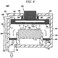
Fig. 7 shows an example configuration in which abypass line 350 serving as the outergas exhaust path 138 is installed in the plasma processing apparatus 100' ofFig. 4 . In this example, the processing gas introduced in thespace 108 above theupper electrode 120 can be easily exhausted directly from thegas exhaust port 132 through thebypass line 350 serving as the outergas exhaust path 138. With this configuration, it is possible to prevent the processing gas from remaining in thespace 108 above theupper electrode 120. - Further, as shown in
Fig. 8 , it is also possible to use thebypass line 350 serving as theouter exhaust path 138 in aplasma processing apparatus 100" in which theshield sidewall 310 is not installed. In this case, thesidewall 103 of theprocessing chamber 102 may serve as a cylindrical wall surrounding theelectrodes processing space 107. With this configuration, it is possible to prevent the processing gas from remaining in thespace 108 above theupper electrode 120. - While various aspects and embodiments have been described herein, other aspects and embodiments will be apparent to those skilled in the art. The various aspects and embodiments disclosed herein are for the purposes of illustration and are not intended to be limiting. Therefore, the true scope of the disclosure is indicated by the appended claims rather than by the foregoing description, and it shall be understood that all modifications and embodiments conceived from the meaning and scope of the claims and their equivalents are included in the scope of the disclosure.
- Although the embodiment of the present disclosure has been described for the plasma processing apparatus that generates plasma by applying two kinds of high frequency powers to the lower electrode, the present disclosure is not limited thereto. By way of example, the present disclosure is applicable to other types of plasma processing apparatuses such as a type that applies one kind of high frequency power to the lower electrode or a type that applies two kinds of high frequency powers to the upper electrode and the lower electrode respectively.
- The present disclosure is applicable to a plasma processing apparatus having a vertically movable upper electrode within a processing chamber. The invention is defined by the claims.
Claims (3)
- A plasma processing apparatus (100) for performing a plasma process on a substrate (W) in a processing chamber (102), the apparatus (100) comprising:the processing chamber (102);a lower electrode (111) installed at a bottom wall (104) of the processing chamber (102) and configured to mount thereon the substrate (W);an upper electrode (120) installed so as to face the lower electrode (111) and having a plurality of discharge holes (123) for introducing, in use, a processing gas toward the substrate (W);a power supply unit (140) configured to supply a high frequency power such that, in use, a plasma of the processing gas is generated between the electrodes (111, 120);a shield sidewall (310) Provided at the inside of the sidewall of the processing chamber (102), and configured to surround the electrodes (111, 120) and a processing space (107) between the electrodes (111, 120);an inner gas exhaust path (330) formed at the inside of the shield sidewall (310) and configured to exhaust, in use, an atmosphere in the processing space (107); andan outer gas exhaust path (138) formed at the outside of the shield sidewall (310), configured to exhaust, in use, the processing gas introduced into a space between the upper electrode (120) and a ceiling wall (105) of the processing chamber (102), and including a gas exhaust space formed between the sidewall of the processing chamber (102) and the shield sidewall (310), characterized byan elevation unit (200) installed at the ceiling wall (105) of the processing chamber (102) and configured to elevate the upper electrode (120) between the ceiling wall (105) and the lower electrode (111),wherein a flange (320) protruded so as to block the outer gas exhaust path (138) is secured to an upper portion of the shield sidewall (310),wherein a groove (322) is formed in the flange (320) along a periphery of the shield sidewall (310),wherein a plurality of first communication holes (326) is formed in a bottom of the groove (322) so as to allow the outer gas exhaust path (138) to communicate with the space between the upper electrode (120) and the ceiling wall (105), andwherein a plurality of second communication holes (312) is formed in the shield sidewall (310) so as to allow a space in the groove (322) to communicate with a gap between the upper electrode (120) and the shield sidewall (310).
- A plasma processing apparatus (100) for performing a plasma process on a substrate (W) in a processing chamber (102), the apparatus (100) comprising:the processing chamber (102);a lower electrode (111) installed at a bottom wall (104) of the processing chamber (102) and configured to mount thereon the substrate (W);an upper electrode (120) installed so as to face the lower electrode (111) and having a plurality of discharge holes (123) for introducing, in use, a processing gas toward the substrate (W);a power supply unit (140) configured to supply a high frequency power such that, in use, a plasma of the processing gas is generated between the electrodes (111, 120);a shield sidewall (310) provided at the inside of the sidewall of the processing chamber (102), and configured to surround the electrodes (111, 120) and a processing space (107) between the electrodes (111, 120);an inner gas exhaust path (330) formed at the inside of the shield sidewall (310) and configured to exhaust, in use, an atmosphere in the processing space (107); andan outer gas exhaust path (138) formed at the outside of the shield sidewall (310), configured to exhaust, in use, the processing gas introduced into a space between the upper electrode (120) and a ceiling wall (105) of the processing chamber (102), and including a gas exhaust space formed between the sidewall of the processing chamber (102) and the shield sidewall (310), characterized byan elevation unit (200) installed at the ceiling wall (105) of the processing chamber (102) and configured to elevate the upper electrode (120) between the ceiling wall (105) and the lower electrode (111),wherein a flange (320) protruded so as to block the outer gas exhaust path (138) is secured to an upper portion of the shield sidewall (310),the flange (320) is provided with a plurality of communication holes (326) arranged to allow the outer gas exhaust path (138) to communicate with the space between the upper electrode (120) and the ceiling wall (105), andwherein the communication holes (326) are arranged such that their number or their shape may be changed so as to adjust a conductance of the outer gas exhaust path (138).
- A plasma processing apparatus (100) for performing a plasma process on a substrate (W) in a processing chamber (102), the apparatus (100) comprising:the processing chamber (102);a lower electrode (111) installed at a bottom wall (104) of the processing chamber (102) and configured to mount thereon the substrate (W);an upper electrode (120) installed so as to face the lower electrode (111) and having a plurality of discharge holes (123) for introducing, in use, a processing gas toward the substrate (W);a power supply unit (140) configured to supply a high frequency power such that, in use, a plasma of the processing gas is generated between the electrodes (111, 120);a cylindrical wall (310) configured to surround the electrodes (111, 120) and a processing space (107) between the electrodes (111, 120);an inner gas exhaust path (330) formed at the inside of the cylindrical wall (310) and configured to exhaust, in use, an atmosphere in the processing space (107); andan outer gas exhaust path (138) formed at the outside of the cylindrical wall (310) and configured to exhaust, in use, the processing gas introduced into a space between the upper electrode (120) and a ceiling wall (105) of the processing chamber (102),
characterized byan elevation unit (200) installed at the ceiling wall (105) of the processing chamber (102) and configured to elevate the upper electrode (120) between the ceiling wall (105) and the lower electrode (111),wherein the cylindrical wall (310) is the sidewall of the processing chamber (102), andthe outer gas exhaust path (138) is a bypass line arranged to allow the space between the upper electrode (120) and the ceiling wall (105) to communicate with a gas exhaust line (134) connected to a gas exhaust port (132) of the processing chamber (102).
Applications Claiming Priority (1)
| Application Number | Priority Date | Filing Date | Title |
|---|---|---|---|
| JP2010119547A JP5567392B2 (en) | 2010-05-25 | 2010-05-25 | Plasma processing equipment |
Publications (3)
| Publication Number | Publication Date |
|---|---|
| EP2390897A2 EP2390897A2 (en) | 2011-11-30 |
| EP2390897A3 EP2390897A3 (en) | 2014-04-30 |
| EP2390897B1 true EP2390897B1 (en) | 2019-08-21 |
Family
ID=44117156
Family Applications (1)
| Application Number | Title | Priority Date | Filing Date |
|---|---|---|---|
| EP11004262.9A Active EP2390897B1 (en) | 2010-05-25 | 2011-05-24 | Plasma processing apparatus |
Country Status (6)
| Country | Link |
|---|---|
| US (1) | US8858754B2 (en) |
| EP (1) | EP2390897B1 (en) |
| JP (1) | JP5567392B2 (en) |
| KR (1) | KR101737014B1 (en) |
| CN (1) | CN102262999B (en) |
| TW (1) | TWI522014B (en) |
Families Citing this family (70)
| Publication number | Priority date | Publication date | Assignee | Title |
|---|---|---|---|---|
| JP5445252B2 (en) * | 2010-03-16 | 2014-03-19 | 東京エレクトロン株式会社 | Deposition equipment |
| JP5567392B2 (en) * | 2010-05-25 | 2014-08-06 | 東京エレクトロン株式会社 | Plasma processing equipment |
| US8906160B2 (en) * | 2010-12-23 | 2014-12-09 | Intermolecular, Inc. | Vapor based processing system with purge mode |
| JP5902896B2 (en) * | 2011-07-08 | 2016-04-13 | 東京エレクトロン株式会社 | Substrate processing equipment |
| TWI719473B (en) | 2011-10-05 | 2021-02-21 | 美商應用材料股份有限公司 | Symmetric plasma process chamber |
| US9082590B2 (en) | 2012-07-20 | 2015-07-14 | Applied Materials, Inc. | Symmetrical inductively coupled plasma source with side RF feeds and RF distribution plates |
| US9896769B2 (en) | 2012-07-20 | 2018-02-20 | Applied Materials, Inc. | Inductively coupled plasma source with multiple dielectric windows and window-supporting structure |
| US9928987B2 (en) | 2012-07-20 | 2018-03-27 | Applied Materials, Inc. | Inductively coupled plasma source with symmetrical RF feed |
| US10170279B2 (en) | 2012-07-20 | 2019-01-01 | Applied Materials, Inc. | Multiple coil inductively coupled plasma source with offset frequencies and double-walled shielding |
| US9449794B2 (en) | 2012-07-20 | 2016-09-20 | Applied Materials, Inc. | Symmetrical inductively coupled plasma source with side RF feeds and spiral coil antenna |
| US10249470B2 (en) | 2012-07-20 | 2019-04-02 | Applied Materials, Inc. | Symmetrical inductively coupled plasma source with coaxial RF feed and coaxial shielding |
| US9132436B2 (en) | 2012-09-21 | 2015-09-15 | Applied Materials, Inc. | Chemical control features in wafer process equipment |
| JP2014082354A (en) * | 2012-10-17 | 2014-05-08 | Hitachi High-Technologies Corp | Plasma processing apparatus |
| US10256079B2 (en) | 2013-02-08 | 2019-04-09 | Applied Materials, Inc. | Semiconductor processing systems having multiple plasma configurations |
| JP6359627B2 (en) | 2013-03-15 | 2018-07-18 | アプライド マテリアルズ インコーポレイテッドApplied Materials,Incorporated | Plasma reactor with highly symmetric quadruple gas injection |
| JP2015090916A (en) * | 2013-11-06 | 2015-05-11 | 東京エレクトロン株式会社 | Substrate processing apparatus and substrate processing method |
| CN103646841B (en) * | 2013-11-22 | 2016-01-27 | 上海华力微电子有限公司 | A kind of plasma etch apparatus |
| KR101560623B1 (en) * | 2014-01-03 | 2015-10-15 | 주식회사 유진테크 | Substrate processing apparatus and substrate processing method |
| US9852905B2 (en) * | 2014-01-16 | 2017-12-26 | Taiwan Semiconductor Manufacturing Company, Ltd. | Systems and methods for uniform gas flow in a deposition chamber |
| JP2015142016A (en) * | 2014-01-29 | 2015-08-03 | 東京エレクトロン株式会社 | substrate processing apparatus |
| JP6438320B2 (en) * | 2014-06-19 | 2018-12-12 | 東京エレクトロン株式会社 | Plasma processing equipment |
| US11637002B2 (en) | 2014-11-26 | 2023-04-25 | Applied Materials, Inc. | Methods and systems to enhance process uniformity |
| JP6423706B2 (en) * | 2014-12-16 | 2018-11-14 | 東京エレクトロン株式会社 | Plasma processing equipment |
| US20160225652A1 (en) | 2015-02-03 | 2016-08-04 | Applied Materials, Inc. | Low temperature chuck for plasma processing systems |
| US10167552B2 (en) * | 2015-02-05 | 2019-01-01 | Lam Research Ag | Spin chuck with rotating gas showerhead |
| US9741593B2 (en) | 2015-08-06 | 2017-08-22 | Applied Materials, Inc. | Thermal management systems and methods for wafer processing systems |
| US10504700B2 (en) | 2015-08-27 | 2019-12-10 | Applied Materials, Inc. | Plasma etching systems and methods with secondary plasma injection |
| US10157755B2 (en) * | 2015-10-01 | 2018-12-18 | Lam Research Corporation | Purge and pumping structures arranged beneath substrate plane to reduce defects |
| US10763082B2 (en) * | 2016-03-04 | 2020-09-01 | Taiwan Semiconductor Manufacturing Co., Ltd. | Chamber of plasma system, liner for plasma system and method for installing liner to plasma system |
| US10600621B2 (en) * | 2016-03-30 | 2020-03-24 | Tokyo Electron Limited | Plasma electrode and plasma processing device |
| JP6394641B2 (en) * | 2016-04-25 | 2018-09-26 | トヨタ自動車株式会社 | Plasma device |
| US10504754B2 (en) | 2016-05-19 | 2019-12-10 | Applied Materials, Inc. | Systems and methods for improved semiconductor etching and component protection |
| KR102553629B1 (en) * | 2016-06-17 | 2023-07-11 | 삼성전자주식회사 | Plasma processing apparatus |
| US10546729B2 (en) | 2016-10-04 | 2020-01-28 | Applied Materials, Inc. | Dual-channel showerhead with improved profile |
| CN106373868B (en) * | 2016-10-10 | 2020-03-10 | 昆山龙腾光电股份有限公司 | Manufacturing method of array substrate |
| US10559451B2 (en) * | 2017-02-15 | 2020-02-11 | Applied Materials, Inc. | Apparatus with concentric pumping for multiple pressure regimes |
| USD837754S1 (en) * | 2017-04-28 | 2019-01-08 | Applied Materials, Inc. | Plasma chamber liner |
| USD842259S1 (en) * | 2017-04-28 | 2019-03-05 | Applied Materials, Inc. | Plasma chamber liner |
| USD838681S1 (en) * | 2017-04-28 | 2019-01-22 | Applied Materials, Inc. | Plasma chamber liner |
| US11276590B2 (en) | 2017-05-17 | 2022-03-15 | Applied Materials, Inc. | Multi-zone semiconductor substrate supports |
| US11276559B2 (en) | 2017-05-17 | 2022-03-15 | Applied Materials, Inc. | Semiconductor processing chamber for multiple precursor flow |
| US10297458B2 (en) | 2017-08-07 | 2019-05-21 | Applied Materials, Inc. | Process window widening using coated parts in plasma etch processes |
| JP6896565B2 (en) * | 2017-08-25 | 2021-06-30 | 東京エレクトロン株式会社 | Inner wall and substrate processing equipment |
| US11670490B2 (en) * | 2017-09-29 | 2023-06-06 | Taiwan Semiconductor Manufacturing Co., Ltd. | Integrated circuit fabrication system with adjustable gas injector |
| US11328909B2 (en) | 2017-12-22 | 2022-05-10 | Applied Materials, Inc. | Chamber conditioning and removal processes |
| WO2019146456A1 (en) * | 2018-01-26 | 2019-08-01 | 東京エレクトロン株式会社 | Substrate processing apparatus |
| US10964512B2 (en) | 2018-02-15 | 2021-03-30 | Applied Materials, Inc. | Semiconductor processing chamber multistage mixing apparatus and methods |
| US10319600B1 (en) | 2018-03-12 | 2019-06-11 | Applied Materials, Inc. | Thermal silicon etch |
| US10699879B2 (en) * | 2018-04-17 | 2020-06-30 | Applied Materials, Inc. | Two piece electrode assembly with gap for plasma control |
| CN108588818A (en) * | 2018-04-17 | 2018-09-28 | 陕西飞米企业管理合伙企业(有限合伙) | A kind of exhaust collection ring in vapor deposition equipment |
| KR102516885B1 (en) * | 2018-05-10 | 2023-03-30 | 삼성전자주식회사 | Deposition equipment and method of fabricating semiconductor device using the same |
| CN108987235B (en) * | 2018-07-12 | 2020-06-05 | 昆山龙腾光电股份有限公司 | Plasma processing device |
| US11049755B2 (en) | 2018-09-14 | 2021-06-29 | Applied Materials, Inc. | Semiconductor substrate supports with embedded RF shield |
| US11062887B2 (en) | 2018-09-17 | 2021-07-13 | Applied Materials, Inc. | High temperature RF heater pedestals |
| US11417534B2 (en) | 2018-09-21 | 2022-08-16 | Applied Materials, Inc. | Selective material removal |
| US11682560B2 (en) | 2018-10-11 | 2023-06-20 | Applied Materials, Inc. | Systems and methods for hafnium-containing film removal |
| CN109195297B (en) * | 2018-10-23 | 2020-09-18 | 山东大学 | Dielectric barrier discharge device and method capable of being precisely adjusted |
| US11121002B2 (en) | 2018-10-24 | 2021-09-14 | Applied Materials, Inc. | Systems and methods for etching metals and metal derivatives |
| US11437242B2 (en) | 2018-11-27 | 2022-09-06 | Applied Materials, Inc. | Selective removal of silicon-containing materials |
| WO2020146047A1 (en) * | 2019-01-08 | 2020-07-16 | Applied Materials, Inc. | Pumping apparatus and method for substrate processing chambers |
| JP2020147795A (en) * | 2019-03-13 | 2020-09-17 | 東京エレクトロン株式会社 | Plasma treatment apparatus |
| CN112309807B (en) * | 2019-08-02 | 2022-12-30 | 中微半导体设备(上海)股份有限公司 | Plasma etching equipment |
| CN112447474B (en) * | 2019-09-04 | 2022-11-04 | 中微半导体设备(上海)股份有限公司 | Plasma processor with movable ring |
| JP7378276B2 (en) | 2019-11-12 | 2023-11-13 | 東京エレクトロン株式会社 | plasma processing equipment |
| JP7422531B2 (en) | 2019-12-17 | 2024-01-26 | 東京エレクトロン株式会社 | Plasma processing equipment and plasma processing method |
| US20220051912A1 (en) * | 2020-08-12 | 2022-02-17 | Taiwan Semiconductor Manufacturing Company Limited | Gas flow control during semiconductor fabrication |
| US20220084845A1 (en) * | 2020-09-17 | 2022-03-17 | Applied Materials, Inc. | High conductance process kit |
| US11427910B2 (en) * | 2020-10-20 | 2022-08-30 | Sky Tech Inc. | Atomic layer deposition equipment capable of reducing precursor deposition and atomic layer deposition process method using the same |
| CN114582691A (en) * | 2020-11-18 | 2022-06-03 | 中微半导体设备(上海)股份有限公司 | Plasma processing device and adjusting method thereof |
| JP2022155065A (en) * | 2021-03-30 | 2022-10-13 | 東京エレクトロン株式会社 | Substrate processing apparatus and substrate processing method |
Family Cites Families (79)
| Publication number | Priority date | Publication date | Assignee | Title |
|---|---|---|---|---|
| BE628052A (en) * | 1962-03-15 | |||
| JPS6289330A (en) * | 1985-10-16 | 1987-04-23 | Hitachi Ltd | Processor |
| KR970003885B1 (en) * | 1987-12-25 | 1997-03-22 | 도오교오 에레구토론 가부시끼 가이샤 | Etching method and apparatus thereof |
| JPH0246723A (en) * | 1988-08-09 | 1990-02-16 | Fujitsu Ltd | Device for thin film formation |
| DE3914065A1 (en) * | 1989-04-28 | 1990-10-31 | Leybold Ag | DEVICE FOR CARRYING OUT PLASMA ETCHING PROCESSES |
| US5084125A (en) * | 1989-09-12 | 1992-01-28 | Matsushita Electric Industrial Co., Ltd. | Apparatus and method for producing semiconductor substrate |
| JPH03145124A (en) * | 1989-10-31 | 1991-06-20 | Fujitsu Ltd | Dry etching device |
| DE4025396A1 (en) * | 1990-08-10 | 1992-02-13 | Leybold Ag | DEVICE FOR PRODUCING A PLASMA |
| JP2939355B2 (en) * | 1991-04-22 | 1999-08-25 | 東京エレクトロン株式会社 | Plasma processing equipment |
| FR2682047B1 (en) * | 1991-10-07 | 1993-11-12 | Commissariat A Energie Atomique | GAS PHASE CHEMICAL PROCESSING REACTOR. |
| US5238532A (en) * | 1992-02-27 | 1993-08-24 | Hughes Aircraft Company | Method and apparatus for removal of subsurface damage in semiconductor materials by plasma etching |
| US5376224A (en) * | 1992-02-27 | 1994-12-27 | Hughes Aircraft Company | Method and apparatus for non-contact plasma polishing and smoothing of uniformly thinned substrates |
| US5292400A (en) * | 1992-03-23 | 1994-03-08 | Hughes Aircraft Company | Method and apparatus for producing variable spatial frequency control in plasma assisted chemical etching |
| US5372674A (en) * | 1993-05-14 | 1994-12-13 | Hughes Aircraft Company | Electrode for use in a plasma assisted chemical etching process |
| JP3452617B2 (en) * | 1993-12-10 | 2003-09-29 | 真空冶金株式会社 | Gas deposition equipment |
| TW295677B (en) * | 1994-08-19 | 1997-01-11 | Tokyo Electron Co Ltd | |
| JPH08199364A (en) * | 1995-01-27 | 1996-08-06 | Kokusai Electric Co Ltd | Cvd apparatus and its treatment |
| TW323387B (en) * | 1995-06-07 | 1997-12-21 | Tokyo Electron Co Ltd | |
| JP3536585B2 (en) * | 1997-04-25 | 2004-06-14 | 松下電器産業株式会社 | Workpiece plasma processing apparatus and plasma processing method |
| JP2000349078A (en) * | 1999-06-03 | 2000-12-15 | Mitsubishi Electric Corp | Chemical vapor deposition apparatus and manufacture thereof |
| JP3662779B2 (en) * | 1999-06-22 | 2005-06-22 | シャープ株式会社 | Plasma processing equipment |
| JP2001057359A (en) * | 1999-08-17 | 2001-02-27 | Tokyo Electron Ltd | Plasma processing device |
| CN1199247C (en) * | 2000-05-17 | 2005-04-27 | 东京毅力科创株式会社 | Processing device and method of maintaining device, mechanism and method for assembling processing device part, and lock mechanism and method for locking the lock mechanism |
| JP3667202B2 (en) * | 2000-07-13 | 2005-07-06 | 株式会社荏原製作所 | Substrate processing equipment |
| JP4602532B2 (en) * | 2000-11-10 | 2010-12-22 | 東京エレクトロン株式会社 | Plasma processing equipment |
| KR100516844B1 (en) * | 2001-01-22 | 2005-09-26 | 동경 엘렉트론 주식회사 | Device and method for treatment |
| JP4672169B2 (en) * | 2001-04-05 | 2011-04-20 | キヤノンアネルバ株式会社 | Plasma processing equipment |
| US6527911B1 (en) * | 2001-06-29 | 2003-03-04 | Lam Research Corporation | Configurable plasma volume etch chamber |
| US20030024900A1 (en) * | 2001-07-24 | 2003-02-06 | Tokyo Electron Limited | Variable aspect ratio plasma source |
| KR100431660B1 (en) * | 2001-07-24 | 2004-05-17 | 삼성전자주식회사 | Dry Etching Apparatus for Manufacturing Semiconductor Devices |
| US20030042227A1 (en) * | 2001-08-29 | 2003-03-06 | Tokyo Electron Limited | Apparatus and method for tailoring an etch profile |
| JP4137419B2 (en) | 2001-09-28 | 2008-08-20 | 東京エレクトロン株式会社 | Plasma processing equipment |
| US20030092278A1 (en) * | 2001-11-13 | 2003-05-15 | Fink Steven T. | Plasma baffle assembly |
| JP4186536B2 (en) * | 2002-07-18 | 2008-11-26 | 松下電器産業株式会社 | Plasma processing equipment |
| KR100426816B1 (en) * | 2002-07-31 | 2004-04-14 | 삼성전자주식회사 | Plasma processing equipment having improved vacuum pressure control apparatus |
| CN1249789C (en) * | 2002-11-28 | 2006-04-05 | 东京毅力科创株式会社 | Plasma processing container internal parts |
| US7009281B2 (en) * | 2003-03-14 | 2006-03-07 | Lam Corporation | Small volume process chamber with hot inner surfaces |
| JP4173389B2 (en) * | 2003-03-19 | 2008-10-29 | 東京エレクトロン株式会社 | Plasma processing equipment |
| JP4286576B2 (en) | 2003-04-25 | 2009-07-01 | 東京エレクトロン株式会社 | Plasma processing equipment |
| US20040261712A1 (en) * | 2003-04-25 | 2004-12-30 | Daisuke Hayashi | Plasma processing apparatus |
| JP4399219B2 (en) | 2003-09-19 | 2010-01-13 | 東京エレクトロン株式会社 | Plasma processing apparatus and upper electrode unit |
| JP4399206B2 (en) * | 2003-08-06 | 2010-01-13 | 株式会社アルバック | Thin film manufacturing equipment |
| JP4607517B2 (en) * | 2003-09-03 | 2011-01-05 | 東京エレクトロン株式会社 | Plasma processing equipment |
| KR100856159B1 (en) | 2004-05-27 | 2008-09-03 | 도쿄엘렉트론가부시키가이샤 | Substrate processing apparatus |
| US20060000552A1 (en) * | 2004-07-05 | 2006-01-05 | Tokyo Electron Limited | Plasma processing apparatus and cleaning method thereof |
| US7708834B2 (en) * | 2004-11-02 | 2010-05-04 | Tokyo Electron Limited | Bolt and plasma processing apparatus provided with same |
| KR100790392B1 (en) * | 2004-11-12 | 2008-01-02 | 삼성전자주식회사 | Device for making semiconductor |
| CN101156234B (en) * | 2005-03-31 | 2012-01-25 | 东京毅力科创株式会社 | Method for nitriding substrate and method for forming insulating film |
| JP4509864B2 (en) * | 2005-05-30 | 2010-07-21 | 東京エレクトロン株式会社 | Plasma processing method and plasma processing apparatus |
| US7850778B2 (en) * | 2005-09-06 | 2010-12-14 | Lemaire Charles A | Apparatus and method for growing fullerene nanotube forests, and forming nanotube films, threads and composite structures therefrom |
| CN100587923C (en) * | 2005-09-22 | 2010-02-03 | 东京毅力科创株式会社 | Selective plasma processing method and plasma processing device |
| WO2007099922A1 (en) * | 2006-02-28 | 2007-09-07 | Tokyo Electron Limited | Plasma oxidation method and method for manufacturing semiconductor device |
| KR100980529B1 (en) * | 2006-03-27 | 2010-09-06 | 도쿄엘렉트론가부시키가이샤 | Plasma processing apparatus |
| JP5425361B2 (en) * | 2006-07-28 | 2014-02-26 | 東京エレクトロン株式会社 | Plasma surface treatment method, plasma treatment method, and plasma treatment apparatus |
| JP4961948B2 (en) * | 2006-10-27 | 2012-06-27 | 東京エレクトロン株式会社 | Plasma processing apparatus, plasma processing method, and storage medium |
| KR100978754B1 (en) * | 2008-04-03 | 2010-08-30 | 주식회사 테스 | Plasma processing apparatus |
| KR100823302B1 (en) * | 2006-12-08 | 2008-04-17 | 주식회사 테스 | Plasma processing apparatus |
| US20080202689A1 (en) * | 2006-12-08 | 2008-08-28 | Tes Co., Ltd. | Plasma processing apparatus |
| US7943007B2 (en) * | 2007-01-26 | 2011-05-17 | Lam Research Corporation | Configurable bevel etcher |
| JP2008270595A (en) * | 2007-04-23 | 2008-11-06 | Texas Instr Japan Ltd | Reaction product peeling preventive structure and manufacturing method thereof, and manufacturing method of semiconductor device using the structure |
| US7807222B2 (en) * | 2007-09-17 | 2010-10-05 | Asm International N.V. | Semiconductor processing parts having apertures with deposited coatings and methods for forming the same |
| JP5249547B2 (en) * | 2007-09-28 | 2013-07-31 | 東京エレクトロン株式会社 | Plasma processing apparatus and gas exhaust method thereof |
| JP5032269B2 (en) * | 2007-11-02 | 2012-09-26 | 東京エレクトロン株式会社 | Temperature adjusting apparatus and temperature adjusting method for substrate to be processed, and plasma processing apparatus including the same |
| JP5548841B2 (en) * | 2008-01-16 | 2014-07-16 | チャーム エンジニアリング シーオー エルティーディー | Substrate processing equipment |
| US20090188625A1 (en) * | 2008-01-28 | 2009-07-30 | Carducci James D | Etching chamber having flow equalizer and lower liner |
| JP5264231B2 (en) * | 2008-03-21 | 2013-08-14 | 東京エレクトロン株式会社 | Plasma processing equipment |
| JP5222598B2 (en) * | 2008-03-25 | 2013-06-26 | 東京エレクトロン株式会社 | Plasma processing apparatus and power supply rod |
| US7987814B2 (en) * | 2008-04-07 | 2011-08-02 | Applied Materials, Inc. | Lower liner with integrated flow equalizer and improved conductance |
| JP5102706B2 (en) * | 2008-06-23 | 2012-12-19 | 東京エレクトロン株式会社 | Baffle plate and substrate processing apparatus |
| JP5086192B2 (en) * | 2008-07-01 | 2012-11-28 | 東京エレクトロン株式会社 | Plasma processing equipment |
| JP5357487B2 (en) * | 2008-09-30 | 2013-12-04 | 東京エレクトロン株式会社 | Silicon oxide film forming method, computer-readable storage medium, and plasma oxidation processing apparatus |
| JP5075793B2 (en) * | 2008-11-06 | 2012-11-21 | 東京エレクトロン株式会社 | Movable gas introduction structure and substrate processing apparatus |
| JP5643528B2 (en) * | 2009-03-30 | 2014-12-17 | 東京エレクトロン株式会社 | Substrate processing equipment |
| JP5292160B2 (en) * | 2009-03-31 | 2013-09-18 | 東京エレクトロン株式会社 | Gas flow path structure and substrate processing apparatus |
| JP5551420B2 (en) * | 2009-12-04 | 2014-07-16 | 東京エレクトロン株式会社 | Substrate processing apparatus, method for measuring distance between electrodes thereof, and storage medium for storing program |
| JP2011171450A (en) * | 2010-02-17 | 2011-09-01 | Nuflare Technology Inc | Film deposition apparatus and method |
| JP2011192664A (en) * | 2010-03-11 | 2011-09-29 | Tokyo Electron Ltd | Plasma etching method and plasma etching apparatus |
| JP5782226B2 (en) * | 2010-03-24 | 2015-09-24 | 東京エレクトロン株式会社 | Substrate processing equipment |
| JP5567392B2 (en) * | 2010-05-25 | 2014-08-06 | 東京エレクトロン株式会社 | Plasma processing equipment |
-
2010
- 2010-05-25 JP JP2010119547A patent/JP5567392B2/en active Active
-
2011
- 2011-05-24 TW TW100118041A patent/TWI522014B/en active
- 2011-05-24 US US13/114,101 patent/US8858754B2/en active Active
- 2011-05-24 EP EP11004262.9A patent/EP2390897B1/en active Active
- 2011-05-25 CN CN201110146665.XA patent/CN102262999B/en active Active
- 2011-05-25 KR KR1020110049361A patent/KR101737014B1/en active IP Right Grant
Non-Patent Citations (1)
| Title |
|---|
| None * |
Also Published As
| Publication number | Publication date |
|---|---|
| JP2011249470A (en) | 2011-12-08 |
| JP5567392B2 (en) | 2014-08-06 |
| TWI522014B (en) | 2016-02-11 |
| CN102262999B (en) | 2014-01-01 |
| US8858754B2 (en) | 2014-10-14 |
| US20110290419A1 (en) | 2011-12-01 |
| EP2390897A2 (en) | 2011-11-30 |
| CN102262999A (en) | 2011-11-30 |
| TW201216788A (en) | 2012-04-16 |
| KR101737014B1 (en) | 2017-05-17 |
| EP2390897A3 (en) | 2014-04-30 |
| KR20110129356A (en) | 2011-12-01 |
Similar Documents
| Publication | Publication Date | Title |
|---|---|---|
| EP2390897B1 (en) | Plasma processing apparatus | |
| US20210082733A1 (en) | Mounting table and plasma processing apparatus | |
| US20230197501A1 (en) | Plasma processing apparatus | |
| US10340174B2 (en) | Mounting table and plasma processing apparatus | |
| US10103011B2 (en) | Plasma processing method and plasma processing apparatus | |
| US8426317B2 (en) | Plasma processing apparatus and plasma processing method | |
| JP4819411B2 (en) | Plasma processing equipment | |
| US8568554B2 (en) | Movable gas introduction structure and substrate processing apparatus having same | |
| US11495445B2 (en) | Plasma processing apparatus and plasma processing method | |
| US20110061813A1 (en) | Plasma processing apparatus | |
| US11538715B2 (en) | Stage and substrate processing apparatus | |
| JP2019505088A (en) | Solutions for lifting wafer edge rings | |
| US10264630B2 (en) | Plasma processing apparatus and method for processing object | |
| KR20170132096A (en) | Plasma processing method | |
| US20210280449A1 (en) | Stage and plasma processing apparatus | |
| JP2019153686A (en) | Vacuum processing apparatus and exhaust control method | |
| US10923333B2 (en) | Substrate processing apparatus and substrate processing control method | |
| US20210249231A1 (en) | Plasma processing apparatus and plasma processing method | |
| KR102477910B1 (en) | Apparatus and method for treating substrate | |
| KR101979599B1 (en) | Apparatus and method for treating substrate comprising the same | |
| JP2020088282A (en) | Substrate processing apparatus | |
| US11705346B2 (en) | Substrate processing apparatus | |
| CN117912923A (en) | Substrate processing apparatus and substrate processing method |
Legal Events
| Date | Code | Title | Description |
|---|---|---|---|
| AK | Designated contracting states |
Kind code of ref document: A2 Designated state(s): AL AT BE BG CH CY CZ DE DK EE ES FI FR GB GR HR HU IE IS IT LI LT LU LV MC MK MT NL NO PL PT RO RS SE SI SK SM TR |
|
| AX | Request for extension of the european patent |
Extension state: BA ME |
|
| PUAI | Public reference made under article 153(3) epc to a published international application that has entered the european phase |
Free format text: ORIGINAL CODE: 0009012 |
|
| PUAL | Search report despatched |
Free format text: ORIGINAL CODE: 0009013 |
|
| AK | Designated contracting states |
Kind code of ref document: A3 Designated state(s): AL AT BE BG CH CY CZ DE DK EE ES FI FR GB GR HR HU IE IS IT LI LT LU LV MC MK MT NL NO PL PT RO RS SE SI SK SM TR |
|
| AX | Request for extension of the european patent |
Extension state: BA ME |
|
| RIC1 | Information provided on ipc code assigned before grant |
Ipc: C23C 16/455 20060101ALI20140327BHEP Ipc: H01J 37/32 20060101AFI20140327BHEP |
|
| 17P | Request for examination filed |
Effective date: 20141010 |
|
| RBV | Designated contracting states (corrected) |
Designated state(s): AL AT BE BG CH CY CZ DE DK EE ES FI FR GB GR HR HU IE IS IT LI LT LU LV MC MK MT NL NO PL PT RO RS SE SI SK SM TR |
|
| GRAP | Despatch of communication of intention to grant a patent |
Free format text: ORIGINAL CODE: EPIDOSNIGR1 |
|
| STAA | Information on the status of an ep patent application or granted ep patent |
Free format text: STATUS: GRANT OF PATENT IS INTENDED |
|
| INTG | Intention to grant announced |
Effective date: 20190227 |
|
| GRAS | Grant fee paid |
Free format text: ORIGINAL CODE: EPIDOSNIGR3 |
|
| GRAA | (expected) grant |
Free format text: ORIGINAL CODE: 0009210 |
|
| STAA | Information on the status of an ep patent application or granted ep patent |
Free format text: STATUS: THE PATENT HAS BEEN GRANTED |
|
| RIN1 | Information on inventor provided before grant (corrected) |
Inventor name: KITAZAWA, TAKASHI Inventor name: HORIGUCHI, MASATO Inventor name: TSUJIMOTO, HIROSHI |
|
| AK | Designated contracting states |
Kind code of ref document: B1 Designated state(s): AL AT BE BG CH CY CZ DE DK EE ES FI FR GB GR HR HU IE IS IT LI LT LU LV MC MK MT NL NO PL PT RO RS SE SI SK SM TR |
|
| REG | Reference to a national code |
Ref country code: GB Ref legal event code: FG4D |
|
| REG | Reference to a national code |
Ref country code: CH Ref legal event code: EP |
|
| REG | Reference to a national code |
Ref country code: DE Ref legal event code: R096 Ref document number: 602011061373 Country of ref document: DE |
|
| REG | Reference to a national code |
Ref country code: AT Ref legal event code: REF Ref document number: 1170710 Country of ref document: AT Kind code of ref document: T Effective date: 20190915 |
|
| REG | Reference to a national code |
Ref country code: IE Ref legal event code: FG4D |
|
| REG | Reference to a national code |
Ref country code: LT Ref legal event code: MG4D |
|
| REG | Reference to a national code |
Ref country code: NL Ref legal event code: MP Effective date: 20190821 |
|
| PG25 | Lapsed in a contracting state [announced via postgrant information from national office to epo] |
Ref country code: NL Free format text: LAPSE BECAUSE OF FAILURE TO SUBMIT A TRANSLATION OF THE DESCRIPTION OR TO PAY THE FEE WITHIN THE PRESCRIBED TIME-LIMIT Effective date: 20190821 Ref country code: SE Free format text: LAPSE BECAUSE OF FAILURE TO SUBMIT A TRANSLATION OF THE DESCRIPTION OR TO PAY THE FEE WITHIN THE PRESCRIBED TIME-LIMIT Effective date: 20190821 Ref country code: BG Free format text: LAPSE BECAUSE OF FAILURE TO SUBMIT A TRANSLATION OF THE DESCRIPTION OR TO PAY THE FEE WITHIN THE PRESCRIBED TIME-LIMIT Effective date: 20191121 Ref country code: LT Free format text: LAPSE BECAUSE OF FAILURE TO SUBMIT A TRANSLATION OF THE DESCRIPTION OR TO PAY THE FEE WITHIN THE PRESCRIBED TIME-LIMIT Effective date: 20190821 Ref country code: NO Free format text: LAPSE BECAUSE OF FAILURE TO SUBMIT A TRANSLATION OF THE DESCRIPTION OR TO PAY THE FEE WITHIN THE PRESCRIBED TIME-LIMIT Effective date: 20191121 Ref country code: FI Free format text: LAPSE BECAUSE OF FAILURE TO SUBMIT A TRANSLATION OF THE DESCRIPTION OR TO PAY THE FEE WITHIN THE PRESCRIBED TIME-LIMIT Effective date: 20190821 Ref country code: PT Free format text: LAPSE BECAUSE OF FAILURE TO SUBMIT A TRANSLATION OF THE DESCRIPTION OR TO PAY THE FEE WITHIN THE PRESCRIBED TIME-LIMIT Effective date: 20191223 Ref country code: HR Free format text: LAPSE BECAUSE OF FAILURE TO SUBMIT A TRANSLATION OF THE DESCRIPTION OR TO PAY THE FEE WITHIN THE PRESCRIBED TIME-LIMIT Effective date: 20190821 |
|
| PG25 | Lapsed in a contracting state [announced via postgrant information from national office to epo] |
Ref country code: LV Free format text: LAPSE BECAUSE OF FAILURE TO SUBMIT A TRANSLATION OF THE DESCRIPTION OR TO PAY THE FEE WITHIN THE PRESCRIBED TIME-LIMIT Effective date: 20190821 Ref country code: AL Free format text: LAPSE BECAUSE OF FAILURE TO SUBMIT A TRANSLATION OF THE DESCRIPTION OR TO PAY THE FEE WITHIN THE PRESCRIBED TIME-LIMIT Effective date: 20190821 Ref country code: GR Free format text: LAPSE BECAUSE OF FAILURE TO SUBMIT A TRANSLATION OF THE DESCRIPTION OR TO PAY THE FEE WITHIN THE PRESCRIBED TIME-LIMIT Effective date: 20191122 Ref country code: RS Free format text: LAPSE BECAUSE OF FAILURE TO SUBMIT A TRANSLATION OF THE DESCRIPTION OR TO PAY THE FEE WITHIN THE PRESCRIBED TIME-LIMIT Effective date: 20190821 Ref country code: IS Free format text: LAPSE BECAUSE OF FAILURE TO SUBMIT A TRANSLATION OF THE DESCRIPTION OR TO PAY THE FEE WITHIN THE PRESCRIBED TIME-LIMIT Effective date: 20191221 Ref country code: ES Free format text: LAPSE BECAUSE OF FAILURE TO SUBMIT A TRANSLATION OF THE DESCRIPTION OR TO PAY THE FEE WITHIN THE PRESCRIBED TIME-LIMIT Effective date: 20190821 |
|
| REG | Reference to a national code |
Ref country code: AT Ref legal event code: MK05 Ref document number: 1170710 Country of ref document: AT Kind code of ref document: T Effective date: 20190821 |
|
| PG25 | Lapsed in a contracting state [announced via postgrant information from national office to epo] |
Ref country code: TR Free format text: LAPSE BECAUSE OF FAILURE TO SUBMIT A TRANSLATION OF THE DESCRIPTION OR TO PAY THE FEE WITHIN THE PRESCRIBED TIME-LIMIT Effective date: 20190821 |
|
| PG25 | Lapsed in a contracting state [announced via postgrant information from national office to epo] |
Ref country code: AT Free format text: LAPSE BECAUSE OF FAILURE TO SUBMIT A TRANSLATION OF THE DESCRIPTION OR TO PAY THE FEE WITHIN THE PRESCRIBED TIME-LIMIT Effective date: 20190821 Ref country code: DK Free format text: LAPSE BECAUSE OF FAILURE TO SUBMIT A TRANSLATION OF THE DESCRIPTION OR TO PAY THE FEE WITHIN THE PRESCRIBED TIME-LIMIT Effective date: 20190821 Ref country code: IT Free format text: LAPSE BECAUSE OF FAILURE TO SUBMIT A TRANSLATION OF THE DESCRIPTION OR TO PAY THE FEE WITHIN THE PRESCRIBED TIME-LIMIT Effective date: 20190821 Ref country code: EE Free format text: LAPSE BECAUSE OF FAILURE TO SUBMIT A TRANSLATION OF THE DESCRIPTION OR TO PAY THE FEE WITHIN THE PRESCRIBED TIME-LIMIT Effective date: 20190821 Ref country code: PL Free format text: LAPSE BECAUSE OF FAILURE TO SUBMIT A TRANSLATION OF THE DESCRIPTION OR TO PAY THE FEE WITHIN THE PRESCRIBED TIME-LIMIT Effective date: 20190821 Ref country code: RO Free format text: LAPSE BECAUSE OF FAILURE TO SUBMIT A TRANSLATION OF THE DESCRIPTION OR TO PAY THE FEE WITHIN THE PRESCRIBED TIME-LIMIT Effective date: 20190821 |
|
| PG25 | Lapsed in a contracting state [announced via postgrant information from national office to epo] |
Ref country code: IS Free format text: LAPSE BECAUSE OF FAILURE TO SUBMIT A TRANSLATION OF THE DESCRIPTION OR TO PAY THE FEE WITHIN THE PRESCRIBED TIME-LIMIT Effective date: 20200224 Ref country code: CZ Free format text: LAPSE BECAUSE OF FAILURE TO SUBMIT A TRANSLATION OF THE DESCRIPTION OR TO PAY THE FEE WITHIN THE PRESCRIBED TIME-LIMIT Effective date: 20190821 Ref country code: SK Free format text: LAPSE BECAUSE OF FAILURE TO SUBMIT A TRANSLATION OF THE DESCRIPTION OR TO PAY THE FEE WITHIN THE PRESCRIBED TIME-LIMIT Effective date: 20190821 Ref country code: SM Free format text: LAPSE BECAUSE OF FAILURE TO SUBMIT A TRANSLATION OF THE DESCRIPTION OR TO PAY THE FEE WITHIN THE PRESCRIBED TIME-LIMIT Effective date: 20190821 |
|
| REG | Reference to a national code |
Ref country code: DE Ref legal event code: R097 Ref document number: 602011061373 Country of ref document: DE |
|
| PLBE | No opposition filed within time limit |
Free format text: ORIGINAL CODE: 0009261 |
|
| STAA | Information on the status of an ep patent application or granted ep patent |
Free format text: STATUS: NO OPPOSITION FILED WITHIN TIME LIMIT |
|
| PG2D | Information on lapse in contracting state deleted |
Ref country code: IS |
|
| 26N | No opposition filed |
Effective date: 20200603 |
|
| PG25 | Lapsed in a contracting state [announced via postgrant information from national office to epo] |
Ref country code: SI Free format text: LAPSE BECAUSE OF FAILURE TO SUBMIT A TRANSLATION OF THE DESCRIPTION OR TO PAY THE FEE WITHIN THE PRESCRIBED TIME-LIMIT Effective date: 20190821 |
|
| PG25 | Lapsed in a contracting state [announced via postgrant information from national office to epo] |
Ref country code: CH Free format text: LAPSE BECAUSE OF NON-PAYMENT OF DUE FEES Effective date: 20200531 Ref country code: MC Free format text: LAPSE BECAUSE OF FAILURE TO SUBMIT A TRANSLATION OF THE DESCRIPTION OR TO PAY THE FEE WITHIN THE PRESCRIBED TIME-LIMIT Effective date: 20190821 Ref country code: LI Free format text: LAPSE BECAUSE OF NON-PAYMENT OF DUE FEES Effective date: 20200531 |
|
| REG | Reference to a national code |
Ref country code: BE Ref legal event code: MM Effective date: 20200531 |
|
| GBPC | Gb: european patent ceased through non-payment of renewal fee |
Effective date: 20200524 |
|
| PG25 | Lapsed in a contracting state [announced via postgrant information from national office to epo] |
Ref country code: LU Free format text: LAPSE BECAUSE OF NON-PAYMENT OF DUE FEES Effective date: 20200524 |
|
| PG25 | Lapsed in a contracting state [announced via postgrant information from national office to epo] |
Ref country code: IE Free format text: LAPSE BECAUSE OF NON-PAYMENT OF DUE FEES Effective date: 20200524 Ref country code: GB Free format text: LAPSE BECAUSE OF NON-PAYMENT OF DUE FEES Effective date: 20200524 Ref country code: FR Free format text: LAPSE BECAUSE OF NON-PAYMENT OF DUE FEES Effective date: 20200531 |
|
| PG25 | Lapsed in a contracting state [announced via postgrant information from national office to epo] |
Ref country code: BE Free format text: LAPSE BECAUSE OF NON-PAYMENT OF DUE FEES Effective date: 20200531 |
|
| PG25 | Lapsed in a contracting state [announced via postgrant information from national office to epo] |
Ref country code: MT Free format text: LAPSE BECAUSE OF FAILURE TO SUBMIT A TRANSLATION OF THE DESCRIPTION OR TO PAY THE FEE WITHIN THE PRESCRIBED TIME-LIMIT Effective date: 20190821 Ref country code: CY Free format text: LAPSE BECAUSE OF FAILURE TO SUBMIT A TRANSLATION OF THE DESCRIPTION OR TO PAY THE FEE WITHIN THE PRESCRIBED TIME-LIMIT Effective date: 20190821 |
|
| PG25 | Lapsed in a contracting state [announced via postgrant information from national office to epo] |
Ref country code: MK Free format text: LAPSE BECAUSE OF FAILURE TO SUBMIT A TRANSLATION OF THE DESCRIPTION OR TO PAY THE FEE WITHIN THE PRESCRIBED TIME-LIMIT Effective date: 20190821 |
|
| PGFP | Annual fee paid to national office [announced via postgrant information from national office to epo] |
Ref country code: DE Payment date: 20220329 Year of fee payment: 12 |
|
| REG | Reference to a national code |
Ref country code: DE Ref legal event code: R119 Ref document number: 602011061373 Country of ref document: DE |