JP3662779B2 - Plasma processing equipment - Google Patents
Plasma processing equipment Download PDFInfo
- Publication number
- JP3662779B2 JP3662779B2 JP17490999A JP17490999A JP3662779B2 JP 3662779 B2 JP3662779 B2 JP 3662779B2 JP 17490999 A JP17490999 A JP 17490999A JP 17490999 A JP17490999 A JP 17490999A JP 3662779 B2 JP3662779 B2 JP 3662779B2
- Authority
- JP
- Japan
- Prior art keywords
- plasma
- chamber
- substrate
- plasma chamber
- processing apparatus
- Prior art date
- Legal status (The legal status is an assumption and is not a legal conclusion. Google has not performed a legal analysis and makes no representation as to the accuracy of the status listed.)
- Expired - Fee Related
Links
Images


Classifications
-
- H—ELECTRICITY
- H01—ELECTRIC ELEMENTS
- H01L—SEMICONDUCTOR DEVICES NOT COVERED BY CLASS H10
- H01L21/00—Processes or apparatus adapted for the manufacture or treatment of semiconductor or solid state devices or of parts thereof
- H01L21/02—Manufacture or treatment of semiconductor devices or of parts thereof
- H01L21/04—Manufacture or treatment of semiconductor devices or of parts thereof the devices having at least one potential-jump barrier or surface barrier, e.g. PN junction, depletion layer or carrier concentration layer
- H01L21/18—Manufacture or treatment of semiconductor devices or of parts thereof the devices having at least one potential-jump barrier or surface barrier, e.g. PN junction, depletion layer or carrier concentration layer the devices having semiconductor bodies comprising elements of Group IV of the Periodic System or AIIIBV compounds with or without impurities, e.g. doping materials
- H01L21/30—Treatment of semiconductor bodies using processes or apparatus not provided for in groups H01L21/20 - H01L21/26
-
- H—ELECTRICITY
- H01—ELECTRIC ELEMENTS
- H01J—ELECTRIC DISCHARGE TUBES OR DISCHARGE LAMPS
- H01J37/00—Discharge tubes with provision for introducing objects or material to be exposed to the discharge, e.g. for the purpose of examination or processing thereof
- H01J37/32—Gas-filled discharge tubes
- H01J37/32431—Constructional details of the reactor
- H01J37/32623—Mechanical discharge control means
-
- C—CHEMISTRY; METALLURGY
- C23—COATING METALLIC MATERIAL; COATING MATERIAL WITH METALLIC MATERIAL; CHEMICAL SURFACE TREATMENT; DIFFUSION TREATMENT OF METALLIC MATERIAL; COATING BY VACUUM EVAPORATION, BY SPUTTERING, BY ION IMPLANTATION OR BY CHEMICAL VAPOUR DEPOSITION, IN GENERAL; INHIBITING CORROSION OF METALLIC MATERIAL OR INCRUSTATION IN GENERAL
- C23C—COATING METALLIC MATERIAL; COATING MATERIAL WITH METALLIC MATERIAL; SURFACE TREATMENT OF METALLIC MATERIAL BY DIFFUSION INTO THE SURFACE, BY CHEMICAL CONVERSION OR SUBSTITUTION; COATING BY VACUUM EVAPORATION, BY SPUTTERING, BY ION IMPLANTATION OR BY CHEMICAL VAPOUR DEPOSITION, IN GENERAL
- C23C16/00—Chemical coating by decomposition of gaseous compounds, without leaving reaction products of surface material in the coating, i.e. chemical vapour deposition [CVD] processes
- C23C16/44—Chemical coating by decomposition of gaseous compounds, without leaving reaction products of surface material in the coating, i.e. chemical vapour deposition [CVD] processes characterised by the method of coating
- C23C16/448—Chemical coating by decomposition of gaseous compounds, without leaving reaction products of surface material in the coating, i.e. chemical vapour deposition [CVD] processes characterised by the method of coating characterised by the method used for generating reactive gas streams, e.g. by evaporation or sublimation of precursor materials
- C23C16/452—Chemical coating by decomposition of gaseous compounds, without leaving reaction products of surface material in the coating, i.e. chemical vapour deposition [CVD] processes characterised by the method of coating characterised by the method used for generating reactive gas streams, e.g. by evaporation or sublimation of precursor materials by activating reactive gas streams before their introduction into the reaction chamber, e.g. by ionisation or addition of reactive species
-
- H—ELECTRICITY
- H01—ELECTRIC ELEMENTS
- H01J—ELECTRIC DISCHARGE TUBES OR DISCHARGE LAMPS
- H01J37/00—Discharge tubes with provision for introducing objects or material to be exposed to the discharge, e.g. for the purpose of examination or processing thereof
- H01J37/32—Gas-filled discharge tubes
- H01J37/32009—Arrangements for generation of plasma specially adapted for examination or treatment of objects, e.g. plasma sources
- H01J37/32366—Localised processing
-
- H—ELECTRICITY
- H01—ELECTRIC ELEMENTS
- H01J—ELECTRIC DISCHARGE TUBES OR DISCHARGE LAMPS
- H01J37/00—Discharge tubes with provision for introducing objects or material to be exposed to the discharge, e.g. for the purpose of examination or processing thereof
- H01J37/32—Gas-filled discharge tubes
- H01J37/32431—Constructional details of the reactor
- H01J37/32532—Electrodes
- H01J37/32568—Relative arrangement or disposition of electrodes; moving means
-
- H—ELECTRICITY
- H01—ELECTRIC ELEMENTS
- H01J—ELECTRIC DISCHARGE TUBES OR DISCHARGE LAMPS
- H01J2237/00—Discharge tubes exposing object to beam, e.g. for analysis treatment, etching, imaging
- H01J2237/02—Details
- H01J2237/022—Avoiding or removing foreign or contaminating particles, debris or deposits on sample or tube
Description
【0001】
【発明の属する技術分野】
本発明は、集積回路等の半導体装置、液晶表示装置、または太陽電池等を製造するための装置に関するもので、特にプラズマ処理装置に関するものである。
【0002】
【従来の技術】
近年、薄膜を基板上に形成する方法として、平行に電極を配した平行平板プラズマCVD装置が用いられている。平行平板プラズマCVD装置では、プラズマが基板の表面から2〜5cm上方に位置するために、ガスがプラズマ電位によって励起されて分解されると同時に、分解されたガスは基板の表面と反応し、基板の表面が損傷または汚染されることがある。
【0003】
このような問題を解決する方法として、特開平8−279498号公報に開示されているように、プラズマを基板から遠隔に配置したプラズマ処理装置が提案されている。このプラズマ処理装置を図6に示す。
【0004】
図6に示すプラズマ処理装置は、処理される基板8が、プラズマチャンバ1に対して、矢印Aに示す方向に移動する。
【0005】
プラズマチャンバ1の外側に、高周波電源3とレゾネータ4とにより構成される電界生成器21が配置される。高周波電源3より発生された高周波は、レゾネータ4により、誘電体窓6を通して、プラズマチャンバ1の内部へ導入されて電界を結合する。
【0006】
プラズマチャンバ1の内部上方には、励起ガスを導入する励起ガス導入ノズル15が配置され、内部下方には反応ガスを導入する反応ガス導入ノズル16が配置される。励起ガス導入ノズル15より導入された励起ガスは高周波によりプラズマ化され、反応ガス導入ノズル16より導入された反応ガスは励起ガスと混合され、基板8の表面において気相反応するように、プラズマチャンバ開口部35から放出される。
【0007】
プラズマチャンバ1は、機能的にプラズマ領域30とドリフト領域31に分離される。プラズマ領域30は、活性種が生成されるプラズマ32と崩壊する放射性活性種が移動するアフターグロー33とを含む放射性種ボリューム34を有する。
【0008】
ドリフト領域31は、放射性ボリューム34と非放射性活性種が移動するプラズマチャンバ開口部35との間の領域である。また、ドリフト領域31は、選択されなかった活性種を濾過して除去し、非常に動的な活性種の衝突の機会与え、それによって基板8表面への損傷を防止する役割を果たす。さらに、ドリフト領域31は、励起ガスの流れを有し、反応ガスがプラズマ32に逆流することを低減させる働きをする。
【0009】
尚、図6において、2はプロセスチャンバ、5はシールド板、7は基板ホルダ、9は基板加熱手段、10は基板搬送手段、11はゲートバルブ、13は真空排気口を示している。
【0010】
【発明が解決しようとする課題】
しかしながら、上述のプラズマ処理装置では、プロセス圧力または高周波出力等のプロセス条件により、プラズマ32とアフターグロー33とを含むプラズマ領域30のボリュームが変化する。ここで、図7(a)〜(c)に、異なるプロセス圧力でのプラズマ領域30のボリュームの変化を示す。
【0011】
図7(c)は、図7(b)に比ベてプロセス圧力が低い状態を示す。図7(c)に示すように、プロセス圧力が低い場合、プラズマ領域30が大きくなり、アフターグロー33は反応ガス導入ノズル16付近まで達し、このとき反応ガスもプラズマ化し得る。その結果として、処理速度は向上するが、少なからず基板8の表面を損傷または汚染する。
【0012】
逆に、図7(a)は、図7(b)に比ベてプロセス圧力が高い状態を示す。図7(a)に示すように、プロセス圧力が高い場合、プラズマ領域30が小さくなり、基板8表面への損傷または汚染が低減するが、処理速度が低くなってしまう。
【0013】
また、高周波出力の変化によっても、プラズマ領域30のボリュームが変化し、同様の問題点が生じることになる。
【0014】
このように、プロセス条件によってプラズマ領域30のボリュームが変化し、その結果、基板8の表面への損傷または汚染度合いと処理速度が変化する。しかも、これらの間にはトレードオフの関係がある。
【0015】
本発明は、以上のような従来の問題点に鑑みなされたものであって、プロセス圧力または高周波出力等のプロセス条件が異なる場合においても、プラズマ領域と基板との距離を一定に保つことにより、より広範囲のプロセス条件下で高品質の処理を可能とするプラズマ処理装置を提供することを目的としている。
【0016】
【課題を解決するための手段】
前述した目的を達成するために、本発明のプラズマ処理装置は、プラズマを生じさせるプラズマチャンバと、前記プラズマチャンバに接続され、前記プラズマチャンバで生じたプラズマによってプラズマ処理される被処理基板が内部に配置されるプロセスチャンバと、を備えたプラズマ処理装置であって、前記プラズマチャンバは、前記プロセスチャンバに下部伸縮機構を介して昇降可能に接続されると共に反応ガス供給手段が設けられた下部プラズマチャンバと、前記下部プラズマチャンバに上部伸縮機構を介して昇降可能に接続 されると共に励起ガス供給手段が設けられた上部プラズマチャンバとにより構成されていることを特徴としている。
【0017】
また、前記プロセスチャンバは、前記被処理基板を前記反応ガス供給手段とは独立して搬送する基板搬送手段と、前記基板搬送手段の下方に配置されて前記被処理基板を加熱する基板加熱手段とを備えていることを特徴としている。
【0018】
また、前記上部伸縮機構及び前記下部伸縮機構は、それぞれベローズにより構成されていることを特徴としている。
【0019】
本発明のプラズマ処理装置によれば、上部プラズマチャンバを下部プラズマチャンバに対して昇降させ、励起ガス供給手段と反応ガス供給手段との距離を可変にすることにより、反応ガス供給手段がプラズマ領域に覆われることがなく、有効な活性種のみを反応ガスと結合させることができ、反応ガスのプラズマ化による被処理基板の損傷を防止して、安定したプラズマ処理を行うことができる。
【0020】
また、下部プラズマチャンバをプロセスチャンバに対して昇降させ、プラズマ領域及び反応ガス供給手段と被処理基板表面との距離を可変とし、かつ励起ガス供給手段と反応ガス供給手段との距離を可変とすることにより、プロセス条件に応じてプラズマ領域と被処理基板表面との距離を最適に設定することができ、ドリフト領域を最適に設定して被処理基板表面への損傷を防止することができる。したがって、広範囲のプロセス条件下での高品質のプラズマ処理が可能となる。さらに、反応ガス供給手段がプラズマ領域に覆われることがなく、有効な活性種のみを反応ガスと結合させることができ、常に安定したプラズマ処理を行うことができる。
【0021】
また、被処理基板を基板加熱手段により加熱すると共に基板搬送手段により搬送しながら、連続して被処理基板にプラズマ処理を行うことができる。
【0022】
【発明の実施の形態】
図1乃至図5を用いて、本発明の実施の形態について説明する。
【0023】
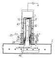
(実施の形態1)
図1乃至図3を用いて本発明の実施の形態1について説明する。図1は実施の形態1に係るプラズマ処理装置を示す断面図、図2は図1のZ−Z線における断面図、図3はプロセス圧力が異なる状況でのプラズマボリュームおよびプラズマチャンバの状態を示す説明図である。
【0024】
実施の形態1に係るプラズマ処理装置は、図1および図2に示すように、プラズマを生成するためのプラズマチャンバ1がプロセスチャンバ2の上部に配置され、プラズマチャンバ1の下部に細長いプラズマチャンバ開口部35を有している。
【0025】
プラズマチャンバ1の外部には、高周波を発生する高周波電源3と、電界を生成するレゾネータ4と、レゾネータ4からの電界を内部に導入するための誘電体窓6とが配置されている。誘電体窓6は左右両側に配置されている。さらに、レゾネータ4で生成された電界が外部へ漏れるのを防ぐために、シールド板5が配置される。
【0026】
プラズマチャンバ1内部の上面付近には、励起ガスを導入するためのライン状に並んだ導入孔を有する励起ガス導入ノズル15が配置され、下方には反応ガスを導入するためのライン状に並んだ導入孔を有する反応ガス導入ノズル16が配置される。
【0027】
尚、プラズマチャンバ1は、基板8の進行方向Aに対して斜めに配置されてもかまわない。また、励起ガス導入ノズル15および反応ガス導入ノズル16は、それぞれプラズマチャンバ1の中央以外にも配置され得る。
【0028】
プラズマチャンバ1は、下部プラズマチャンバ1Bと上部プラズマチャンバ1Tとに分割されている。プロセスチャンバ2と下部プラズマチャンバ1Bとは、下部チャンバベローズ24により柔軟に接続される。さらに、下部プラズマチャンバ1Bと上部プラズマチャンバ1Tとは、上部チャンバベローズ25により柔軟に接続される。下部チャンバベローズ24および上部チャンバベローズ25は、例えば楕円形のステンレス鋼板を溶接して形成される。
【0029】
プラズマチャンバ1の外部には、下部チャンバベローズ24と上部チャンバーベローズ25とに対応して、下部ジャッキ40と上部ジャッキ41とが配置され、それぞれ、プロセスチャンバ2と下部プラズマチャンバ1B、下部プラズマチャンバ1Bと上部プラズマチャンバ1Tとに固定される。
【0030】
例えば下部ジャッキ40は、図2に示すように、4個のジャッキ42とモーター45とをギア44とロッド43とによって接続することで構成され、モーター45が回転することによりジャッキ42を昇降する。また、上部ジャッキ41も同様に構成され、モーター45が回転することによりジャッキ42を昇降し、上部プラズマチャンバ1Tを昇降させる。尚、昇降機構は他の如何なる構成もとり得る。
【0031】
プロセスチャンバ2の上面壁には、プラズマチャンバ開口部35と近接し平行に配置された細長い真空排気口13が配置される。プロセスチャンバ2の内部には、基板8を搭載する基板ホルダ7が基板搬送手段10の上に配置され、基板搬送手段10の動作により矢印Aの方向に搬送される。さらに、基板搬送手段10より下側に、少なくともプラズマチャンバ開口部35から真空排気口13までの長さを有する基板加熱手段9が配置される。
【0032】
また、ゲートバルブ11がプロセスチャンバ2の側面壁に配置され、基板8がゲートバルブ11を通して外部チャンバ、例えばロードロックチャンバからプロセスチャンバ2に搬入される。基板8への処理が終了すれば、ゲートバルブ11を通してプロセスチャンバ2から外部チャンバへ基板8が搬出される。
【0033】
尚、基板ホルダ7は、例えば抵抗体を内蔵した基板加熱機構を有してもかまわない。また、基板搬送手段10は、ローラー、ラックアンドピニオン等の如何なる構成でもかまわない。
【0034】
次に、プラズマ処理の動作について説明する。励起ガス導入ノズル15より導入された励起ガスは、誘電体窓6を通してレゾネータ4により励起され、反応ガス導入ノズル16より導入された反応ガスと混合されて、プラズマチャンバ開口部35を通って真空排気口13に排出される。
【0035】
一方、基板ホルダ7に搭載された基板8が、基板加熱手段9により所定温度に加熱されながら基板搬送手段10により矢印Aの方向に搬送され、上記混合ガスが導入されている処理ゾーンを通過する。
【0036】
このとき、所定温度に加熱された基板8の表面付近において混合ガスが気相反応し、基板8の表面が順次処理される。気相反応は、用いられるガス種に応じて、基板8の表面に対して堆積、エッチングまたはアッシングの何れかを行う。
【0037】
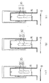
ここで、図3(a)〜(c)に、異なるプロセス圧力でのプラズマ領域30のボリュームおよびプラズマチャンバ1の状態を示す。
【0038】
図3(a)〜(c)は、プロセス圧力に応じてプラズマ領域30のボリューム、即ちプラズマ32およびアフターグロー33のボリュームが変化し、それに応じて下部プラズマチャンバ1Bおよび上部プラズマチャンバ1Tをそれぞれ昇降していることを示している。
【0039】
図3(c)は、図3(b)に比ベてプロセス圧力が低い状態を示す。図3(c)に示すように、プロセス圧力が低い場合、プラズマ領域30が大きくなるので、下部プラズマチャンバ1Bおよび上部プラズマチャンバ1Tをそれぞれ上昇させている。
【0040】
逆に、図3(a)は、図3(b)に比ベてプロセス圧力が高い状態を示す。図3(a)に示すように、プロセス圧力が高い場合、プラズマ領域30が小さくなるので、下部プラズマチャンバ1Bおよび上部プラズマチャンバ1Tをそれぞれ下降させている。
【0041】
このように、下部プラズマチャンバ1Bおよび上部プラズマチャンバ1Tが昇降することにより、ドリフト領域31を最適に設定し、即ちプラズマ領域30と基板8との距離を最適に設定することができる。また、上部プラズマチャンバ1Tを昇降することにより、有効な活性種のみが反応ガスと結合できるように、プラズマ領域30と反応ガス導入ノズル16との距離を最適に設定できる。
【0042】
(実施の形態2)
図4および図5を用いて本発明の実施の形態2について説明する。図4は実施の形態2に係るプラズマ処理装置を示す断面図、図5は図4のZ−Z線における断面図である。尚、実施の形態1と同様の構成については、説明を省略する。
【0043】
実施の形態2に係るプラズマ処理装置は、図4に示すように、励起ガスおよび反応ガスを導入するための配管が、それぞれプロセスチャンバ2の上面壁より接続され、プラズマチャンバ1の内部を側壁に沿って配置され、励起ガス導入ノズル15および反応ガス導入ノズル16に接続される。
【0044】
励起ガスを導入するための配管は、プロセスチャンバ2と下部プラズマチャンバ1Bと上部プラズマチャンバ1Tとに対応して分割され、それぞれ下部励起ガスベローズ28と上部励起ガスベローズ29とにより柔軟に接続される。また、反応ガスを導入するための配管は、プロセスチャンバ2と下部プラズマチャンバ1Bに対応して分割され、反応ガスベローズ27で柔軟に接続される。
【0045】
この構成により、プラズマチャンバ1の昇降にあわせて、励起ガス導入ノズル15および反応ガス導入ノズル16が移動し、その所定の位置を保つことができる。
【0046】
さらに、下部プラズマチャンバ1Bの内部には下部隔壁46が配置され、プロセスチャンバ2に固定されている。また、上部プラズマチャンバ1Tの内部には、下部隔壁46の内側に上部隔壁47が配置され、上部プラズマチャンバ1Tに固定されている。
【0047】
下部プラズマチャンバ1Bおよび上部プラズマチャンバ1Tの昇降にあわせ、上部隔壁47が移動することにより、伸縮機構、即ち下部チャンバベローズ24、上部チャンバベローズ25、下部励起ガスベローズ28、上部励起ガスベローズ29および反応ガスベローズ27を常に上部隔壁47でカバーし、チャンバベローズおよびガスベローズヘのプラズマ32による損傷および生成物の付着を防止するとともに、チャンバベローズおよびガスベローズが伸縮するときに発生するダストパーティクルの飛散を防止することができる。
【0048】
【発明の効果】
以上の説明のように、本発明のプラズマ処理装置によれば、上部プラズマチャンバを下部プラズマチャンバに対して昇降させ、励起ガス供給手段と反応ガス供給手段との距離を可変にすることにより、反応ガスのプラズマ化による被処理基板の損傷を防止して、安定したプラズマ処理を行うことができる。
【0049】
また、下部プラズマチャンバをプロセスチャンバに対して昇降させ、プラズマ領域と被処理基板表面との距離を可変とし、かつ励起ガス供給手段と反応ガス供給手段との距離を可変とすることにより、広範囲のプロセス条件下での高品質のプラズマ処理が可能となり、常に安定したプラズマ処理を行うことができる。
【0050】
また、被処理基板を基板加熱手段により加熱すると共に基板搬送手段により搬送しながら、連続して被処理基板にプラズマ処理を行うことができる。
【図面の簡単な説明】
【図1】 実施の形態1に係るプラズマ処理装置を示す断面図である。
【図2】 図1のZ−Z線における断面図である。
【図3】 プロセス圧力が異なる状況でのプラズマボリュームおよびプラズマチャンバの状態を示す説明図である。
【図4】 実施の形態2に係るプラズマ処理装置を示す断面図である。
【図5】 図4のZ−Z線における断面図である。
【図6】 従来のプラズマ処理装置を示す断面図である。
【図7】 (a)〜(c)は従来のプラズマ処理装置におけるプラズマボリュームの状態を示す説明図である。
【符号の説明】
1 プラズマチャンバ
1B 下部プラズマチャンバ
1T 上部プラズマチャンバ
2 プロセスチャンバ
3 高周波電源
4 レゾネータ
5 シールド板
6 誘電体窓
7 基板ホルダ
8 基板
9 基板加熱手段
10 基板搬送手段
11 ゲートバルブ
13 真空排気口
15 励起ガス導入ノズル
16 反応ガス導入ノズル
21 電界生成器
24 下部チャンバベローズ
25 上部チャンバベローズ
27 反応ガスベローズ
28 下部励起ガスベローズ
29 上部励起ガスベローズ
30 プラズマ領域
31 ドリフト領域
32 プラズマ
33 アフターグロー
34 放射性種ボリューム
35 プラズマチャンバ開口部
40 下部ジャッキ
41 上部ジャッキ
42 ジャッキ
43 ロッド
44 ギア
45 モーター
46 下部隔壁
47 上部隔壁[0001]
BACKGROUND OF THE INVENTION
The present invention relates to a semiconductor device such as an integrated circuit, a liquid crystal display device, or a device for manufacturing a solar cell, and more particularly to a plasma processing apparatus.
[0002]
[Prior art]
In recent years, a parallel plate plasma CVD apparatus in which electrodes are arranged in parallel has been used as a method for forming a thin film on a substrate. In the parallel plate plasma CVD apparatus, since the plasma is positioned 2 to 5 cm above the surface of the substrate, the gas is excited and decomposed by the plasma potential, and at the same time, the decomposed gas reacts with the surface of the substrate, May be damaged or contaminated.
[0003]
As a method for solving such a problem, as disclosed in Japanese Patent Laid-Open No. 8-279498, there has been proposed a plasma processing apparatus in which plasma is disposed remotely from a substrate. This plasma processing apparatus is shown in FIG.
[0004]
In the plasma processing apparatus shown in FIG. 6, the
[0005]
An
[0006]
An excitation
[0007]
The
[0008]
The
[0009]
In FIG. 6, 2 is a process chamber, 5 is a shield plate, 7 is a substrate holder, 9 is a substrate heating means, 10 is a substrate transfer means, 11 is a gate valve, and 13 is a vacuum exhaust port.
[0010]
[Problems to be solved by the invention]
However, in the plasma processing apparatus described above, the volume of the
[0011]
FIG. 7 (c) shows a state where the process pressure is lower than that in FIG. 7 (b). As shown in FIG. 7C, when the process pressure is low, the
[0012]
Conversely, FIG. 7A shows a state in which the process pressure is higher than that in FIG. 7B. As shown in FIG. 7A, when the process pressure is high, the
[0013]
Also, the volume of the
[0014]
Thus, the volume of the
[0015]
The present invention has been made in view of the conventional problems as described above, and even when process conditions such as process pressure or high-frequency output are different, by keeping the distance between the plasma region and the substrate constant, An object of the present invention is to provide a plasma processing apparatus capable of high-quality processing under a wider range of process conditions.
[0016]
[Means for Solving the Problems]
To achieve the above object, a plasma processing apparatus of the present invention comprises a plasma chamber to generate a plasma, which is connected to the plasma chamber, a substrate to be processed therein to be plasma processed by the plasma generated in the plasma chamber a plasma processing apparatus including a process chamber is disposed, wherein the plasma chamber is lower plasma chamber a reaction gas supplying means provided with the vertically movably connected through a lower extension mechanism to the process chamber And an upper plasma chamber connected to the lower plasma chamber through an upper telescopic mechanism so as to be movable up and down and provided with an excitation gas supply means .
[0017]
The process chamber includes a substrate transfer unit that transfers the substrate to be processed independently of the reaction gas supply unit, and a substrate heating unit that is disposed below the substrate transfer unit and heats the substrate to be processed. It is characterized in that it comprises a.
[0018]
Further, the upper telescopic mechanism and the lower telescopic mechanism are each constituted by a bellows .
[0019]
According to the plasma processing apparatus of the present invention, the upper plasma chamber is moved up and down with respect to the lower plasma chamber, and the distance between the excitation gas supply means and the reaction gas supply means is made variable so that the reaction gas supply means is brought into the plasma region. Without being covered, only active active species can be combined with the reaction gas, and the substrate to be processed can be prevented from being damaged by the reaction gas becoming plasma, and stable plasma treatment can be performed.
[0020]
Further, the lower plasma chamber is moved up and down with respect to the process chamber, the distance between the plasma region and the reactive gas supply means and the surface of the substrate to be processed is made variable , and the distance between the excitation gas supply means and the reactive gas supply means is made variable . As a result, the distance between the plasma region and the surface of the substrate to be processed can be optimally set according to the process conditions, and the drift region can be optimally set to prevent damage to the surface of the substrate to be processed. Therefore, high-quality plasma treatment can be performed under a wide range of process conditions. Further, the reactive gas supply means is not covered with the plasma region, and only effective active species can be combined with the reactive gas, so that stable plasma treatment can be performed at all times.
[0021]
Further, the substrate to be processed can be continuously subjected to plasma processing while being heated by the substrate heating unit and being transferred by the substrate transfer unit.
[0022]
DETAILED DESCRIPTION OF THE INVENTION
An embodiment of the present invention will be described with reference to FIGS.
[0023]
(Embodiment 1)
A first embodiment of the present invention will be described with reference to FIGS. 1 is a cross-sectional view showing the plasma processing apparatus according to the first embodiment, FIG. 2 is a cross-sectional view taken along line ZZ in FIG. 1, and FIG. 3 shows the state of the plasma volume and the plasma chamber under different process pressures. It is explanatory drawing.
[0024]
As shown in FIGS. 1 and 2, the plasma processing apparatus according to the first embodiment includes a
[0025]
Outside the
[0026]
An excitation
[0027]
The
[0028]
The
[0029]
Outside the
[0030]
For example, as shown in FIG. 2, the lower jack 40 is configured by connecting four
[0031]
On the upper surface wall of the
[0032]
The
[0033]
The substrate holder 7 may have a substrate heating mechanism with a built-in resistor, for example. Further, the substrate transport means 10 may have any configuration such as a roller, a rack and pinion.
[0034]
Next, the operation of the plasma processing will be described. The excitation gas introduced from the excitation
[0035]
On the other hand, the
[0036]
At this time, the mixed gas undergoes a gas phase reaction near the surface of the
[0037]
Here, FIGS. 3A to 3C show the volume of the
[0038]
3 (a) to 3 (c), the volume of the
[0039]
FIG. 3C shows a state where the process pressure is lower than that in FIG. As shown in FIG. 3C, when the process pressure is low, the
[0040]
Conversely, FIG. 3A shows a state in which the process pressure is higher than that in FIG. As shown in FIG. 3A, when the process pressure is high, the
[0041]
As described above, when the
[0042]
(Embodiment 2)
A second embodiment of the present invention will be described with reference to FIGS. 4 is a cross-sectional view showing the plasma processing apparatus according to the second embodiment, and FIG. 5 is a cross-sectional view taken along the line ZZ in FIG. Note that the description of the same configuration as that of the first embodiment is omitted.
[0043]
In the plasma processing apparatus according to the second embodiment, as shown in FIG. 4, pipes for introducing excitation gas and reaction gas are respectively connected from the upper surface wall of the
[0044]
The piping for introducing the excitation gas is divided corresponding to the
[0045]
With this configuration, the excitation
[0046]
Further, a
[0047]
As the
[0048]
【The invention's effect】
As explained above, according to the plasma processing apparatus of the present invention, by raising and lowering the upper plasma chamber with respect to the lower the plasma chamber, the distance between the reaction gas supplying means and the excitation gas supply means to the variable, the reaction It is possible to prevent damage to the substrate to be processed due to gas plasma, and perform stable plasma processing.
[0049]
Further, by lifting the lower plasma chamber to the process chamber, by the distance between the plasma region and the surface of the substrate to be processed is variable, and the distance between the excitation gas supply means and the reaction gas supply means is variable, a wide range of High-quality plasma treatment under process conditions becomes possible, and stable plasma treatment can always be performed.
[0050]
Further, the substrate to be processed can be continuously subjected to plasma processing while being heated by the substrate heating unit and being transferred by the substrate transfer unit.
[Brief description of the drawings]
FIG. 1 is a sectional view showing a plasma processing apparatus according to a first embodiment.
FIG. 2 is a cross-sectional view taken along the line ZZ in FIG.
FIG. 3 is an explanatory diagram showing a plasma volume and a state of a plasma chamber in a situation where process pressures are different.
FIG. 4 is a cross-sectional view showing a plasma processing apparatus according to a second embodiment.
5 is a cross-sectional view taken along line ZZ in FIG.
FIG. 6 is a cross-sectional view showing a conventional plasma processing apparatus.
FIGS. 7A to 7C are explanatory views showing a state of a plasma volume in a conventional plasma processing apparatus.
[Explanation of symbols]
DESCRIPTION OF
Claims (3)
前記プラズマチャンバに接続され、前記プラズマチャンバで生じたプラズマによってプラズマ処理される被処理基板が内部に配置されるプロセスチャンバと、を備えたプラズマ処理装置であって、
前記プラズマチャンバは、前記プロセスチャンバに下部伸縮機構を介して昇降可能に接続されると共に反応ガス供給手段が設けられた下部プラズマチャンバと、前記下部プラズマチャンバに上部伸縮機構を介して昇降可能に接続されると共に励起ガス供給手段が設けられた上部プラズマチャンバとにより構成されていることを特徴とするプラズマ処理装置。A plasma chamber for generating plasma;
Which is connected to the plasma chamber, the target substrate to be plasma processed by the plasma generated in the plasma chamber is a plasma processing apparatus and a process chamber which is disposed therein,
The plasma chamber is connected to the process chamber through a lower expansion / contraction mechanism so as to be movable up and down, and is connected to the lower plasma chamber through an upper expansion / contraction mechanism. And an upper plasma chamber provided with excitation gas supply means .
前記プロセスチャンバは、前記被処理基板を前記反応ガス供給手段とは独立して搬送する基板搬送手段と、前記基板搬送手段の下方に配置されて前記被処理基板を加熱する基板加熱手段とを備えていることを特徴とするプラズマ処理装置。The process chamber includes a substrate transfer unit that transfers the substrate to be processed independently of the reaction gas supply unit, and a substrate heating unit that is disposed below the substrate transfer unit and heats the substrate to be processed. A plasma processing apparatus.
前記上部伸縮機構及び前記下部伸縮機構は、それぞれベローズにより構成されていることを特徴とするプラズマ処理装置。The plasma processing apparatus, wherein each of the upper and lower extension mechanisms is constituted by a bellows.
Priority Applications (4)
| Application Number | Priority Date | Filing Date | Title |
|---|---|---|---|
| JP17490999A JP3662779B2 (en) | 1999-06-22 | 1999-06-22 | Plasma processing equipment |
| TW089111844A TW449826B (en) | 1999-06-22 | 2000-06-16 | Plasma processing apparatus |
| US09/598,574 US6490994B1 (en) | 1999-06-22 | 2000-06-21 | Plasma processing apparatus |
| KR10-2000-0034476A KR100387908B1 (en) | 1999-06-22 | 2000-06-22 | Plasma Processing Apparatus |
Applications Claiming Priority (1)
| Application Number | Priority Date | Filing Date | Title |
|---|---|---|---|
| JP17490999A JP3662779B2 (en) | 1999-06-22 | 1999-06-22 | Plasma processing equipment |
Publications (2)
| Publication Number | Publication Date |
|---|---|
| JP2001003175A JP2001003175A (en) | 2001-01-09 |
| JP3662779B2 true JP3662779B2 (en) | 2005-06-22 |
Family
ID=15986826
Family Applications (1)
| Application Number | Title | Priority Date | Filing Date |
|---|---|---|---|
| JP17490999A Expired - Fee Related JP3662779B2 (en) | 1999-06-22 | 1999-06-22 | Plasma processing equipment |
Country Status (4)
| Country | Link |
|---|---|
| US (1) | US6490994B1 (en) |
| JP (1) | JP3662779B2 (en) |
| KR (1) | KR100387908B1 (en) |
| TW (1) | TW449826B (en) |
Families Citing this family (19)
| Publication number | Priority date | Publication date | Assignee | Title |
|---|---|---|---|---|
| JP4627373B2 (en) * | 2001-02-06 | 2011-02-09 | 浜松ホトニクス株式会社 | Surface treatment equipment for printed circuit boards |
| US7056416B2 (en) * | 2002-02-15 | 2006-06-06 | Matsushita Electric Industrial Co., Ltd. | Atmospheric pressure plasma processing method and apparatus |
| JP4338355B2 (en) * | 2002-05-10 | 2009-10-07 | 東京エレクトロン株式会社 | Plasma processing equipment |
| DE10239083B4 (en) * | 2002-08-26 | 2009-09-03 | Schott Ag | Device for supplying a process chamber with fluid media and their use |
| KR100488348B1 (en) * | 2002-11-14 | 2005-05-10 | 최대규 | Plasma process chamber and system |
| NL1022155C2 (en) * | 2002-12-12 | 2004-06-22 | Otb Group Bv | Method and device for treating a surface of at least one substrate. |
| CN1968763A (en) * | 2004-06-16 | 2007-05-23 | Ppg工业俄亥俄公司 | Methods for removal of polymeric coating layers from coated substrates |
| US20060118240A1 (en) * | 2004-12-03 | 2006-06-08 | Applied Science And Technology, Inc. | Methods and apparatus for downstream dissociation of gases |
| US7912657B2 (en) * | 2006-12-06 | 2011-03-22 | Applied Materials Israel, Ltd. | Method and system for providing a compensated auger spectrum |
| KR100888659B1 (en) * | 2007-09-04 | 2009-03-13 | 주식회사 유진테크 | Substrate processing unit |
| US8039052B2 (en) * | 2007-09-06 | 2011-10-18 | Intermolecular, Inc. | Multi-region processing system and heads |
| JP5075793B2 (en) * | 2008-11-06 | 2012-11-21 | 東京エレクトロン株式会社 | Movable gas introduction structure and substrate processing apparatus |
| JP5398358B2 (en) * | 2009-05-29 | 2014-01-29 | 三菱重工業株式会社 | Substrate support structure and plasma processing apparatus |
| US8852685B2 (en) * | 2010-04-23 | 2014-10-07 | Lam Research Corporation | Coating method for gas delivery system |
| JP5567392B2 (en) * | 2010-05-25 | 2014-08-06 | 東京エレクトロン株式会社 | Plasma processing equipment |
| WO2014098905A1 (en) * | 2012-12-21 | 2014-06-26 | Clearedge Power Corporation | Deposition cloud tower with adjustable field |
| JP2015090916A (en) * | 2013-11-06 | 2015-05-11 | 東京エレクトロン株式会社 | Substrate processing apparatus and substrate processing method |
| JP6713039B2 (en) * | 2018-12-26 | 2020-06-24 | 株式会社Fuji | Plasma gas irradiation device |
| JP7030915B2 (en) * | 2020-08-28 | 2022-03-07 | 芝浦メカトロニクス株式会社 | Plasma processing method and plasma processing equipment |
Family Cites Families (7)
| Publication number | Priority date | Publication date | Assignee | Title |
|---|---|---|---|---|
| JPH0729879A (en) | 1993-06-24 | 1995-01-31 | Sony Corp | Preparation of semiconductor device |
| JPH08167591A (en) | 1994-12-13 | 1996-06-25 | Ckd Corp | Flow straightening plate of semiconductor manufacturing device and electrode and flow straightening plate of cvd device, ashing device, and dry etching device |
| US5908565A (en) | 1995-02-03 | 1999-06-01 | Sharp Kabushiki Kaisha | Line plasma vapor phase deposition apparatus and method |
| JPH08260154A (en) * | 1995-03-20 | 1996-10-08 | Toshiba Mach Co Ltd | Induction coupling plasma cvd apparatus |
| JPH0997786A (en) * | 1995-09-29 | 1997-04-08 | Kobe Steel Ltd | Plasma processing method and device |
| US6029602A (en) * | 1997-04-22 | 2000-02-29 | Applied Materials, Inc. | Apparatus and method for efficient and compact remote microwave plasma generation |
| JP3161392B2 (en) * | 1997-11-28 | 2001-04-25 | 日本電気株式会社 | Plasma CVD apparatus and its dry cleaning method |
-
1999
- 1999-06-22 JP JP17490999A patent/JP3662779B2/en not_active Expired - Fee Related
-
2000
- 2000-06-16 TW TW089111844A patent/TW449826B/en active
- 2000-06-21 US US09/598,574 patent/US6490994B1/en not_active Expired - Lifetime
- 2000-06-22 KR KR10-2000-0034476A patent/KR100387908B1/en not_active IP Right Cessation
Also Published As
| Publication number | Publication date |
|---|---|
| US6490994B1 (en) | 2002-12-10 |
| TW449826B (en) | 2001-08-11 |
| KR100387908B1 (en) | 2003-06-18 |
| KR20010029828A (en) | 2001-04-16 |
| JP2001003175A (en) | 2001-01-09 |
Similar Documents
| Publication | Publication Date | Title |
|---|---|---|
| JP3662779B2 (en) | Plasma processing equipment | |
| KR101545525B1 (en) | Apparatus and method for processing a substrate edge region | |
| US6387208B2 (en) | Inductive coupling plasma processing apparatus | |
| US8864936B2 (en) | Apparatus and method for processing substrate | |
| KR100348575B1 (en) | A cleaning processing method of a film forming apparatus | |
| JPH0950992A (en) | Film forming device | |
| JP2011049570A (en) | Substrate processing apparatus, and semiconductor device manufacturing method | |
| JP2004288704A (en) | Plasma treatment device | |
| EP2080817B1 (en) | Method and apparatus for chamber cleaning by in-situ plasma excitation | |
| KR930003876B1 (en) | Plasma ashing method | |
| WO2006011336A1 (en) | High-frequency plasma processing apparatus and high-frequency plasma processing method | |
| JPH07321097A (en) | Treating device and washing method for ring body or baffle board used in the treating device | |
| TW200929352A (en) | Vacuum processing apparatus | |
| JPS592374B2 (en) | Plasma vapor phase growth equipment | |
| JP2740789B2 (en) | Processing method | |
| JP3908990B2 (en) | Local dry etching method | |
| JPS60100687A (en) | Vacuum treatment device | |
| KR100776831B1 (en) | Vacuum processing apparatus and method of using the same | |
| US11817291B2 (en) | Faraday shield and apparatus for treating substrate | |
| KR102095982B1 (en) | Substrate treating apparatus and substrate treating method | |
| JPS6112035A (en) | Semiconductor manufacturing device | |
| JPH0426538B2 (en) | ||
| JP4090156B2 (en) | Vacuum processing equipment | |
| JPH11111681A (en) | Decompression process device | |
| KR102095983B1 (en) | Substrate treating apparatus and substrate treating method |
Legal Events
| Date | Code | Title | Description |
|---|---|---|---|
| A977 | Report on retrieval |
Free format text: JAPANESE INTERMEDIATE CODE: A971007 Effective date: 20041201 |
|
| A131 | Notification of reasons for refusal |
Free format text: JAPANESE INTERMEDIATE CODE: A131 Effective date: 20041221 |
|
| A521 | Request for written amendment filed |
Free format text: JAPANESE INTERMEDIATE CODE: A523 Effective date: 20050221 |
|
| RD03 | Notification of appointment of power of attorney |
Free format text: JAPANESE INTERMEDIATE CODE: A7423 Effective date: 20050221 |
|
| TRDD | Decision of grant or rejection written | ||
| A01 | Written decision to grant a patent or to grant a registration (utility model) |
Free format text: JAPANESE INTERMEDIATE CODE: A01 Effective date: 20050315 |
|
| A61 | First payment of annual fees (during grant procedure) |
Free format text: JAPANESE INTERMEDIATE CODE: A61 Effective date: 20050324 |
|
| R150 | Certificate of patent or registration of utility model |
Free format text: JAPANESE INTERMEDIATE CODE: R150 |
|
| FPAY | Renewal fee payment (event date is renewal date of database) |
Free format text: PAYMENT UNTIL: 20080401 Year of fee payment: 3 |
|
| FPAY | Renewal fee payment (event date is renewal date of database) |
Free format text: PAYMENT UNTIL: 20090401 Year of fee payment: 4 |
|
| FPAY | Renewal fee payment (event date is renewal date of database) |
Free format text: PAYMENT UNTIL: 20100401 Year of fee payment: 5 |
|
| FPAY | Renewal fee payment (event date is renewal date of database) |
Free format text: PAYMENT UNTIL: 20100401 Year of fee payment: 5 |
|
| FPAY | Renewal fee payment (event date is renewal date of database) |
Free format text: PAYMENT UNTIL: 20110401 Year of fee payment: 6 |
|
| LAPS | Cancellation because of no payment of annual fees |